Cost Modelling and Concurrent Engineering for Testable Design A thesis submitted to Brunel University for the degree of Doctor of Philosophy by Jochen Helmut Dick, Dipl. Ing.Univ. Department of Electrical Engineering and Electronics Brunel University April 1993 -., p - 4..:;: 1

Welcome message from author
This document is posted to help you gain knowledge. Please leave a comment to let me know what you think about it! Share it to your friends and learn new things together.
Transcript

Cost Modelling and Concurrent Engineering for Testable Design
A thesis submitted to Brunel University
for the degree of Doctor of Philosophy
by
Jochen Helmut Dick, Dipl. Ing. Univ.
Department of Electrical Engineering and Electronics
Brunel University
April 1993
-., p
- 4..:;: 1

To Stefani

Acknowledgements
I would like to acknowledge the guidance, encouragement and support of Professor A. P.
Ambler throughout this research. I am grateful to Dr. E. Trischler for his support of this
work and many helpful discussions. I am also grateful to my colleagues in the test
engineering team at Siemens-Nixdorf and the ESPRIT EVEREST project. In particular I
would like to thank Dr. C. Dislis whose technical support and critical appraisal has been
extremely valuable, and Dr. J. Armaos for the helpful discussions in the field of Monte
Carlo simulation.
i

ABSTRACT
As integrated circuits and printed circuit boards increase in complexity, testing becomes
a major cost factor of the design and production of the complex devices. Testability has
to be considered during the design of complex electronic systems, and automatic test
systems have to be used in order to facilitate the test. This fact is now widely accepted in
industry. Both design for testability and the usage of automatic test systems aim at
reducing the cost of production testing or, sometimes, making it possible at all. Many
design for testability methods and test systems are available which can be configured into
a production test strategy, in order to achieve high quality of the final product. The
designer has to select from the various options for creating a test strategy, by maximising
the quality and minimising the total cost for the electronic system.
This thesis presents a methodology for test strategy generation which is based on
consideration of the economics during the life cycle of the electronic system. This
methodology is a concurrent engineering approach which takes into account all effects of
a test strategy on the electronic system during its life cycle by evaluating its related cost.
This objective methodology is used in an original test strategy planning advisory system,
which allows for test strategy planning for VLSI circuits as well as for digital electronic
systems.
The cost models which are used for evaluating the economics of test strategies are
described in detail and the test strategy planning system is presented. A methodology for
making decisions which are based on estimated costing data is presented. Results of
using the cost models and the test strategy planning system for evaluating the economics
of test strategies for selected industrial designs are presented.
11

Table of Contents
1. Introduction ................................................................................................................. 1 1.1. Description of the Problem ................................................................................... 1 1.2. Testing, Error Free Design and Production ........................................................... 4 1.3. Structure of the Thesis .......................................................................................... 6
2. Test Methods ................................................................................................................ 8 2.1. Introduction .......................................................................................................... 8 2.2. Description and Classification of Test Methods ..................................................... 10
2.2.1. Design for Testability Methods for VLSI Devices .......................................... 10 2.2.1.1. Ad-Hoc Methods
................................................................................... 13 2.2.1.2. Scan Structure Methods ......................................................................... 14 2.2.1.3. Self Test Methods
.................................................................................. 16
2.2.1.4. Design Specific Methods ........................................................................ 17
2.2.2. Tes t Generation Methods and Fault Simulation Methods ............................... 20
2.2.2.1. Test Pattern Generation Methods ........................................................... 20
2.2.2.2. ................................................. Fault Simulation ....................................
22 2.2.2.3. Testability Analysis ................................................................................
22 2.2.3. Tes t Application Methods .............................................................................
22 2.2.3.1. Component Test ....................................................................................
23 2.2.3.2. Bare Board Test ....................................................................................
23 2.2.3.3. Board Test .............................................................................................
23 2.2.3.4. System Test ...........................................................................................
27 2.3. Economical Impact ...............................................................................................
27 2.4. Summary
.............................................................................................................. 29
3. Test Strategy Planning ................................................................................................ 31
3.1. Introduction ..........................................................................................................
31 3.2. Definition of Test Strategy Planning and Classification of Test Strategy Planning Systems
........................................................................................................... 31
4. Test Economics ............................................................................................................ 36
4.1. Introduction ..........................................................................................................
36 4.2. Economic Modelling Techniques ..........................................................................
37 4.3. Methods for the Estimation of Life Cycle Cost
...................................................... 39
4.4. The Impact of Test Strategies on the Economics of Electronic Systems ................
41 4.5. Structure of the Test Economics Model ................................................................
44 4.6. A Life Cycle Test Economics Model for VLSI Devices and VLSI Based Systems and Boards ............................................................................................
47 4.6.1. The Test Economics Model for ASIC components ........................................
47 4.6.1.1. The Production Costs
............................................................................ 48
4.6.1.2. The Design Costs ...................................................................................
50 4.6.1.3. The Test Costs
....................................................................................... 51
4.6.2. The Test Economics Model for Boards ..........................................................
52 4.6.3. The Test Economics Model for Systems
........................................................ 56
4.6.4. The Test Economics Model for the Field Costs ..............................................
57 4.6.5. Consideration of Interest Rates........... 59
...........................................................
111

4.7. Summary ..............................................................................................................
60
5. ECOTEST .................................................................................................................... 61 5.1. Introduction .......................................................................................................... 61 5.2. The Philosophy of ECOTEST
............................................................................... 62 5.3. ECOTEST in a Test Engineering Environment ..................... 5.4. The EVEREST Test Strategy Planner
................................................................... 68
5.4.1. The Data Interfaces ....................................................................................... 68
5.4.2. The Functions of ECOTEST .........................................................................
72 5.5. Cost Modelling Techniques
................................................................................... 75 5.6. The Test Strategy Planner ..................................................................................... 78 5.7. Conclusions
.......................................................................................................... 81
6. Sensitivity Analysis ...................................................................................................... 82 6.1. Introduction
.......................................................................................................... 82
6.2. Description of the Problem ................................................................................... 83
6.3. Monte Carlo Methods for Dynamic Sensitivity Analysis ........................................ 86
6.3.1. Computation of Random Values for a Given Distribution Function ................ 89
6.3.1.1. Marsaglia Table Method ........................................................................ 90
6.3.1.2. Box and Miller Method .......................................................................... 91
6.3.1.3. Central Limit Theorem Method .............................................................. 91
6.3.1.4. Test of the Accuracy of the Methods ...................................................... 92
6.3.2. Correlation of Input Parameters .....................................................................
93 6.4. General Sensitivity Analysis ..................................................................................
95 6.4.1. Estimation of Mean Value and Variance of Sensitivity ...................................
96 6.4.1.1. The Algorithm .......................................................................................
96 6.4.1.2. Estimation Error of the Monte Carlo Simulation
.................................... 99
6.4.1.3. Results ................................................................................................... 104
............................................... 6.4.2. Estimation of the Maximum Sensitivity........... III 6.4.2.1. The Algorithm .......................................................................................
112 6.4.2.2. Reduction of the Sample Size
................................................................. 115
6.4.2.3. Results ................................................................................................... 116
6.5. Iterative Sensitivity Analysis ................................................................................. 117
6.6. Total Variation Sensitivity Analysis ....................................................................... 118
6.6.1. The Algorithm ............................................................................................... 119
6.6.2. Determination of the Number of Simulations Needed ..................................... 120 6.7. Summary
.............................................................................................................. 122
7. ECOvbs: A Test Strategy PLanner for VLSI based Systems ..................................... 124 125 7.1. Philosophy of ECOvbs ..........................................................................................
7.2. System Overview .................................................................................................. 13
7.3. The Design Description ....................................................................................... 13 3
7.4. The Test Method Descriptions and Test Equipment Descriptions .......................... 136 7.4.1. Syntax of Test Method Descriptions ..............................................................
137 7.4.2. Syntax of the Test Equipment Description
..................................................... 138
7.5. The Cost Models and the Cost Evaluator ......... ...............................................
139 7.5.1. The Cost Modelling Technique
...................................................................... 140
7.5.2. Description of the Cost Models .....................................................................
144 7.6. Calculation of Fault Spectrum and Defect Spectrum .............................................
146 7.6.1. Calculation of Defect Spectrum after Manufacture .........................................
148
IV

7.6.2. Calculation of Fault Spectrum ....................................................................... 149
7.6.3. Calculation of Defect Spectrum for Repair .................................................... 150
7.7. The Test Strategy Planner ..................................................................................... 152 7.8. The User Interface ................................................................................................ 155
7.8.1. The User Commands of ECOvbs ................................................................... 156 7.8.1.1. The ECOvbs handler
.............................................................................. 156 7.8.1.2. The DSR handler
................................................................................... 157 7.8.1.3. The TSP handler
.................................................................................... 158 7.8.1.4. The CM handler
..................................................................................... 160 7.9. Summary .............................................................................................................. 162
8. Test Economics Evaluation ......................................................................................... 163 8.1. Introduction .......................................................................................................... 163 8.2. The Economics of Boundary Scan
................................... .......... 163 ........................... 8.3. Test Strategy Planning with ECOTEST ................................................................
169 8.3.1. Test Strategy Planning for Selected Industrial Designs
................................... 169
8.3.2. Test Strategy Planning with the Total Variation Method ................................
176 8.3.3. Test Strategy Planning for RAND_CIRC with the Total Variation Method
..................................................................................................................... 177
8.3.4. Test Strategy Planning for DEMO_CIRC with Inaccurate Input Data 179 8.3.5. Test Strategy Planning for Industrial Designs with the Total Variation Method ......................................................................................................
181 8.4. Test Strategy Planning with ECOvbs
.................................................................... 182
8.5. Summary ..............................................................................................................
188
9. Conclusions .................................................................................................................. 190 9.1. Summary of the Work ...........................................................................................
190 9.2. Conclusions
.......................................................................................................... 191
9.3. Future Research .................................................................................................... 192
References ........................................................................................................................ 195
V

List of Figures
Figure 1: The increasing IC circuit density [Sed92] ....................................................... 1 Figure 2: The increasing gate per pin ratio [Sed92] ....................................................... 2 Figure 3:
.............................. The quality options for test strategies ............................... 5 Figure 4: Classification of Scan Structures
.................................................................... 16 Figure 5: Structure of test strategies ..............................................................................
32 Figure 6: Classification of test economics model parameters .......................................... 43 Figure 7: Life cycle model for electronic systems with regard to test ............................. 46 Figure 8: Flow diagram of board level phases ................................................................
53 Figure 9: The test/repair loop of the test application phase ............................................
55 Figure 11: Field repair loop .............................................................................................
58 Figure 12: Shareability of test resources ............ ...... ........................................................
66 Figure 13: The ECOTEST architecture ...........................................................................
69 Figure 14: Example of a cost model and its internal representation ..................................
75 Figure 15: Structure of the cost model calculator ............................................................
80 Figure 16: Standard error of Monte Carlo simulation for group 1
.................................... 100
Figure 17: Standard error of Monte Carlo simulation for group 2 .................................... 100
Figure 18: Standard error of Monte Carlo simulation for group 3 ....................................
101 Figure 19: Mean sensitivity for a 1% variation and no DFT .............................................
102 Figure 20: Mean sensitivity for a 20% variation and no DFT ...........................................
102 Figure 21: Mean sensitivity for a I% variation and scan path ...........................................
103 Figure 22: Mean sensitivity for a 20% variation and scan path .........................................
103 Figure 23: Mean sensitivity for a I% variation and self test .............................................
104 Figure 24: Mean sensitivity for a 20% variation and self test ...........................................
104 Figure 25: 99% range of sensitivity with a I% variation, no DFT
.................................... 106
Figure 26: 99% range of sensitivity with a 10% variation, no DFT ..................................
107 Figure 27: 99% range of sensitivity with a 20% variation, no DFT
.................................. 107
Figure 28: 99% range of sensitivity with a 1% variation, scan path .................................. 108
Figure 29: 99% range of sensitivity with a 10% variation, scan path ................................ 108 Figure 30: 99% range of sensitivity with a 20% variation, scan path ................................
109 Figure 31: 99% range of sensitivity with a I% variation, self test .................................... 109 Figure 32: 99% range of sensitivity with a 10% variation, self test ...................................
110 Figure 33: 99% range of sensitivity with a 20% variation, self test ...................................
110 Figure 34: 99% range of sensitivity with a 1% variation, no DFT, low
production volume ......................................................................................... 111
Figure 35: 99% range of sensitivity with a 20% variation, no DFT, low
production volume ......................................................................................... III
Figure 36: Maximum sensitivity values ............................................................................ 117
Figure 37: Convergence of Monte Carlo simulation for no DFT ......................................
121
Figure 38: Convergence of Monte Carlo simulation for scan path .................................... 122
Figure 39: Convergence of Monte Carlo simulation for self test ...................................... 122
Figure 40: Architecture of ECOvbs .................................................................................
132
Figure 41: Sensitivity of the total cost in DM to the variation of parameter values in percent of the nominal value for In-circuit test .................................
167 Figure 42: ' Sensitivity of the total cost in DM to the variation of parameter
values in percent of the nominal value for boundary scan ................................ 167
VI

Figure 43: Sensitivity of the total cost difference in DM to the variation of parameter values in percent of the nominal value for In-circuit test minus boundary scan ......................................................................................
168 Figure 44: Cost of test strategies for automatic test strategy planning of
ERCO .................................................. ..........................................................
171 Figure 45: Cost of test strategies for automatic test strategy planning of PRI ..................
171 Figure 46: Cost of test strategies for automatic test strategy planning of
AM 2909 ........................................................................................................ 17 2
Figure 47: Cost of test strategies for automatic test strategy planning of AMS ................ 172 Figure 48: Cost of test strategies for automatic test strategy planning of SCR .................
173 Figure 49: Automatic test strategy planning by using the previous automatic
test strategy as the initial test strategy ............................................................ 174
Figure 50: Cost of automatically generated test strategies with different initial test strategies for the design PRI ....................................................................
175 Figure 51: Cost of automatically generated test strategies with different initial
test strategies for the design AMS .................................................................. 175
Figure 52: Distribution of total cost for final test strategy ................................................ 176
Figure 53: Distribution density function of total cost for RAND CIRC ...........................
178 Figure 54: Distribution function of total cost for RAND CIRC .......................................
178 Figure 55: Distribution function of total cost for DEMO CIRC
...................................... 180
Figure 56: Cost of board test strategies ........................................................................... 184
Figure 57: Number of faults after final test ...................................................................... 185
Figure 58: Number of remaining faults per test stage ....................................................... 186
Figure 59: Cost per detected fault in ECU per test stage for test strategy TS 1 ................. 187 Figure 60: Cost per detected fault in ECU per test stage for test strategy TS2 ................. 187 Figure 61: Cost per detected fault in ECU per test stage for test strategy TS3 ................. 188 Figure 62: Cost per detected fault in ECU per test stage for test strategy TS4 ................. 188
Vll

List of Tables
Table 1: Self test methods ............................................................................................ 17 Table 2: Cost impact of test application methods ......................................................... 29 Table 3: Cost estimation methods [Mad84]
.................................................................. 40
Table 4: Commands of ECOTEST ..............................................................................
74 Table 5: Ranges for Marsaglia Table ............................................................................
91 Table 6: Ranges for normal distribution test .................................................................
92 Table 7: Result of x2 test .............................................................................................
93 Table 8: Distribution characteristics of cost model parameters .....................................
97 Table 9: Parameter classification concerning its sensitivity ...........................................
105 Table 11: Main data of the industrial designs used for ECOTEST ..................................
169 Table 12: CPU times and cost savings by test strategy planning for industrial designs ......................................................................................................................
173 Table 13: Description of normal distributed parameters .................................................
177 Table 14: Description of normal distributed parameters .................................................
180 Table 15: Test Strategies for DEMO CIRC ..................................................................
180 Table 16: Run times for industrial designs
..................................................................... 182
Table 17: Main design data of computer board .............................................................. 182
Table 18: Test strategies for the computer board ........................................................... 183
viii

%. -iiapLý, l I
Chapter 1
Introduction
1.1. Description of the Problem
Introduction
The increase in the complexity of integrated circuits (figure 1) and the increase of the
gates per pin ratio (figure 2) of integrated circuits is now widely accepted to cause
tremendous problems for IC testing. Both values have been increasing exponentially with
time for the transistors per gate and with the generation of technology for the gates per
pin ratio for the last 20 years. With the increasing complexity of ICs, the production cost
per gate is decreasing, and if the testing cost would remain unchanged, they become
more important as they are becoming an increasing portion of the total cost [Tur90].
1000
100
0 y N C c0
10
1
1970 1975 1980 1985 1990
Year
Figure 1: The increasing IC circuit density [Sed92]

- 4J , Chapter 1 Introduction
1000
100
C
cC CP)
10
1 L-j
SSI MSI LSI VLSI ULSI
Level of Integration
Figure 2: The increasing gate per pin ratio [Sed921
But as the test of an IC is applied through the pins, the testing cost does not remain
unchanged, but increases for higher levels of integration. The expenses which are related
to test cost occur during the development for generating a test, which enables to detect
as many defects as possible, and during production for applying the generated test to the
ICs. The complexity of test generation increases linearly with the gate complexity of the
IC but exponentially with the accessibility of the gates. The accessibility of the gates is a
function of the gates per pin ratio. These dependencies lead to an exponential increase of
the test generation costs over time, if the methods for test generation remain unchanged.
A test is built upon test patterns which are applied to the IC through the pins. The cost
for test application is a function of the number of test patterns to be applied. The number
of test patterns again increases linearly with the number of gates and exponentially with
the gate per pin ratio. These reasons have caused the significant attention been paid to
the testing issue of the IC technology since the beginning of the 80's 1Wi1831.
The only way to keep testing cost in an acceptable bound is to develop new methods and
equipment. which facilitate test generation and test application. This includes the
development of new high-speed VLSI test equipment, tools for automatic test pattern
generation (ATPG) and design methodologies for facilitating the test generation and test
application tasks (design-for-testability, DFT).
1

Uhapter 1 Introduction
Most companies are aware of this testing problem and they have accepted some of the
DFT methodologies as well as ATPG systems or new test equipment. But all of these
methods have certain economic trade-offs. For example, a DFT method facilitates the
test and therefore reduces the related costs, but it may increase the production cost due
to an increase in the die size and a reduced production yield. ATPG systems have to be
purchased, and the price of such a system is still more than $50,000. And VLSI test
equipment has become extremely expensive with the increasing performance
requirements. The price for high-end testers are $5,000,000 or more.
The many options for performing the test of an IC allow to create many different test
scenarios, which assure a high quality of the IC. The test scenarios are called testing
strategies. An example for a test strategy is to design an IC such that an automatic test
pattern generation system can be used and a VLSI test equipment is applied to perform
the production test. A test strategy can be selected from those which fulfil technical
requirements. The selection criteria can range from a subjective assessment of the test
strategies by the persons who are involved in the implementation of it, to an economic
evaluation of the test strategy. The author proposes to use economic evaluations for test
strategy planning, because this method converts all impacts of a test strategy to a
common reference point, which is the cost in £, $, ECU, DM, or any other currency.
This is the only selection method which is fully objective. Other methods, such as the
assessment by experienced test engineers or design engineers, or the evaluation of some
costing parameters, which are based on different measure units, include a certain degree
of subjectivity from the person who is evaluating the test strategy. Therefore the selected
test strategy would be highly dependent on the person doing the evaluation.
This selection procedure becomes even more complicated when integrating the IC test
strategy into a test strategy for the entire system. An electronic system is typically built
upon printed circuit boards (PCB). In the past the testing problem of a PCB was not as
critical as for ICs. because accessibility to internal nodes was possible by using a special
class of test equipment, in-circuit tester. But today's surface mount technology for PCBs

Chapter 1 Introduction
uses wire separation of less than 100µm, double side mounted boards, and more than
2,000 internal nodes per board to access. The access to the internal nodes becomes
extremely difficult in many cases or even no longer possible. This fact was the main
motivation for developing the design methodology "boundary scan", which is
standardised under IEEE, known as the 1149.1 standard. This methodology allows to
access the pins of an IC through a serial shift register, which enables to get access to the
internal board nodes.
Boundary scan is an integrated design methodology, which can be used not only for
board testing, but also for troubleshooting at system level and in the field. This shows the
complexity of evaluating a test strategy which includes boundary scan. This test strategy
affects the IC design and production, the board production and test, the system test and
the field test. The evaluation of the economics of such a test strategy includes almost all
cost areas of the system during its life cycle.
For this reason the economics modelling techniques, which have been developed by the
author, consider the whole life cycle of the electronic system. This is the only way to
take into account all impacts of a test strategy for an objective evaluation.
1.2. Testing, Error Free Design and Production
One test strategy option is a strategy of not testing at all. This test strategy could be
economical if it was possible to develop and produce the products perfectly. This
involves a perfect design, perfect materials, a perfect manufacturing process and no
ageing of the product [Sed921. The term perfect is used here in the sense of "free of
errors or defects". But, since perfect products are unlikely in the near future, especially
under the aspect of ever increasing complexity, the major remaining option is testing a
product more or less in all phases of its He cycle. The "more-or-less" forms the test
strategy. which is defined by the criteria in figure 3.

Chapter 1 Introduction
Figure 3: The quality options for test strategies
The material quality affects the production yield of the device and therefore the required
test quality to achieve a certain quality level.
In the same A ay the manufacturing quality impacts the yield and therefore the test
quality requirements.
The test quality defines what percentage of all possible defects can be detected by a test
application. This test quality depends on the test generation capabilities, the test
equipment capabilities and the effort which is spent in test generation and test
application.
Under testing aspects the design quality, is the degree of "design-for-testability" which is
implemented in the design. This mainly affects the test capabilities and the economics of
achieving a certain level of test quality.
The linkage of these factors into a test strategy shows that test strategy planning is a
5

Chapter 1 Introduction
typical concurrent engineering task. A test strategy influences nearly all engineering
aspects of the product, and therefore they should be taken into account.
1.3. Structure of the Thesis
This thesis describes economics driven methods for test strategy planning, which take all
these factors into account. The test strategy planning system, which has been developed
by the author, comprises two test strategy planners. ECOTEST is a test strategy planner,
which is used for ASICs, and ECOvbs is a test strategy planner for VLSI based systems.
These tools can be used in combination in order to derive the most economic test
strategy for VLSI based systems. The tools take into account the concurrent engineering
aspects, which have just been described. This is a novel approach for test strategy
planning, which integrates the aspects of design, test and manufacture during the life
cycle of a system.
The rest of the thesis is organised as follows: Chapter 2 will present an overview on test
methods. The elements of test methods will be described. The test methods will be
classified and the important classes of test methods will be described.
Chapter 3 describes the process of test strategy planning and outlines a range of systems
which are used for test strategy planning. The scope of test strategies and test strategy
planning will be discussed.
Chapter 4 discusses the economics modelling aspect of test economics. It describes
various cost modelling techniques, and it will present the life cycle test economics model
which has been developed by the author.
Chapter 5 describes ECOTEST, the test strategy planner for ASICs. The philosophy of
ECOTEST is discussed. The usage of ECOTEST in test engineering is described and
discussed, the EVEREST test strategy planner [Dis92], which is the basis of ECOTEST
is outlined and the enhancements of ECOTEST against the EVEREST test strategy
planner will be described and discussed.
6

Chapter 1 Introduction
Chapter 6 describes a range of methods to study the impact of the inaccuracy of
economic parameters on the resulting cost. The parameters are generally studied in terms
of their impact on the sensitivity of the total cost. The description of the problem is
presented, the need and the gain of this work are discussed, and the different applications
of the sensitivity analysis are introduced. The author describes a method of analysing the
variation of all parameters at the same time and presents three applications of sensitivity
analysis.
In chapter 7, the author first discusses the philosophy of ECOvbs, the test strategy
planner for VLSI based systems, and the arising needs of such a system in industry. An
overview of the architecture of ECOvbs will be given and its components will be
described in detail.
Chapter 8 will present and discuss the results from analyses perfromed using the test
economics models which are described in chapter 4, using ECOTEST and using
ECOvbs.
The life cycle cost models described in chapter 4 were used to study boundary scan test
strategies. ECOTEST was used for two types of experiments. In the first set of
experiments, the author used the system for several large industrial designs in order to
prove its applicability. The second experiment is related to performing test strategy
planning with inaccurate data by using; the sensitivity analysis techniques which are
described in chapter 6. The last section of this chapter will present test strategy planning
results for a large computer board by using ECOvbs.
In chapter 9 the author draws the conclusions on his thesis. This includes a summary of
the work and several proposals for future work in this field. This is mainly related to
further improvements of ECOTEST, such as test partitioning and an improved
accessibility analysis. the full integration of field test aspects into ECOvbs and some ideas
on the automatic generation of life cycle test strategies.
7

t, napter z
Chapter 2
Test Methods
2.1. Introduction
Test Methods
The test of VLSI based systems aims to ensure a given quality for the system under test.
This quality level is typically defined in the early product planning phase, and it is driven
by cost analysis, market requirements, laws or by marketing or company strategies. A
test can be performed in several phases and levels of the design and manufacturing
process of the system. To achieve the required quality level, there are many different
options:
0 The quality level of the material used:
The complexity of material can range from raw material like solder to complex
devices like VLSI components.
0 The manufacture quality:
The manufacture quality impacts the defect rates of all parts created in the
manufacture process plus new defects introduced into the material during the
manufacture process. An example for these new defects may be a destruction of a
chip by too high temperatures during the soldering process.
" The test Quality:
The quality of a test is defined by the relation of the number of possible faults of
the device under test. The test quality depends mainly on the test method and the
characteristics of the device under test.
" The test level:
A test can be performed at many levels of manufacture. The author defines three
test levels as follows:
" The component test is applied to the components which are assembled into a
system. These are ICs, bare boards, or discrete elements. A component test
max he applied after the production of the components at the suppliers
8

%-. "ap`c1 -- Test Methods
facilities (production test) or at the customers facilities after the delivery of the
components (income test).
" The board test is applied to sub assemblies like printed circuit boards (PCBs)
or multi chip modules (MCMs).
" The system test is applied to the whole system in order to guarantee the
function of the whole system.
Component and board tests are options, which are used in addition to the system
test in order to make testing more economical.
" The test phase:
Quality assurance is usually defined in all phases of a product's life cycle. This
option is needed to detect occurring faults as early as possible, which is in many
cases an economical solution for the quality problem. Quality assurance may be
document review, computer simulation of the design model, a prototype
verification or the test of a manufactured device.
" The test strategy:
A test strategy is defined as the sequence of test activities at several life cycle
phases and levels of manufacture as described above. This definition of the term
test strategy is given in [Ben891.
This chapter will describe the state-of-the-art test methods for VLSI circuits and
complex boards and systems. A test method consists of three components:
The test generation is the process of generating stimuli for a circuit which will
demonstrate its correct operation [Wi183]. Various methods exist for test
generation. Which one is used depends on various aspects. such as the design
style or the availability of tools.
The test application is actual execution of the test for a given device. Test application
can be performed manually or automatically by using certain tools or equipment
for stimulating the device under test and measuring the results. The equipment
9

Chapter 2 Test Methods
can be incorporated into the circuit, which means that the circuit is self testing. The Design for Testability (DFT) methods are design styles and techniques, which are
more or less integrated into the functional design, and which facilitate the test
generation and test application, and therefore reduce the accompanied costs.
A test method always consists of these three components. Even if no design methods are implemented for facilitating the test, this is considered as a the DFT method no DFT. A
test method can be applied to parts of the design at several levels of assembly. The
definition, of which part of the design which test method is applied at which level, is
called the test strategy.
The following sections will present various DFT methods, test generation methods and
test application methods. The methods will be presented by categorising them, by
describing briefly the technique, and by describing its economical impacts.
2.2. Description and Classification of Test Methods
2.2.1. Design for Testability Methods for VLSI Devices
The facilities of VLSI led to heterogeneous and multi functional chips with increasing
complex functions [Zhu861. Attributes of these circuits are high gates-per-pin rates and
highly embedded functional blocks. By being embedded the blocks' accessibility is poor.
Due to the complexity of the functional blocks the controllability and observability of
internal nodes becomes more difficult. For testing, access to the inner circuit is essential.
So the cost for testing is increasing rapidly as the accessibility is decreasing. This fact is
confirmed by the conventional design process, which separates the design- and test-
phases. The need for considering test aspects during the design phase in order to
decrease test cost becomes evident.
So techniques, called Design for Testability (DFT), were developed to assure the
testability of VLSI circuits. The main purposes of DFT are
" The generation of high-quality tests is enabled.

Test Methods
Circuits are designed in such a way that an ATPG system can generate high-
quality tests sets automatically. Rules to be followed are checked by a DET-rule
checker accompanying the design phase.
0 The test itself becomes cheaper.
DFT techniques reduce the test set length by reducing the number of steps for
controlling and observing inner nodes. Also the usage of cheaper test equipment
is enabled by providing the circuit with self-test techniques.
Some of the techniques were developed for specific functions [Zhu88], some of them can
be applied [Wi183] generally. All techniques affect the design- and test-process in
different ways.
DFT methods in general can be defined as methods which aim in assuring high-quality
products by facilitating the test. The DFT methods studied here are specific for VLSI
products. This overview is divided into two parts :
" The general methods can be applied to every type of circuit. Mainly design
methods are described, which assure economic testing of VLSI products.
0 For some specific circuit structures, especially regular structures, there are
design-specific methods existing. Normally these structures are functionally
described. and so the classic methods for test pattern generation cannot be used,
because they are based on the logic structure. But because of the regularity of
these structures, formal methods to calculate high-quality test pattern sets were
derived.
DFT has different aspects: It can be seen as a philosophy as well for designers as for the
management. DFT must be considered in all design phases (functional design, logic
design. layout) by following specific rules to make a product testable. The DFT methods
can be partitioned into two groups :

Chapter 2 Test Methods
Ad-Hoc techniques can be applied quickly and easily. They are well suited for
application after the logic design. Because they are based on heuristics, no reliable
prediction of testability improvement is possible. These methods are mostly used to make
an existing design more testable.
Structured methods must be considered for the whole design. Therefore, they must be
applied from the beginning of the design. These methods are supported by CAD tools.
They usually decrease design times, and good testability of the circuit can be assured.
The expression "Design-For-Testability" fits much better for the structured methods,
because "Design-For-Testability" means designing for testability rather than redesigning
for testability.
Major testability aims of the methods are:
" Partitioning:
The effort for testing increases exponentially with the number of gates. Therefore
the effort can be reduced by dividing a circuit into smaller sub circuits for testing
purposes. Most of the Ad-Hoc techniques are based on this principle.
0 Increase of Controllability and Observability:
Especially for deeply sequential circuits controllability and observability of inner
nodes is very difficult. High controllability of control lines is important for the
testability of the controlled logic.
" Universal Testing:
Designs based on regular structures (e. g. PLAs) enable in some cases function-
independent testing. These methods are described in 3.2 and 5.2.
0 Dual Mode Design:
The circuit is provided by a mode pin to switch between test-mode and system-
mode.
1?

Chapter 2 Test 'Methods
" Scan Design Methods:
These methods enable access to inner nodes by using storage elements. The aims
are an increase of the testability and a decrease of the sequential depth for testing. By using a full scan design, sequential circuits can be modelled as combinational
circuits (sequential depth equals zero). Then automatic test pattern generation becomes much cheaper.
0 Self Test:
Self testing circuits are very efficient in terms of reduced test application cost.
Also the costs for test pattern generation can be very low by testing with random
patterns or testing exhaustively ([McC86]).
0 Compaction:
The responses at the outputs of the circuit under test are compacted internally.
Only a signature is evaluated.
2.2.1.1. Ad-Hoc Methods
This section will give an overview on the state-of-the-art Ad-Hoc techniques. Most of
them increase the testability for general logic designs.
1) Maximisation of Controllability and Observability
In general an increase of the controllability and observability of inner nodes of the circuit
under test leads to an increase of testability of the whole circuit. Especially the
controllability of control nodes, like clocks, set/reset lines, data select, enable/hold of
microprocessors, enable and read/write of memories, and control and address lines of bus
structures, sensitises the testability of the whole circuit. Also test points should be
included to the following nodes to increase the observability
buried control lines, outputs of memory elements, outputs of data-funnelling elements,
1I

%-flapicr Test Methods
redundant nodes, nodes with high fanout, global feedback paths.
2) Synchronisation of toralte Elements
For high-frequency circuits, problems like races can occur, especially for faulty circuits. To avoid these problems, memory elements should be clocked. For testing, all memory
elements should be clocked by the same source, and the clock line should be directly
controllable.
3) Initialisation
To reduce the test length, it should be easy to bring the memory elements into a defined
state. Therefore all memory elements should be provided with set- and reset-inputs and
these inputs should be easy to control.
4) Partitioning
As already mentioned, the effort of testing and test generation is exponentially related to
circuit complexity. So partitioning of circuits into smaller sub circuits for testing can
increase the testability.
2.2.1.2. Scan Structure Methods
Scan structure methods are considered during the whole logic design phase. The main
purpose of scan structures is to make memory elements directly accessible or to control
and observe inner nodes by direct access. Typically, scan structures operate in two
modes. In system mode, the circuit operates to fulfil its normal function. In test mode,
the scan elements can be observed and controlled directly. The type of access depends on
the scan structure type.
The scan structures can be classified by four properties ([Tri821) :
" Degree of Integration
If a scan element is integrated into the normal function, it is an internal scan
14

%-tic&PL%, L :- Test Methods
structure. If extra scan elements are used to access internal nodes, we have an
external scan structure. Internal scan structures are mostly used to reduce the
sequential depth of the circuitry, where external scan structures are used for
partitioning and accessibility purposes.
0 Completeness of Scan Structures :
If all memory elements of a circuit are scan elements, and these elements are
integrated into a scan-path-chain, we call this structure full scan path. A
combinational model of the circuit can then be derived, to generate test patterns
by an ATPG system for combinational logic. To reduce the silicon overhead, the
partial scan path is used, where only a subset of memory elements are accessible
via a scan path. These elements are selected in order to reduce the sequential
depth and to make nodes with low accessibility more accessible.
0 Type of access :
The scan elements can be accessed serially or in parallel. For serial access, the
elements are interconnected into one shift register. For parallel access, the scan
elements are grouped. For every group, direct access is then possible. The groups
can be selected via a decoder.
0 Scannability of Scan Structures :
The author distinguishes between passive scan structures, which allow only
observation (scanning) of the scan elements, and active scan structures, which
allow both, observation and control. Passive scan structures are typically external,
and they are used for diagnostic purposes. While running in system mode, the
circuit can be monitored.
By this classification, we can derive the following classification tree:
Iý

. -A-L4kJ«,, L Test Methods
Figure 4: Classification of Scan Structures
2.2.1.3. Self Test Methods
The main purpose of self test methods is the reduction of test application cost and test
generation cost by the following reasons
" Test equipment costs increase dramatically due to the high pin count and
performance requirements of VLSI circuits. Also the lifetime of high-end testers
becomes shorter, because requirements like maximum pin number or maximum
operating frequency are increasing very fast. Self test methods enable the usage
of cheap testers, because the function of the tester is only to control the test.
0 The complexity of VLSI based systems (VBSs) makes in-field tests costly. Self
test methods support the diagnosis. and so the in-field testing of components in
assembled systems becomes cheaper.
0 Self test enable exhaustive testing and random testing ([McC86]). This reduces
the test generation cost. because the test sets must not be generated
16

l, [1iiptcr L Test Methods
deterministically. For random testing, the fault coverage can be predicted by
using testability measures (see 3.1.2). Costly fault simulation can be omitted. For
exhaustive testing, the fault coverage is always 100%.
" Self test structures can be applied at system speed. Therefore a self test is rather
dynamic than static. That means, that dynamic failures are covered by self tests.
A test method must consist of a strategy for generating input stimuli to be applied,
evaluating the responses of the device under test and an implementation mechanism
([McC86]). Every self-test-method must fulfil these requirements. Some methods
accomplish all requirements, some of them support self testing only partly. A complete
self test must consist of all three elements. The most important self test methods are
listed in table 1.
Structures for Stimuli linear feed back shift register (LFSR), non-linear shift register Generation NFSR
, ROM, counters
Structures for Output parallel signature analysis, serial signature analysis Response Analysis Structures for Self Test built in logic block observer (BILBO), in system at speed test Architectures (ISAST), circular self test path (CSTP)
Table 1: Self test methods
2.2.1.4. Design Specific Methods
General testability enhancing methods are not always the best option for a specific
functional block. Building blocks such as RAMs have a regular structure with specific
failure mechanisms. Using the scan approach for example, may incur a large area
overhead. On the other hand, there are many algorithms which test for specific fault
models, and the test strategy for the RAM can be based on these, thus taking advantage
of the regular structure. These observations apply mostly to embedded RAMs, where
accessibility often is a problem.
-another example of a regular structure is the PLA. In order to obtain a high fault
coverage, cross point faults need to be considered in addition to stuck-at faults. Test
17 Li

`'"at" ` Test Methods
generation algorithms need to take these specific fault models into account. Many
general purpose test algorithms, as well as random test patterns, do not efficiently test
PLAs due to the high fan-out, fan-in and redundancy. Often deterministic and random
techniques are combined to arrive at a high fault cover test set within a reasonable time
and cost [Eic80]. There are also test generation algorithms for PLAs that arrive at a
function independent test set. These universal tests eliminate the test pattern generation
costs. However, modifications to the design are needed in order to apply the patterns and
observe the responses.
The test methods can be categorised according to the way they achieve their objective.
For example, in the PLA case, there are methods that use random patterns, self test
methods, parity checking methods and partitioning methods. These classifications are
intended only to make the study of test methods easier, and in fact, certain methods may
belong to more than one category. The classification of test methods is a continuous
process. However, methods which are obviously not suitable for an application or which
are only minor variations on an existing method should be considered carefully before
inclusion; the number of possible combinations increases very fast as the number of
available test methods increases, and run time should be taken into account. Hereinafter,
a selection of the most commonly used DFT methods for PLAs and RAMs are described.
The selection demonstrates the classification process and is not intended as a complete
set.
The Saluja method [Sa185] uses a shift register for partitioning. The shift re`ister is used
to control the product terms. However, in this case product terms are partitioned into
groups so that they can he tested in parallel. Therefore, the length of the shift register for
selecting product lines is shortened from the number of product lines to the number of
groups. The number of test patterns is also reduced.
The Fujiwara method (Fuj8l I uses a parity strategy. Adding a product line with its
associated connections will ensure an odd (or even) number of connections on every bit
lý

` IIQPL" Z- Test Methods
line. A cross point fault in the AND array will change the parity of a bit line. Faults in the
OR array can similarly be detected by adding an extra output line and a parity checker. In
order to achieve this, control of the product lines is needed, which is achieved by the use
of a shift register. An input decoder is also used, to ensure control of the bit lines. The
test used is a universal test set (low or nil test generation costs), which is function
independent, but requires vectors to be either pre stored or externally generated.
The Treuer method [Tre851 is also a parity checking method, but it eliminates the
requirement for a stored set of vectors. It has a very high fault coverage, covering all
single and most multiple cross point faults. The test vectors are self generated, and parity
signals are accumulated in a parity counter, the value of which is checked at specific
times.
The Daehn method [Dae8 l] is another self test method, which is based on partitioning.
BILBOs are used to partition the circuit, and are placed after input decoders, the AND
array and the OR array.
RAM test methods exploit the regular structure of the block in order to test for the
groups of faults specific to memories, due to their regularity and high density. One way
to test an embedded RAM is to implement test structures which ease the application of a
specific memory test algorithm. One example of this type of method is the
implementation of the March test, a simple, widely used memory test algorithm [Dea89].
The modified hardware required would be shift registers for data in and a comparator
register, as well as a modification to the address register to also act as an up/down
counter. The March test can then be applied and the responses evaluated using an N bit
comparator. For a memory with an N bit word, the test length would be 2m+8Nm. m
being the number of words. This algorithm tests to 100% for single stuck at faults (ssa).
but does not perform ver`, well for pattern sensitive faults. The addition of simple control
and test generation circuitry would make the memory self testable. It is relatively simple
to modify the shift register/counter/comparator arrangement to implement more complex
19

. A1apLcr - Test Methods
algorithms. The test generation effort is almost nil.
Another group of methods uses pseudo random patterns for self test of RAMs. The
Inman [I1186] method converts the data input and address registers into maximum length
LFSRs and randomly sets the write enable. The application of patterns is repeated until
the required fault cover (determined probabilistically) is achieved. The requirements for
the method are: the data input register as well as the address register can also act as a
shift register and a maximum length LFSR with preset. A data output register is required
that can act as a MISR with preset. A hard wired word size comparator is necessary, as
well as a2 to 1 MUX to select between functional and test mode. LFSRs are needed to
produce the random write enable signals, as well as the set of initial seeds. A set of
counters is also needed in order to scan in the new seed, keep a count of the number of
tests applied and ensure that all cell addresses have been accessed. Also a small amount
of random logic is required to handle the clock control of the registers and control each
test stage. The number of test patterns depends on the number of repetitions of the test.
2.2.2. Test Generation Methods and Fault Simulation Methods
To apply a test, test input stimuli and output responses must be derived as a
precondition. These test patterns must be evaluated in respect to their fault coverage.
Test patterns are generated for the detection of failures. These failures are represented by
a fault model. Algorithms were derived to generate a test pattern set automatically
(Automatic Test Pattern Generation, ATPG) and to evaluate the test pattern set by
simulating the faulty circuit. ATPG is typically supported by a testability analysis. Beside
guiding the decision-making-process of the ATPG testability analysis is also used for
improving the testability of circuits by applying Ad-Hoc DFT strategies. In the following
the author gives a brief overview on the algorithms.
2.2.2.1. Test Pattern Generation Methods
The purpose of ATPG algorithms is to determine a test vector, which detects a given
20

Chapter 2 Test Methods
fault ([DiG89]), or to prove the given fault as a redundant fault. For most algorithms, a
test vector for a given fault must satisfy two objectives ([DiG89]) :
0 The first objective is to activate the fault.
" The second objective is to observe the effect of the fault at one of the circuit
outputs.
The algorithms can be divided into four categories ([DiG89]):
0
40
0
Tabular Methods:
For each possible input combination output values for the fault-free and each
faulty circuit are calculated. This approach is used in [Hwa86] and [Gho89]. In
[Dic87] it is shown, that cases can be constructed, where the algorithm fails due
to complexity problems.
Algebraic Methods:
The mostly used algorithm of this class is based upon the Boolean difference
method ((Se1681, [Lar89]).
Functional Methods:
Tests are derived from the functional description of the circuit ([Hey89], [Su841).
Within a class of realisations, the test generation is possible for stuck-at-faults
([Poa631).
Gate Level Algorithms:
Algorithms based on the gate level description of the circuit generate test vectors
typically for every single stuck-at fault. The basic algorithm is the D-algorithm
([Rot661). Based on the D-algorithm, the algorithms PODEM ([Goe81 ]), FAN
([Fuj83]) and SOCRATES ([Sch88]) were developed to improve the efficiency
for very complex circuits. All these algorithms were developed for combinational
circuits. For sequential circuits, the algorithms were extended to solve the
problem. that the circuit responses depend on the circuit state in addition to the
input stimuli ((\1ar86)). This matter of fact leads to a new complexity dimension
for generating test patterns, because the number of states can increase
?1

Chapter 2 Test Methods
exponentially with the number of memory elements.
2.2.2.2. Fault Simulation
Fault simulation tools are used together with ATPG to speed up the TPG process and to
reduce the test set length (without fault simulation a test pattern must be generated for
every testable fault). Existing test sets (e. g. the functional test patterns used for logic
simulation) can be evaluated by using a fault simulator. Several approaches ([Arm72],
[Sch84], [Rog85]) were presented for general circuits, and for scan-based circuits
Parallel-Pattern-Single-Fault-Propagation ([Wai85]), Critical-Path-Tracing ([Abr84]) or
Fast-Fault-Simulation ([Ant87]) led to high efficiency in terms of computing time.
2.2.2.3. Testability Analysis
Testability analysis is a method of grading the testability of a circuit by measuring the
controllability and observability of the internal nodes. As mentioned earlier, especially for
sequential VLSIs the results of ATPG and fault simulation are very poor. The need of
DFT in order to improve the testability is evident. One approach is to apply structured
DFT methods like the internal scan path. For Ad-Hoc DFT strategies information is
needed on the location of testability problems. Therefore testability analysis tools were
introduced, which are based on testability measures ([Go1801, [Gra79], [Kov8l],
[Ben80], [Rat82]. [Tri84], [Brg84]). Due to neglecting signal correlations caused by
reconvergent fanouts, the results of the testability analysis do not always give the exact
information about circuit regions with poor testability ([Agr82]).
Testability measures are also used to improve the search heuristics within the ATPG.
2.2.3. Test Application Methods
In this section the author will give an overview on the most important test application
methods and their. use. The description will include the test application procedure, the
required DEl methods, the test equipment and the fault coverage which can be achieved.
)1

Chapter 2 Test Methods
The test application methods are grouped into component tests, board tests and system
tests.
2.2.3.1. Component Test
A component can be tested by an income test in the same way as it should be tested by
the component supplier by the production test. This might be a complex VLSI test for
VLSI components or a test of the specification for simple passive components like
resistors or capacitors. In the production phase the test is usually applied to each
component, whereas an income test strategy mostly applies the test only to a sample per
delivered lot. The sample size depends on the delivery quality and the deviation from this
quality and may range from 0 (no incoming test is performed) to all incoming
components.
2.2.3.2. Bare Board Test
The bare board test tests the wiring of an unassembled PCB. It uses special bare board
test equipment, which includes capabilities to contact the board, to generate a test
program automatically by analysing a golden device, and to perform the test. The fault
coverage is 100% of the opens and shorts of the wiring on the bare board.
2.2.3.3. Board Test
In contrast to the component test, the task of board test is not only a go/no go test but
also a fault diagnosis in terms of fault location for repair. This means, that the quality of
a test is described by the fault coverage and the fault diagnosis capability.
By a visual inspection, a board is inspected visually by a person for gross defects such
as solder splashes. The degree of inspection depends on the type of test following the
visual inspection. This test method is very cheap but has a low fault coverage
The manufacture defect analyser (MDA) is an In-circuit tester that examines the board
construction. Nomially power is not applied to the board to be tested. As a DFT
23

Chapter 2 Test Methods
requirement, test pads are needed for all nodes to be adapted. The test equipment is a
special MDA equipment, which requires a separate fixture for each device under test. Only passive elements and the board construction can be tested. This includes the test of
resistors, capacitors and the solder defects such as shorts or some opens. The fault
diagnosis is straightforward, i. e. the fault can be located in parallel with the identification
of the fault. Multiple fault identification can be performed in one test run.
An In-circuit test (ICT) examines construction of a board by isolating and examining
each component on the board as an independent entity. Therefore the board must be
accessed at each electrical node on board level through a fixture called "bed-of-nails".
Each component on the board is tested in power-on condition by both stimulating the
inputs and evaluating the outputs of the component through the bed-of-nails fixture. This
requires back driving the outputs of the components, which are connected with the
inputs of the component to be tested. The following DFT methods are required:
" Test pads must be designed for all nodes to be adapted.
" It must be assured, that back driving does not destroy the components.
9 Every component must be separately testable.
The test equipment is a special ICT equipment. A special purpose fixture for every board
type to be tested is needed. If the DFT requirements are fulfilled, the board level fault
coverage of static faults can be 100%. Dynamic faults cannot be covered, if the ICT is
performed statically. A dynamic In-circuit test requires more DFT and a more expensive
In-circuit tester. This type of test is able to cover some of the dynamic faults. The
coverage of analog defects depends on the capabilities of the ICT equipment. The fault
diagnosis is straightforward. Multiple fault identification can be performed in one test
run.
A functional test accesses the board under test (BUT) only by the edge connectors. A
functional tester emulates the environment of the board, i. e. the system in which the
board will be used. Typical (functional) test stimuli are applied, and the board's output
responses are evaluated. If the BUT fails the test, guided probe or fault. dictionary
24

Chapter 2 Test Methods
techniques are used to locate the fault. The generation of test data is done by using a
simulation system. The design must be logically partitioned, so that the test units for
which test data should be applied, can be easily accessed from the edge connector. In
addition, all chip level DFT requirements, such as the ability of initialisation, must be
fulfilled. Testability is an essential requirement for functional board testing. The
functional board test uses a special board tester, which consists of configurable digital
and analog signal sources and measuring devices. For the application of guided probe
techniques, probe sensors are needed. The achievable fault coverage strongly depends on
the DFT methods applied. Dynamic faults can only be covered, if the test system is
capable for performance tests at the required speed. Analog parts can only be tested, if a
clear separation from the digital parts is possible. Multiple fault detection and isolation in
one run is not normally possible.
A combinational test combines in-circuit test and functional test. The functional test
capabilities are combined with the in-circuit test capabilities and its diagnostic
capabilities. Depending on what type of test to run, the DFT requirements are a
combination of the ICT and functional test requirements. A special combinational test
equipment is needed. The fault coverage capabilities are a combination of the ICT and
functional test fault coverage. The diagnosis capability is equivalent to the ICT
capability.
An emulation test is a special variation of the functional test, where specific board
components are replaced by an adaptation to the test equipment. The function of the
replaced component is emulated by the test system. Typical components which are
emulated are:
" Processors: The processor is replaced by a processor oriented device (POD),
which is capable of imitating the processor's function and timing.
0 Memories: The memory on board is replaced by the tester's memory. This allows
to control the processor's action directly by the test system.
0 Busses: The processor on board is controlled via the main bus of the board. This
ýý

Chapter 2 Test Methods
means, that no board component needs to be replaced by an emulation adapter. An emulation test is used for real time tests of complex processor boards. The DFI'
requirements are the same as for the functional test. A functional tester with additional
processor specific emulation units can be used as test system. The emulation test is
applied mainly for the dynamic test of the processor and its periphery. Therefore the fault
coverage for dynamic faults and the diagnostic capabilities for dynamic faults are high.
For covering static functional faults and construction faults, an additional static test
should be applied.
The memory test is a special feature of testing, which enables to apply algorithmic test
patterns rather than deterministic test patterns. The number of test patterns for memory
test are typically very high, but the test patterns are of algorithmic nature and can
therefore easily generated online. This type of generation reduces the test pattern
memory requirements of the test system. The memories on board must be directly
accessible. Any functional test system with online test data generation feature may be
used. The fault coverage is 100% for memories or other devices, which can be tested by
algorithmic test data.
A burn-in test aims to force early life failures by accelerating the time of operation. This
is achieved by overdriving parameters, which cause the early life failures, such as
temperature or voltage. No special DFT is required. A burn-in test is executed in
combination with any of the test equipment mentioned here. If environmental parameters
such as the temperature should be overdriven, an equipment to overdrive these
parameters. e. g. a climate chamber. is needed. The type of faults covered depends on the
test equipment used. The percentage of early life failures forced depends on the early life
behaviour of the device under test and the acceleration factor of the burn-in test.
A hot bed tester is a one-of-a-kind tester used to verify that the board under test
actually operates in the final product [Pyn86]. Normally a hot bed tester exists of the
entire product except the board to test. The board to test is inserted into the hot bed
tester, which can also be called the reference system. The test consists of evaluating the
correct operation of the whole product. No DFT is required. The fault coverage depends
26

Lnapter 2 Test Methods
on the percentage of functions being tested by the product's test operation. This type of
test covers best dynamic faults. The diagnosis is normally performed manually by skilled
technicians, who have detailed knowledge about the operation of the board.
2.2.3.4. System Test
The installation test is a procedure where the completely assembled product (the
system) is operated under field conditions. No special test equipment is required. The
only requirement is the ability to provide field conditions. All type of faults can be
covered. But normally the installation test aims in detecting dynamic functional faults and
faults caused by the final assembly. The faults coverage of manufacture faults is normally
not known, because a fault simulation of the test program would be too expensive. The
diagnosis of faults is usually done manually by the support of special diagnosis software.
A benchtop tester is a small test system which provides analog, digital functional and in
circuit test capabilities. The test system is not optimised for throughput, so the setup
times and test times are long compared to fully automatic test systems, such as an In-
circuit tester or a functional tester. The benchtop tester consists of a small computer, e. g.
a PC, a general purpose card cage and a variety of stimulus and measurement boards,
where the user can select from, in order to mix and match the test system to meet the
special test requirements. The fault coverage depends on the quality of the test mix.
Nearly any type of faults can be detected and located by this test system, if enough time
is given.
2.3. Economical Impact
It is becoming widely accepted that provision for test in the design stage is not only
desirable, but in many cases essential. This section will attempt to address the economic
aspects of DFT. These are taken into account in the economics model developed.
The advantages of incorporating ' DFT into a design are well known. One of the major
ones is the fact that test generation is made easier and test application times become
17

Chapter 2 Test Methods
shorter. Test generation for a large design can be a long and expensive process,
especially when a very high level of fault cover is required. Using appropriate design for
test techniques can alleviate this problem. Not only is test generation faster (and
therefore cheaper), but often a higher level of fault cover can be achieved. In the case of
self test techniques like signature analysis, the cost is reduced to simply predicting the
correct signature.
The use of self test techniques also reduces the test application costs by removing the
need for complex (and expensive) automatic test equipment (ATE). However, savings in
test application costs can be made in more indirect ways. For example, the ability to use
an inexpensive ATE for a project may free a heavily used ATE for use by other projects.
The net effect is a speeding up of the test process, and possibly earlier shipping of the
product. In a competitive market, this is a distinct advantage.
One reason that DFT methods may not be chosen is the possible increase in design time
due to the introduction of new techniques. To solve this problem, the test support system
being developed will provide the designer with data on the chosen test methods, so that
implementation can be made easier. In any case, it should be born in mind that the design
time increase can be minimised if the CAD system supports automatic overlay of test
structures. One more point is that making the investment in terms of design time may
well lead to considerable savings in terms of overall development time, as expensive
redesign due to inadequate testability provision can be eliminated. In some cases, it has
been found that the structured design style required to implement some test methods led
to an overall reduction in design time.
The provision for testability also leads to the manufacture of high quality products. It is
cheaper to discover faults in the early stages of a product's life cycle. The increased
reliability of high quality products has definite advantages for the manufacturer's
reputation.
Conversely. DFT structures often involve extra silicon. This has been a major reason why
28

` Ililpmr /- Test Methods
DFT methods were often discounted as uneconomical. However, the only way to decide
on the suitability of a DFT technique is to make a careful economic evaluation of all the
relevant factors. The economics model has been developed for that purpose. Taking the
concept one step further, the economic model can be used as a method of choosing
which mix of DFT techniques to use in a particular situation.
The economical impact on the board and the system of various test application methods,
which are presented here, is shown in table 2. It presents a qualitative cost impact on the
various design and production phases of the system and on the board yield. The cost
impact is rated as follows:
" ++ means high additional costs
0+ means moderate additional costs
"o means no cost impact
"- means small cost savings
0 -- means high cost savings
Test Application Method
Design Test Preparation
Board Manufacture
Board Yield
Board Test
System Test
Income test 0 + 0 +/++ +/- - Bare board test o + o +/++ +/- - Visual Inspection o 0 0/+ + - - MDA +/o + o o +/- o ICT + + +/o 0 + -- Functional test + ++ o o +/++ -- Combi test + +/++ +/o 0 + -- Emulation test + + o/+ 0 + -- Memo test o + 0 0 - - Burn-in test o 0 0 + - - Hot bed test o o/+ o 0 - - Installation test o + 0 0 0 - Benchtop test o + 0 0 0 +
Table 2: Cost impact of test application methods
2.4. Summary
In this chapter. the author described selected test methods, which are widely used in
industry. This included the description and classification of Design-for-Testability
methods, test generation methods and test application methods. The economical impact
29

Chapter 2 Test Methods
of the test methods was discussed, and a qualitative cost evaluation of the test
application methods was performed. The actual cost of a test method depends on many
factors, and these can only be derived for an actual design.
The test strategy planning uses the knowledge which was presented in this chapter in
order to create an appropriate test strategy for a given design. The approaches for test
strategy planning will be presented in the next chapter. If the economics of test methods
are to be taken into account, a quantitative evaluation method for test methods is
needed. The related techniques will be described in chapter 4.
30

Chapter 3
Chapter 3
Test Strategy Planning
3.1. Introduction
Test Strategy Planning
This chapter describes the process of test strategy planning and outlines a range of
systems which are used for test strategy planning. The author will define and discuss the
scope of test strategies and test strategy planning. Test strategy planning is driven by
selection criteria, which are different for the test strategy planning systems. The author
will discuss these criteria and will show, that the economics of a test strategy is the most
relevant optimisation criterion. A classification of existing test strategy planning systems
will show that there is no general test strategy planning system, which considers all
aspects of a test strategy. The test strategy planner ECOvbs (see chapter 7) which was
developed by the author is the first system, which takes this general view of a test
strategy into account.
3.2. Definition of Test Strategy Planning and Classification of Test Strategy
Planning Systems
Test strategy planning for electronic systems is defined as the task, in which the
specification of a test strategy for an electronic product is performed. This task is based
upon more or less knowledge about the design, the test methods which form the test
strategy, and the environment, in which the product is developed and designed. What test
strategy planning actually includes, depends on what a test strategy embodies. Therefore
test strategy planning ranges from the optimisation of a Design-for-Testability method,
such as partial scan selection ([Tri83], [Che89], [Gun90]) or BIST selection ([Bar92])
to a global approach as performed in this thesis.
A test strategy planning system is a system which supports the specification or the
implementation or both of a test strategy. Due to different meanings of a test strategy,
the scope of test strategy planning systems can be completely different. Some test
31
L

1 Test Strategy Planning
strategy planning systems target at optimising a single DFT method for a given design,
some aim at specifying a DFT strategy for a heterogeneous ICs, some aim at selecting a
test equipment from different suppliers and some aim at defining a procedure of test
applications during the manufacturing process. The author has therefore structured test
strategy planning by classifying the target test strategy into several classes (Fig. 5).
Figure 5: Structure of test strategies
The DFT strategies classification was taken from [Dis92]. There, test strategies are
related to structured design to test methods for an integrated circuit. For an integrated
circuit the planning of a test strategy is concentrated on planning the design-for-
testability strategy. Different DFT methods can be applied in heterogeneous designs and
the test application is mostly a single test equipment, which is used once or at most twice
(wafer test and component test) in the production phase. Also, by planning a DFT
strategy, the selection of a test equipment is mostly included, because the selected DFT
methods determine the type of test equipment to be used. This can range from an
expensive VLSI test equipment, with DFT depending facilities such as algorithmic
3:

Chapter 3 Test Strategy Planning
pattern generators or special serial registers for loading and unloading the scan path, to a
cheap PC with some extensions, which is used to control the test of a fully self testable
IC.
An earlier use of the term test strategy and test strategy planning was related to the test
application scenario in the production ([Dav82], [Pyn86], [Mah88], [Ham87]). Even the
selection of a new test equipment from the market can be seen as test strategy planning ([Dav82], [Ben87], [Pab87]). Most of these test strategy planning systems consider the
economics as a selection factor, but the economic evaluation is limited purely to test
application.
The global test strategy approach which is incorporated in this work by the test strategy
planner ECOvbs, takes all factors of test methods into account for defining a test
strategy. The author's definition of a test strategy is as follows:
A test strategy is an arrangement of test procedures in the production of a
system and the specification of appropriate design methods and test
generation methods which support the test of the system.
This means that a test strategy defines a scenario of test methods used for testing
different parts of the system at different levels of assembly. A test method consists of
three components, namely design-for-testability, test generation and test application, as
defined in the previous chapter. This view of test strategies is especially important since
the introduction of boundary scan, which was the first design-for-testability method
specially designed for board level test. Today many DFT methods, including BIST. are
proposed for facilitating the board level test. Therefore an important economic factor of
a test strategy for an electronic system is the DFT methods used. On the other hand,
evaluating DFT strategies without evaluating the related test application scenario can
also lead to misleading results, especially if the DFT methods can be used for several
tests at different levels of assembly, such as boundary scan, or even scan path.
Iý

%, A, apLcr .3 Test Strategy Planning
The factors which affect the selection of a test strategy are technical constraints, which
can immediately reduce the number of possible solutions, and costing parameters, which
are used to quantify the advantages and disadvantages of the test strategies against each
other, and which are subject to optimisation. Some systems only use technical constraints
for test strategy planning [Laf91 ]. If several solutions towards a test strategy are
possible, the user of the system is free to select one. If costing parameters are used for
test strategy planning, these can range from a single parameter to complex test
economics models.
An example for test strategy planning by optimising a single parameter is a partial scan
selection, which aims at finding a minimum number of flip flops, which breaks all loops in
a design ([Che89], [Gun90]). Some systems use several costing parameters, but these are
based on different measure units ([Aba85], [Jon86], [Aba89]). The problem here is to
compare the different costing parameters to each other. Therefore user defined weighting
factors have been introduced, which allow the user to define the importance of each
parameter for the selection procedure. But this makes test strategy decision strongly
dependent on the user's opinion and no more objective. What the user thinks to be
important may not necessarily relate to what is actually important.
What is important for selecting a test strategy out of technically possible solutions, is to
minimise the total cost. which is affected by the test strategy. This idea lead to the
approach, which was first developed at Brunel University ([Dis89], [Dis91 ]), and which
are used in this thesis. This method is called economics driven test strategy planning.
Previous economics driven test strategy planning systems concentrated on optimising
DFT strategies. The system ECOvbs (see chapter 7). which was developed by the
author, aims at optimising the complete test scenario for an electronic system. from
design-for-testability selection for the IC components to the final test. This system will be
described in chapter 7.
The economical evaluation of a test strategy automatically allows to compare different
,ý

t, uapLci Test Strategy Planning
costing factors, such as chip area and test time, to each other, because all parameters are
converted into real costs. The common measure unit is then £, $, DM or any other
currency. This conversion of all cost affecting parameters into the total costs is
performed by a cost model. The weighting factors are part of the cost model, which
means that the weighting of costing parameters is no longer left to the user. The
weighting factors in the cost model convert the costing parameters into real cost, which
is an objective conversion into a common measurement unit.
The next chapter will describe the techniques to develop these cost models, and it will
present the various cost models which were developed by the author, and which are used
in the test strategy planning systems ECOTEST and ECOvbs.
35

Chapter 4
Chapter 4
Test Economics
4.1. Introduction
Test Economics
This chapter will describe the terms and techniques of economics modelling in general
and test economics modelling in particular. These techniques are used to develop a
hierarchical life cycle test economics model which is used in the test strategy planning
systems ECOTEST and ECOvbs developed by the author. The test economics model
will be described.
The terms "economics model" and "cost model" have the same meaning throughout this
thesis. The term cost is more general. It is not only used for financial parameters but also
for technical parameters, such as test time or chip area. Therefore the term cost model is
often used for models which calculate these non financial parameters. In the author's
approach, cost is always related to financial parameters. This is one reason why the term
"economics model" is used instead of cost model. Another reason is the educational
aspect. People mostly relate the term cost to additional cost but not to cost savings. But
the scope of an using economics models is to save cost. The term economics is much
more related to cost savings or to the positive effect of a method or strategy. Therefore
the term economics model is better suitable for the usage in test strategy planning than
the term cost modelling, because it automatically includes the saving aspect.
Section 4.2 will describe economics modelling techniques by describing some terms, the
various types of economics models, and the techniques of developing economics models.
In section 4.3 the economic impact of test methods. especially the impact of DFT. will
be described and discussed. Section 4.4 will present the structure of the test economics
model. In section 4.5 the life cycle test economics model, which has been developed by
the author, will be described.
36

Chapter 4 Test Economics
4.2. Economic Modelling Techniques
The main objective of economics modelling is to provide a method for analysing the
financial costs of a product or procedure or both before they actually occur. Economics
modelling is a predictive technique for performing an economic analysis. An economics
model allows to estimate the economics of a certain product by predicting the values of
the cost-affecting the parameters. A test economics model is an economics model, which
is used to predict the economics of test strategies. The analysis is performed to make
certain decisions. These decision range from the purchase of equipment to methodical
strategies, like design strategies. Therefore an economics model can be seen as a decision
model [Din69].
A decision model is built upon parameters and variables, which are used to determine a
target value [Din69]. In a decision model the target value is subject to optimisation by
determining the optimal combination of the variables for a given set of parameters. The
parameters are assumed to be fixed for a certain decision to be made, whereas the
variables can vary within a defined range. Various techniques exist for determining the
optimum mix of variables. These techniques are known as linear or non linear
programming techniques [Lue731. Using test economics modelling techniques for test
strategy planning means that all costing parameters, which vary from test strategy to test
strategy are the variables of the decision model, and all costing parameters, which are
test independent are the parameters of the decision model. The linear programming
techniques assume that a variable is continuous in its defined range. This is not the case
for the test strategy planning task, because the variable values are fixed for a given test
strategy, and each test strategy is defined by its own set of values for the variables. So
the optimisation problem for test strategy planning is a combinational optimisation
problem, and therefore it is different from the classical linear and nonlinear programming
problem. For that reason these techniques cannot be used for the test strategy planning
task. Nevertheless the test economics model can be seen as a decision model, but with a
different meaning of the term "variable". In order to avoid. misunderstandings, the author
17

Chapter 4 Test Economics
calls the "variable" a test dependent parameter.
In order to consider all effects of a decision, an economics model should consider all
costs during the He cycle of the product, which is subject to the decision. Such a life
cycle cost model considers all the costs from the design to the wear out of the product.
The process of economics modelling and its applications, such as test strategy planning,
is composed of four objectives [Wue84], and therefore it should be performed in four
steps:
0 The interpretation objective aims at recognising the costing relations and the
structure of the cost. The cost structure is used to categorise the costing
parameters in all phases of the life cycle. This structure can also be hierarchical,
as this is the case in the test economics model.
0 The estimation objective is aims in the development of costing relations, which
describe the relation of the cost effecting parameters. These relations can be
modelled for example in mathematical equations.
" The modelling objective is related to modelling the cost for a given product by
using the previous two objectives. This includes the gathering of input data for
the economics model as well as the calculation of the cost.
0 The configuration objective is the analysis of the calculated cost and the decision
making process, which is based on this economic analysis. A life cycle cost
analysis is defined in [Bla78] as follows:
A life cycle cost analysis may he defined as the systematic analytical process of
evaluating various alternative courses of action with the objective of choosing
the best way to employ scare resources.
This definition matches exactly the scope of test strategy planning. Therefore the
configuration objective is the actual test strategy planning process.
The result of the interpretation objective and the estimation objective is the actual
economics model. In the author's approach, this economics model is developed once and
is used multiply as part of the test strategy planning system. The modelling objective and
38

Chapter 4 Test Economics
the configuration objective are applied each time a test strategy planning session is
performed. The test strategy planning systems ECOTEST and ECOvbs provide features,
which support the process of achieving the last two objectives. The first two objectives
are reached by the development of the economics model, which has been done by the
author and which will be described in the following sections. The last two objectives can
be reached by using the test strategy planning systems ECOTEST and ECOvbs for a
given electronic system, which provide features for gathering the data and calculating the
cost (the modelling objective) as well as features for evaluating and assessing the various
alternative test strategies.
4.3. Methods for the Estimation of Life Cycle Cost
The determination of the life cycle cost has to be performed very early in the design
phase. This is because the decision on the test strategy includes design decisions which
have to be taken before the electronic system is fully implemented. This leads to the
major problem of economics based test strategy planning. The life cycle costs are not
known in this phase of the life. They must be predicted, and in fact this prediction is
subject to uncertainty. This problem cannot be solved completely, but by using various
methods the risk. which is related to this uncertainty, can be minimised. One of these
methods was developed by the author and is described in chapter 6. Another method is
the incorporation of the cost driving persons into the process of the modelling objective.
This fact is discussed in several publications (e. g. [Hil85], [Kir79]).
Several methods are proposed in the literature in order to estimate costs ([Mad841, see
figure 3). The author will present the most common methods and discuss them. Table 3
outlines and classifies these methods.
39

,.... ýr ..,. Test Economics
Methods Application Areas of Limitations require ents application
1. Judgement - experts/experience - early stage - subjective - expert judgement - rough product - situations without - undefined accuracy - educated guess definition risks - not applicable for - rough order of - analogy material - independent price negotiations magnitude crosschecks
- budget estimations 2. Parametric - historical data - concept - extrapolation of - cost estimation - regression analysis comparisons data bases and relationship(CER) - CER material - budget planning models is often
- statistics - tender analysis difficult - models - independent - estimation accuracy - cost formulas crosschecks can be vague 3. Detailed - time schedule - situations with - expensive and - work package estimation - statement of work high time consuming - work preparation and specification risk - low flexibility estimation - detailed technical - price negotiations - can lead to cost
- cost formulas material increases
- engineering cost - price tenders estimates
Table 3: Cost estimation methods [Mad84]
The judgmental methods are typically used in the very early phase of a product, where
no detailed information about the product is available. The methods are based upon
expert judgements, analogies, and estimations of a rough of order of magnitude. The
estimations can be driven by subjective criteria, and its application is very limited.
Due to that fact many authors propose to use the parametric methods. These methods
can lead to detailed results even in the early phase of a product's life. But its application
requires a certain level of knowledge about the design, production and field phases and
methods. A parametric cost model is a cost model which consists of primary and
secondary parameters. The primary parameters are the cost driving factors, and the
secondary parameters are costs or cost factors, which are derived from the primary
parameters or other secondary parameters by a mathematical equation. The most
important parametric method is the cost estimation relationship (CER) method. It uses
the experience from similar previous projects or products to develop a relation between
cost driving factors and the costs. This allows the usage of statistical methods like a
regression analysis.
The detailed methods are mostly based upon work packages. The project to estimate is
40

t.: napter 4 Test Economics
broken down into small work packages, for which an accurate estimation is possible. The
detailed cost estimates assume much more information about the project than the
parametric method, which may not be available when the estimation is performed.
The author has selected a combination of the detailed method and the parametric method
for the development of the test economics model. The test economics model is
structured into several smaller sub models, which are related to work packages. This
structure will be presented later in this chapter. The estimation of the costs of the work
packages is performed either by parametric models or a mixture of a parametric method
and a detailed method. For example, the design time of the ASICs is calculated by a
parametric method. The calculation of the assembly cost of a board is based on the
number of components per assembly type and the assembly cost per type. The calculation
of the assembly cost is a detailed method, but the calculation of the assembly cost per
assembly type is based on previous productions and is therefore parametric.
This mixture of the two estimation methods is a good trade-off between the accuracy of
the prediction and the cost for the prediction process. The test economics model is
intended to be used as the last step of the design specification. The structure of the test
economics model reflects the detailing level of a specification. Most of the information
about the parameters, which must be defined in order to determine the equations, is
available at the end of the specification.
4.4. The Impact of Test Strategies on the Economics of Electronic Systems
VLSI test strategies affect not only the economics of the VLSI itself but also the
economics of higher levels of assembly. and later stages of the product's life cycle. This
impact is described in a test economics model by the test dependent parameters. For
example, a self test which is designed for testing the component can also be used for the
field test and diagnosis. If for such a self test only the cost at component level are
evaluated, the result might be, that the self test is less economical than other test
strategies. But considering cost savings, which are made by using the self test in the field
41

Chapter 4 Test Economics
might invert this result. Thus an economic evaluation of test strategies should be done
for all test-sensitive cost areas of the product's life cycle.
In the same way the economic evaluation of test strategies for the entire system or for a
board, such as boundary scan, should take into account all costs, which can be affected
by the test strategy. The scope of this section is to identify the effect of test strategies on
the life cycle of electronic systems, and to develop a method, which enables to link the
test dependent parameters to the economics model.
Most test methods influence almost all phases of the life cycle. As an example, the test
method boundary scan is taken to illustrate this fact. Boundary scan has an influence on
the design cost of the components, the boards and the entire system. It does affect the
production cost of the component, the board and the system. It impacts the test and
diagnosis of the board and the system. And boundary scan can be used for field
diagnosis, and it therefore has an impact on the down times of a system in the field and
the field diagnosis cost. In addition, boundary scan can increase the product's quality,
which means, that the mean time between failure decreases, and again the down times are
decreased. Also time-to-market may be shortened by implementing boundary scan. This
is because of a lower risk of a redesign due to untestability of the design, and because of
lower fault diagnosis times for the system, which can easily exceed one week for a
complex VLSI based system. So the test method boundary scan does affect nearly all
phases of a product's life cycle. Therefore all these phases must be considered for
evaluating the economics of boundary scan.
By making a life cycle cost analysis a test strategy is not limited to the combination of
test methods for a part of the design, or a particular life cycle phase of the system. A
global test strate ! _v can be optimised for the whole system in all phases of the life cycle.
This leads to much better results from an economic point of view than optimising a test
strategy just for a part of the design of the life cycle. But the main objective of a test
strategy is to get the system work rather than to achieve a specific fault coverage for a
42
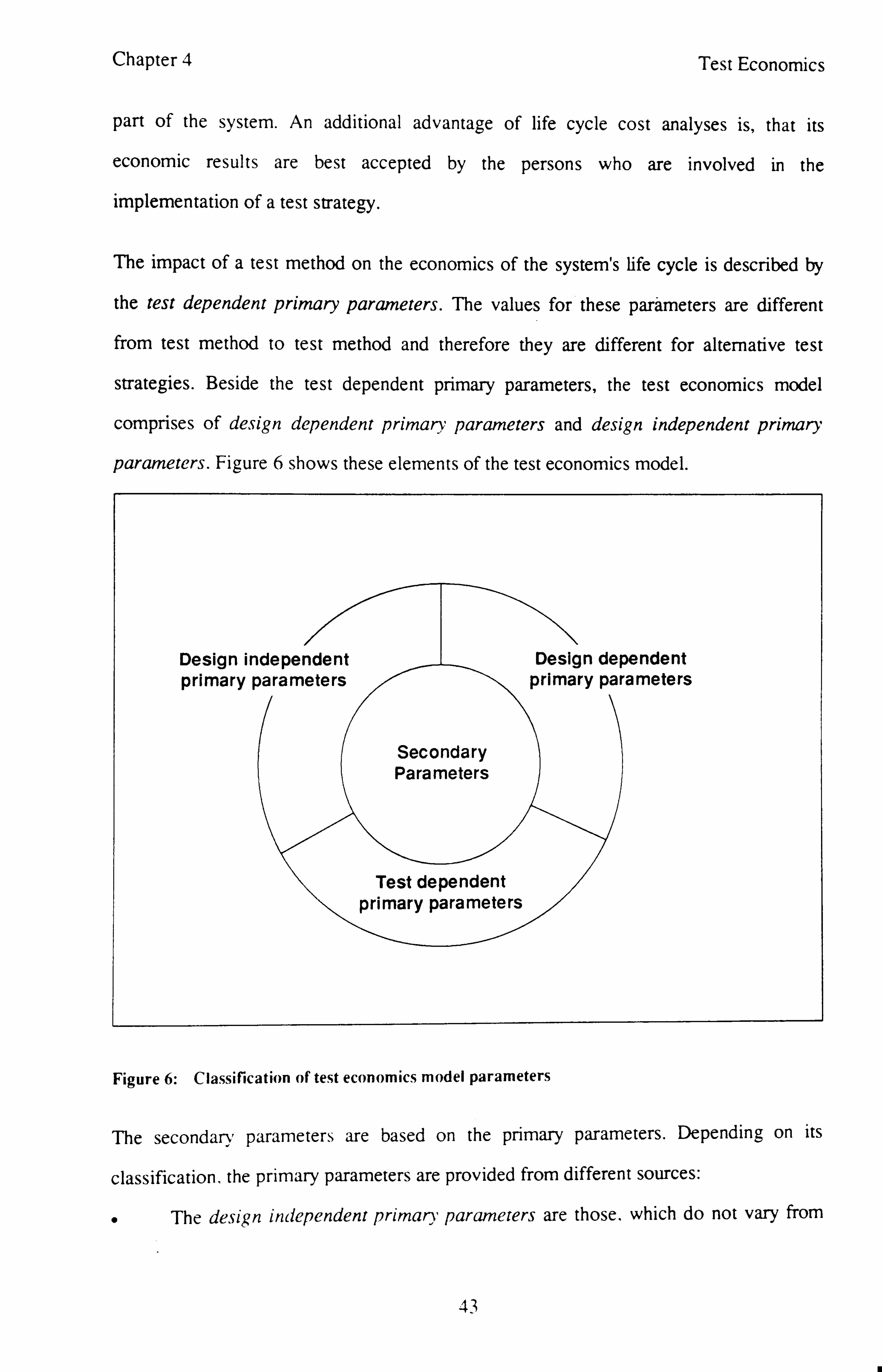
Chapter 4 Test Economics
part of the system. An additional advantage of life cycle cost analyses is, that its
economic results are best accepted by the persons who are involved in the
implementation of a test strategy.
The impact of a test method on the economics of the system's life cycle is described by
the test dependent primary parameters. The values for these parameters are different
from test method to test method and therefore they are different for alternative test
strategies. Beside the test dependent primary parameters, the test economics model
comprises of design dependent primary parameters and design independent primary
parameters. Figure 6 shows these elements of the test economics model.
Design independent primary parameters
Secondary Parameters
Test dependent primary parameters
Design dependent primary parameters
Figure 6: Classification of test economics model parameters
The secondary parameters are based on the primary parameters. Depending on its
classification, the primary parameters are provided from different sources:
0 The design independent primary parameters are those, which do not vary from
43

Chapter 4 Test Economics
design to design. Their values depend on the design environment (such as the
productivity of the CAD system used), or they are simply normalising factors.
The values of these parameters are stored in a data base, which can be updated
whenever the values change. The values are company specific and once they are
set, they will rarely change.
0 The design dependent primary parameters are those, which vary from design to
design and which are test independent (e. g. the production volume). Their values
are provided through a CAD interface.
" The test dependent primary parameters have been described earlier. Its values
are provided by test method dependent cost models. This means that for each test
method a separate cost model is developed, which calculates the test dependent
primary parameters from design dependent primary parameters and test method
dependent primary parameters. This means, that the structure of the entire
economics model depends on the test strategy, because parts of the economics
model depend on the test methods which are applied.
4.5. Structure of the Test Economics Model
The test economics model will be partitioned into several cost sections. The partitioning
process will be driven by two criteria:
" The life cycle of the system will be partitioned into several phases and sub phases.
The phases will be derived especially from a test view.
" The electronic system will be partitioned from the assembly and production view.
This means that every level of assembly will be represented by a separate cost
section with its own life cycle phases.
So the test economic,, model can be seen as a two dimensional model. One dimension is
the time (the life of the system), the other dimension is represented by the parts of the
system. In the following the author will describe the phases of the life cycle and the levels
of assembly.
44

%-f laNucc -+ Test Economics
The electronic system is built upon four levels of assembly:
The whole system includes all parts needed to perform the specified functions.
0 The system is composed of several boards. A board is defined as a module
containing several electronic components or sub-modules, which can be
assembled into one unit. The connection of boards within a system is
implemented by plug-in connections.
0A module is composed of electronic components. A module is simply a sub-
assembly of a board, and for the test economics model, it will not be seen as a
separate assembly level.
0A component is the smallest unit for assembly. Electronic components are
grouped into passive/active and digital/analog/hybrid. Digital components are
usually produced as ICs. In VLSI based systems, the essential components are
VLSIs. They may be designed in-house, and different test strategies may be
evaluated for them. Therefore a separate test economics model is developed for
VLSIs. The other components are assumed to be purchased, and only the
purchase cost per component are considered.
The test economics model is partitioned into the system level, the board level and the
component level, where the cost of each level are included in the model on top of it.
45

Chapter 4 Test Economics
Phases f
Sub phases Areas of cost origin
Production I Purchase, manufacture and assembly
Implementation
Test I Test, Diagnosis, Repair
Figure 7: Life cycle model for electronic systems with regard to test
Figure 7 outlines the phases of the life cycle of electronic systems. The partitioning into
sub phases was performed with regard to the impact of test strategies. The test
economics model can be simplified by neglecting those phases, which are not relevant for
the economic analysis. These are the initiative phase and the planning phase, because the
related tasks are performed before the test economics model is used, and therefore
related costs are not influenced by the test strategy. The phase-out phase does not
include test strategy dependent cost (see previous section), and therefore the related cost
can also be neglected for the test economics evaluation.
All other phases are considered for the test economics model. Some of the phases are
included at all levels of assembly. some of them are included only for a subset of the
assembly levels.

Chapter 4 Test Economics
4.6. A Life Cycle Test Economics Model for VLSI Devices and VLSI Based
Systems and Boards
The test economics model, which was developed by the author, is based on the structure,
which was presented in the previous section. Each level of assembly consists of a set of
cost models, which are related to the life cycle phases of the assembly unit. The author
has separated the costs occurring in the field from the other phases, because they occur
only for the entire system. The total cost per assembly unit is derived by the sum of cost
in the phases, and the total life cycle cost is derived by including the cost of lower levels
of assembly. The economic data needed in the model from a lower level of assembly are
grouped into three classes:
0 The volume related costs (VRC) are all expenditures which occur per device to
produce.
0 The non-recurring costs (NRC) are those expenditures which occur once per
product type.
0 The investments are all expenditures which can be shared with other products.
The following sections will describe the economics models per component, board,
system and in the field. A detailed description of the mathematical equations is given in
appendix B.
4.6.1. The Test Economics Model for ASIC components
The test economics for ASICs enables the prediction of all costs influenced by the test
strategy. The model fits for the development of cell-based ASICs. By cell-based ASIC's
the author means semi-custom ASICs, which are developed by using a cell library. A cell
library typically contains :
0 simple cells like and-gates or inverters
" more complex cells like counters or shift registers
0 macro cells like PLAs and RAMs.
47

Chapter 4 Test Economics
The model should be used by ASIC designers and their managers. Test strategy planning
should be done hierarchically in the same way as the design itself. Values for the
parameters which vary from design to design should be easily accessible, e. g. through a CAD data base. Initial effort is required for data gathering to derive the design
independent primary parameters. But the cost for daily use of the model should be
negligible. This was an important aspect of the model development.
The costs forming the model are divided into three parts:
0 The production costs are the costs of the VLSI supplier. These costs are not
calculated by a model, because the user of the model (this is the designer) cannot
influence the costs by controlling the production process. He has to pay the price
which is offered by the supplier, no matter what he would calculate by a cost
model. Nevertheless the price is influenced by characteristics of the design,
especially the gate number. A kind of data base as customer/supplier interface is
defined.
0 The design costs are the costs related to the design and development of cell-
based ASICs.
" The test costs are the costs related to testing purposes. These include the costs
for fault simulation and test pattern generation. ATE costs as part of the
production are only considered, if the ASIC price is influenced by the size of the
test set. Costs for an incoming test are usually related to board cost.
4.6.1.1. The Production Costs
The production costs are modelled by the detailed method (see 4.3). The risk of
predicting those costs is on the ASIC-supplier's side. He makes an offer, and the ASIC-
customer has to pay the offered price. Nevertheless this price depends on several
parameters. The values for these must be known, so they are part of the design
specification. The idea is to call for price offers for several sensible test plan
configurations. Several ASIC-suppliers confirmed, this would be possible. The
4

Chapter 4 Test Economics
production costs are also influenced by negotiations. The prices depend on particular
market interests of the supplier. If, for example, a supplier wants to secure business from
a company, he would probably start with low price offers. Also it is possible to have
more gates on the chip than predicted but not to pay more.
To get a price offer for a specific ASIC the supplier must have knowledge about the
following data :
Production Volume: Usually the volume is not one number. The expected delivery
volume has to be quoted for every year. Typically the volumes over five years are
predicted. For example, the prices can differ, if you have for the same ASIC a
production volume of 100,000, and the delivery is distributed in one case over
two years and in the other case over five years.
Complexity: The complexity is usually quoted in "number of equivalent gates". The
number is based on the equivalent gate number of the cells used. It usually
includes the gate number of the i/o-pads and excludes all macro cells. The
complexity of the macro cells is determined by their parameters (e. g. the number
of bits for RAM's).
Pin number: The number of pins has influence as well on the die size as on the package
size.
Number of Test patterns : Some suppliers limit the test set length. If the actual length
exceeds this limit, the customer has to pay more. This limit depends on the pin
memory size of the ATE.
Technology : Technology of the silicon.
Kind of Package : Package size and stock.
The chip price is composed by two different cost parts :
The non recurring engineering ('ARE) charges include all services from the supplier.
The NRE charges incur per design. What they really include depends on the customer-
vendor interface (see IArd871).
49

Chapter 4 Test Economics
The production unit costs is related to all costs incurred during the production of the
chip. They include the costs for silicon, package, wafer production, packaging and
testing. These costs are incurred per production unit. If there is a surcharge for long test
sets, this additional price is part of the test costs.
4.6.1.2. The Design Costs
The design costs depend strongly on the designers environment. Looking at some real
data about design schedules the author has found that the complexity of the design
cannot only be measured in terms of gates. The correlation between design time and the
number of gates to design is not very strong. The author supposes that in some cases the
Parkinson principle ("work expands to fill the available volume") is the most suitable
model for estimating design time. Nevertheless it should not be the aim of test economics
modelling to follow this principle.
The model must be used with the following assumptions :
0 The ASIC to be developed is a semi-custom design as described earlier.
"A top-down design by taking advantage of the hierarchical architecture is
assumed.
0 The CAD-system runs on a workstation. For workstations the CPU-time costs
are usually included in the engineer's cost-rate. If an outside design-centre is used
or some of the CAD tools run on a mainframe, these additional costs are drawn
explicitly.
The following design phases are taken into account for the prediction of design costs:
" Initial development of the circuit.
" Design capture.
0 Simulation and Verification.
The calculation of the design time is not only based on the gate count but also on other
design parameters and design environment parameters. The design parameters are the
t- IA

Chapter 4 Test Economics
gate count, the number of cells, the pin count, the originality of the design and the
performance criticality. The design environment or productivity parameters are the
productivity of CAD system which is used, the experience of the designers and the
productivity of the cell library, i. e. how well do the functions of the cells provided by the
cell library match to the actual design.
Test pattern generation and fault simulation are also part of the design process, but in the
test economics model the effort are considered as test costs.
4.6.1.3. The Test Costs
Test costs from [Var84] are composed of test pattern generation costs and test
application costs.
The test application costs amount to wafer test and component test. The wafer test and
the component test are part of the ASIC production. Test costs as part of the ASIC price
is usually constant. In some cases it is dependant on the test set length. A fixed number
of test pattern is included in the ASIC price and additional patterns have to be paid extra.
This extra price is step like. The steps depend on the pin memory size of the ATE. So the
extra price is part of the test costs, the basic test application costs are hidden as part of
the ASIC price.
The test pattern generation cost depend on the circuit, the fault coverage to achieve, the
performance of the test pattern generator and the type of test pattern generation
(sequential test pattern generation or combinational test pattern generation).
Deterministic test pattern generation can be performed by a tool (ATPG) or a person
(manual test pattern generation, MTPG). The generation of random test pattern causes
no test pattern generation cost. So the costs for test pattern generation for all self tests,
which are based on random pattern, are negligible.
Manual test pattern generation is done, where the ATPG system has problems, or where
an ATPG system is not available. Problems for ATPG systems usually occur having
51

Chapter 4 Test Economics
circuits with large sequential depth, and for asynchronous circuits. Especially for
asynchronous circuits MTPG is done in some cases. MTPG is done for the faults
uncovered by the test pattern from ATPG and the functional pattern used for the design
verification. It is also done for generating the propagation of patterns through the circuit.
The model for ATPG cost is based on [Goe8O]. The evaluation of data measured about
ATPG for scan-based circuits showed, that there is no significant correlation between the
CPU time and other circuit characteristics than the gate count.
Most of the ATPG systems for sequential circuits multiply the circuit for every time
frame. Therefore the effort on the average sequential depth of the circuits as well as the
number of gates.
The correlation of test pattern generation costs and fault coverage is also derived from
[Goe8O]. After reaching a fault coverage between 80% and 90 % very fast (exponential
shape, phase I), the curve becomes linear (phase II). This linearity is probably caused by
the fact that now most of the generated test pattern cover just a few additional faults. So
the slope depends on the fault coverage, where the slope becomes linear, and the
complexity of the circuit for test pattern generation.
4.6.2. The Test Economics Model for Boards
The test economics model for boards includes the two main phases "development" and
"production". Figure 8 shows a flow diagram of the phases.
S-)

J%C io (cCS ,
<. lidpLCU 4 Test Economics
Figure 8: Flow diagram of board level phases
The development phase includes the following sub phases:
" The design comprises of the initial design, design entry and computer simulation.
" The layout phase includes the placement and floor planning of the PCBs.
" The prototype manufacture covers the construction and manufacture of prototype
boards.
" In the verification phase the evaluation of the board by verifying the specified
functions with the prototypes.
" The test engineering phase covers the generation of test patterns, the generation
of the test programs and the manufacture of test tools, such as a bed-of-nails
fixture for an in-circuit test.
Due to the test view the production phase is partitioned into two sub phases:
0 The manufacture phase includes the production preparation, fabrication and
assembly.
1I
Development Production

`'"aN"` * Test Economics
" The test phase comprises of test application, which includes the costs for test, diagnosis and repair
In the test economics model structure the test engineering phase and the test phase are
combined into a single cost model because the cost structure of these costs is test
method dependent. For each test method a separate cost model exists, which models the
related costs for test engineering and test application.
The life cycle of a board includes a chance that a redesign may become necessary. This
can happen as a result of the verification or during the production phase. This fact is
considered in the test economics model by the definition of the probability of a redesign,
and by iteration factors per development phase, which define the effort needed for the
redesign as a percentage of the original effort.
The costs in the development phases include labour cost, equipment cost and material
cost. The labour costs are determined by the hourly labour rates and the predicted effort.
The equipment costs are related to computer equipment, which are needed for the
development of the design. They are also calculated by the hourly costing rates and the
estimated time, the equipment are needed. If the costs are included in the hourly labour
rates of the designers, the equipment costs can be set to zero. Material occur only for the
manufacturing of the prototypes.
The manufacture costs are composed of the production preparation costs, the material
costs and the assembly costs of the board. The material costs include also the total costs
for the components, which are calculated by the ASIC test economics model. The
calculation of the assembly cost is based upon the assembly cost per component and per
assembly type and the number of components per assembly type. In addition to the costs
the number of defects per defect type are calculated. These data are needed for the test
phase.
The test cost model includes the calculation of the test engineering costs and the test
54

,,, napter 4 Test Economics
application costs. The test engineering costs are composed of test tool manufacture costs
and test generation costs. The calculation of the test generation costs is based on the
engineering effort, the engineering labour rate, the usage of equipment and the
equipment rate. The test application phase is built upon the test phase and the diagnosis
phase as shown in figure 9.
from board production
repaired boards Test
Diagnosis and Repair
good boards
bad boards
Figure 9: The test/repair loop of the test application phase
The test is applied to all boards coming from production. The diagnosis and repair are
applied only for those boards, for which a defect has been identified during the test. All
repaired boards are retested, in order to detect multiple defects, and to detect defects,
which are injected during the repair.
In addition to the test and diagnosis/repair partitioning, the test economics model is
partitioned into four parts:
" In the quality model the fault coverage of the test is calculated, which is based on

k. napter 4 Test Economics
the fault spectrum of the previous stage. Depending on the test strategy, the
previous stage can be the manufacture phase or another test phase.
" The time model calculates the total times for test application, diagnosis and
repair, depending on the times per board and the number of boards going to test
and to diagnosis/repair.
0 The cost model calculates the actual financial cost. This includes the procurement
of test equipment and the usage of these test equipment, and the labour costs for
the test personnel. In addition the repair costs are calculated. These are based on
the labour costs and the material costs. For the calculation of the material costs
the type of the defect is taken into account.
The times and the financial costs are calculated for the test phase and the diagnosis and
repair phase.
4.6.3. The Test Economics Model for Systems
The test economics model for electronic systems includes the phases development,
production and field usage. The field usage will be described in the next section. This
section describes the economics models of the development phase and the production
phase of the system.
In the area of the system development only the test engineering costs are relevant for the
test strategies. The test strategy dependent development costs are mainly related to the
board development and the component development, and the related costs are included
in the total system costs as part of the total board costs. The test engineering costs are
combined with the test application costs in the same way as for boards.
The production cost model of the system includes the costs for the assembly of the
boards into a system, the total costs of the boards and optional device costs for
incorporated test devices, which support the test and diagnosis of the system in the field.
The system test costs comprises of test engineering costs and test application costs in the
56
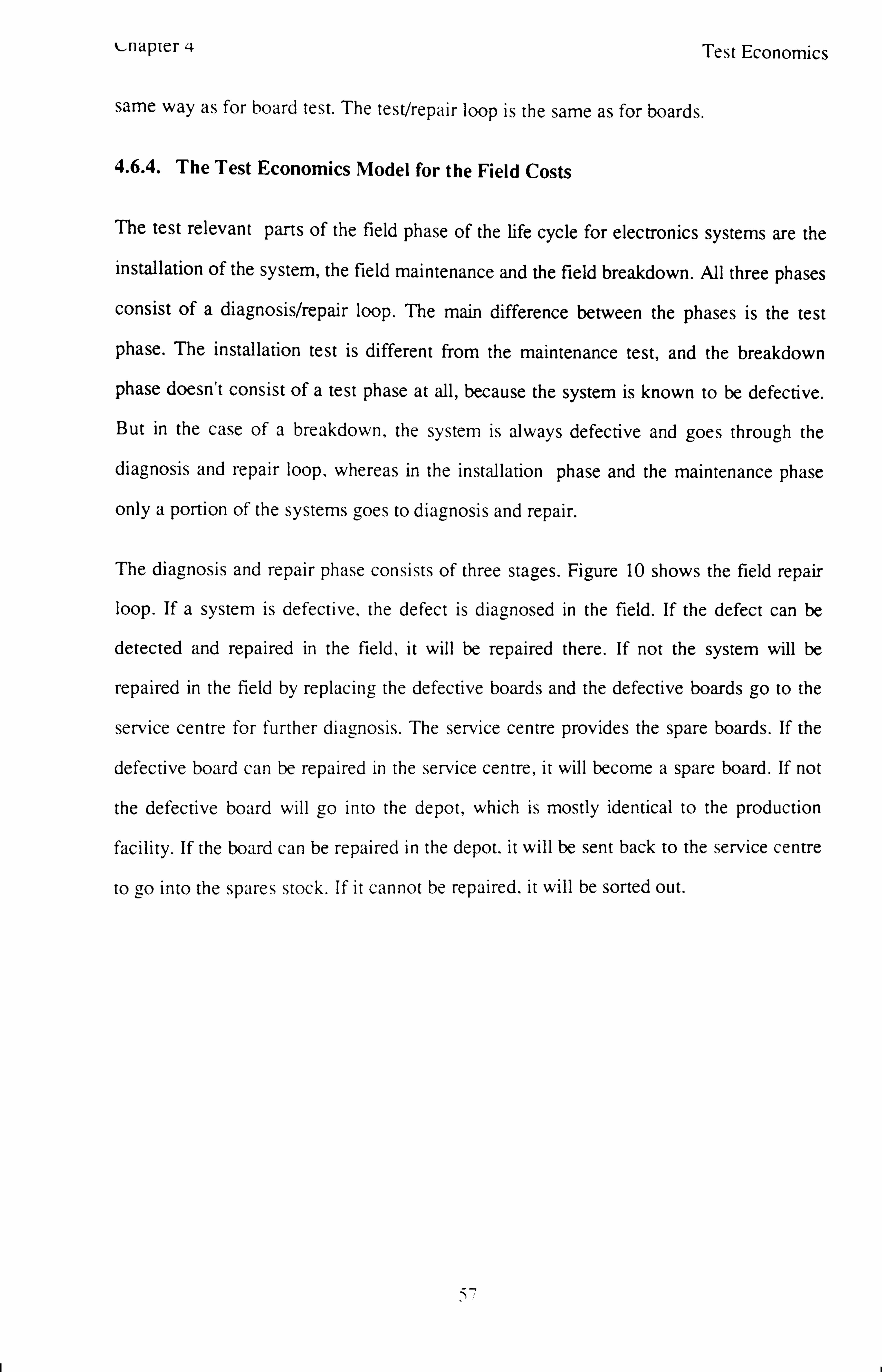
w. napter 4 Test Economics
same way as for board test. The test/repair loop is the same as for boards.
4.6.4. The Test Economics Model for the Field Costs
The test relevant parts of the field phase of the life cycle for electronics systems are the
installation of the system, the field maintenance and the field breakdown. All three phases
consist of a diagnosis/repair loop. The main difference between the phases is the test
phase. The installation test is different from the maintenance test, and the breakdown
phase doesn't consist of a test phase at all, because the system is known to be defective.
But in the case of a breakdown, the system is always defective and goes through the
diagnosis and repair loop, whereas in the installation phase and the maintenance phase
only a portion of the systems goes to diagnosis and repair.
The diagnosis and repair phase consists of three stages. Figure 10 shows the field repair
loop. If a system is defective, the defect is diagnosed in the field. If the defect can be
detected and repaired in the field, it will be repaired there. If not the system will be
repaired in the field by replacing the defective boards and the defective boards go to the
service centre for further diagnosis. The service centre provides the spare boards. If the
defective board can be repaired in the service centre, it will become a spare board. If not
the defective board will go into the depot, which is mostly identical to the production
facility. If the board can be repaired in the depot. it will be sent back to the service centre
to go into the spares stock. If it cannot be repaired, it will be sorted out.
1ý

%-IidpLC; l Test Economics
Figure 11: Field repair loop
From this scenario the following cost models are developed:
0 The field usage cost model consists of field installation, field maintenance and
the field repair costs. This includes the defect rates of the system to be installed,
the defect rates of maintained systems and the mean time between failure in order
to calculate the breakdown rate. The number of systems, which cannot be
repaired in the field, is determined from the field repair rate, and the number of
boards, which are going to the service centre is derived from the average number
of boards which are replaced at one failure and the number of failures.
0 The service centre cost model includes the costs for the provision of spare
boards and the repair costs for the boards, which are actually repaired in the
service centre. The number of spare boards which are needed takes into account
the time needed to repair a defective board.
0- The depot cost model includes the repair costs for the boards and the production
of new spare boards. which are needed due to the sort-out of non-repairable
58

Lnapter -+ Test Economics
boards. The number of non-repairable boards is derived from the total number of
boards going to depot repair and the percentage of boards which are not
repairable.
4.6.5. Consideration of Interest Rates
Interest rates can be an important factor, if the time for return-of-investment is
considerably long and if the market interest rates are significant. Therefore the costs for
the early development phases differ from the same costs in the production. The following
example should make this fact clear:
The total development time of a system takes two years. The market interest rate is
constant at 12%. The initial design is performed at the beginning of the development
phase, and the test program generation is performed at the end of this phase. For
simplification, these two phases are assumed to be very short compared to the total
development time. The costs for both phases is £10,000. To compare these two costs,
they must be related to the same time point. We take the end of the development time as
the common time point. This means, that considering the interest rate impact, the
£ 10,000 for the test engineering phase remain unchanged, whereas the £ 10,000 for the
initial design become £2,544.
So, expenditures which are made early are more expensive as the same expenditures,
which are made later. This fact can be important for test strategy planning, if the interest
rates are high and two test strategies differ in expenditures which have to be made at
significantly different times.
For that reason the author has included the interest rate aspect. All costs are converted
to a common time point. which i,, the end of the life cycle. This is done by using the
present value method (Blo88 ].
59

%-, napter 4
4.7. Summary
Test Economics
This chapter presented economics modelling techniques and their uses in test economics
modelling. The impact of test strategies on the economics of electronic systems during
the life cycle of the system was described and discussed. The test economics model
which was developed by the author was described. This test economics model will be
used for test strategy planning in order to evaluate the economics of test strategies. The
author has developed methods and advisory software systems for supporting this test
strategy planning task. ECOTEST is a test strategy planning system for ASICs, and
ECOvbs is a test strategy planing system for VLSI based systems. These two systems
and underlying methods and algorithms will be described and discussed in the following
three chapters.
60

k. napter
Chapter 5
ECOTEST
5.1. Introduction
ECOTEST
ECOTEST is a test strategy planner, which is an enhancement of the EVEREST test
strategy planner [Dis92]. The author has enhanced certain parts of the EVEREST test
strategy planner, which were identified to be weak. But most of the concepts remained
unchanged.
The development of the EVEREST test strategy planner was a collaborative project
between Brunel University and Siemens-Nixdorf. The author has developed many
concepts, which are implemented in the EVEREST test strategy planner, and he has also
developed major parts of the software. The EVEREST test strategy planner is described
in detail in [Dis92]. This chapter will concentrate on how ECOTEST is integrated into a
test engineering environment, and on the testing philosophy behind ECOTEST. The
complete system will be described as an overview, and the enhancements of ECOTEST
against the EVEREST test strategy planner will be described in detail.
Previous work in this area has mainly been addressed in [Aba89], [Dis9l] and [Laf91].
TIGER [Aba891 performs test partitioning and test plan generation in addition to
automatic test strategy planning (ATSP). The aim is to make a design testable and stay
within certain design limits such as area or test time. However the cost measures adopted
to drive the search for the best test strategy are based on different measure units. For that
reason they cannot be evaluated against each other. ITSELF [Laf9l ] is a system to check
the applicability of test methods. which is an important task when the large variety of test
methods is considered. but does no selection, if several solutions are possible. The
system only checks whether the design and test constraints are met. The work at Brunel
University in this field began with the development of a test economics model [Var84],
where design-for-testability methods like scan path or self test were studied under
61

unapter 5 ECOTEST
economic aspects. The advancements of this work resulted in the test strategy planning
system BEAST [Dis92]. In BEAST, the decision process of selecting test methods test
methods is driven by the economics of its application. This means, that the selected
combination of test methods (the test strategy) should be the cost optimal solution. In
the joint project with Siemens-Nixdorf a new test economics model (see chapter 4) was
developed and included in the EVEREST test strategy planner([Dis9l], [Dis92]).
ECOTEST is an enhancement of the EVEREST test strategy planner.
The scope of ECOTEST is to find the most economic test strategy for a given design,
which fulfils all the technical constraints. Other systems (e. g. [Aba891) limit the search
space by setting for example area and test time constraints. Such limitations are normally
supplied by the designer. In addition to the limitations, user defined weights are used in
order to allow the comparison of different parameters. This comparison can then be used
to select a test strategy among the ones which meet all constraints. But the final selection
depends on the objectivity and experience of the designer in weighting parameters which
are not always directly comparable. This fact may lead to non optimal solutions. For that
reason, the EVEREST test strategy limits the user defined restrictions to technical
constraints only, while cost related parameters are compared using the test economics
model. This provides a common reference point for all cost related parameters, which
can therefore be compared objectively.
In the following section the philosophy of ECOTEST will be described. In the rest of this
chapter the usage of ECOTEST in a test engineering environment will be described and
discussed, the EVEREST test strategy planner, which is the basis of ECOTEST, will be
outlined, and the enhancements of ECOTEST against the EVEREST test strategy
planner will be described and discussed.
5.2. The Philosophy of ECOTEST
Today's IC technology allows to integrate different types of circuits on one chip. A
typical VLSI of ASIC consists not only of random logic, but contains also other design
62

Chapter 5 ECOTEST
methodologies such as RAMs, ROMs, PLAs and complex macros as e. g. microprocessor
cores, data paths, or multipliers. Some of these blocks are created via logic synthesis,
silicon compilers or module generators, others are predefined macros. Due to the variety
of structures and functions on such an IC, this type of circuits is called heterogeneous
circuit. In order to keep the costs of testing of chips within reasonable bounds, a variety
of design-for-testability methods have been developed. Most of the advanced design-for-
testability are optimised for a specific class of circuits. Especially for RAMs and PLAs a
large variety of DFT methods have been developed and published. For example, in
[Zhu88] about 20 DFT methods for PLAs are presented. The heterogeneity of the
circuits and the variety of DFT methods have led to the idea of modular testing or macro
testing ([Bee90], [Rot89]). This method allows the use of different test methods and
DFT methods for different parts of the circuit. The independently tested parts are called
testable units. For every testable unit, a different DFT method can be applied. In the
macro test methodology [Bee90] is coupled to a silicon compilation approach, and the
testable units are related to the functional macros which are generated by a silicon
compiler. The modular test methodology does not link the testable units, which describe
the test hierarchy. to a certain design hierarchy. Therefor the testable units can be
selected by minimising the related costs.
In ECOTEST, we have adopted this modular test approach. The test hierarchy is defined
by the netlist hierarchy. The netlist hierarchy can be provided by a test partitioning tool,
or by the designer. Different test hierarchies may be evaluated in order to find the cost
optimal solution.
A test method describes a procedure, which includes a DFT method, a test generation
method and a test application method. A test application method always includes a test
pattern driver and a test response receiver, which are called here the test resources. In
the case of an external test. these are represented by the chip inputs and outputs. In the
case of BIST, the test resources are represented by the BIST logic. A testable unit is
defined as a part of the circuit. which is homogeneous respecting the design
63

Chapter 5 ECOTEST
methodology, and to which a test method is applied. The testable unit must be accessible by the test resources of the test method to be applied. This accessibility can be achieved
through transfer paths in the circuit, or through additional DFT logic. In ECOTEST, this
additional DFT logic is called external test method, whereas the test method to test the
testable units is called internal test method.
The objective of test strategy planning in ECOTEST is to find the most economic test
strategy for the target design with a given test hierarchy. By varying the test hierarchy,
the user can evaluate the impact of different hierarchies on the economics of the test
strategies.
This leads to the way ECOTEST should be used. ECOTEST is a testability advisor,
which advises the designer in how to create a design, which is testable by minimum total
expenditures. This creation of a testable design is called test strategy. The test strategy is
the specification, which testable unit is tested by which test method. So the decision on a
test strategy includes the decisions about the design methodology (DFT), test generation
methodology and the test application methodology. From these decisions, the first to be
made is the design decision. The point of time, when this decision must be made,
depends on how deeply the DFT method is integrated into the functional design. For
some DFT methods, such as all scan design techniques, the decision must be made,
before the design starts, i. e. during the specification phase. But the answer to the
question, which scan design technique is the best, may be left until the functional design
is completed. This late decision is advantageous, because the data, on which the test
strategy decision is made, i. e. the costing parameters of the test economics model, are
more accurate in this phase. For that reason ECOTEST should be used in two phases of
the design:
0 In the design specification phase. ECOTEST should be used in order to make
sonne general decisions, such as whether synchronous design is required or not,
or whether a scan design will be implemented or not, i. e. all decisions which
affect the functional design of the circuit.
64

Chapter 5 ECOTEST
0 After the completion of the functional design, the detailed test strategy planning
should be performed. This includes the decision on what scan design, what kind
of self test, or what test hierarchy is optimal. During this phase most of the
costing parameters are known very well. For example, parameters such as the
gate count or the number of flip flops can be extracted from the netlist
description instead of predicting them. In addition, simulation tools can be used,
which simulate a certain DFT condition in order to derive parameters such as the
number of test patterns, or the achievable gate count. Such simulation tools have
been developed , and they can be linked to ECOTEST. For example, the test
pattern generation system TENsocrates[TEN91 ] includes a preview mode, which
simulates a full scan path for a given design, and generates test pattern for it in
order to derive the number of test patterns and the achievable fault coverage as
main costing parameters. Or the BIST advisor TENstar [Bar92] simulates several
self test methods for a given design in order to derive the achievable fault
coverage and the number of test patterns. By linking these tools to ECOTEST, a
very accurate economic analysis can be performed.
The local application of a test method to a testable unit may have global implications to
the design, which will affect the test economics of the whole design. These implications
result from accessibility implications, which will affect the accessibility of other TUs, the
exceeding of technical constraints, the sharing of test pins between TUs, the shareability
of test resources. and the nonlinear behaviour of costing functions.
A local test method application can affect global accessibility, due to transfer of data to
neighbouring TUs. If a TU is made accessible through a test method, all ports of the TU
become accessible. and therefore also all ports. which are connected to ports of the TU
under consideration. If such a port is part of a block, which is capable of transferring the
data, e. g. a multiplexer, or a register, other ports also become accessible through that
transfer function under certain conditions. These conditions are the controllability of this
transfer function. For example. a multiplexer can transfer data in a controlled way only, if
65

Chapter 5
the control line of the multiplexer is accessible.
ECOTEST
If a test method application implies the need for additional test pins, the same pin may be
used for several test methods applied to different TUs.
If a technical constraint such as the maximum number of pins is exceeded, this exceeding
may result from additional pins which are needed for different test methods which are
applied to different TUs. So, the application of a certain test method to a certain TU may
exceed this global limit, but the exceeding is not directly related to this application but to
the application of all test methods which need additional pins.
Self test methods often use a special logic to generate test patterns and to evaluate the
test responses online. This logic is called test resource. These test resources can be
shared between TUs. Figure 12 shows an example for the shareability of test resources.
TU I TU2
APPLY BILBO APPLY BILBO B
TU 1LL TU2 B B- 0O
share test resource B
TU 1L TU2 B 0
Figure 12: Shareability of test resources
Assuming, that the test method BILBO [Koe79] would be found to be the best test
method for TU I and TU?, the test method application procedure would require for each
TU a BILBO register at the inputs and the outputs. Due to the fact, that the outputs of
TU I drives the inputs of TU?, the BILBO register at the output of TU I can be easily
shared with the BILBO register at the input of TU2.
66

%-IlapLci J ECOTEST
5.3. ECOTEST in a Test Engineering Environment
ECOTEST as an advisory tool should be used in combination with other test engineering
tools, which support the implementation of the selected DFT methods, and which
support or automate the generation of test plans, test patterns and test programs. The
variety of test methods strongly depends on the availability of such tools. For example, it
makes no sense to select a scan design test strategy with automatic test pattern
generation (ATPG), if no ATPG system is available. Also, ECOTEST should be totally
integrated into the CAD system, which is used, in order to provide data such as the
netlist, or cell library data. The following links between CAD tools and other test
engineering tools should be incorporated:
" ECOTEST should be linked to the CAD system by a netlist interface, a functional
interface and a cell library data interface. The netlist interface should provide all
data about the test hierarchy, i. e. which are the testable units, the type of the
testable units (e. g. RAM, combinational random logic, sequential random logic),
and the structure of the design. The functional interface should provide the
information about the data transfer properties of the testable units. And the cell
library data interface should contain per cell data like the size (in equivalent gates,
in mm1) , or in bits for RAMs) or the number of basic storage elements (e. g.
number of flip flops).
0 ECOTEST should be linked to tools which derive costing parameters, or which
analyse the design concerning testability characteristics. These tools include
advisory tools as mentioned in the previous section, testability synthesis tools
such as partial scan selection tools ([Tri83], [Che89], [Gun90]), and tools, which
analyse the accessibility of the testable units, such as SPLASH [Keu93].
0 The test method data base of ECOTEST should take into account the availability
of test methods due to the availability of test generation tools and testability
synthesis tools. The economics of a test method strongly depends on tools which
support this test method, in terms of automatic test pattern generation as well as
67

Chapter 5 ECOTEST
in terms of testability hardware synthesis.
These aspects are considered in ECOTEST through its interfaces, which allow to access
the data coming from other tools. ECOTEST comprises of an EDIF netlist interface,
which provides integrity to nearly all CAD systems on the market. It consists of a cell
library data interface, which allows to access automatically data about the complexity of
the testable units. The data transfer characteristics of the testable units are accessed
through an interface, which was introduced by Philips [Bee90]. And the test method
descriptions are provided such that the user can maintain the data in order to adapt them
to its own environment.
5.4. The EVEREST Test Strategy Planner
5.4.1. The Data Interfaces
Figure 13 shows the architecture of ECOTEST. ECOTEST uses the following data
interfaces:
68

Lnapter ECOTEST
Figure 13: The ECOTEST architecture
The netlist provides the data about the structure of the circuit, the definition of the
testable units, and a classification of the input ports of the testable units. All cells, which
are part of the top level cell, i. e. the main circuit, are considered as testable unit. The
type of the testable unit is defined by a property entry. Cells, which are defined on that
level, but which should not be considered as testable units, such as pin driver cells in a
standard cell design. can be classified as no testable units by a specific property class.
The format of the netlist is EDIF.
The transfer description provides the information under which conditions test data can
be transferred through a testable unit.
The cell library data file contains the complexity data of the cells in a cell library. This
complexity data include the equivalent gate count and the number of storage elements for
random logic cells, the number of bits for RAMs or ROMs, and the number of product logic
lines for PLAs. ECOTEST comprises of a function, which automatically calculates the
69

Chapter 5 ECOTEST
equivalent gate count and the number of flip flops per testable unit, by using the cell library data, and analysing the netlist structure, which is based upon the cells of the cell library, for each testable unit.
The production unit cost file provides a pricing table for the IC, which is based upon
the gate count, which defines gate count ranges, in which the price increase of the IC is
linear, or in which the price is constant, e. g. for gate arrays. Based on this table the
production unit costs can be calculated for the related gate count.
The design description includes all netlist data and all economic parameters of the
design, which are needed to make an economic analysis of test strategies. The design
description is generated by ECOTEST, and it is based on data provided by the netlist
interface, the transfer descriptions, the cell library data, the production unit costs data,
and data which are provided by the user through the user interface.
The cost model template is the basic cost model. This is design independent, and it
contains the general secondary parameters, the templates for secondary parameters,
which occur per testable unit, and templates for all primary parameters. The cost model
consists of primary parameters and secondary parameters. The primary parameters
provide the input values to the cost model, and they are classified into three groups:
0 The design dependent primary parameters are those, which do not vary from
design to design. Their values depend on the design environment (such as the
productivity of the CAD system), or they are simply normalising factors (such as
normalising the values to the currency which is used). These parameters are
company specific and once they are set, they will rarely be changed.
" The desii'n dependent primary, parameters are those, which vary from design to
design. but which are test independent (e. g. the production volume). Their values
are extracted from the design description.
" The test dependent Primary parameters are those, which vary from test strategy
to test strategy. Their values are calculated in separate cost model, which are
70

1-napter ECOTEST
defined in the test method descriptions, and these parameters are linked to the
related test method descriptions, depending on which test method is applied to
which testable unit.
The secondary parameters form the cost model kernel. These parameters are set to
equations, based on either primary parameters or previously calculated secondary
parameters.
Based on the cost model template and the design description which contains the
information about the testable units and the primary cost model parameters, the cost
model is automatically generated by ECOTEST. All parameters which are defined per
testable unit, such as the gate count, are expanded to the correct number of testable units
by extending the name of parameter by the name of the testable unit.
The test method descriptions provide all the information about test methods which is
needed to perform test strategy planning. This includes the suitability of the test methods
for the particular testable unit, basic design implications of the test method application,
and a cost model, which defines the test dependent costing parameters as a function of
the design parameters. The design implications are the type of the test method (internal
or external, self test or not), a pin compatibility class and the accessibility implications.
The pin compatibility class defines the shareability of the additional pins between the test
methods of different testable units. The accessibility implications define, whether the
accompanied test method provides accessibility to the inputs or outputs the testable unit,
to which it is applied. The test dependent parameters are:
" The gate count.
0 The number of cells.
" The design originality.
" The performance impact.
" The number of additional input pins, output pins and bidirectional pins.
" The number of test patterns per test pattern type. The test patterns types are
71

%., ºlapLci .) ECOTEST
normal test patterns, self test patterns, scan test patterns. The test equipment may
handle these test pattern different, and therefore the test application costs may be
different for the different test pattern types.
0 The achievable fault coverage.
0 The test pattern generation cost.
These parameters are described in formulas in the same syntax as the cost model. The
formulas are based upon the design parameters. The test dependent parameters are used
as input parameters of the cost model.
The test strategy file is generated by the ECOTEST, and it contains the definition of the
final test strategy and the values for all costing parameters.
5.4.2. The Functions of ECOTEST
ECOTEST comprises of four functional blocks:
The design specification reader (DSR) prepares the netlist data and the other design
related data for the internal design representation and creates the design description file
and the design specific test economics model (the cost model). It allows to modify the
cost related data of an existing design description.
The cost model (CM) contains the knowledge base about the cost relations of the
design. This functional block includes the parsers of the cost model file and the test
method related cost models, the building of the internal cost model structure, the
evaluation of the cost model, the printing of the cost model parameters, and a sensitivity
analysis for a single parameter by varying this parameter and calculating the impact of
this variation on another parameter of the cost model.
The test strategy, planner (TSP) evaluates the economics of the test strategies by using
the test method descriptions, the cost model and the design description. The test strategy
planner allows interactive test strategy planning as well as automatic test strategy
72

Chapter 5 ECOTEST
planning. Therefore it provides the following functions:
0 Various automatic test strategy planning functions are provided. These enable
automatic test strategy planning of the whole design, of single testable units
(TUs), automatic test strategy planning to make the TUs accessible and
automatic test strategy planning without making the TUs accessible.
" Interactive test strategy planning can be performed by using a function, which
applies a user defined test method to a user selected TU.
0 The accessibility function calculates the accessibility of the input- and the output
ports of the testable units. The calculation is based upon the netlist, the transfer
functions of testable units, and on accessibility enhancing characteristics of the
test methods, which are applied to the testable units.
0 The test method descriptions are parsed and provided for the test strategy
planner.
0 The applicability of a test method is checked, before it is applied. This includes a
check of the suitability of the test method to the type of the TU (e. g., for RAMs,
only RAM test methods can be applied), and a check of the violation of
constraints. the constraints are user defined, and they include a maximum gate
count, a maximum pin count, and a maximum self test time.
The user interface is implemented as a command handler system, and it provides four
different command handlers:
" The ECOTEST handler includes general commands for data handling and for
maintaining the handler.
" The DSR handler provides several commands fro the set up and modification
of design data.
" The TSP handler provides commands for the modification and handling of test
strategies. L
" The PRINT handler provides several print commands.
Table 4 provides a list of all commands,. which are implemented in ECOTEST.
73

ECOTEST
Command name Description ECOTEST handler alias define a new command enter enter another command handler shell execute a shell command echo print a message read read commands from a file help p rints a list of available commands together with a brief description mod startup modify the startup file quit terminate the execution of ECOTEST DSR handler global modify global costin data tu modify TU related costing data trans modify transfer functions of TUs si class modify type of input ports of the TUs sigwidth modify the bundle width of ports and nets TSP handler apply apply a test method to a testable unit atsp execute automatic test strategy planning, either for the whole circuit or for a
specified block
ats ext execute automatic test strategy planning only for making all TUs accessible ats int execute automatic test strategy planning without making the TUs accessible set set a parameter to a certain value reset reset all parameters to initial values calculator start the X11 graphical calculator save is save the test strategy for later reload or for comparisons to other test strategies reload is reload a previously stored test strategy delete is delete a previously stored test strategy Ls-history print a previously stored test strategy PRINT handler
cm print cost model parameters tu print TU related cost model parameters Ls print test strategy
table execute sensitivity analysis and plot the related curve on screen
access print non-accessible input and out ports of the testable units circuit print design data
tmdhelp print a user friendly description of test methods on screen Table 4: Commands of ECOTEST
The implementation of ECOTEST is based on the EVEREST test strategy planner. The
DSR functions remained nearly unchanged. The cost model and the user interface are
completely new. The accessibility' function of the test strategy planner and the automatic
test strategy plannin`_ al<_orithmý, remained unchanged. The rest of the test strategy
planner is completely new.
Where the EVEREST test : trate, \ was written in C. ECOTEST is a mixture of C and
74

%-napter ECOTEST
C++. All parts which were taken from the EVEREST test strategy planner are in C,
whereas all new functions are implemented object oriented in C++.
The concepts which were taken from the EVEREST test strategy planner were developed in a collaborative project. The concept and the implementation of the design
description was developed by the author. The concept of the accessibility functions was
jointly developed between Brunel University and Siemens-Nixdorf. All the new concepts
and functions implemented in ECOTEST have been developed by the author.
The next section will describe the concepts of the cost modelling techniques and the test
strategy planner which have been implemented in ECOTEST. Both concepts are object
oriented, which makes the methodologies very flexible and its applicability very general.
5.5. Cost Modelling Techniques
The cost model evaluator calculates the costing parameters, which are based upon the
input values. The calculation rules are defined by the operators and the order of the
parameter definitions.
The cost models are represented by a directed graph. Each operation is represented by a
node, and the edges represent the links to the operators of the operation. Figure 14
I1LS dll CXd[IIUIC cost IIIVUCI.
b=2 c=3 a= b+c+4
Figure 14: Example of a cost model and its internal representation
75

Chapter 5 ECOTEST
Each parameter and each operation are represented by a node. An assignment operator does not create a new node but adapts the parameter name to the assigned term. Each
operation node includes a list of operators, which are implemented as pointers to the
related nodes. Input nodes are those which do not perform an operation, but which are
provided with a certain value. Needless to say, that the input nodes do not have any
operands. The nodes are implemented as C++ classes with a inheritance hierarchy. The
generic opnode class includes the name of the parameter, the list of operands, the list of
the users of the node (backward pointer) and the value. In addition, it provides several
functions print or to read the name and the value. For each operator, a class is
implemented which inherits all data and functions of the opnode class. These operator
classes do not provide any data but do provide the calculation function which is specific
to the type of the operation. Input nodes also inherit the functions and data of the
opnode. In addition, they consist of the input value and the calculation function, which
assigns the input value to the parameter value. A special connect node is provided for
input parameters, which are connected to a parameter of another cost model. This class
provides a pointer to the related parameter, and a calculation function which reads the
value of the related parameter and assigns it to its own value.
All nodes of a cost model are stored in an ordered list. The ordering criteria is the order
in which the nodes must be calculated. The calculation of the complete cost model is
then performed by calculating the nodes of the ordered list. An alternative to this method
of calculation is a recursive calculation of each node, starting with the last parameter in
the cost model. But in the case of reconvergencies of the graph, this method would lead
to multiple calculation of some of the nodes, which reduces the performance of the cost
model calculation. Reconvergencies occur. when a parameter is used in more than one
term.
The ordered list is part of the class graph, which provides in addition to the ordered list
of nodes several functions to create the ordered list, to find a single node in the list, to
calculate the list. and to print the data of the nodes.
76

Chapter 5 ECOTEST
The class cost_model is itself a node, which means, that it inherits all data and functions
of the class opnode. This allows to handle the hierarchical cost model approach, where a
cost model may be built upon several sub cost models. The cost model class contains the
following data and functions:
0 the graph with all nodes, which are part of the cost model.
0a list of user parameters, which is a subset of all nodes, and which are visible to
the user.
" the list of input parameters, which is a subset of all nodes.
"a function to parse the cost model file and to create the cost model graph.
0 several functions to access parameters and parameter data of the cost model.
0a function to connect input parameters of the cost model to parameters of
another cost model.
0a function to calculate the cost model.
The cost model parser was implemented by using the UNIX tools LEX and YACC.
These tools are very efficient in parsing files with a certain syntax and for describing a
certain grammar. The software module, which is automatically generated from a YACC
description, delivers the nodes of the cost model in the right order, so that an explicit
ordering of the nodes is not needed.
The method described above for representing and calculating cost models is very
efficient. The calculation time is about 200 times faster than the method implemented in
the first version of ECOTEST (see [Dis9? ]) and only about 10 times slower than a hard
coded cost model. A hard coded cost model is an implementation in which the cost
model equations are part of the source code. This makes the cost model calculation very
fast -a further improvement could only be achieved by a hardware accelerator - but
inflexible concerning cost model modifications. The author's approach is an efficient mix
of flexibility and performance.
Some of the design parameters are test method dependent. The test method dependent
77

Chapter 5 ECOTEST
parameters are the number of not accessible input ports, output ports and bidirectional
ports per testable unit. These parameters are used by the external test method cost
models. They use these parameters in order to calculate the parameters, which depend on
how many ports need to be made accessible. In the case of an external scan path, the
number of flip flops to be included, and consequently cost model parameters like the
additional gate count, depends on how many ports of the related TU are not accessible
yet and need to be made accessible. As discussed earlier, the accessibility of ports
depends also on the test methods which are applied to other TUs. Therefore the number
of non-accessible ports of a TU is test strategy depend, and needs to be recalculated with
each test strategy. In ECOTEST these three parameters are implemented as functions,
which means, that the related value is calculated by calling a C-function. This function
calculates the accessibility of the TU and returns the related number of non-accessible
ports.
In the same way, the number of pins is calculated. A special function calculates the
number of input pins, output pins and bidirectional pins. The algorithm to calculate the
pin numbers is as follows:
set number of pins to number of pins without any test method for each pin compatibility class do
select all applied test methods which match to the pin compatibility class add the maximum of the additional pins from the selected test methods to the number of pins
end do
The test strategy planner is also modelled as a cost model, and it contains the blocks of
figure 16 as nodes. The test strategy planner is described in the next section.
5.6. The Test Strategy Planner
In ECOTEST. the test strategy planner is a cost model with some additional attributes
and functions. In the object oriented language, this means, that the test strategy planner
is a class which inherits the class cost model. This means, that it inherits all functions and
78

`, uapLcr J ECOTEST
data attributes of the cost model, such as the calculate function, the print function, or the
ordered list of nodes to be calculated. But in the test strategy planner class, the functions
have a different implementation.
The calculation of the total cost for a given test strategy is the objective of the
calculation function of the test strategy planner. This calculation is based on the main
cost model, on the test method cost models of the applied test methods, and on the
design parameters, which are linked to the input parameters of the cost models. Figure
15 shows the structure of the test strategy planner cost model. This example shows the
structure for a design with three testable units, TU1, TU2 and TU3.
The list of nodes in the test strategy planner is fixed. It contains the design parameters,
which are a cost model and therefore a node, the testable units, which are also nodes, the
pin calculation cost model and the main cost model.
The list of nodes of the testable units consists of the internal and the external test method
cost model, which are applied to the testable unit. This means, that the testable unit as a
cost model changes, when one the two test method changes, i. e. if a new test method is
applied to the testable unit. In addition to the cost model attributes and functions, the
testable unit contains a list of all applicable test methods, from which the user of the test
strategy planner selects the test methods to be applied.
The internal test method cost model is based on the design parameters, and the external
test method cost model is based on the design parameters and the test dependent
parameters of the internal test method cost model.
The calculation of the number of pins is based on the original number of pins, the
additional number of pins from the test method applications and the pin shareability
conditions of the test methods, which are applied.
The calculation of the main cost model is based on the design parameters, which provide
the values for the design dependent primary parameters, the external test method cost
79

Chapter 5 ECOTEST
models per testable unit, which provide the values for the test dependent primary
parameters, and the pin calculation cost model, which provides the total number of input
ins, output pins and bidirectional pins.
Design Psnmetws
IMem. I
TU1 Test Method
Internal
TU2 Test Method
IMsmd
TU3 Teat Method
External Test Method
ExtemM Test Method
External Test Method
Number of Pins
Main Cost Model
Total Cost
Figure 15: Structure of the cost model calculator
Beside the attributes and functions of the cost model, the test strategy planner includes
further attributes and functions. The most important functions will be described
subsequently.
The methods for automatic test strategy planning are implemented as functions of the
test strategy planner. The implemented algorithm is algorithm 1 of [Dis92] with some
extensions. The extensions allow to choose, whether the test strategy planning uses a
fixed initial test strategy, or whether the initial test strategy is user defined. In addition,
the automatic test strategy planning function can be used for the whole design, for
selected single blocks, or the test methods to evaluate can be limited to external test
methods or to internal test methods.
80

Chapter 5 ECOTEST
An apply function allows a user to apply selected test methods to a user selected testable
unit. This function is used for interactive test strategy planning.
The verification function checks, whether the current test strategy violates the design
constraints. If a test method is applied, this function is called, and in the case of a
violation the test method is reset.
The cost model architecture is fully hierarchical. Each of the blocks in figure 15 is
modelled as a cost model. All these cost models are connected as shown in the graph and
they form the cost model of the test strategy planner.
5.7. Conclusions
In this chapter, the author has described the test strategy planner ECOTEST. ECOTEST
is used for economics based test strategy planning of VLSI circuits. The main concepts
and the advancements to the EVEREST test strategy planner have been described.
Especially the improved performance of the new method of cost modelling is essential
for the techniques which will be described in the following chapter.
The main concern about economics based test strategy planning is the question of the
inaccuracy of the economic parameters and the economics model. In order to study this
inaccuracy, and to use the methods of ECOTEST with inaccurate data, the author has
developed methods to calculate the impact of inaccurate input parameters to the
inaccuracy of the total costs. These methods will be described and discussed in the next
chapter.
81

Chapter 6
Chapter 6
Sensitivity Analysis
6.1. Introduction
Sensitivity Analysis
The techniques used in this work to make test strategy decisions are based upon cost
estimations. These estimations are subject to inaccuracy, and the estimation of the cost
value can be a difficult task. By using a cost model, the costs can be estimated more
accurately and easier for the following reasons:
0 The cost estimate does not need to be made directly. It is based upon the
estimation of parameters, which are easier and more accurately to estimate.
0 We make sure that all cost effects, i. e. the cost model parameters, are considered
for the cost estimation.
The cost is now based on estimating the values for the input parameters. The accuracy of
this estimation depends on how much effort is spent for this task. For example, to
estimate the gate count of the design very accurately, one may even have to complete the
design task, which is then an expensive estimate of the parameter. For practical reasons,
the estimation of the parameter data will be subject to inaccuracy in most cases. This is
due to the trade-off between the accuracy of the data and the effort or cost of the data
gathering task.
In this chapter, the author describes the methods to study the impact of this inaccuracy
on the resulting cost. The parameters are generally studied about their impact on the
sensitivity of the cost.
In following, section the description of the problem is presented, the need and the gain of
this work are discussed, and the different applications of the sensitivity analysis are
introduced. The following section describes the method to analyse the variation of all
parameters at the same time. In the rest of the chapter the author will present three
applications of sensitivity analysis. and a summary of the chapter will be given in last
82

Chapter 6
section.
6.2. Description of the Problem
Sensitivity Analysis
Test strategy planning as treated in this thesis is based upon economic evaluations, which
are performed by evaluating a cost model. Therefore the cost model can be seen as a
decision model, where the decision is driven by minimising the resulting cost value. This
cost model evaluation requires the provision of input data. The following problems may
occur in the process of data acquisition:
0 Data gathering can be expensive.
" Due to being estimates, the data can be very inaccurate.
" Some of the input data may not be defined yet; several alternatives are possible.
The problems mentioned above are addressed in many publications. Myers states, that
"The difficulty in performing a hypothetical analysis such as this is, of course, that the
applicability of results is tied directly to the original assumptions made for the model's
input variables. " [Mye83]. His solution to this problem is to range for a number of input
variables about the basic quiescent operating point. Bellman says, that "Considering the
many assumptions that go into the construction of mathematical models, the many
uncertainties that are always present, we must view with some suspicion any particular
prediction. One way to obtain confidence is to test the consequences of various changes
in the basic parameters. This stability or sensitivity analysis is always essential in
evaluating the worth of results obtained from a particular model" [Be161]. Dinkelbach
states, that these problems are the major reason, why the practical usage of cost
modelling techniques is still very limited [Din69]. This statement is manifested by many
critical comments about using cost modelling techniques for test strategy planning.
Illman [11189] comments the test economics modelling work performed under the
ESPRIT project EVEREST [Dis9l J:
"In my experience the accurate prediction of design cost is very difficult.... the cost of
using such tools should be well understood". Similar comments were made by several
83

Chapter 6 Sensitivity Analysis
other experts, e. g. [Aga90]. Extending cost modelling techniques by integrating
sensitivity analysis techniques is therefore of major importance.
In [Din69], the sensitivity analysis is defined as follows:
"A sensitivity analysis is the analysis of the relation between the parameters and the
decision, i. e. the resulting cost. "
Also in [Din69], the following types of sensitivity analysis applications are defined:
1. Analysis of a solved problem to study the impact of the variation of parameters in
advance, especially for those parameters which cannot be estimated very
accurately. This type of application is also addressed in [Saa6l]: "... a sensitivity
analysis of the solution to aid concentration of decisions on the parts of the
operation whose parameters the solution is most sensitive to. ".
2. Some parameters are not defined yet. You can assume several values and study
and analyse the result. This can be done by performing several test strategy
planning sessions with different input values, or by performing a single test
strategy planning session with a specific value for the parameters not defined yet,
and to vary these parameters for the optimum test strategy in order to study the
impact of the particular parameter.
3. Estimation of uncertainties in plans to study the impact of an unknown parameter
on the resulting cost. An example for this application is the impact of the
production volume on the economics of a test strategy.
4. After a decision with inaccurate but inexpensively obtained parameters was made,
it is important to answer the question of which parameters are sensitive in order
to provide for those parameters more accurate information. The result of the
sensitivity analysis shows. that for some input data an increase in accuracy is not
needed, whereas for other data the accuracy is of essential importance. In this
way the cost for data acquisition can be reduced tremendously.
Summing up. it may be said, that the objective of a sensitivity analysis is to study the
84

Chapter 6 Sensitivity Analysis
affect of parameter changes on the decision to be made.
Sensitivity analysis of type 2 and type 3 have been studied and addressed in detail in
previous work ([Dis92], [Dis89], [Var84]). Therefore the author will not deal with these
types of sensitivity analysis here in detail.
In previous work ([Dis92], [Dis89], [Var84], [Din69]) sensitivity analysis was performed
by varying one parameter and keeping all other parameters constant. This
implementation does not show the real impact of inaccuracy of input data. The reason for
this is, that the sensitivity for the parameter under consideration is calculated statically,
i. e. with a specific value for all other parameters (static sensitivity analysis). If these other
parameters are subject to inaccuracy, any other combination of input values - due to its
inaccuracy - could lead to completely different sensitivity results. This thesis will describe
a novel method of sensitivity analysis, which was developed by the author, and which
considers the variation of all parameters during the sensitivity analysis for one parameter.
This type of sensitivity analysis will be called dynamic sensitivity analysis, because the
calculation to analyse the sensitivity is performed by dynamically varying all other
parameters.
The basic algorithms and methods used for the dynamic sensitivity analysis will be
developed in the next section. In the subsequent sections the author will develop and
perform three different sensitivity analysis applications, which are based on the dynamic
sensitivity analysis:
0A general sensitivity analysis to classify each parameter of the cost model
concerning its sensitivity to the cost in general, i. e. independent of a specific case.
0A iterative sensitivity analysis will be introduced. This method allows to detail
the input data of the cost model iteratively, depending on for which parameter
value an increase of the accuracy will increase the accuracy of the total cost
estimate.
" The total variation sensitirirv analysis allows to study the probability density
85

Chapter 6 Sensitivity Analysis
function of the total cost, which is based upon the inaccuracy of the estimated
input values, where the inaccuracy is handled as a variate with a known
distribution function.
6.3. Monte Carlo Methods for Dynamic Sensitivity Analysis
The problem to solve by dynamic sensitivity analysis is to handle the inaccuracy of data
due to estimations made. This inaccuracy can be seen as a variate with a defined
distribution. The type of the distribution is an equal distribution, if the estimate defines a
range, or a limited normal distribution, if the estimate is given by a mean value and a
deviation from that mean value. The normal distribution is limited mainly for technical
reasons. For example, the gate count of a VLSI design cannot be negative. But if the
gate count is normal distributed with a6>0, where ß is the standard deviation of the
normal distribution, the probability of the gate count to be negative will be greater zero.
Therefore the gate count is limited by the value zero.
The following definitions will be used in this chapter:
x vector of the cost model parameters.
f(x) probability density function of x.
C'i(x) is the sensitivity of C(x) against the parameter xi. C'i(x) is given by ac(x)
C'L (x) _ axe
N(u, 6) Normal or Gaussian distribution, where
u is the mean value, and
ß is the standard deviation.
U(x 1, x-)) Uniform distribution, where
x1 is the lower limit, and
x2 is the upper limit.
Based on these definitions, the mean value of the resulting cost, which is based upon
variates as input parameters, is given by
86

Chapter 6
S C(x)'f(x)dx (1)
The variance of the total cost is given by
6Z = J(_C(x))2. f(x)dx (2)
Sensitivity Analysis
These equations are multiple integrals, where the number of integrals to solve is given by
the dimension of x. The problems to be solved with the sensitivity analysis are the
following:
1. Determine the mean value and its variance by solving the integral of the cost
model in order answer the questions:
"How sensitive is the resulting cost concerning the inaccuracy of the input
values? "
"What is the sensitivity behaviour of the resulting cost considering the variation
of one parameter with inaccuracy of the other parameters? "
2. Solve the differential of the cost model in order to answer the following question:
"What is the maximum sensitivity of the resulting cost concerning the variation of
one parameter with constraints for the other parameters? "
This problem is an optimisation problem, which can be solved by an extrema
analysis.
Problem 1 can be solved analytically. But this would imply to solve the multiple integrals
defined above over a very complex, discontinuous function, i. e. the cost model. Problem
2 cannot be solved analytically without modifications, which are related to discontinuities
in the cost model, because they cannot be differentiated. Nevertheless, within the
continuos regions the differentiation of the cost model could be performed analytically.
However this analytical approach is not practical for the following reasons:
The analytical method implies the solution of very complex integrals and differentials,
which is strongly tied to the related function. But the function changes from test strategy
87

unapter b Sensitivity Analysis
to test strategy, because parts of the function are related to the test methods, which form
the test strategy. This means, that the function to differentiate or to integrate is different
for each test strategy, and therefore the integral or differential to be solved analytically is
different from test strategy to test strategy. The multitude of test strategies, which is
based upon the multitude of test methods (see chapter 2), would require the solution of
many complex integrals and differentials, which is extremely complex and therefore error
prone. Secondly, this approach is very inflexible, because for each modification of the
cost model or for each new test method to be considered, the whole manual integration
and differentiation work has to be redone.
For these reasons, the author has chosen the Monte Carlo method for solving the
integration problem and the optimisation problem:
0 The method is independent from the function to analyse and therefore it is very
flexible concerning its application to changing functions.
" The nature of the input parameter values are variates. Monte Carlo simulation is
also based on variates(Rub861, and therefore the method fits very well to the
nature of the underlying problem.
0 The method can be used for both the integration and the optimisation problem
[Ham651, [Rub861.
In the following the author will introduce the Monte Carlo method as used here. In the
subsequent sections the methods will be adopted to the related problems to be solved.
"Problems handled by Monte Carlo are of two types called probabilistic or deterministic
according to whether or not they are directly concerned with the behaviour and outcome
of random processes" [Ham65] . The type of Monte Carlo used in this thesis is
deterministic. because the process, which is simulated by the cost model, is
deterministic. The behaviour of the cost model is not random, and the behaviour of the
input data is also known. Also, in theory, the problem can be solved deterministically, as
shown above. Hammersley [Ham651 defines deterministic Monte Carlo as a numerical
88

c.; napter b Sensitivity Analysis
solution of a deterministic problem. Deterministic Monte Carlo simulation is also called
Sophisticated Monte Carlo.
The essential feature of Monte Carlo simulations is that a random variable is replaced by
a corresponding set of actual values, having the statistical properties of the random
variable ([Ham65]). This random variable can be part of the process under consideration,
or it can be modelled from a deterministic variable. The actual set of values, so called the
random numbers, are used to analyse the process. This procedure is called the Monte
Carlo simulation. Consider the following example:
A process is defined by the cost model and some input data, which are normal
distributed. The question to answer is: What is the probability that the resulting cost
exceed a certain limit? This question can be answered through Monte Carlo simulation as
follows:
0 Generate random numbers for the normal distributed input parameters having the
statistical properties of the given normal distribution
0 Calculate the related resulting cost value
0 Repeat the above procedures many times
" Measure the probability of exceeding the limit by calculating the relation of
resulting cost values exceeding the limit to the number of calculations.
Instead of solving the complex multiple integral of the cost model over the distribution
function of the input parameters, we simply measure the result by performing Monte
Carlo simulation. Summing up, the Monte Carlo method is based upon the generation of
random numbers relating to given distribution properties, and the author will present in
the next section the methods to compute these random numbers for the distribution types
used in this work.
6.3.1. Computation of Random Values for a Given Distribution Function
The Monte Carlo simulation is based on the generation of random variates X with a
known cumulative distribution function FX. This function can be given deterministically
89
t. napter o Sensitivity Analysis
or as a table of observed stochastic data. X can be generated by the inverse
transformation method, which transforms uniformly distributed values U between 0 and
1- for which standard functions exist in C- into random variates with FX as follows:
X= FX-' (U) (3)
It remains now to determine the inverse cumulative distribution function from the
cumulative distribution function. This is simple for uniformly distributed functions
between a and b, and there are several approximation methods described in [Ham65] for
the most important distribution types, such as the normal distribution or the exponential
distribution. The methods differ mainly in computation efficiency and accuracy in the
approximation of FX. In this thesis the computation of the variates is not significant
compared to the computation effort for calculating the cost model. Therefore the main
attention in the selection process among the different methods was spent on the accuracy
of the method concerning the approximation of the distribution type. The distribution
functions needed are the uniform distribution and the normal distribution. A general
uniformly distributed value Uab from a to b is generated from a (0,1) uniformly
distributed value U0ý 1 as follows:
Uab = a+(h-a)"Uo, (4)
Three methods are proposed in [Ham65] to compute random numbers for a normal
distribution. The author has implemented all three methods and has compared them
concerning computation times and approximation accuracy. They will be described in the
following sections.
6.3.1.1. Marsaglia Table Method
This method is based on a lookup table. which represents the inverse cumulative normal
distribution function I Ham65]. The table consists of the F-1(U) values for selected values
of U between 0 and I in increasing order of U. The interval size, i. e. the difference
between two successive values, is constant within five ranges. Table 5 provides the
90

unapter ö Sensitivity Analysis
interval size for the range of U between 0 and 1. A normal distributed random number is
now generated as follows:
" compute a value Y, which is uniformly distributed between 0 and 1.
find the two succeeding values in the table, for which
U, +l >_Y >ui
0 Compute the normal distributed value N(0,1) by linear approximation
N(0,1)=F-'(Uj)+(F-1(Ui+, )-F-ý(Uj))" (Y-U`)
(5) U,
+, -ui
0 Compute N(p, ß) by
N(µ, a) = µ+ N(0,1)"ß (6)
Range of U Interval size 0.00-0.05 0.002 0.05-0.20 0.005 0.20-0.80 0.010 0.80-0.95 0.005 0.95 - 1.00 0.002
Table 5: Ranges for Marsaglia Table
6.3.1.2. Box and Miller Method
This method produces normal deviates in independent pairs N1, N2 as follows:
'V(µ, (T), _ (-2.1n(U, )) cos(2it U2) +µ (7), (8)
V(µ, (Y), _ (-2. ln(U, sin(2n"UZ). 6+µ
where L' 1 and U2 are independent, (0.1) uniform deviates U(0,1).
6.3.1.3. Central Limit Theorem Method
This method relies on the central limit theorem (see [Kre75], or any other statistics
book): 1?
N(0,1)= U, -6 (9) i=1
The central limit theorem method produces a normal deviate with a mean value of 0 and
91

Lnapter 6
a variance of 1.12 uniform deviates are needed to get a variance of 1.
6.3.1.4. Test of the Accuracy of the Methods
Sensitivity Analysis
The accuracy of the methods above is tested by using the x2- Test [Kre75]. The author
has implemented this test as follows:
Test of Methods for Normal Distribution
0 compute 1,000,000 random numbers by using the method to be tested with a
normal distribution of N(0,1).
0 divide the scale for the random values - from -oc to +oo - into 12 ranges as listed in
table 6.
0 for each range do:
0 count the number bi of random numbers, which are in the range
0 compute the optimum number bi from F(x) by using the C-function erf()
" calculate xi2 = (bi-ei)2/ei
" end do
" calculate mean value of x2 by x2 _ xi2/12
-o to -2.5 0.0 to 0.5
-2.5 to 2.0 0.5 to 1.0
-2.0 to -1.5 1.0 to 1.5
-1.5 to -1.0 '2.
-1.0 to -0.5 2.0 to 2.5
-0.5 to 0.0 2.5 to oo Table 6: Ranges for normal distribution test
Test of methods for uniform distribution
0 compute 1,000,000 random numbers U(0,1) by using the C-function drand48O.
0 divide the scale for the random values - from 0 to 1- into 10 uniform ranges.
" for each range i do:
" count the number bi of random numbers, which are in the range
" the exact number ei for each range is
" e1= 1/1 o* 1.000.000 = 100.000
0 calculate Xi"' = (bi-ei )2/ei
92
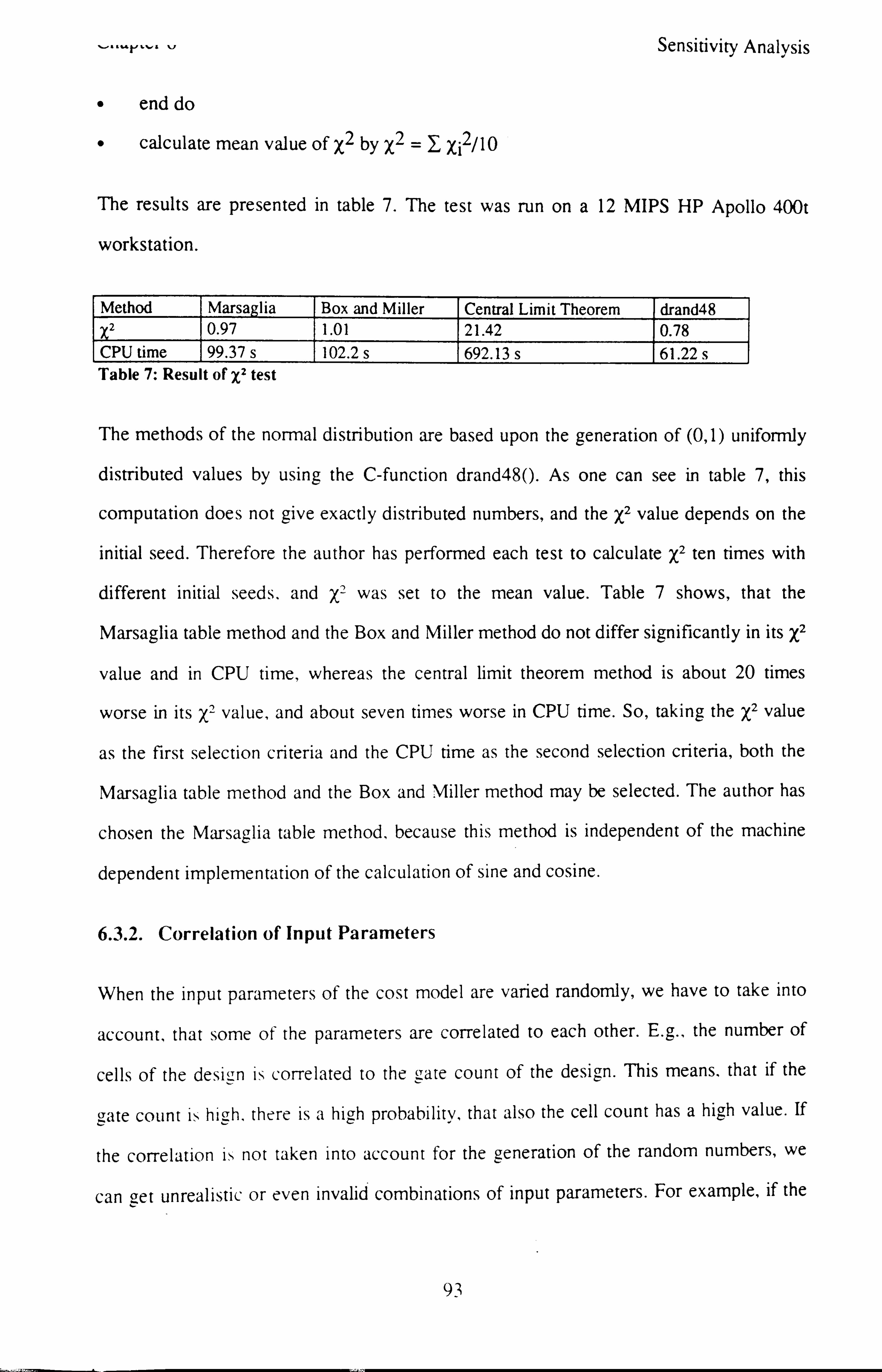
\ &lKr lVl J
0 end do
0 calculate mean value of X2 by X2 = Xi2ý10
Sensitivity Analysis
The results are presented in table 7. The test was run on a 12 MIPS HP Apollo 400t
workstation.
Method Marsaglia Box and Miller Central Limit Theorem drand48 0.97 1.01 21.42 0.78
CPU time 99.37s 102.2s 692.13s 61.22s Table 7: Result of XI test
The methods of the normal distribution are based upon the generation of (0,1) uniformly
distributed values by using the C-function drand48(). As one can see in table 7, this
computation does not give exactly distributed numbers, and the x2 value depends on the
initial seed. Therefore the author has performed each test to calculate X2 ten times with
different initial seeds, and x2 was set to the mean value. Table 7 shows, that the
Marsaglia table method and the Box and Miller method do not differ significantly in its X2
value and in CPU time, whereas the central limit theorem method is about 20 times
worse in its x2 value, and about seven times worse in CPU time. So, taking the x2 value
as the first selection criteria and the CPU time as the second selection criteria, both the
Marsaglia table method and the Box and Miller method may be selected. The author has
chosen the Marsaglia table method, because this method is independent of the machine
dependent implementation of the calculation of sine and cosine.
6.3.2. Correlation of Input Parameters
When the input parameters of the cost model are varied randomly, we have to take into
account, that some of the parameters are correlated to each other. E. g., the number of
cells of the design is correlated to the gate count of the design. This means. that if the
gate count is high, there is a high probability, that also the cell count has a high value. If
the correlation is not taken into account for the generation of the random numbers, we
can get unrealistic or even invalid combinations of input parameters. For example, if the
93

unapter d Sensitivity Analysis
gate count is uniformly distributed between 1000 and 10000, and the cell count is
uniformly distributed between 300 and 3000, there is a probability of 0.22, that the cell
count will be higher than the gate count, if these two values are independent. As we know, this cannot happen in reality, because in cell based designs a cell contains at least
one gate equivalent. In order to get realistic results for the Monte Carlo simulation, we
must take into account the correlation of parameters for the computation of the random
numbers. If we see the input parameters as a vector x, we can generate a random number
vector as follows:
x=C'"x0+µ (10)
where C* is given by
C` . C*T =C (11)
where C represents the covariance matrix. A proof is given in [Arm821. Because C is a
positive definite matrix, C* can be derived by using the Cholesky decomposition method
(see [Arm82]).
This method is used to calculate correlated multi variates, and it allows a correlation
between all variates. The correlation is defined by the covariance matrix. In the case of
the cost model, we have the following correlations:
crate count <=> cell count
gate count <=> number of flip flops
number of flip flops <=> sequential depth
This leads to the following covariance matrix for these three parameters:
gates: µ� 21
ý'31 0
cells: 2 µ22 0 0
flip flops: 4113 0 PL33 L-43
sequential depth: 0 0 µ34 µ44
where p ii is the -variance 6i2 of the single parameter i, and p ij is the covariance of
parameter i and parameter J. This is a special case of the covariance matrix, where the
parameters are correlated in pairs. In this case the method can be simplified as follows:
94

%-II"FL%-i U Sensitivity Analysis
X Gatt =P Gate +A
OGate 6Gatt
'ICell + (A VOGate V 7-
(12, ell F'' * Nell + AOCell p Cell )' ßCe1l XC
_ 13,14,15) V
7-ell XFIipFIop - F1ipFlop
+ (X W' PFlipFlop +n
OF1ipFlop FlipFlop )' ßFlipFlop
X SegDepth = t'SegDepth
+ (XOFlipFlop ' PSegDepth +X
OSegDepth ' V1
- PZStgDtptlt )' ßSegDtpth
This can be proven by using (10) and (11) for each pair of the correlated parameters.
In order to be able to generate the correlated random numbers, we must know the
distribution functions X* per parameter, the mean value p per parameter, the root to the
variance ß per parameter, and the correlation factor p per correlation. X*, p and ß are
variables. The correlation factor was derived by the author using data about existing
designs. The calculation of the correlation factors is described in appendix A.
6.4. General Sensitivity Analysis
A general study of the cost model is performed by the author in order to classify all
parameters of the cost model concerning their sensitivity impact on the total cost value.
This analysis is a special case of type 4 described in section 6.2., and it gives a general
idea, which parameters must be estimated very accurately, even if the cost for this
estimation is high, and for which parameters a rough estimate may fulfil the accuracy
requirements concerning the resulting cost value. An outcome of this study may even be,
that some of the parameters can be neglected for the cost evaluation. This fact would
allow a simplification of the cost model by cutting out the effect of these parameters. The
refined cost model would provide the same results with lower costs in data acquisition
and test strategy planning. Data acquisition costs are reduced, because the number of
parameters, for which data need to be provided, is reduced. Due to the reduced
complexity of the refined cost model, calculation effort in terms of CPU time and
therefore the related test strategy planning costs are reduced. A second point of cost
reduction concerning test strategy planning efforts is the fact, that a reduced number of
parameters and variables may lead to a reduction in the search space. If, for example,
two test methods differ only in parameters, which are no more- present in the refined cost
model, then these two test methods are identical concerning their impact on the test
95

unapter b Sensitivity Analysis
strategy planning process, which reduces the size in one dimension of the search space -
the test method alternatives - by one element.
The sensitivity classification of the parameters will be performed by estimating the
following characteristics of each parameter:
1. The mean value and the variance of the sensitivity of each parameter in a
constrained space DER of the input parameters:
fC'(x). f(x)dx -ý° (16,17)
62 =j (C' (X)_ µ)Z "f (x)dx
where p is the mean, 62 is the variance, C'(x) is the sensitivity of the total cost,
and f(x) is the probability density function of the input parameters of the cost
model.
2. The maximum sensitivity of the total cost for each parameter in a constrained
space DER of the input parameters:
Smax = nnax(C' (x))VX E De- R)
where x is the vector of the input parameters, and C'(x) is the sensitivity of the
cost model.
In this thesis all three characteristics will be estimated by performing a Monte Carlo
simulation. Due to the fact, that parts of the cost model are test method dependent, i. e.
the cost model is different for different test strategies, the sensitivity analysis was
performed for three different representative test strategies. These are no DFT. scan path
and circular self test path.
6.4.1. Estimation of Mean Value and Variance of Sensitivity
6.4.1.1. The Algorithm
The integrals to calculate the mean value and the variance will be estimated by a Monte
96
ý__ý_

-----r --- --
Carlo simulation as follows:
in -IC'(X, )
(18), (19)
CY = _. y
n-1 1_,
Sensitivity Analysis
where p is the mean value, 62 is the variance, C'(x) is the sensitivity, n is the number of
simulations and xi is the vector of random numbers for the input parameters of the cost
model. The random numbers per parameter are uniformly distributed. The range of the
distribution covers all typical values. They are defined in table 8.
Parameter Name Abbreviation Lower Limit Upper Limit Number of cells cells 3 64000 Complexity exponent cexp 0.8 1.0 Number of gates c gate 1,000 100,000 Labour cost rate costrate 500 S 5000 S Performance complexity cperf 1 3 CPU time cputime 0 1,000 h Design centre cost rate descentrate 10,000 S 40,000 S Computer equipment rate equrate 25 S 1000 S Designer's experience ex er 0 100 Required fault coverage fcreq 70% 100% Average number of faults per gate g 2 5 Constant factor concerning designer's productivity
Wes 1
Constant factor concerning total productivity
kp 70,000,0(X) 90,000,000
Manual test generation time per fault
mtgtime 0.05 h Ih
Number of flip flops dffs 6 8,00() Design originality or 0 1 Productivity of the CAD system pcad 1 5
Percentage of design time an external design centre is used
percuse 0% 100%
Number test pattern for which test application cost increases
pms 64,000 640,000
Test alication cost per step s 0 25 S
Production unit cost per gate puc 0.5 S 2S Sequential depth se de th 0 103 Production volume vol 1,000 1,000,00O
Table 8: Distribution characteristics of cost model parameters
The sensitivity S . (x º must be calculated for each input parameter. The sensitivity value is
defined here as the relative difference in the total cost of a relative difference of the
9 --

Lnapter b
analysed input parameter:
C, "s)-C(xi) Si _ (20) C (x; )
Sensitivity Analysis
where s is the sensitivity factor, which defines the increase of the parameter xi as a
percentage of xj. The author has chosen this definition of sensitivity instead of the
gradient dC/dxj, because the gradient does not allow direct comparison between different
parameters, because they are based on different measure units, and consequently the
gradients are not comparable. For example, a gradient of I for the parameter
"originality" is less sensitive than a gradient of 1 for the gate count. In both cases the
meaning of a gradient of one is, that a variation of the parameter value by one unit will
vary the resulting cost by one unit. This means, that a variation of the originality from 0.0
to 1.0 will have the same impact on the total cost as a variation of the gate count from
10,000 to 10,001 gates, if the gradient is constant for both parameters within the varied
range. The relative difference of the parameter as defined here is much better linked to
the original question of a sensitivity analysis, which is "how much does the variation of a
certain parameter impact the total cost? ". The sensitivity factor s will be set to 1.01,1.1
and 1.2, which means a variation of the parameter by I%, 10% and 20%. This allows to
analyse the sensitivity for small, medium and large variations. For some parameters,
especially those going into step like functions, e. g. the parameter "pin memory size", a
larger variation may cause a significant increase in the sensitivity, where a smaller
variation will lead to no sensitivity at all. The following example should illustrate this:
The test application costs are calculated by a step like function (see chapter 4). If the
number of test patterns is 1000 and the value of the pin memory size is uniformly
distributed between 500 and 1500, the. probability, that a I% increase of the pin memory
size will lead to an increase in the test application costs is
(1000- 1000) 1.01
=0.0099 (21) 1500 - 500
98

Lnapter 6 Sensitivity Analysis
If the increase of the pin memory size is 10%, the probability of a cost increase is
000) (1000-1 p 0.0909 (22)
5001500-
In the case of aI% variation, a Monte Carlo simulation will result in test application
increase in average every 100 simulations. For a 10% variation, this increase will be in
average for every 11 simulations. Therefore a1% variation will need more simulations as
the 10% variation to achieve the same accuracy.
6.4.1.2. Estimation Error of the Monte Carlo Simulation
Monte Carlo simulations are estimates which converge to the exact value of the integral.
The number of simulations needed to achieve a satisfying accuracy of the Monte Carlo
estimate can be derived from the standard error. The standard error is defined to
6S = 6-
(23)
where ßs is the standard error. If the variance converges to a certain value, the standard
error will converge to zero. Figures 16 through 18 show the standard error as a function
of the number of simulations for all parameters. The value printed is normalised to the
root of the variance, 6, for 10,000 simulations. The simulation was performed with a
sensitivity factor of 1.01 and "no DFT" as test method except for the parameter dffs,
were the test method "scan path" was chosen. This exception was made, because the
number of flip flops (dffs) does not affect the total cost for the "no DFT" test strategy.
99

Chapter 6 Sensitivity Analysis
80.00%
70.00%
60.00%
50.00%
40.00% 11
30.00% ' ý1
ý\
20.00% '
10.00%
0.00%
^, X_ýXXv ? ý'
_ NNNNNNNNNN
NMR V) ýG lý OC ý
cells
--- cexp
----- cgate
-- costrate
--- cputime
descentrate
--- equrate
exper
Figure 16: Standard error of Monte Carlo simulation for group 1
90.00%
80.00%
70.00% kdes fcreq
--- fPg 60.00%
- kdes 50.00%
--- kp 40.00%
---- mtgtime 30.00%
dffs
20.00% - All or
10.00%
0.00%
ry c^ý r1 NNNNNNN
rv r: ýc tý xa
Figure 17: Standard error of Monte Carlo simulation for group 2
100

unapter 6 Sensitivity Analysis
70.00%
60.00%
pcad
50.0090 '' -- percuse
40.00% ----- prns
PPS 30.00ßb
--
Ti.
mac
20.00% segdepth
--- Vol 10.0090
0.00%
NNNNNNNNN MTv: C [ý X
Figure 18: Standard error of Monte Carlo simulation for group 3
The figures show for all parameters except one good convergence to zero for the
standard error. The value remains under 10% for 3,200 simulations. The exception is
kdes. This parameter will need special attendance concerning its accuracy. However, for
most parameters the standard error remains at a significant level even with 10,000
simulations. This means, that the Monte Carlo estimate of the mean value and the
variance has some inaccuracy. Therefore a calculation of the confidence interval of each
estimate will be performed. The confidence interval [Kre75] defines a range, in which the
real value will be with a certain probability. This probability is called the confidence
coefficient. The confidence interval can be calculated for the mean value, if the sample
size, the variance of the sample and the confidence coefficient is given. The author has
selected a confidence coefficient of 0.998, which means, that the probability, that the
mean value will be in the confidence interval, is 99.8%. In figures 20 through 25 the
confidence intervals of the mean values of the sensitivity are printed. 10,000 simulations
were performed. In these graphs, the white square marks the upper bound and the black
square marks the lower bound. These show. that the average confidence interval remains
very small for 10.000 simulations in all situations. For most parameters the lower and
upper bound are so closed, that the lower bound (black square) is covered by the upper
bound. Therefore the author has selected 10,000 simulations as sufficient for this
101

,.....,. r...... ý,
I
Sensitivity Analysis
anaivsis.
1.60%
1.40%
1.20%
1.00%
0.80% 0
0.60% 0
0.40%
0.20% - 00
0.00% 171 0 0 NVL 'r ÜC j1
ý' J G. C. -, C. ° U 'J C4 -0 :J0v: vi y
>° EEt ' O' y
E - Q. j .5 zo
r J r
o 0' V E . J 7
Figure 19: Mean sensitivity for a1% variation and no DFT
35.00%
30.00%
25.00%
20.00%
15.00%
10.00%
5.00% .W G 7-
EI EI 0.00% ý7
J .)3G C
Figure 20: Mean sensitivity for a 20% variation and no DFT
102

Chapter 6 Sensitivity Analysis
1.20010
1.00% a
0 0 0.80%o
0.60%
0.40% '
0.20%
13 Q EI Ei Ei o Q o Qv 0.00q0 nU ,nm'aa U U mU U v, vN 'ý .TU
UG) 7 y UUu U U
Ü 4
Ü E
U
Figure 21: Mean sensitivity for a I% variation and scan path
25.00%
0 20.00%
O 0
15.00%
10.00%
5.00%
Q QQQ Q Qa Q a QQ 0.00% J 'r. - 'J GG
G
J J uu uA vJ - Q' J
C .U :J U G. 7 . sp r_ V r_
Figure 22: Mean sensitivity for a 20% variation and scan path
103

--nal. )LI-, l U Sensitivity Analysis
1.20%
1.00%
Q Q
0.80%
0.60%
0.40%
0.20%
OOO O O 0.009'0
UA VJ b. «i d
`-.. uM _-g X aY tJ quuö
m ý, > u
H u
E hNVC V"
aÄ`0cE ä x
U UJ ý U C U
Figure 23: Mean sensitivity for a I% variation and self test
25.00%
p 20.00%
0 p
15.00%
10.00% U
5.00%
EI EJ 0 EI ,
p ED 13
0.00%
C: G>7 E E
C JG JJ G jt GJ
Ü S "' J G
G E
Figure 24: Mean sensitivity for a 20% variation and self test
6.4.1.3. Results
In figures 25 through 35 for each parameter the range is printed, in which the sensitivity
will be in 99% of all cases. This range is defined as follows:
probability (sensitivity < lower bound) = 0.005
probability (sensitivity > upper bound) = 0.995
The range is marked by the vertical line and the mean value of the sensitivity is marked
104
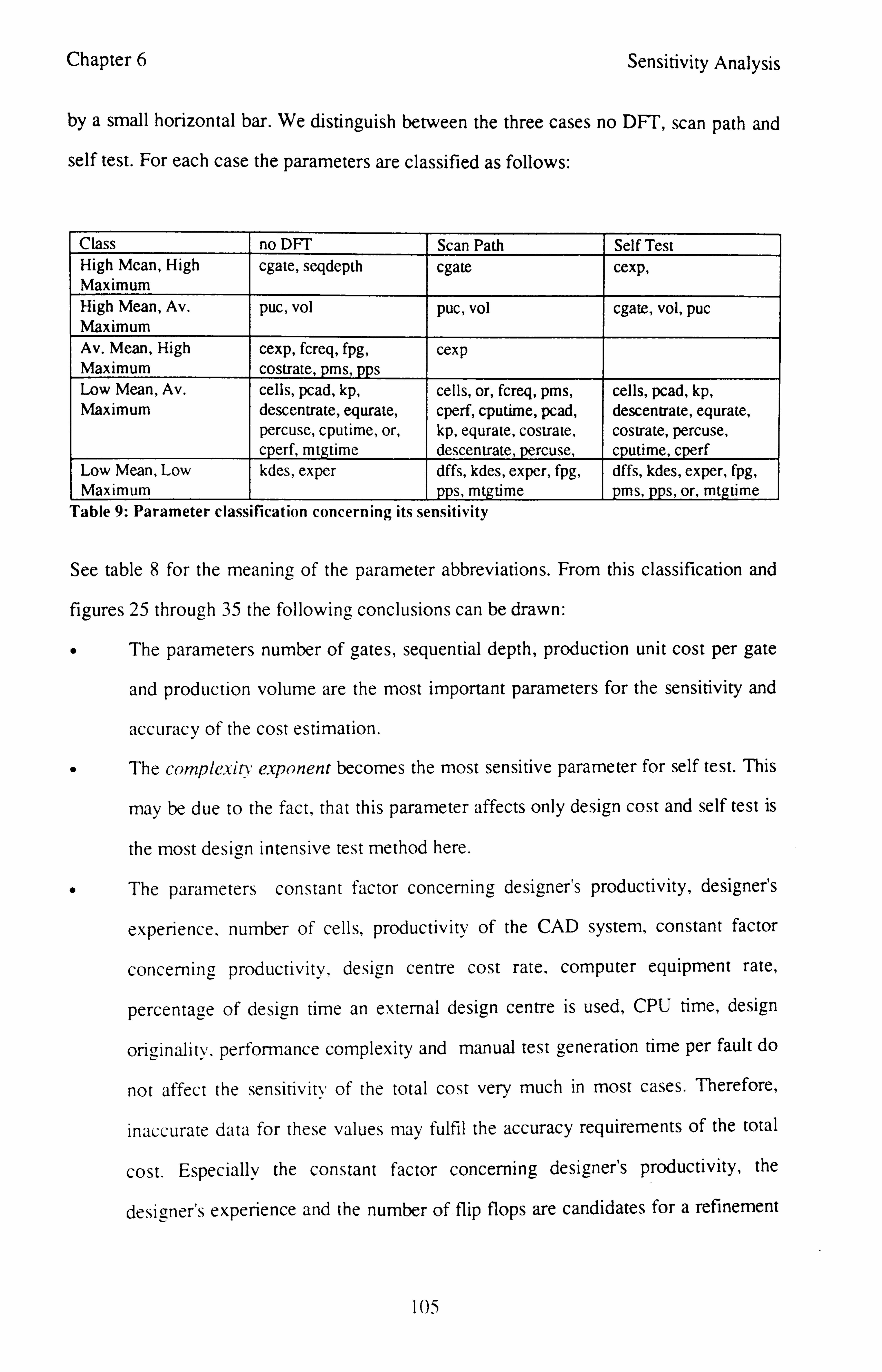
Chapter 6 Sensitivity Analysis
by a small horizontal bar. We distinguish between the three cases no DFT, scan path and
self test. For each case the parameters are classified as follows:
Class no DFT Scan Path Self Test High Mean, High cgate, seqdepth cgate cexp, Maximum High Mean, Av. puc, vol puc, vol cgate, vol, puc Maximum Av. Mean, High cexp, fcreq, fpg, cexp Maximum costrate, ms, s Low Mean, Av. cells, pcad, kp, cells, or, fcreq, pms, cells, pcad, kp, Maximum descentrate, equrate, cperf, cputime, pcad, descentrate, equrate,
percuse, cputime, or, kp, equrate, costrate, costrate, percuse, cperf, mtgtime descentrate, percuse, cputime, cperf
Low Mean, Low kdes, exper dffs, kdes, exper, fpg, dffs, kdes, exper, fpg, Maximum s, mtgtime ms, s, or, mt time
Table 9: Parameter classification concerning its sensitivity
See table 8 for the meaning of the parameter abbreviations. From this classification and
figures 25 through 35 the following conclusions can be drawn:
" The parameters number of gates, sequential depth, production unit cost per gate
and production volume are the most important parameters for the sensitivity and
accuracy of the cost estimation.
0 The com plexioy exponent becomes the most sensitive parameter for self test. This
may be due to the fact, that this parameter affects only design cost and self test is
the most design intensive test method here.
0 The parameters constant factor concerning designer's productivity, designer's
experience, number of cells, productivity of the CAD system, constant factor
concerning productivity, design centre cost rate, computer equipment rate,
percentage of design time an external design centre is used, CPU time, design
originality, performance complexity and manual test generation time per fault do
not affect the sensitivity of the total cost very much in most cases. Therefore,
inaccurate data for these values may fulfil the accuracy requirements of the total
cost. Especially the constant factor concerning designer's productivity, the
designer's experience and the number of-flip flops are candidates for a refinement
105

------r --- -- Sensitivity Analysis
of the cost model, which will not use these parameters or will take an average
value for them.
0 Only one of those parameters, which purely affect the design cost, is important.
This is the complexity exponent. This fact arises the question, whether the Monte
Carlo simulation is dominated by the production volume dependent cost. The
author has therefore performed a Monte Carlo simulation, where the production
volume was varied between 1,000 and 2,000 (Low Volume). The results are
presented in figures 34 through 35. They show, that the classification of the
parameters is still the same, whereby the difference of the mean sensitivity
between the parameters is smaller. The main difference between this case and a
production volume varied over the full range is a larger variance and a higher
maximum value for the parameter complexity exponent. This shows, that the
assumption, which was made, does not follow.
The next question to answer now is, whether some of the "insensitive" parameters can be
neglected such that the cost model can be refined. This question can be answered by
determining the maximum sensitivity as a worst case. This analysis will be performed in
the next section.
30.00%
25.00%
20.00%
15.00% T I.
10.00%
5.00%
0.000/0 C-, __ V) s, _0 Cl. n 11) 11) v vi -5 a" u. cv --` öQv LI CL aa ýI yzEä Cl- va 'D E
Tv Lt L) _QI Cr jtr ro a
ID La L)
ý7
Figure 25: 99% range of sensitivity with a I% variation, no DFT
106

C. napter b Sensitivity Analysis
30.00%
25.00%
20.00%
15.00%
10.00%
5.00%
0.00% 'ý USy -0 dd 4J 0) Qý p al U to v> y "ý ". Q dl
CL x ü _ID Xe io a>
.Eä ä°° E
ýý Ud cr
y Uý CI UU
UÜUüäÜ Vi y
Figure 26: 99% range of sensitivity with a 10% variation, no DFT
80.00%
70.00%
60.00%
50.00%
40.00%
30.00%
20.00%
10.00% :4L 0.00%
L) -v a in. v a) 2 CA a) a) NN 't-- CT au
,n -` ä) LL L) U3aÜa Qä
LU 'l) Q
CC) äa
NN
Figure 27: 99% range of sensitivity with a 20% variation, no DFT
107

Chapter 6 Sensitivity Analysis
6.00%
5.00%
4.00%
3.00%
2.00%
1.00%
0.00° =U" V) v Cl Cl Q) (L) Q) OI Qi cu "H () -- 6Qv CL CL > Cl -; 6 4u 10 -2 E
,ýn Cl. a
(L) cr 0 (u (I UUQ. UE 0
Figure 28: 99% range of sensitivity with a I% variation, scan path
70.00%
60.00%
50.00%
40.00%
30.00%
20.00%
10.00%
0.00% L2 Z+ Cl. a aI a) Q1 al a. ) (U 'H
43 vä-v ýv ýo ýv a>-EEä ;oä°2E a ' a, Cl. U
d) Cr z L) Ü Cl. ä
of ° U <n 9)
Figure 29: 99% range of sensitivity with a 10% variation, scan path
108

Chapter 6 Sensitivity Analysis
90. OOýk
80.006
70.00%
60.00% 50.00%
40.00% 30.00% 20.00%
10.00%
0.006 N C} NN ru -0 Q. N (1) Q) QI Q) 0NN Q1 "Q Q1
V cl _0 NaVjZVzaL Cl. -NC VV _vQ 00naE
Q)
Figure 30: 99% range of sensitivity with a 20% variation, scan path
8.00°
7.00%
6.00%
5.00%
4.00%
3.00°6
2.00%
1.00%
0.00° Qj `O Qy V. ý Li T) CL a a1 aY dl QI al Ql Vi Vl Q
Ü Z' a `ä üJNü5aa 01 Q. V
Üä Cl. E 2ý
Figure 31: 99% range of sensitivity with a I% variation, self test
109

'T ?T
LIIgpLG1 V Sensitivity Analysis
J. 0O%
80.00%
70.00%
60.00% 50.00%
40.0 %o
30.0 %o
2 0.0 0%
10.00%
0.00% --ý j-i-i --i -i w
IV (2. c2. w cu Q) Ch - ;v ;o "v a3.
EEe Zv -Ei -13 ° rj>r E ä
axi a Z, v, vn Cl °'
ä '. = zj Z !5 :3Q Q ä0
to V
Figure 32: 99% range of sensitivity with a 10% variation, self test
160.00%
140.00%
120.00%
100.00%
80.00%
60.00%
40.00%
20.00%
0.00%
Figure 33: 99% range of sensitivity with a 20% variation, self test
w ýý w T, aav t) Q) CM o0 1) ti Q) öQ aý 1 aý ä It, -. )4 " 16 7o > 01 EEa Cl. a z' ä (-) zypa Q' v rn
L) CU Q°äa
U 4?

°ö ö c'
Chapter 6 Sensitivity Analysis
7.00%
6.00%
5.00%
4.00%
3.00%
2.00%
1.00%
0.00° -0 ci. CL a) 0) (D c31 -(D 0 4) cr
v Cl. Ve :3HüZ MVb LÜ0äaE
Vi y a)
Figure 34: 99% range of sensitivity with a 1% variation, no DFT, low production volume
160.00%
140.00%
120.00%
100.00%
80.00%
60.00%
40.00%
20.00%
0.000/0 L
U -0 aa U) a) a) aI ý U) a) HN a- äQ aý a, ä CL °T5 iv -> E 3. ää UnY (U Ca. U=: VCU
06a 1U (U UaUE nH
Figure 35: 99% range of sensitivity with a 20% variation, no DFT, low production volume
6.4.2. Estimation of the Maximum Sensitivity
As already mentioned in the previous section, the sensitivity to the total cost for some
parameters remains negligible in at least 99% of all cases. This leads to the question,

Chapter 6 Sensitivity Analysis
whether the total cost is insensitive to these parameters at all. To answer this question,
the maximum sensitivity for the parameters must be determined. If the maximum
sensitivity is negligible, the cost model can be refined by taking out the insensitive
parameters. The gains of this refinement have been discussed in the introduction of
section 6.2..
In this section, the author will describe the methods he has developed in order to
determine the maximum sensitivity and he will present and discuss the results.
6.4.2.1. The Algorithm
The author will now introduce the definition of the maximum sensitivity as it is used in
this thesis. Therefore the following definition will be made:
40 The total cost difference for parameter i is defined to
CD, (x) = C(x, x, o) - C(x, x,, ) with C(x, xto) >_ C(x, xj, ) (24)
0 The relative difference for parameter i is defined to
RDi(x) - C(x, x1)-C(x, xLl) (25)
C(x, xLO)
0 The maximum total cost difference for parameter i is defined to
CDmax, (x, xi) = max(CD, (x, x, ))d(x; o, x� EDE R) (26)
where D is the constrained search space of xi as defined in table 10. This means,
that CDmax is such that, if all parameter values beside xi are kept constant, xip is
the maximum and xil is the minimum of the function CDi(x, xi).
0 The relative maximum difference for parameter i RDmax is defined to the
relative difference of the maximum total cost difference.
40 The maximum sensitivity for parameter i is defined to
Smati (x) = max(RDmaY (x))V(x # Xi EDE R) (27)
This means, that the maximum sensitivity is determined by that combination of
input parameters which leads to the relative maximum difference in the total cost
112

Chapter 6 Sensitivity Analysis
which can be caused by the variation of parameter i.
The author will use this definition of the maximum sensitivity for deciding, whether a
parameter can be taken out of the cost model.
In order to determine the maximum sensitivity, we need to determine the relative
maximum difference. If the function CD(xi) is monotone, the maximum and the minimum
of CD is given by the upper and the lower limit of the constrained space of the
parameter. Because this is not always the case, the author has selected the following
approximation method to determine the maximum and minimum of CD:
113

Chapter 6 Sensitivity Analysis
calculate_CDmax() xmin is the lower bound of range xmax is the upper bound of range minind = maxind =1 while ((recursion depth less than 5) and (minind and maxind are not 0 or 10))
Cmin =0 Cmax = maximum float number minind =0 maxind = 10 for i from 0 to 10
Cx = C(xmin + i"(xmax-xmin)/10 if (Cx > Cmax)
Cmax = Cx maxind =i
else if (Cx < Cmin) then Cmin = Cx
minind =i endif
endfor if (minind and maxind are not 0 or 10) then
xmin = xmin + max (0, min (minind, maxind)-1)"(xmax-xmin)/10 xmax = xmin + min (10, max (minind, maxind)+l)"(xmax-xmin)/10 increment recursion depth
endif endwhile RDmax = (Cm,, -Cmin)/Cmnx
This algorithm will give a good approximation of the relative maximum difference, if the
sensitivity of the function does not vary too much, i. e. there are no "sharp peaks" in the
function. This can assumption can be made for the cost model.
The maximum sensitivity can be determined by a Monte Carlo simulation as follows:
U" T1 ( (28) max
= max( 1_1
CDmax (xi)
The values of x are sampled from uniformly distributed variates as defined in table 8.
This method requires a large amount of simulations to achieve sufficient results, because
we want to determine a specific element out of an infinite set of parameter combinations.
The following example should illustrate this:
The number of parameters is 23. If we divide each parameter range into four sub
ranges, and if we want to combine all sub ranges for all parameters, the number
of combinations is 423. There is no chance to run so many simulations.
114

Chapter 6 Sensitivity Analysis
Therefore the author has developed a technique to reduce the sample by keeping the
accuracy of the result. This technique will be described in the following section.
6.4.2.2. Reduction of the Sample Size
There are several publications which are related to Monte Carlo optimisation ([Ant82],
[Kje81], [Rub86]). All of them address the problem of reducing the sample size by using
a technique called importance sampling. This technique exploits the random samples of
the past for generating the random samples in the future. In [Ant82] and [Kje8 l] the
importance sampling techniques closely linked to the problem to solve, which is different
from the problem to be solved here. In [Rub86], the techniques presented are more
general. The author has therefore implemented a different algorithm. In this algorithm the
Monte Carlo simulation is divided into two phases:
1. In the first phase Monte Carlo simulation is performed with the input parameters
uniformly distributed. In this phase we make an estimate of the values of the input
parameters, which will lead to a high sensitivity. We call these values maximum
sensitivity, values.
2. In the second phase Monte Carlo simulation is performed with a distribution
function for the input parameters, which is adopted to the maximum sensitivity
values. In this phase the sensitivity values are updated with each simulation. This
means, that in this second phase the parameter values are sampled in the region
where we expect the actual maximum sensitivity value.
The algorithm is implemented as follows:
calculate max_sens( for L times
perform Monte Carlo simulation with uniformly distributed variates as input parameters and determine RDmax
endfor select M samples from all previous simulations which cause the M maximum RDmax for N times
perform Monte Carlo simulation with importance samples and determine RDmax" update the Ni maximum samples with the sample which just was calculated.
I15

Chapter 6 Sensitivity Analysis
I endfor
The importance samples are based upon the input parameter values of the M maximum
les, and they are calculated as follows: importance_sam pling()
determine the distribution of the parameter values which are related to the M maximum samples. constrain this distribution by the lower and the upper limit of the parameter range generate a variate from this distribution.
The generation of a variate based on the determined distribution function was
implemented by applying a table method which is similar to the Marsaglia table method.
Instead of using the table for a normal distribution, we take the table of the values for the
M maximum samples.
The object in this method is to concentrate the distribution of the sample points in the
parts of the parameter range that are of most importance instead of spreading them out
evenly. Nevertheless, the L simulations with a uniform distribution function are needed
to make a good estimate about which parts are important. If a certain parameter has
influence on the maximum sensitivity, the related importance sampling distribution will
converge to a certain value, which we expect to be the value for the maximum
sensitivity. The speed of the convergence and therefore the sample size and the risk of
running into a local maximum is driven by the values L and M. A high value for M will
cause slow convergence but a low risk of running into a local maximum and vice versa.
A higher value for M will lower the risk of running into a local maximum but will
increase the sample size and therefore computer runtimes. The author has performed
some experiments with different values for L and M to find a good trade-off. In the next
section, the values for L, M and N will be presented and the maximum sensitivity values
for the parameters which are expected to be insensitive will be presented and discussed.
6.4.2.3. Results
The author has found 'N'1=10 and L=300 to be a good trade-off between fast convergence
and a low risk of running into a local maximum. The total number of simulations L+N
116

"I ij rlr rj L,
I jri iI F. I iiH
Chapter 6
was set to 1000.
Sensitivity Analysis
The maximum sensitivity was determined for the following parameters:
performance complexity, design centre cost rate, designer's experience, average
number of faults per gate, constant factor concerning designer's productivity,
constant factor concerning total productivity, manual test generation time per
fault, number of flip flops, productivity of the CAD system, percentage of design
time an external design centre is used.
The analysis was made for the test strategies no DFT, scan path and self test. The
resulting maximum sensitivity in percentage of the related maximum cost is shown in
figure 36. This graph shows, that the maximum sensitivity exceeds 20% for 0
parameters, which is by far too high to neglect. This means, that for all parameters
situations may occur, where a variation of the parameter within the range defined in table
8 can lead to more than a 20% variation of the total cost. A simplification of the cost
model in general by removing parameters is therefore not possible.
100%
90% 80% 70% no DFT 60% 50% [1 Scan Path
40% 30% Self Test
20%
10% 0%
` r
Figure 36: Maximum sensitivity values
6.5. Iterative Sensitivity Analysis
The second application of sensitivity analysis studied in this chapter is identical to type 4
mentioned in section 6.2.. This application leads to a test strategy planning procedure in
iterative steps as follows:
117

Chapter 6 Sensitivity Analysis
1. Make a rough and inexpensive estimate of the input data.
2. Perform test strategy planning.
3. Perform a sensitivity analysis in order to find out, which parameters need to be
defined more accurately. These are those parameters, which have a high
sensitivity.
4. If accuracy of the result is OK, then the test strategy planning procedure is
finished, else make more accurate estimates for the most sensitive parameters and
go to step 2.
In the iterative sensitivity analysis, the same methods are used as for the general
sensitivity analysis. The main differences are the iterative procedure and the different
distribution of the parameter values. For the general sensitivity analysis, we used a
uniform distribution for all parameters in the range of all possible values. For the iterative
sensitivity analysis, we have inaccurate estimates for the parameters, which can be either
a uniform distribution or a normal distribution.
6.6. Total Variation Sensitivity Analysis
The third application considers the fact that there is a certain cost limit for data
acquisition, which makes estimated input data remain inaccurate. This means that the
decision criteria, i. e. the resulting cost value, is subject to inaccuracy. This inaccuracy is
different from test strategy to test strategy. The following example will illustrate this fact.
Comparing the test method "scan path" in combination with combinational ATPG to "no
scan path" in combination with sequential ATPG, the related test generation cost as part
of the resulting cost are much more uncertain for "no scan path". The reason for that is
the inaccurate parameter "sequential complexity", which affects sequential ATPG cost
but not combinational ATPG cost. This fact may lead to a situation, where the resulting
costs for the sequential ATPG approach are lower as those for the combinational ATPG
assuming that the estimated value for the sequential complexity is exact, but that there is
a high probability, that the costs will be much higher for the sequential ATPG approach,
118

Chapter 6 Sensitivity Analysis
considering the high probability that the sequential complexity will be higher than
estimated.
In order to take the inaccuracy of the cost estimation into account, the author will
replace the total cost value by the distribution function of the total cost value as the
optimisation criteria.
6.6.1. The Algorithm
The distribution function F(x) will be used to determine with a given cost probability pc
the upper cost limit CL:
CL =F-'(p, ) (29)
The cost probability has to be defined by the user of the test strategy planner. This cost
probability is defined as the probability, that the total costs will be less than the related
cost limit, due to inaccuracy of the input data. The value for the cost probability
represents the risk of the cost estimation and by that the risk of the decision. In other
words, the risk of the decision is the risk, that the chosen test strategy is not the
optimum. This type of sensitivity analysis application is an extension to type I in section
6.2.. There, the sensitivity analysis is applied to the "solved problem", which is the
selected test strategy alternative. Here, the sensitivity analysis is applied to the selection
procedure, which is the test strategy planning procedure.
The calculation of the cost limit is implemented by performing Monte Carlo simulation.
If the n cost values resulting from n simulations are stored in a sorted list c[n] in rising
order, the cost limit can be estimated by a linear approximation as follows:
CL=c[int(n. p, )]+(c[int(n-p, )+1] -c[int(n"p, )])"(n"pc-int(n-p, )) if p, <1
CL = c[int(n p 1] ifcp= 1
where int(npc) is the integer of the product npc. It represents the index in the list
of cost values, which points to the cost value which is closest to the estimated
119

Chapter 6 Sensitivity Analysis
cost limit.
6.6.2. Determination of the Number of Simulations Needed
The accuracy of the determination of the cost limit as described in the previous section
depends on the number of simulations for two reasons:
" The Monte Carlo simulation is an unbiased estimator for the distribution of the
total costs. This estimator is subject to inaccuracy as long as the number of
simulations is finite.
0 The linear approximation is subject to inaccuracy which depends on the curvature
of the distribution function in the region where the linear approximation is made,
and it depends on the number of simulations.
The author will therefore study the impact of the number of simulations on the accuracy
of the cost limit estimation in order to determine an appropriate number for the Monte
Carlo simulations.
The techniques used in 6.4.1 to determine the estimation error cannot be used here,
because they are related to the estimation of the mean value and the variance, where in
this analysis we estimate a certain value of the distribution function. The author has
decided study the convergence of the Monte Carlo simulation for analysing the
estimation error and the number of simulations needed to keep the error under a certain
limit. Due to being an unbiased estimator, we can assume, that the Monte Carlo
estimation will converge to exact value by increasing the number of simulations. If the
difference between succeeding estimations during the Monte Carlo simulation become
very small, we take the related value as the exact value. Based on this exact value CL the
relative estimation error for an estimate CLest is given by
CL - CLesý (30)
e'" CL
The author has performed the convergence study for the test strategies no DFT, scan
120

Chapter 6 Sensitivity Analysis
path and circular self test path, and for the following cost probabilities:
99%, 90%, 75%, 60% and 50%.
The relative estimation errors are shown in figures 37 through 39. The author has
selected the cost limit for 10,000 simulations as CL. The graphs show, that for cost
probabilities of 90% and 99% the estimation error converges slower to zero than for cost
probabilities of 50% or 60%. This is because of the larger gradient of the inverse
distribution function F-1(pc) for the high end and low end regions of the function, for
which an argument difference affects the related cost limit more than for lower gradients.
The relative error remains for all curves under 5% for simulation number greater than
200. The author proposes therefore a simulation number of 200 to perform Monte Carlo
simulations for total variation sensitivity analysis.
Some representative results will be presented and discussed in chapter 8.
40.00%
35.00%
30.00% 0
25.00%
20.00%
15.00%
10.00%
5.00%
0.000/0
#simulations
---------- 50%
ÜO%
75%
90%
99%
Figure 37: Convergence of Monte Carlo simulation for no DV I
121
TO Cý Cý QQOOOO Q Cý OO=O Gý O-O
ýý 1ý 4 LO (jo rý 00 so

Lnapter b
35.00%
30.00°6
ö 25.00%
20.00%
15.00°6
10.00%
5.00%
o. oo%
#s imulations
.................. 50%
" .................. ÜO%
75%
90%
................... 99%
Figure 38: Convergence of Monte Carlo simulation for scan path
35.00%
30.00%
25.00%
0 20.009/o - cu 15.00°
10.00%
5.00%
0.000/0
------------------ 50%
..... ......... ÖO%
75%
90%
................... 99%
Figure 39: Convergence of Monte Carlo simulation for self test
6.7. Summary
Sensitivity Analysis
In this chapter the author gave a literature survey on sensitivity analysis and presented
the techniques he has developed to perform sensitivity analysis for three different
applications:
0
I
the general sensitivity analysis was performed to classify the cost model
parameters concerning their sensitivity impact to the total costs.
the iterative sensitivity analysis is used to make iterative cost parameter
1? '
OOOOOOOOOO OOOOOQOOOO
tV MQL! ) C. t- co C) O V-
CD OOOOOOO C, OQOOOOOmO r- NM4 LC) C9 N- CC) 0. -
#s imulations

Chapter 6 Sensitivity Analysis
estimations, which can reduce the cost for gathering data for the parameters.
0 The total variation sensitivity analysis allows to perform test strategy planning
with uncertain or inaccurate cost model parameters, which are described by their
distribution. The optimisation criterion is based on the distribution of the total
cost instead of an average value. The user of the test strategy planning system can
select to take a basis for the system's decision for lower cost with a high risk to
be exceeded or for higher cost with a low risk to be exceeded.
All applications are based on Monte Carlo simulations. This technique was introduced
and adopted to the problems described in this chapter.
The general sensitivity analysis showed, that for each parameter configurations may
occur, which lead to a maximum sensitivity of more than 20% of the total cost. But in
most cases, the total cost is sensitive to only a few parameters of the cost model. These
are the number of gates, the sequential depth, the production unit cost per gate, the
production volume and the complexity exponent. Based on this outcome, the author
proposes to perform economics based test strategy planning as follows:
0 Provide values for the "important parameters" listed above.
0 Perform iterative sensitivity analysis until the accuracy requirements are fulfilled.
This method can drastically reduce the effort spended in data gathering, because in most
cases the accuracy requirements can be fulfilled by providing values only for a few
parameters.
The cost model which was studied in this chapter calculates the costs related to the
design and production of an ASIC. The methods were implemented for the test strategy
planner for ASICs. But many design-for-testability methods produce cost savings in cost
areas, which are not covered by the ASIC cost model, and which are related to the
design and production of boards and systems. The next chapter will describe a test
strategy planner which allows to plan and analyse the economics of test strategies for
boards and systems.
123

Chapter 7
Chapter 7
ECOvbs: A Test Strategy Planner...
ECOvbs: A Test Strategy Planner for VLSI based Systems
The EVEREST test strategy planner for VLSI based systems, here called ECOvbs, was
developed under the task "Test Economics Modelling" of the EEC funded ESPRIT
project "EVEREST" in collaboration of Brunel University and Siemens-Nixdorf-
Informationssysteme AG (SNI). The aim in this task was to develop and to evaluate test
economics models and to use them in a test strategy planning system, whose
development also was part of the project. Both the test economics modelling work and
the development of the test strategy planner was performed for the application to VLSI
test strategies and to VLSI based system test strategies. In chapter 5 the author
described the test strategy planner ECOTEST, which targets test strategy planning for
VLSIs. This chapter will present the test strategy planning system ECOvbs for VLSI
based systems.
The tools developed in the EVEREST project are intended to be used in industrial
environments by the partners of the project. This aspect, and the fact, that such a system
had never been developed before (the reasons are discussed in the next section), were the
basis of the following generic requirements for the system:
1. The system should take into account industrial practices and needs.
2. The system should therefore gain from the experience made in manual test
strategy planning by quality assurance people.
3. The system should be integrated into an industrial environment.
4. Due to being a novel approach and a research work, the system should be a good
compromise between the state-of-the-art in research and the applicability of the
system in industry.
ECOvbs was designed and developed by SNI and Brunel University in an
industrial/academic collaboration. Due to being employed by SNI, the author had good
access to industrial data. experience and user requirements of such a system. By working
124

Chapter 7 ECOvbs: A Test Strategy Planner...
in a research environment in collaboration with an academic organisation, the author was
able to design and develop a system, which fulfils the needs of industrial users, but
includes features and techniques, which are completely novel and ahead of state-of-the-
art. The specification of the work was based upon extensive talks to industrial users, a
detailed research in literature, and many fruitful discussions between the partners in the
task.
In this chapter, the author will first discuss the philosophy of the test strategy planner and
the arising needs of such a system in industry. In the subsequent sections, an overview of
the architecture of ECOvbs will be given, and its components will be described in detail.
7.1. Philosophy of ECOvbs
In the early 80's the manufacturing efficiency became the cornerstone in industry with the
main objective to build the highest quality product at the lowest possible cost(see
[Pyn86]). Pynn states, that "today's successful business requires an objective which takes
both product quality and manufacture efficiency into account" [Pyn86], and based on this
statement, he defines the following manufacturing objective:
To develop a production strategy which will achieve a product with superior
quality manufactured at the lowest possible cost.
One crucial part of the production strategy, especially in the field of VLSI based systems,
is the test strategy. The test strategy is the essential factor to quality. And it affects
nearly all cost areas of an electronic product.
Pynn [Pyn86] defines a test strategy as follows:
A successful test strategy is the optimum arrangement of various testers in
the circuit board manufacturing process that will result in products of
maximal quality at minimum cost.
Based on this definition, the technical factors affecting the test strategy are the fault
125

Chapter 7 ECOvbs: A Test Strategy Planner...
spectrum, the process yield, the production rate or volume and the product mix, i. e.
aggregation of active board types in a production line. The economical factors are the
tester acquisition cost, the tester adaptation cost (fixture cost and test generation cost)
and tester operation cost.
In this approach it is assumed, that for a given test strategy the technical factors are
fixed, and a test strategy is purely built upon a mixture of test applications. A similar
definition of test strategies is made in [Dav82]. This definition of a test strategy makes
the test strategy planning task relatively simple for the following reasons:
0 The only degree of freedom in the strategy planning is what test equipment
should be used in which phase of the production cycle.
0 Therefore the cost areas affected by a test strategy are only the cost related to the
test equipment, as defined in the previous paragraph.
9 Decisions about the test strategy can be made rather late. The first phase in the
product life, which is affected by the test strategy, is the test generation phase,
which in the past was done after the design cycle.
0 There was no large multitude of test equipment. Automatic test equipment arised
at the end of the 60's, and only a few companies shared the market on the test
equipment.
0 The rate of change in technology and therefore test technology was much lower
than today.
These factors were the main reasons, why there was no need for a test strategy planning
tool. The task of test strategy planning was confined to the selection of a new test
equipment or the proof, whether the existing tester scene is appropriate for the new
product.
Today the situation has completely changed:
0 People know that quality and production costs are mainly determined during the
specification and design phase of the product. Reinertsen claims, that "decisions
126
Chapter 7 ECOvbs: A Test Strategy Planner ...
on technology, architecture and physical structure, which typically occur during
the first few months of the design process, determine 90% of the product cost
and the majority of its capabilities" [Rei83]. A similar statement is made by
Szygenda: "... although the system design phase of product development
represents only about 15% of the product's cost, it has a 70% impact on that
product's operation and support cost" [Szy92].
0 Today, design methods are available to control the production and the quality.
Design for testability (DFT), design for manufacture (DFM) or concurrent
engineering are the keywords in this field.
0 Because of rapid technology changes, the product life time becomes shorter, and
this fact and an increasing competition in the market leads to enormous price
pressures in the electronics market. This arises the need for low production cost
right from the beginning of the production.
For these reasons, a today's test strategy includes, beside the usage of test equipment, the
design-for-test and design-for-manufacture methods, and therefore the author's definition
of a test strategy (section 3.2) is different from that used by Pynn.
A test procedure consists of the provision of the test equipment and the environment to
utilise it, the adaptation of the test equipment to the device under test, i. e. the hardware
adaptation and the test program generation, and the test application. The design methods
are those which facilitate the realisation of the test procedure (DFT) and those which
support the avoidance of errors. or, more specific, which increase the yield in the
production (DFM).
The optimum test strategy can be defined as follows:
An optimum test strategy is a test strategy. which meets all given product
constraints and the system's final quality requirements by minimum total
cost.
127

Chapter 7 ECOvbs: A Test Strategy Planner...
Based on this definition and the changing technology, design, production and market
around electronic systems, the determination of the optimum test strategy and therefore
the test strategy planning task is much more complicated than an approach based on a
test strategy as defined by Pynn [Pyn86]:
9 The test is now completely integrated into the design process. Therefore the
decision on the test strategy must be made very early in the specification phase of
the product. This makes the derivation of the test strategy factors, such as the
prediction of yield, fault coverage, production cost or test adaptation cost much
more complicated and uncertain. Especially in an environment with quickly
changing technologies, it becomes very difficult to make the estimation of the
factors, because we cannot gain from data of previous products.
" The estimation of the total cost is much more complicated as the estimation of
the economic factors as defined by Pynn, which are purely related to the test
procedure. Today's test strategies affect cost areas such as design cost for
different design alternatives, component procurement, cost of the production
process. test generation cost or test-, diagnosis- and repair cost in the production
or in the field. All these costs have to be determined in a product phase, where
factors such as the production yield, production volume, design complexity, fault
coverage of a test or the fault spectrum cannot be measured and therefore are
based on estimates.
" The multitude of test strategies is increased by another dimension, which is the
design option.
0 Factors such as the fault coverage per test and the production yield are
continuous parameters of the test strategy, which need to be optimised per test
strategy to analyse. This optimisation process (which is the optimum mix of yield
and fault coverage in order to achieve a given product quality? ) can be on its own
an extremely complicated task.
" The planning of test strategies will need organisational changes and changes in
responsibilities in most of the companies. because the implications of a test
128

Chapter 7 ECOvbs: A Test Strategy Planner...
strategy are no more limited to the production people (see also [Dav92]). The
implementation of a test strategy as defined here involves most parts of the
company: engineering, manufacture, finance, service, purchase and even
marketing and sales (e. g. to determine what quality level the market requires).
All these aspects necessitate a structured support for the test strategy planners. This
support can be given by a software tool, which supports the user in
" providing all factors which are needed to determine the optimum test strategy,
" evaluating the test strategies concerning its economics and compliance to quality
and design constraints,
0 optimising the parameters of a test strategy, and
" selecting the optimum test strategy.
The development of such a tool was the objective of the test economics task in the
EVEREST project. The author has designed and developed this tool in collaboration
with Brunel University. This tool, which is called ECOvbs, will be described in this
chapter.
A test strategy for VLSI based systems includes test procedures at all levels of
integration. Therefore the test of the components and the related test strategy is part of
the test strategy of the entire system. Also, for several DFT methods, which are
implemented at component level, or which are used for component level test, gains are
achieved for board level or system level test. In particular, boundary scan is implemented
in the component for supporting the board level test. Other examples are the scan path
technique, which was originally used and demanded by the system test people for
diagnostic purposes ([Sed92]), or built-in self test techniques, which are used for board
test and diagnostics. These aspects make the test strategy planning task hierarchical, and
the test strategy planning system for VLSIs, ECOTEST, can be integrated into ECOvbs
for the test strategy planning task at component level for the VLSIs.
Due to good progress which the author made with object-oriented programming in C++,
129

Chapter 7 ECOvbs: A Test Strategy Planner ...
ECOvbs was implemented in C++. This allowed the reuse of software components,
which the author had developed for ECOTEST, such as the cost model calculator or the
command handler. It is very easy to integrate C-components in C++, which was
important, because the experience in C is much more common than in C++, and which
allows to use code generators such as LEX or YACC. Another advantage of C++ as an
object oriented language is, that the performance of the executable program is much
better than implementations in other object-oriented languages, such as Smalltalk.
As this was a collaborative project, it is important to indicate the areas of the author's
contribution. The cost model evaluator and the interface to the cost model text files were
taken from the author's implementation of the C++ version of ECOTEST. The author
has added some calculation functions. The interface to the test method descriptions was
specified and implemented by the author as well as the test strategy planning functions,
the test strategy evaluation functions, and the user interface. The design data interface
and the test method evaluation functions were implemented by Brunel University, but the
author was involved in the specification of these parts, especially because of his industrial
experience about design data interfaces. The overall conception and specification of
ECOvbs was made by the author.
7.2. System Overview
ECOvbs will provide the user with an estimate of the costs involved in using a particular
test strategy on a given electronic design. The user can look at cost-quality trade-offs
and can acquire an understanding of the fault spectrum of the electronic system at each
stage of testing.
In order to provide all the support needed to make test strategy decisions. ECOvbs
comprises of the following features:
0A series of cost models are used which describe the cost structure for all cost
areas which are affected by test strategies.
0 Cost parameters are linked across the cost models.
130
Chapter 7 ECOvbs: A Test Strategy Planner...
" The cost calculations are fully parametrised instead of using rules of thumb.
" ECOvbs utilises a user-supplied design description of a board.
" The test method descriptions and the test equipment descriptions are provided as
text files so that they are available for general usage.
" The test strategies can be set up by the user consisting of one or more test stages,
which can test different parts of the electronic system, or which are specialised to
detect different fault types.
0 Test clusters can be defined in order to apply specific test stages only to parts of
the electronic system.
0 The defined test strategies can be stored for later reference.
0 ECOvbs automatically generates the test strategy specific cost models and creates
the linkage of the cost models.
0 An integrated verification function checks the correctness and completeness of
test method descriptions, the applicability of the test methods to the design, and
the consistency of the test strategy.
0 Test strategies can be varied by deactivating particular parts of the test strategy.
" Based upon the defined test strategies, the ECOvbs system allows to evaluate test
strategies in parallel in order to make direct comparisons of the cost components.
" There is considerable flexibility in looking at the costs at each test stage.
0 ECOvbs calculates the fault spectrum after each test stage.
9 ECOvbs provides a function, which graphically shows the fault spectrum and the
total costs per test stage.
0 The results can be stored in files for printing and for later reference.
40 The user interface provides general commands to execute macros or to
administrate the data in addition to the commands to execute the functions which
are listed above.
0 Extensive help support is provided in order to facilitate the usage of the system.
Figure 40 shows the outline of ECOvbs.
131

Chapter 7 ECOvbs: A Test Strategy Planner ...
YAM
Design Descriptions Description Test Eat$oment
uescnpoons
Test Strategy Definition
Design Specification Reader Test Strategy Planner Cost Model Evaluator
Test Strategy Creation Cost Models p"LAts
Figure 40: Architecture of ECOvbs
The design specification reader (DSR) handles the design data. It allows to read and to
show the design specification. The read function checks the design description about
correctness.
The test strategy planner (TSP) is used for managing the test strategies. Based on the
design description and the test method / test equipment descriptions, it provides the user
with the following functions:
0 Read the test method and test equipment descriptions.
" Read and write the test strategy creation file.
" Create test strategies.
" Generate the test strategy specific and design specific cost models and the test
strategy definition file.
" Verify the test methods and test strategies.
" Activate and deactivate test stages of a given test strategy.
13?

Chapter 7 ECOvbs: A Test Strategy Planner...
0 Print test method descriptions, test equipment descriptions and test strategies.
" Administrate the test strategy related data, which are the test strategy creation
file, the test strategy specific cost models and the test strategy definition file.
The cost model handler (CM) is used to evaluate the cost and quality data for a given
test strategy. For that purpose it provides the following commands:
0 Load and delete the cost models and the test strategy definition file for a given
test strategy.
" Print cost model data for the loaded test strategies.
0 Draw the cost model structure for a loaded test strategy.
0 Draw the sensitivity of one costing parameter to another costing parameter.
0 Draw the fault spectrum and the costs per test stage.
" Set a cost model parameter to a certain value and evaluate this impact.
" Reset all cost parameters to its initial values.
When quitting ECOvbs, all the information about the test strategy (design requirements,
test stages, main costing data) is stored in a result file.
7.3. The Design Description
The design description provides all the data which are needed about the board design in
order to create test strategies for the board, to verify their applicability, and to make
economic evaluations of the test strategy. The design description is provided in ASCII
files with a special syntax in a hierarchy, which follows the hierarchy of the board.
ECOvbs should be used in an early stage of the design, because it may impact major
design decisions. In this early phase of the design, a netlist of the board is not available.
The design is mostly described by a specification paper. Therefore no standard format
exists, which contains the data needed in ECOvbs in order to describe a design. For that
reason, Brunel University has specified a special format which provides all information,
which is needed about a design for ECOvbs. The author has contributed to this
133

Chapter 7 ECOvbs: A Test Strategy Planner ...
specification by defining the contents and hierarchy concept of the design description.
Especially the classification of the components and the DFT methods was performed by
the author.
A design description consists of the following data files:
0 The board description contains a list of components, production data such as the
production volume, number of solder joins, defect rates for the production
process, test complexity data, repair cost data, design effort data, test cluster
data, production prepare cost and a list DFT methods it supports. A board
description can be defined in several DFT alternatives. This means, that the data
of the board description differ, if different DFT methods are implemented. For
example, a board including boundary scan may contain one additional component
compared to no boundary, which is the boundary scan controller. So, the list of
components and therefore the board description is different from the no boundary
scan alternative.
0 The component description is provided per component type. It contains the
definition of the component type, the number of components which are used for
this board, the mounting type and a list of DFT alternatives. Each DFT
alternative is a different version of the component, which provides different DFT
features. The DFT alternatives differ in the DFT types they support, the
component cost, defect rate and complexity. One DFT alternative can support
several DFT types. The complexity information depends on the type of the
component and it is different for functional components, edge connectors and
bare boards.
There are no netlist data provided, because they are not available at this stage of the
design. The DFT alternatives per component are different options of the same
component. These options are available for standard components through different
versions offered by the supplier, or by implementing an ASIC or a VLSI component with
different DFl techniques.
14

Chapter 7 ECOvbs: A Test Strategy Planner...
For each DFT alternative of a component, the following data must be provided: price of the component, defect rate in DPM (defect per million).
The following data must be provided for functional components, but the meaning depends on the component type: complexity in gates or bits, number of pins, design
effort if the component is designed in-house.
For edge connectors the following data is provided in addition to the price and the defect
rate: number of pins.
For the bare board the following data are provided in addition to the price and the defect
rate: number of test pads, number of test nodes, number of layers, number of sides,
minimum wire separation.
The component types and the DFT types used to classify the components and DFT
alternatives are also used in the test method descriptions in order to define the DFT
requirements. The author has defined the following component classes:
analog IC, passive IC, resistor, capacitor, PLA, RAM, ROM, micro processor,
ASIC, bare board, edge connector.
To specify the supported DFT type of a component or the whole board, the author has
defined the following DFT classes:
no DFT, scan path, self test, boundary scan, board self test, in circuit test.
The test cluster data allow to define test clusters which are a subset of components of the
board. A test cluster then enables to define a test stage as part of a test strategy, which
applies the related test method only to the components of the test cluster.
The design description reader parses the files of the design description and creates and
fills a data structure, which contains all the design data. Based on these data, test
strategies can be defined, if the. test method descriptions and test equipment descriptions
are available. These descriptions are presented in the next section, and the creation of
135

Chapter 7 ECOvbs: A Test Strategy Planner...
test strategies is described in following section.
7.4. The Test Method Descriptions and Test Equipment Descriptions
The test method descriptions and the test equipment descriptions provide all the
information about a test method or test equipment, which is needed to verify its
applicability to the design, to generate the test strategy data, and to generate the cost
models. In addition, a test method description defines, which test equipment are
applicable, and vice versa. A test stage in ECOvbs is defined by a combination of a test
method and a test equipment.
The information needed to verify the applicability of a test method consists of
construction requirements and Design-for-Testability requirements. The verification
information of a test equipment consists of construction requirements, which are the
same as for the test method. The construction requirements define a minimum wire
separation of the bare board, a maximum number of network nodes which can be
accessed, the need of test pads, the need for a single side mounted board and the
maximum number of edge pins. The DFT requirements define which DFT types for a
component type are required. The various types have been defined with the design
description.
The information, which is needed to generate the test strategy and the cost models,
relates to the DFT requirements. These define, which DFT alternative of the components
can be selected. The selected DFT alternative affects many cost parameters. such as the
production price of the board, or the defect spectrum.
The test method descriptions and the test equipment descriptions are separated, because
a test method may be used in combination with different test equipment. One example is
the test method boundary scan, which allows to use an IBM-PC like test system as well
as an In-circuit tester. For this reason, the data about the test equipment and the test
method are separated, and the user selects the appropriate test equipment for a test
136

Chapter 7 ECOvbs: A Test Strategy Planner...
method in order to define a test stage in a test strategy. For each combination of test
method and test equipment, which should be taken into account, a cost model must be
provided which defines all costs which are related to the test generation, test application,
diagnosis and repair. A description of this cost model is given in the cost model section
of this chapter.
The test method and test equipment descriptions are provided as ASCII files. The
reading and interpretation of the descriptions was implemented by using the UNIX tools
LEX and YACC. The rest of this section will describe the syntax and the meaning of the
test method and test equipment descriptions.
7.4.1. Syntax of Test Method Descriptions
The syntax of the test equipment descriptions is as follows:
tmd_def = namedef test_equ_list dit_req_list test_obj_list constr_req t_nl ; t_nI = {"\n"} namedef = "NAME" longname t_nl test_equ_list = test_equ_def { test_equ_def } test_equ_def = "TEST_EQU" name t_nl dit_req_list = dit_req_def { dit_req_def } dit_req_def = "DFT_REQ" comp-class dit_class t_nl comp-class = name dit class = name stype_list = stype_def { stype_def } stype_def = "STYPE" name t_nl test_obj_list = test_obj_def { test_obj_def } test_obj_def = "TEST-OBJECT" comp-class t-nl constr_req = "CONSTR_REQ" t_nl
"WIRE SEP" ddouble t nl "N_NODES" integer t_nl "N_PINS" integer t_nl "S_SIDE" yesno t_nl "TESTPADS" yesno t_nl
yesno = "Y" I "y" II "N" longname = name {name }
name = (A-Z I "S" I "C") { (A-Z I 0-9 I ddouble = (( 0-9) ". " 0-9 (0-9)) I integer integer = 0-9 { 0-9 }
with the following meanings:
namedef: Definition of user name. match name is the name of the file.
test_equ_list: List of the test equipment, which can be used with that test method.
137

Chapter 7 ECOvbs: A Test Strategy Planner ...
test_equ_def: Related test equipment, specified by its match name.
dit_req_list: List of the DFT requirements.
dit_req_def: Definition of DFT requirements by defining a DFT class per component
type.
dit_class: Name of the DFT type. The available types are defined in design description
section.
comp class: Name of the component type for which the related DFT class is required.
The available component types are defined in the design description section.
stype_list: list of production stages, in which the test may be applied.
stype_def: Definition of a production stage for test application.
test_obj_list: List of component types, which can be tested by this test method.
test_obj_def: Definition of a component type, which can be tested.
constr_req: Requirements on the construction of the board; these are minimum wire
separation, maximum number of testable nodes, maximum number of pins, single
side mounting required and test pads required.
7.4.2. Syntax of the Test Equipment Description
The syntax of the test equipment descriptions is as follows:
teq_def = namedef Lm-list availability constr_req t_nl; t_nl= {"fin"} namedef = "NAME" longname t_nl tm_list = tm_def { tm_def } tm def = "TESTMETHOD" name t nl availability = "AVAILABILITY" ddouble t_nl constr_req = "CONSTR_REQ" t_nl
"WIRE SEP" ddouble t nl "N_NODES" integer t_nl
"N PINS" integer t_nl "S_SIDE" yesno t_nl
"TESTPADS" yesno t_nl yesno III "N Iongname = name { name) name = (A-Z I "S" I "@") { (A-Z I 0-9 I "_") } ddouble = ((0-9) ". " 0-9 (0-9)) I integer integer = 0-9 (0-9 }
with the following meanings:
138

Chapter 7 ECOvbs: A Test Strategy Planner ...
namedef: Definition of user name; match name is the name of the file.
tm_list: List of the test methods, which can be used with that test equipment.
tm_def: Related test method, specified by its match name.
availability: Number of available test equipment.
constr_req: Requirements on the construction of the board; these are minimum wire
separation, maximum number of testable nodes, maximum number of pins, single
side mounting required, test pads required.
7.5. The Cost Models and the Cost Evaluator
The cost model structure in ECOvbs is hierarchical. This means, that the cost model of a
test strategy consists of a series of cost models describing the design parameters of the
board as well as the non design dependent aspects such as the labour rates, and one cost
model per test stage, which describes the test dependent parameters such as test
generation cost, the test/repair loops or the fault coverage. The cost model structure can
be compared to a hierarchical netlist structure. In the netlist, the components are
connected to form the circuit. In the cost model for a test strategy, the specific cost
models are connected to form the cost structure of a test strategy. This approach was
chosen, because it eases the evaluation of the costing parameters, and because several
equations (secondary parameters) in the cost model depend on the test methods used. In
addition, this approach allows to evaluate modifications of a test strategy such as the
affect of removing single test stages in a test strategy.
In the specific cost models, the parameters and equations are grouped together by the
following aspects:
" Parameters, which belong to the same topic, such as design, production or test
are grouped in one cost model.
" Parameters for which the data are provided by the same. group of persons in a
company. For example, the hourly labour rates for the different functions form a
139

Chapter 7
cost model.
ECOvbs: A Test Strategy Planner ...
0 Parameters which differ from test method to test method will be grouped in a
cost model. This allows to configure the cost model for a test strategy (the global
cost model) by connecting the test method cost models to the other cost models.
The cost models are connected by using parameter values from one cost model in the
equation of a parameter of another cost model. This approach of cost modelling is
generic and extremely flexible. It can be used for any other application in the field of cost
modelling and cost evaluation.
The following section will describe this cost modelling mechanism in detail. In section
7.5.2 the cost models as they are used in ECOvbs will be described.
7.5.1. The Cost Modelling Technique
A cost model in ECOvbs comprises of the following features to describe the costing
relations of the parameters:
0A parameter is defined by the parameter name and an assignment to it of either a
term or a value. If a value is assigned, the parameter is called primary, if a term is
assigned. the parameter is called secondary.
0A term is composed of parameters and operators. The operators are grouped into
algebraic, comparison, functions and others.
" The following algebraic operators are implemented: plus, minus, product, division
and modulo division.
0 The following comparison operators are implemented: equals, greater than, less
than.
0 Some functions, which are specific to the cost models for VLSI based systems,
are hard coded to be used for the terms. This reduces the complexity of the cost
models. because the implementation of a complex function is replaced by a
function call. But more important is the reduction in the calculation time. This is
achieved by the hard coded . implementation instead of interpretation of the
140

Chapter 7 ECOvbs: A Test Strategy Planner ...
function. The calculation time is reduced by a factor ten in average. The
following functions have been implemented: Poisson distribution and the
logarithm with the base of ten.
0 In addition, the following operators have been implemented: power, factorial and
conditional assignment.
0 The equations are nested by the terms "BEGIN <user friendly cost model name>"
and "END". The user friendly name is used in combination with a match name to
refer to the cost model.
0 The syntax provides features to access parameter values from other cost models
in order to build an equation. This cost model connection can be static, i. e. the
cost model from which the parameter is accessed, is fixed, or it can be dynamic,
which means, that the cost model, from which the parameter is accessed, is test
strategy dependent and is therefore defined in the main cost model of the test
strategy. The following example should illustrate this: The design cost depend on
the hourly labour rate for designers. These two parameters are defined in different
cost models, but the connection is static, because the labour rate is independent
from the test strategy. The fault spectrum after a test depends on the fault
spectrum of the previous test stage. But the previous test stage depends on the
test strategy. and hence this type of connection is dynamic.
0 In addition to the parameter descriptions (i. e. the equations), a cost model may
consist of a cost model reference. This feature is needed for the main test strategy
cost model in order to specify, which cost models are included (depending on the
test stages). and in which order they are calculated.
0 In order to allow the same cost parts to be calculated in a loop, such as the test
repair loop. the cost modelling approach of ECOvbs provides an appropriate
syntax.
A static cost model connection is made by providing both the cost model name and the
parameter name. A dynamic cost model connection needs to be specified at two
141

Chapter 7 ECOvbs: A Test Strategy Planner ...
locations. The first location is the using cost model, where the value of the parameter
will be accessed. The second location is the cost model, in which the providing cost
model for the parameter to be used will be defined At the first location, the parameter
name to be used and a type classification of the connection must be specified. At the
second location, the using cost model, the providing cost model and the type of the
connection has to be defined. This specification will perform all dynamic connections
between the providing and the using cost model such, that all parameters, for which its
name and the specified type matches, are connected.
The following example should illustrate the connection mechanism. There are the 1"11 ,, to
BEGIN CMprovide a=5 b= 3 c=6 d=2 e= S*e. e END
BEGIN CMuse a= SCMprovide. b b= S*typex. a c= S*typex. c d= S*typey. d END
BEGIN CMmain a=2 SCMprovide. e =a SDMprovide SCMuse = CMprovide(typex) END
t1UW1I1g 111ICC UU5[ mooC15:
CMprovide is the providing cost model, CMuse is the using cost model, and CMmain is
the main cost model. The using cost model consists of 4 parameters, for which parameter
values are assigned from another cost model. The assignment to parameter a consists of
a static link. The $ character is used as an identifier, that the following name is a cost
model name. The assignment to a means, that the value of parameter b in the cost model
CMprovide is assigned to parameter a of the cost model CMuse. The assignments to the
142
Chapter 7 ECOvbs: A Test Strategy Planner ...
parameters b through d are dynamic connections. The meaning of the syntax for
parameter b is as follows:
The value of parameter a in a cost model, which is not defined yet, will be
assigned to parameter b in the cost model CMuse. The type of this connection is
typex. This type classification is used, when the connecting cost model is defined.
In the main cost model, the assignment terms of the parameters b and c in CMuse are
connected by the assignment "$CMuse = CMprovide(typex)", which means, that all dynamic connections in cost model CMuse, which are of typex, and for which the
connecting parameter exists in CMprovide, the related value is assigned. Then the cost
model CMuse is calculated. The specification of $CMprovide in the forth line of the main
cost model means, that CMprovide has to be calculated. The second line in CMmain
provide a forward connection, which connects the parameter a of CMmain to the
parameter e of CMprovide.
The loop feature can be used to model the costs of cyclic processes such as the
test/repair loop. This means, that a certain costing parameter depends on itself. This
costing parameter is initialised, is calculated n times, and the value after n calculations is
used as the resulting cost value. An example therefore is the calculation of the fault
spectrum of a test stage after the test has been performed. At the beginning of the test,
the devices going to test have a certain fault spectrum, which depends on the previous
test or manufacture stage. After a test application, some devices are good, some are bad.
The fault spectrum of the 'good'/passed devices is now different from the fault spectrum
before the test. The same is the case for the bad devices, for which the defect, which was
detected, has been repaired. These devices are subject to be tested again. This test/repair
loop is repeated until all devices pass the test, or until the devices have been tested n
times. The cost model syntax for the loop feature is similar to the loop feature of the
programming language C.
The basic cost modelling technique was adopted from ECOTEST. See chapter 2 for a
143

Chapter 7
detailed description of the methods.
7.5.2. Description of the Cost Models
ECOvbs: A Test Strategy Planner ...
The cost models which have been implemented allow the user to evaluate a large number
of test strategy alternatives. They can be easily amended by the user, or the user can add
new cost models and link them to existing cost models, by using the techniques described
in the previous section. In the following the author will describe the cost models which
have been implemented for ECOvbs. The equations are listed in appendix B of this
thesis.
<test strat>: The test strategy cost model is the top level cost model in the hierarchical
cost model structure. It contains all cost models which are used for a test strategy
cost calculation, and it specifies the calculation order of the cost models and
provides the linkage of the dynamic connections.
This cost model contains the repair cost per defect type. These data are derived
from the component cost plus a replace cost for component defects, and the
repair cost for manufacture defects. These data are used to calculate the actual
repair cost at a test stage, based upon the actual defect spectrum.
board data: This model comprises of the board related data. These are the number of
components per component type, the percentage of the board, which is
combinational, pipelined, synchronous and asynchronous, the production volume,
the maximum daily volume, the number of solder joins, number of test pads,
number of nodes or nets, number of layers, number of sides on which components
are placed. the minimum wire separation. the total number of component pins, the
total number of gates, the total number of components, and the total number of
digital component pins.
design data: The design data cost model includes all parameters specifying the design
efforts for design, layout, verification and prototype production. In addition, the
prototype material cost, the number of prototypes to be produced, and the
average number of redesigns expected.
144

Chapter 7 ECOvbs: A Test Strategy Planner...
prod data: This cost model contains the following production related data: production
prepare cost, bare board cost, total component cost and the number of
components per assembly type.
def spectrum: In this cost model the defects per defect type are specified. From that,
the total number of defects per board and the production yield is determined.
All cost models which are described so far are design or test strategy dependent.
Therefore they are generated by ECOvbs. This generation is based on the design
specification data and the test strategy. The following cost models are common for all
designs and test strategies. Only the usage of the test cost models depends on the test
strategy. But the definition, whether a test cost model is used or not, is defined in the test
strategy model. The next three cost models (iterations, labrates and assembly) contain
input data, which are not design dependent, but which need updating when the related
data change. The other cost models mainly consist of equations which are based on data
from the cost models above.
iterations: This model lists the iterations factors for the various design phases [Mil91].
The iteration factors define the effort relation between the original design and a
redesign.
Iabrates: In this file the user enters the labour rates for the various activities such as
design, layout, verification or prototype production. The test related labour rates
are stored with the test cost model, because they are test dependent.
assembly: This file comprises of the assembly cost per assembly type. The data are
provided by the user.
prod cost:, Based upon the board data, the production data and the assembly data, this
cost model calculates the total production cost of a board.
defect2fault This file contains a matrix like table which allows to convert the defect
spectrum into a fault spectrum. The difference between the defects and the faults
is, that the defect is related to -whit can be repaired, and the fault is related to
what can he tested. For example, a defect can be a defective digital component.
145

Chapter 7 ECOvbs: A Test Strategy Planner...
The fault related to that defect can be an open or short, a functional fault or a
parametric fault. This distribution of the defect types is defined in this cost model.
In addition, the total number of faults per board, which is the sum over all fault
types, and the yield are calculated.
<coml2-tune>2fault: In addition to the cost model defect2fault, a cost model per
component type is defined which contains the number of faults per component
type. These cost models are needed for the incoming tests.
fault2defect: This cost model converts the fault spectrum into the defect spectrum, and
it is needed to calculate the actual repair cost per test stage.
<test_cm>: This cost model consists of all parameters, secondary and primary, which are
related to a certain test. This includes all parameters for test generation, test
application, diagnosis and repair. In addition, the fault spectrum after the test is
calculated, which is based upon the fault spectrum before the test application and
the fault coverage of the test. Because a test stage is a combination of a test
method and a test equipment, a test cost model has to be defined for every valid
combination of test method and test equipment.
tot-cost: In this cost model the total costs are calculated which are based on the cost of
the various stages of design, production and test.
The user can examine the cost models in detail during the test strategy planning process.
By providing user friendly names and measuring units for the cost model parameters in
separate files, the costing data are presented in a user friendly way. In addition, the user
can define, which cost parameters are shown to the user and which are hidden. This
technique allows to evaluate the economics of test strategies with different detailing
levels.
7.6. Calculation of Fault Spectrum and Defect Spectrum
The terms defect and fault are often used for the same effects. However there is a
difference in the meaning of a defect and a fault. Therefore the author will introduce the
146

Chapter 7 ECOvbs: A Test Strategy Planner ...
definitions for these terms, as they are used in this thesis. Similar definitions are given in
[Ben89]:
A defect is a discernible physical flaw which causes the device not working
correctly under certain conditions.
A fault is the effect, which is caused by a defect, and which can be measured by
a test system.
As an example, a broken wire of a bare board is defect, which will leads to an open fault.
The defects are related to the manufacture and repair phase, because defects come into
existence during the manufacture process, and the defects are eliminated through a
repair. But in most cases - beside gross defects -a defect cannot be identified directly.
For these cases, test systems are used to measure the fault, which is related to the defect.
If the defect should be repaired, a fault diagnosis is performed in order to isolate the
fault, and to relate it to the actual defect.
Due to the complexity of today's electronic systems, and therefore the complexity of
defects and faults, there are special test systems which are optimised for the detection of
certain fault classes (see chapter 2). In order to predict the fault coverage of a test
method, it is important to know the fault rate per fault type of the device under test.
These data are known as the fault spectrum. The fault types which form a fault spectrum
depend on the product mix. A typical fault spectrum consists of opens, shorts, static
faults, dynamic faults, voltage faults and temperature faults.
Now the question remains, how to predict the fault spectrum of a system which has not
been designed yet. In previous work this prediction was always made by taking the
numbers from the systems, which are already in fabrication, and for which the fault
spectrum can be measured. But this method implies two problems, which can make the
prediction rather unreliable:
1. The faults, which are measured in a production process are not necessarily the
faults which the device under test contains, because only those faults are
1-17

Chapter 7 ECOvbs: A Test Strategy Planner ...
measured, which can be detected during the test. But the detection of a fault
depends on the fault coverage of the test. Hence the measured fault spectrum
depends on the fault coverage of the tests. This matter of fact was observed by
the author by several talks to quality assurance people. In many cases their
assumption was, that the total number of faults in a system is the total number of
faults detected during all the test stages in the production.
2. If a system is based on a new technology, it definitely cannot be assumed, that the
fault spectrum will be the same as for the system, which is based on an older
technology. This is because the production process, the component defects and
the composition of the system will be completely different.
For these reasons, a prediction of the fault spectrum by measuring the fault spectrum of
the previous system can be very inaccurate, especially if a new technology is used.
For these reasons, the author has developed a novel method for predicting the fault
spectrum of a system. This method is based on the conversion of the defect spectrum
into the fault spectrum. The defect spectrum describes the number of defects per defect
type. The defect types arise from a classification of the components and the production
process in to several classes. The defect spectrum can be predicted by knowing the
composition of the system, the defect rates of the components and defect rates of the
production process. The conversion of the defect spectrum is based upon previous data.
These conversion characteristics are independent from the technology.
7.6.1. Calculation of Defect Spectrum after Manufacture
The defect spectrum of a board describes the average number of defects per board and
per defect type. The defects are classified into types by the following aspects:
" component type
0 manufacture step type
" repair type
148

Chapter 7 ECOvbs: A Test Strategy Planner ...
The classification into component and process types is because the different components
and the different manufacture processes have different defect rates. A further
classification into repair types is only needed, if for the same component type or the same
process type different repair costs occur.
By knowing the defect rates per component and the defect rates per manufacture step,
the total number of defects per defect type, which forms the defect spectrum is calculated
as follows:
di = dpm
6 "n l. (31) 10
where di stands for the number of defects for defect type i, dpmi stands for the DPM rate
(defects per million) for defect type i, and ni stands for the number of elements of type i.
In ECOvbs we have defined the following defect types:
1. Component types:
digital ICs, analog ICs, passive ICs, edge connectors, PLAs, RAMs, ROMs,
micro processors, ASICs, resistors, capacitors, bare board.
2. Manufacture types:
pick and place, solder joint.
The defect types are defined in the cost models. Therefore it is very easy to add other
defect types, or to remove any of the above.
7.6.2. Calculation of Fault Spectrum
The fault spectrum is derived from the defect spectrum by defining for each defect type,
how a related defect is distributed among the fault types. We call this definition the
conversion matrix. The dimension of this matrix are the number of faults (for each row)
and the number of defects (for each column). Due to being a distribution of the whole,
which is the number of defects, the sum over each column of the matrix must be 1. The
fault spectrum can be derived from the defect spectrum by a matrix multiplication. The
149

Chapter 7 ECOvbs: A Test Strategy Planner ...
defect spectrum and the fault spectrum are modelled as vectors d and f, and the
conversion table is modelled as a matrix C. The fault spectrum f is derived from the defect spectrum d and the conversion matrix C as follows:
f =Cxd (32)
This method of deriving the fault spectrum, together with the calculation of the defect
spectrum, allows a very accurate prediction of the fault spectrum before the system has
been designed. This has been proven by making this prediction for computer systems at Siemens. The real numbers, which were derived when the system was in production, differed only by 2%.
Using the defect rates of the components and the manufacture steps for deriving the
defect spectrum and the fault spectrum, has another major advantage beside the accuracy
of the prediction: it allows to calculate the impact of different component or manufacture
qualities to the manufacture yield. This enables to optimise the mix of yield and fault
coverage for a target quality by optimising the total cost and hence to define the
optimum test strategy.
7.6.3. Calculation of Defect Spectrum for Repair
In ECOvbs the repair costs are calculated not by using an average costs per repair but by
determining the type of the defect to repair, and by using a repair costs per defect type.
This method of repair cost prediction is more accurate than using an average value,
because repair costs can be quite different depending on what needs to be repaired. For
example, an exchange of a defective VLSI component is much more expensive than the
exchange of a defective resistor. In addition, this method allows to evaluate the impact
on the repair costs for improved manufacture quality, or the impact of alternative test
strategies. There may be a difference in the repair costs for different test strategies, if a
defect - e. g. a defective component - is detected in a different manufacture stage. For
example, an income test of resistors may not only allow to return low quality charges to
150

Chapter 7 ECOvbs: A Test Strategy Planner...
the supplier but may also significantly reduce the repair costs of the assembled board, if
an exchange of components at board level becomes expensive.
In order to calculate the repair costs as described above, we must derive the defect
spectrum from a certain fault spectrum. Based on the fault spectrum of the device under
test before the test application, and the fault coverage of the test, we can derive the
number of faults per fault type. But the repair costs rather depend on the defect type than
on the fault type. Therefore the number of defects per defect type needs to be derived
from the faults per fault type. If the repair cost per defect type is given, the total repair
cost can be calculated as follows:
tr = dj "r (33) j=l
where tr stands for the total repair costs, dj stands for the number of detected
defects for defect type j, and rj stands for the repair cost per defect for defect
type j.
The defect spectrum of the detected defects, i. e. the number of defects per defect type,
can be derived from the fault spectrum of the detected faults, the fault spectrum before
the test and the defect-to-fault conversion matrix as follows:
n
ddet, _ . filet, (34)
1-º f
where ddetj stands for the detected defects of the defect j, fdeti stands for the
detected faults of type i, and fi stands for the number of faults of type i before the
test. fjj stands for the number of faults of type i before the test, which are related
to the defect type j. This value can be derived by using the defect-to-fault matrix
as follows:
f, = d, "Cl (35)
where di stands for the number of defects of type j before the test, and cij is the
element in the jth column and the ith row in the defect-to-fault conversion matrix.
151

Chapter 7 ECOvbs: A Test Strategy Planner...
The values for fib are the same for all test methods, and therefore separate cost models,
one per defect type, are provided in order to calculate these values.
7.7. The Test Strategy Planner
The test strategy planner creates a test strategy for the cost evaluator by creating the
related cost models, creating a cost model connection file, which is itself a cost model,
and verifying the applicability of the test stages and the consistency of the test strategy.
The three following paragraphs will define the terms test stage, test strategy and
applicability.
A test stage is a combination of a test method with an appropriate test equipment, which
is applied at a certain production stage, which is defined by the user of ECOvbs. The
production stage can be component, test cluster, board and system.
A test strategy is a combination of test stages which can be applied at several production
stages. A test strategy requires the applicability of the test stages and the test strategy as
a whole.
A test stage is applicable, if all DFT requirements and construction requirements of the
test method and the test equipment are applicable. A test strategy is applicable, if all test
stages of the test strategy are applicable, and if at least one DFT alternative per
component type is available, which fulfils all DFT requirements of all test methods which
are applied.
A test strategy is set up by the user. The system lists, which data may be entered, and
checks the entered data about correctness. The data which need to be entered in order to
define a test strategv are the following:
0 Match name and user friendly name of test strategy.
9 Number of test stages.
Per test stage:
" Match name and user friendly name of the test stage.
152

Chapter 7 ECOvbs: A Test Strategy Planner...
" Production stage at which the test should be applied.
" Test method
" Test equipment
After having entered the test strategy, it will be verified concerning its applicability. If the
test strategy is applicable, the user is prompted to decide whether the test strategy should
be generated. The test strategy generation performs the following actions:
1. Selection of a DFT alternative per component and for the whole board. If more
than one option is applicable, the user is prompted to select one.
2. Generation of the test strategy description file and the test strategy cost model.
The contents of these files will be described later.
3. Generation of the test strategy dependent cost models. These cost models are
board-data, def spectrum, design-data, prod-data and repair. Its contents are
described in section 4. This generation includes the calculation of several
parameters:
a. The calculation of the DFT alternative dependent parameters.
b. The calculation of other summarising parameters such as the total number of
gates, or the total number of digital pins.
c. The calculation of the DFT alternative parameters per test stage. These values
allow to calculate the cost per test stage. An further description will be given
in the following paragraph.
In order to calculate the cost, which are directly related to a test stage, the incremental
cost for applying the test stage must be determined. These are the cost for test
generation, test application, diagnosis and repair, and the incremental cost for design and
production. The incremental cost for design and production occur. if a test method
requires a certain DFT method, which requires a different DFT alternative for some of
the components or the whole board. These incremental cost is determined as follows:
" For each component and the whole board, the DFT requirements of the test
method under consideration are removed.
153

Chapter 7 ECOvbs: A Test Strategy Planner...
0 For each component this DFT alternative is selected, which has the lowest
component cost.
0 For the whole board this DFT alternative is selected, which has the lowest total
component cost. The cost per component is taken from the DFT alternative with
the lowest cost.
0 All cost model parameter values are derived.
0 The DFT requirements of the test method under consideration are set and the
user selected DFT alternatives are chosen.
0 The incremental costs are derived from the difference of the cost model
parameters before setting the DFT requirements and after setting the DFT
requirements.
0 Each DFT dependent input parameter in the test strategy dependent cost models
will be composed of the basic value - i. e. the value without any DFT requirements
- plus the incremental value per test stage. The incremental value as the term of a
sum is multiplied by a Boolean parameter, which allows to switch the term on and
off. By this method, all costs, which are related to a certain test stage, can be
removed by setting the related Boolean parameter to zero.
The test strategy cost model includes for each test stage one parameter which is
connected to all Boolean parameters of the other cost models, which are related to the
same test stage. This allows to set or to reset the costs related to the test stage by setting
this single parameter to one or to zero.
In addition to the test strategy dependent cost models, two files are generated. The first
file contains a list of all cost models used by the test strategy. This list needs to be
ordered so that a cost model which accesses a parameter from another cost model is
listed after the related cost model. The other file contains all the setup data of the test
strategy which are entered by the user. This file can be read by ECOvbs to set up a test
strategy. By modifying this file, the user can modify the related test strategy.
154

Chapter 7 ECOvbs: A Test Strategy Planner ...
When a test strategy is set up and the cost models and other test strategy files are
generated, the economics of the test strategy can be evaluated. The evaluation methods
will be described in the next section.
7.8. The User Interface
The user interface is implemented alphanumerically for character I/O and by X 11 for
graphical drawings. ECOvbs comprises of a command handler system including four
different command handlers:
0 The ECOvbs handler includes general commands for data handling and
maintaining the handler.
" The DSR handler provides several commands to modify and access design data.
" The TSP handler provides commands to define and verify test strategies.
0 The CM handler includes all commands to read test strategies and to evaluate
their economics.
A command handler consists of several commands. Every handler is provided with all
commands of the ECOvbs-handler. A command is composed of the command name and
arguments, which are classified into optional and required arguments. The help
command, which is provided for all handlers, prints a list and short description of all
commands. A command name can be entered in an abbreviated form. You must enter at
least the first character of the command (e. g. you can enter 'h' instead of the full name
'help' to call the help command).
To enter a new handler the command 'enter' can be used or the handler name can be
entered (e. g. by entering 'tsp' you enter the TSP handler). If a command of another
handler is to be called, either the accompanied handler can be entered and the command
is called or the handler name is entered with the command name as argument (e. g.
entering 'cm print' from the TSP handler executes the command 'print' of the CM
handler). The user interface is provided with help text. For every input requested, a
default value is given, which is printed together with the question string. All data entered
155

Chapter 7
are checked about correctness.
ECOvbs: A Test Strategy Planner...
In the following section the commands will be described. The meta-language of a
command is as follows:
command-name { <required argument> I [<optional argument>]} *,
where [] means, that the argument is optional.
7.8.1. The User Commands of ECOvbs
7.8.1.1. The ECOvbs handler
The ECOvbs-handler provides several general commands. These commands can also be
called from any other handler. The ECOvbs-handler is entered when you start ECOvbs.
alias [<alias-name>1 [<command-name>]
Alias lets the user define a new command. Whenever a new command is entered, the
related command is executed. If no argument is specified, a list of defined aliases is
given. If one argument is defined, the related alias-command is deleted. If two arguments
are defined, the specified definition is added or replaced.
enter [<handler-name>]
This command allows the user to set a handler. If the user wants to specify commands
attached to this handler, he may omit the handlers name from the command line. The
commands of the ECOvbs handler are available with all handlers. By omitting the
optional handler-name a list of available handlers is printed.
shell f <shell-command>1
This command lets the user execute a shell commands or execute into the shell without
terminating the execution of ECOvbs. If a <shell-command> is defined, it will be passed
to the shell for execution but you will stay in ECOvbs.
156

Chapter 7
echo [<string>l
ECOvbs: A Test Strategy Planner...
This command prints messages on screen. It is primarily useful for scripts. (see read
command).
read <file-name>
This command reads and executes commands from a file.
help <<command-name>1
This command prints a list of available commands (and aliases) together with a brief
comment what these do. If a command-name is supplied, a more explicit help text about
the defined command is printed.
mod startug
This command allows to modify the startup data and to store these data in the file
paths. startup. The startup data are the default design, the path to project data, the path
to library data, the project name and the library name.
quit I Ctrl-Z
The user can terminate the execution of this program by either typing 'quit' or holding the
key labelled <Ctrl> down and pressing 'z' at the same time.
rl-
The user can interrupt the execution of ECOvbs or a command by typing ctrl-q. ECOvbs
then asks to return to shell (i. e. terminate ECOvbs), return to command-handler (i. e.
terminate the execution of the actual command) or to continue.
7.8.1.2. The DSR handler
The design specification reader (DSR) includes all commands needed to modify and to
157

Chapter 7 ECOvbs: A Test Strategy Planner ...
access the design data. The following commands exist:
12ad
This command reads and checks the board description files as defined in the startup
paths.
pri=option>l f <component name>]
Print board data. The user specifies the type of data to be printed by the following
options:
-all: print all board data.
-board: print all board related data.
-comp [<component name>]: print component related data specified by <component
name>. If the argument is omitted, all components are listed and the user is
prompted to select one. The default option is -all.
7.8.1.3. The TSP handler
The test strategy planner (TSP) includes all commands to define and verify test
strategies. The following commands are implemented:
ts Drint [<test strategy name>]
Print the test strategy specified by the argument. If the argument is omitted, all test
strategies are listed and the user is prompted to select one.
create <test strategy name>
Create a new test strategy and verify its applicability. The match name of the test
strategy is defined by the argument.
verify .
As in the create function, but only the verification step is taken. If the argument is
158

Chapter 7 ECOvbs: A Test Strategy Planner...
missing, the system lists all test strategies and asks the user to select.
is delete [<test strategy name>]
Delete the test strategy specified by the argument. If the argument is omitted, all test
strategies are listed and the user is prompted to select one.
tmd print (<tmd_ r >1
Print test method description data of test method <tmd_name>. If <tmd_name> is
omitted, the test method names are listed and the user is prompted to select a test
method description.
tea print <<tea name>1
Print test equipment description data of test equipment <teq_name>. If <teq_name> is
omitted, the test equipment names are listed and the user is prompted to select a test
equipment description.
activate [<test stage>l [<test strategy>]
Activate test stage <test stage> of test strategy <test strategy>. Activation of a test stage
means, that all costs related to the test stage (DFT cost, test cost) are considered for the
cost calculation. All test stages are active when loading a test strategy. If the command
'cm reset' is applied, all test stages are activated. If <test stage> is omitted, the test stage
names are listed and the user is prompted to select a test stage. If <test strategy> is
omitted, the test strategies are listed and the user is prompted to select one.
deactivate [<test stage>] [<test strategy>]
Deactivate test stage <test stage> of test strategy <test strategy>. Deactivation of a test
stage means, that the costs related to the test stage (DFT cost, test cost) are omitted for
the cost calculation. All test stages are active when loading a test strategy. If <test
stage> is omitted, the test stage names are listed and the user is prompted to select a test
159

Chapter 7 ECOvbs: A Test Strategy Planner...
stage. If <test strategy> is omitted, the test strategies are listed and the user is prompted
to select one.
7.8.1.4. The CM handler
The cost model (CM) handler provides all commands to read test strategies and to
evaluate their economic impact. The following commands are implemented:
load [<test strategy name>l
Load the test strategy specified by the argument. If the argument is omitted, all test
strategies are listed and the user is prompted to select one.
delete [<test strategy name>]
Delete the test strategy specified by the argument. If the argument is omitted, all test
strategies are listed and the user is prompted to select one. In contrast to the delete
command of the TSP handler, the deletion will only delete the internal data structures of
the cost models related to the test strategy, and it will cut the test strategy out of the list
of test strategies.
draw-cm (<test strategy name>1
Draw cost model structure of test strategy <test strategy name>. If <ts_name> is
omitted, the user is prompted to select one.
print [<cost model name>] f<test strategy name>] [<test strategy name>l [<test
strategy name>l [<test strategy nm>
Print all user parameters of the cost model specified by the argument. If all arguments are
omitted, all cost models of the test strategy loaded last are listed and the user is
prompted to select one. If no test strategy is specified, the data are listed for the test
strategy loaded last. If one or more test strategies are defined, the cost model parameter
values are listed for all test strategies specified. The maximum number of test strategies
160

Chapter 7
to be listed in parallel is four.
M
ECOvbs: A Test Strategy Planner...
0 Draw the impact of the variation of one parameter to another parameter (so
called 'sensitivity analysis') graphically. The user is prompted during the execution
of the sens function for the following data:
" list of test strategies to analyse
" cost model which includes the variation parameter
" variation parameter
" cost model which includes the resulting parameter
" resulting parameter
" range of variation parameter
draw_it sne c f<ts_name>l
Draw fault spectrum and related cost of test strategy <ts_name>. The fault spectrum and
the related cost are drawn for all test stages. If <ts_name> is omitted, the user is
prompted to select one.
set [<cost model>] f<uarameter>l [<value>l [<test strategý>]
This command enables the user to vary single parameters by modifying the accompanied
value. The parameter is specified by the arguments <cost model>, <parameter> and <test
strategy>. The value is specified by the argument <value>. If all arguments are omitted,
all cost models of the test strategy loaded last are listed and the user is prompted to
select one. If <test strategy> is omitted, the last test strategy loaded is selected. For
every new value the cost model will be recalculated. This function is needed to evaluate
the cost impact of test methods for various design possibilities. The user can use the print
commands to see the effect of the new value. To retrieve the initial status of the cost
model, the user has to execute the command 'reset' (see next command).
161

Chapter 7 ECOvbs: A Test Strategy Planner...
reset [<test strategy>]
The execution of this command recalculates the test strategy specified by the argument.
This command may be used to reset the cost model values to the test strategy data in the
case of having executed the command 'set'. If the argument is omitted, all test strategies
are recalculated.
7.9. Summary
This chapter has described the economics driven test strategy planner ECOvbs. The
author has discussed the need for such a system and has presented its philosophy. He has
described the methods which were developed by the author and implemented in the
system, and a description of the functions, which are provided to the user of the system
in order to make economic evaluations, has been given. The hierarchical cost modelling
concept, which is implemented in ECOvbs, has been introduced. ECOvbs is currently in
use in an industrial environment, and it provides a useful advice tool for test strategy
planning in the early stages of the design of VLSI based systems. In the next chapter, the
author will present some results which have been obtained using ECOvbs, ECOTEST,
and the spreadsheet software Excel, which was used for evaluating the cost models
which have been described in chapter 4.
162

Chapter 8
Chapter 8
Test Economics Evaluation
8.1. Introduction
Test Economics Evaluation
The scope of this chapter is to present and to discuss the results from analyses using the
test economics models which were described in chapter 4, using ECOTEST and using
ECOvbs.
The life cycle cost models described in chapter 4 were used to study boundary scan test
strategies. The results are presented and discussed in section 8.2.
ECOTEST was used for two types of experiments. The author has used the system for
several large industrial designs in order to proof its applicability. The results which the
author has achieved will be presented in section 8.3. The second experiment is related to
performing test strategy planning with inaccurate data by using the techniques, which
were described in chapter 6. For that experiments the author has used artificial but
realistic designs in order to show some effects, and some industrial designs in order to
proof the applicability of the methods.
In section 8.4 test strategy planning results for a large computer board by using ECOvbs
will be presented and discussed.
8.2. The Economics of Boundary Scan
The author has implemented the test economics models which are described in chapter 4.
as spreadsheets by using the MS-DOS spreadsheet software Excel and Lotus 1-2-3. He
has received input data for the cost models from an industrial source (from SNI). The
data were used to study the economics of implementing a boundary scan test strategy
versus an In-circuit test strategy for the SNI data. The test strategies, the most important
data and the results will be described and discussed in the following paragraphs.
163

Chapter 8 Test Economics Evaluation
This analysis was performed for a complex microprocessor based computer board. A
special environment of the development and production of the board lead to the
following simplifications of the test economics models:
0 For the design phase, the computer equipment costs are included in the hourly
labour rate of the designers. Therefore the related costs are set to zero.
0 The cost for diagnosis and repair equipment was set to zero for the same reasons.
Appendix C presents the data for all parameters. The author will now describe the cost
areas were major differences between the two test strategies occur.
The cost difference in design cost is mainly due to different development times. They are
higher for the boundary scan test strategy, especially because there was no experience in
implementing boundary scan. Another difference is in the test preparation cost due to
high production cost for the bed-of-nails fixture for the In-circuit test strategy.
The production cost differ mainly because of different component prices, which are
higher for the boundary scan components. This leads to an increase in the production
cost of 700 DM or 14% for the boundary scan board.
The fault spectrum shows differences between the test strategies, due to the higher
complexity of the boundary scan board. But these differences are negligible, so that there
are no significant effects on the cost difference in test application. These are mainly due
to the different test equipment costs. The test equipment for the In-circuit test is an
expensive In-circuit tester, whereas the boundary scan test can be performed by an IBM
PC with certain extensions, such as a special interface to the boundary scan edge
connector, a serial to parallel converter of the test pattern, and software to operate the
test and diagnosis.
In this case, the total board related cost is 10% higher for the boundary scan test
strategy. If the decision would have been made only by considering the board related
cost, the In-circuit test strategy would have been selected.
164

Chapter 8 Test Economics Evaluation
In our case we have considered also the costs on system level. These are the test
application and the field costs.
By making use of the boundary scan features for diagnostics on system level, the system
test costs are significantly lower for the boundary scan system. This matter of fact shows
its main advantage in the field, where a fault diagnosis and repair can be performed in the
field in many cases. For a system without boundary scan, the field diagnosis is very
mostly limited to detecting the faulty board. This implies a replacement of the faulty
board in the field and repair in a service centre or in the depot, which is in our case the
production facility. This procedure makes a field breakdown much more expensive than a
repair in the field.
Considering these system level costs for comparing the economics of the boundary scan
test strategy versus the In-circuit test strategy makes the boundary scan test strategy
more economical than the In-circuit test strategy by 24.365.527 DM versus 25.383.800
DM or by approximately 4%.
This economic evaluation shows the significance of the field costs in the economics of
test strategies, and it has proven the arguments for using a life cycle cost model for the
evaluation of test strategies.
The following graphs will show the effects of the variation of single parameters on the
total cost. This allows to make statements about the effects of single parameters on the
economics of the test strategies. This evaluation is the classical sensitivity analysis.
In a first step, the author has selected the parameters, which are subject to a sensitivity
analysis. The parameters were selected by the following criteria:
1. Typical range of the parameter. If a parameter has a large range of possible
values for different environment, it is important to know, how the variation of
this parameter affects the total cost.
2. Inaccuracy or uncertainty of the parameter. If the value of a parameter is an
165

Chapter 8 Test Economics Evaluation
inaccurate prediction, or if the value is uncertain, it is important to know, how a
variation of this parameter affects the total cost.
3. Character of a parameter prediction. There are situations, where a parameter
value may not be known, when the analysis is performed. In that case, it is
interesting to know, how different parameter values affect the total cost.
The author has selected the following parameters to perform a sensitivity analysis:
labour rate, manufacture cost of the board, additional manufacture cost for
boundary scan, mean time between failure, repair time of boards, which
breakdown in the field and the interest rate.
The parameters have been varied by ±50% of their nominal value. Figures 41 and 42
show the total cost as a function of the sensitivity parameters for the In-circuit- and the
boundary scan test strategy, where the x-scale shows the variation of the parameters in
percentage of their nominal value. Therefore, all the curves cross at a variation of 0%,
which is the total cost for the nominal values. If the gradient for a parameter is large, the
total cost is very sensitive for a variation of this parameter, and vice versa. Figures 41
and 42 show, that the manufacture cost is the parameter most sensitive parameter, and
also the interest rate is very sensitive for both test strategies. It is interesting to see, that
the mean time between failure is much more sensitive for In-circuit test than for
boundary scan.
166

Chapter 8 Test Economics Evaluation
40000000
35000000
30000000
h C
25000000
n labour rate
T board manufacture cost
-2ý- additional BS cost
ý- MTBF
x Repair time
20000000
15000000 }+i I
Variation in % of nominal value
G-- Interest rate
Figure 41: hensitEvity of the total cost in DM to the variation of parameter values in percent of the nominal value for In-circuit test
35000000
33000000
31000000
29000000
27000000
25000000 XX_X- ---- -x
23000000 + E"-
21000000 +
19000000
17000000
] 5000000 ++aI ýI
V: MN-NM t%'1
variation in % of nominal value
- labour rate
- board manufacture cost
- additional BS cost
- MTBF
X Repair time
° Interest rate
Figure 42: Sensitivity of the total cost in DM to the variation of parameter values in percent of the nominal value for boundary scan
The figures above can answer the question which parameter the total cost is most
sensitive to, but they do not answer the question which parameters are critical to the test
strategy decision to be made. To answer this question, it is important to analyse the
sensitivity of the total cost difference between the two parameters. In figure 43 the
167

Chapter 8 Test Economics Evaluation
sensitivity of the cost difference, to parameter variations as described above is presented.
The cost difference is defined to the total cost of the In-circuit test strategy minus the
total cost of the boundary scan test strategy. If the cost difference is positive, the
boundary scan test strategy is more economical than the In-circuit test strategy. When a
curve crosses zero, the In-circuit test strategy becomes more economical. This figure
says the following:
In the range, in which none of the curves cross the zero line, the boundary scan
test strategy is more economical than the In-circuit test strategy. This means, that
the decision for boundary scan is very stable, if we can assume, that none of the
parameters, which are analysed, deviates more than 35% of the nominal value.
It is interesting to see, that the interest rate, which was one of the most sensitive
parameters for the total cost for both test strategies, is very insensitive to the cost
difference. This means, that the interest rate is important for the total cost, but is
unimportant tor the test strategy aecision to i)e mace.
3,500,000
3,000,000
0 labour rate 2,500,000
X ý- board manufacture cost
2,000,000
- additional BS cost v 1,500,000 3- MTBF
1,000,000 X Repair time
500,000 Interest rate
ö0
-500,000 -1 NNN, v,
variation in % of nominal value
Figure 43: Sensitivity of the total cost difference in VM to the variation of parameter values in
percent of the nominal value for In-circuit test minus boundary scan
168

Chapter 8
8.3. Test Strategy Planning with ECOTEST
Test Economics Evaluation
8.3.1. Test Strategy Planning for Selected Industrial Designs
The author has used ECOTEST for five industrial designs. By these applications of
ECOTEST, he wanted to proof the applicability of the system in industrial environments.
The five designs came from four different companies. One of the designs, the AM2909,
is a standard IC from AMD, the ERCO design is a silicon compilation design (see
[Bee90]), and the others are standard cell designs. The main economic parameters of the
designs are listed in table 11.
Circuit Name # equivalent gates
#blocks production volume
SCR 42,772 10 10,0(X) ERCO 69,483 30 10,000 PRI 9,071 11 10,000 AMS 13,613 13 100,0(X) AM2909 254 8 1,000,000
Table 11: Main data of the industrial designs used for ECOTEST
The AM2909 is a micro sequencer from the 29-series of micro processors of AMD. It
consists of one register, one RAM, three sequential blocks and three combinational
blocks.
The ERCO is a macro design, where the macros are generated by a silicon compiler
system. The design consists of two RAMs, five ROMs, two PLAs, five sequential
random logic blocks, two combinational blocks, 13 registers and one ALU. The field of
application of this design is consumer electronics.
The PRI is standard cell design with two RAMs, four sequential random logic blocks,
three combinational blocks and two registers. The application field is telecommunication.
The SCR is a standard cell design with four RAMs, one ROM and five sequential
random logic blocks. The application field of the chip is the cypherment of data in LANs.
169

Chapter 8 Test Economics Evaluation
The AMS is a standard cell design with 11 sequential random logic blocks and two
RAMs. The field of application is numeric control.
For each of the designs we have performed automatic test strategy planning. Figures 44
through 48 present the total cost for each test strategy, in the same order as they are
evaluated by ECOTEST.
The automatic test strategy planning algorithm, which was used here, is described in
chapter 5. The first test strategies are related to making all testable units accessible.
Therefore the total cost increases for these test strategies. The arrow points to the last
test strategy, which is related to making the testable units (TUs) accessible. For this and
all subsequent test strategies, the testable units are accessible.
For each TU, all appropriate internal test methods are applied, the total cost is evaluated,
and the test method with the lowest cost is selected. For that reason, an increase in the
total cost may occur for a subsequent test strategy during the evaluation of one TU. But
at the end of the evaluation of a TU, the cost of the selected test strategy must be less or
equal than the cost of all previous test strategies with full accessibility.
It is interesting to see, that for the AMS and the SCR the cost to make the TUs
accessible is high. But for these circuits, the total costs are decreasing significantly with
the selection of appropriate internal test methods for the first TUs which are evaluated.
The reason for this effect is, that for these TUs self test methods are selected. By that the
decrease of the cost is achieved by replacing the accessibility enhancing circuitry by self
test circuitry, which reduces the test application cost and remains the gate count nearly
unchanged. This type of test strategy decision, which is made by ECOTEST reflects the
idea of using self test for TUs, for which the accessibility is pure.
170

. fý(17) `r_ýC5" 2
Chapter 8 Test Economics Evaluation
4200000
4000000
3800000 I
3600000 i-
3400000 - IT 3200000 4 a
3000000
2800000
2600000
2400000
2200000
16 11 16 21 26 31 36 41 46 5] 56 61 66 71
Figure 44: Cost of test strategies for automatic test strategy planning of ERCO
750000
700000
650000
vj 600000 "
0 550000 "ý"'r-''" - -,
1- 11 500000 "
450000
400000 1
1 6 11 16 21 26 31
Test strategies
Figure 45: Cost of test strategies for automatic test strategy planning of PRI
I
\i\.
"
/\ ____________________________________
1
171

Chapter 8 Test Economics Evaluation
2000000
1800000
600000 1 vlý
$ 1400000 "
r--
A
A 1200000 j\
VV
1000(X)0
800000 -ý- 6 11 16 1 26
Test strategies
Figure 46: Cost of test strategies for automatic test strategy planning of AM2909
43000000 .
38000000
33000000
28000000 V
23000000 F
18000000
13000000
. ý ý: ý : 8000000
16 11 16 21 26 31 36 41 46 51
Test strategies
Figure 47: Cost of test strategies for automatic test strategy planning of AMS
Mond' on
ý ml, ---V\ mmosommomm-smamommom
m
172

Chapter 8 Test Economics Evaluation
5500000
5000000
- - - - 4500000
" 4000000
1ýIý
$ 350000()
3000000
2500000
2000000
1500000 - - - - - -H- -a-ý - - - - - - - -
16 ll 16 2l 26 31
Test strategies
Figure 48: Cost of test strategies for automatic test strategy planning of SCR
Table 11 shows the run times for the automatic test strategy planning function and the
savings in the total cost. The CPU times are measured on a HP-Apollo series 400
workstation. For the savings in the total cost, the author has set the final test strategy to
the minimum cost and has compared it to the most expensive realistic test strategy, i. e.
the most expensive test strategy, which may be selected by the designer without using
ECOTEST. This selection does not include the peaks of the figures above. The numbers
in the table show, that the savings can be significantly, in percentage of the total cost as
well as in an absolute value.
Design CPU time in sec
Minimum Cost in S
Maximum Cost in $
Savings in %
AM2909 1.8 1,015,200 1,377,725 36% AMS 77 8,080,380 9,441,310 17% ERCO 200 3,140,366 3,969,537 26%
PRI 12 520,166 602,841 16% SCR 17 1,559,635 1,636,006 5%
Table 12: CPU times and cost savings by test strategy planning for industrial aesigns
The author has run the automatic test strategy planning procedure repeatedly, by using
the no reset option for the second and subsequent runs. This means, that the starting test
strategy is not a fixed initial one, but the optimised test strategy from the previous run. It
was interesting to see, that for all but the SCR design this option lead to a different test
- - -H
- - - - - -H- - -ý - - - - - - - -
173

Chapter 8 Test Economics Evaluation
strategy. In some cases, a more economical test strategy was found (PRI, AMS), in some
cases (ERCO, AMD) the test strategy resulting from not resetting the initial test strategy
was more expensive. In all cases, this test strategy planning procedure ran into a loop,
which means, that a resulting test strategy has been selected earlier. This matter of fact in
shown in figure 49, where for all circuits the test strategies resulting from automatic test
strategy planning are shown. The arrows point from the initial test strategy to the
resulting test strategy. ITS stands for the initial test strategy, if the no reset option is not
used. This initial test strategy applies to each TU the first test method in list of test
methods, which is applicable, and which does not provide any accessibility. The list of
test methods is ordered alphabetically.
The figure shows, that, for example, for the design AMS four different test strategies are
generated, before the automatic test strategy planning process runs into a loop.
AMS
AMD ITS TS1 TS2
PRI I ITS 1I TS1 1 ip. I TS2 1-- w TS3
SCR ITS sm. TS1
ERCO ITS H TS1 j TS2
Figure 49: Automatic test strategy planning by using the previous automatic test strategy as the initial test strategy
174

Chapter 8 Test Economics Evaluation
Figures 50 and 51 show the costs related to the test strategies for the designs PRI and
AMS. The difference between the most expensive and the most economical test strategy
is 7% for the PRI and 12% for the AMS. This shows, that a further optimisation of the
automatically generated test strategy by using previously generated automatic test
strategies as initial test strategies, can produce further cost savings.
600000
500000 r----7
400000 Q Production cost
300000 ---ý Q Design cost
U Test cost 200000
100000
0 -4-AML
Ts l TS2 TS3 TS2
Figure 50: Cost of automatically generated test strategies with different initial test strategies for the design PRI
1.00E+07
9.00E+06
8.00E+06
7.00E+06 Q Production cost 6.00E+06
t UD i 5.00E+06 es gn cos
Q 4.00E+06 Test cost
3.00E+06
2.00E+06
1.00E+06
0.00E+00
lSl TS2 'I S3 TS4
rigure 11: l. USL UI duu, u, IaLI aII! SC IU I aacu IL It aULSIc, "V . au u.. .. ý . a ......... ý..,. .,... -. ýý. - _
the design ANIS
175

Chapter zi Test Economics Evaluation
Figure 52 shows the distribution of the total cost between test, design and production.
For all designs, the largest cost part is produced by the production. Test costs are
important for the ERCO design, and the design costs are important for the PRI design.
This shows, that the additional design effort needed for implementing DFT methods
cannot be significant for these designs, because the basic design effort is makes only a
small portion of the total cost. More important is the increase in the size, which impacts
the production cost, and the impact on the test cost.
100%
90%
80%
70%
60%
50%
40%
30%
20%
10%
0%
U Test cost Q Design Lk), ýt
Q Production cost
Figure 52: Distribution of total cost for final test strategy
8.3.2. Test Strategy Planning with the Total Variation Method
In chapter 6 the author has discussed the problem of the inaccuracy of the input data of
the cost model, and he has developed a method to perform test strategy planning with
inaccurate data, which is based on Monte Carlo simulations, and which is called total
variation method. This method was implemented in ECOTEST by the author, and this
section will present some results achieved. It will be shown, that the selection of a test
strategy can depend on the cost risk, which the decider may impose on himself.
The experiments are performed with ECOTEST hý using seven different designs:
176
A. MD ANIS FRC() PRI SCR

Chapter 8 Test Economics Evaluation
0 the first design, called RAND_CIRC, is a large homogeneous random logic
design with a gate count of 50,000 gates.
0 The second design, called DEMO_CIRC, is a heterogeneous design with four
testable units, two random logic blocks with a complexity of 5,000 gates each,
one 4K RAM, and one PLA with 50 product terms.
0 The other designs are industrial circuits from several sources. The AM2909 is a
standard IC, and the circuits ERCO, AMS, SCR and PRI are VLSI designs. They
have been used and described already in the previous section.
8.3.3. Test Strategy Planning for RAND_CIRC with the Total Variation Method
The circuit RAND CIRC was used in order to calculate the distribution function and the
distribution density function for three test strategies, which are no design-for-testability
(nodft), scan path (scan), and circular self test path (self). The Monte Carlo simulation
was performed with 10,000 simulations in order to derive the distribution density
function and the distribution function of the total cost. The input parameters, which were
handled as variates, are presented in table 13. The resulting distribution density function
is presented in figure 53. The distribution function is presented in figure 54.
Parameter Name Abbreviation Mean value Standard deviation
Number of cells cells 10,000 500 Number of gates c gate 50,000 2,500 Performance complexity cperf 1 0.05 CPU time c utime 100 20 Designer's experience ex er 5 1 Average number of faults per gate
fpg 3 0.6
Manual test generation time per fault
mtgtime 0.5 0.1
Number of flip flops dffs 2500 50 Productivity of the CAD system cad 1 0.1
Percentage of design time an external design centre is used
percuse 0.3 0.015
Sequential depth sc de th 8 4 Production volume vol 10000 1000
Table 13: Description of normal distributed parameters
177
Chapter 8 Test Economics Evaluation
350
300
250
200
150
100
50
5479068 6014022 6548976 7083930 7618884 8153838 8688792 9223746 9758699 10293653
Total cost in DM
Figure 53: Distribution density function of total cost for RAND_CIRC
100% "
90% ýI i
80% : oe'_' 70%
60% self
50% -- scan "
40% nodft
30% - it
20%
10% ar "
0% 4 00e<' iiiiii
5E+06 6E+06 7E+06 7E+06 8E+06 8E+06 9E+06 9E+06 IE+07 IE+07
Total cost in DM
Figure 54: Distribution function of total cost for RAND_CIRC
The distribution density function shows, that the deviation of the total cost the nodft test
strategy is larger than for the other test strategies. This is due to the large deviation of
the sequential depth, which does only affect the nodft test strategy but not the scan- and
the self test strategies.
By considering the inaccuracy for test strategy planning, the user has to define the cost
limit probability, which is a measure of the risk of the decision he wants to take.
r
I
, wometiý» i iiii
178

Chapter 8 Test Economics Evaluation
The cost limit probability cip is defined to the probability, that the cost will be
less than the related cost value.
The related cost value is called cost limit. The cost limit is used as the optimisation
criteria for automatic test strategy planning. The cost limit can be derived from the
distribution function. For example, the cost limit for a cip of 30% is 6.7,7.1 and 7.9 mio
DM for the nodft-, scan- and self test strategy. This means, that the probability, that the
total cost will be less than the cost limit, is 0.3. If this clp value is selected, the selected
test strategy will be nodft. If the clp value is set to 70%, the cost limit is 8,7.7 and 8.9
mio DM for the nodft-, scan- and self test strategy. In this case, the scan test strategy
will be selected. A large clp may cause the selection of a test strategy, which is in
average more expensive as another test strategy, but which has a low risk, that the total
cost exceeds the cost limit.
We have used this sensitivity analysis method for various designs. The results in terms of
different test strategies and run times will be presented and discussed in the following
two sections.
8.3.4. Test Strategy Planning for DEMO_CIRC with Inaccurate Input Data
The design DEMO_CIRC was used to perform automatic test strategy planning with
ECOTEST and with inaccurate input data. The input data, which are set to variates, are
listed in table 14. They all have a normal distribution and a standard deviation of 10% of
its mean value.
179

Chapter 8 Test Economics Evaluation
Parameter Name Abbreviation Deviation in % of mean value
Number of cells cells 5% Number of gates c gate 5% Performance complexity cperf 5% CPU time cputime 20% Designer's experience ex per 20% Average number of faults per gate fpg 20% Manual test generation time per fault mtgtime 20% Number of flip flops dffs 2% Productivity of the CAD system
-pead 10%
Percentage of design time an external design centre is used
percuse 5%
Sequential depth se de th 50% Production volume vol 10% Fault coverage from verification fcv 10% Originality or 10% Number of test patterns from verification tpver 10%
Table 14: Description of normal distributed parameters
The author has compared three different test strategies, which are listed in table 15.
Test Strategy Name NODE] NODE2 NODE3 NODE4 NODFT treuer no DFT no DFT illman MIXDFT treuer no DET Scan Path iliman SCANDET treuer Scan Path Scan Path illman
Table 15: Test Strategies for DEMO_CIRC
The distribution function of the total cost is presented in figure 55.
100%
80%
60%
40%
20%
0%
827300 886592.2 945884.4 1005177 1064469 1123761
Figure 55: Distribution function of total cost for DEMO CIRC
180
1183053 1242345 1301638 1360930

Chapter 8 Test Economics Evaluation
The two arrows point to the crossover points for the cost limit probability, where a different test strategy becomes the selected one. For cip values less than 23%, the nodft
test strategy will be selected, for clp values between 23% and 48%, the mixdft test
strategy will be selected, and for clp values of more than 48%, the scan test strategy will
be selected.
8.3.5. Test Strategy Planning for Industrial Designs with the Total Variation
Method
In order to proof the applicability of these methods, we have used the total variation
method for industrial designs. This section will present the run times in comparison to
the run times without Monte Carlo simulation. The deviation of the parameters was set
to a percentage of the mean value as defined in table 14. The CPU times were measured
on a HP-Apollo workstation series 400. Table 16 presents the CPU times and the
relation of the CPU times without and with total variation. The number of Monte Carlo
simulations is set to 200, which was found to be appropriate in chapter 6. The maximum
possible relation between the CPU time with and without total variation is 200. The
reason, why for all designs the actual value is smaller, is more or less significant run time
for the accessibility calculation, which is performed only once. If the accessibility
calculation run time is large compared to the cost model calculation run time, the relation
factor is small, and vice versa. The accessibility calculation run time is large, if many
transfer paths are defined, or if the testable units consist of many IOs. Altogether, the run
times with total variation are less than 1.5 hours in all cases, which is acceptable for this
type of non-interactive application.
181

Chapter 8 Test Economics Evaluation
Design CPU time in sec with total variation
CPU time in sec without total
variation
Relation of CPU times
ERCO 4062 200 20 PR1 1036 12 86 AMS 2758 77 36 AM2909 238 1.8 132 SCR 876 17 52
i awe io: KUn times for industrial designs
Automatic test strategy planning was performed with the clp values of 50% and 95%.
The resulting test strategy was different for the ERCO design in one testable unit, for the SCR in two testable units, for PRI in one testable unit and in two testable units for the
AMS. For the AM2909, the resulting test strategies were the same.
8.4. Test Strategy Planning with ECOvbs
This section provides results on test strategies by using ECOvbs. The analysis was done
on a large, double sided board containing surface mounted components, including a
number of VLSI. The board is a typical complex computer board. The main data about
the board are presented in table 17.
Parameter Value Number of VLSIs 40 Number of RAMs 28 Number of resistors 800 Number of capacitors 100 Number of analog components
100
Production volume 5,000 Production yield 50% Number of solder joints 15,000 Total design effort 353 weeks
Table 17: Main design data of computer board
The data are typical industrial values. Costs are calculated in ECU. Most of the costing
data, such as the component prices, are test strategy dependent, and therefore they are
not listed here. Appendix D provides a full description of the board data.
An In-circuit test could not be applied to the board, because it is double sided, and the
pin grid is too small. Therefore the alternative test strategies relate to functional test
182
Chapter 9 Test Economics Evaluation
versus boundary scan test, using a manufacturing defect analyser for a prescreen test, and
performing an incoming inspection to the components. The four test strategies which are
evaluated are listed in table 18.
TS I pre screen test, functional test, system test TS2 boundary scan test, system test TS3 incoming test, prescreen test, functional test,
system test TS4 board cluster test, system test
Table 18: Test strategies for the computer board
Test strategy TS 1 comprises of a pre screening test which is performed by a
manufacturing defect analyser, a functional board test and a system test.
For test strategy TS2 the board and its digital components include boundary scan. The
board is tested by a boundary scan test on board level and system test on system level,
which benefits from the boundary scan for the fault diagnosis.
In the third test strategy, TS3, an incoming test is applied to the digital components, the
active analog components, which are the deskew elements, and the bare board. On board
level, a pre screen test and a functional test are applied, and on system level a
conventional system test is applied.
The forth test strategy, TS4, uses test clusters in order to partition the board test into
three parts:
0 The RAMs are implemented with boundary scan and a self test. They comprise
on test cluster, which is self testable.
" The VLSIs are implemented with boundary scan. They are tested as one test
cluster by using the boundary scan.
" The rest of the board is tested by a classical functional board test.
In addition to the cluster tests, a system test is applied on system level.
Figure 56 shows the total cost per test strategy, and figure 57 shows the remaining faults
183
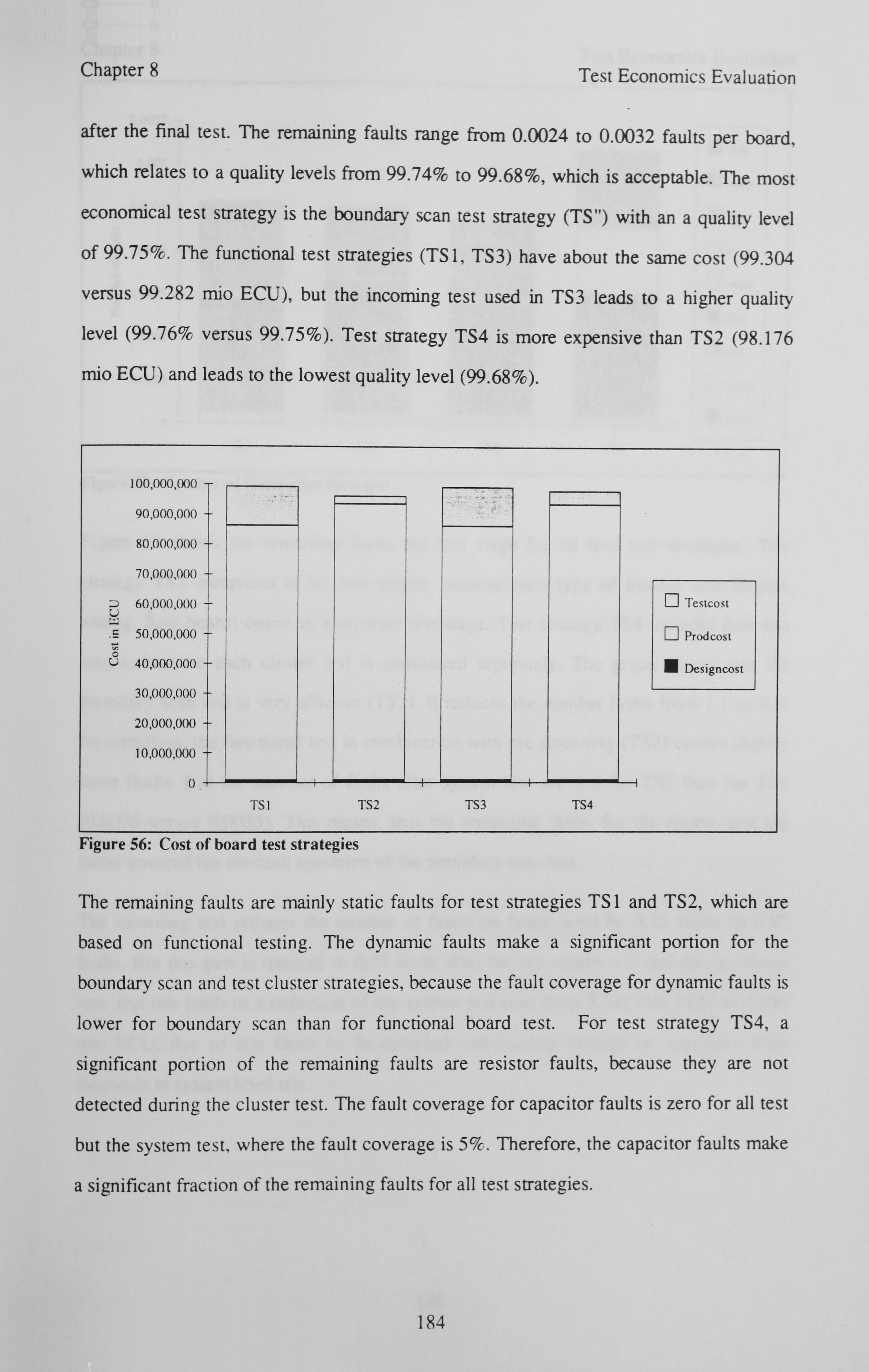
Chapter 8 Test Economics Evaluation
after the final test. The remaining faults range from 0.0024 to 0.0032 faults per board,
which relates to a quality levels from 99.74% to 99.68%, which is acceptable. The most
economical test strategy is the boundary scan test strategy (TS") with an a quality level
of 99.75%. The functional test strategies (TS 1, TS3) have about the same cost (99.304
versus 99.282 mio ECU), but the incoming test used in TS3 leads to a higher quality
level (99.76% versus 99.75%). Test strategy TS4 is more expensive than TS2 (98.176
mio ECU) and leads to the lowest quality level (99.68%).
100 000 0)0 , ,
90,000,000
80,000,000
70,000,000
60,000,000 U
Q Tcstcost
50,000,000 Q Prodcost 0 v 40,000,000 Designcost
30,000,000
20,000,000
10,000,000
0
TSI TS2 TS3 TS4
Figure 56: Cost of board test strategies
The remaining faults are mainly static faults for test strategies TS 1 and TS2, which are
based on functional testing. The dynamic faults make a significant portion for the
boundary scan and test cluster strategies, because the fault coverage for dynamic faults is
lower for boundary scan than for functional board test. For test strategy TS4, a
significant portion of the remaining faults are resistor faults, because they are not
detected during the cluster test. The fault coverage for capacitor faults is zero for all test
but the system test, where the fault coverage is 5%. Therefore, the capacitor faults make
a significant fraction of the remaining faults for all test strategies.
184

lý jýýJ jlDjJf( , iý. jý
Chapter 8 Test Economics Evaluation
0 0035 .
volt 0.003
® temp
0.0025 cap
0.002 Q
res
Q mem
0.0015
dyn
0.001 Ty '14 ýýp ýý `° `
Q � G ý , slat
0.0005 `ý'` open
short O
Ts l TS2 TS3 TS4
Figure 57: Number of faults after final test
Figure 58 shows the remaining faults per test stage for all four test strategies. Test
strategy TS3 comprises of six test stages, because each type of income test (digital,
analog, bare board) count as a separate test stage. Test strategy TS4 includes four test
stages, because each cluster test is considered separately. The graph shows that the
boundary scan test is very efficient (TS2). It reduces the number faults from 1.1 to 0.2.
Nevertheless, the functional test in combination with pre screening (TS2) covers slightly
more faults. But the number of faults after system test are less for TS2 than for TS I
(0.0026 versus 0.0025). This means, that the remaining faults for the system test are
better covered for the fault spectrum of the boundary scan test.
The incoming test reduces the number of faults on board level by 0.25 faults to 0.87
faults. But this gain is reduced to 0.02 faults after the pre screen test and the functional
test. But this leads to a reduction of the system test cost from 3.541 mio ECU to 3.250
mio ECU, due to less faults to be detected and located through an expensive fault
diagnosis at system level test.
185

Chapter 8 Test Economics Evaluation
1.2
1.1
" 0.9
0.8 TS I
0.7 --Cl- TS2
° 0.6 " TS3 E 0.5
z 0.4 0 TS4
0.3
0.2
0.1
0
Initial Testl Test2 Testa Test4 Tests Test6
Figure 58: Number of remaining faults per test stage
Figures 59 through 62 show per test stage the related cost per detected fault and the
fault coverage. The cost per detected fault include DFT cost as well as test application
cost. The fault coverage is calculated by the relation of the total faults which are detected
by the test.
The graphs show, that the prescreen test is a very efficient test, because it covers about
one third of the faults at low cost.
The functional test becomes very economical, if it is not applied to the complex VLSI
components, which is the case for the cluster tests. In all cases the fault coverage of the
functional test is more than 80% at reasonable cost per detected fault. But the boundary
scan test in TS2 achieves a higher fault coverage at about half the cost.
System test is in all test strategies very expensive. But it is needed, because it detects the
"hard faults", i. e. the faults which are hard to detect. Nevertheless a test strategy should
always avoid the slippage of faults to the system test, due to its high fault diagnosis cost.
The system test cost per fault for TS2 is much lower than for all other test strategies.
This is due to the boundary scan, which is used for fault diagnosis, and which reduces the
diagnosis cost. Additional DET cost is not included, because it is related to the board
level test.
186

Chapter 8 Test Economics Evaluation
The RAM self test in TS4 is very expensive, due to the high additional production cost,
which are caused by the expensive, self testable RAMs. In addition, the fault coverage is
very low, because it is limited to the faults which are related to the RAMs. For this
sample board, the self test of the RAMs is not an economical test strategy.
Summing up, it may be said, that a test stage, for which the fault coverage is low, but the
cost per fault is high, is a candidate to be removed. This is definitely the case for the
RAM self test in TS4, and eventually for the digital income test in TS3.
6,000 " 100%
90% 5,000
80%
70% 4,000
60%a
000 3 50% , C-
V. J " 40%p
2,000 30%
20% 1,000
-' ý 10%
0 0%
Prescreen Functional System
ý] cost per fault " fault coverage
Figure 59: Cost per detected fault in ECU per test stage for test strategy TSI
2,5(X) 100%
98%
96% 2000
.' l=` k"! ý ýR< 94%
1,500 90%
88% 1,000 86%
84%
500 ý"' _ 1" 82%
80%
0 78%
Boundarý" Scan System
cost per fault " fault coverage
Figure 60: Cost per detected fault in ECU per test stage for test strategy i , i-,
187
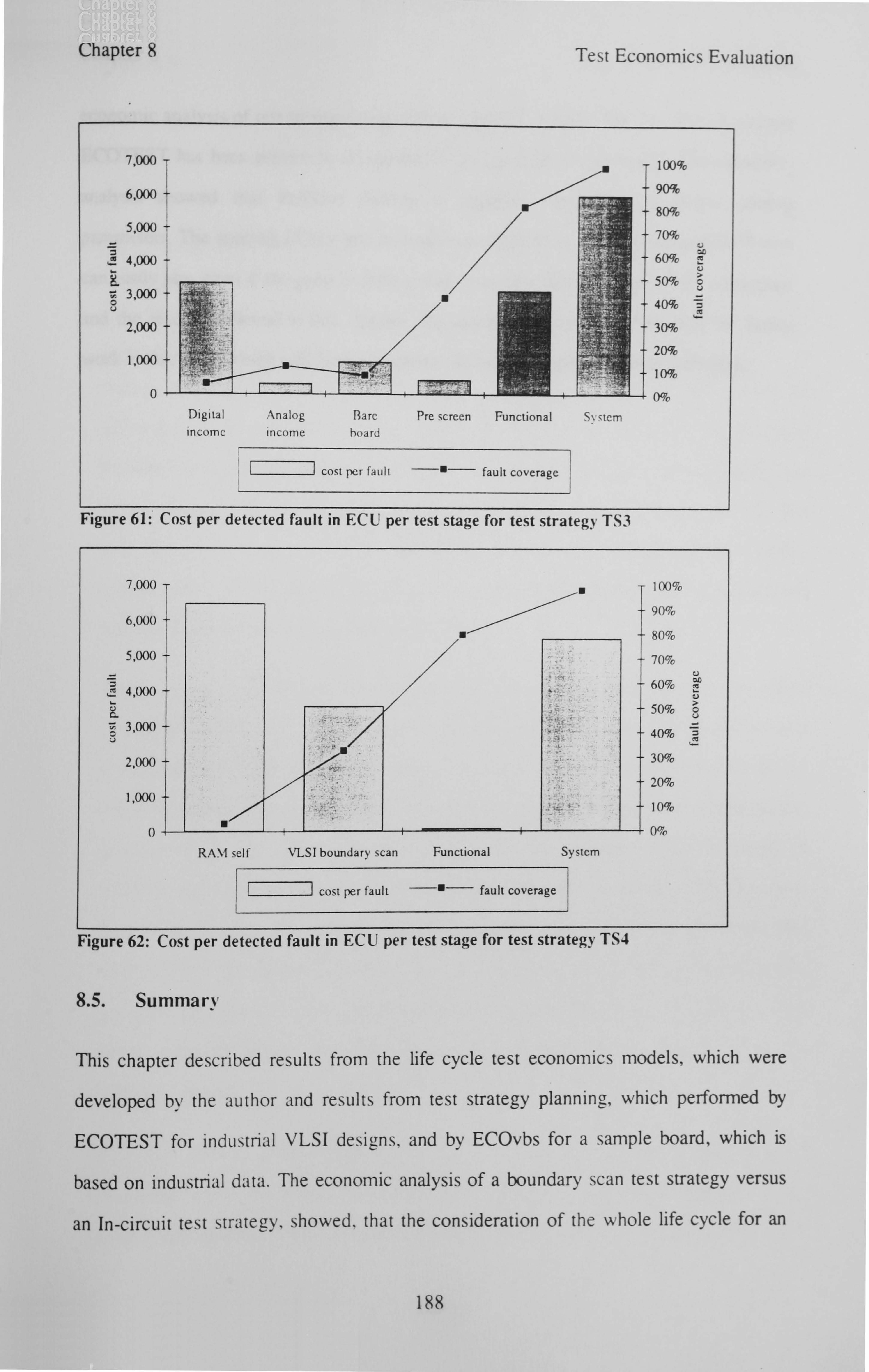
Chapter 8 Test Economics Evaluation
7,000 T 100%
6,000 k so%o
5,000 t 1 70'0 Yom.
4,000 60%
5090 > 3,000nr:..
40%
2,000 30%
20% 1,000,,,; &Lon
1090 "vt. { r
0 0%
Digital Analog Rare Pre screen Functional S\ ýtcm income income hoard
1 cost per fault " fault coverage
Figure 61: Cost per detected fault in ECU per test stage for test strategy TS3
7,00() T l (c)% 90%
6,000 80%
5,000 T 70%
4,000 60%
50% 0
V, 3.000 40%
2,000 " 30%
20% 1,000
10%
0 0%
RAM self VLSI boundary scan Functional System
ýý cost per fault " fault coverage
Figure 62: Cost per detected fault in ECU per test stage for test strategy, TS4
8.5. Summary
This chapter described results from the life cycle test economics models, which were
developed by the author and results from test strategy planning, which performed by
ECOTEST for industrial VLSI designs, and by ECOvbs for a sample board, which is
based on industrial data. The economic analysis of a boundary scan test strategy versus
an In-circuit test strategy, showed, that the consideration of the whole life cycle for an
188

Chapter 8 Test Economics Evaluation
economic analysis of test strategies may be an important aspect. The test strategy planner
ECOTEST has been proven to be applicable in industrial environments. The sensitivity
analysis showed that decision making is possible even with inaccurate costing
parameters. The analysis of four test strategies with ECOvbs showed, that high DFT cost
can easily pay, even if the gains in field test are not considered. Based on the experience
and the results achieved in this chapter, the author will present some ideas for future
work in this field, which will further improve the tools for optimising test strategies.
189

Chapter 9
Chapter 9
Conclusions
9.1. Summary of the Work
Conclusions
This thesis described a novel approach for creating test strategies for complex, VLSI
based systems. It presented previous work in this field, which is mainly related to test
strategy planning for ICs and not boards or entire systems. The author has discussed the
advantages of his approach over previous systems. The test strategy planning system
described is based on life cycle economic evaluations, which defines a test strategy for
the life cycle of the entire system instead of limiting it to a certain integration level. The
evaluation of the economics of test strategies is based on predictions, which are subject
to inaccuracy. A method for evaluating and handling this inaccuracy was developed and
integrated into the test strategy planning system.
The test strategy planning system comprises of two software tools, which can be linked
to each other, and which can be used by different groups of persons. ECOTEST is a test
strategy planner for heterogeneous ASICs, which enables to create test strategies for the
cell based ASICs. The test strategies can be generated automatically, semi automatically,
or interactively. The system can generate different test strategies which are based on
different requirements, such as different achievable fault coverages. The economic
parameters of these different test strategies can then be used in ECOvbs, the test strategy
planner for VLSI based systems. The IC level test strategies are used as part of the life
cycle test strategies, and the related economics during the life cycle of the entire system
can be evaluated. In the same way. a board level test strategy is integrated into the life
cycle test strategy.
Both test strategy planners are based on a test economics model and on stored
knowledge about the impact of test methods on the economics parameters (the test
method descriptions). The test economics model and the test method descriptions can be
190

Chapter 9 Conclusions
altered by the user of the system. The system is implemented by an object oriented
approach in C++.
9.2. Conclusions
The results, which are presented in chapter 8 and the usage of the system in industrial
environments by users other than the developers of the system showed that the
approaches and the implementation are satisfactory.
The sensitivity analysis methods removed a problem, which has led to concerns about the
test economics approach by several test experts. By handling the costing parameters as
variates, the inaccuracy of predicting values for the primary parameters as well as the
inaccuracy of the test economics model itself is taken into account by determining its
impact on the inaccuracy of the total cost. The decision criterion of minimising the total
cost is then replaced by minimising the worst case of the total cost in a user defined
percentage of cases. This method allows to select between a certain probability to get
very low cost by a high risk to get very high cost and a high probability to get moderate
cost with a low risk to get very high cost.
Another concern about the test economics modelling approach for test strategy planning
was addressed to the cost of data gathering. This problem has been partly solved by
refining the complex test economics model, which was developed at Brunel University
([Var84], [Dis92]), by removing some parameters not necessarily important in industrial
uses. In addition, the sensitivity analysis method can also be used for reducing the cost
for data gathering. The related approach, which was developed by the author, is called
iterative sensitivity analysis. This method allows to start test strategy planning with a
rough but cheap estimate of the primary parameters. The outcome of the sensitivity
analysis is then used to analyse, which parameters are more and which are less sensitive.
Based on this result, a more accurate parameter prediction can be performed, but only
for the sensitive parameters.
191

Chapter 9 Conclusions
The partitioning of the system into two separate tools allows the usage by two different
group of persons. This matches to the organisation of most electronic companies. A
quality assurance department is responsible for test strategy planning for systems,
whereas the ASIC designers are responsible for the IC level test strategy. Nevertheless,
the quality assurance people get more and more interested in design-for-testability
strategies, but their knowledge about these methods and its impact on the economics is
often poor. This partitioning of the test strategy planning allows it to be used by the
designers for generating alternative IC test strategies. The economic results can then be
used by the quality assurance people in order to evaluate the economics of incorporating
the DFT strategies into a test strategy for the entire system.
The test strategy planning system was used in different industrial environments, and it
was applied to different industrial designs. The feedback coming from the industrial
users, which came from different companies in different countries with a different
business (T. I. D. in Spain, Philips in the Netherlands, Bull in France, Siemens, Telefunken
and SNI in Germany), showed, that the test strategy planning system is a useful tool for
solving the problem of test strategy planning. The discussions with the users showed the
big interest in the methods of economics based decision making and the way this method
is implemented in the test strategy planning system. These discussions and the study of
the future needs in the field of design and production of complex electronic systems have
led to the following ideas, which could extend the approach of economics based test
strategy planning, and which could further improve the system.
9.3. Future Research
The test strategy planner ECOTEST is based on a fixed hierarchy of the design. The
testable units are defined by the hierarchy of the design. The partitioning of the design
into testable units is not always straightforward, and different partitioning leads to
different test strategies with different economics. To evaluate the different partitioning of
the design with ECOTEST, the design must be repartitioned by the user. This can cause
192

Chapter 9 Conclusions
a significant effort, especially if many different partitioning should be evaluated. Also,
this method does not allow for automatic generation of the optimum partitioning. For
these reasons, an extension of the system, which allows an online partitioning of the
design, either by the user or automatically by the system, could lead to a further
improvement of ECOTEST.
Test strategy planning in ECOvbs is not performed automatically. This is not a critical
weakness, because test strategies can be set up by the user very quickly, and the system
allows for parallel evaluation of alternative test strategies. But an automatic evaluation of
test strategies by evaluating all possible combinations, or a user defined subset of it, can
be an improvement of the system for cases where the number of test strategy alternatives
is very large, or if there are economical alternatives, which are not taken into account by
the user for certain reasons.
Other enhancements of the system are mainly related to integrating it into other
environments. ECOTEST in its current version is a pure advisory tool. The
implementation of the test strategy, especially the implementation of the DFT techniques
is not linked to ECOTEST. Today's design methodology includes more and more logic
synthesis which allows to describe the design on a higher level than gate level. A
description of DFT techniques on this higher level could be formulated independent of
the design. This DFT synthesis description can be part of the test method descriptions of
ECOTEST, which allows to link ECOTEST to logic synthesis tools. The DFT part of
the generated test strategy is then implemented automatically by a push-button link from
ECOTEST to the synthesis tool.
The test strategy planner ECOvbs takes into account many production data, which may
be available in a computer integrated manufacturing data base (CIM). By integrating
ECOvbs into such a CIM environment, many data could be accessed directly from its
source. This reduces the cost of data gathering and makes the provision of data more
secure, especially concerning data updates and data entering errors.
193

Chapter 9 Conclusions
The methods of economics driven test strategy planning, which have been developed by
the author, are very general. They can easily be adopted for other applications of
engineering decision making. In the introduction it was shown that test strategy decisions
are tightly linked to design and manufacture decisions. This fact can be used in
integrating other decision making processes, such as technology decisions, or
manufacturing strategies, into the economics based test strategy planning system. This
would extend the test strategy planning system in an engineering decision making system,
which would provide a real concurrent engineering tool.
The complex problem of test strategy planning for VLSI based systems has mainly been
solved by the approach which has been described in this thesis. Using this system will
help to avoid the development of untestable and therefore non sellable electronic
systems. The system helps in particular to minimise the expenditures which are needed to
assure a high quality of the systems which are shipped to the customers. This work has
attracted significant attention by industry. This attention has made the author optimistic,
that the approach will be used extensively in the future, and that other applications for
this approach, as discussed in the previous section, will arise soon.
194

References
References
[Aba89] Abadir, M.:
TIGER: Testability Insertion Guidance Expert System
Proc. IEEE International Conference on CAD, 1989
[Abr84] Abramovici, M., Menon, P. R., Miller, D. T.:
Critical Path Tracing : AN Alternative to Fault Simulation.
IEEE Design & Test of Computers, 1/1984
[Aga90] Agarwal, V.:
Comment on the presentation "Planning Testable VLSI Design under
Economic Aspects"
Workshop "Testmethoden und Zuverlässigkeit von Schaltungen und
Systemen", 1990
[Agr82] Agrawal, V. D., Mercer, M. R.:
Testability Measures: What Do They Tell Us?
Proc. ITC 1982
[And80] Ando, H.:
Testing VLSI with Random Access Scan.
Dig. COMPCON 1980
[Ant82] Antreich, K. J., Koblitz, R. K.:
Design Centering by Yield Prediction
IEEE Transactions on Circuits and Systems, vol. CAS-29, no. 2, February
1982, pp. 88-95
[Ant87] Antreich, K. J., Schulz, M. H.:
Accelerated Fault Simulation and Fault Grading in Combinational Circuits.
IEEE Transactions on CAD, vol CAD-6, Sept. 1987
[Ard871 Ardeman, A.:
ASICs: Costing and Planning
Nev Electronics, 20 January 1987
195

References
[Arm72] Armstrong, D. B.:
A Deductive Method for Simulating Faults in Logic Circuits.
IEEE Transactions on Computers, 21/1972
[Arm82] Armaos, J.
Zur Optimierung elektrischer Schaltungen unter Berücksichtigung der
Parametertoleranzen.
PhD thesis, Institute for Computer Aided Circuit Design, Technical
University of Munich, 1982
[Bar92] Bartesch, V.:
CAE - Verfahren zur Auswahl und Bewertung von Selbsttestmethoden
Diploma thesis at Fachhochschule Muenchen, Fachbereich Elektrotechnik,
1992
[Bee89] Beenker, F., Dekker, R.:
General Introduction to the Philips Macro-Test Concepts.
EVEREST report, Doc. No. PHI 0062 TN 01 IN WP5
[Bee90] Beenker, F., Dekker, R., Stans, R., Van der Star, M.:
Implementing Macro Test in Silicon Compiler Design
IEEE Design&Test of Computers, April 1990, pp. 41-51
[Be161 ] Bellman, R.:
Adaptive control processes: A guided tour
Princeton University Press, 1961
[Ben80] Bennetts, R. G., Maunders, C. M., Robinson, G. D.:
CAMELOT: A Computer-Aided Measure for Logic Testability.
Proc. ICCD 1980
[Ben84] Bennetts, R. G.:
Design of Testable Logic Circuits.
Addison-Wesley Publishing Company. 1984
196

References
[Ben87] Bennetts, R. G.:
Evaluating the cost of using an ATE -a structured approach
Computer-Aided Engineering Journal, August 1987
[Ben89] Bennetts, R. G.:
Definition of basic terms used in testing, and a list of abbreviations used in
WP5.
ESPRIT - EVEREST report no. BEN0026 TN 01 IN W5
[B1a78] Blanchard, B. S.:
Design and Manage to Life Cycle Cost
M/A Press, Portland, 1978
[B1o88] Blohm, H., Lueder, K.:
Investition
Verlag Vahlen, Muenchen 1988,6th edition
[Brg84] Brglez, F.:
On Testability Analysis of Combinational Networks.
Proc. ISCAS 1984
[Brg89] Brglez, F.; Bryan, D.; Kozminski, K.:
Combinational Profiles of Sequential Benchmark Circuits.
Proceedings of Int. Symposium on Circuits nad Systems, 1989
[Che89] Cheng, K. T., Agrawal. V. D.:
Design of Sequential Machines for Efficient Test Generation
Proc. IEEE International Conference on Computer-Aided Design, 1989, pp
358-361
[Dae81 ] Daehn. W., Mucha, J.:
A Hardware Approach to Logic Testing of Large Programmable Logic
Arrays.
IEEE Trans. on Computers, vol. C-30, Nov 1981, pp 829-833
197

References
[Das82] Das Gupta, S., Goel, P., Walther, R. G., Williams, T. W.:
A Variation of LSSD and Its Implication on Design and Test Pattern
Generation in VLSI.
Proc. ITC 1982
[Dav82] Davis, B.:
The Economics of Automatic Testing
McGraw-Hill, 1982
[Dav92] Davis, B.:
The economics of design and test
in Proc. Economics of Design and Test for electronic circuits and systems,
Ellis Horwood Limited, Chichester, 1992
[Dea89] Dear, I. D. D.:
Test Strategy Planning Methodology for the Functional Testing of Integrated
Circuits that is Driven by Economic Parameters.
PhD thesis, Brunel University, 1989
[Dic87] Dick, J.:
Entwicklung und Implementierung eines Programmes zum Erkennen
redundanter Fehler in kombinatorischen Schaltungen.
Master thesis at Technische Universität München, Lehrstuhl für
Rechnergestützes Entwerfen, 1987
[DiG89] Di Giacomo, J.:
VLSI Handbook.
McGraw Hill publishing Company, 1989
[Din69] Dinkelbach, W.:
Sensitivitätsanalysen und parametrische Programmierung
Springer Verlag Berlin Heidelberg New York, 1969
[Din82] Dinkelbach, W:
Entscheidungsmodelle
Walter de Gruyter Verlag Berlin New York, 1982
198

References
[Dis89] Dislis. C., Dear, I. D., Miles, J. R., Ambler, A. P.:
Cost Analysis of Test Method Environments
Proc. IEEE Intenational Test Conference, 1989
[Dis9l] Dislis, C., Dear, I. D., Ambler, A. P.:
An Economics Based Test Strategy Planner for VLSI Design
Proc. European Test Conference, 1991
[Dis92] Dislis, C.:
A Financially Based Automated Advisor for Design for Test Strategy
Generation.
PhD thesis, Department of Electrical Engineering and Electronics, Brunel
University, 1992.
[Eic77] Eichelberger, E. B., Williams, T. W.:
A Logic Design Structure for LSI Testability.
Proc. Design Automation Conference 1977
[Eic8O] Eichelberger, E. B. and Lindbloom, E.:
A Heuristic Test Pattern Generator for Programmable Logic Arrays.
IBM J. Research and Development, vol. 24, Jan. 1980, pp 15-22
[Fuj83] Fujiwara, H., Shimono, T.:
On the Acceleration of Test Generation Algorithms.
IEEE Transactions on Computers, 32/1983
[Gho89] Ghosh, A., Devadas, S., Newton, A. R.:
Test Generation for Highly Sequential Circuits.
Proc. ICCAD 1989
[Goe8O] Goel. P.:
Test Generation Costs Analysis and Projections.
Proc. Design Automation Conference, 1980
199

References
[Goe8l] Goel, P.:
An Implicit Enumeration Algorithm to Generate Tests for Combinational
Logic Circuits.
IEEE Transactions on Computers, 30/1981
[Go180] Goldstein, L. H., Thipgen, E. L.:
SCOAP: Sandia Controllability/Observability Analysis Program.
Proc. DAC 1980
[Gra79] Grason, J.:
TMEAS -A Testability Measurement Program.
Proc. Design Automation Conference 1979
[Gun90] Gundlach, H. H. S., Mueller-Glaser, K. D.:
On Automatic Test Point Insertion in Sequential Circuits
Proc. IEEE International Test Conference, 1990, pp. 1072-1079
[Ham65] Hammersley, J. M., Handscomb, D. C.:
Monte Carlo Methods
Methuen & Co. Ltd., London, 1965
[Hey89] Heymbeeck, L.:
A Literature Survey of Functiona1/Behavioral Testing.
EVEREST report DOC. No. PHI 0066 SS TN
[Hi185] Hills, T. G., Davis, M. J., Rogers, W. E.:
Cost Visibility Through Life Cycle Cost Boards.
Logistics Spectrum, vol. 19, Los Angeles 1985, pp. 23-25
[Hwa86] Hwang, K. S., Mercer, M. R.:
Derivation and Refinement of Fanout Constraints to Generate Tests in
Combinational Logic Circuits.
IEEE Transactions on Computer Aided Design, vol. CAD-5, no. 4, Oct.
1986
200

References
[I1186] Illman, R. J.:
Design of a self testing RAM.
Proc. Silicon Design Conference, 1986, pp 439-446
[I1189] Illman, R.:
Reviewers Report
Review of the ESPRIT project EVEREST, 1989, Munich
[Keu93] Keutner, K.:
SPLASH: A Highly Efficient Path Sensitization Method for
Algorithmic/Structural Hardware Descriptions
submitted to IEEE Design&Test of Computers
[Kir79] Kirk, S. J.:
Life Cycle Costing: Problem Solver for Engineers
Specifying Engineer, Washington D. C. 1979, pp. 123-129
[Kje8I] Kjellstrom, G., Taxen, L.:
Stochastic Optimization in System Design.
IEEE Transactions on Circuits and Systems, vol. cas-28, No. 7, July 1991
[Koe79] Koenemann, B., Mucha, J., Zwiehoff, G.:
Built-In Logic Block Observation Techniques
Proc. IEEE Test Conference, 1979
[Kov81 ] Kovojanic, P. G.:
Single Testability Figure of Merit.
Proc. ITC 1981
[Kre75] Kreyszig, E:
Statistische Methoden und ihre Anwendungen.
Vandenhoeck & Ruprecht Verlag Göttingen, 5th edition, 1975
(Kub84] Kuban, J. R.. Bruce. W. C.:
Self Testing the Motorola MC 6804P2.
IEEE Design & Test, vol. 1, no. 2, May 1984
201

References
[Laf91 ] Laffitte, M.:
Interactive Test Strategy Planning: A Model and a Prototype.
Proc. European Test Conference, 1991
[Lar89] Larrabee, T.:
Efficient Generation of Test Patterns Using Boolean Difference.
Proc. ITC 1989
[Lue73] Luenberger, D. G.:
Introduction to Linear and Nonlinear Programming.
Addison Wesley Publishing Company, Reading Massachusetts, 1973
[Mad841 Madauss, B. J.:
Projektmanagement
2nd edition, Stuttgart 1984
[Mar86] Marlett, R. A.:
An Effective Test Generation System for Sequential Circuits.
Proc. DAC 1986
[McC86] McCloskey, E. J.:
Logic Design Principles
Prentice-Hall International Editions, 1986
[Mi191 ] Miles, J., De Bondt, R., Daemen, L.:
A Test Economics Model and Cost Benefit Analysis of Boundary Scan
Proc. European Test Conference, 1991
[Mye831 Myers. M. A.:
An Analysis of the Cost and Quality Impact of LSI/VLSI Technology on
PCB Test Strategies
Proc. IEEE International Test Conference, 1987, pp. 382-395
[Oh187] Ohletz. M. J., Williams,. T. W., Mucha, J. P.:
Overhead in Scan and Self-Testing Designs.
Proc. ITC 1987
202

References
[Pab87] Pabst, J. S.:
Elements of VLSI Production Test Economics.
Proc. IEEE International Test Conference, 1987, pp. 982-986
[Poa63] Poage, J. F.:
Derivation of Optimum Tests to Detect Faults in Combinational Circuits.
Proc. Symposium on Mathematical Theory of Automata, Polytechnic Press,
New York 1963
[Pyn86] Pynn, C.:
Strategies for Electronics Test.
McGraw-Hill, 1986
[Rat82] Ratiu, I. M.:
VICTOR: A Fast VLSI Testability Analysis Program.
Proc. ITC 1982
[Rei83] Reinertsen, D. G.:
Whodunit? The search for the new-product killers.
Electronic Business, vol. 11, July 1983, pp. 106 - 109
[Rog85] Rogers, W. A., Abraham, J. A.:
CHIEFS: A Concurrent, Hierarchical and Extensible Fault Simulator.
Proc. ITC 1985
[Rot66] Roth. J. P.:
Diagnosis of Automata Failures: A Calculus and A Method.
IBM Journal of Research & Development, vol. 10, July 1966
[Rot8O] Roth, J. P.:
Computer Logic, Testing, and Verification.
Computer Science Press 1980
[Rot89] Roth, W., Johansson, M., Glunz, W.:
The BED Concept: A Method and a Language for Modular Test Generation
Proc. International Conference on VLSI, 1989, pp. 143-152
203

References
[Rub86] Rubinstein, R. Y.:
Monte Carlo Optimization, Simulation and Sensitivity of Queueing Networks
John Wiley & Sons, New York 1986
[Saa6l] Saaty, T. L., Webb, K. W.:
Sensitivity and renewals in scheduling aircraft overhaul.
Proceedings of the Second International Conference on Operational
Research, pp. 708-716, English University Press, 1961
[Sa185] Saluja, K. K., Kinoshita, K., Boswell, C.:
A Design of Parallel Testable Programmable Logic Arrays.
Tech. report EE8501 Dept of Electrical and Computer Eng., Univ. of
Newcastle, NSW, 2308, Australia, 1985
[Sch76] Schmitz, N. and Lehmann, F.:
Monte-Carlo Methoden 1
Verlag Anton Hain, Meisenheim am Glan, 1976
[Sch841 Schuster, M. D., Bryant, R. E.:
Concurrent Fault Simulation of MOS Digital Circuits.
Proc. Conf. Advanced Research in VLSI 1984
[Sch88] Schulz, M. H., Trischler, E., Sarfert, T. M.:
SOCRATES: A Highly Efficient Automatic Test Pattern Generation System.
IEEE Transactions on Computer-Aided Design, Jan. 1988
[Sed92] Sedmak, R.:
Economics and Other Management Issues
Design for Testability Training Course, held at Texas Instruments, Munich,
199?
[Se1681 Sellers, E. F., Hsiao, M. Y., Bearnson, L. W.:
Analysing Errors with the Boolean Difference.
IEEE Transactions on Computers 1968, pp. 676-683
204

References
[Ste77] StewartH. J.:
Future Testing of Large LSI Circuit Cards.
Dig. IEEE Semiconductor Test Conference 1977
[Su84] Su, S., Lin, T.:
Functional Testing Techniques for Digital LSI/VLSI Systems.
Proc. DAC 1984
[Szy92] Szygenda, S. A.:
Profit, liability, and education: Influencing factors on the economics of non-
testing
in Proc. Economics of Design and Test for electronic circuits and systems,
Ellis Horwood Limited, Chichester, 1992
[TEN921 Siemens-Nixdorf:
TENaphro user manual, 1992
[Tre85] Treuer, R., Fujiwara, H., and Agrawal, V. K.:
Implementing a self test PLA design.
IEEE Design and Test of Computers, vol. 2, Apr. 1985 pp 37-48.
[Tri821 Trischler. E.:
Scan Structures Study.
Siemens Report No. RTL-82-TR-003,1982
[Tri83] Trischler, E.:
Testability Analysis and Incomplete Scan Path
Proc. IEEE International Conference on Computer Aided Design, 1983,
pp. 8-39
[Tri84] Trischler. E.:
ATWIG: An Automatic Test Pattern Generator with Inherent Guidance.
Proc. ITC 1984
[Tsu871 Tsui. F. F.:
LSI/VLSI Testability Design.
McGraw-Hill Book Company, 1987
205
References
[Tur9O] Turino, J.:
Design to Test.
2nd edition, Van Nostrand Reinhold, New York, 1990
[Var84] Varma, P., Ambler, A. P., Baker, K.:
An Analysis of the Economics of Self-Test.
Proc. IEEE International Test Conference, 1984
[Wai85] Waicukauski, J. A., Eichelberger, E. B., Forlenza, D. B., Lindbloom, E.,
McCarthy, T.:
A Statistical Calculation of Fault Detection Probabilities by Fast Fault
Simulation
Proc. ITC 1985
[Wi183] Williams, T. W., Parker, K. P:
Design For Testability -A Survey
Proc. IEEE, vol. 71, pp 98-112, Jan 1983
[Wue841 Wuebbenhorst, K.:
Konzept der Lebenszykluskosten
Verlag fuer Fachliteratur, Darmstadt, 1984
[Zhu86] Zhu, X.:
A Knowledge Based System for Testable Design Methodology Selection
[Zhu88] Zhu, X., Breuer, M.: Analysis od Testable PLA Designs IEEE Design
& Test of Computers, vol. 5, no. 4, Aug 1988, pp. 14-28
Proc. DAC 1982
PhD -
206

Appendix A
Determination of Correlation Coefficients
In chapter 6 the author has described and performed several sensitivity analysis
techniques for cost models which are all based on variates as input parameters. Most of
the input parameters are independent from each other, but some of them are correlated.
Due to being pairwise correlations, the related variates can be generated by using the
correlation coefficients.
In this appendix. the author will describe the method to derive the correlation
coefficients, and the correlation coefficients will be derived from statistical data for the
correlations between the gate count and the number of cells, the gate count and the
number flip flops and between the number of flip flops and the sequential depth.
1. Algorithm to Determine Correlation Coefficients
Based upon a table of values for two variates X and Y with expectations of uX and py
and variances of ßX= and ßy2, which are correlated, the correlation coefficient can be
determined as follows:
" determine the covariance of X and Y:
ßi. 1, = E([X-4x]-[Y-4y])
where E() stands for the expectation or the mean value of the term in brackets.
0 calculate the correlation coefficient by
P= 6t

2. Calculation of Correlation Coefficients
We have received data about the gate count and the related cell count for 21 standard
cell designs, which were designed at Siemens. The data are presented in table 1. Design Gates Cells
SIEZ 2085 485
SIEZ 2000 300
SIES 1000 200 SIE4 3922 2.500
SIE5 7717 1844
SIF6 19): ; 1022
SIE7 5493 1025
SIES 14S06 4076
SIE9 4207 12
SIE10 15418 3005
SIEHT 13849 2723
SIE12 45028 4274
SIE 13 _799O 4095
SIE14 33042 1807
SIE 1S =64 27
SIE16 326 98
SIE17 3881 787
SIELS 4872 1520
SIEI9 1685 675
SIE20 3096 1062
SIE21 217 46
u ý> 183.476 1503.95 _381
6 1 181 . 59 1422.973172
134792-1.2Z IP 0.777614131
Table 1: Gate count and related number of cells for Siemens
standard cell designs
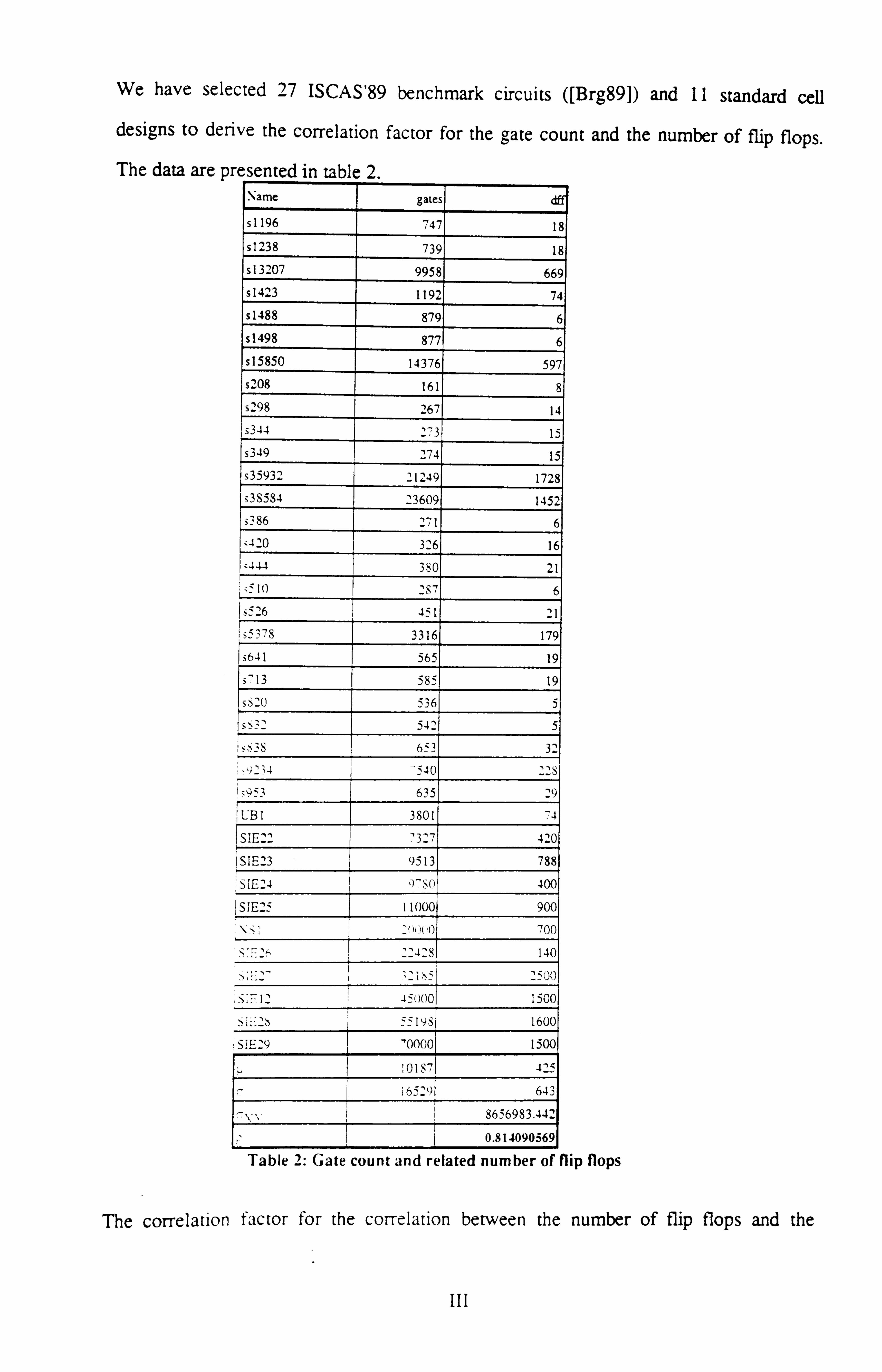
We have selected 27 ISCAS'89 benchmark circuits ([Brg89)) and 11 standard cell designs to derive the correlation factor for the gate count and the number of flip flops.
The data are presented in table 2. Name gate s dff
s1196 74 7 18
s1238 73 9 18
s13207 995 8 669
s1423 119 2 74
s1488 87 96
s1498 877 6
s15850 14376 597
s208 161 8
s2298 267 14
s344 273 15
s349 274 15
s35932 21249 1728
s3S534 23609 1452
s386 2-11 6
420 326 16
444 380 21
X 10 : S7 6 1-6 351 21
`378 3316 179
s641 565 19
s713 585 19
s820 536 5
542 5
3S 653 32 1234
-540 -128
H953 635 29
UB 1 3801 74
SIE22 7327 420
SIE23 9513 788
S IE24 ß, S() 400
SIE25 11000 900
000 700
ý. ,ý �t=3 140
i` '_500
1_ a5000 1500
S 2s 111981 1600
SiE_9 '0000 1 1500
10181, 425
16529 613
-ý ", I 8656983.442
0.814090569
Table 2: Gate count and related number of flip flops
The correlation factor for the correlation between the number of flip flops and the

sequential depth for the circuits in table 3 was derived by calculating the average number
of test patterns per target fault which were generated by SNI's sequential ATPG system
TENace and by setting the sequential depth to that value. Circuit #dff seq. depth
s'08 8 2.29
s298 14 5.86
s344 15 2.95
s349 15 2.84
s386 6 1.69
s444 21 9.85
s641 19 1.33
s713 19 1.37
s1 196 18 1.25
s1238 18 1.16
15.3 3.06
4.90 2.77
_Xy 3.087311
p 0.227071
Table 3: Number of Flip flops and related sequential depth
On the basis of the calculated correlation factors, the following values were used for the
sensitivity analysis in chapter 6:
Pcell: 0.78
Pflipflop= 0.81
Pseqdepth: 0.2 3
IV

Appendix B
Listing of the Cost Models
Siemens Nixdorf
Appendix B: Cost Model Parameters and
Syntax of Equations
In the following the syntax for describing equations is listed. The meta language used here in the one of the UNIX tool YACC.
equation :" (" equation ") "I
equation "+" equation equation "-" equation equation equation equation "-" equation equation "%" equation equation " equation equation equation equation equation equation ">" equation
" -" equation "+" equation equation "! " equation "? " equation ": " equation
function double
parameter in_var
double : double constant function :" @LOG 10" " (" equation ") "
"@PUC" " (" equation ")"
fname " (" par-list fname " (" ") "
par-list
equation equation ", " par-list
parameter : NAME in_var: one of the design identifiers listed in chapter 8.5
Definition of the parameters In the following list the cost model parameters are defined by its internal name and the
data type of its value. Two signs have special meanings:
36 User Manual

Siemens Nixdorf
- The " ̀ " means, that this parameter is expanded for an application to the number of TUs in the design by copying the internal name and indicating it by consecutive numbers.
The meaning of the parameters will be described later.
1) Design Indenendant Primary Parameters Identifier Data Type kdes float kp float
cexp float hpw float
exper int
pcad float descentrate float
equrate float
costrate float fpg float
fcv float
2) Cost-Model Desi gn-Dependant Primary Parameters Identifier Data Type
nre float
vol int
percuse float
cputime float fcreq" float tpf" float tpver float
pms int
pps float Cost-Model Test-Dependant Primary Parameters
Identifier Data Type
numtp_normal int
numtp_scan int
numtp_self int
cells" int
in int
out int bi int
cperf" float
37 User Manual

Siemens Nixdorf
or" float
cgate" int avs" float
costtgs" float fcach" float
Secondary parameters Identifier data type equation puc float @PUC
PC plib pdes prod cpin Icompl"
ocompl mp engcost descentcost
mainframecost descost faults" faults
remfaults" mtgtime" mtc faultsa"
numtpa"
numtpm" tpgen"
tsl
tac tcost ovcost
int nre+vol * puc float 1 /cells float 1-1 /(kdes+exper)
float kp * pcad * pdes * plib int 2* in+out+3 * bi float cperf" * (1-or") * cgate" float cpin * IcomplAcexp float compl/prod float mp * costrate float percuse * destime * descentrate float cputime * equrate float engcost+descentcost+mainframecost int cgate" * fpg int faults& float ` ((fcreq"-fcach")>0) * (fcreq"-fcach") *faults
float remfaults" *tpf"/hpw
float mtgtime * costrate int ((fcachr-fcv)>O) * (fcach"-fcv) *faults-
int faultsa" * tppf * (avs`+1)
int remfaults" * (avs"+1)
int numtpa"+numtpm" int tpver + numtp_normal + numtp_scan + numtp_self
float (tsi-tsl%pms)/pms * pps * vol float tac+mtc+costtgs float pc+descost+tcost+ttmcost
Tr-- I. - . I- - 38 User Manual

Siemens Nixdorf
Description of the Parameters:
1) Design Independant Primary Parameters kdes: Normalising factor, which normalises the designers experience. The factor normalises the productivity of a designer with no experience related to the productivity of most experienced designer. See equation for pdes XAL Linear factor to normalise the design time.
cex : Exponent to derive the design complexity from the gatecount hpw: Working hours per week ex er: Designer" s experience in number of designs he has already performed pcad: Productivity of the CAD system as a linear paramater of the design time descentrate: Cost rate of hiring a design center per week e uq rate: Accounted cost per CPU-hour for the usage of mainframe computers costrate: Weekly cost rate of designer fQg
Average number of stuck-at faults per gate fcv: Typical fault coverage achieved by verification patterns
2) Design-Dependant Primary Parameters
nre: Non-recurring engineering cost, accounted by the silicon producer
vol: Production volume percuse: Percentage of design time, a accounted design center is used
cputime: CPU time in hours, an accounted equipment is used
TFMt; n vn 1 39 User Manual

Siemens Nixdorf
fcr eg Required fault coverage per TU tpff"_ Time needed to get a test pattern set for testing a single fault by hand tpver: Number of test patterns for verification pms" Number of test patterns, for which the price for test application increases steplike pps: Price per additional test pattern set per device
costtgs: Cost for ATPG
3) Test-Dependant Primary Parameters
avs" : Average sequential depth per TU; here the typical number of clock cycles (or
patterns) is meant for controlling and observing internal nodes. numtp_normal: number of test patterns per chip to be applied by a test equipment numtp_scan: number of scannable test patterns per chip to be applied by a test equipment
numtp=self: number of self test patterns per chip to be applied
puc: Production unit cost cells: Number of cells in: Number of input pins out: Number of output pins bi:
Number of bidirectional pins cperf: Performance complexity; the performance implication is a linear cost factor
whose value range is between 1 and co .A value of 1 indicates the uncritical case
whereas co means, that it is impossible to perform the design. For example, a
factor of '2' doubles the design time.
Tr-L 11--- 110% - 40 User Manual

Siemens Nixdorf
or: Originality; this linear parameter describes, whether some of the architecture, functions or algorithms have been developed before, and in what way this knowlegde accelerates the design process. The value must be in between 0 (design is fully original) and 1 (the TU has already been designed). c gate-: Equivalent gate count per TU, derived from the equivalent gatecount of the cells used; this parameter is a complexity measure as well for estimating the design time as for estimating the test pattern generation cost. In addition, the production unit cost are derived from this parameter. agate: Equivalent gate count of chip; this value is simply the sum of the TU's gatecounts.
4) Secondary Parameters
Q-CL Production cost
l
Productivity of the cell library used; by this parameter it is calculated, how well the
cell library fits to the design.
Ades: The experience of the designer; this parameter is based upon the number of designs, the designer has already performed prod: Overall productivity, composed of productivity of the cell library, productivity of the
CAD system and the experience of the designer.
spin: Pin complexity compl: Overall complexity, composed of performance complexity, pin complexity,
originality and the equivalent gatecount.
M. Design effort in weeks numdes: Number of designer needed
engcost: Engineering cost of the design
descentcost: Cost for hiring a design center
mainframecost:
TAM, +;., %In , 41 User Manual
Siemens Nixdorf
Cost for using computers accounted for CPU-time descost: Overall design cost faults: Number of possible stuck-at faults on chip fcach: Achievable fault coverage by ATPG
remfaults: Number of aborted faults from ATPG
mt time: Time needed for manual TPG
mtc: Overall cost for manual TPG faultsa: Number of faults, for which test patterns were generated by the ATPG system
numtpa: Number of test patterns per TU generated by the ATPG system
numtpm: Number of test patterns generated by hand
ttpgen: Number of generated test patterns tsl: Number of overall test patterns (test set length)
tac: Test application cost tcost: Overall test cost ovcost: Overall or final cost
Tr=n, +;,, �r) 1 42 User Manual

Doc. Ref.: \EVEREST\SIE\WP3\036
EREST Doc. Ext.: TN 01 AP Page: 1
EVEREST Activity Report Task ID: 095
Activity: 3.2.4. b
Test Economics Model Development
CEC Deliverable: No
Distribution: Free
Authors: pochen wick, SNI AG
Approved: Francis Gourdy, Bull S. A.

Doc. Ref.: \EVEREST\SIE\WP3\036
EVEREST Doc. Ext.: TN 01 AP Page: 2
Table of Contents
1. Introduction ................................................ 3
2. The phase model of a VBS life cycle .......................... 4
3. Model overview ............................................. 6
4. A model of the cost of PCBs ................................. 8
4.1 A model of the development costs ......................... 8
4.2 A model of the production costs .......................... 11
4.3 A model of the test costs ................................ 12
4.4 Cost summaries ........................................ 17
5. A model of the cost of VBSs ................................ 19
5.1 A model of the development costs ........................ 19
5.2 A model of the assembly costs ........................... 21
5.3 A model of the test costs ................................ 21
5.4 Cost summaries ........................................ 23
6. Conclusions ............................................... 24
7. References ............................................... 25
Siemens Task 3.2.4
Model Development

EVEREST Doc. Ref.: \EVEREST\SIE\WP3\036
Doc. Ext.: TN 01 AP Page: 3
1. Introduction
The purpose of this activity was to develop a model which enables to predict all
test-sensitive costs of a VLSI based system (VBS). The application of the model is
the planning of test strategies for VBSs, which may have an impact on the overall
cost the VBS product. This prediction should be based on known data. The
planning of test strategies should be done in the specification phase of the VBS
product. So, the data needed to use the test economics model should be known in
the specification phase.
The model is implemented as a set of equations which reflect the design and
production of the VBS. The input parameters of the test economics model are data
which are typically known at the end of the specification. The output data of the
model are the costs for the development and production of the analysed VBS.
This report describes the underlying scenario for the development and production
of VBSs and the parameters of the test ecomics model. The scenario is described
as a hierarchical phase model. The levels of integration (e. g system - board -
component) are modeled by the hierarchy of the phase model. The development
and production tasks are reflected by the phases of the model. The parameters of
the test economics model are partitioned in order to fit into the hierarchical phase
model. Each parameter is described by its meaning and its dependency on other
parameters.
Siemens NiYrlnrf
Task 3.2.4
Model Development
Eý VEREST Doc. Ref.: \EVEREST\SIE\WP3\036
Doc. Ext.: TN 01 AP Page: 4
2. The phase model of a VBS life cycle
In order to give the test economics model a clear structure we developed a model
of cost areas which reflect the in-house life cycle of VBSs. By in-house life cycle
we mean all phases of a VBS product covered by its development and production.
The in-house life cycle is part of the overall life cycle of the product. Typically a
VBS is build upon different levels of assembly. From a testing point of view, the
most important levels of assembly are the component level, the board level and
the system level. Different test methods are existing for the different levels, and the
occuring defect types to detect are also different. The objective of testing at
component level on one side and board or system level on the other side is
different:
p At component level a non-working component normally is simply sorted
out.
p At board and system level, for a non-working board or system the defect
needs to be located by a fault diagnosis. Then the defect is repaired.
Other levels of assembly, like multi-chip-modules can be handled as one of the
three levels mentioned here.
For each hierarchy level, the phases are modeled seperately. Some of the phases
can be neglected for an economic analysis of test strategies, because their costs
are not relevant for test strategy planning. These phases are not included in this
test economics model. The test economics model for components was developed
in the first part of this subtask !! i-) . It will not be presented again in this report.
Figure 1 presents the phase model. which s used . or the test economics model.
Siemens Task 3.2.4
Model Development
SEREST Doc. Ref.: \EVEREST\SIE\WP3\036
Doc. Ext.: TN 01 AP Page: 5
Production
. . ... ....... . . ... ... ...... . ... .......... .......... . ..... ......... .... . .... ... .... . . ..... . ... ...
Manufacture Test
Figure 1: Phase model of development and production of VBSs and PCBs
In the following the phases are described:
o The design phase includes the initial design, design entry and simulation.
p The layout phase includes the placement and floor planning of the PCBs.
The prototype manufacture covers the construction and manufacture of
prototypes.
The verification phase covers the verification of the board or system by
evaluating the prototypes.
Test engineering covers the generation of test patterns and the generation
of test programs.
The manufacture includes the production preparation, fabrication and
assembly.
The test phase includes test tool manufacture such as the manufacture of
adaption, and pest application.
Siemens Nixdorf
Task 3.2.4
Model Development

Eý' VEREST Doc. Ref.: \EVEREST\SIE\WP3\036
Doc. Ext.: TN 01 AP Page: 6
3. Model overview
The model is partioned into three levels, where the costs of each level are included
in the model on top of it. For each level, cost areas are defined relating to the tasks
of the development and production. All costs are classified into the following three
classes:
o Volume related cost (VRC) are all expenditures, which occur per device
to produce.
o Non recurring costs (NRC) are those expenditures, which occur once per
product type.
o Investments (INV) are all expenditures, which can be shared with other
products.
The data needed in the model from a lower level model does not include all details,
i. e. all parameter values of the lower level. This would make a cost analysis much
too complex. But the overall costs of the lower level need to be classified and
seperated into the cost classes specified above. See figure 2 for the hierarchy
model.
The model is implemented as a parameterised cost model. This means that each
cost is derived from technical and cost parameters by a set of equations. This way
of modeling makes sense, if a variation of the parameters leads to a variation of
the accompanied costs. It makes no sense, if costs occur in terms of prices to be
paid no matter what the parameter values are.
Siemens II! ---A -N
Task 3.2.4
Model Development

PAGINATION AS IN ORIGINAL

'EVEREST Doc. Ref.: \EVEREST\SiE\WP3\036
Doc. Ext.: TN 01 AP Page: 8
4. A model of the cost of PCBs
In this chapter all parameters of the PCB test economics model are described.
Every parameter is identified by its match name, which stands at the beginning of
the parameter description. The match name is used for describing the equations
of other parameters, which are dependent on this parameter. A brief description of
the parameter is following. If the parameter can be classified as mentioned in
chapter 3, the class is specified in brackets. If the parameter is a secondary
parameter (i. e. the parameter value depends on the values of other parameters),
the equation is described centered in bold letters.
Global Parameters:
HPW: Hours per working week
HPM: Hours per working month
AWH: Annual working hours
Mi: Market interest rate / year
Npba: Maximum number of boards expected to be produced per year
TNPBA: Total Number of Boards Expected to be produced in the systems life
cycle
4.1 A model of the development costs ipre: iterations before production
Ipost: Iterations after production
SPEC1FiCATION
Tspec: 'nitial specification time
Kspec: Labour rate per hour
Siemens Task 3.2.4
Model Development

Doc. Ref.: \EVEREST\SIE\WP3\036 AEVEREST Doc. Ext.: TN 01 AP
Page: 9
Cspec: Specification labour cost (NRC)
KSPEC"TSPEC
DESIGN (ENTRY + SIMULATION)
Tid: Average time taken for initial design
d: Design iteration factor: this means the relation of design effort of a
redesign to the original design effort.
Kde: Labour rate per design hour
KCAE: Hourly rate for cae software& equipment /h
Tdes: Time taken to complete design
(1-D"(IPRE+IPOST+1))/(1-D) *TID
Cdes: Total labour cost for design (NRC)
KDE*TDES
Cdeq: Total cost of cae software & equipment (NRC)
TDES*KCAE
LAYOUT
Tilay: Average time taken for initial layout
I: Layout iteration Faktor
KI: Labour rate per layout hour
KLAY: Cost rate for layout software & equipment /h
Tlay: Time taken to complete layout
(1-L" (IPRE+IPOST+1))/ (1-L)'TILAY
Clay: Total labour cost for layout (NRC;
KL'TLAY
Cleq: Total cost of layout software & equipment ih (NRC
KLAY*TLAY
Siemens Nixdorf
Task 3.2.4
Model Development

Doc. Ref.: \EVEREST\SIE\WP3\036 EVEREST Doc. Ext.: TN 01 AP
Page: 10
PROTOTYPE FABRICATION
Tip: In-house prototype construction time (h)
p: Prototype iteration factor
Kp: Labour rate per hour of prototype phase
Croat: Material cost for prototype per iteration
Nprot: Number of prototypes per iteration
Tp: Total prototype time
(1-P"(IPRE+IPOST+1))/(1-P) *TIP
Cp: Prototype cost(including material) (NRC)
(1+IPRE+IPOST) *CMAT*NPROT+KP*TP
VERIFICATION (PROTOTYPE TEST)
Tfv: Functional verification time(h)
Tsysv: Verification time in the system (h)
v: Verification iteration factor
Kv: Labour rate for verification per hour
KVER: Cost rate for verification equipment / hour
Tv: Total verification time
(1-V" (IPRE+IPOST+1))/(1-V) * (TFV+TSYSV)
Cv: Labour verification cost (NRC)
KV*TV
Ceqv: Total cost of verification equipment (NRC)
TV*KVER
TEST ENGINEERING
te: Production test iteration factor
Prg: Length of test program (1000s lines)
Siemens ý.
v wi w rj
Task 3.2.4
Model Development

Doc. Ref.: \EVEREST\SIE\WP3\036
EVEREST Doc. Ext.: TN 01 AP NA Page: 11
Fga: Fraction of test program genererated automatically
Tprg: Length of tools for automatic test program generation (1000s lines) to be
developed
Kte: Labour rate of test engineers
Ktee: Cost rate for test engineering equipment /h
Tte: Total test engineering time (h)
((2,4* (PRG * (1-FGA)) "1,1)) * HPM
Tswt: Total software engineering time for tools (h)
(2,2*TPRG"1,05)*HPM
Cte: Test engineering labour cost KTE*TTE
Csw: Software engineering cost KTE * Tswt
Cteq: Total cost for test engineering equipment (NRC)
(TTE+Tswt) * KTEE
4.2 A model of the production costs
MANUFACTURE PHASE
Cbb: Bare board cost
Cpp: Production prepare cost
Cc: Component cost / board
Number of Components
nax: Axial
nrad: Radial
nic: ICs
Siemens Task 3.2.4
Model Development

ýý; 4 Doc. Ref.: \EVEREST\SIE\WP3\036
EVEREST Doc. Ext.: TN 01 AP Page: 12
nsmd: SMDs
nman: Manual
noth: Others
Cost of Assembly per Component
Caax: Axial
Carad: Radial
Caic: ICs
Casmd: SMDs
Caman: Manual
Caoth: Others
Cass: Overall assembly cost/ board (VRC)
NAX* CAAX+NRAD * CARAD+NIC* CAIC+NSMD * CASMD+NMAN * CAMAN+NOTH * CAOTH
PUC: Overall production cost / board (VRC)
CASS+CBB+CC+CPP/SPV
4.3 A model of the test costs
TEST PHASE
MTBF: Mean time between failure per board (h)
Fsh: Shorts per 100 boards
Fop: Opens per 100 boards
FpIa: Wrong/missing compon. per 100 boards
Fan: Faulty analog & digital ICs without boundary scan
dig: Faulty cigitai Cs per 100 boards
Foth: Other faults -er ' 00 boards
FPB: Total faults I CO boards
SUM (FSh.. Foth)
Siemens Task 3.2.4
rurJ. +rf Model Development

Doc. Ref.: \EVEREST\SIE\WP3\036
EVEREST Doc. Ext.: TN 01 AP Page: 13
PV: Maximum production volume /y
NPBA
Yp: Production yield
EXP (-FPB/100)
QUALITY MODEL
nit: Number of iterations in test
FCsh: Shorts fault coverage
FCop: Opens fault coverage
FCpla: Wrong/missing component fault coverage
FCan: Fault coverage of analog & digital ICs without boundary scan
FCdig: Digital fault coverage
FCoth: Fault coverage of other faults
Eg: Good board coverage
USh: Undetected shorts remaining FSH
Uop: Undetected opens remaining
FOP
Uwr: Undetected wrong/missing components remaining
FPLA
Uan: Undetected faulty analog & digital without boundary scan remaining
FAN
UnDig: Undetected faulty digital remaining
FDIG
UnOth: Undetected other faults remaining
FOTH
Tfun: Total undetected faults remaining
SUM(USh.. UnOth)
Siemens Nixdorf
Task 3.2.4
Model Development

C: D
Doc. Ref.: \EVEREST\SIE\WP3\036 Doc-Ext.: TN 01 AP EVEREST
Page: 14
DetSh: Detected shorts
FCSH'USH
DetOp: Detected opens
FCOP*UOP
DetPIa: Detected wrong/missing components
FCPLA*UWR
DetAn: Detected faulty analog & digital without boundary scan
FCAN*UAN
DetDig: Detected faulty digital
FCDIGtUNDIG
DetOth: Detected others
FCOTH *UNOTH
ds: Total detected faults per 100 boards
SUM(DetSh.. DetOth)
Yat: Yield after test
EXP(-(TFUN-DS)/100)
Ngf: Number of good boards failed
(1-EG) *NTEST*YP
Tit: Test iteration factor
YAT* (1-YP)
Ntest: Number of boards going to test
(1-TIT"(NIT+1))/(1-TIT) *SPV
Ndr: Number of wards gcing ro diagnosis repair
(1-TIT'NIT)/ (1-TIT)'SPV*TIT
Nnr: Number of non-repairable boards
PV'TIT' (NIT+1)
Siemens Task 3.2.4
Niyrft% f Model Development

_ Doc. Ref.: \EVEREST\SIE\WP3\036
t1EVEREST Doc. Ext.: TN 01 AP Page: 15
TEST TIME MODEL
Lot: Lot size
A: Acceleration factor (accelerating life test)
Tsu: Set up time/lot (minutes)
Tatt: Attended test time for good b. (min)
Tun: Unattended test time (minutes)
Tdiag: Diagnosis time per fault (minutes)
Trep: Repair time per fault (minutes)
Tdgf: Diagnosis time for good boards failed (min)
Tteff: Effective test time for good board (minutes)
TATT+TUN+TSU/LOT
Td: Diagnosis & repair time/board
TDIAG+TREP
TTY: Total test time /y (hours)
iTEFF* NTEST/60
TER: Testers required INTEGER (TTY/(AWH))+1
Tdryr: Total diagnosis/repair time per year (h)
TD*NDR+NGF*TDGF)/60
TRER: Diagnosis/repair stations required
INTEGER (TDRYR/(AWH))+1
TEST COST MODEL
Kt: + est cost per minute
Kd: Diagnosis cost per minute
Cd: Cost of diagnosis (VRC)
KD*TD
Siemens Nixdorf
Task 3.2.4
Model Development
Doc. Ref.: \EVEREST\SIE\WP3\036 SEVERESTr Doc. Ext.: TN 01 AP
Page: 16
Ct: Cost of testing (VRC)
KT* (TATT+TSU/LOT)
Cptr: Total cost/board (VRC)
CD+CT
Cann: Annual production test cost
NTEST'CT
PATE: Purchase cost for ATE (INV)
UpATE: Utilization period of ATE/ y (as systems production time)
OvATE: Variable operating costs / min (VRC)
DcATE: Depreciation cost /y for ATE (INV)
PATE/UPATE
IcATE: Interest cost /y for ATE (INV)
(PATE/2) *MI
OfATE: Other fixed operating costs /y (NRC)
TATEY: Total fixed costs for 1 ATE (during systems production time)
(DCATE+ICATE+O FATE) * UPATE
PDRE: Purchase cost for diagnosis/repair equipment (NV)
UpDRE: Utilization period of PDRE
UPATE
OvDRE: Variable operating costs / min (NRC)
DcDRE: Depreciation cost /y for DRE (INV)
PDREIUPDRE
IcDRE: Interest cost /y for DRE (INV)
(PORE 2:, ' MI
OfDRE: Other fixed operating costs y , NRC)
TDREY: Total fixed costs for 1 diagnosis repair equipment !y
DCDRE+ICDRE+OFORE
Siemens M r1nrf
Task 3.2.4
Model Development

Doc. Ref.: \EVEREST\SIE\WP3\o36 SEVEREST Doc. Ext.: TN 01 AP
Page: 17
Cpeq: Equipment cost per test stage (VRC)
TATEY*TER+TDREY*TRER
Cpte: Total test & diagnosis/repair equipment cost /y
SUM(Cpeq of all testers)
CTdr: Total diagnosis & repair cost per boards
SUM (Cd of all d/r stations)
CTt: Total test cost per boards
SUM (Cd of all testers)
CTptr: Total production test & repair per boards
SUM(CTt, CTdr)
PRC: Annual production test & repair cost
NTEST"CT+NDR*CD
APTR: Overall production test & repair cost
SUM(PRC over all test&repair stations)
Cib: Cost of lost boards (VRC)
PUC'SUM(Nnr over all tests)
4.4 Cost Summaries
DEVELOPEMENT COSTS
DLAB: Labour
CSPEC+CDES+CLAY+(CP-((l +IPRE+IPOST) *N PROT* CMAT))+CV+CTE
DMAT: Material
NPROT* CMAT* (IPRE+IPOST+1)
DEQU: Equipment
CDEQ+CLEQ+CEQV+CTEQ
SWD: Sofware development cost (for test engineering tools!
Csw
Siemens AlIvrinrf
Task 3.2.4
Model Development

Doc. Ref.: \EVEREST\SIE\WP3\036 EREST Doc. Ext.: TN 01 AP EVIv
Page: 18
NRE: Total developement costs
SUM(DLAB, DMAT, DEQU, SWD)
MANUFACTURING COSTS
PUC: board production cost
tpc: Total production cost
PUC*TNPBA
TEST COST
TLAB: Test-related labour cost per board
APTR/PV
TEQU: Total annual test, d. r. eq. cost per board
CPTE/$PV
TLB: Cost of lost boards / board
CLB/SPV
ttc: Total test cost (SUM(TLAB, TEQU, TLB))*TNPBA
ov: Overall board cost through the life-cycle
TPC+TTC+NRE
Siemens Nixdorf
Task 3.2.4
Model Development

Eý VEREST Doc. Ref.: \EVEREST\SIE\WP3\036
Doc-Ext.: TN 01 AP Page: 19
5. A model of the cost of VBSs
The test economics model for the VBS is mainly composed of the board costs
derived from the test test economics model for boards.
5.1 A model of the development costs
In the area of development costs, only the test engineering costs are relevant. The
development costs of the boards are summarised in here.
Ipre: Iterations before production
(post: Iterations after production
BOARD DEVELOPMENT COST
BDEV: Development costs of all boards
SUM (all board's NRE)
PROTOTYPE FABRICATION
Tip: In-house prototype construction time (h)
p: Prototype iteration factor
Kp: Labour rate per hour of prototype phase
Cmat: Material cost for prototype per iteration
Nprot: Number of prototypes per iteration
Tp: Total prototype time
(1-P" (IPRE+IPOST+1) )/ (1-P) *TIP
Op: Prototype cost(including material) (NRC)
(1+IPRE+IPOST) *CMAT*NPROT+KP*TP
Siemens piivrinrf
Task 3.2.4
Model Development

Doc. Ref.: \EVEREST\SIE\WP3\036 EVEREST Doc. Ext.: TN 01 AP
Page: 20
VERIFICATION (PROTOTYPE TESTI
Tfv: Functional verification time(h)
Tsysv: Verification time in the system (h)
v: Verification iteration factor
Kv: Labour rate verification per hour
KVER: Cost rate for verification equipment /h
Tv: Total verification time
(1-V" (IPRE+IPOST+1)) / (1 -V) * (TFV+TSYSV)
Cv: Labour verification cost (NRC)
KV*TV
Ceqv: Total cost of verification equipment (NRC)
TV*KVER
TEST ENGINEERING
te: VBS production test iteration factor
Prg: Length of test program (1000s lines)
Fga: Fraction of test program genererated automatically
Tprg: Length of tool for automatic test generation (1000s lines)
Kte: Labour rate of test engineers
Ktee: Cost rate for test engineering equipment /h
Tte: Total test engineering time (h)
(2,4* (PRG* (1-FGA)) "1,1) *HPM
T swt: Total software engineering time for tools(h)
(2,2*TPRG"1,05)*HPM
Cte: Test engineering labour cost
KTE*TTE
Csw: Software engineering cost
KTE * Tswt
Siemens Nixdorf
Task 3.2.4
Model Development

Doc. Ref.: \EVEREST\SIE\WP3\036
EVEREST Doc. Ext.: TN 01 AP Page: 21
Cteq: Total cost for test engineering equipment (NRC)
(TTE+Tswt) * KTEE
5.2 A model of the assembly costs
The assembly cost itself are assumed to be not relevant for the cost evaluation of
test strategies. For that reason the VBS assembly cost are composed of the
production cost of the boards.
BOARD PRODUCTION COST
BPRC: Production costs of all boards
SUM (all board's tpc)
5.3 A model of the test costs
BOARD TEST COST
BTC: Test costs of all boards
SUM (all board's ttc)
SYSTEM TEST
The system test cost are modeled in the same way as the board test cost. Use the
board test cost model here.
STC: Total system test cost
INSTALLATION
Tass: System assembly time (h)
Ttinst: Installation test time per VBS (h)
Kinst: Incremental installation cost per hour
Siemens KI N, A -% 4
Task 3.2.4
Model Development

Doc. Ref.: \EVEREST\SIE\WP3\036
NEVEREST Doc. Ext.: TN 01 AP Page: 22
Finst: Probability of early life failure per VBS
1-EXP((-TTINST*NPBS-TOP)/MTBF))-SUM(all test times )/100
Tinst: Time taken for installation per VBS (h)
TASS+(1+FINST+FPROD) *TTINST+(F1NST+FPROD) *TDINST
Cir: Cost of installation and repair per PBA
TINST*KINST+(FINST+FPROD) *CR
Cira: Annual cost of installation and repair
CIR*NPBA
FIELD
Tw: Ave operation time under warranty/PBA
Kfld: Incremental field repair cost per hour
Fw: Probabilty of early life failure in warranty
1 -EXP (-TW/SMTBF)+FPROD
Cfr: Cost of field repair per PBA
FW' (TDINST"KFLD+CR)
Cfra: Annual cost of warranty repair CFR*NPBA
RETROFIT COSTS
Nmod: Average number of VBS modified/retrofit
Cret: Average retrofit cost per VBS
TCret: Total cost IPOST* NMOD *CRET
Siemens Nixdorf
Task 3.2.4
Model Development

A'OEVEREST Doc. Ref.: \EVEREST\SIE\WP3\036
Doc. Ext.: TN 01 AP Page: 23
5.4 Cost summaries
DEVELOPEMENT COSTS
Tdc: Overall development cost
BDEV+ (CP- ((1 +IPRE+IPOST) * NPROT* CMAT))+CV+CTE+
NPROT*CMAT* (IPRE+IPOST+1)+ CDEQ+CLEQ+CEQV+CTEQ+
Csw
PRODUCTION COSTS
Tpc: Total production cost
BPRC*TNPBA
TEST COSTS
TtC: Total test cost
BTC+STC+Cira+Cfra+TCret
TOTAL COST
0v: Overall system cost Tdc+Tpc+Ttc
Siemens Nixdorf
Task 3.2.4
Model Development

`EVREST Doc. Ref.: \EVEREST\SIE\WP3\036
Doc. Ext.: TN 01 AP Page: 24
6. Conclusions
A test economics model was presented which allows to evaluate the economic
impact of test method applications. This model will be evaluated in activity 3.2.4. d
(data gathering) and 3.2.4. f (evaluation) by using the model for an evaluation with
real world data. The impact of test methods to the input parameters of the model is
studied in activity 3.2.4. c (test methods studies). A report on this activity will be
delivered soon. In the next step the existing test strategy planner (deveioped in
activity 3.2.4. e) will be refined. We will adopt the test economics model for VBS,
and the test strategies to be planned will be extended by the test methods for
boards and systems.
Siemens Nixdorf
Task 3.2.4
Model Development

EVEREST Doc. Ref.: \EVEREST\SIE\WP3\036
Doc. Ext.: TN 01 AP Page: 25
7. References
Books:
/1 / Pynn, Craig T.: The Low Cost Board Test Handbook Zehntel Inc. internal print
Pagers and Brochures:
/2/ Miles, John; De Bondt, R.: Daemen, L.: A Test Economics Model & Cost-Benefit Analysis of Boundary Scan Proceedings 2nd European Test Conference 1991, Munich 1991, pp. 375-384
/3/ Hewlett Packard: A Test Workcell Analysis Tool Brochure of Hewlett Packard Company Loveland, Colorado 1986
/4/ Dick, Jochen: A Test Economics Model for ASICs Everest Activity Report
Siemens N vdr rf
Task 3.2.4
Model Development

Appendix C
Costing Data for a Boundary Scan and In-Circuit Test Strategy

Appendix C: Costing Data for a Boundary Scan and In-Circuit Test Strategy
Deveiooment Cost
Vumcer of boards to be produced
2 PFV LOP MFNT PHASE
oerations Aerore proaucnon iterations atter production
STRATEGY 1 STRATEGY 2 ýWITHO. B/S (WITH B/Si
tnpoat 5201 5207
ipre 11 : post 0,5 0,5
1 BASIC ASSUMPTIONS Application Penod HoLZS per wDtlang week Hod1S per working rnorth
Am-al worung nays
_-0 HPW 37 HPM 155 AW H 1860 21 SPcC FrATION
ýritialsoec. Time (h) Isoec 400 400
Hourty Labour Rate Kscec 120 OM 120 DM Specification Labour Cost Cspec 48.000 OM 48.000 OM
22 DFSICiN (FNTRY + SIMULATION
Aver. Time taken br Initial Design Tid 500 820 Desigt iteration factor d 20% 20%:. Hourly Design Labour Rata Kde 120 DM 120 CM Hourly CAE Softw. & Egipment Rate KCAE 0 DM O OM
"ime Taken To Complete Design (h) Toes '37 761 Total Labour Cost for Design Odes 38.390 DM 91.336 OM Total Cost of CAE Sottw. & Eq. Caea 00M 00M Total Design Cost 88.390 DM 91.336 DM
73 LAYOUT Aver. Time taken br Initial Layout Tilay 150 180 Layout Iteration Faktor I 10% 10%. Hourty Layout Labour Rate K] 100 DM 100 0M Hourly Layout Soft. & Egipment Rate KLAY (70M O OM
Time Taken To Complete Layout (h) hay 166,13962039 199,367544468 Total Labour Cost for Layout Clay 16.614 DM 19.937 DM Total Cost of La out SA Ea. /h Clea 00M 00M Total Layout st 16.614 DM 19.937 M
49 OTOT. oc FARRICATtON n-house Prototype Constr. time (h) Tip 120 120
Prototype iteration Factor p 90% 90%- Hourly Prototype Labour Rate Kp IOO DM 100 OM Mat Cost for Prototeer Iteration Cmat 5.000 OM 5.700 DM 'qumoer of Prototypes per Iteration Nprot 1 1
'atal Prototype Time (h) To 278 278 °"ototype Labour Cost Col 27.788 OM 27.788 OM P'otorvoe Material Cost Co 12.500 OM '4.250 CM Total Prototype Cost 40.288 OM 42.038 OM
25` IF! CATICN (PHOTOTYP= T=SM zunctlonal 'Jet. Time (h) Ttv 500 500 lernt. in the System (h) Tsysv 500 500 Venfication Iteration Factor v 80% 80%
-bitty Verification tabour Rate Kv 120 DM 120 DM Hourly Verification Equioment Rate KVER O OM O OM
3aiverificationtime ih) v 2138 2138
-Roar verification Cost Cv _56.540 DM 256.540 DM oral Cost at Venficalon Eo. Cew 30M O OM Dial Verdiratron st 256.540 OM 256.540 M
-'1 y==SIN'
STRAýCÜY I
Market hterestrate/ Y Depreciation Penod of ATE in Years (As Systems Production Time)
Mi 12% 7ecy 3
STRATEGY 2 : wr- -'S'
's, : ýaCe , am- /» CT = , NC-ICNAL JI ?, sC:, N -_Z -6, s
's: ' an -cl 3 T 3 0 J
-2ng: r, or -est : log. (1000s einest : : Dg J 500 0 0 550
2% , CM "c or of -est -, 'log. gerler autom. =ga 0% ac°'6 10% 0%
-2f'gt" Z1 'xi 'or 3uom. Test. gen Drg 0 Q 0 0 0 1 ' oms nesl 'eratcm actor R J. 00% 20,00% 0,00% 3,00% 20,00% J JCS
-ourv -est, g -aoourRale <te 0DM 1.00Dht 120DM 0DM 9QDM '20 CM
'()19w est big. Eawoment Rab (tee 0 DM 00m t 0 DM a DM 0 DM J CM ''eoaranon Cost ; ATE fixere! ''eoC ] OM 30.0000m 0 DM ODM 5. Doc CM 0zM
>ohwrare rg me to Tods (h) to 3 0 J 3 ý 3
est _"q -! Me 'or 'est ProQ (h) m 3 259 0 0 296 J
Strategy 1 3traegy 2
-aoour Cost 'or `est Engineering rte 25 900 CM 26.640 DM
'ist; or'estEna_a�o Ctez JDM JDM oý est Engrneenng Cost 25 300 OM 26.6400M

Production Cost
11 jANI FACT 1P pNAS Production Prepare Cost (Fixed) Bare Board Cost ComponentCost/ Board v3L 1« of Cornoonents: A)O Radial ICs 3MOs
aal Others i
-MM Cdst:
Aval dada Cs SMCs MAarxial Others Overall Assemoly Cost / Board
Production Vanaole Cost/Per Boara
Tot. Production Var. Cost Tot. Production Prep. (Fbed) Cost Total Production Cost (For TNPA) Production Unit Cost for Boards
gong to Systems Assembly
! ')Tr-4 TPHASE
Number of Shifts
, Max. Prod. Vol. /Year
STRATEGY 1 STRATEGY 2 (WINO. B/S) (WITH B/S)
Cpp 4.000 0M 4,000 DM Cbb 100DM 100DM
5.000 DM 5.700 DM
roc 20 20 nrad 5 5
me 20 20 nsmd 35 35
nman 20 20 loth 0 0
Caax 0,10 DM 0,10 CM Carad 0,10CM 0,10DM Caic 0,15 DM 0,150m Casmd 0,10 DM 0,10 DM Caman 0,400m 0,40 DM Caoth 0,10DM 0,10 DM Cass 17 DM 17 DM
Bvar 5.117 0M 5.8170M Pvar 26.614.800 CM 30.286.488 DM Pfix 4.000 DM 4.000 DM TCNPB 26.618.300 CM 30.290.488 DM
PUSA 5.324 DM 6.058 DM
NS Pv
1 1500
-3iltxe rails: Shorts per 100 PBA Fsh 7 7,1 Opens per 100 PBA Fop 20 20,3 NronglMissng Comoon per 1 CO PBA rpla 15 15,2 any An. & Oig. ICs =art 25 25,4
Dynamic faults Fdig 1 1 Other Faults per 100 PBA Toth 6.5 6.6 Total Fauits/100 Boards FPS 75 76 Production Yield Yp 47% 47%
Mean time between taltre (h) MTBF 100000 100000
STRATEGY I ST AT GY2 (WITHO. 3/9 (WITH B/S
Test Stage Name VI 'CT FUNCTIONAL VI B/SCANTEEST FUNCT. -33/S
?, ^'JAUTY MOOFL . umher of iterations x'1 Test nit 3 3 3 3 3 3
Shorts ýmuttcoverage FCatt 5% 90% 1C0% 5% 90% 1C0%
Opera flott coverage =Coo 5% 90% 75% 5°b 90% 75% Wrong Missing Comp. fault coverage FCpla 80% 60% 50% 80% 30.6 5C%
ýatlt Cov. of An. & Dig. =Can 0% 60% 65% 0% 50% 75%
Digital fault coverage =Cdig 0% 0% 0% 0% 0% Other FCoth 10% 97%. 100% 10% 97%
3ooa Board coverage =g 100% 100% 100% 100% 100% '00%
Shorts going to Test üSh 7.0 7,0 3,7 7,1 .1 Ooere going to Test Jop 20,0 20,0 2.0 20.3 20.3 2=
Nr onglmiss. Comp. going to T. Jwr 15,3 15,0 5,0 15.2 '5.2 =3uty an. & dig. w, o BS gtT. Jan 25.0 25,0 1 0.0 25,4 25,4 ' -2
-3ury agit. gang to Test Jr-Dig 1,0 1,0 ', 0 '3 Otr+er cults going to Test J Cth 3.5 6,5 0.2 3.6 5.6 - _3rry life fatlures wf 0,0 0,0 0.0 00 0.0
otal Faults going to test/100 PSA 7`un 74,5 74.5 19.9 75.6 '`-. 6
2etecr°d Shorts JetSh 0. C0 6.30 3.00 3.00 3.39 = oetec; e0 Opens OetCo 0,00 18,00 0,00 0,00 ' 3.27 :x
Detected wrongmissng components OetPla 3,00 9.00 J, 00 0.00 3.12 2x ' Detected detective an. & dig.. vio i3S OetAn 0,00 ' 5.00 0.00 3.00 ' 5.24 %- 0
Oetecied deiectrve BS components OetDig 0.00 0.00 3.00 O, CO 3.00 10C
Oetecea other OetCth J. 00 5,31 0.00 0.00 5 40 3x
-eteced earl life `at&Jres JetEif 0.00 0,01 3.00 3,00 0,111 3x 3 3 ýolal Detected Faults per 100 PBAs ds 0,0 54,8 0.0 0.0 55.4 .
elC after est at 47% B2% 32% 17% ? 2% ? 2%
dormer of goca oOaratälled Ngt 3 3 ' O ýest'PraaonFactor `t 25% 3% '5% ýSq, . j 6
uax. Vumoer of b. gong to test ýY Ntest 1991 2543 1-59 '990 2554 - ýAa Numof o gong to diag. reo v Vdr 4.91 1043 -59 90 "5`, .2
Vumner or non-ýeoar3ble boards .Y Vnr 3 52 --
013 ývumber of 3 gang to Test 'hltest 3902 3819 3101 ! 39G7 ., ,ý ctal Vom of 9 yang 'o Oiag. rReo -Nor '7C1 3618 ý
3 Number or non-fec. 3oarcs Nnr 20 r n9 ` `J ý
- oz; Vumoer or Good Boaras failed T Ngt 3 0 J '
. 30yr7it Siemens-Vixdorf-into rmaUonssýs: e ne CC-^ooei for test straiegies

oduction Cost
1-01 Size Lot 1 25 1 1 25 1
Acceleration Fact. (accei. life test) A 0 1 0 1 1 1 Setup Ume, 0t (minutes) Tsu 0 20 0 0 20 20 Attended Test Time for Good B. (min) Tact 0 5 0 0 S 0 Unattended test time (minutesº Tun 0 1 0 0 1 0
Diagnosis Time oer Fault (minutes) Tdiag 0 2 a 0 2 0 Repair Time per Faun (moues) Treo 0 20 0 0 20 0 N=rnulated test time (ind. kcal. ) 'acc 0 8 8 0 6 5
Diag. Time for Good B. faded (min) -. dgf 0 0 0 0 0 0
fkctive Test Time for Good Board (Minutes) 'Taft 0,00 8,80 0,00 0,00 8.90 20.00 Operanonai test 5me (min) 'Sop 0 10 0 0 10 0 Djagiogs & Repair time / Board Td 0.00 22,00 0,00 0,00 22,00 0.00
Total Test rime/Yr. (hours) TTY 0 288 0 0 290 0 Testers Required 7ER 0,00 1,00 0,00 0,00 1,00 0.00 rordt Diag/Reo Time per year (h) Tdryr 0 383 0 0 387 0 Dfag/fb0 Stations required TREK 0,00 1,00 0,00 0,00 1,00 0,00
2? 71--ST^. CST'AOO i
-burly Test Laoour Rate <1 0 OM 75 DM 0 OM O OM 50 CM 00M 4oury Diagnosis Latour Rate <d a OM 75 DM O OM 00M 50 DM O OM Hourly Var. Operating Cost per ATE <ATE 0 OM 0 OM 00M O OM 0 OM 00M , sourly Var. Operating Cost per ORE ! ARE 0 DM 00M 3 OM 0 DM O OM 0 OM
(anour Cost of Testing / Board Ct O OM 7 DM O OM 30M 5 CM 3 DM LaDOU Cost of Diagnosis / 8oara Cd 0 DM 28 OM O OM O OM 18 CM 0 OM
Laoar Cost of DiagJGood B. fallea Cdgt O OM O OM 00M 0 CM 00M 0, M Test, Diagnosis, R. Labour Costs PRC 0 OM 163.438 DM 0 DM 0 DM 109.955 OM 0 DM
Tot. Preparation Cost per T. Stage SpreC O OM 30.000 DM O OM O OM 5.000 DM O OM
Purchase Cost for ATE PATE QOM 350.000 DM:. 0 DM 00M 20.000 OM 0 CM mixed OperaUng Costs /Y OfATE G OM 10,000 DM 0 OM: 00M 1.500 OM 0 OM Depreciation Cost /Y for ATE OcATE O OM 58.333 DM 0 DM 0 OM 3.333 OM 0 DM
. nterest Cost /Y for ATE TATE O OM 21.000 OM 0 OM 0 DM 1.200 DM O OM Total LC Fixed Coss for 1 ATE TATE 0 OM 536.000 OM 0 OM 0 DM 36.200 DM 0 DM (During Systems Production Time)
Purchase Cost for Diag. Rep. Eq. (DRE) ? ORE 0 OM 0 OW 0 DM DOM C OM 0 CM. Other Fired Operating Costs /Y OfURE DOM 00M. 00M 0 OM 0 OM O OM Depreaaion Cost /Y for ORE DcORE O OM O OM O OM O OM O OM O OM : Merest Cost /YtorDRE 'CORE 0OM ODM 0DM 0DM OOM 00M Total LC Fixed Costs for 1 D. R. Eq. TORE 0 OM 0 DM 0 DM 0 DM 0 OM 0 DM
Equipment Fired C. per Test Stage Cpeq O OM 536.000 OM 0 CM O OM 36.200 DM 00M
Var. Oper. Costs for ATE's /Board OvATE O OM 0 OM O OM O OM 00M 0 DM Var. Oper. Costs for DRE's /Board OVORE 0 OM O OM O OM O OM 0 OM 00M /ar. Doer. Costs for ORE's, G. B. t. Ov0adt 0 DM 0 CM O OM O OM O OM O OM ATE + Var. Oper. Costs V 0M 0M 0M 0M 0M 0M
STRATEuY 1 STRATEGY 2 (WITHO. 3/Si WITH B/S)
Overail Laoour TbR Cost APTR 63.438 DM 109.955 DM Iotai LC 'Jar. Operas ng Costs TOv 0 OM O OM Total Fixed Test, D., Rea. Eq. Cost Cote 536.000 OM 36.200 OM Total Test Preparation Cost TpreC 30.000 DM 5.000 OM
est-related LabourCost per Board 32.69 CM 21.99 OM Total Varaole Operating Costs oer Board J. 00 OM 0,00 OM Total Fixed Test, D. R. =a. Cost per Board 07,20 CM 7,24 OM Cost of Preparation Per Board 3,00 CM 1,00 CM
Joeratio sal test time ý n) octime 10,17 10,22
ernairvno auirs/100 °SAs: Shorts remsn 0,70 0,71 0 Derr, re m oc 2,00 2,03 Nrongimiss ng components "empia 3.00 6,08 Defective an., dig. comp. vio SS 'eman 10,00 10,16 Jefeanre 3S ramoorents remdig 1,00 1.00 Drher s "emotn 0,19 0,20 Total remaining taurts / 100 PBA: remsu n 19,90 20,18 Rema ring Faits der Bo arc frem ' .
99E-01 2.02E-01
-oovrrcgt Siemens -Nixaorr - ýrormauonssvs: e me C -model for test straegies 22 -Nov- 31

j Summary
4 rnST SLUMUARI S FOR PSI
41 r)C, CPr-ºAFNT (--OSTS
. about dtab -163.232 DM 470241 OM
. kAatanal dmat 12.500 OM 14 250 DM _auioment decu 3 CM DOM Total DevebpementCosts NRE 475.732 OM 484.491 OM
3evelopemen1 begirnng Year 08Y 0 0 3eyelooemerrt Period n Years 3P 1 1 Total Developement Costs at T=0 NREO 424.761 DM 4-32.581 DM
ý) v9Onu T'ON COSTS OST S T : RIN G. X9 1 1! ANI !F"
Tot. Production Prep. (Fia) Cost Pn 4.000 DM 4.000 DM Tot. Production Var Cost Pva 26.614.800 OM 30.286.488 OM
Manufacturing beginnng Year MBY 1 1
kAarufacturng Penoo in Years MP 5 5
Tot. Production Fixed Cost at T=0 Pfix0 3.571 DM 3.571 OM Tot. Prod. Var. Cost at T=0 Pvar0 17.132.214 DM 19.495.716 0M ot. Prod. Fixed Cost per Board Pfix 0,71 DM 0,71 OM
Tot. Prod. Var. Cost roar Board Pvar 3.426 OM 3.899 DM Total Production Cost at T=0 tpc 17.135.785 DM 19.499268 DM
422T ST . CST Test-related LaDourCost tia 163.438 DM 109.955 OM variable Operating Costs tva 0 OM 00M Fixed Test, D/R. Eq. Cost to 536.000 OM 36.200 DM
est Equ. Preparation Cost tore 30.000 OM 5.000 DM Total Test Cost tbtc 729.438 DM 151.155 OM
Test beginning Year T8Y 1 1 Test Period in Yeais TPY 5 5
Test-related Labotr Cost at T-0 tIab0 105.207 DM 70.779 DM /arable Operating Casts at T-0 tvar0 00M O DM Fixed Test, D/R. Eq. Cost at T=0 7ix0 478.571 OM 32.321 DM Test Equ. Preparation Cost at T=O tprep0 19.311 OM 3.219 0M
Test-related LabourCost/Board tab 21,040M 14,160M Variable Operating Costs /Board tvar 0,00 DM 0.00 DM Fixed Test, O/R. Eq. Cost /Boa o ttix 95,71 DM 6,46 OM Test Eau. Preparation Cost /Board 'oreo 3.86 DM 0,64 OM Total Test Cost at T=0 ttc 603.090 DM 106.319 0M
Total Number of Boares going 'o System Assemoly -NSA 5000 5000
LIFE BOARD ov 18.163.635 M 20.038.188 M LIFE CYCLE COST PER BOARD LCCpB 3.633 DM 4.008 DM
'ooyngttSiemens -'4ixoort-nrormaaonssvsteme LC'-modei for teststraegies 22-'yOV '

Produced per Year nsysy: a 1500 Number of Systems in life Cycle nsysa 5000 Production penod pp er 5 Number of board types: not: a 1
BOARD DATA Board Names: OTHERS PB1
STRATEGE I STPATE3E 2 W/O B. SCAN WITH B. S�AN
3traegie Plan strpCa 1 0
Number of Boards needed/System npbs: a 0 Total Number of Boards needed : npbs: a 0 5000 Max. Number of boards per year rnnoo a 0 1500
DevelopementCost dca QDM 424.761 CM L32.581 DM
Manufacnre Fixed Cost rntca 0,00 CM 0,71 OM 3.71 OM Uanufacttre Vanable Cost rr c: a 0,00 Dm 3.426,44 DM 3.399.14 DM Total Manufacture Cost mca 00M 17.135.785 CM 19.499.288 CM
Labour Test & Repair Cost ; ab: a 0,00 DM 21,04 CM '4,16 OM Total Test Preparation Cost : ore: a 0,00 0M 3,86 CM 3.64 OM Total Fired Test, D. R. Eq. Cost fx: a 0,00 OM 95,71 OM 3.46 OM Total Vanable 0peranng Cost "rar a 0,00 Div 0,00 DM 3,00 DM Total Test Cost : otc: a 00M 503.090 CM -06.319 OM
Remaining faults, PBA: Shoes -sn: a 0,00E+00 7,00E-C3 7.10E-03 Ovens "ooa D, OOE+00 2.00E-02 2.703E-02 Wrong/missing components -Nm :a 0,00E+00 3,00E-02 s, 08E-02 3etean+e an. idig. comp, w/o BS "an: a 0,00E+00 1,00E-01 ' 32E-01 3ynamclawts "cq: a 0,00E+00 1,00E-02 .
00E-02 CL"ers "oth: a 0,00E+00 1,95E-03 98E-03
'est nme (operation) of PSA (h) : 11m: 3 10,117 10.22 OVERALL BOARD-TYPE COST : )ov: a 0 DM 18.163.635 0M 20.0 ö. ' 38 DM

FST FNCýINFFRING PHA MS T crcT F SE Develooment Cost
_ _ _ WIO B. SCAN WITH B. SCAN MOOED S TRAT. Length d Test Ptog. (1000s lines) spra 0 0 0 Fraction of Test Prog. gener. autom. sfg&a 0% 0% 0% . ength of Tool for aubm. Test. gen. (K lines) stor: a 0 0 0 Hourly Test Eng. Labour Rab lei a 120 DM 120 OM 115 DM Houny Test Eng. Equipment Plab lee a 0 0144 00M 00M Syst. Test Preparation Cost pre: a 00M 00M 0 OM
-, me for ; ods (h) csw'a 0 0 3 Time for Test Pr09. (h) tto: a 1550 1300 0 Labour Cost for Test Engineering ctel a 186.000 0M 156.000 DM 00M EquipmentCost for Test Eng. cteea O OM 0 DM 0 CM
gYSTFU ASSFU Y PHASE Production Cost
7 ,)+ ; YSTc14 CC'NSTRUCTION
3owa Develooement Cost nreo: a 424.761 DM 432.581 DM 424.761 OM
Board Manufactwe Fixed Cost pfib: a 1 DM 1 CM 3.571 DM Board Manufettufe Var. Cost pvab: a 17.132.214 DM 19.495.716 DM 17.132.214 OM Total Board MenufactureCost ptob: a 17.132.214 OM 19.495.717 DM 17.135.785 OM
Board Labor Test & Rep. Cost ctiaob: a 105.207 DM 70.779 DM 105.207 OM Board Total Test Prep. Cost SPREP:; 19.311 DM 3.219 OM 19.311 CM 3. Total Fixed Test, D. R. Eq. Cost STF: a 478.571 DM 32.321 DM 478.571 OM Total Board Venable Oper. Cost STVa 00M O OM 00M Total Board Test Cost TSTC: a 503.090 DM 106.319 DM 603.090 CM TOTAL BOARD COST AT T=0 TBC. a 18.160.065 0M 20.034.618 OM 18.163.635 DM
Buid in Test Equp. Cost / System BTeq. a G OM 00M 00M Total Burt in Equo. Cost Thteq: a 0 CM O OM 0 DM
22 4YSTFM 7=ST PHASF 221 UA ITY MCDF' Shorts Opern Wrong/mtssing components pefearie ar JCig. comp. w/o BS Dynamictaults Others Mean Time Beten Failure Ih)
sh: a op: a pta: a an: a dig: a oth: a MTBF: a
7,00E-03 2,00E-02 6,00E-02 1.00E-01 1,00E-02 1.95E-03
5000
7,10E-03 2,03E-02 6.08E-02 1,02E-01 1,00E-02 1,98E-03
5000
7,00E-03 2,00E-C2 3,00E-02 1,00E-01 1,00E-32 1,95E-03 10000000
oral number of fauits tnt: a 1.99E-01 2,02E-01 1,99E-01
FC Shorts fcsh: a t00% 100% 100% FC Opens tcop: a 100% 100% 100% FC Wong/missing components fcpla: a 100% 100% 100% FC Defective an. /dig. comp. w/o BS fcan: a too% 100% 100% =C Dynamic faults `cdig: a 100% 100% 100% =C Others Pcoth: a 100% 100% 100% 7etecTo afauts deter '. 99E-01 2.02E-01 1,99E-01
Nuxnber of Systems gong to Test NSta 8005 6019 5995 Number of Systems gong to DJRep. NSdr: a 1005 1019 395 Max. Num. Sys. going to Test! Year NStY"a 1802 1806 1798 Max. Num. Sys. gong to D. R. / Year NSdrY: a 302 306 298
-=57-1 57-1 1! W: M ,Qi Number of Shifts Nsn: a 1 1
'ime at board test (h) *b :a 10,17 10,22 10. " Attenaed Test Time (min) Tatts: a 7 T 7
Unattenoed T est Time (min) -uns: a 2 2 2 Diagross Time per Fault (min) Tdiags a 100 6Q 60 Repay Tine oerFauit(min) Trepsa 0 0 3
Test Time per System (h) TT: a 0,15 0.15 j. 15 ýiag &r ep. ime oer aalt (h) CT o 1,57 1,00 ' 00
oral Test Time (h) -7 :a 901 903 399 Total Diag" -lep. 'irne , h) TDT: a 1675 1019 995 av est time oer system acta 0,18 3.18 3 18 Av. aiag., reoairtime oer system aat: a 0,334 0.20 0.20
Uzt Test Time cer'sear (h) - TY a 270 271 Max aag. & Rea. Tme per Year (h) TDTY a 50,7 306 4-98
3yste m -esters Reauw ed STFE: a Diagnose 33 Rec. Stations Requed STORE '"
: opyr CC -m odes for rest straffies 22- -' qýt Siemens-Nixdorf-; nformauonssysteme _9
-3 o) I TFST' COST MODEL H jry Test Laoour Rate 3Kta 70 OM 70 OM 67 OM Hoary Diagnosis & Rep. Labour Rate SKd: a 70 DM 70 OM 87 OM Hn var. Operating Rate per Ate SKATE. z O DM 0 DM O OM Hourly Var. Operating Rate per ORE SKORE:: 00M O OM O OM
Labour Cost of Testing /System SCt: a 8 OM S OM S OM Labour Cost of Diagnose / System 3Cd: a 117 DM 70 DM 67 OM Test, DiagnosIs, R. Labour Costs D :a 166.306 DM 120.510 OM 113.507 OM
pvcnase Cost for Systems ATE PSATE. t DOM 00M O OM Other Fred Operating Costs/Y OfATE. a C OM 0 OM O OM Oe eclation CostY for ATE OcATE Z 00M O OM O OM InteiestCost/Yfor ATE cATE: a O OM 00M 00M
Total LC Fixed Cost for 1 ATE TATE. a 00M 0 OM 00M
pLlcr>ase Cost for Systems DRE PSDRE:. O DM 0 0M O DM Other Fwd Operating Costs/Y OfDR Es Dom O OM 0011A Depreciation CosVY for DRE DcORE. t O OM 0 DM 00M intevestCost/Yfor ORE IcCRE. a O OM 0 DM 0 DM Total LC Fixed Cost for 1 ORE TDRE: a 0 OM 001M 0 OM
Equipment Fixed Cost per Strategie EfCS: a 00M 00M 00M Systems Test Preparation Cost STprC a 0 CM O OM 00M
/ar Oper. Costs for ATE's /System N ATE a 00M 001101 0 CM var, Oper. Cosa for ORE's /System Ov0RE.: 00M 00M O OM Equipment Venable Cost /Strategie OOVC: a 00M O OM 00M
ERATION P HARF Field Operation Cost
FIFO OP Mean Time Between Failure (h) S MTB F:: 5000 5000 10000000 Undet. Faits from System Test Utst: a 0,00E+00 0,00E+00 0,00E+00 Undet to MTBF factor u2mract 0; 1 o, i Olt MTBF incl. undetected faults FMTBF< 5000 5000 10000000
11 INSTAI I ATION Operation Time at Irst. (h) Tool: a 5 5 5: Diagnosis Time at (retaliation (h) STdins: z 0 0 0_ Hourly Inst. Labour Cost Rate Lcr: a 150 OM 150 DM 200 DM Field Diagnosis Cost /Fault FOcr: a 0 DM. O Ow O OM
Operation Start Time at Inst. (h) Tbegl: a 10,69 10,60 10,55 Operation End Time at Inst. (h) Tenal a 15,69 15,60 15,55 Prob. of Early Life Failure at Ins. aetl: a 9.97E-04 9,97E-04 5,00E-07
Installation Cost per System 3SAT: a C OM O OM 0 DM
Tot. Test Time at inst. per System 'Ttins: a 5,005 5,005 5,000 Total Diagnose Time at Irstaladon TOtns a 0,000 0,000 0,000
Probability of Field Repar 3robl :a 0% 0% 0%
Num. o1 Comp., 3. going to Serv. Ctr. Nscl a 5 5 0 Cost of Installation per System oS: a 751 OM 751 DM 1.000 CM
AL ! LA N5 IC. a 3.753.740 M 3.753.740 M 5.000.002 M
=ODYncptSiemens- Nixdort- mformauonssvs, e ne LCC-mooei `or! eststraegies 22-Nov-91

cIE r1 TCST
System Time Operation at Field (h) TopF: a 3720 3720 3720 operation Start Time at Field (h) TbegF: a 15,89 15,60 15.55 operation End Time at Field (h) TenaF: a 3735,89 3735,60 3735,55 :3 roo. of Early Life Failure at F. PefF: a 5.23E-01 523E-01 3,72E-04 (Undetected + New Failures,
+ Probabilty of a Fail. occunence)
ý') Ic; clnP A! R
Prooadlity of Field Repar ProbF: a 0% 30% 0% Downtime with Repl. U. Avail. (h) DTwut: a 4 4 2 Dovwitime without Regt. U. Avad. (h) DTwouf- 8 a 4.
Systems Downtime Cost per Hour OTCh: a 0 DM O OM O OM
Hourly Oiag. Reo. Labour Palo Kfl: a 150 OM 150 OM 150 OM Hourly Field Equipment Rate Ktdre. a 0 DM O OM O OM Average Material cost per repay rmac: a 100 DM 100 CM 100 OM
Total number of breakdowns nbr: a 2818 2616 2 Number of repairable Faults in F. Nrff: a 0 2093 0 Num. of Faults going to Service C. Nsct: a 2616 523 2 ýOTALFIELD COST FTRC: a 1.569.440 OM 1. '78.729 OM 558 OM
2'" ; FPVA - '--ENT'= qm A[; NOSIG AN RED AIR
Smallest Replaceble Field Unit SRFU: a 2 2 2 ;i wComponent, 2=2oard Number of Fail. gong to S. Center Nfsc: a 2621 528 2 aeoarable Fail. at S. Center in % Probsc Oqf, 096 Number of repairable B. at Serv. C. Nbrsc: a 0 0 0
Ave. Shpping Time from/to Field (h) TshQ1 a 2 2 a Hourly Shipping Cost Rate Kshl: a 100 DM. 100 OM 100 OM 7ield/Serv. center slipping cost sh-c: a 1.048288 OM 211.257 OM 11.117 DM
Ave. Time Wen for Diag. R. per 8. (h) Tsd: a 0 3:: Q Hourly Diag. Reo. Labour Rate Ksl: a 0. DM ODM 00M Hourly S. Center Equipment Rob ICseq: a G OM O OM : 0 CM 3erwce center rep. cost scrc: a 00M O OM 00M
Average Time for Repauth) avtr: a 309 65 304 Stock safety Factor Stsf: a 2 2: -::..;: 2 Failures during a repair cycle: Failed systems in nstaltation Non-working units Ntfnber of B. /C. deeded (+safety F. )
Aver. Price for Board Aver. Price for Component Stock and Interest Rate for Trb (Y) Storage Cost in the Life C.
; sl: a FsO: a NBn: a
PBoard `: PCamp: SIr: a TSC: a
5 309 627
5.324 DM 000W
30% 5.008.: 57 CM
5 65
141
6.058 DM ::.: < 100 DM `
30% 1.278.861 DM
0 0 0
0 DNF 100 DM
30% 00M
TOTAL SERVICE CENTER COST SCC: a 6.056.345 DM 1.490.118 DM 1.117 OM
?'3 DFanT RE? 4IR Num. of Boards going to Cepot Nbd a 2621 528 2 Reo. Failures at Depot in % Prood: a 100% 100% 40% Numoer of Repairaole Boars Nrd: a 2621 528 1
. 1ve. T me in for Oiag. R. per 8. (h) Tdd: a 1 0,67 0,8 4ve. Shpping Time from/to S. Cartter Tsfo2 a 150 150 148 -+otrry Shopng Cast Rate <dhl: a a DM 00M 00M `loony 0Iag. Reo. ! aoour Rata Kdl: a 75 OM 50 CM 67 CM '0u1y Devot Equoment Rab Kdeaa 50DM 00M 0 CM
Number of non reparable Boards Nnonra 0 0 1 Ave Cost of Lost Boards Cib: a 0 CM 00M 0 CM
AL DEPOT 00 ST i :a 589.562 M 710.507 M 114 M
I
'3° ng't Sl -{Wbttpptf-Infotmanonssvsteme _CC - mooel for rest straegies 22-Noy-91

Sumffw4~ -- UMMMARIE4 AT T-0
yýySTFMq TESTENQNFCgtNQ pwA_SF
Ulms Cot br TM EngWow n9 SCua 18x. 000 OM T5&c o OM o cu Cat tar Tea Er$EgUp. SCsq: s 0 CM 0 OM 0 CM
Tat Enp. S &*%Q Ywt TEBY. a Tat Eng. Pwwd In Ysas . TEP: a
Lmbow Cost to Test Eng. at T. 0 Cara 148.270 CM 124. e2 CM 0 CM Cast ror Tat Eng. EgUp. at T-0 ecs: a 0 CM 0CM OCAr TOTAL TEST ENONEEA NO COST AT T-0 TTECa 148275 0M 124.3x2 CM 0 CM
a SYSTFºA ASSFMAI V P%+ACF Zi, RYRTPIA rnNSTPtcTIGN
Todj Suit in Equiv. Cost Tbtsa-.. 0 OM o OM 0 OAA
MriJ . rtlg Degtrring Year M81': a ;: ' :t ... t " 4. Marutwuing Period in Years MP-2
T. 3u* In Equipment Cost at T-0 Tbtsc: a 00M O OM 0 cm Total Bord Ufa-Cycle Cost at T=0 TBC :a ta.! 60.085 OM 20.034.818 CM 18 33635 CM TOTAL CONSTRUCTION COST AT T=0 TCCa 8.160.063 DM 20.034.818 CM 18 16ý. d35 CM
41'f SYST-=%A TEST
3'sarts Tett Praparatlan Cost STprC. a 0 OM 0 OM 0 CM Tsst, 01agrosioX 1*Dow Costs TDFr.: a 16&. 06 OM 120.510 CM 113.507 CM Equipment Fed Cost pM Stategie EfCS: jit O OM O OM 0 CM Equipment Variable CostiStatsp. OO'VC. O OM 0 OM 0 CM
System Test bog hnin9 Year STby .a Sysum Test period n Yews STP: a S .: S S
S. Test PrrprationCost atT-O STPfOi 00M 00M 0DM Test OlagnosisA. Lab. C. at T-0 TDF C03 107.053 DM 77.573 OM 73.068 CM Eq. Fbnd C. per Strarrqie at T-0 E1CSD: a O OM a cm O OM Ea. Var. Cott /Strategist at T=0 OOVC0: O OM C OM 0 OM TOTAL TEST COST at T-O TTC: a 107.053 OM 77.373 CM '3.068 Cat
43 FIR 0 ÖPFQAT1ON PWAS Total Installation Cost T1C: a 3.753.740 CM 3.753.740 CM 5. J00.002 CM Total Fold cost FTAC: a 1.569.440 OM 1.778.7,29 OM _,; U LIM Total 9srvies Canter Cost SCC. a 5.056.355 DM 1.490,118 0M 1.117 0M Total CspotCost TDCa 589.882 OM 70.507 OM 1140M Total Fild cost flea 11.969.187 DM 7.093.093 OM 5.001.792 CM
Field operann begnnng yew Fotr/a FiNd operation Penod FOPa 7 7
Tool hstalfalon Cost at T. 0 T! CO: a 2.185.096 CM 2.183.096 CM 2.910.380 CM Tot; l Fild cost at T. 0 FT7-C. 3x 913.589 CM 1.083.419 OM =CM Total 9rv+cs Contw cost at T-0 SCC3: a 3.325.470 CM 887.415 DM 350 CM Total Depot Cast a T-0 TDC Ca 343.249 CM 41. GU DM 37 DM TOTAL r :a 3.3ö . 4.. 128.9 4 291 1.; 102 C, M
SYSTEM UFE CYCLE COST SICC: a 23.: 82.800 CM 24.365.527 OM 21.148.303 CM lL= w Stem I. CCS: a 5.077 CM 4.373 OM 42-30 CM
I
F
ý0PYrMt S{emern-Nixdorf-Morm&DWSSYstert+e -mooel 'or>nt straag>es 13-Nov-11

Appendix D
Description of Computer Board Used for ECOvbs
******* DATA OF BOARD »>vbs board<<< ******
DFT types: ict, nodft,
** DESIGN EFFORTS (in weeks)**
DESIGN VERIFICATION LAYOUT PROTOYPE COMPONENTS
115.0 54.0 60.0 40.0 52.0
*' ITERATION FACTORS"
DESIGN VERIFICATION LAYOUT PROTOYPE
0.7 0.5 0.8 0.9
Number of pre/post iterations: 1.5 / 1.2
Number of prototypes / material cost per prototype: 3/ 80000.00
** PRODUCTION DATA **
Expected production volume: 5000
Production prepare cost: 5300.00
Solder join repair cost: 2.00
Component replacement cost: 5.00
Number of solder joins: 1 000
Defect rate of solder joins: 15.00
Defect rate of pick&place: 3 00.00
ý`ý` DEFECT SPECTRUM **
digital :0 dpm
analog : 150000 dpm
passive :0 dpm
board : 10000 dpm

edge-con : 105000 dpm
pla :0 dpm
ram : 14000 dpm
rom :0 dpm
micro :0 dpm
asic : 80000 dpm
res 40000 dpm
cap : 10000 dpm
solder : 381100 dpm
pick-and- place : 321600 dpm
TEST CLUSTER LIST (3)
Clusterl: ram256k. ram64k. ram 1 nm,
Cluster?: vlsi.
Cluster-3: resi l. capa 1. deskew. edge. pcb.
TEST COMPLEXITY
Combinational design: 20. OV-c
Pipeline structure: -IO. OOcc
Synchronous design: -I0. O01, c
Asynchronous design: 0. OO1c
DATA OF COIPOY'ENT »>vlsi«<
Number of elements:
Component type: asic
Mount type: sind

DFT TYPE
COMPLEXITY
nodft,
60000 gates, 300 pins,
bound-scan,
64000 gates, 304 pins,
bound-scan, seiftest,
70000 gates. 304 pins.
DFT ALTERNATIVES« (3) ** **** ** ** *
PRICE DPM RATE
300.00 2000
52.0 weeks des. eff.
330.00 2200
54.0 weeks des. eff.
370.00 2300
57.0 weeks des. eff.
******* DATA OF COMPONENT »>ram64k<<< ******
Number of elements: 4
Component type: ram
Mount type: sind
»DFT ALTERNATIVES« (2) X ****XX*** **** ,ý
DFT TYPE PRICE DPM RATE
COMPLEXITY'
nodft, 5.00 500
65536 gates. 19 pins. 0.0 weeks des. eff.
bound scan. seiftest, 6.00 500
6 55; 6 agates. 23 pins. 0.0 weeks des. eff.
DATA OF COMPON+-ENT »>ram256k«<
-Number of elements: S
Component type: ram
Mount type: sind
X** : ý* -- -< »DFT ALTERNATIVES« (2)

DFT TYPE PRICE DPM RATE
COMPLEXITY
nodft, 15.00 500
256000 gates, 21 pins, 0.0 weeks des. eff.
bound-scan, seiftest, 17.00 500
256000 gates, 25 pins, 0.0 weeks des. eff.
******* DATA OF COMPONENT »>ramlm«< ******
Number of elements: 16
Component type: ram
Mount type: sind
»DFT ALTERNATIVES« (2) ý`*ý`****ý`*******'ý****
DFT TYPE PRICE DPM RATE
COMPLEXITY
nodft, 60.00 500
1000000 gates, 25 pins. 0.0 weeks des. eff.
bound scan. seiftest. 65.00 500
1000000 gates. 29 pins. 0.0 weeks de,,. eff.
* '` ̀ * *`` ** DAT-\ OF COMPONENT »>resi l «< ****
Number of elements: 800
Component type: res
Mount type: axial
**** ý"ý ̀ý`ý`** **** X , c.,:; cX »DFT ALTERNATIVES« (1)
DFT TYPE PRICE DPZI RATE
COMPLEXITY
nodft. ' . 00 5O
Iv

0 gates, 2 pins, 0.0 weeks des. eff.
******* DATA OF COMPONENT »>capal«< ******
Number of elements: 100
Component type: cap
Mount type: axial
*************** »DFT ALTERNATIVES« (2) ********************
DFT TYPE PRICE DPM RATE
COMPLEXITY
nodft, 5.00 10
0 gates, 2 pins, 0.0 weeks des. eff.
nodft, ?. 00 100
0 gates, 2 pins. 0.0 weeks des. eff.
******* DATA OF COMPONENT »>deskew«<
Number of elements: 100
Component type: analog
Mount type: sind
------ :- »DFT ALTERNATIVES« (1)
DFT TYPE PRICE DPI RATE
COMPLEXITY'
nodft. 15. (1O 1 ý00
0 gates. 2 pins. 0.0 weeks des. eff.
MX DATA OF COMPONTE\T »>edge<<<
Number of elements: 3
V

Component type: edge-con
Mount type: sind
***********ý`*'ý ` »DFT ALTERNATIVES« (2) ********************
DFT TYPE PRICE DPM RATE
COMPLEXITY
nod ft,
200 pins
bound-scan,
204 pins
14.00 35000
******* DATA OF COMPONENT »>pcb«< ******
Number of elements: 1
Component type: board
Mount type: b_board
>>DFT ALTERNATIVES«
DFT TYPE PRICE DPM RATE
COMPLEXITY
nodit, 200.00 300(0
0 tpads. 5000 nodes. 12 layers. 2 sides. 0.0500 wire sep. (mm)
ict. 220.00 X0200
5000 tpads. 5000 nodes. I--' layers. 2 sides. 0.0500 wire sep. (mm)
bound scan. 220.00 x0500
0 tpads. 5004 nodes. 12 lavers. side,. 0.0500 wire sep. (mm)
DATA OF BOARD »>vbs_board«<
DFT types: bound-scan. board-st. nodtt.
*< DESIGN EFFORTS (in week-s0-
DESIGN VERIFICATION LAYOUT PROTOYPE COMPONENTS
120.0 56.0 61.0 40.0 76.0
12.00 35000
VI

** ITERATION FACTORS"
DESIGN VERIFICATION LAYOUT PROTOYPE
0.7 0.5 0.8 0.9
Number of pre/post iterations: 1.5 / 1.2
Number of prototypes / material cost per prototype: 3/ 81000.00
** PRODUCTION DATA **
Expected production volume: 5000
Production prepare cost: 5300.00
Solder join repair cost: 2.00
Component replacement cost: 5.00
Number of solder joins: 15100
Defect rate of solder joins: 25.00
Defect rate of pick&place: 300.00
** DEFECT SPECTRUM *-
digital : 0 dpm
analog 150000 dpm
passive 0 dpm
board : 30000 dpm
edge-con : 10000 dpm
pla : 0 dpm
ram : 0 dpm
Yam : 0 dpm
micro : (t dpm
asiý O dpm
res 40000 dpm
cap 1000 dpm
VII

solder : 65000 dpm
pick_and_place : 301200 dpm
TEST CLUSTER LIST (3) ý`ý`***'ý`****ý`ý`********
Clusterl : ram256k, ram64k, ram lm,
Cluster2: bsc, vlsi,
Cluster3: resi l, capa l, deskew, edge, pcb,
TEST COMPLEXITY
Combinational design: 20.00%
Pipeline structure: 40.00%
Synchronous design: 40.00%
Asynchronous design: 0.00%
******* DATA OF COVIPON. 7ENT »>vlsi«<
Number of elements: 40
Component type: asic
Mount type: sind
X XX ý" >>DFT ALTERNATIVES«
DFT TYPE PRICE DPM1 RATE
CONIPLEXITY
nodft. 300.00 1000
6000() gates. 'WO pins. X2. () weeks des. eff.
bound scan. 3 30.0O 2 200
64000 gates. 304 pins. 5-4.0 weeks des. eff.
00 bound scan, seiftest. 370.00 2. i
'III

70000 gates, 304 pins, 57.0 weeks des. eff.
******* DATA OF COMPONENT »>ram64k«< ******
Number of elements: 4
Component type: ram
Mount type: sind
»DFT ALTERNATIVES« (2) ********************
DFT TYPE PRICE DPM RATE
COMPLEXITY
nodft, 5.00 500
65536 gates. 19 pins, 0.0 weeks des. eff.
bound scan, selftest. 6.00 500
65536 gates. 23 pins. 0.0 weeks des. eff.
******* DATA OF COMPONENT »>ram256k«<
Number of elements: 8
Component type: ram
Mount type: sind
»DFT ALTERNATIVES« (2)
DFT TYPE PRICE DPM RATE
COMPLEXITY
nodfi. 15. OO 500
, 56000 gates. 21 pins. 0.0 weeks des. eff.
bound scan. >eIftest. 17.00 500
256000 gates. .5 pins. 0.0 weeks des. eff.
IX

******* DATA OF COMPONENT »>ramlm<<< ******
Number of elements: 16
Component type: ram
Mount type: sind
»DFT ALTERNATIVES« (2) ****ý`***'"*******'ý'ý**
DFT TYPE PRICE DPM RATE
COMPLEXITY
nodft, 60.00 500
1000000 crates. 25 pins. 0.0 weeks des. eff.
bound-scan, seiftest. 65.00 500
1000000 crates, 29 pins. 0.0 weeks des. eff.
******* DATA OF COMPONENT »>resil«< ******
Number of elements: 800
Component type: res
Mount type: axial
»DFT ALTERNATIVES« (1)
DFT TYPE PRICE DPM RATE
COMPLEXITY
nodft. -,. O0 50
0 gates. 2 pins. 0.0 weeks des. eff.
'****** DATA OF COMPONENT »>capal«< , ̀(***
Number of elements: 100
Component type: cap
axial Mount type:
X ** ý ::: ý >>DFT ALTERNATIVES<< (2)
x

DFT TYPE PRICE DPM RATE
COMPLEXITY
nodft, 5.00 10
0 gates, 2 pins, 0.0 weeks des. eff.
nodft, 2.00 100
0 gates, 2 pins, 0.0 weeks des. eff.
***** DATA OF COMPONENT »>deskew«< ******
Number of elements: 100
Component type: analog
Mount type: sind
*^`*** `**""ý""` ` »DFT ALTERNATIVES« (1) ý`ý`*******'ý`ý`ý`********
DFT TYPE PRICE DPM RATE
COMPLEXITY
nodft, 15.00 1500
0 gates, 2 pins, 0.0 weeks des. eff.
DATA OF COMPONENT »>edge<<<'ý xX
Number of elements: 3
Component type: edge-con
Mount type: sind
c is * is i :<. » is }c is cis ýc ?rF ?xFFFF ?r
DFT ALTERNATIVES<< (2)
DFT TYPE PRICE DPM RATE
COMPLEXITY
nodft. 12.00 35000
200 pins
bound scan. 14.00 35000
XI

204 pins
******* DATA OF COMPONENT »>pcb«< ******
Number of elements: I
Component type: board
Mount type: b_board
»DFT ALTERNATIVES« (3) ****** 'ý **'ý*'ý******
DFT TYPE
COMPLEXITY
nodft,
PRICE DPM RATE
200.00 30000
0 tpads, 5000 nodes, 12 layers, 2 sides, 0.0500 wire sep. (mm)
ict, 220.00 30200
5000 tpads, 5000 nodes, 12 layers, 2 sides, 0.0500 wire sep. (mm)
bound-scan, 220.00 30500
0 tpads, 5004 nodes, 12 layers, 2 sides, 0.0500 wire sep. (mm)
******* DATA OF COMPONENT »>bsc<<< M**XXX
Number of elements: 1
Component type: asic
Mount type: sind
x ýXXx XX »DFT ALTERNATIVES<< (1)
DFT TYPE PRICE DPM RATE
COMPLEXITY
bound scan. seiftest, ict. nodit, 130.00 2000
6400 Crates. 104 pins. 24.0 weeks des. eff
XII

Planning Testable VLSI Design Under Economic Aspects
Jochen Dick Siemens AG
DI AP 22 Postfach 700079
D-8000 München 70
0. Abstract This paper presents a concept of planning testable designs for VLSI circuits. The approach is based upon a test economics model. A test planning support system will be introduced. This system aims at identifying the cost-optimal test method for a specified VLSI design.
1. Introduction The increasing integration level of ASiC's lead inevitably to embedded circuits. For testing purposes, problems occur with low accessibility. Test cost increase as accessibility to the test device decreases. So people started to develop methods for increasing the accessibility only for testing purposes. These methods, called "Design-for-Testability" methods, have the aim to increase the accessibility of the circuit, in order to reduce the test cost and test generation cost, by adding extra logic into the circuit. But the disadvantage of the hardware overhead must be weighted against the advantage of more testability. The most suitable DFT method for a specific design must be found. We chose the cost as weighting unit, because it is probably the only unit, to which all advantages and disadvantages can be transformed. Also, the minimisation of the overall cost is probably the best way to make a product successful. Beside weighting the cost, the requirements coming from the circuit specification must be considered for choosing a test method.
To predict the arising cost. a test economics model was developed [Dic89b]. The
model considers all costs, which arise for VLSI design and production, and which are influenced by DFT. Based on the test economics model, a test planning support system (TPSS) will be developed as a design tool. It aims at supporting VLSI designers 'for planning testable designs under economic aspects. It should be used during the design specification and accompanying the design-entry phase.

2. A Test Economics Model The test economics model developed is a parameterised model. It enables the prediction of all cost influenced by the test strategy. The model fits for the development of cell-based ASIC's. By cell-based ASIC's we mean semi-custom ASIC's, which are developed by the usage of a cell library. The model development was based on initial studies (Dic89a, Dea89, Dis89]. The cost forming the model are divided into 4 parts as proposed in [Dic89a].
1) Production cost : Cost of the VLSI supplier. These cost are not calculated by a model, because the user of the model (this is the designer) can not influence the cost by controlling the production process. He has to pay the price, which is offered by the supplier, no matter what he would calculate by a cost model. Nevertheless the price is influenced by characteristics of the design, especially the gate number.
2 Design cost : Cost related to the design and development of cell-based ASiC's. They include engineering cost, the cost for using computers and the charges for using a outside design center.
3) Test cost Cost related to testing purposes. These include the cost for fault simulation and test pattern generation. ATE cost as part of the production are only considered, if the ASIC price is influenced by the size of the test set. Cost for an incoming test are usually related to board cost.
4) Time-to-Market cost : Cost related to reduced production volume and penalty for non-performance caused by a development-schedule slippage.
3. Concept of A Test Planning Support System The Test Planning Support System (TPSS) aims at supporting a VLSI designer for planning testable designs under economic aspects. This system should enable to find cost-optimal solutions of designing VLSI's. The system is based on the parametrised test economics model, which allows to predict the cost impact of applying DFT methods. To use the model, information about the design, the DFT methods under consideration and the design environment is needed. Using the TPSS we assume a 2-step method of designing for testability. This
method follows strongly the style of designing VLSI's :
- In the first step. the circuit must be partitioned into testable units (TU). This
partitioning process is driven by design partitioning aspects, the size and the
accessibility of the TU's. A TU is identified by 2 attributes : The internal DFT
method for a TU is homogeneous, and the unit is directly accessible, which

means, that every i/o of the TU can be controlled/observed independently through a specified function (i. e. scan path).
- In the second step, the testability of the TU's itself must be planned (internal DFT). This step aims at ensuring a required fault coverage by applying a DFT method to the TU. Some DFT methods fit only for specific designs (i. e. scan path requires synchronous design), and therefore a decision on DFT must be made quite often in the specification phase.
The TPSS should be used for both steps. As well the partitioning process as the decision on DFT should be supported by the TPSS. In addition, the TPSS should enable the economic evaluation of new DFT methods or special methods.
3.1 Test Partitioning Hierarchical design and a mixture of random logic and regular structures on one VLSI are state-of-the-art design techniques. For testing, we should take advantage from these partitioning techniques, because the test methods for regular structures usually differ from the test methods for random logic, and partitioning for testing reduces the complexity for testing in the same way as it reduces the complexity for the design process (principle of "divide and conquer"). The goal of test partitioning is to derive testable units (TU's), which can be tested independently. To achieve this goal, the embedded TU must be directly accessible for testing purposes. There are two cases to fulfil this requirement :
1) The inputs/outputs of the TU are directly accessible through circuit i/os or can be made accessible through a user-defined function.
2) The inputs/outputs of the TU are not directly accessible. Then the circuit must be provided with extra test logic to make the i/o's directly accessible.
For partitioning the random logic, the overhead, which is caused in case 2, must be
weighted against the advantage achieved for testing. This weighting will be done by
using the economics model, in order to derive a cost-optimal test partitioning solution. The partitioning process of the circuit is also driven by applying different test methods. In the same way we can use the cost model to derive the cost- optimal solution (what is cheaper : partitioning the circuit to apply the cost-optimal test method to every block, or using a unified, none-optimal test method and saving the extra cost for partitioning ? ). Basis for the test partitioning is the design
partitioning. TU's are composed of design blocks, so that the TU-architecture can be easily extracted from the hierarchical netlist.
3.2 Support of DFT Method Selections Once the design is partitioned into TU's, and the accessibility of the TU's is
assured, a test method must be derived for every TU. This process will also be
supported by using the test economics model. The test method should enable to derive a test set, which achieves the required fault coverage. The test method

includes as well the OFT method (in this case "internal OFT") as the methods for test pattern generation. For some DFT methods (especially structured DFT methods), the application must be considered from the beginning. Structured DFT methods require a synchronous design. If the designer does not intend to develop the design in the required style, the decision, whether to use a structured OFT method or not, must be made during the specification phase. If the requirements on the clock logic are not fulfilled, the application of structured OFT methods after having designed the circuit would probably lead to a complete redesign of the whole logic. The decision on which method to use, can be made after the logic design. But the designed circuit must be prepared for applying structured OFT methods. So we have two decision phases for the internal OFT. In the first phase, which is part of the design specification phase, we have to plan, whether to apply structured OFT or not. In the second phase we plan, which OFT method to apply for the TU's. This planning can be done after the logic design-entry. The advantage is, that test planning based on the test economics model is more accurate, if we have detailed information about the design. This information does not exist before having designed the circuit on logic level. Another advantage of test planning after the logic design-entry is, that the information, which is needed for using the test economics model, can be extracted automatically from the netlist.
4. Conclusions A concept for planning testable designs under economic aspects was presented. A test planning support system was presented, which will give advice based upon the economic implications of any design decision.
The test economics model presented here considers only the cost concerning the VLSI design and production. But for some DFT methods, the costs of higher levels of assembly are of significance (i. e. boundary scan). In order to enable test planning for boards and systems, we will extend the test economics model for predicting the cost implications for systems.
5. References Dea89 Dear, Dislis, Lau, Miles, Ambler
Hierarchical Testability Measurement and Design For Test Selection by Cost Prediction. Proc. ETC 1989
Dic89a Dick : ESPRIT-2318 (EVEREST) Activity Report No. SIE X0004 AD AMP
Dic89b Dick : ESPRIT-2318 (EVEREST) Activity Report No. SIE 0008 GL TN
-is89 Dislis, Dear, Miles, Lau, Ambler Cost Analysis of Test Method Environment Proc. ITC 1989

437
An Economics Based Test Strategy Planner for VLSI Design
C. Dislis**, J. Dick*, A. P. Ambler"
* SIEMENS-Nixdorff-Informationssystcmc, 8000 Munich 83, Gcrmany Bruncl University, Dcpartmcnt of Electrical Enginccring and Elcctronics, Uxbridgc, Mtiddlcscx, UK
(undcr contract to SIEMENS-Nixdorff)
Abstract
The problem of making informal testability choices for a partitioned design is addressed in this paper, and an industrial software tool to aid the decision
making process is described. The system uses an economics model to evaluate test methods, in
combination with a set of user defined limits. A degree of automatic test strategy selection is also incorporated.
1. Introduction
This paper describes the design and implementation of a test strategy planning system developed jointly by SIEMENS and Brunel University under the ESPRIT EVEREST project. The system was designed for use in an industrial environment and is intended to aid the designer in making informed decisions about suitable DFT methods to be used in the design. The aim is not only to make the circuit testable, but also to do this in an economically optimal way. In order to achieve this, the effects of design and test decisions are evaluated using an economics model, specifically developed by SIEMENS for semicustom gate array dccign. Previous economics modelling work has shown that post modelling is a viable method for test strategy "ctection [Dislis89, Dcar88]. This paper will describe the structure of the test strategy planning "'stem, the methods used to describe and categorise
FT methods and the use of cost modelling . cchniques for DF"T decision making. The PPlicauon of these methods to an example circuit A''ll be discussed. The use of economics as the iCIding factor in test strategy selection removes Tuch of We uncertainty associated with it, as a
rye del-CC of subjectivity in assessing the relative "mi rtance of decision variables is replaced by 'blCCtlve financial measures.
It is now widely accepted that the route to testable VLSI circuits lies in making testability choices during the design process. There is a wide range of design for testability methods for a designer to choose from, each with its own advantages and drawbacks. Thc problem of which combination of methods to choose for a given application however, is not a trivial one, and has been addressed in the past [Abadir89]. If the right testability decisions are made in the early stages of the design process, a significant amount of redesign may be avoided, and a higher quality of product achieved. The system described here is unique in that it uses economic data to guide the decision making process. The Final decision will depend on a large number of parameters, some of which may fall outside the immediate interests of the designer. The designer
must also have in-depth knowledge of a large
number of DFT techniques, which may not always be the case. An automatic system which formalises
this process and lets the designer make informed
test decisions by using stored knowledge and evaluation techniques is therefore likely to fulfil a
need in this area. This is the aim of the Test Strategy Planning System described here. In an industrial environment, project decisions are driven
by economic considerations. The cost of testability
choices can be predicted by evaluating a cost
model.
2. The Structure of the Test Strategy Planning
System.
Figure 1 shows the outline of the test strategy
planning system. The design description is acquired
either directly from the use., or from an existing
nctlist, and is built in a iicrarchical fashion in order
to allow test strategy decisions to be made at
several stages of the design process. A variety of
essential economic data is also acquired at the same
time.

438
TEST STRATEGY PLANNER STRUCTURE
USER netlist cellsize
design
specification reader
cost I design I TM-descnptlons
modsi description cell library data
test
planner
resutts
Figure 1: System architecture
The data is used to automatically update an economics model prior to the test strategy selection process. The test strategy planner uses stored knowledge on test methods as well as the design data and the existing cost model to evaluate a variety of test strategies. The test strategy control can be left entirely to the user, or alternatively, a degree of automatic planning may be employed to accelerate the selection.
3. Use of Cost Modelling Techniques
The economics model used was based on previous economics modelling work (Varma84, Dislis891, but was tailored to the needs of semicustom cell design. The cost model categorises primary parameters supplied by the user into design independent (mostly global company costings), design dependent (which will change with the design), test method dependent. and constant ! actors. A set of cquations is then calculated using Lhc supplied values. Table I illustrates the main parts of the model.
Design costs are modelled in terms of and
OVERAI. I, COST
Design Cost Enginccring cost Design Complexity
Productivity of Design Environment
Equipment Cost
Dcsign Ccntrt Cost
Production Cost
Production Unit Cost
NRE Charges
Test Cost ATPG Cost
Manual TPG Cost
Test Application Cost
Table I
equipment required, the cost of using an external design centre if this option is taken, and manpower, which is a function of the complexity of the system, and the productivity of the design
environment. Productivity is modelled in terms of the designer's experience, the performance of the CAD system, and the functionality of the cell library.
Production costs for are linked to the design
complexity (measured in gate equivalents, grids or mm2), mostly with a linear relationship within certain complexity ranges. In this case, gate equivalent count was used as a complexity measure. A test strategy may influence the gate count and therefore the production cost per unit. In addition, non recurrent engineering (NRE) charges must be
added to the production cost. Unlike previous models [Varma84, Dislis89], yield effects arc not modelled separately, as they arc included in the
pricing policy of the vendor.
Test costs are separated into test pattern generation
and test application costs. Test application costs are

439
linked to the number of test patterns in linear or stepwise ranges, similar to the way gate, count is linked to production cost. This pricing is normally provided by the vendor, and removes the need for
the separate modelling of ATE costs present in previous models. Test pattern generation costs are estimated as follows: the cost of automatic test pattern generation is estimated, together with the maximum achievable fault cover. If the achievable fault cover is less than the required value (a fundamental requirement) then the cost of achieving it using expensive manual tpg is estimated. Using structured DFT' methods often means that ATPG techniques alone are effective for producing the required fault cover.
The model is coded in a manner which makes it easy for the user to alter. This may be done in two ways: during the test strategy planning process, the user can examine and alter individual parameters to evaluate their effects. For more permanent changes (for example to reflect a change in the vendor's pricing) the 'generic' (or template) cost model files arc stored as text, so it is a simple matter to make changes using a text editor.
4. Test Method Categorisation and Description
The test method description database needs to Lake account mainly of the economic effect of test methods, so that an economic evaluation may be produced, but also of the suitability of test methods for the particular design so that fundamental requirements (in terms of performance, maximum pin count etc) are still met. Parameters arc described either as single values or text strings, or as equations. The parameters to be described arc categorised in three groups, and arc shown in table II.
The first group of parameters are used in the cost model for an economic evaluation of the method. The performance complexity and the originality parameters are related to design costs, as is the number of extra functions (if any) introduces by the test structures. The pin compatibility information is used in the calculation of the final pin overhead of the plan. In the design implications group of parameters, the test method type has to be
specified. At the end of the test strategy planning
Group 1: parameters which are used by the cost model for an economic evaluation.
Equivalent gate count number of extra functions
sequential depth number of test patterns
performance complexity achievable fault cover
additional pin count TPG method
originality pin compatibility (possible shared use of test pins)
Group 2: Design implications.
accessibility impact self test / no self test
test method type (testability/acccssihility)
IF- Group 3: Design Requirements.
suitable design class (eg PLA, RAM)
suitable design style (Cg
synchronous, flip flop design, latch design)
Table II
process, a test strategy must make every block testable (on its own), and every block i/o line
accessible, so that test patterns may be propagated to it. This is a requirement of the system. The test methods arc therefore categorised into testability enhancing (internal) and accessibility enhancing external). For example, some self test methods make a block testable but not accessible, and methods such as scan path on the i/o lines only, provide accessibility but do not impro'c the actual testability of the block. Note that there is some overlap in this categorisation, as some testability
enhancing test methods (eg certain scan options)
will also provide accessibility to the block. The
impact on the accessibility of the block i/o lines is
also stored here, as it is useful in guiding the test
selection algorithms. The third group contains the design requirements of the test method. For a test
method to be applicable to a block, it has to be
suited to the type and style of the design and also

440
needs to fulfil basic requirements in terms of fault cover, maximum gate count and pin count. Data in this section is used to check that design requirements are met.
4.1 Test Method Description - an example
The following section provides an example of the coding of the test methods description. The method shown here is scan path for enhancing the testability of random sequential designs. It does not necessarily improve the accessibility to the i/o lines of the block. The information is summarised in table III.
4.2 Test Method Application
When a test method is applied to a block, its design and economic effects are evaluated. The test method is first checked for compatibility with the design type and style, and for falling within user defined limits. If this check is successful, the economic effects are evaluated by using the test method description parameters for the cost model, t king into account any cell library support for the method, and also the possibility of testing a number of functional blocks in parallel. Once the method is applied, its effects on the accessibility of the block are also noted, and the accessibility of other block i/o is recalculated. The recalculation is based on existing information of transparent 'paths' through functional blocks. Thus, and by the use of the cost model, global, as well as local implications of the test method arc assessed. Testability and accessibility enhancing methods arc applied separately. Changes to the design description are not permanent, but are current only for the duration of the test strategy planning process. It is up to the Acsigncr to implement the test structures suggested 'by the test strategy planner.
5. The "Test Strategy Planning Process
T'hc system provides the necessary functions for the isc. -c ---valuate a variety of test strategies, and also to use a degree of automated planning. The cost implications can be examined by examining the cost modei. At the end of the process, a test strategy description is produced, with clct: iils of the
11rcst Method Name int scan
fest Method Typc (cu. /int. ) internal
Suitable Design Classes random sequenual
elf Tcst no
Assures data-in accessibility no
Assures control-in accessibility no
saures clock-in accessibility no
Assures out accessibility no
Assures bus accessibility no
Performance implication 1.1
fest pattern generation method Combinatorial ATPG
Scqucntial depth 0
Achievable fault coverage calculated by the cost model
umber of testpattems calculated by the cost odcl
vcnccad formula 2.5 ' gate count of I DFV
originality impact
inpin overhead 2
utpin overhead
ipin overhead 0
in compatibility class
Design Style Requirements synchronous flip-flop design
Number of functions 0
Table III
test method chosen for every block. , ogcther with a cornplete copy of the cost model for later
reference. The design description itself is not altered.

441
5.1 Manual Test Strategy Planning
Within the test strategy planning package, the user has the following choice of commands with which to create and evaluate test strategics for the design.
apply apply tcu method to a given block
3utoslan automatic test stratciy planning
access show tinc accessibility
show_tp show test strategy
show ci show circuit information
stack place cost model values on stack
report print cost data of the test strategics on the stack
dump cm print evaluated cost model
file 'filename' store cost model to specified file
new 'parameter' = value
evaluate the cost model using the new value for the specified parameter
tell 'parameter' print the value of the specified parameter for test strategics on the stack
expand parameter'
expand a parameter :o its primary parameters
table create a table of the values of one parameter based on variations of another. Used for graphical output.
y quit
Table IV
The 'apply' command allows the user to apply individual test methods to a block. One testability and one accessibility method may be applied to a block at any time. Automatic test strategy planning i, auto_plan) is described in dctaii in section 5.2- The accessibility of tcstabic unite TL's) is made visible through the 'access' function by displaying all TU-
,: onncctions, which are not controllable or observable by either primary fw'ý, the transparency of neighbouring TUs or an applied test method. The function is based upon the design data and a pre-
calculation of the accessibility implications. This command is provided to inform the user about parts of the design where the accessibility is limited, in order to target these parts for further investigation. Accessibility is not given as a value, but as a yes/no flag, and may take the form of accessibility from the circuit's primary inputs("controllability"), or accessibility to the circuit's primary outputs ("obscrvabil ity").
The rest of the commands allow the user to examine the test strategy in detail, by being able to show circuit information (show ci), as well as the chosen methods for each block (show_tp), print the evaluated cost model to the screen (dump_cm) or to a file (file), and examine the value of single parameters (tell). It is possible to compare up to five strategies by placing them on a stack (stack). The cost model data for all strategies on the stack can be examined, either collectively (report), or individually (tell). It is also possible to assign new values to individual parameters (new 'parameter'='value), or alter the value of a parameter through a specified range and observe the result on another parameter graphically (table). An example of this would be when the user would like to evaluate the effect that production volume would have on the relative costs of design, manufacture and test. It is also possible to Find out which factors
a parameter is dependent on, by using the 'expand' function.
5.2 Automatic -fest Strategy Planning
The test strategy planning process can be
automated, in order to save time or even provide a suitable starting point for further refinement of the
plan. The aim is to find the cheapest combination of test methods which will make the design both
testable and accessible, while staying within user defined limits. One algorithm is currently implemented in the system, and further
improvements arc planned. The order in which blocks arc targeted for test method application is
important. This is because once a method is chosen For a block it remains active ; ic it is not re- -valuated) while methods for subsequent blocks are
assessed. One of the aims of the algorithm chosen is to avoid backtracking, while incorporating some

442
optimisation into the plan.
'or all TUs initialise c. ieaoest method for all testability methods
apply testability method
is method aoplicaole ?
Y
reset cheapest method
yC hn3post Incanocl
calculate accessibility
until no accessibility improvement for all non accessible blocks temporarily set full accessibility calculate improvement measure reset accessibility
select block with highest improvement measure
n
for all accessibility melhods
apply accessibility method
i is method applicable
reset cheapest method
apest m
calculate accessibility
Figure 2: Automatic Test Strategy Planning
The automatic test strategy planning algorithm supplied with the system is summarised in figure 2 and works on the following principles: The first
requirement is to make every block tesL-ible. This
means that the block would be easily testable if it
were tested in isolation, with perfect access to all its i/o lines. On this basis, a cost optimal testability method is chosen for every block in the circuit, by
evaluating all suitable methods for each. At the end of this process, :. very block should be testable, but
the accessibility of some blocks might also have increased.
The next requirement is one of accessibility to all i/o lines of every block, in order to Inc able to
propagate die test patterns required. in order to determine where she accessibility problems are
situated, the accessibility of iio line groups is
established. This information is used to determine
whether any accessibility test methods need to be
applied. This may or may not be the case, as many testability enhancing methods have the side effect of improving accessibility as well. There may be several candidates for the application of accessibility methods, and the aim of the algorithm is to find the block which has the maximum impact on the accessibility of the circuit, taking into account existing (already applied) test methods and the transparencies of paths through functional blocks. The improvement to the overall accessibility of the design is assessed by temporarily making each non accessible block fully accessible and propagating this effect in order to evaluate its impact on the accessibility of the whole circuit. Each block is given a rating on that basis, and the highest rated block is chosen. Suitable accessibility test methods are then evaluated, and the cost optimal one is chosen. The accessibility evaluation is repeated, and the algorithm terminates when the requirement of full accessibility is met, or when no further improvements can be made. The system informs the user of the methods currently evaluated, as well of the progress of the block selection process. The final test plan can be examined, altered or updated like any other.
Possible improvements on this algorithm would include a method for assessing the order that testability enhancing methods are applied in. This
could be targeted at breaking feedback paths as a first heuristic, with subsequent decisions being taken based on the number of 'paths' through the circuit that the particular block controls. The larger
the number of paths, the greater the testability improvement on the overall design would be. A
small amount of backtracking could also be used, although this would impair the speed of the system, and its advantages and disadvantages still need to be evaluated.
6. Test Strategy Planning - an Example.
Figure 3 shows a circuit example which is used to illustrate the process. -

443
AN EXAMPLE CIRCUIT
º ýº,
16 RAM 41(b Random
none a- , logic node 3
'I
I
16 1III
i ý
PLA
y
Random nodes Logic
node 2
i 1i
° 1 s Is
Figure 3: Circuit example
The design description is fully hierarchical down to gate level, but here only two levels of hierarchy are used: the overall circuit and the circuit sub blocks. These are described in terms of functionality (allowing suitable test methods to be chosen), as well as connectivity, with attributes to identify control, data and bus lines. In this case, the blocks are a PLA with 24 inputs, 9 outputs and 50 product terms, a 4Kb RAM and two sequential random logic blocks, of 5000 gates each. Information is also given on block transparency which allows the system to derive the accessibility of lines for test purposes. The objective of the automatic test strategy selection process is to ensure all blocks are individually testable and that all lines arc accessible so that test patterns can be propagated to the testable blocks.
Test Strategy Planning (5000 ICs)
; eo ? so F. . ........................ ...... .......... .
.................................. ..... ..... ........ .... ...... .... . -r
i s. 00 L ..................................... ................. _...
. r
fffr
.......... ...
ý4Yt 1 OLVý 2 : man 3 pi an 4 hny
plan t" node 1: ttIusr. nodal: no Ott. nod93: no oll. noao 4 no all
plan 2" model: tlauor. nods2: int_scan. noda3: no all. nooe4: no all
plan 3- model: treuer, node2: ! nt_scan. noo93: int scan. nooea: no an
plan 4- model: ttw. r. nod. 2: int_scan, ro053: ant scan, nodo4" -iman
final " add Yats nal scan to nods 2 to RAW aCCositbdity rngwlomonts
Figure 4: Test Strategy Selection for Production Volume of 5000 ICs.
Figure 4 shows the results of the test strategy plan at different stages for a production volume of 5000
units. In this case four PLA methods [Zhu88] were put through the cost model and the one chosen was a self test method using cumulative parity comparisons [Trcucr85 J. The RAM test methods included different implementations of standard memory test algorithms, as well as pseudo-random methods. The method chosen was an LFSR based
pseudo-random method (Illman86]. Internal scan
was used as the most cost effective method for
making the sequential random blocks testable. An
evaluation of the accessibility status after the inclusion of the testability enhancement methods revealed an accessibility problem on the group of lines connecting node 2 to node 3, and an external
scan path, which is classed as an accessibility
enhancing method was used to modify this. The
accessibility method actually incurs a Financial
penalty, but this is due to the fact that accessibility improvement is a requirement of the algorithm and is not directly accounted for in the cost model. Cost
calculations are made on the assumption that the
blocks are fully accessible for test purposes. The
financial penalty of adding an accessibility method is comparatively less for larger production volumes.
as can be seen in figures 5 and 6. This is mainly

444
due to the fact that the relative importance of extra development costs decreases with increasing production volume. Figures 7 and 3 illustrate the cost breakdown of the latter two cases, indicating the relative importance of different cost areas.
Test Strategy Planning (50000 ICs)
], 700
3.600 ....... , soo
ý.. ..... ....... .
3-4oo .................................... _ ................. ._ g 3.300 ...................
3.200 ý....
3.100 (. "
ýI, in 1 olan 2 in 3 Jhn 4 Ir471
Ilan I- node 1: heuer. tgae2: no Ott, nooeJ: no oll. none 4. no alt
plan 2- nodes: treuer. node2: nt_scan. node3: no all. noaaa: no all
Dian 3- nodal: treuen- node2: nt_scan, node3: int_scan. nodes: no alt
Dian 4- nodes treuer. node2. nt_scan. nooo3 nn_scan. no0e4: itlnun
tu+a1 - add external scan to node 2 to lullt accessio. ty reawromenls
1 7.000
Test Strategy Planning (250000 ICs)
16.500 ý"'ý
16.00
O 15,500 . ..........
V 15.000 ... ...........
14,500 . _..... ....
1 4.000 pan I pan 2 an 3 plan A wt
pten t- nodes: treuer, node2: no dit. nodej: no dtt. node d: no dh
otan 2- nodes: treuer. rodet: ! nt scan. node3. noon. node4: no Ott
an 3" nodes: treuer, node2: nt_scan, node3: int_scan, nooe4 no dtt
Stan 4" nodes: treuer, node2: int_scan, node3: int_scan. noda4: marcfl sn
'inat - 100 e=Iernat scan to notle 2 to tuttd accessibd ty rr! quufernents
Figure 6: 'l'est Strategy Selection for Production Volume of 2500(X) ICs.
Figure 5: Test Strategy Sclcction for Production cost (kDM) 4.000
Volume of 50000 ICs. -
3.000
2.000 I1.
ii 1.000 H
' 0
Cost breakdown for 50000 ICs
l'4 """ ' """
I//tØ/
/4 49A
an io an 2 an 3 plan 4
des qn cost r croducuon cost 2 lest cost
Figurc ": Cost hrcakdown for 50000 ICs.
final

445
Cost breakdown for 250000 ICs (node 4: march self test)
cost (kDM) 20 000
15.000
1 0.000
5000
.......... gg
plan t plan 2 plan 3 plan 4 final
0 design cost 0 production cost 0 test cost
Figure 8: Cost breakdown for 250000 ICs.
In the case of the 250000 IC volume, the plan changes at stage 4, with a different test method for the memory element being chosen. In this instance, a self test implementation of the march algorithm was found more cost effective. Figure 9 shows the reasons the march method was chosen for the memory block, by comparing it to the previous
, )Ian. The results are normalised to the cost of the march method. Although the Iliman method results in lower design costs, these are overtaken by the increase in production cost, which is small in Percentage terms but results in a large real cost due to the increased manufacturing volume. It is possible therefore that for the same design, a variety of test method will be optimal, based on factors external to the design itself.
Comparison of march self test and illman methods normalised to plan 4,250000 ICs
cost (kDM) +. 2
0.8
0.6
a4 acsngn cost otoduct on cost -esi cost
0 marcm 0 arnan
Figure 9: Comparison of memory test methods
7. Conclusions
The system described here is still under evaluation, but we believe it is a useful tool for aiding designers in enhancing the testability of their designs. It was one of the aims of the system to make the selection of test methods speedy and easy by incorporating a measure of automatic planning, while still allowing full flexibility to the designer for evaluating test plans manually. The system is
easily reconfigurable in terms of the cost modelling and test method description to suit different users. A full ED[F interface is also planned. The concept of test strategy planning is now being taken through to test strategy planning for VLSI based systems, based on the principles of economic c' aluation and test strategy selection.
References
[Abadir89] "TIGER: Testability Insertion Guidance Expert System", M. Abadir, ? roc. IEEE International Conference
on Computer Aided Design, 1989.
Dislis391 "Cast Analysis of Test ytcthod
Environiiicnts", C. Dislis, I. D. Dcar,
J. F. M, Ics, S. C. Lau, . A. r. Ambler,
............ .......
ý l \
gib. \\\ \. `: \ \\\ / \ _\\

446
Proc. International Tcst Confercncc, 1989.
(Dear88] " Hierarchical Testabi I ity Measurement and Design for Test Selection by Cost Prediction", I. D. Dear, C. Dislis, S. C. Lau, J. R. Miles, A. P. Ambler, Proc. European Test Conference 1988.
[Illman86] "Design of a Self Testing RAM", RJ. Illman, Proc. Silicon Design Conference 1986.
[Treuer85] "Implementing a Built-In-Self-Test PLA Design", R. Treuer, H. Fujiwara, V. K. Agrawal, IEEE Design and Test of Computers. Vol. 2, April 1985.
(Varma84) "An Analysis of the Economics of Self Test", P. Varma, A. P. Ambler, Proc. IEEE International Test Conference, 1984.
[Zhu88] "Analysis of Testable PLA Designs", X. Zhu, M. A. Breuer, IEEE Design
and Test, August 1988.

2.3
DOM: A defect occurence model for evaluating the life strategies
cycle costs of test
Jochen Dick, Erwin Trischler and Anthony P. Amblers - Siemens-Nixdorf- Informationssysteme AG, 8000 Munich 33, FRG. t Brunei University, Department of Electrical Engineering and Electronics. Uxbridge, UK.
The costs of testing VLSI based systems (`BSs) have reached an alarming size. In order to reduce these costs, the mix of test procedures (so called "the test strategies") is planned and optimised in the early stage of a product's life cycle. Today, this optimisation procedure is done locally for each life cycle phase. This paper will present a defect occurence model (DOM) as part of a test economics model, which allows to make a global optimisation of the test related costs.
2.3.1 Introduction
This chapter describes a defect occurence model (DOME) to calculate the impact of design, manufacture, test and operation/ageing on the defect distribution for VLSI based systems (`BSs) at each stake of the system's life cycle. Test costs are mainly a function of the qualin-, the complexity, the technology and the design style of the product and of the test strategy [Dis9l]. The modification of e. g. the test strategy impacts the quality and yield of all following phases of the life c cle. So, the quality and therefore the test costs of a life cycle phase depends The authors) wish to acknowledge the support of AC; VUSIGDA sponsorship in the organisation of the First Internauonal workshop on the Economics of Design and Test

[SEC. 2.3] DOM 93
on the test procedure of the previous phases. Today test costs are typically optimised seperately for each life cycle phase and production stage. Instead of evaluating the test economics for various quality levels of intermediate production stages, quality requirements are fixed for each production stage. So, this is a local optimisation rather than a global optimisation. But the goal of testing should be to get a required field quality, achieved by the most economical mix of tests. DOM allows to evaluate the defect occurence during the entire life cycle of the production and thus to provide life-cycle-wide, economically optimised test strategies. In addition, different defect types are evaluated seperately. This differentation is needed due to the fact that different test methods exist to cover different defect types.
2.3. ' The Life Cycle Phases
To define the defect occurence for each phase of the life cycle of a VBS, the phases are classified by their influence on the defect occurence into the following classes: "A manufacture process adds new defects. " The process control reduces the addition of new defects during
manufacture. " Ageing adds new defects. " Test decides on defective and non defective devices and can
decrease the number of defects. " Operation increases the number of defects and decides on
defective and non defective devices. " Repair eliminates defects, but may also cause new defects. The diagnosis of defects is part of the process control phase (in order to optimise the process systematically) as well as the repair phase. The life cycle of a VBS product can now be modeled as a chain of phases [Dav8Z]. The life cycle model for a specific product depends
now on the structure of the production- and the test strategy, i. e. the combination of test chases and repair phases. Figure 1 shows the model of a typical board oroduc-lion as part of the life cycle.

94 THE RELATIONSHIP BETWEEN TEST AND QUALITY [CH. 2
Mi ICI' FZ ... X12
R
MI: Board assembly R M2: System assembly
ICT: In-Circuit test FT: Functional test R: Repair
Figure 1: Phase model of a board production
2.3.3 The Defect Types
In the IC testing world a fault model is used to describe several defect types. Based on the defined fault model test patterns are generated and fault coverages are determined. The defect level of the final device is derived from the fault coverage and the yield of the IC production process [McC88]
.A shortcome of using a single fault model is the neglect of the effect of defect types, which are not covered by the fault model, for deriving the quality level. For evaluating the defects over a product's life cycle, we need to distinguish between several defect types for the following reasons:
1) For assembled devices, there are no test methods which cover all defect types with a single test. In the IC world, the fault coverage of e. g. a parametric tests not defined, because usually all possible tests are executed. This is not the case for the different faults of assembled devices. In different phases of the product's life different defect types are relevant. To allow a cost evaluation for the entire life cycle, one must distinguish between the different defect types r. Different life cycle phases.

SEC. 2.3] = DOM 95
In Table 1 some typical defect types occuring after PCB assembly of computer boards are presented. In the right column test methods are listed which cover the accompanied defect type.
Defect Types _ Test methods, which cover defect
7
Open in the edge connector area Ooen-short test, boundary scan+self test
Open in the component area In-circuit test. boundary scan
Open in the interconnection area In-circuit test. boundary scan
Short in the edge connector area Open-short test. boundary scan+self test
Short in the component area In-circuit test, boundary scan
Short In the interconnection area In-circuit test, boundary scan
Resistor defects Open-short test, functional test
Static component faults Functional test, boundary scan+self test
Dynamic component faults Functional test, boundary scan+self test
Functional dynamic board faults Functional test, self #est
Calibration faults Calibration test. self test
Memory faults Memory test. seif test
Parametric faults Parametric test
Table 1: Defect types of computer boards and accompanied tests
2.3.4 The Defect Occurence Model (DOM)
DOM is a description of the average number of defects occuring after each phase of the life cycle and for each defect type. The average number of defects for each type is described by the vector
di: defect vector after phase i This vector is modified by a test and repair through multiplication of the diagonal matrix T
T;: test trans pare nc;. of : --st in phase i
Each element in the matrix describes the Lest transparency [ icCS8] of -he accompanied defect. Test transparency for a specific defect is iefined as (1 - defect coverage) of -. he est. ? ,e defect vector after the : est can be derived from y
d; =Tº " di-1 (1) where d; _1
is the defect vector or the incoming parts in phase i.

96 THE RELATIONSHIP BETWEEN TEST AND QUALITY [CH. 2
A phase, in which the number defects increases (e. g. manufacture), modifies the defect vector d through the addition of the new defects vector
nd;: new defects vector in phase i d1 = di_1 + nd1 (2)
A DOM for a specific product is now described by defining the phase model and describing for each phase the test transparency matrix T and the new defects vector nd. DOM is then used for modeling the test economics in two ways: 1) Calculation of yields and test qualities The costs of test and repair depend on the input yield and the test quality. Input yield and test quality of a test affects the number of parts going to repair and therefore the repair cost in this phase. But test quality also affects directly test engineering cost (in terms of more or less complex test programs) and test application cost (in terms of different test equipments and test times). If the defect behaviour meets the conditions of the poisson distribution, the input yield Y; can be derived from DOM:
Y; = e'Idil (3)
where Y; is the output yield and n1 is the vector of the number of possible defects.
Equation (3) requires independency and a uniform distribution of the defects. The lines I( define the sum over all defect types and not the vector length. 2) Calculation of input and output numbers for each phase
The costs - and therefore the test economics - for each phase depend on: " the number incoming parts; this number impacts mainly test and
repair costs. " the required number of outgoing parts. this number impacts
mainly manufacturing costs.

SEC. 2.31 DOM 97
See figure 2 for an example. The number of input parts of a phase depends on the number of output parts of the previous phase. The output number of a phase depends on: " for a testing phase (TA; +I): the input number (NIN; +1), the relation of good and bad incoming
parts (input yield, Y; ) and the test quality (QTI+l)" Yi IN Yi+1
NPASSi+1 = NINi+1 " 1 Yi+l
NFAILi+l = NINi+1 NPASSi+1 ýýý
" for a manufacture phase (M; ) : the required output volume (NREQ) and the manufacture yield (Y; ) .
NOUTi = NREQ '1 Yi
(6)
NREQ Mi: Manufacture phase NOUri = Nttvi+l NPA Si+1TAi+t: Test phase
ti T`°'ý+ NREQi: Number of parts required dt-t di d1+1 Notei: Number of parts produced
Yi: Manufacture yield characteristics of ,
NFAILI+1 QMi: 14 Manufacture quality manufacture phase , NINi+t: Number of parts going to
I ` characteristics test of of test phase NTGPi+t : Number of parts, which
are good and nassed the test nd, =f (QMi)
d, = d1_1 t ndi Yj = f(di-1)
NOUTi = NREQi / Yi Costi = f(Yi, . Notei)
NTGPi+I NTGFi+1 NTBFi+ 1 NTGFi+1
Tt dj+1 = T1+1 * di
QTi+1 = f(NT) NINi+I = NoUTi
Costi+l =f (NtNI+1 ' Yi, QTi+I )
NTBPi+I: Number of parts, which are bad and passed the test
NTBFI+1: Number of parts, which are bad and failed the test
NTGFi+I: Number of parts, which are good and failed the test
NT: Stands for all 4 numbers described above
QTi+1: Test quality NPASSi+I: NTGPi+1 - NTBPi+I
NFAILi+1: NTBFi+I } NTGFi+I
Figure 2: Defect occurencies and number of parts for a manufacture and test phase

98 THE RELATIONSHIP BETWEEN TEST AND QUALITY [CH. 2]
2.3.5 Conclusions
DOM is a very effective model to describe yields, volumes and the influence of life cycle phases on these parameters. Based on these parameters, the test related costs can be modeled in a very compact way. The main advantages of DOM are: " Several test strategies with different quality levels during the
manufacture process can be compared and economically evaluated.
" The model enables to cover all failure types in one model.
2.3.6 References
[Dav82] B. Davis: The Economics of Automatic Testing McGraw-Hill Book Company, 1982
[Dis9l] C. Dislis, J. Dick, A. P. Ambler: An Economics Based Test Strategy Planner for VLSI Design Proc. Europ. Test Conference, 1991
[McC88] E. J. McCluskey, F. Buelow: IC Quality and Test Transparency Proc. Int. Test Conference, 1988

5.1
Test cost modelling techniques and costs C. Dislis, A. P. Ambler and J. Dickt - Brunel University, Uxbridge, Middlesex. UK.
Siemens-Nixdorf, Munich, Germany.
5.1.1 THE COST OF TESTING AND THE COST OF NON- TESTING
This chapter will discuss the various ways cost modelling can be used to help make the best use of resources, increase product quality, create strategies for test, or even identify where problems are likely to occur. It will attempt to address some of the different ways cost modelling has been used in the past, describe current work by the authors, and suggest some ideas for the future.
Although ICs and IC systems have become increasingly complex and their cost has effectively dropped, the cost of test has in fact increased as a result of the increase in complexity and can account for as much as 55% of the total product cost. The cost of test in reality increases faster than linearly for a linear increase in circuit complexity [Turino90]. This increase can in tact be in the ran ̀ e of 5 to -- due _o the Increased complexity and the use of new packaging technologies such as surface mounting, which restrict accessibility. The author(s) wish to acknowledge the support of ACMUSIGDA sponsorship to the organisation of the First International Workshop on the Economics of Design and Test

188 TEST COST MODELLING [CH. 5
The accessibility problem is even more evident in ICs where the complexity and date count have risen much faster than the number of pins on the package. As a result, testing to a high fault cover is becoming increasingly more expensive, unless special design for test provision is made. It is also becoming increasingly difficult to test to a satisfactory level, simply because of the time constraints in testing large circuits. For example Daniels and Bruce [Daniels85] when describing self test methods for Motorola microprocessors, mention that a complete test of all instructions under all conditions of the ýIC6800 would take 2 million years to execute. The MIC6800 consisted of approximately 4000 transistors, compared to the 68,000 transistors of the MMC68000.
Although design for testability helps to tackle the testing problem, there still persist many misconceptions surrounding the cost of test and as a result, many devices and systems are inadequately tested. One such practice is the use of verification patterns for testing, thus bypassing the often time consuming test pattern generation step. However, design verification vectors typically provide a fault cover of between 40% and 70%, while it is known that fault coveraue greater than 98% is needed to ensure adequate quality [, VIcCluskey88j. High test cover at component test is particularly important for low process vieids. For example. at 90% fault
cover, 6.7% of bad ICs will be passed as good for a yield of 50%, while 14.9% of bad ICs will be passed as good if the process yield drops to ? 0%. These figures drop to 0.7% and 1.6170 respectively, if the fault cover is increased to 99% j Racal-Redac89]. Test decisions at the component stage influence subsequent stages and therefore ,, quality considerations need to be incorporated in any evaluation of the sue cost of test, and are obviously important ln determining the of ectiveness or otherwise of DFT methods.
Area overhead as a result of design for rest is often thought to be a major factor in increasing costs. However, this ;s not always the case, as it is
possible that the test savings can outweigh area overhead reiate; i costs. The problem then is to find the optimal level or design for testability that will result in overall ýavin_s. Figure : ý: ýows an exam: e or : os. s vs test related area ýý e: neap. ýý hic h clearly sne\ý > that : here s an optimum area overhead value t gne: ue than Uj. or .ý hi, ,i : ý.; rail costs are -ninimised.

SEC. 5.11 TEST COST MODELLING TECHNIQUES AND USES 189
Cost
1 Total cost
Processing
Packaging
Test
Test circuit area overhead (%) 30
Figure 1. Costs associated with test area overhead
5.1.1.1 Product quality
However, the question of testing is more wide ranging. On leaving the supplier, devices and boards become part of possibly large and expensive systems, whose reliability depends to a large extend on the quality of test used for the ICs they contain. Faults that escape to subsequent stakes, for
example from chip level to board level, become increasingly difficult to discover and fix, due to the increased complexity of the system. Also
money has been spent in terms or packaging, materials. effort and time, on a product that is defective. The later this product raii the more expensive a failure becomes. If a . hip fails at component test, it is simply discarded. If the same J hip fails at board test. diagnosis and repair have
to be performed. It is the same at System test. only this time the process is likely to be more time consuming and therefore more expensive. However, if the system fails in the rie! d. down time costs can be
extremely large. and diagnosis will often involve an engineer he. n called on site. Additionall\.. r ; ne board and s` stem : eßt; are not `mare" towards

190 TEST COST MODELLING (CH. 5
testing the chips in the system, but consider mainly assembly and interconnect faults, then very few of the faults that escaped component test are likely to be detected. In the case where a chip test is used at board test, it should be a different test to the one used at component level. If not, then most of the faults that escaped previously will again not be detected, and will possibly result in failures in the field. In the cases of highly critical applications such as satellite and military systems, failure can not only be expensive, but also catastrophic.
A much quoted rule of thumb states that costs for the detection and repair of a fault increase tenfold at each stage of its lifecycle. Therefore, a faulty IC might cost 1$ to discover at IC test, 10$ at board test, 100$ at system test and 1000$ in the field. This is definitely a generalisation, but provides a useful pointer to the importance of ensuring a high fault cover as early as possible. This discussion on the cost of non testing does not even begin to address the effect on a company's reputation of shipping unreliable products.
In fact, complex legal aspects of product liability also need to be taken into account. The legal liability of the manufacturer and the engineer cannot be overlooked. Product liability claims (largely for loss of property or personal injury) in the United States have tripled in the large decade,
and the percentage of cases where the jury has ruled in favour of plaintiffs has increased substantially, as has the amount of the average award [Brown9l]. Although these statistics encompass a variety of technology products. it is clear that it is in the interests of manufacturers to improve
product quality and minimise litigation.
5.1.1.2 Cost savings due to DFT
Design for testability can no longer be thought of-as an optional and
, expensive, ) extra. It can not only improve , he quality of a product. but can also offer real cost benefits. For example. the use of DFT can reduce the need for expensive ATE. and eliminate test bottlenecks where several projects have to use the ', ame test equipment. The use of DFT for a narticuiar product , an re-, a heavily used ATE for another Project. Mus cutting down on time to market for both cases. Design verification -,: me

SEC. 5.1] TEST COST MODELLING TECHNIQUES AND USES 191
as well as test pattern generation time can also be reduced as a result of DFT.
The savings that can be made depend on the type of product, the volume of production. and on how long a particular device or system will be in production for. In a low volume, wide variety situation, the majority of savings will be made on non-recurring engineering costs such as test equipment, test fixtures and test generation and programming. In a high volume, low variety case, the major savings will be in recurring areas, such as on going test and troubles hootirngr costs [Turino9O]. This is to be
expected. as non-recurring costs are amortised over the production volume and are therefore less significant in the high volume case.
ý. 1.1.?. 1 An example - scan path testing
Scan path testing is a well known DFT method, although not as widely used as it might be, due to designer's worries that it :s expensive. Scan
path increases controllability and observability, and. as it reduces the sequential test probiere to a combinatorial one. :: allows the use of automatic test Daarte n rene: ators. , nuking it possible achieve near 100% fault cover in a snorter time and at siýTnificantly reduced cost. The use of scan path not oniv niakes IC testing easier. but it can DC also be used for design debugging, system test and field s. rvice. and allows a better quality product to be , hipped ,o the customer-.
The use of scan path hov ever. is riot without penalties. and the trade-offs require careful analysis n order to a\ oi, -i costly mistakes. The following
are some of : he that can path : considered expensive IDear9l]:
Scan path can incur Koine additional design effort. : ne extend or which depends largely on one designer',, e`nerlence and the availability of
suitable CAD -M. ". The: -e s also oe area over Head associated with
scan, which -auges from around 4 to "01,16. and can lead to yield and
reiiabiiity seýJraLtation. -\dýitionai Dins can sometimes c Bate a
prociern. -.:, e )I - the : lei: aas Ka e ýIze :s
required : esuitin.: ;na , Der1altý, in term> or : pace and cost. Test application
time can also incre: t e .\ irn scan.: lit lcýýý_n : hip can ýý eased 0v the .: se of
l ýl . äh lý r.

192 TEST COST MODELLING (CH. 5
The cost advantages and cost penalties of scan can be compared on economic grounds to produce a quantitative evaluation. The graph in figure 2 shows an example of one such evaluation. In this case, the cost of test always favours the use of scan. This evaluation did not include the benefits of the scan design philosophy to the board, system, and field test stages.
Thousands of dollars 350, ---
300 . ...............
250 = :...............
200 , --..
150' :........
100, -......... _...
50 ý-:............
1--"0 0 1000 3000
I1
10 000 30 000 100 000 Gates
Figure 2. Typical ASIC engineering? costs
5.1.1.3 Time to market
A considerable saving that can result from the use of DFT techniques is in terms of time. Adoptin_ desivn for testability methods can considerably reduce development times and therefore cut the time-to-market. Design
verification and test program . ieneration can be cut by, typically, between 5%c and 15%.
Fast development time has real financial benefits for the manufacturer, although the exact economic advantage depends on the state of the market
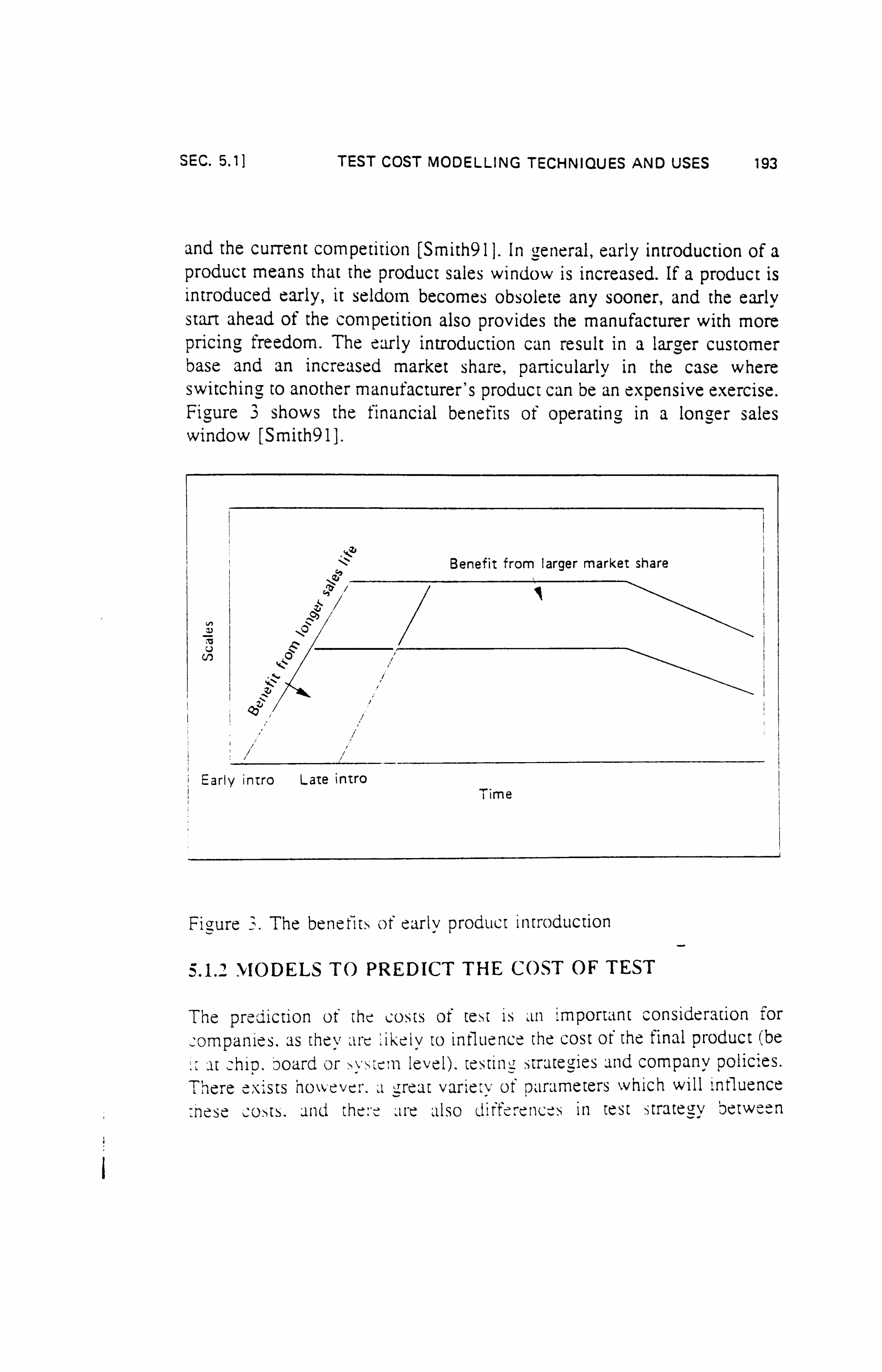
SEC. 5.11 TEST COST MODELLING TECHNIQUES AND USES 193
and the current competition [Smith9l 1. In `(general, early introduction of a product means that the product sales window is increased. If a product is introduced early, it seldom becomes obsolete any sooner, and the early start ahead of the competition also provides the manufacturer with more pricing freedom. The early introduction can result in a larger customer base and an increased market share, particularly in the case where switching to another manufacturer's product can be an expensive exercise. Figure 3 shows the financial benefits of operating in a longer sales window [Smith9l].
N
U
a+y
zi
\a.
.o tiý / m;
ý"
Early intro Late intro Time
Figure 3. The benefits of early product introduction
5.1.2 MODELS TO PREDICT THE COST OF TEST
The prediction of the costs of test is an important consideration for
companies, as they arc iikeiv to influence the cost of the final product (be
at chip. board or ýý sce: n level). testing strategies and company policies. There exists however. a great variety of parameters which will influence
: nose costs. and there are also differences in test strategy between
Benefit from larger market share

194 TEST COST MODELLING [CH. 5
companies. These costs can be modelled, and a number of papers have been published describing the use of economics models for a variety of applications. However, both the scope of the model and the application of it need to be carefully defined.
By far the most common use of test cost modelling is in examining the costs of using automatic test equipment and determining the optimal tester use. Existing models use techniques of various levels of sophistication in order to compare test strategies, evaluate the cost of test application and determine product quality [Taschioglou8l]. In attempting to satisfy these objectives there are several important considerations, such as examining the optimum level of test required by costing the effects of escaped faults at each stage, as well as taking the complexity of the product under test into consideration (Mvers8 I.
Economic models can also be used to examine not only test strategies but also the performance of ATE systems. Most economic analyses performed in order to determine a test strategy in terms of the mix of ATE equipment used, analyze the cost effectiveness of different testers. Another way to look at the problem is to analyze the cost effectiveness of enhancements (in terms of CPU, mass storage. and tester throughput) to a specific tester [HustonWý? ). Other aspects of test can also be examined by the use of cost modelling techniques. The prediction of test pattern generation costs is one particularly difficult problem, and empirical models c. -an be used to approach it, ultimately linking . 1st pattern generation costs to circuit complexity and required fault cove: ; GoeiSO].
Another area of interest where the use or economics models Can prove is in the evaluation of design for test Aspects and costs. This s often done by considering the increased die area and associated product on cgists,
t reduced tester use or the use of a cneape:.: ess which can be offset again, powerful system (Pitmans-', l. There are models mich can be . used to evaluate the area overhe: id : esultin_7 from ror me: nods ([Ohletz8,1, [tililes8; 1)
What : neue techniques iia\e in -omi-non .' -nölt isolated manner. For ;, xampie. ATE u>e may ` adidresjetý from test pattern Tener, lcicýn lind ; rom the ýýi T : or An

SEC. 5.11 TEST COST MODELLING TECHNIQUES AND USES 195
alternative method is to attempt to unify the test cost modelling by considering the whole design. production and test cycle for a system, and the costs associated with improving the testability of the design [Varma84], [Dear881 [Dislis89].
5.1.3 USING ECO\O\IICS MODELLING FOR TEST STRATEGY PLANNING
Economics modelling can be automated for embedding into systems for making decisions on various test aspects. One such system has been developed jointly by SIEMENS and Brunel University and is currently under industrial evaluation [Dislis9l]. It uses global cost modelling methods based on industrial data to aid designers in choosing the optimal mix of structured DFT methods for a particular application at IC level. A knowledge base of DFT methods specific to functional blocks holds
economic and design information. Test decisions can be guided by the user, or be taken b\ a ýeiec tion of automatic test strategy planning algorithms, all based on cost evaluation of alternative strategies. The
technique can be extended to examine many other test related aspects. This work is now been extended to VLSI based systems, in order to create a complete testability advisor. The system was developed with the needs of industry in mind. and there is built in flexibility in the implementation
of the cost model used. as well as the selection of test methods in the knowledge base. Speed of calculation was also an issue, so backtracking
was avoided as much I. possible. A, the system was designed to operate in the early stage,, of the design. it is up to the designer to implement the ; u., vested measures. althouU'il help is provided in the implementation.
5.1.3.1 The Structure of the Test Strategy Planning System.
Figure -4 shows the Ou: line ý)t the : est strategy planning system. The design description iý, UCLluired either directly' from the user or from an existin g nztlist. and is buht in a hierarchical fashion in order to allow test ýtratea' `1C:: 5: ý)I1ý to 'Je 11.: ýC ±t ýý e:. ý! eta es of the design process. A
: 11ýso : ýcauire ., it the same time.

196 TEST COST MODELLING (CH. 5
The data is used to automatically update an economics model prior to the test strategy selection process. The test strategy planner uses stored knowledge on test methods as well as the design data and the existing cost model to evaluate a variety of test strategies. The test strategy control can be left entirely to the user, or alternatively, a degree of automatic planning may be employed to accelerate the selection.
Test strategy planner structure
USER Netlist Cellsize
Design specification reader
Cost ; Design TM- I descriptions
m odel Description ýceII library data
Test planner
Results
Figure 4: System architcc: ure
5.1.3.2 The cost model
The cost model caregorises primary parameters supplied by the user into design independent (mostly global company costings), design dependent (which will change wich the design). test method dependent, and constant factors. A set of equations is then calculated using the supplied values. Design costs are modelled in terms or and equipment required, the cost or using an external dem,
-, ii �trlrre it rhis option is taken, and manpower. '. which is a function or the complexity or the system, and the productivity of the design ýnýircýºrý>>c; ý;. ProdiuctivIt\ modelled in terms of the

SEC. 5.11 TEST COST MODELLING TECHNIQUES AND USES 197
designer's experience, the performance of the CAD system, and the functionality of the cell library.
Production costs for are linked to the design complexity (measured in gate equivalents, grids or mm`), mostly with a linear relationship within certain complexity ranges. In this case, gate equivalent count was used as a complexity measure. A test strategy may influence the gate count and therefore the production cost per unit. In addition, non recurrent engineering (NRE) charges must be added to the production cost. Unlike previous models [Varma84, Dislis89], yield effects are not modelled separately, as they are included in the pricing policy of the vendor.
Test costs are separated into test pattern veneration and test application costs. Test application costs are linked to the number of test patterns in linear or stepwise ranges, similar to the way (Tate count is linked to production cost. This pricing is normally provided by the vendor, and removes the need for the separate modelling of ATE costs present in previous models. Test pattern generation costs are estimated as follows: the cost of automatic test pattern generation is estimated, together with the maximum achievabie : Ault cover. If the achievable fault cover is less than the required value (, a1 t'undamm1ental requirement) then the cost of achieving it using ; , pensi\- manual tpU IS estimated. using structured DFT methods often means that ATPG techniques alone are effective for croducing the required fault cove: ".
5.1.3.4 The test strategy planning process
The user has the : opticonl tco apply and evaluate test methods for specific blocks manually. h, ch allows a 'cat of `lexibility. Ho%vtver, it was necessary to also automa[t this process, and a , lumber of algorithms are supplied with the ,v stem. These work on : he following principles: The first requirement block testable. This means that the block would be easily testable it it %vere tested in isolation. with perfect access to all its üo tine,. On this basis, a \, ost optimal testability method is chosen for ýý .. Dioc. n the ircuit, by t% aiuatin_ all suitable methods for each. At : he --,, u, or :r is rocess. e Cry block Should be testable. but the acL: e ibiiity oI ýý)fllý nLoc; ýý 'lll_r'lt . ilýi` lave !n eased.

198 TEST COST MODELLING [CH. 5
The next requirement is one of accessibility to all i/o lines of every block, in order to be able to propagate the test patterns required. In order to determine where the accessibility problems are situated, the accessibility of i/o line groups is established. This information is used to determine whether any accessibility test methods need to be applied. This may or may not be the case, as many testability enhancing methods have the side effect of improving accessibility as well. There may be several candidates for the application of accessibility methods, and the aim of the algorithm is to find the block which has the maximum impact on the accessibility of the circuit, taking into account existing (already applied) test methods and the transparencies of paths through functional blocks.
----------------------Bus--------- ------s5--i s9 s6ý
'
S10 . i1 S7
RAM 4Kb 01 o2 X16 6 01 o2 : Random logic
block3 bbI blockt rw il cl i3 cl i2 i3
node4 node3 ss
s12 511
16 1ý8 16
PLA o2 of of o2 Random logic blockt b block2 il i2 cl 12 i3
nod-el I-- JnOO82:
i8 8 16
s1 cl s3 s4 -------------------------------------------------
Demo circ
Figure 5. An C. ß; 1I11n1C ,I ui
Figure f shows an c, \ Lnlpie circuit, . lnd ti_L; re 6 shows example costs of the automatic test , trate`7v piannin; procas eac: ý block is tackled. It
should be noted that the production volume is a sensitive parameter. altering the relative , tra1Cgv costs. The test >trate_v results are obviously valid only for : he specific circumstance,,, and the test methods

SEC. 5.1] TEST COST MODELLING TECHNIQUES AND USES 199
([Treuer85], [Illman86], Zhu881) are block specific and their descriptions are part of the system [Dislis9l ].
DFT strategy for example circuit 5000 ICs
700
600
500
400 ° 300 V
N 200 0 v 100
0
n eXt'ýan, Seý
node, ode 'I
Scao ode3,
de4, 'ý\\týa0 O°
roae2, D FT strategy
Design Production ATPG MTPG Test appl.
Figure 6. DFT strate, Tv for ý(X)O IC,
5.1.4 CONCLUSIO\S
This chapter introduced some of the ractors that affect test costs and test decisions, and discussed the way DFT can affect them. Some of the difficulties of test wer; nighli; hted. and the need for a high fault cover was illustrated. The prediction or test related costs is an important
consideration. and aº variety of moc e!; which attempt to analv:. e test costs from different vie'. y points . giere reviewed: one of these specifically for the evaluation of alte: nati\ e broad') DFT methods. Finally, the possibility of usin, economic : echniclueý or detailed decision making on the choice or the optimal c )mbina[ion, )r test methods for a given circuit was discussed. A >ý ß[Cm : ýýr :e "[l-ate', ` t! anniný_ using? economic factors was
then desc gibed. Iý r :eo! IL: ýi.. ItC
he indu trial validity of the
technique.

200 TEST COST MODELLING (CH. 5
The system described leere is still under evaluation, but we believe it is a useful tool for aiding designers in enhancing the testability of their designs. It is easily reconfigurable in terms of the cost modelling and test method description to suit different users. The concept of test strategy planning is now being taken through to test strategy planning for VLSI based systems. based on the principles of economic evaluation and test strategy selection.
5.1.5 REFERENCES
[Abadir89] 'TIGER: Testability Insertion Guidance Expert System'. VI. Abadir, Proc. IEEE International Conference on Computer Aided Design, 1989.
[Browny ll 'The product liability handbook. Prevention, risk, sZurlsegluence and forensics of product failure', Bro\\, n. Sam ! eel), Van Kostrand Reinhold, 1991
IDaniels851 ' Built-In Self-Test Trends in 'Motorola 1v1icroprocessors'. Daniels, R. G.. Bruce, W. C., IEEE Desi_n & T; st of Computers, Vol. 2, No 2,
April i98-5. pp 04-71
[Dear88I -Hierarchical Testability Measurement and Design I'm Test Selection by Cost Prediction', I. D. Dear, C. Dk,, lis. S. C. Liu. J. R. Miles, A. P. Ambler, Pr oceeLIin 7ý or the European Test Conference,
(Dears Hi; rurchicai Testability Measurement and Design
or Te t Seiec.: on b\, Cost Predication', I. D. Dear, C.
Dig i,. S. C. L ILI. J. R. Miles. A. P. Ambier, Proc.
r: ýýupe: ýn Tý., t Conference ly*S .
Deat'9I I i-.;; oriomic E<<:: ý: t, in Design and Test'. I. D. Dear, C. Di,, ii-,.
. A.;?. Arllolcr. J. Dick, IEEE Design and
T: ýt ýýt :. ern gute ý. cri. 7. no. 1991.

SEC. 5.1 1 TEST COST MODELLING TECHNIQUES AND USES 201
[Dislis89! 'Cost Analysis of Test Method Environments', C. Dislis, I. D. Dear, J. R. 'Miles. S. C. Lau, A. P. Ambler, Proc. International Test Conference, 1989.
[Dislis911 'An Economics Based Test Strategy Planner for VLSI Design', C. Dislis, J. Dick, A. P. Ambler, Proceedings of the European Test Conference, 1991.
[Goel80] Goel, P. 'Test Generation Costs Analysis and projections' Proceedings of the IEEE 17th Design Automation Conference, 1980, pp 77-84.
[Huston83 J Huston. R. E. 'An Analysis of ATE Testing Costs' Proceedings of the IEEE International Test Conference, 1983. pp 396-405
[Illman86) 'Design of a Self Testin_ RAM', R. J. Illman, Proc. Silicon Design Conference 1986.
[McCluskey88] *IC Quality and Test Transparency'. McCluskey, \I. J., Proc. IEEE International Test Conference, 1988, pp 295-301
[Miles88] J. R. Miles. PhD Thesis. Brunel Lni%ersity, UK, 1988.
[Mvers8 3 v1yers, M. A. 'An Analysis of the Cost and Quality Impact of LSI/VLSI Technology on PCB Test Strategies' Proceedings of the IEEE International Test Conference. 1983, pp 38 - 95
[Ohletz87 j Ohletz, M. J.. Williams, T. W.. Mucha, J. P. 'Overhead in scan and Self-Testing Designs' Proceedings of the IEEE International Test Conference. 1987. pp 460-410

202 TEST COST MODELLING RCN. 5]
[Pittman841 Pittrnan. J. S.. Bruce. W. C. 'Test Logic Economic Considerations in a Commercial VLSI Chip Environment' Proceedings of the IEEE International Test Conference, 1984, pp 31-39
[Racal-Redac89I Private communication, Racal-Redac, 1989
[Smith9l I 'Developing products in half the time', Smith, P. G., Reinertsen. D. G., Van Nostrand Reinhold, 1991
Taschioglou811 Taschioglou, K. P. 'Applying Quality Curves for Economic Comparisons of Alternative Test Strategies' Proceedings of the IEEE International Test Conference. 1981, pp 3-33-31-33339
[Treuer85 l 'Ilnplementiny, a Built-In-Self-Test PLA Design'. R. "I Celler, H. Fujiwara. V. K. A rawal, IEEE Design
: IiiU fest of Computers. Vol. 2, April 1985.
[Turino901 'Design to Test -A definitive guide for electronic desiVgn, manutaacture, and service', Turino, Jon. Van \ostrand Reinhold. Nerv York, 1990
I VarmaS4I '. An Analysis of the Economics of Self Test', P. Varmu, A. P. Ambler. Proceedings of the IEEE 1I1ici-national Test Conference, 1984.
[Varrna841 ýu Analysis of the EConomicS of Self Test', P.
aril. A. P. Ambler, Prot:. IEEE International Test
- Conference. 1984.
[Zhu8SI 'Analysis of Testable PLA Designs', X. Zhu. M. A. Breuer. IEEE Design and Test. Au(Tust 1988.

EC0N0 , UI ICE .FFACTS
Economic Effects in Design and Test
It can be argued that not enough
information is available about the economics of electronic circuit de- ign, either about specifically design-
related issues or about test issues. However, the information that is avail- able can be illuminating and interest- ing. Davis has written a book about test costs. I Also, Fey and Paraskevo-
poulos have written about the design
costs of integrated circuits. ' 3 Area overhead is often perceived
to be a major factor in test cost in-
crease. Figure 1 provides an example of costs as a function of test-related area overhead. However. certain questions arise from this relation. such as, what level of test area overhead leads to minimum costs?
The available information about the economics of circuit design must be studied carefully because it can- not relate. other than in a very broad
sense, to any one set or crcumstanc- es. The wide range of factors that can affect test costs can vary. - widely rom
, one installation to another and from - one 7esian -o another. However. an eco-
nomic analysis of indiv : cuai pest costs OF
. en points the way to more efficient use of
rest tools and DFl': ecnnicues ano eventu-
ally relates ro improvec-, product quaii-z
when .t !s realized that , oo rest can pay
)ac K. in . his amc! e. we j sc iss various 'esc
Ost ; ssueý We also DrCsent a 'est cost
. D. DEAR
DISLIS A. P. AMBLER
Brunei University
J. DICK
Siemens-ýN dorr
Because of misconceptions and myths about the cost of test, many devices and systems are inadequately tested. Focusing
on application-specific ICs, the authors discuss the economics of test and show how economic analysis leads to test that
pays back. They also present the EVEREST
test strategy planner, a design tool that
aids in the selection of DFT structures during ASIC design, using cost as a primary
selection paromerer.
model that has gee 1sec as a : )uresoread- sheet modei anc :s now 7e: r sz as parr
of a test-strate<_zv manning tool.
Test economics As muht be test.
nothing is done -o ease he probiem. in-
creases faster than ! inearw gor a linear
increase in circuit complexity,. 4 W hile
total product cost has decreased over the past few years. test cost has risen as a percentage of this total product cost to more than 555°,, in some cases. The extent of the increase depends
on the product size. technology, and complexity.
Unfortunately, many myths sur- round test costs. Test pattern genera- tion has not been generaily accepted as a possible answer when observed from the perspectives of fault cover- age and CPU time. Significantly large CPU times for fault simulation are often cited as obstacles to effect, % e test. Though there are a variety of solutions to such difficulties. the so- lutions have not been widely accept- ed. Among the many reasons given for not using such DF i methods as scan and built, n seif-pest are the -a-
miliarproblems or performance: e-- alty. area overhead. anc pin-count overhead.
Because of these misconceptions.
- many devices anc systems are inace-
cuateiv'esred. Si! is^, n": encorssav, h at -1n to -11, at ... vorkin, y appiicat, on-specific ICs , cu not work in the target svstem::: ne
_Jesrgns have not peen soe-c: r: ec or . en-
: iec correctly because or : ac_! k of ; im.: ia-
: ion. ' and : nev nave not been tested ace-
ýuateiv. Desi, Jn e rrican. n tests or devices typically- provide 4! 1-- !"- fault cov-
erage. despite . varn, r. gs 'nat greater than
64 -ý ý'; a' o'= )0645o 'o 99 _-= IEEE DESIGN & TEST OF COMPUTERS

Total costs
Processing n
Packaging
Test
30 Test circuit area overhead (in percent)
Figure 1. Plot showing costs and test- related area overhead.
aß'--, fault coverage is necessary to ensure adequate quality. °
To the uninitiated. publicity showing that the cost of test is rising dramatically
only reinforces the opinion that test is not cost effective. Concern about the real cost of test leads to shortcuts and to a naive
reliance on the results of perhaps ques- iionable test-generation and fault-simula-
: ion methods. Because it is a negative quantity. the
_ost of test is easier to focus on than the benefits. especially when an "over-the-
vall" mentality prevails. as it often does
,. v, nen the design team is asked to use its
esourcesand budgetto improve the lot of : ne test department. To make realistic 'voices. we must understand the prob-
. em of testability in more detail. and in
-erms related to the whole company, not
_st lo individual departments. Let's con- sider scan path use as an exampie in the Hext section.
Scan path testing Scan path test methodoio; \ is weil un-
-ý and we will not expand on t . sere. Scan path use increases observabil- ,,, and controllabiiity. it : -educes the 'lest problem iromsequentiai c rcuit resttotest )t a combinational circuit plus a shift e. seer. Automatic test pattern genera-
'ion capabiiity is available commercially 'or combinational logic. iwing the possi- 11iirv t-)f near-100°, stuck-at fault coverage
and thus a higher quality device under test. Scan can be used at all stages in a system design. from initial design debug- ging and device production test to system test and field service.
However, often-cited penalties of using scan include
additional design effort additional circuitry t 4-20°ö over-
head) additional device pins. sometimes
requiring use of the next package size, which takes up more space and costs more
I possible increase in test-application time
degradation in reliability and yield
An industry survev3 shows that very few ASIC designs incorporate scan. Often-cit-
ed reasons are area overhead: degrada-
tion in performance. reliability, and yield: and the necessity for design constraints. '
Some of the negatives above relate to design philosophy and performance ; s- sues that we do not discuss here. The wide range of software tools and support avaii- able for scan design includes scan design
rule checkers. automatic scan-conversion
350
300
250
200 I, ='50
-' 00
30
J '. J00
tools. and automatic zest pattern genera- tion. The other more directiv cost-related issues require some detailed anaiysis fora true comparison. The factors; nvoived in- clude the following:
The balance between increased gate count and the impact the increased count might have in increased de- sign time. greater processing costs. and decreased %-ieid (ie%. er devices per wafer) and reiiabiiitz-
The balance between easier test pattern generation and higher fault
coverage on the one hand and po- tential increase or decrease in test time ; serial application of tests.
which might be aggravated or eased by the absence or presence of a scan tester) on the other
Such factors can be compared on straight economic grounds for a quantita- tive evaluation of scan as a : est method. The qualitative issues are `or individual design teams to evaiuate.
Nevertheless. the cost of 'est. with or without scan. verv much favors the use of scan. ' as Figure 2 shows. he graph :. ̂. Figure 2 does not take into account the
3. X00 1 0.000 30.000 '. 000
Sates
, onventional test orograrrning -------' _ -Jil scan test --cgrarnrri g
Logic design
Figure 2. Typic--i ASIC engineering costs.
öä DECEMBER 1991

ECONOMICEFFECTS
benefits to the board. system. and field
test stages when the entire design includes the scan design philosophy. Dervisoglu1° demonstrated the benefits of systemwide scan test.
The effectiveness of improved testabili- týv-and hence scan-from the device lev-
el to subsequent test stages is simply put by the "rule of tens. "' This rule holds that leaving test to the later stages of system integration and poor-quality test at the device level lead to very large cost in-
creases in field failures. According to the rule. if detecting a fault at the device level
costs, say, $1, then detecting the same fault at the board level costs 310: at the system level. $100; and in the field, $1,000. Analyses of the real costs based on actual examples show this rule of thumb to be
reasonable. (The figures for testing a de-
sign flaw could follow a similar pattern and be a lot higher. )
Need for economic analysis In addition to the need for a straightfor-
ward economic analysis of the costs of test. consider the dilemma of designers
who need to choose a DFT strategy for
their ASIC. Even for designers completely familiarwith the available test techniques, the choice can be difficult. For example. Zhu and Breuer' I discuss 20 BIST methods or programmable logic arrays. Given that
, esigns can include PLAs and otherstruc- turesaswell. the iistcan become daunting.
'actors that must be considered when , ec. ding on the test method for any de-
siun include. but are not be limited to. area overhead. pin count overhead, test . ength. fault coverage, and automatic test eauiDment requirements. They also in-
, _ude such design-dependent : actors as design time, circuit size, pertormance -mpact. and test pattern generation costs.
The modes we consider here extend to
over 100 parameters, and we cannot dis-
, Jss them in detail. When constructing 3
, iobai economics modei, we sound it nec-
essarv to consider ail these parameters rather than a subset-perhaps including
«niv area overhead. test time. and a few
other parameters-to put any true savings into perspective. There are cases in which a simple subset can be usefully applied. but we have found that the enlarged model is useful in the initial stages to prevent preconceived ideas about the rel- ative importance of the parameters com- ing into play. A fuller discussion of the necessary parameters can be found in the literature. ! 2- 14
All factors vary with circuit style, so we need some procedure to compare and contrast the disparate values to produce a meaningful judgment. When confronted by what could be conflicting issues of longer test time versus larger area over- head versus increased pin count require- ments, how can we reconcile them satis- factorily?
Of course, there are many cases inwhich
the variables listed are not variables. For
example, there may be design constraints such as package size limitations that fix
area overhead or pin count (as in an aero- space design). However, how to effective- ly compare and contrast the effects of all the variables associated with a test strate- gy remains an issue.
arma, Ambler, and Bakeri- showed : he effects of analyzing many different
test-related parameters using cost as the basis for comparison. Graphs of specific cases showed how the relative benefits of BIST versus scan versus no DFT varied
". vith production quantity. In the casesstud- : ed. the changes were quite marked: BIST
was the preferred method for tower pro- duction volumes. and no DFT was best for
higher production volumes. Further studies, ' brought different re-
suits: Higher production quantities in-
. reased the benefits f using `AFT com- pared with not using DFT. Such "vork only emphasizes the requirement for econom- ic analysis of any given design. manufac- 'ure. and test scenario.
. Ve emphasize here. as . ý-e again ater. that because of the variety of issues
considered, any figures we give in this 3n; c'. e relate only to the examples from
,. vnich they arise. The figures will not nec-
essariiv bear any resemblance to figures from comparable examples in other companies.
Different test-related quantities can be
effectively compared using cost as the basis for comparison, allowing for true quantitative comparison. Any other form
of comparison can only be subjective.
Test-related parameters
The effects of adding testability to a design are widespread. To assess the im-
pact of a DFT strategy, we must consider both the direct impact on test costs (such
as test pattern generation) and also such factors as the reduction in ATE complexi- ty and increase in design time and cost. Let's consider the main tangible cost ar- eas affected by test decisions: design, man- ufacture. test generation. and test applica- tion. Note that costs can vary greatly among productsand companies. We offera guide to the possible benefits or penalties of DET.
Area overhead I he area overhead penalty is often cit-
ed as a principal argument against DFT. The argument that DFT increases chip area and decreases yield, hence increas- ing production cost. is well understood. However. no general figure can be set as . he maximum allowable area overhead associated with DFT. Designers are often ! eft to make the best assessment they can. Sometimes a limit is imposed on the de-
sifln 'rom another source. The origins of this', imit are often hard to ascertain, leav-
ing ; nanswered 'he question of wnem, er the cost saving of the area overhead nas been properly considered.
\lcs companies in the iabncation in-
iustr. ; eep a close watch )n the `hip vie! d of their process lines. Depending on
. he - %voe of device produced, the ! ecnnoi-
og and soon. these companies use mod-
eis to calculate the yield of devices, given
66 1911 DESIGN i TEST OF COMPUTEIS

a chip area. Abundant research has been devoted to this yield. Even when designers
ha,, e access to these models. they must calculate closely the area overhead of the
w. vnoie chip before assessing the effect on the yield and the consequent effect on the
production c. )st.
Predictive measures. The effect of DFT methods on circuit area is important.
and designers should be able to predict it
as early as possible. Milestb it developed a method for accurately predicting the area overhead (or macrocells when DFT is
added. The functional area of the macrocell is
determined by parameterizing the floor
plan of a given circuit structure before and after impiementincy a specific test strategy. Thus. designers can determine a parame- terized model for anysize cell. The predic- tion model also includes additional rout- in; area and wasted area due to pitch mismatching when DFT cells are added. Using a probaoiiistic model. Miles" con- sicie: -s the p ssibie effect on Klobai routing area overhead . vhen DFT is added to a pail or all, )[ a device.
figure 3 compares. using the Miles ap- proacn. ber. ý ct-n the overheads fora PL-\
with scan and a PL A ". vith built-in logic- block obser. e! - BILBO' registers applied to inputs and outputs. The results show that she ; e! ativ. e )% erheads decrease as the PLA size increases. which is the ex-
'rem,,.
30
ý., 50
=1Q- 77
t .! J
40 50 50 -0 30
umoer )r oroauct terms Figure J. -rea overhead predictions ; or
scan oarh and 31L3O test circuitry op- oiiec 'o P as r70 inputs, 10 outputs).
31LB 0 overhead 30 " Scan overhead
Simplification of production costs. In some cases. the complexity- of the mod- eling process required can be reduced considerably. Companies commonly have specialist outside agents (silicon vendors manufacture their semicustom chip de- signs. Fora given production volume and package spe. the production cost per unit is usually based on a simple gate- count model.
Of course, the actual costs quoted vary from manufacturer to manufacturer. If a company places many designs and or large production volumes -nrough 'the manufacturer. lower costs per unit can be
expected. Figure 4 shows a typical production
cost curve. The addition of DFT logic could increase the pin count beyond that al- lowed fora particular package type in the vendors production model. Thus the ap- propriate adjustment must be made.
Design time modeling Several factors influencethedesign-time
increase %vith the addition of DFT. Feyi3
and Fey and Paraskevoooulos'' produced an empirical model from studies carried out at Xerox Corporation. The model cal- culated . he efficiency of the design de-
partment based on a set or characteristics
related to the design environment and the design itself. This work mghiighted such , actors as
the designers `amiliar, --. with he design
design originality [vpe of technoiow CAD _oois availabie 'he , are counts effect on he design
-ime
The DFT -ime penaity .s crten singled , ut xs arie tines rime-t-murkier. ; Howe. er.
the ý.; esrim en' ironment : as : ren set gip nýncl)ur, FTanddesi_Tnercareskiileii
:n 'hat area. the Denaities -ire much re- 1uced. ' isoý. time-to-market iepends
not oni% )n design time but aiso on test generation time. DFT meth(-cs may in-
400- 350- 300 -
= 250 - 200 -
-7,150- 100- 50- 0
05 100 200 Thousands or ; a: es
Figure 4. Manufacturing cosr versus gate count.
300
crease the time required for the first de-
sign. but they can reduce the time for test generation to almost zero if automatic test pattern generation tools are used. DFT
methods also reduce the probability of redesigns entailed by untestable designs. Taking this argument to the extreme. he
use of a structured DFT approach can often increase the efficiency of the design
center and reduce the amount of rework required. The effect on design time and test generation time is important. With
modem resign systems, often the test e- partment ;s the bottleneck.
Test pattern generation costs Test pattern generation cost is a nonre-
curring engineering cost. Thus. the smail- er the production '. 'olume. 'he greater -; he effect this cost can have. DFT overhead cost is a constant, reoccurnna cost per system or cevice. This is the main reason for the common observation : hat increas- ing DF" :s more attractive for smaller pro- duction . olumes. '=" The `. aii in produc- tion volumes can be linked to the increase in integration and consequent increased
testing costs=)-but don't forget the alter- native cases: ' referred to ear. ier.
a. lthuuah 'he caic nation accur -, e
-est generanon _ý)sts s ". erv . i-cuit.. t as
always attracted a -ii-on ! eve! )i interest.
Goe! named out one )i the -ir5t . 'etai: ý y
studies of automatic -est :. altern genera-
rioýn. -- Hie predic, e: the -lumber of 'est
ectors rt i against : auit coverage for
. ATPL and snowed how test ienýths gar: ;r associated '. with test , eneration cost. produced an ernpincai modei but its
/ý ,, - --
,,.
DECEMBER 1991 67
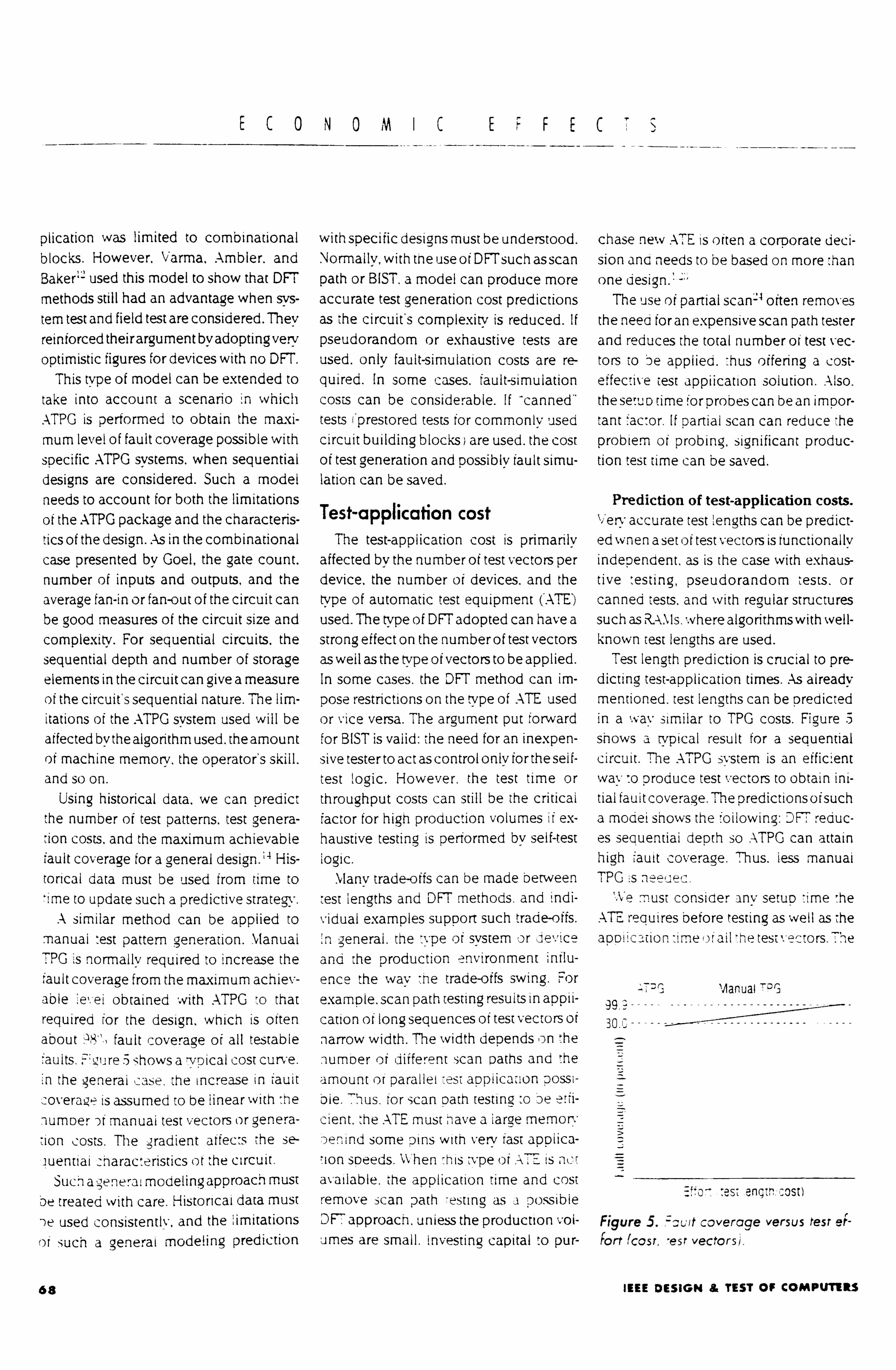
ECONOMICEFFECTS
piication was limited to combinational blocks. However. Varma, Ambler, and Baker' used this model to show that DFT
methods still had an advantage when sys- tem test and field test are considered. They
reinforced theirargument by adopting very optimistic figures for devices with no DFT.
This type of model can be extended to take into account a scenario in which ATPG is performed to obtain the maxi- mum level of fault coverage possible with specific ATPG systems. when sequential designs are considered. Such a model needs to account for both the limitations
of the ATPG package and the characteris- tics of the design. As in the combinational case presented by Goel, the gate count. number of inputs and outputs, and the average fan-in or fan-out of the circuit can be good measures of the circuit size and complexity. For sequential circuits. the sequential depth and number of storage elements in the circuit can give a measure of the circuit's sequential nature. The lim- itations of the ATPG system used will be
affected bythealgorithm used, theamount of machine memory, the operator's skill. and so on.
Using historical data, we can predict the number of test patterns, test genera- tion costs. and the maximum achievable fault coverage for a general design.! ' His- torical data must be used from time to 'i me to update such a predictive strate(gy.
A similar method can be applied to manual test pattern generation. Manual TPG is normally required to increase the fault coverage from the maximum achiev- able ! e'. ei obtained with ATPG o that required (or the design, which is often about ? 8'', fault coverage of all testable faults.: _oure 5 shows a -voical cost curve.
in the ; enerai case. the increase in fault
coverage= is assumed to be linear with : he
TtumDer -)f manual test vectors or genera- tion `osts. The gradient affects the se- iuentiai . haracteristics of the circuit.
Such a; enerai modeling approach must be treated with care. Historical data must
-)e used consistently, and the ; imitations
of such a general modeling prediction
with specific designs must be understood. Normally, with the use of DFTsuch as scan path or BIST. a model can produce more accurate test generation cost predictions as the circuit's complexity is reduced. If
pseudorandom or exhaustive tests are used. only fault-simulation costs are re- quired. In some cases. fault-simulation
costs can be considerable. If -canned" tests ! 'prestored tests for commonly used circuit building blocks) are used. the cost of test generation and possibly fault simu- lation can be saved.
Test-application cost The test-application cost is primarily
affected by the number of test vectors per device. the number of devices. and the type of automatic test equipment (ATE)
used. The type of DFT adopted can have a strong effect on the number of test vectors as weil as the type of vectors to be applied. In some cases. the DFT method can im-
pose restrictions on the type of ATE used or vice versa. The argument put forward for B[ST is valid: the need for an inexpen-
sive testerto act as control only for the seif- test logic. However, the test time or throughput costs can still be the critical factor for high production volumes if ex- haustive testing is performed by self-test logic.
vIanv trade-offs can be made between
test lengths and DFT methods. and indi-
vidual examples support such trade-offs. in general. the type of system or device
and the production environment influ-
ence the way the trade-offs swing. For
example. scan path testing results in appli- cation of long sequences of test vectors of narrow width. The width depends on the
: umber of different scan paths and the
amount or parallei test aopiicanon possi- bie. Thus. for scan oath testing .o ae erfi- cient.. he ATE must have a large memory aenind some Dins with very fast applica- tion speeds. When this type or A, E is nct available. the application time and cost remove scan path resting as a possible DE approach. unless the production voi- umes are small. investing capital to pur-
chase new ATE is often a corporate deci-
sion and needs to be based on more than one design. '-
The use of partial scan=a often removes the need for an expensive scan path tester and reduces the total number or test vec- tors to be applied. : hus offering a cost- effective test application solution. Also. these"uD time torprobescan bean imDor- tant `actor. If partial scan can reduce the problem of probing, significant produc- tion test time can be saved.
Prediction of test-application costs. Very accurate test lengths can be predict- ed wnen a set of test vectors is functionally independent, as is the case with exhaus- tive testing, pseudorandom tests. or canned tests, and with regular structures such as RA`is. ". vhere algorithms with well- known test lengths are used.
Test length prediction is crucial to pre- dicting test-application times. As already mentioned. test lengths can be predicted in a way similar to TPG costs. Figure
shows a typical result for a sequential circuit. The ATPG system is an efficient way o produce test vectors to obtain ini- tial fauitcoverage. The predictions oisuch a model shows the ýoilowing: OF-
reduc-es sequential depth so . -\TPG can attain high fault coverage. Thus. less manual TPG a ýeecec.
'. Ve must consider any setup time the ATE requires before testing as well as the
aoo! cation time, Drail the test. Actors.: he
Manual 'r? I3 09. ------------------------ 30. r------- ----------------- ----
=;: o- . es engmcost
ei- Figure 5. =--uit coverage versus test Fort (cosr, esr vectors,.
68 IEEE DESIGN & TEST OF COMPUTIRS

application of test vectors is not a linear
function of the number cif test vectors. If
all the test vectors can be loaded into the
Din memory. the test-application time is
negligible compared with the load time. If
some test vectors need to be reloaded because the test vector size exceeds the
pin memory size. the additional test-appli-
cation time is steplike. Once the total test time per device has
been calculated. the application cost can be calculated from the hourly rate of run- ning, the ATE and the application speed of the tester. The running cost of the ATE
should include labor and maintenance as veil asthe payback forthe purchase of the
. ATE. The capital repayment will depend
on the initial cost of the ATE and its work- ing '. ife. Thus. different companies may have very different test-application costs for the same devices. =
A practical simplification of test-ap-
plication costs. To obtain an accurate accounting of the test-application costs for a design based on he number of test
%'ectors. we can extend the argument for
rising outside manufacturers of devices from a production cost case to test appii- canon costs.. manufacturer may have
-se' eral different . ATEs. and the one used
ýn-, r : he oarticuiar design can affect the ,t cur e. The customer s bargaining po-
Httoýn will iiso influence : ne cost per unit. Figure 6 shows an example cost curve
As an be seen -rom : he curve. in many cases she manufacturer gives a certain amount of rest vectors ýree and then char;; - -ý-s a ýixe, i cost : >er batcn of 'est vectors. Often this catch size represents she mem-
, au<ýc: t : )f *hN aT ised. or the rea- ;,, ns , ýsc use-: ýarheý.
Overall economic effects of DFT ll? nswl t"; 1,, ion jr ssiles ! scJ sec
in mah n, ' ýoýeý, ýe DFTdeci-
ýný or -xamn, e -i ccm on question cOncems -he maximum ir-ea overhead
ist method. Figure
; hoký> he or i ampie anaivsis of
'hrý: )rohiem. -` e ýýý!. 'S ýlre normalized
with respect to the cost of the unmodified design. The trends are specific :o the de- sign analyzed. and we show -hem here only to illustrate the usefulness of cost modeling. In the economics modeling, we used the simplifications made to the prediction of test-related factors.
Figure 7 is based on a combinational block containing 90 gates. The block oc- cupies 0.001 sq cm of a 0.25-sq cm IC with a production volume of 1.000 ICs.
In this case. when self-test is used. the maximum affordable area overhead be- fore self-test becomes uneconomical is
around 60",,. This is the crossover point. The crossover point forscan is on ly arou nd : 35' ,. This difference decreases with in-
20 - 18 - 16 - 14
12. 10
8-.......
4 -
creasing production quantities (in line
with predictions'') as the costs in the test
generation sector become lesssignificant. We pointed out previously that the over-
all chip size affects the cost effectiveness
of DFT methods for the circuit. because of
reduced yield. However. in the test sector, there are larger savings in a large circuit. The cost effectiveness of DFT then de-
pends not only on the number of devices
produced but also on the size of the de-
vice and the area overhead of DFT meth-
ods contrasted with savings in test costs. To illustrate this point. we evaluated some ASIC designs.
We considered a range of area over- head values for this analysis. The over-
. _. t ýf
32 64 96 128 162 Thousands of test vectors
Figure 6. i est length versus cooiicotion cost per unit.
1.30
1.1 0 ----------------
0.90 -
i. -0
30 50 -') 90
rea )vernead yin 3ercentl
Scan
Figure 7. Cost versus area overhead For different OFT methods, assuming no overhead for no OFT and a production volume of ', 000 ICs.
69 DECEMBER 1991

ECONOMICEFFECTS
head for scan was between 5 and '5 and for . se! f-test between 20% and 30'',. Costs were again normalized to the case without DFT. The difference between the high and low overhead cases widens as the size of the chip is increased, because of reduced vied.
In the case of self-test. the crossover point (the number of chips at which self- test ceases to be cost-effective) increases
as the gate count increases from 5.000 to 10.000 gates and decreases again as the gate count increases to 20.000 and then to : 50.000. The reason is that as the complex- ity of the circuit increases, test generation costs also increase. However, because the chip size increases as well, at one point the increased manufacturing costs be-
come higher than the savings in the test sector. In the case of scan, this effect takes place earlier, as the savings in test costs are not as high as in the case of self-test. Figure S shows; the status fora 10,000-gate. 0.80-sq cm device: Figure 9. for a 50.000-
gate. 2.00-sq cm device. These examples for chip design. pro-
duction. and test only do not take into
account the potential benefits that can be
accrued through reduced board and sys- tem test as a result of improved chip test- abiiity. The benefits to board and system test can be considerable.
EVEREST test strategy planner
Economics modeling can also be used tor more specific DFT, oecision making. as an aid ro designers seeking the optimum mix of DF" methods ýnra oarcicularapoii- cation. Asvstem rorsucn economics mýoo- eling s -he EVEREST test straie(qy oian- : ier. wnich ; ýa. Dracticai implementation
or the BEAST -; v'stem. = BEAST . vas 'e-
ender an Ai%e,. - sc: ieme--, ý\e'. is aL K-sponsored information : ecnnoio- ;y : )roý, lram. I Both eßt strategy planners have aims similar to those of the Tger
svstem. = However, instead of using a
3.0 - ... ....
2.5 -
2.0 - ---. - ------
1.5 - " ----- -- -
0.
15 10 25 50 ' 00 250 -00 ' . 000
Thousands of devices No OF
--- Scan ......... Scan --------- Se! f-yes: 200, o
Figure 8. Normalized cost For a 10,000-gate ASIC. Se; f- es' 3000
14 -
12-
_.............. s
J 1
z ........................................................... .. ------ --- ------------
3 15 10 25 50 1 00 250 500 7z ] 1,000
Thousands of levices
Figure 9. Normalized cost 'or a 50,000-gate -SIC.
weighting system specified 5v the design-
er. both planners use economics model- ing to help the designer make informed DFT decisions. Thus. designers do not need to understand the -elative impor-
tance of all the test-related parameters. The BEASTsvstem was designed to work
in a macrocell ; RAM. ROM. ? LA. and so on! environment. but is modeling was purposely feit as generai as possible. The system successfully showed that , Je-
signers can use economics to select be-
tween test methods. The major problem
No DE --- Scan ......... Scar, ;
Self-es- 200'o S t-'gis: 3O0
with the system was obtain.: 'he cc data to maize it company -nu Procuct specific. The required i esi n. and test pa- rameters ; crexamoie. vie! c ý; nu test aua! - ity are : )b,,. -iousi sen: s: - tive-to the extent that orten : --Dartments within the same comoan% na'. e Drobiemý excnan; insg meanin, ru, owe'. er the svstem --id snow chat -7. r ý-esuits ;. economics-oasen test Dianners are sensitive to different `orr. ýanies man- utacturing and accounting prr ceuuiures. as well as toaifterentteststrate, -,. o äns. "' -
70 IEEE DESIGN & TEST OF COMPUTERS

The natural next step was to integrate a
general-purpose system such as BE. -SST into a company .s CAE environment and
use in-house costing procedures. The
EVEREST test strategy planner addressed
the practical problems of implementing a
usable system. `. Ve carried this work out in
collaboration with siemens-Nixdort as part
of a project sponsored by the European
Strategic Programme for Research in In-
formation Technology. We linked the re-
sulting economics-driven test strategy plan-
ner into the siemens-Nixdorf CAD
environment using accounting informa-
tion generated in-house. ' so obtaining necessary cost data has not been a prob- lem.
Test strategy planning system Figure 10 outlines the test strategy plan-
ning system. The design description can be acquired either from an existing netlist or directly from the user. The description itself is hierarchical to allow test strategy decisions at several stages of the design
process. A variety of essential economic data is also acquired at the same time.
The data automatically updates an eco- nomics model before test strategy selec- tion. The test strate, v planner uses stored knowledge on test methods as well as the design data ano the existing cos, model to
evaiuate a. arier of rest strate, ies. The
test strategy control can either be ; eft en- tirely to the user or automatically planned 'O accelerate The se! ectinn.
Cost modeling techniques The economics model used in EVER-
EST was : -)aseu on previous economics mode! inq work =-': ý but was tailored to the needsoorsemic, istnm cý,. I aesis2n. Tie cost mooe!
--ait, -wr: z s Drimarv Jac3rý--ýers
, ýuppiieJ the -, sei int, ) -hC 'oiiowing : actors: nuenenaent mo,, tIv , lo-
'a lcomoanvaecountin, 3s 7es!, n: 'eýen Cent . vnicn ,. ý ill Lies!, ý- 'est- method depen(ient. constant. The
system hen , vaiuates a yet )T --ýauations ising the supplied values. -ab! e ', gists the
main Darts of the -none!.
Netlist I User I Cell size
Design specification reader
Cost model Design Test method descriptions,
description cell library data
Test planner
Results
Figure 10. EVEREST system architecture.
Table 1. Cost model.
Overall cost
Design Production Test
Engineering
Design complexity Productivity of
design environment Equipment
Design center "Nonrecurring engineering
Production unit ATPG
NRE` charges manual TPG
Test application
Design costs are modeled in terms of design time and equipment required, the
cost of using an external design center if
this option is taken. and manpower. which is a function of the complexity or the system and the productivity of the design
environment. Productivity is modeled in
terms of the designer, experience. CAD
system performance, and coil library func-
tionality. Production costs are linked to the de-
sign complexity (measured in gate equiv-
aients. grids. orsquare millimeters), most- 1v with a linear relationship within certain
_omolexit-, v ranges. n this model. tare
ecuivalent count was used as a compiex- itý- measure. A test strategy may influence
the ; ate count and tneretore the produc-
nion cost aer unit. In addition, nonrecur-
re. ̂. t engineering charges must be added
to the production cost. Unlike in previous
models. ''-: 3 yield effects are not modeled
separately, because they are included in
the vendors pricing policy.
71 DECEMBER 1991

ECONOMICEFFECTS
Test costs are separated into test pattern generation costsand test-application costs. Test-application costs are linked to the number of test patterns in linear or step- wise ranges. similar to the way gate count is linked to production cost. This pricing is normally provided by the vendor and re- moves the need for the separate modeling of .. \TE costs present in previous models. Test pattern generation costs are estimat- ed as follows: The cost of aTPG is estimat- ed. together with the maximum achiev- able fault coverage. If the achievable fault coverage is less than the required value (a fundamental requirement), the cost of achieving it using expensive manual TPG is estimated. Using structured DFT meth- ods often means that ATPG techniques alone are effective for producing the re- quired fault coverage.
The model is coded in a manner that makes it easy for the user to alter. Changes are made in two ways
or text strings. or as equations. The param- eters to be described are categorized in the three groups listed in Table 2.
The first group of parameters is used in the cost model for an economic evalua- tion of the method. The performance com- plexity and the originality parameters are related to design costs. as is the number of extra functions (if any) introduced by the test structures. The pin compatibility in- formation is used in the calculation of the final pin overhead of the plan.
In the design implications group of pa- rameters, the test method type must be specified. At the end of the test strategy planning process. a test strategy must make every block testable on its own) and every block 1/0 line accessible. so test patterns may be propagated to it. This is a requirement of the system. The test meth- ods are therefore categorized as testabili- ty enhancing (internal) or accessibility enhancing (external).
For example. some self-test methods make a block testable but not accessible. Also. methods such as scan path only on
the 1/0 lines provide accessibility but do
not improve the actuai 'esrabiiitv of the block. There is some overiao in this cate- gorization. as some testability-enhancing test methods for example. certain scan options) also provide accessibility to the block. The impact on the accessibility of : he block I/O fines is also stored here. because it is isetul in guiding the test selection aigonthms.
The third group contains the design
requirements of the test method. Fora test method to be applicable to a block, it
must be suited to the type and style of the design and also must fulfill basic require- ments in terms of fault coverage. maxi- mum gate count. and pin count. Data in this section is used to ensure that design
During test strategy planning, the user can examine and alter individ- ual parameters to evaluate their effects.
For more permanent changes ,; for example, to reflect a change in the vendors pricing), the user can sim- ply change the "generic" "or tem- plate') cost model files using a text editor, because the files are stored as text.
Relatively few of the parameters in the model need to be changed from design to design. Those that need changes can eas- iivv : )e obtained from the CAD tool. design.
and test database.
Test method categorization and description
The test , nethoc description , jatabase
7ýeecs to take into account mainly the economic effect of test methods. so that an economic evaluation can be produced. But t shouia aiso assess the suitabiiit-vQi test methods for the particular design. Parameters are described as single values
requirements are met.
Example of test method description The following example shows the coa-
ing of the test method description. The
scan path method enhances the testabili- tv of random seauentiai designs. It does
Table 2. Test method description.
Group
1: Cost model parameters for economic evaluation 2: Design implications 3: Design requirements
Eauivalent gate count Accessibility impact suitable design _icss (PLA, , RA, m)
Seauentiai depth Test method type Suitable designsry le (testcbiiity/ (synchronous, ýlio-
accessibility) Hop design 'ctc- design)
Performance compiexity Additionc: yin courr Originality
Number of extra Functions
Number of test octterns Acriievabie -cult coverage TPG method
J
P'l n compatibility jpossib e shared use or tesr oins)
72 IEEE DESIGN & TEST OF COMPUTERS

not necessarily improve the accessibiiity to the block I/O lines. Table 3 summarizes the information.
When a test method is applied to a block. its design and economic etfects are evaluated. The test method is first checked for compatibility with the design type and style and to ensure that it falls within user- defined limits. If this check is successful. the economic effects are evaluated by
using the test method description param- eters for the cost model, taking into ac- countanycell library support forthe meth- od and also the possibility of testing a number of functional blocks in parallel.
Once the method is applied. its effects on block accessibility are also noted, and the accessibility of other block 1/0 is recal- culated. The recalculation is based on
existing information about transparent "paths" through functional blocks. This
recalculation and the cost model are used to assess the global as well as local impli-
cations of the test method. Testabilittiv- and accessibility-enhancing methods are ap- plied separately. Changes to the design description are not permanent but are current only for the duration of the test strategy planning process. The designer
must implement the test structures sug- gested by the test strategy planner.
Test strategy planning ' he system provides the necessary-
uric-, ions for the .: ser to evaluate a : ariet or 'est strategies and also to use a "7e, ee or
. automated planning. The user can exam- ne the cost implications by examining
the cost model. At the end of the process. _1 test strategy description s produced.
nth details about the test mett,, od ,: nc sen : or ý'. er1 bloc;. ,, t ether with a compiete `ouv of the cost mode! for later rererence. -he design uescrnpnon itself is not aiterec.
Example of test strategy planning
-lie circuit example in Figure 1 on the
Hext _naoe) illustrates the 7iannin! 2 pro-
Table 3. Example of test method description.
Parameter name Parameter value
Test method name Test method type Suitable design classes Seif-test Assures accessibility
Data-in
Control-in
Clock-in
Out
Bus
Performance implication
TPG method
Int_scan
Internal
Random sequential No
No
No
No
No
No
Combinatorial ATPG
Sequential depth
Achievable fault coverage Number of test patterns Overhead formula
Originality impact
Overhead
In-pin
Cur-pin
3i-oin
Pin compatibility class Design style requirements Number of functions
0 Calculated by the cost model Calculated by the cost model 2.5 x gate count of 1 DFF' 1
2
0 1
Synchronous Flip-Flop design
0
`D-type flip-flop
cess. he design description is fuily hierar-
c: micai down to the gate level. out here
only two ieveis of hierarchy are used: the
overall circuit and the circuit subblocks. -` ese are described in terms or `unction-
iR allowing suitable test methods to be
,: nosen'). as weil as connectivity. with at- -rm-; utes to identir<, " control. data. and bus irres. In this case. the blocks are a PLC
^, '1 inputs. ; line outputs, and 50 prou-
; c:: erns: a 4-Kbvte RANt: and two sequen- a:: andom '. ogic blocks of 5.000 gates
each. Information is also given on block
-ransparencv. v.. v; ich allows the system to
derive the accessibility of lines for test
purposes. The objective of automatic lest strategy selection is to ensure that all blocks
are individually testable and that all lines
are accessible. so rest patterns can -e
propagated to the testable blocks. Figure 12 shows the results of the lest
strategy plan at different stages for a Oro- duction volume of 50.000 units. In this
case. four PL-\methods, 1 wereputthrough the cost model. The one chosen was a seLf- test method using cumulative panty com-
parisons. =3 The RAM test methods includ-
ed different implementations of standard
73 DECEMBER 1991

ECONOMIC
A /l
RAM 4 Kbytes Node 4
16
1ý 8
PLA Node 1
"8
Figure 11. Circuit example.
3.700
= 3.600 H
3.500;
3.400 -
3.300--
-200
0.; 3.100 -
(a)
A
I /, 6 ý, 6
1
EFFECTS
A 71
/ý1
Random logic Node 3
' ý16 ýý
Random logic
'ý3 "ý16
Plan 1 Plan 2 Plan 3 Olan 4 Finai
? Ian 1. Node 1: Treuer, 28 node 2: no DFT, node 3: no DFT, node 4: no DFT ?! an 2. Node 1: Treuer, node 2: nt_scan, noae 3: no DFT, node 4: no DFT
an 3. Node 1: Treuer, node 2: nt_scan. node 3: int_scan. node 1: no DFT ?! an 4. Node 1: Treuer, node 2: nt_scan, node 3: int_scan, node 4: 1IIman29 ý! nal. Node 1: Add external scan to node 2 to fuifill accessibility reauirements.
(b)
Figure 12. Test strategy selection for production volume or 50,000 ICs: Results at different stages (a) and plan descriptions (b).
memory test algorithms as well as pseudo- random methods. The method chosen was a pseudorandom method based on linear-feedback shift registers. -9 Internai
scan was used as the most cost-effective .. netnod for making the sequential ran- dom blocks testable. An evaluation of ýccessibility after the inclusion of the test-
abilirv-enhancing methods revealed an
3ccessibilit-vproblem on the group of lines
connecting node' to node 3. An extemai scan path. which is classified as an acces- sibility-enhancing method, modifies --his problem.
The accessibiia-v-method actually incurs a financial penaity, but this is because accessibility improvement is a require- ment of the algorithm and is not directly
accounted for in the cost modei. Cost cai- culationsare made on the assumption that the Dioc cs are fuily accessible gor test pur- poses. The financial penalty of adding an accessibiiir- method is comparativ eiv : ess for larger production volumes. pnnc paily because -he relative importance ýDr extra deveiooment costs decreases wich incre as- ing procuction volume.
If :. e Production volume increases to 250.000.. he plan changes at stage ý .ý. cr. a different test method for the memory ele- ment being chosen. In this instance. a sei - test impiementation of the March algo- rithm proved more cost-effective. This illustrates that the test strategy se; ec: ed :s sensitiv: e to production volume.
We ; gave tested larger circuits n 'ne system. Automatic test strategy planning for a design of '50.000 Pates with six com- binational logic blocks, two RAMs. and one PLA takes 7 to 8 minutes running on an Apollo 4500 workstation. The runtime depends on connectivity complexity rath- er than gate count. The results or 'his circuit snow trends similar to those for the previous circuit. This circuit has peen used to investigate heuristics for pertorming quicker and more effective test strate? v plans.
The E',, 'EREST test strategy, planner .5 current:,; being evaluated at Siernens- Nixcort and is to be used by other coilac- orating companies under the ý`. ERE:
project. t wiil become a commerc: ai --roc- uct . next year.
Related issues A -; traignt economic anaiv is
re! atec -acors can he av serý: i 1n. 1! u 7: : -a,,, ng 'ask. as -. v e i-, a,. e
'. ious : resentations or the mürcra. . a. - ýeeý "eil eceiýec ýv : ni>>e ýrac: ic: r. joo,. 9c _ontirrreo their
Tare e'. -idence of the beneüts " ,r 'C*; a^ naa nor
ýr : use or ; heir perception )i ousts. 7c,.. e,, er. in our opinion ; rne" rat-
tors -ýannor be measured ýc orate .
74 IEEE DESIGN & TEST OF COMPUTERS

enough. if at all. in any economic calcula- tion. Nevertheless. they must be consid- ered along with the measurabie factors.
The effect on the company's image` how consumers and the public perceive its concern with quality-must be a major force in any considerations about a prod- uct testability. For example. If an eco- nomic analysis showed that 0", tauft cov- erage was acceptable on cost grounds. consider the effect on the company image
when that inadequately tested device or system caused the destruction of, say, a civil airliner. Clearly, other factors can tar
outweigh cost considerations! \larketing must also be considered in
any cost-effect analysis. We have not dis-
cussed it here, but considerations of mar- keting are available elsewhere. -0'3' Such factors are important and can greatly at- fect the costs and likely productivity of the finished product, both in terms of defining the original specification and time-to-mar- ket issues.. design change or enhance- ment that results from testability improve-
ments may increase the time required to het a product to market. On the other hang. the product may be delayed in get- ting o market because testability hash been designed in. Some figures suggest that snipping six months iate can lead to a
reduction in potential profits under certain market conditions. - This is in ad Bition to the other negatives of not incor- porating testability!
-, ere is also the issue of whether a mercnant cnip manutac: urer -ias any in- 'erest n Providing improved testability that )enerits the use., or customer. The
economic issues in these cases are nter- esting. How much extra can the customer be . narQed for a new , -es an eatureT
. Accinsg 'estabilirv or the new feature
Increases its expense., An ocnerargumem
is -hat Pusning the bounds of tecnnoiogv %v- en a new device is Deins Designed
precludes the incorporation or testability because testability reduces potential func-
tionai area. Sutwith no testability c: esionec in. now can the customer adequately test its new circuit. '
Not all environments are straightfor. vard enough for economic analysis in the way we describe here. Dear.. Ambier, and ` laun- der, discuss a field service environment in which intangible factors can be quire prominent. An example is the -macho' approach-a field service engineer mere- iv replaces all boards in a s-stem to make it tunction correctly in the shortest DOssi- ble time. without attempting any diagno- sis. This inevitably leads to expensive re- dundant analysis of working boards Deiore they can be returned to stock. Although difficult to quantify. to effects of environ- ment are significant and must be account- ed tor.
Board and system test Although we have not addressed :; i any
detail issues relating to board and system test, there have been significant efforts in this field.
The EVEREST work is now mo\-ng in this direction" and will allow foreconom- : cs-based teststrategv planning at the -, oard and system ! eveis. Previous work that touched on board and system test roes
not appear to go into sufficient retail. Dislis et at. ' showed results that ao some way toward meeting the requirements with an analysis of the potentiai eüecc: s of
boundary scan at the board level see Figure 13ý. They discuss . he issues in-
voived in a : ot more detail than we can here and include further results showing that the benefits of full scan '. ersus bound-
arv scan can reverse with increasing pro- duction quantities. `e% ertheless. econom- ic analyses can be made only wnen comparing like with hike. With a hoard or system designed for boundary scan-so there is no ocher easy way to rest adequate- ly-no comparison can be made. eco- nomicaily or otherwise.
Board and system level analysis will have major implications for. IC test eco- nomics. Some results show that the use of BIST for chip test only is potentially more expensive : ban other methods (again. re- sults depend on complexity. production run. and so on'). But use of these same devices at the board and system levels can dramatically reduce the overall test costs through the -rule of tens" effect), as Fig-
ure 14 on page 76 shows.
Other applications Test is not the oniv area n which eco-
nomic measures aid decision making. The
whole area of design and subsequent man- utacture must not be ignored. The require- ments of concurrent engineering are : er-
1000
0.800-
ýa 7.300 =
rij I -
- J. =00 -
.3 j
goo `lc F $can 3ounaar, scan
3oara -es: 'acKaging
Comoonent test a System test
J ýesýgn ors ýroeuc : ýn
Figure 13. Economic erfec; s or bccrci rest strategies: normaiized cast : cr
systems.
DECEMBER 1991 73

ECONOMICEFFECTS
A
No OFT
y O
U
With DFT
Production volume Figure 14. Cost comparison of possible board test strategies.
tile grounds for extending the methods we described. As with the test analysis, we can visit, revisit. and evaluate new tech- nologies. new design techniques, new manufacturing methods. and old discard- ed ones. We are currently doing such work. Not only will we try to predict the final cost: we will also evaluate the poten- tial means for comparing quantitatively disparate values.
We have presented some economic is-
sues that relate to test decisions made during the design cycle. Our discussion focused on ASICs. and we have not ad- dressed the wider issues of board and system test that are just as important-if not more important-to the overall eco- nomic picture.
We have shown that economic data
can be very valuable in decision making at the design level and that the data can be
used in an industrial environment. In its
present form, the economics model in the EVEREST test strategy planner requires a ! ot of data and some setup time. In the collaborative programs that we have been
working in. these potential drawbacks have not been sufficient to prevent our industrial partners from doing what is re- quired-the benefits achieved can be
large. The economics model needs to be much
simpler to make the EVEREST test strategy
planner marketable for widespread com-
mercial use. To this end. we are conduct- ing a sensitivity analysis to create a re- duced data set sufficient to achieve rea- sonable results. and also to indicate the bounds underwhich the reduced data set would be valid. However, the complete EVEREST model would be available to those who prefer it.
Economics models are obviously use- ful. but they can be difficult to create: Now do we verify a models completeness and accuracy? An effective database requires efficient management. but comparative evaluation can be used effectively. Such
an approach is equally applicable to oth- er design-related areas in which decisions
need to be made. How easy it is to adapt the approach must be reconsidered in
each individual case. Other approaches to testability can and
are being extended to board. system. and field test. Information about the financial impact of field test could be fed back to the designers to allow them to consider alternative and improved test features. Even better. predictive tools that look for-
ward to likely field failures could provide data for use at initial design time. eliminat- ing the need for rework some time after product release.
We emphasize once again that the re- sults shown here apply to specific cases and cannot be considered generally ap- plicable in terms of the absolute numbers shown, breakpoint positions. or even broad trends. The design environment, technology choice. equipment. and geo-
graphic location affect the data used in
any model. The model itself is not sacro- sanct either.
The detailed model needs to be tine-
tuned to each individual location and requirement. not only because of techni-
cal differences but also because of differ- ing accounting procedures. Nevertheless.
a model can be used as the basis from
which to build a more specific example. and this has been done easily and suc- cessfuily in a number of cases.
Ultimately, the argument that test is ex- pensive results in a false economy. Eo
Acknowledgments We thank he United Kin<dom They Dir
, orate. the European Economic C: ommur ESPRIT Directorate. and Siernens-\ixdorr their generous financial support of this wo t
References 1. B. Davis. The Economics of . 4utnmi.
Testing. McGraw-Hill. New York. 19ý-' 2. C. Fey and D. Paraskevo, oouios. E.
nomic Aspects of Technology Selec-: Level of Integration. Design Proauctiv : and Development Schedules. ' in '. .. Handbook. J. Di Giacomo. cd.. \IcGr Hill. 1988. pp. 25.3-25.26.
: 3. C. Fey and D. Paraskevopoulos. -=: nomic Aspects of Tecr nology Selectic Costs and Risks. ' in VLSI Handbook. J. Giacomo. ed.. McGraw-Hill. 1988. pp. 26.20.
4. J. Turino. Design to Test. second ed..,. Nostrand Reinhold. New York. 1990.
. 3. J. Huber and fit. Rosneck. Successiul. 4S Design the First Time Through. Van N. trand Reinhold, 1991.
6. E. McCluskey and F. Buelow. -IC Qua'. and Test Transparency, ' Proc. IEEE r Test Conf., IEEE Computer Society Prei Los Alamitos. Calif.. 1988. pp. 295-30'.
". \l.. Abramovici. M. Breuer. and A. Fri, man. Digital Systems Testing and Testa Design. Computer Science Press. Roy ville. old.. 1990.
3.1. Dear. '_a Test Strategy Planning Mere ology Driven by Economic Paramete' PhD thesis. Brunel University. Uxbric= UK. 1991.
9. B. Wilkins. Testing Digital Circ: iits. Introduction. Van Nostrand Reinhoid.: °-
10. B. Dervisoglu. 'Using Scan Tec-inol,,. for Debug and Diagnostics in a `. Vor t: rion Environment. ' P"oc. IEEE ! nt7 7 Conf.. IEEE CS Press. 1988.
11. X. Zhu and M. Breuer. 'Analvsis -m -- able PLA Designs. ' IEEE Design ; e. s. Computers. Vol.... No. 4. Aug. 14-23.
12. P. Varma. A.. amwer. ina <. 3a 1Cr.
. Analysis of the Economics or Proc. IEEE/nt'l Test Conr:. i ̀ rte. gyp. 2; -
13. C. Dislis et aL. "Cost Analysis or -=st \I- )(1 ý'mironments. - Proc. EE- Conr:. 1989. pp. -3
1. ,. Distis. J. Dick. and A. Economics Based Test Strategy ? lane or VLSI Design. Proc. Second Test Cunt.. VUt-ý erjag. Benin. . 1,1. - 13; -446.
I5.. A. Ambler -c al.. 'Economic3; ly Autonmatic Insertion , )f
76 IEEE DESIGN & TEST OF COMPIJTi
for Custom VLSI, - Proc. IEEE Intl Test D. Reinertsen, 'Whodunit. ' The Search Coit 1986, pp-232-243, or -he New-Product Killers. " Electronic
i6. J. \Iiles.. A. Ambler. and K. Totton. Area and Pertormance Estimation of Design for Test Methods. - Proc. IEEE Intl Coni. Cumouter Design, 1988.
17. J. Miles. Cost Modelling for VLSI Circuit Conversion to Aid Testability. doctoral dissertation. Brunel Univ.. Uxbridge. UK, 19S$.
18. C. Fey. -Custom LSIN1Sl Chip Design Productivity. ' IEEEJ. Soird State Circuits, Vol. SC-20. No. '.. Apr. 1985. pp. 335-561.
19. C. Fey and D. Paraskevopoulos. -. A Tech- no-Economic. ssessment of Application- Specific Integrated Circuits Current and Future Trends, " Proc. IEEE. Vol. 75, No. 6, June 1987, pp. 829-841.
20. J. Di Giacomo. ed.. VLSI Handbook, McGraw-Hill. 1988.
21.1. Dear and A. Ambler. -Predicting Cost and Quality Improvements as a Result of Test Strategy Planning, " Proc. IFIP Work- shop on Fast Prototvping, IFIP. Geneva. 1987.
22. P. Goei, 'Test Generation Costs Analysis and Projections, " Proc. IT th Design Auto- mation Conf., 1980. pp. 77-84.
23. R. E. Huston. "An Analysis of ATE Testing Costs. " Proc. IEEE Int'! Test Cont.. 1983, pp.. 396-411.
24. K. Cheng and V. Agrawal. 'A Partial Scan Method forSequential Circuits with Feed- back. " IEEE Trans. Computers, Vol.: 39. No. 4, Apr. 1990. pp. 544-548.
_5. I. Dear et al., "Hierarchical Testability Measurement and Design for Test Selec- tion by Cost Prediction. " Proc. IEEEEuro- pean Test Conl., 1989. pp. 50,5 7.
26. C. Dislis et al., -Cost Effective Test Strate- gy Selection, " Proc. IFIP Workshop on Knowledge Based Systems for Test and Diagnosis, IFIP, Geneva. 1988.
27. M.. Abadir. TIGER: Testability Insertion Guidance Expert system. ' Proc. IEEEInt'! i; onr Computer Aided Design. IEEE CS Press. 1989, pp. 5562-565.
'S. R. Treuer. H. Fujiwara. and V. Agrawal, 'Implementing a Built-In-Self-Test PL. \ Design. ' IEEE Design & Test of Comput- ers. Vol. 2. No. 2. Apr. 1985. pp. 37-48.
29. R. lllman. "Design of a Self-Testing RAM. " Proc. Silicon Design Cont.. Electronic Design Automation Pulications Ltd.. Lon- don. 1986, pp. 439-446.
J. 'Miles. R. De Bonfit. and L. Daeman. -A Test Economics Model and Cost Benefits
. \nakvsisot Boundary Scan. ' Proc. Second
. urrýoeon Test ! onr . Vde-Verlag, Berlin.
1991.; )D. _S- 4.
: l. M. Levitt and J.. Abranam. 'The Econom- ics . )t Scan Design. - Proc. IEEE Intl Test Cont.. i989. pp. S69-S I.
6usiress. vol. l I. juiy ly2SJ. pp. lUb-m).
;: ý... Dear.. A. Ambler. and C. Maunder, The Application of Analvticai Cost Models for ýn(imisation of Field Service Strategies. '
Proc. ACS/ Intl Workshop Economics or Desi2n and Test. ACM. New York, 1991.
)-l. i. Dick. E. Trischler. and A. Ambler. -DOW: A Defect Occurrence Model for Evaluat- ing The Life-Cycle Costs of Test Strate- gies. ' Proc.. 4C1 Int'l Workshop Econom- , cs _)r
Design and Test. ACMI. 1991.
I. D. Dear is a lecturer in digital systems in the Department of Electrical and Electronic Engi-
neering at Brunel University. His current re- search interests include design and test eco- nomics. rest strategy planning, and CAD for VLSI , jevices. Dear holds a PhD from Brunel ! niversity in test strategy planning and eco- nomic modeling, a BSc in electronic engi- neering from the University of Sussex. and an MR n digital systems from Brunel.
Chrvssa Dislis is a research assistant in the same iepartment at Brunel University. She
currently works on an ESPRIT-funded project
o)n cost-based test strategy planning for VLSI je% ices. hier interests include design for test- Jollity _AD for VLSI devices. and the eco- nomics )t test at chip and board levels. Disiis
, oiý-; s i BSc in electronic engineering from
-ne Lniversitv of Sussex. She is a member of -ne ; EEE and an associate member of the Institute ')t Electrical Engineers in the UK.
A. P. Ambler holds the Racal Redac Chair in
test technology at Brune! Lniversity. He also serves as European representative editor to l£EEDesign & Test ofComouters and recently joined the editorial board of JETTA. He has helped organize several conferences includ- ing ICCD.. EDAC. the International Workshop
on Expert Systems in Test and Diagnosis, and the First International Workshop on the Eco-
nomics of Design and Test. His research inter-
ests include design for testability, the eco- nomics or test. CAD for V ISI devices, fault
simulation. and hardware accelerators. Am- bler holds a PhD in test and simulation of multiple-valued logic. He is a member of the IEEE Computer Society, the ACM, and the IEE. He is a chartered engineer.
Jochen Dick is a staff member of Siemens-
Nixdori's CAE software deg: eiopment labora-
tories. His work includes research in automat- ic test pattern generation and the development
of a DFI' rule checker. His recent research
activities have focused on test economics
and test strategy planning. He holds a MS in
electrical gineering from the Technical Uni-
versirv Di 'Munich.
Direc: iuestions about : his aruc'e to A. P.
. -umbier. 3runel University. Department of Elec: ncai Engineering& Electronics. Uxbridge. Middlesex. '-'B83PH. United Kingdom.
DECEMBER 1991 77

for Custom VLSI. " Proc. IEEE Intl Test 1D. Seinertsen, -Whodunit? The Search ont. 19£36. pp. '? 32-243. or -. ne New-Product millers. " Electronic
16. J. Miles. A. Ambler. and K. Totton. '. Area and Pertormance Estimation of Design for Test Methods. - Proc. IEEE Intl Coni. CumDuter Design. 1988.
17, J. Miles. Cost Modelling for VLSI Circuit Conversion to Aid Testability. doctoral dissertation. Brunel Univ.. Uxbridge. UK. 988. 1
Lýusiness. voi. < <. jury tyus. pp. iuo-iuy.
18. C. Fey. "Custom [Sl/VLSI Chip Design Prod uctivi iv. ' TEEEJ. Solid State Circuits. Vol. SC-20. No. 2. Apr. 1985. pp.. 555-561.
19. C. Fey and D. Paraskevopoulos. -ATech- no-EconomicAssessment of Application- Specific Integrated Circuits Current and Future Trends. " Proc. IEEE. Vol. 75. No. 6, June 1987, pp. 829-841.
20. J. Di Giacomo. ed.. VLSI Handbook, McGraw-Hill. 1988.
21.1. Dear and A. Ambler, -Predicting Cost and Quality Improvements as a Result of Test Strategy Planning. " Proc. IFIP Work- shop on Fast Protottiping, IFIP. Geneva, 1987.
221. P. Goel. "Test Generation Costs Analysis and Projections. " Proc. 17th Design Auto- mation (: onl., 1980. pp. 77-84.
23. R. E. Huston. "An Analysis of ATE Testing Costs. " Proc. IEEE int'l Test Coni.. 1983. pp. 396-111.
24. K. Cheng and V. Agrawal. -A Partial Scan
. Method forSequential Circuits with Feed- back. ' IEEE Trans. Computers. Vol. 39. No. 4. Apr. 1990. pp. 344-348.
3. I. Dear et al.. "Hierarchical Testability Measurement and Design for Test Selec- tion by Cost Prediction. ' Proc. IEEEEuro- pean Test Conl. 1989. pp. 50-: )7.
26. C. Dislis et al.. -Cost Effective Test Strate- gy Selection. " Proc. IFIP Workshop on Knowledge Based Svstems for Test and Diagnosis. I F1 P. Geneva. 1988.
27. M.. Abadir. "TIGER: Testability Insertion Guidance Expert System. ' Proc. IEEEInt I Conr Computer Aided Design. IEEE CS Press. 1989, pp. 562-365.
28. R. Treuer. H. Fujiwara, and V. Agrawal, 'Implementing a Built-In-Self-Test PL. A Design, ' IEEE Design & Test of Comput- ers. Vol. 2. No. 2. Apr. 1985. pp. 3 748.
29. R. fllman. "Design or a Self-Testing RAM. " Proc. Silicon Design Cool. Electronic Design Automation Pulications Ltd.. Lon- don. 1986. pp. 339-k46.
$0. J. \liles. R. De Bonur. and L. Daeman. A Test Economics
. \lodel and Cost Benefits
: \naivsis of Boundar. ' Scan. " Proc. Second European Test Conr_ Vde-V erlag, Berlin. 1u91.: )D
I. M. Levitt and J. Abranam. 'The Econom- ics or Scan Design. - `roc. IEEE Int'l Test Cunr.. 1989. pp. S69-. ti7 t.
':. . Dear. A. Ambler. and C. 'launder. The
Application of Analytical Cost Models for
_)otimisation of Field Service Strategies. ' Proc.. 4C. '! Intl Workshop Economics of Design and Test.. ACM1. New York, 1991.
ý'4. i. Dick. E. Trischler. and A. Ambler. -DOM: Defect Occurrence Model for Evaluat-
ing . he Life-Cycle Costs of Test Strate-
mies. L ? roc.. -'ClM Intl Workshop Econom- , cs -)r Design and Test. ACM. 1991.
I. D. Dear is a lecturer in digital systems in the Department of Electrical and Electronic Engi-
neering at Brunel University. His current re- search interests include design and test eco- nomics. rest strategy planning, and CAD for VLSI devices. Dear holds a PhD from Brunel Lniversity in test strategy planning and eco- nomic modeling, a BSc in electronic engi- neering from the University of Sussex. and an \1Sc in digital systems from Brunel.
Chrvssa Dislis is a research assistant in the
same Jepartment at Brunel University. She
currently works on an ESPRIT-funded project
rn cost-based test strategy planning for VLSI
deices. Her interests include design for test-
1DiiitV' 'AD for VLSI devices, and the eco-
; iomics )t test at chip and board levels. Disiis
:; oiLýs i BSc in electronic engineering from
-ne : niversity of Sussex. She is a member of
-ne EEE and an associate member of the Institute >f Electrical Engineers in the UK.
A. P. Ambler holds the Racal Redac Chair in
test technology at Brunel Jniversiry. He also serves as European representative editor to /E EDestgn & Test orComouters and recently joined the editorial board of JETTA. He has helped organize several conferences includ- ing ICCD. EDAC. the International Workshop
on Expert Systems in Test and Diagnosis, and the First International Workshop on the Eco-
nomics of Design and Test. His research inter-
ests include design for testability, the eco- nomics of test. CAD for VLSI devices, fault
simulation. and hardware accelerators. Am- bler holds a PhD in test and simulation of multiple-valued logic. He is a member of the IEEE Computer Society, the ACM, and the IEE. He is a chartered engineer.
Jochen Dick is a staff member or Siemens-
Nixdorfs C. \E software deveiopment labora-
tories. His work includes research in automat- ic test pattern generation and the development
of a DFT rule checker. His recent research
activities have focused on test economics
and test strategy planning. He holds a MS in
eiectncal>-igineering from theTechnical Uni-
versir. )r `. lunicn.
Direc:: uestions about : nis article to A. P. Amoier. Brunei Universit<. Department of Electncai Engineering& Electronics. Uxbridge. . Middlesex. : 38 3PH. United Kingdom.
DECEMBER 1991 77
Related Documents