Copyright © 2006, PCI-SIG, All Rights Reserved 1 PCI-SIG Developers Conference Europe 2006

Welcome message from author
This document is posted to help you gain knowledge. Please leave a comment to let me know what you think about it! Share it to your friends and learn new things together.
Transcript

Copyright © 2006, PCI-SIG, All Rights Reserved 1PCI-SIG Developers Conference Europe 2006
Copyright © 2006, PCI-SIG, All Rights Reserved 2
PCI-SIG®
Architecture OverviewPCI-SIG®
Architecture OverviewRichard Solomon
IC Design EngineerLSI Logic
Richard SolomonIC Design Engineer
LSI Logic

Copyright © 2006, PCI-SIG, All Rights Reserved 3PCI-SIG Developers Conference Europe 2006
What’s all this PCI stuff anyway?What’s all this PCI stuff anyway?
Presentation will cover basic concepts and their evolution from PCI through PCI-X® to PCI Express®
Specs written assuming designers have these key background conceptsHigh level overview of PCI, PCI-X, PCI Express
Day 1 will progress through:PCI Express Protocols……PCI Express 2.0 5GT/sec Electricals……and will close with exciting new work happening in the area of I/O Virtualization
Day 2 devoted to members like you sharing their experiences implementing PCI-SIG Technologies
Copyright © 2006, PCI-SIG, All Rights Reserved 4PCI-SIG Developers Conference Europe 2006
PCI BackgroundPCI Background

Copyright © 2006, PCI-SIG, All Rights Reserved 5PCI-SIG Developers Conference Europe 2006
Revolutionary AND EvolutionaryRevolutionary AND EvolutionaryPCI
Revolutionary– Plug and Play jumperless configuration (BARs)– Unprecedented bandwidth
• 32-bit / 33MHz – 133MB/sec• 64-bit / 66MHz – 533MB/sec
– Designed from day 1 for bus-mastering adapters
Evolutionary– System BIOS maps devices then operating systems boot
and run without further knowledge of PCI– PCI-aware O/S could gain improved functionality
Copyright © 2006, PCI-SIG, All Rights Reserved 6PCI-SIG Developers Conference Europe 2006
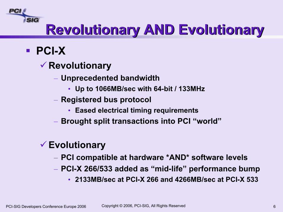
Revolutionary AND EvolutionaryRevolutionary AND EvolutionaryPCI-X
Revolutionary– Unprecedented bandwidth
• Up to 1066MB/sec with 64-bit / 133MHz– Registered bus protocol
• Eased electrical timing requirements– Brought split transactions into PCI “world”
Evolutionary– PCI compatible at hardware *AND* software levels– PCI-X 266/533 added as “mid-life” performance bump
• 2133MB/sec at PCI-X 266 and 4266MB/sec at PCI-X 533

Copyright © 2006, PCI-SIG, All Rights Reserved 7PCI-SIG Developers Conference Europe 2006
Revolutionary AND EvolutionaryRevolutionary AND EvolutionaryPCI Express (aka PCIe)
Revolutionary– Unprecedented bandwidth
• x1: 250MB/sec in *EACH* direction• x16: 4000MB/sec in *EACH* direction
– “Relaxed” electricals due to serial bus architecture• Point-to-point, low voltage, dual simplex with embedded clocking
Evolutionary– PCI compatible at software level
• Configuration space• Power Management• Of course, PCIe-aware O/S can get more functionality
– Transaction layer familiar to PCI/PCI-X designers– System topology matches PCI/PCI-X

Copyright © 2006, PCI-SIG, All Rights Reserved 8PCI-SIG Developers Conference Europe 2006
PCI ConceptsPCI Concepts
Copyright © 2006, PCI-SIG, All Rights Reserved 9PCI-SIG Developers Conference Europe 2006
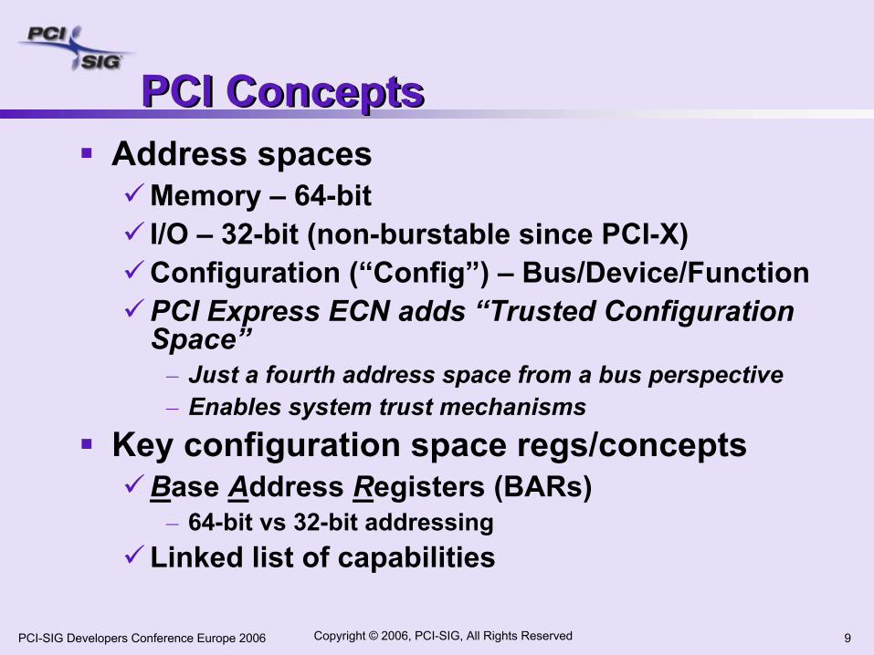
PCI ConceptsPCI ConceptsAddress spaces
Memory – 64-bitI/O – 32-bit (non-burstable since PCI-X)Configuration (“Config”) – Bus/Device/FunctionPCI Express ECN adds “Trusted Configuration Space”
– Just a fourth address space from a bus perspective– Enables system trust mechanisms
Key configuration space regs/conceptsBase Address Registers (BARs)
– 64-bit vs 32-bit addressingLinked list of capabilities

Copyright © 2006, PCI-SIG, All Rights Reserved 10PCI-SIG Developers Conference Europe 2006
Address spaces – Memory & I/OAddress spaces – Memory & I/OMemory space mapped cleanly to CPU semantics
32-bits of address space initially64-bits introduced via Dual-Address Cycles (DAC)
– Extra clock of address time on PCI/PCI-X– 4DWORD header in PCI Express
BurstableI/O space mapped cleanly to CPU semantics
32-bits of address space– Actually much larger than CPUs of the time
Non-burstable– Most PCI implementations didn’t support– PCI-X codified– Carries forward to PCI Express
Copyright © 2006, PCI-SIG, All Rights Reserved 11PCI-SIG Developers Conference Europe 2006
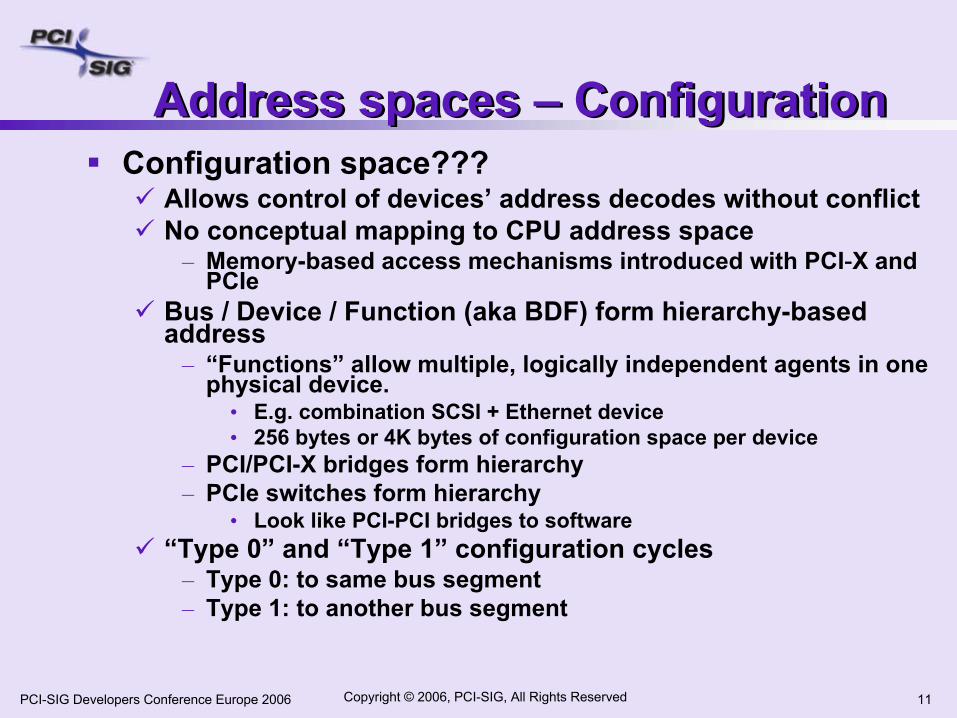
Address spaces – ConfigurationAddress spaces – ConfigurationConfiguration space???
Allows control of devices’ address decodes without conflictNo conceptual mapping to CPU address space
– Memory-based access mechanisms introduced with PCI-X and PCIe
Bus / Device / Function (aka BDF) form hierarchy-based address
– “Functions” allow multiple, logically independent agents in one physical device.
• E.g. combination SCSI + Ethernet device• 256 bytes or 4K bytes of configuration space per device
– PCI/PCI-X bridges form hierarchy– PCIe switches form hierarchy
• Look like PCI-PCI bridges to software“Type 0” and “Type 1” configuration cycles
– Type 0: to same bus segment– Type 1: to another bus segment

Copyright © 2006, PCI-SIG, All Rights Reserved 12PCI-SIG Developers Conference Europe 2006
Configuration Space (cont’d)Configuration Space (cont’d)Processor ProcessorProcessorProcessor
Host/PCI BridgeBus = 0
Subord = 3
Host/PCI BridgeBus = 4
Subord = 5
MainMemory
PCI Bus 0
PCI Bus 1
PCI Bus 2
PCI Bus 4
PCI Bus 5
PCI-to-PCIBridge
Primary = 0Secondary = 1
Subord = 3
PCI-to-PCIBridge
Primary = 4Secondary = 5
Subord = 5
PCI-to-PCIBridge
Primary = 1Secondary = 2
Subord = 2
PCI Bus 3
PCI-to-PCIBridge
Primary = 1Secondary = 3
Subord = 3
Address Port Data Port Address Port Data Port
Copyright © 2006, PCI-SIG, All Rights Reserved 13PCI-SIG Developers Conference Europe 2006
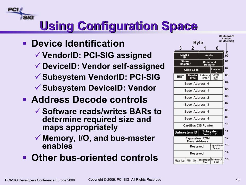
Using Configuration SpaceUsing Configuration Space
Reserved
Reserved
HeaderType
Expansion ROMBase Address
Base Address 5
Base Address 0
Base Address 1
Base Address 2
Base Address 3
Base Address 4
VendorID
DeviceID
LatencyTimer
00
01
02
03
04
05
06
07
08
09
10
11
12
13
14
15
RevisionID
Class Code
InterruptLine
InterruptPinMin_GntMax_Lat
BIST CacheLineSize
StatusRegister Command
Register
DoublewordNumber
(in decimal)
0123Byte
Subsystem ID SubsystemVendor ID
CardBus CIS Pointer
CapabilitiesPointer
Device IdentificationVendorID: PCI-SIG assignedDeviceID: Vendor self-assignedSubsystem VendorID: PCI-SIGSubsystem DeviceID: Vendor
Address Decode controlsSoftware reads/writes BARs to determine required size and maps appropriatelyMemory, I/O, and bus-master enables
Other bus-oriented controls

Copyright © 2006, PCI-SIG, All Rights Reserved 14PCI-SIG Developers Conference Europe 2006
Memory BARs
Note upper DWORD not present when 64-bit decode is not set
Using Configuration SpaceUsing Configuration Space
PrefetchableType
00 - 32-bit decoder. Locate anywhere in lower 4GB01 - locate below 1MB 10 - 64-bit decoder. Locate anywhere in 2 memory space (implies this register is 64-bits wide and consumes next dword of config space as well as this one).11 - reserved
(reserved in 2.2 spec)64
Memory space indicator
0
0
123431
Lower part of Base Address
3263
Upper 32 bits of Base Address

Copyright © 2006, PCI-SIG, All Rights Reserved 15PCI-SIG Developers Conference Europe 2006
I/O BARs look similar to MemoryBit 0 is “1” to indicate I/ONo upper DWORDNo other encoded bits
Using Configuration SpaceUsing Configuration Space
01231Base Address
ReservedI/O Space Indicator

Copyright © 2006, PCI-SIG, All Rights Reserved 16PCI-SIG Developers Conference Europe 2006
Command Register (common fields)
Using Configuration SpaceUsing Configuration Space
Reserved
15 0123456789
SERR# Enable
Parity Error Response
Bus Master Enable
Memory Space Enable
IO Space Enable
1011
Interrupt Disable

Copyright © 2006, PCI-SIG, All Rights Reserved 17PCI-SIG Developers Conference Europe 2006
Status Register (common fields)
Using Configuration SpaceUsing Configuration Space
08 715 14 13 12 1110 9
Signalled Target-AbortReceived Target-AbortReceived Master-AbortSignalled System ErrorDetected Parity Error
Reserved
Master Data Parity Error
6 5 4
Capabilities List
3

Copyright © 2006, PCI-SIG, All Rights Reserved 18PCI-SIG Developers Conference Europe 2006
Using Configuration Space –Capabilities ListUsing Configuration Space –Capabilities List
Reserved
Reserved
HeaderType
Expansion ROMBase Address
Base Address 5
Base Address 0
Base Address 1
Base Address 2
Base Address 3
Base Address 4
VendorID
DeviceID
LatencyTimer
00
01
02
03
04
05
06
07
08
09
10
11
12
13
14
15
RevisionID
Class Code
InterruptLine
InterruptPinMin_GntMax_Lat
BIST CacheLineSize
StatusRegister Command
Register
DoublewordNumber
(in decimal)
0123Byte
Subsystem ID SubsystemVendor ID
CardBus CIS Pointer
CapabilitiesPointer
Capabilities List “Head”
Bit 4

Copyright © 2006, PCI-SIG, All Rights Reserved 19PCI-SIG Developers Conference Europe 2006
Using Configuration Space –Capabilities List (cont’d)Using Configuration Space –Capabilities List (cont’d)
Linked listFollow the list! Cannot assume fixed location of any given feature in any given deviceFeatures defined in their related specs:
– PCI-X– PCIe– PCI Power Management– Etc…
Capability IDPointer to
Next CapabilityFeature-specificConfiguration Registers
0781531 16
Dword nDword 1Dword 0

Copyright © 2006, PCI-SIG, All Rights Reserved 20PCI-SIG Developers Conference Europe 2006
Using Configuration Space –Extended Capabilities ListUsing Configuration Space –Extended Capabilities List
PCI Express onlyLinked list
Follow the list! Cannot assume fixed location of any given feature in any given deviceFirst entry in list is *always* at 100hFeatures defined in PCI Express specification
Capability IDPointer to Next
Capability
Feature-specific Configuration Registers
0781531 16
Dword nDword 1Dword 0
1920Version
Copyright © 2006, PCI-SIG, All Rights Reserved 21PCI-SIG Developers Conference Europe 2006
What is “Trusted” Configuration Space?What is “Trusted” Configuration Space?
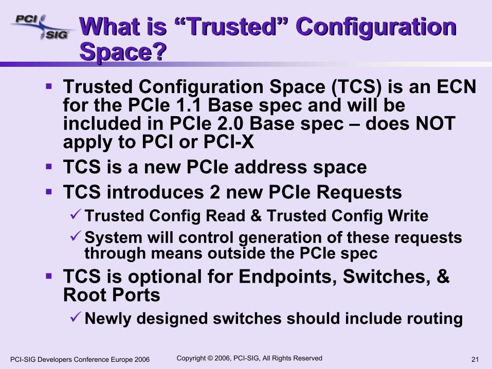
Trusted Configuration Space (TCS) is an ECN for the PCIe 1.1 Base spec and will be included in PCIe 2.0 Base spec – does NOT apply to PCI or PCI-XTCS is a new PCIe address spaceTCS introduces 2 new PCIe Requests
Trusted Config Read & Trusted Config WriteSystem will control generation of these requests through means outside the PCIe spec
TCS is optional for Endpoints, Switches, & Root Ports
Newly designed switches should include routing

Copyright © 2006, PCI-SIG, All Rights Reserved 22PCI-SIG Developers Conference Europe 2006
InterruptsInterruptsPCI introduced INTA#, INTB#, INTC#, INTD# -collectively referred to as INTx
Level sensitiveDecoupled device from CPU interruptSystem controlled INTx to CPU interrupt mappingConfiguration registers
– report A/B/C/D – programmed with CPU interrupt number
PCI Express mimics this via “virtual wire”messages
Assert_INTx and Deassert_INTx
Copyright © 2006, PCI-SIG, All Rights Reserved 23PCI-SIG Developers Conference Europe 2006
MSI & MSI-X ExplainedMSI & MSI-X Explained

Copyright © 2006, PCI-SIG, All Rights Reserved 24PCI-SIG Developers Conference Europe 2006
MSI & MSI-X Apply to ALL PCI-SIG SpecificationsMSI & MSI-X Apply to ALL PCI-SIG Specifications
Implementation of MSI *or* MSI-X is mandatory in both PCI Express and PCI-X
Note recent ECNs allowing MSI-X instead of MSI
Implementation of either MSI or MSI-X is optional in Conventional PCI
Subsequent slides apply to any bus implementation of MSI and MSI-X
Same structures in PCI, PCI-X, and PCI Express
Copyright © 2006, PCI-SIG, All Rights Reserved 25PCI-SIG Developers Conference Europe 2006
Once Enabled, MSI or MSI-X Messages Replace INTxOnce Enabled, MSI or MSI-X Messages Replace INTx
PCI and PCI-X devices stop asserting INTA, INTB, INTC, INTD once MSI or MSI-X mode is enabled
PCI Express devices stop sending Assert_INTx and Deassert_INTx TLPs once MSI or MSI-X mode is enabled
NOTE: Boot devices and any device intended for a non-MSI operating system generally must still support the appropriate INTxsignaling!
Copyright © 2006, PCI-SIG, All Rights Reserved 26PCI-SIG Developers Conference Europe 2006
MSI and MSI-X ExplainedMSI and MSI-X Explained
MSI
Message Signaled Interrupts (MSI) is an optional feature that enables a device function to request service by writing a system-specified data value to a system-specified address (using a PCI DWORD memory write transaction).
System software initializes the message address and message data (referred to as the “vector”) during device configuration, allocating one or more vectors to each MSI-capable function.

Copyright © 2006, PCI-SIG, All Rights Reserved 27PCI-SIG Developers Conference Europe 2006
MSI-X
MSI-X defines a separate optional extension to basic MSI functionality.Many of the characteristics of MSI-X are identical to those of MSI. MSI-X additional capabilities include,
– a larger maximum number of vectors per function– the ability for software to control aliasing, when fewer vectors are
allocated than requested– the ability for each vector to use an independent address and data
value, specified by a table that resides in Memory Space.
MSI and MSI-X ExplainedMSI and MSI-X Explained

Copyright © 2006, PCI-SIG, All Rights Reserved 28PCI-SIG Developers Conference Europe 2006
Per-vector maskingPer-vector masking is managed through a Mask and Pending bit pair per MSI vector or MSI-X Table entry. An MSI vector is masked when its associated Mask bit is set. An MSI-X vector is masked when its associated MSI-X Table entry Mask bit or the MSI-X Function Mask bit is set. While a vector is masked,
– the function is prohibited from sending the associated message,
– and the function must set the associated Pending bit whenever the function would otherwise send the message.
MSI and MSI-X ExplainedMSI and MSI-X Explained
Copyright © 2006, PCI-SIG, All Rights Reserved 29PCI-SIG Developers Conference Europe 2006
MSI-X ECNA function is permitted to implement both MSI and MSI-X, but system software is prohibited from enabling both at the same time. For the sake of software backward compatibility, MSI and MSI-X use separate and independent capability structures. On functions that support both MSI and MSI-X, system software that supports only MSI can still enable and use MSI without any modification.
MSI and MSI-X ExplainedMSI and MSI-X Explained
Copyright © 2006, PCI-SIG, All Rights Reserved 30PCI-SIG Developers Conference Europe 2006
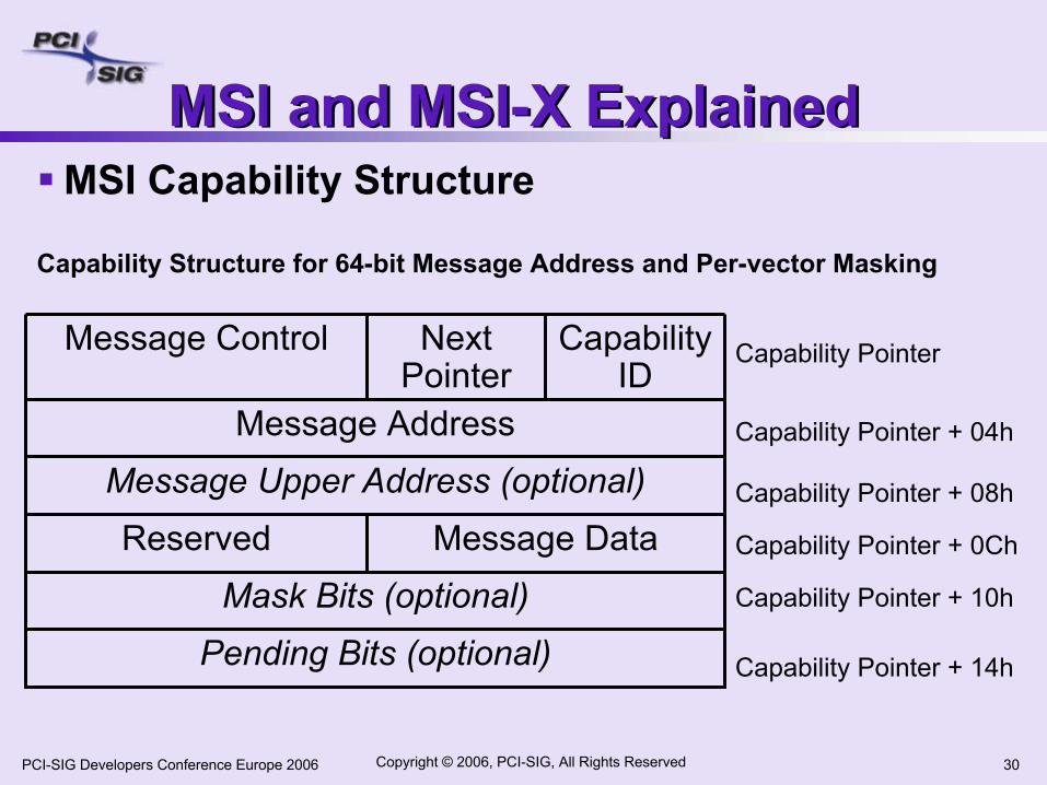
MSI Capability Structure
Pending Bits (optional)Mask Bits (optional)
Message Upper Address (optional)Message Data
Next Pointer
Capability ID
Reserved
Message Address
Message Control Capability Pointer
Capability Pointer + 08h
Capability Pointer + 04h
Capability Pointer + 0Ch
Capability Structure for 64-bit Message Address and Per-vector Masking
Capability Pointer + 10h
Capability Pointer + 14h
MSI and MSI-X ExplainedMSI and MSI-X Explained
Copyright © 2006, PCI-SIG, All Rights Reserved 31PCI-SIG Developers Conference Europe 2006
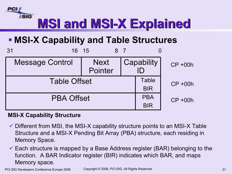
MSI-X Capability and Table Structures
PBABIR
TableBIR
PBA Offset
Next Pointer
Capability ID
Table Offset
Message Control CP +00h
MSI-X Capability Structure
CP +00h
CP +00h
31 16 15 8 7 0
Different from MSI, the MSI-X capability structure points to an MSI-X Table Structure and a MSI-X Pending Bit Array (PBA) structure, each residing in Memory Space.Each structure is mapped by a Base Address register (BAR) belonging to the function. A BAR Indicator register (BIR) indicates which BAR, and maps Memory space.
MSI and MSI-X ExplainedMSI and MSI-X Explained

Copyright © 2006, PCI-SIG, All Rights Reserved 32PCI-SIG Developers Conference Europe 2006
MSI-X Capability and Table Structures
Msg AddressMsg Upper AddrMsg DataVector Ctrl
Msg AddressMsg Upper AddrMsg DataVector Ctrl
Msg AddressMsg Upper AddrMsg DataVector Ctrl
….….
Msg Data
….
Msg Upper Addr Msg Address
….
Vector Ctrl entry 0 Base
MSI-X Table Structure
DWORD3 DWORD2 DWORD1 DWORD0
entry 1 Base +1*16
entry 2 Base +2*16
entry (N-1) Base +(N-1)*16
….. …..
MSI and MSI-X ExplainedMSI and MSI-X Explained

Copyright © 2006, PCI-SIG, All Rights Reserved 33PCI-SIG Developers Conference Europe 2006
MSI-X Capability and Table Structures
Pending Bits ((N-1) div 64)*64 through N-1
Pending Bits 64 through 127
Pending Bits 0 through 63
….
QWORD0 Base
MSI-X PBA Structure
63 62 61 ………. ……….2 1 0
QWORD1 Base + 1*8
QWORD0 Base
QWORD((N-1) div 64) Base+((N-1) div 64)*8
MSI and MSI-X ExplainedMSI and MSI-X Explained
Copyright © 2006, PCI-SIG, All Rights Reserved 34PCI-SIG Developers Conference Europe 2006
Enabling and Sending Message Interrupts
Both MSI and MSI-X are disabled following reset.System configuration software sets either the MSI Enable bit or the MSI-X Enable bit to enable either MSI or MSI-X, but never both simultaneously.Once MSI or MSI-X is enabled, and one or more vectors is unmasked, the function is permitted to send messages.To send a message, a function does a DWORD memory write to the appropriate message address with the appropriate message data.
MSI and MSI-X ExplainedMSI and MSI-X Explained

Copyright © 2006, PCI-SIG, All Rights Reserved 35PCI-SIG Developers Conference Europe 2006
PCI-X ExplainedPCI-X Explained

Copyright © 2006, PCI-SIG, All Rights Reserved 36PCI-SIG Developers Conference Europe 2006
What is PCI-X?What is PCI-X?
“PCI-X is high-performance backward compatible PCI”
PCI-X uses the same PCI architecturePCI-X leverages the same base protocols as PCIPCI-X leverages the same BIOS as PCIPCI-X uses the same connector as PCI.PCI-X and PCI products are interoperablePCI-X uses same software driver models as PCI
PCI-X is faster PCIPCI-X 533 is up to 32 times faster than the original version of PCIPCI-X protocol is more efficient than conventional PCI
Copyright © 2006, PCI-SIG, All Rights Reserved 37PCI-SIG Developers Conference Europe 2006
What is PCI-X 2.0?What is PCI-X 2.0?
Revision 2.0 includes everything from Revision 1.0PCI-X 66
– Same clock speed as fastest conventional PCI– Easier timing and more efficient bus utilization
PCI-X 133– Twice as fast as conventional PCI– Easier timing and more efficient bus utilization
Revision 2.0 introduces 2 new speed gradesPCI-X 266
– “Double data rate” clocking for transfer rates up to 266MHz– Up to 2.13 Gigabytes per second of bandwidth
PCI-X 533– “Quad data rate” clock for transfer rates of up to 533MHz– Up to 4.26 Gigabytes per second of bandwidth
All PCI-X devices are fully backward-compatible to:33 MHz conventional PCI (66 MHz support is optional)All lower PCI-X speeds

Copyright © 2006, PCI-SIG, All Rights Reserved 38PCI-SIG Developers Conference Europe 2006
64-Bit 32-Bit Mode VI/O Slots* MB/s Slots* MB/s 16-Bit Error
Prot Conf Bytes DIM
PCI 33 5V/3.3V
266
133 N/A par 256 N/A
PCI 66 3.3V
533
266 N/A par 256 N/A
PCI-X 66 3.3V
533
266 N/A par or ECC 256 yes
PCI-X 133 (operating at
100 MHz) 3.3V
800
400 N/A par or ECC 256 yes
PCI-X 133 3.3V
1066
533 N/A par or ECC 256 yes
PCI-X 266 1.5V
2133
1066 533 ECC 4K yes
PCI-X 533 1.5V
4266
2133 1066 ECC 4K yes
PCI-X Modes and SpeedsPCI-X Modes and Speeds
* For lower bus speeds, # slots / bus is implementation choice to share bandwidth
Mode 1
Mode 2

Copyright © 2006, PCI-SIG, All Rights Reserved 39PCI-SIG Developers Conference Europe 2006
Registered Bus ProtocolRegistered Bus ProtocolPCI @ 33MHz
30 ns period7 ns setup time
PCI-X registered protocol allocates a full clock period for logic decision
@ 66MHz - 15ns@ 133MHz - 7.5ns
PCI @ 66MHz15 ns period3ns setup time
SenderAssertsSignal
Propagation delay across bus
ReceiverDecodes Logic
ReceiverResponds
Receiverregisters
signal
32
PCI -X Clock
1
PCI Clock, 33 MHz
SenderAssertsSignal
Propagation delay across bus
ReceiverResponds
Receiver DecodesLogic
1 2
SenderAssertsSignal
Propagation delayacross bus
Receiver Decodes Logic
PCI Clock, 66 MHz
321
ReceiverResponds

Copyright © 2006, PCI-SIG, All Rights Reserved 40PCI-SIG Developers Conference Europe 2006
PCI 2.1/2.2PCI 2.1/2.2
PCI-X protocol always takes 2 clocks to “turn around” a control event
Registered Bus ProtocolRegistered Bus Protocol
Register-to-register design allows maximum flight time
LogicLogic
RegReg
I/O BuffersI/O BuffersBoundary ScanBoundary Scan
PCIPCIClockClock
2.1/2.2 2.1/2.2
PCIPCI--XX
PCIPCI--XX RegRegPCIPCIClockClock
Copyright © 2006, PCI-SIG, All Rights Reserved 41PCI-SIG Developers Conference Europe 2006
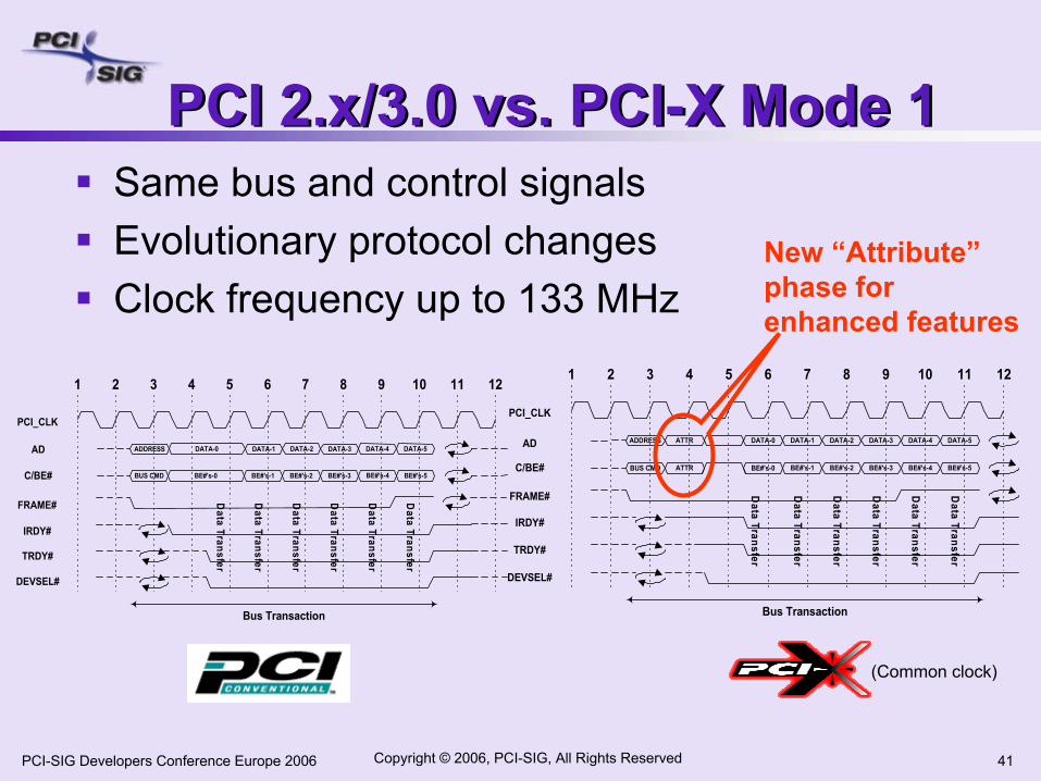
PCI 2.x/3.0 vs. PCI-X Mode 1PCI 2.x/3.0 vs. PCI-X Mode 1Same bus and control signals Evolutionary protocol changesClock frequency up to 133 MHz
PCI_CLK
1 2 3 4 5 6 7 8 9 10 11 12
Data Transfer
Data Transfer
Data Transfer
Data Transfer
Data Transfer
Data Transfer
Bus Transaction
DEVSEL#
TRDY#
IRDY#
FRAME#
BUS CMDC/BE# BE#'s-0ATTR BE#'s-1 BE#'s-2 BE#'s-3 BE#'s-4 BE#'s-5
ADDRESSAD DATA-0 DATA-1 DATA-2 DATA-3 DATA-4ATTR DATA-5
PCI_CLK
1 2 3 4 5 6 7 8 9 10 11 12
Data Transfer
Data Transfer
Data Transfer
Data Transfer
Data Transfer
Data Transfer
Bus Transaction
ADDRESSAD DATA-0 DATA-1 DATA-2 DATA-3 DATA-4 DATA-5
BUS CMDC/BE# BE#'s-0 BE#'s-1 BE#'s-4BE#'s-3BE#'s-2 BE#'s-5
FRAME#
IRDY#
TRDY#
DEVSEL#
(Common clock)
New “Attribute”phase for enhanced features
Copyright © 2006, PCI-SIG, All Rights Reserved 42PCI-SIG Developers Conference Europe 2006
Same bus and control signals PCI-X 266 moves 2x the dataPCI-X 533 moves 4x the dataClock frequency up to 133 MHz
1 2 3 4 5 6 7 8 9 10 11 12
PCI_CLK
TRDY#
IRDY#
FRAME#
BUS CMDC/BE# ATTR
ADDRAD ATTR
Data Transfer
Data Transfer
Data Transfer
Data Transfer
Data Transfer
Data Transfer
1
0 2 3 4 5 61 7 8 9 10 11 12 14 15 16 17 1813 19 20 21 22 23
(Data)
(Strobe)
0 2 31
DEVSEL#
PCI-X 66/133 (Mode 1) PCI-X 533 (Mode 2)
PCI_CLK
1 2 3 4 5 6 7 8 9 10 11
Data Transfer
Data Transfer
Data Transfer
Data Transfer
Data Transfer
Data Transfer
Bus Transaction
DEVSEL#
TRDY#
IRDY#
FRAME#
BUS CMDC/BE# BE#'s-0ATTR BE#'s-1 BE#'s-2 BE#'s-3 BE#'s-4 BE#'s-5
ADDRESSAD DATA-0 DATA-1 DATA-2 DATA-3 DATA-4ATTR DATA-5
PCI-X 66/133 (Mode 1) vs. PCI-X 266/533 (Mode 2)PCI-X 66/133 (Mode 1) vs. PCI-X 266/533 (Mode 2)
4 transfers per clock cycle
source-synchronous data strobes share C/BE pins
Copyright © 2006, PCI-SIG, All Rights Reserved 43PCI-SIG Developers Conference Europe 2006
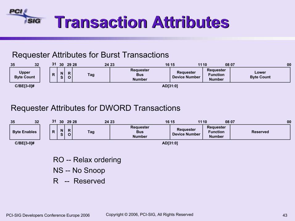
Transaction AttributesTransaction Attributes
RO -- Relax orderingNS -- No SnoopR -- Reserved
UpperByte Count
C/BE[3-0]# AD[31:0]
LowerByte Count
RequesterBus
Number
RequesterDevice Number
RequesterFunctionNumber
TagNS
RO
R
000708101115162324313235 282930
Requester Attributes for Burst Transactions
Requester Attributes for DWORD Transactions
Byte Enables
C/BE[3-0]# AD[31:0]
ReservedRequester
BusNumber
RequesterDevice Number
RequesterFunctionNumber
TagNS
RO
R
000708101115162324313235 282930

Copyright © 2006, PCI-SIG, All Rights Reserved 44PCI-SIG Developers Conference Europe 2006
Transaction AttributesTransaction Attributes
SCM -- Split Completion MessageSCE -- Split Completion ErrorBCM -- Byte Count ModifiedR -- Reserved
UpperByte Count
LowerByte Count
CompleterBus
Number
CompleterDeviceNumber
CompleterFunctionNumber
R
00070810111516232431
SCM
2829BCM
SCE
30
AD[31:0]C/BE[3:0]#
3 0
RequesterBus
Number
RequesterDevice
Number
RequesterFunctionNumber
Lower Address [6:0]BUS CMD
00070810111516232431
C/BE[3-0]#
TagR RO R
062930 28
AD[31:0]
03
R
Split Completion Address
Completer Attributes
RO -- Relaxed ordering

Copyright © 2006, PCI-SIG, All Rights Reserved 45PCI-SIG Developers Conference Europe 2006
Split TransactionsSplit TransactionsBus efficiency of Read almost as good as Write Split Completion routed back to requester across bridges using initiator’s number and bus numberSplit Transaction components
Step 1. Requester requests bus and arbiter grants busStep 2. Requester initiates transactionStep 3. Target (completer) communicates intent with new target termination, Split ResponseStep 4. Completer executes transaction internallyStep 5. Completer requests bus and arbiter grants busStep 6. Completer initiates Split Completion

Copyright © 2006, PCI-SIG, All Rights Reserved 46PCI-SIG Developers Conference Europe 2006
Split TransactionsSplit Transactions
Target
Initiater
Completer B
Target
Initiater
Requester A
PCI Bus
Address,Memory Read
RequesterAttributes
REQGNT
DataSplit Reponse
SplitCompletion
CompleterAttributes DATA
REQGNT(Requester's
Attribute)
ImmediateResponse
SplitTransactionCompleter
SplitTransactionRequester

Copyright © 2006, PCI-SIG, All Rights Reserved 47PCI-SIG Developers Conference Europe 2006
Efficient PCI-X ProtocolEfficient PCI-X Protocol
25
50
100
125
150
175
200
225
250
275
Number of Load Exerciser Cards
1 2 3 4 5
Ban
dwid
th M
egaB
ytes
/sec
50%
60%
70%
80%
90%
100%
10%
20%
30%
40%
Percent of Total Bandw
idth25
50
100
125
150
175
200
225
250
275
Number of Load Exerciser Cards
21
50%
60%
70%
80%
90%
100%
10%
20%
30%
40%
Percent of Total BandW
idth
System Overhead-- Scheduling
Transaction Overhead -- Addressing and Routing
Transaction Data Payload -- Actual user data
Idle Time-- Unused BW
TransactionData Payload-- Actual userdata
Idle Time-- Unused BW
System Overhead-- Scheduling
Transaction Overhead -- Addressing and Routing
Ban
dwid
th M
egaB
ytes
/sec
Bandwidth Usage with Conventional PCI Protocols Bandwidth Usage with PCI-X Protocols,included in PCI-X 2.0
The PCI-X protocol is more efficient than traditional PCI.

Copyright © 2006, PCI-SIG, All Rights Reserved 48PCI-SIG Developers Conference Europe 2006
PCI-X I/O Signaling VoltagesPCI-X I/O Signaling Voltages
PCI-X 66 and 1333.3V signalingCard-edge connector keyed for “3.3V” or “Universal” signaling
PCI-X 266 and 533 use combination of 3.3V I/O and new 1.5V I/O
Control signals use 3.3V I/OData and strobe signals use 1.5V I/O
– Faster signaling rates– Point-to-point and electrically terminated for improved noise
immunity– New interface low-power state to manage interface power– I/O buffer change only
• Same system supply voltages• Automatic selection by devices at power-up
Card-edge connector keyed for “3.3V signaling”

Copyright © 2006, PCI-SIG, All Rights Reserved 49PCI-SIG Developers Conference Europe 2006
PCI-X 2.0 Offers Improved RAS FeaturesPCI-X 2.0 Offers Improved RAS Features
Parity protectionProvides full compatibility with conventional PCI and PCI-X 1.0
ECC protection new in PCI-X 2.0Covers both header and payloadProvides automatic single bit error recoveryDetects all double bit errorsDetects all errors in single nibbleDetects phase errors (e.g. missed strobe or extra strobe)Adds no additional latency over parityRequired for Mode 2; optional for Mode 1
Enhanced data-error recovery optionsAvailable both for Mode 1 and Mode 2

Copyright © 2006, PCI-SIG, All Rights Reserved 50PCI-SIG Developers Conference Europe 2006
PCI X 2.0 is Software Compatible with Conventional PCICompatible with Conventional PCI
No OS or driver change requiredNew configuration registers default to functional valuesOptional performance tuning registers Other configuration registers unchangedNo device programming model changes required
Optional improved error handlingEnables smart device and new driver to recover from PERR# event

Copyright © 2006, PCI-SIG, All Rights Reserved 51PCI-SIG Developers Conference Europe 2006
PCI Express OverviewPCI Express Overview

Copyright © 2006, PCI-SIG, All Rights Reserved 52PCI-SIG Developers Conference Europe 2006
PCIe™ Architecture PrimerPCIePCIe™™ Architecture PrimerArchitecture PrimerCost EffectiveCost Effective••PCI cost structure at system PCI cost structure at system levellevel
••Low power, no sidebandsLow power, no sidebands
••Commodity ingredients: FRCommodity ingredients: FR--4 4 PCBs, simple connectors, low PCBs, simple connectors, low manufacturing costsmanufacturing costs
Scalable/Extensible I/OScalable/Extensible I/O••Scalable in performance and Scalable in performance and feature setfeature set
••Suitable for over 10Suitable for over 10--year year horizonhorizon
••HighHigh--end and mainstream end and mainstream applicationsapplications
Multiple Market Multiple Market Segments/ApplicationsSegments/Applications••Mobile, desktop, server and Mobile, desktop, server and communication devicescommunication devices
••ChipChip--toto--chip, boardchip, board--toto--board, board, modules, docking, cablesmodules, docking, cables
Compatibility & Compatibility & Smooth Migration Smooth Migration
••Preserves investments in PCI Preserves investments in PCI ecosystemecosystem
••Path to future enhancements Path to future enhancements and proliferationsand proliferations
Serial, point-to-point interconnect of choice for all platform applicationsSerial, pointSerial, point--toto--point interconnect of choice for all platform applicationspoint interconnect of choice for all platform applications
CPUCPU
Legacy Slots

Copyright © 2006, PCI-SIG, All Rights Reserved 53PCI-SIG Developers Conference Europe 2006
PCIe Architecture FeaturesPCIe Architecture FeaturesPCIe Architecture FeaturesPCI Compatibility
Configuration and PCI software driver modelPCI power management software compatible
PerformanceScalable frequency (2.5-5GT/s)Scalable width (x1, x4, x8, x16)Low latency and highest utilization (BW/pin)
Physical InterfacePoint-to-point, dual-simplexDifferential low voltage signalingEmbedded clockingSupports connectors, modules, cables
ProtocolFully packetized split-transactionCredit-based flow controlHierarchical topology support Virtual channel mechanism
Advanced CapabilitiesCRC-based data integrity, hot plug, error logging
Enhanced Configuration Space
Extensions and bridges into other architectures

Copyright © 2006, PCI-SIG, All Rights Reserved 54PCI-SIG Developers Conference Europe 2006
PCIe Protocol OverviewPCIe Protocol OverviewPCI-X Address/Attribute phases:
Evolved into the PCIe Packet Header:

Copyright © 2006, PCI-SIG, All Rights Reserved 55PCI-SIG Developers Conference Europe 2006
The packet bytes get converted to 8b/10b and serialized
PCIe Protocol OverviewPCIe Protocol Overview

Copyright © 2006, PCI-SIG, All Rights Reserved 56PCI-SIG Developers Conference Europe 2006
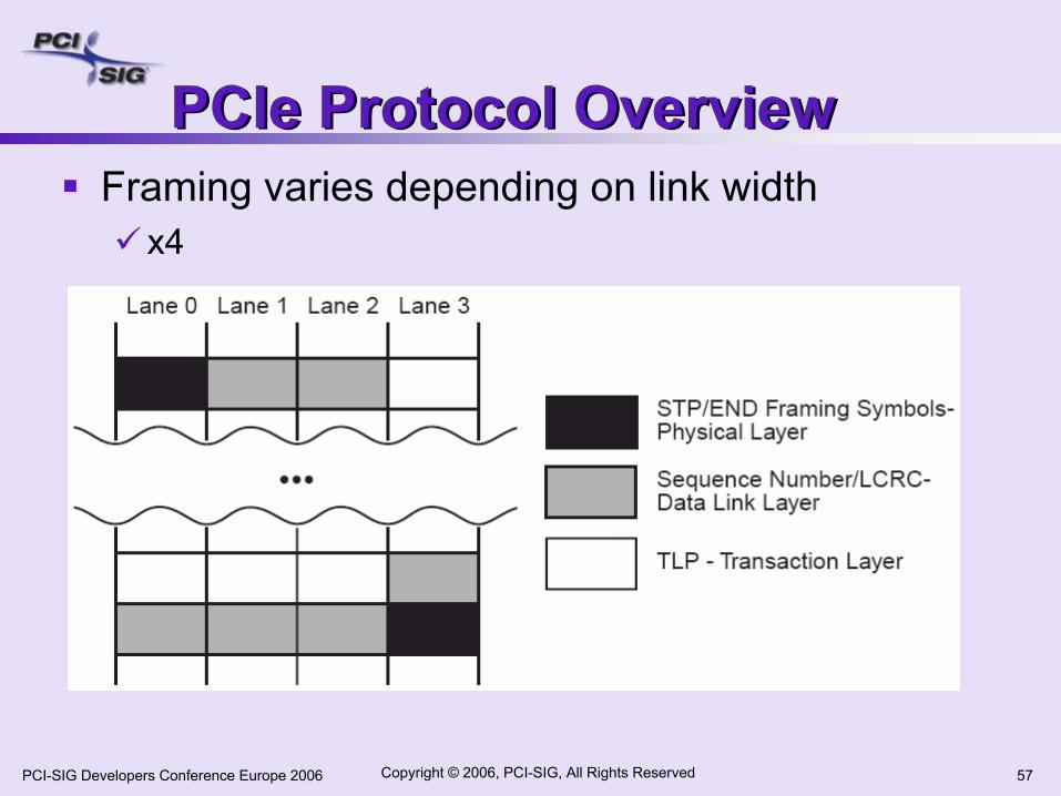
Framing varies depending on link widthx1
PCIe Protocol OverviewPCIe Protocol Overview
Copyright © 2006, PCI-SIG, All Rights Reserved 57PCI-SIG Developers Conference Europe 2006
PCIe Protocol OverviewPCIe Protocol OverviewFraming varies depending on link width
x4

Copyright © 2006, PCI-SIG, All Rights Reserved 58PCI-SIG Developers Conference Europe 2006
PCIe Architecture SpecificationsPCIe Architecture SpecificationsPCIe Architecture Specifications
Form Factors:– Card– Mini Card– ExpressModule– Wireless Card (WIP)– Cable (WIP)
Data Link
Transaction
Software
Physical
Mechanical
BBaassee
– BaseElectricalProtocolConfiguration
– Bridge– I/O Virtualization
(WIP)
Layered, scalable architecture
Performance matched to applications
Innovative form factors
Related Documents