Copyright 2001 A grawal & Bushnel l Hyderabad, July 27-29, 20 06 (Day 2) 1 Combinational ATPG ATPG problem Example Algorithms Multi-valued algebra D-algorithm Podem Other algorithms ATPG system Summary

Welcome message from author
This document is posted to help you gain knowledge. Please leave a comment to let me know what you think about it! Share it to your friends and learn new things together.
Transcript

Copyright 2001 Agrawal & Bushnell
Hyderabad, July 27-29, 2006 (Day 2) 1
Combinational ATPGCombinational ATPG
ATPG problem Example Algorithms
Multi-valued algebra D-algorithm Podem Other algorithms
ATPG system Summary
Copyright 2001 Agrawal & Bushnell
Hyderabad, July 27-29, 2006 (Day 2) 2
ATPG ProblemATPG Problem
ATPG: Automatic test pattern generation Given
A circuit (usually at gate-level) A fault model (usually stuck-at type)
Find A set of input vectors to detect all modeled faults.
Core solution: Find a test vector for a given fault. Combine the “core solution” with a fault
simulator into an ATPG system.

Copyright 2001 Agrawal & Bushnell
Hyderabad, July 27-29, 2006 (Day 2) 3
What is a Test?What is a Test?
X100101XX
Stuck-at-0 fault
1/0
Fault activation
Path sensitization
Primary inputs(PI)
Primary outputs(PO)
Combinational circuit
1/0
Fault effect

Copyright 2001 Agrawal & Bushnell
Hyderabad, July 27-29, 2006 (Day 2) 4
Multiple-Valued AlgebrasMultiple-Valued AlgebrasSymbol
DD01X
G0G1F0F1
AlternativeRepresentation
1/00/10/01/1X/X0/X1/XX/0X/1
FaultyCircuit
0101XXX01
Fault-freecircuit
1001X01XX
Roth’sAlgebra
Muth’sAdditions
Copyright 2001 Agrawal & Bushnell
Hyderabad, July 27-29, 2006 (Day 2) 5
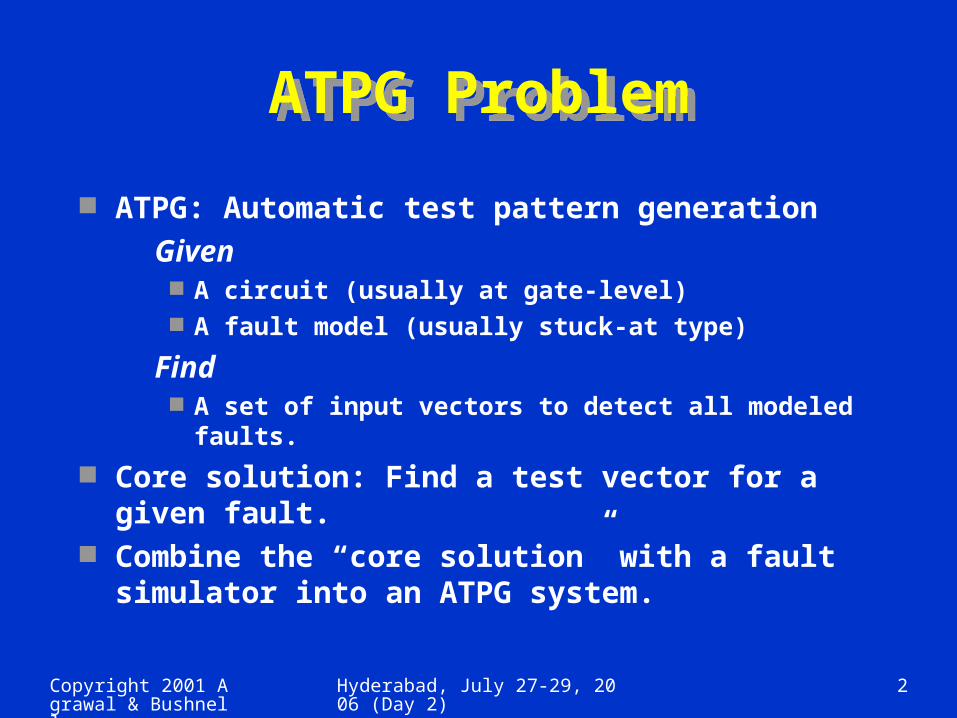
An ATPG ExampleAn ATPG Example1 Fault activation2 Path sensitization3 Line justification
1D

Copyright 2001 Agrawal & Bushnell
Hyderabad, July 27-29, 2006 (Day 2) 6
ATPG Example (Cont.)ATPG Example (Cont.)1 Fault activation2 Path sensitization3 Line justification
1 D
D
D
D
Path from fault site to a primary output
Copyright 2001 Agrawal & Bushnell
Hyderabad, July 27-29, 2006 (Day 2) 7
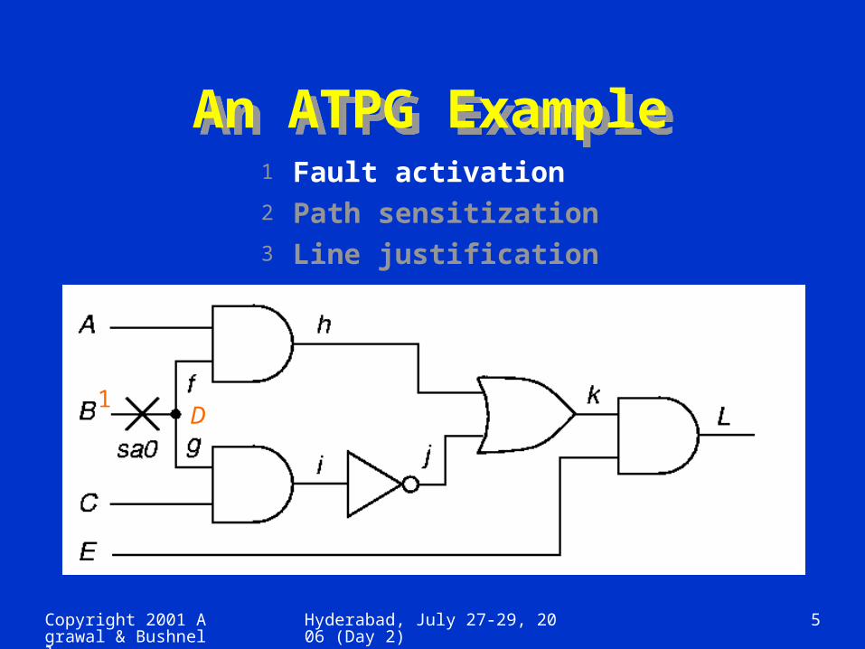
ATPG Example (Cont.)ATPG Example (Cont.)1 Fault activation2 Path sensitization3 Line justification
1 D
D
D
D
1
0
11
1
Conflict
1
Copyright 2001 Agrawal & Bushnell
Hyderabad, July 27-29, 2006 (Day 2) 8
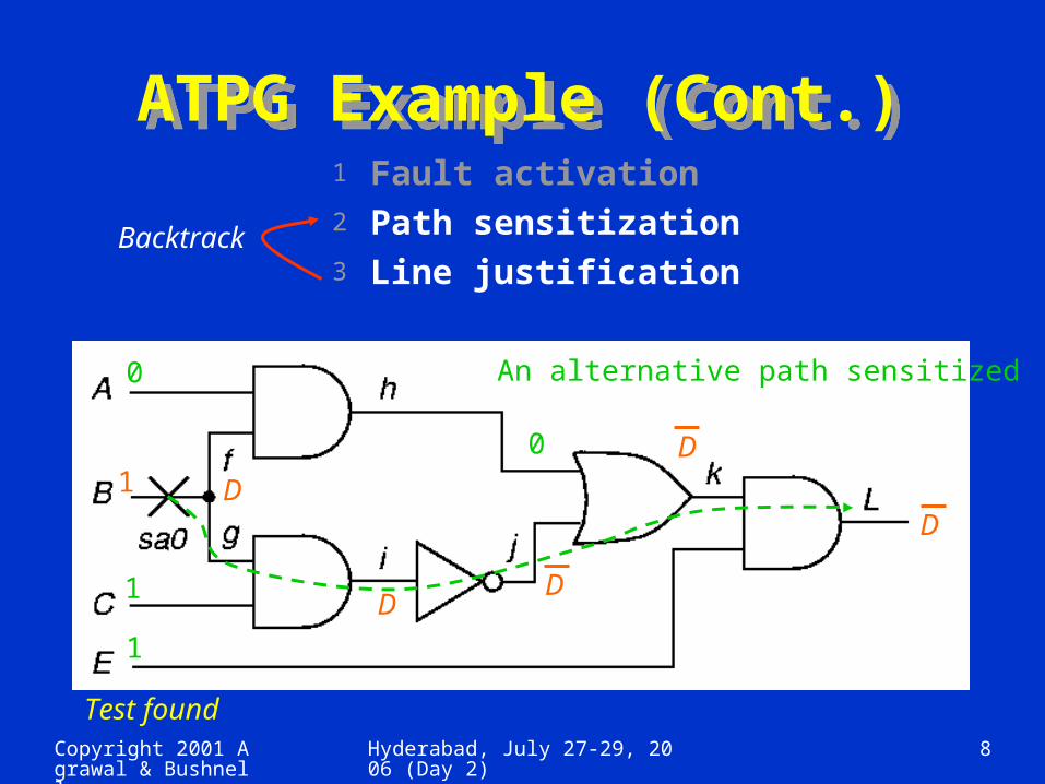
ATPG Example (Cont.)ATPG Example (Cont.)1 Fault activation2 Path sensitization3 Line justification
1 D
D
D
D
0
0
1
1
Backtrack
D
Test found
An alternative path sensitized
Copyright 2001 Agrawal & Bushnell
Hyderabad, July 27-29, 2006 (Day 2) 9
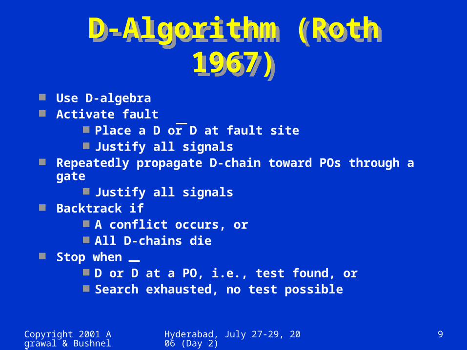
D-Algorithm (Roth 1967)
D-Algorithm (Roth 1967)
Use D-algebra Activate fault
Place a D or D at fault site Justify all signals
Repeatedly propagate D-chain toward POs through a gate Justify all signals
Backtrack if A conflict occurs, or All D-chains die
Stop when D or D at a PO, i.e., test found, or Search exhausted, no test possible

Copyright 2001 Agrawal & Bushnell
Hyderabad, July 27-29, 2006 (Day 2) 10
Example: Fault A sa0Example: Fault A sa0 Step 1 – Fault activation – Set A = 1
D1 D
D-frontier = {e, h}

Copyright 2001 Agrawal & Bushnell
Hyderabad, July 27-29, 2006 (Day 2) 11
Example ContinuedExample Continued
D1
0
D
Step 2 – D-Drive – Set f = 0
D

Copyright 2001 Agrawal & Bushnell
Hyderabad, July 27-29, 2006 (Day 2) 12
Example ContinuedExample Continued
D1
0
D
Step 3 – D-Drive – Set k = 1
D
1
D

Copyright 2001 Agrawal & Bushnell
Hyderabad, July 27-29, 2006 (Day 2) 13
Example ContinuedExample Continued
D1
0
D
Step 4 – Consistency – Set g = 1
D
1
D1

Copyright 2001 Agrawal & Bushnell
Hyderabad, July 27-29, 2006 (Day 2) 14
Example ContinuedExample Continued
D1
0
D
Step 5 – Consistency – f = 0 Already set
D
1
D1

Copyright 2001 Agrawal & Bushnell
Hyderabad, July 27-29, 2006 (Day 2) 15
Example ContinuedExample Continued
D1
0
D
Step 6 – Consistency – Set c = 0, Set e = 0
D
1
D1
0
0
Copyright 2001 Agrawal & Bushnell
Hyderabad, July 27-29, 2006 (Day 2) 16
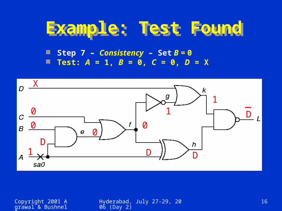
Example: Test FoundExample: Test Found
D1
0
X
D
Step 7 – Consistency – Set B = 0 Test: A = 1, B = 0, C = 0, D = X
D
1
D1
0
0
0

Copyright 2001 Agrawal & Bushnell
Hyderabad, July 27-29, 2006 (Day 2) 17
Podem (Goel, 1981)Podem (Goel, 1981) Podem: Path oriented decision making Step 1: Define an objective (fault activation, D-drive, or line
justification) Step 2: Backtrace from site of objective to PIs (use
testability measures guidance) to determine a value for a PI Step 3: Simulate logic with new PI value
If objective not accomplished but is possible, then continue backtrace to another PI (step 2)
If objective accomplished and test not found, then define new objective (step 1)
If objective becomes impossible, try alternative backtrace (step 2)
Use X-PATH-CHECK to test whether D-frontier still there – a path of X’s from a D-frontier to a PO must exist.

Copyright 2001 Agrawal & Bushnell
Hyderabad, July 27-29, 2006 (Day 2) 18
Podem ExamplePodem Example
(9, 2)
S-a-1
1. Objective “0”
0
2. Backtrace “A=0”3. Logic simulation for A=0
4. Objective possible but not accomplished

Copyright 2001 Agrawal & Bushnell
Hyderabad, July 27-29, 2006 (Day 2) 19
Podem Example (Cont.)Podem Example (Cont.)
(9, 2)
S-a-1
1. Objective “0”
0
5. Backtrace “B=0”6. Logic simulation for A=0, B=0
7. Objective possible but not accomplished
00
0

Copyright 2001 Agrawal & Bushnell
Hyderabad, July 27-29, 2006 (Day 2) 20
Podem Example (Cont.)Podem Example (Cont.)
(9, 2)
S-a-1
1. Objective “0”
0
8. Backtrace “E=0”9. Logic simulation for E=0
10. Objective possible but not accomplished
00
0
0
0

Copyright 2001 Agrawal & Bushnell
Hyderabad, July 27-29, 2006 (Day 2) 21
Podem Example (Cont.)Podem Example (Cont.)
(9, 2)
S-a-1
1. Objective “0”
0
11. Backtrace “D=0”
12. Logic simulation for D=0
13. Objective accomplished
00
0
0
0
0
0
Copyright 2001 Agrawal & Bushnell
Hyderabad, July 27-29, 2006 (Day 2) 22
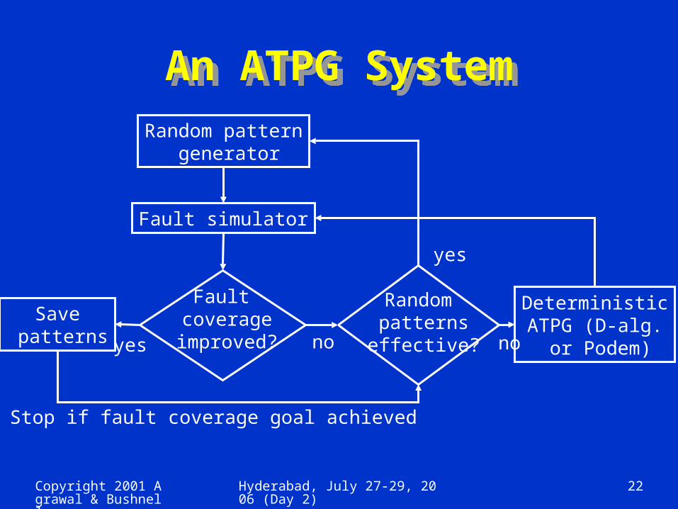
An ATPG SystemAn ATPG SystemRandom pattern
generator
Fault simulator
Fault coverage improved?
Random patterns
effective?
Save patterns
DeterministicATPG (D-alg. or Podem)yes no
yes
no
Stop if fault coverage goal achieved
Copyright 2001 Agrawal & Bushnell
Hyderabad, July 27-29, 2006 (Day 2) 23
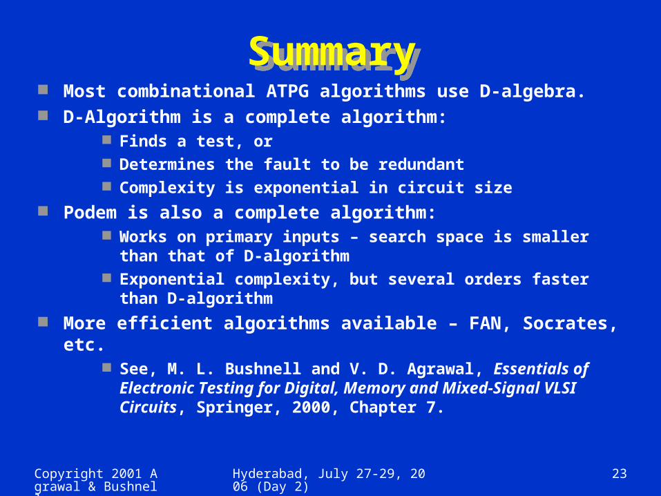
SummarySummary Most combinational ATPG algorithms use D-algebra. D-Algorithm is a complete algorithm:
Finds a test, or Determines the fault to be redundant Complexity is exponential in circuit size
Podem is also a complete algorithm: Works on primary inputs – search space is smaller than that of
D-algorithm Exponential complexity, but several orders faster than D-
algorithm More efficient algorithms available – FAN, Socrates, etc.
See, M. L. Bushnell and V. D. Agrawal, Essentials of Electronic Testing for Digital, Memory and Mixed-Signal VLSI Circuits, Springer, 2000, Chapter 7.

Copyright 2001 Agrawal & Bushnell
Hyderabad, July 27-29, 2006 (Day 2) 24
Sequential ATPGSequential ATPG

Copyright 2001 Agrawal & Bushnell
Hyderabad, July 27-29, 2006 (Day 2) 25
Sequential ATPGSequential ATPG
A sequential circuit has memory in addition to combinational logic.
Test for a fault in a sequential circuit is a sequence of vectors, which
Initializes the circuit to a known state Activates the fault, and Propagates the fault effect to a primary output
Methods of sequential circuit ATPG Time-frame expansion methods Simulation-based methods
Copyright 2001 Agrawal & Bushnell
Hyderabad, July 27-29, 2006 (Day 2) 26
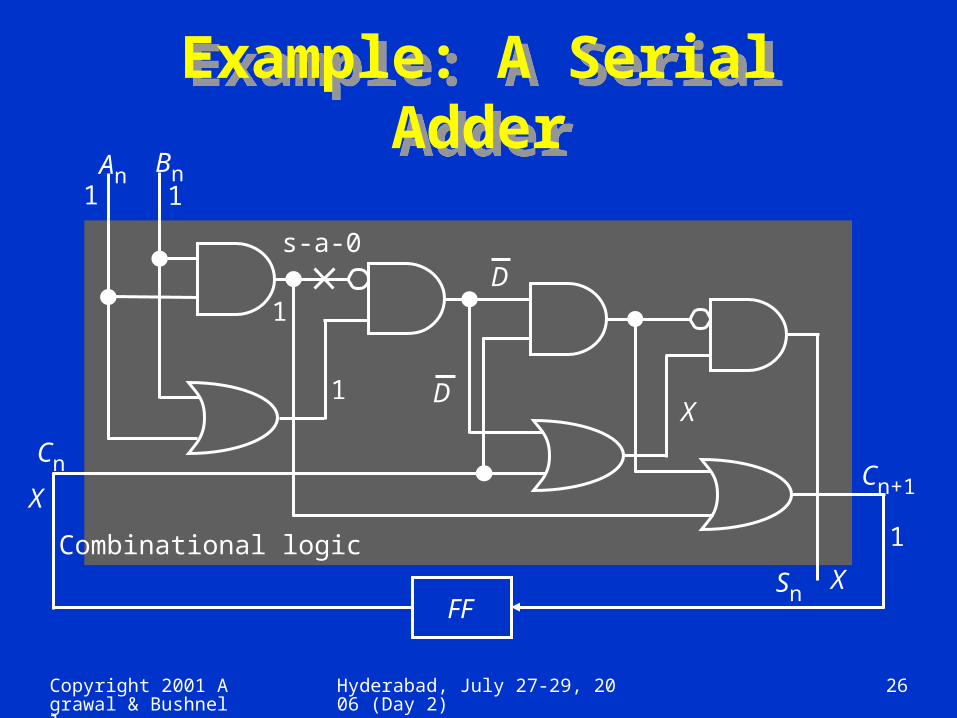
Example: A Serial Adder
Example: A Serial Adder
FF
An Bn
Cn Cn+1
Sn
s-a-0
11
1
1
1
X
X
X
D
D
Combinational logic
Copyright 2001 Agrawal & Bushnell
Hyderabad, July 27-29, 2006 (Day 2) 27
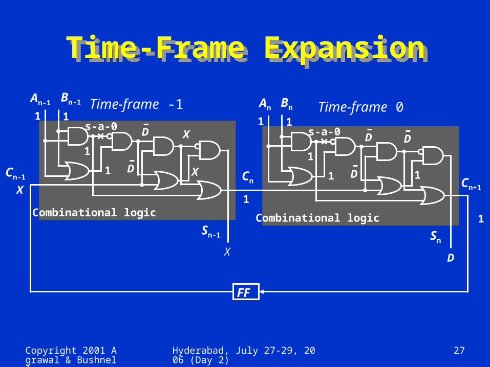
Time-Frame ExpansionTime-Frame Expansion
An Bn
FF
Cn Cn+1
1X
X
Sn
s-a-011
1
1
D
D
Combinational logicSn-1
s-a-011
1
1 X
D
D
Combinational logic
Cn-1
1
1
D
D
X
An-1 Bn-1 Time-frame -1 Time-frame 0

Copyright 2001 Agrawal & Bushnell
Hyderabad, July 27-29, 2006 (Day 2) 28
Concept of Time-Frames
Concept of Time-Frames
If the test sequence for a single stuck-at fault contains n vectors,
Replicate combinational logic block n times Place fault in each block Generate a test for the multiple stuck-at fault using
combinational ATPG with 9-valued logic
Comb.block
Fault
Time-frame
0
Time-frame
-1
Time-frame-n+1
Unknownor givenInit. state
Vector 0Vector -1Vector -n+1
PO 0PO -1PO -n+1
Statevariables
Nextstate
Copyright 2001 Agrawal & Bushnell
Hyderabad, July 27-29, 2006 (Day 2) 29
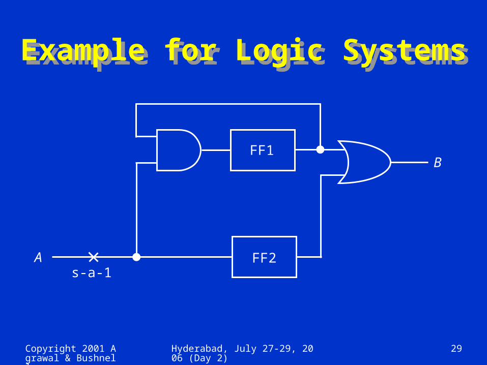
Example for Logic Systems
Example for Logic Systems
FF2
FF1
A
B
s-a-1

Copyright 2001 Agrawal & Bushnell
Hyderabad, July 27-29, 2006 (Day 2) 30
Five-Valued Logic (Roth)0,1, D, D, X
Five-Valued Logic (Roth)0,1, D, D, X
A
B
X
X
X
0
s-a-1
D
A
B
X X
X
0
s-a-1
D
FF1 FF1
FF2 FF2D D
Time-frame -1 Time-frame 0
Copyright 2001 Agrawal & Bushnell
Hyderabad, July 27-29, 2006 (Day 2) 31
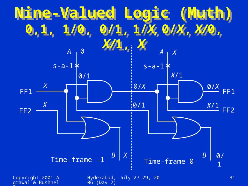
Nine-Valued Logic (Muth)0,1, 1/0, 0/1, 1/X, 0/X, X/0, X/1,
X
Nine-Valued Logic (Muth)0,1, 1/0, 0/1, 1/X, 0/X, X/0, X/1,
X
B
X
0/1
A
B
0/X 0/X
0/1
X
s-a-1X/1
FF1
FF20/1 X/1
Time-frame -1 Time-frame 0
A
X
X
0
s-a-1
FF1
FF2

Copyright 2001 Agrawal & Bushnell
Hyderabad, July 27-29, 2006 (Day 2) 32
Implementation of ATPG
Implementation of ATPG
Select a PO for fault detection based on drivability analysis. Place a logic value, 1/0 or 0/1, depending on fault type and
number of inversions. Justify the output value from PIs, considering all necessary paths
and adding backward time-frames. If justification is impossible, then use drivability to select another
PO and repeat justification. If the procedure fails for all reachable POs, then the fault is
untestable. If 1/0 or 0/1 cannot be justified at any PO, but 1/X or 0/X can be
justified, the the fault is potentially detectable.

Copyright 2001 Agrawal & Bushnell
Hyderabad, July 27-29, 2006 (Day 2) 33
Drivability ExampleDrivability Example
d(0/1) = 4d(1/0) =
(CC0, CC1)= (6, 4)
s-a-1
(4, 4)
(10, 15)
(11, 16)
(10, 16)(22, 17)
(17, 11)
(5, 9)
d(0/1) = 9d(1/0) =
d(0/1) = 109d(1/0) =
d(0/1) = 120d(1/0) = 27
d(0/1) = d(1/0) = 32
(6, 10) 8
8
8
8
FF
d(0/1) = d(1/0) = 20
8
CC0 and CC1 are SCOAP combinational controllabilities
d(0/1) and d(1/0) of a line are effort measures for driving a specific fault effect to that line

Copyright 2001 Agrawal & Bushnell
Hyderabad, July 27-29, 2006 (Day 2) 34
Complexity of ATPGComplexity of ATPG Synchronous circuit – All flip-flops controlled by clocks; PI and
PO synchronized with clock: Cycle-free circuit – No feedback among flip-flops: Test
generation for a fault needs no more than dseq + 1 time-frames, where dseq is the sequential depth.
Cyclic circuit – Contains feedback among flip-flops: May need 9Nff time-frames, where Nff is the number of flip-flops.
Asynchronous circuit – Higher complexity!
Time-Frame
0
Time-Framemax-1
Time-Framemax-2
Time-Frame
-2
Time-Frame
-1
S0S1S2S3Smax
max = Number of distinct vectors with 9-valued elements = 9Nff
Copyright 2001 Agrawal & Bushnell
Hyderabad, July 27-29, 2006 (Day 2) 35
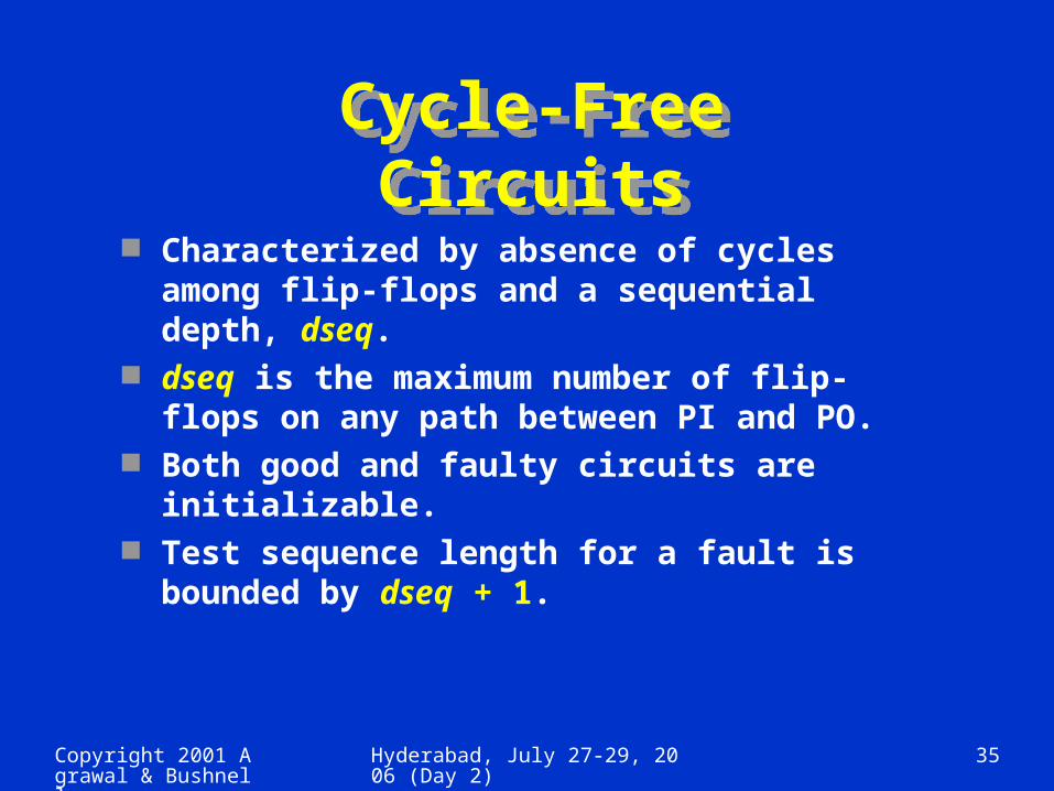
Cycle-Free Circuits
Cycle-Free Circuits
Characterized by absence of cycles among flip-flops and a sequential depth, dseq.
dseq is the maximum number of flip-flops on any path between PI and PO.
Both good and faulty circuits are initializable. Test sequence length for a fault is bounded
by dseq + 1.
Copyright 2001 Agrawal & Bushnell
Hyderabad, July 27-29, 2006 (Day 2) 36
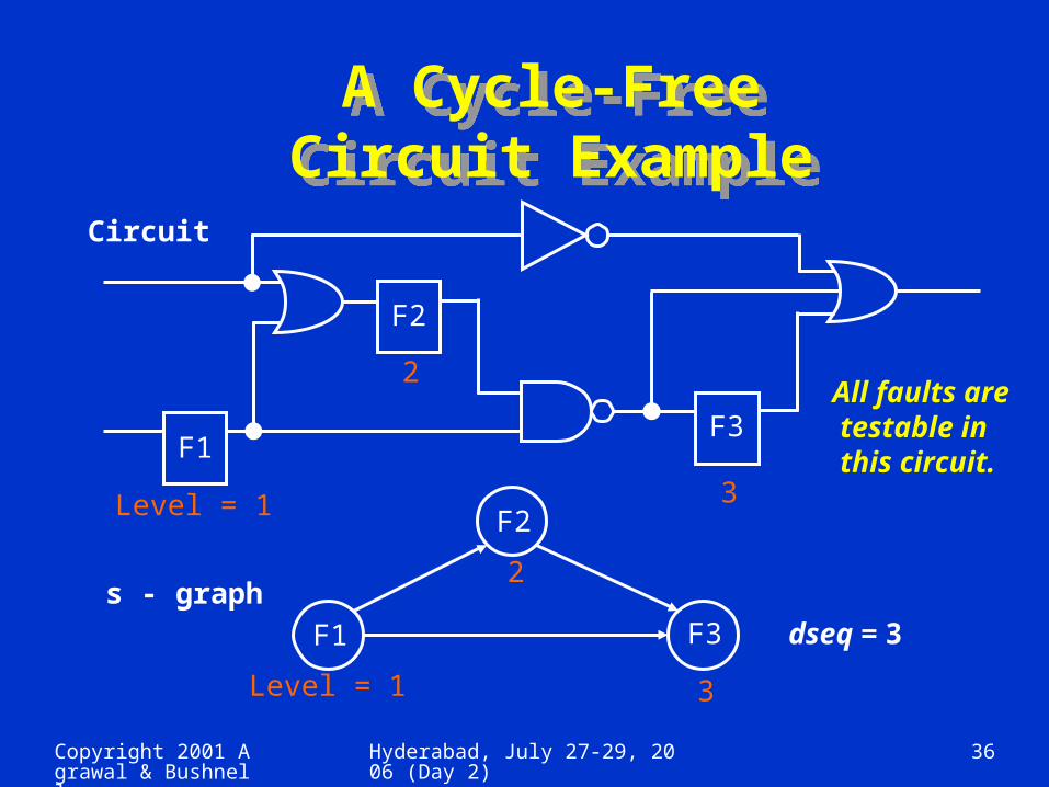
A Cycle-Free Circuit Example
A Cycle-Free Circuit Example
F1
F2
F3
Level = 1
2
F1
F2
F3
Level = 1
2
3
3
dseq = 3s - graph
Circuit
All faults are testable in this circuit.
Copyright 2001 Agrawal & Bushnell
Hyderabad, July 27-29, 2006 (Day 2) 37
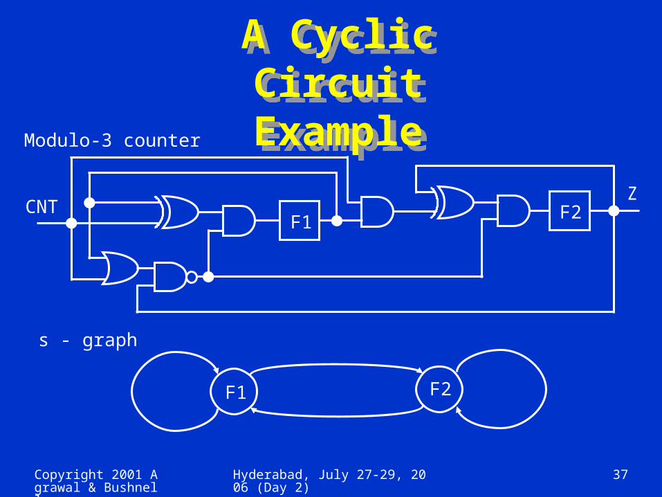
A Cyclic Circuit
Example
A Cyclic Circuit
Example
F1 F2CNTZ
Modulo-3 counter
s - graph
F1 F2

Copyright 2001 Agrawal & Bushnell
Hyderabad, July 27-29, 2006 (Day 2) 38
Modulo-3 Counter
Modulo-3 Counter
Cyclic structure – Sequential depth is undefined. Circuit is not initializable. No tests can be generated for
any stuck-at fault. After expanding the circuit to 9Nff = 81, or fewer, time-frames
ATPG program calls any given target fault untestable. Circuit can only be functionally tested by multiple
observations. Functional tests, when simulated, give no fault coverage.
Copyright 2001 Agrawal & Bushnell
Hyderabad, July 27-29, 2006 (Day 2) 39
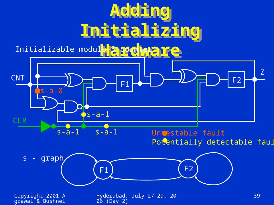
Adding Initializing Hardware
Adding Initializing Hardware
F1 F2CNTZ
Initializable modulo-3 counter
s - graph
F1 F2
CLR
s-a-0
s-a-1
s-a-1s-a-1 Untestable faultPotentially detectable faults

Copyright 2001 Agrawal & Bushnell
Hyderabad, July 27-29, 2006 (Day 2) 40
Benchmark Circuits
Benchmark Circuits
CircuitPIPOFFGatesStructureSeq. depthTotal faultsDetected faultsPotentially detected faultsUntestable faultsAbandoned faultsFault coverage (%)Fault efficiency (%)Max. sequence lengthTotal test vectorsGentest CPU s (Sparc 2)
s1196 14 14 18 529
Cycle-free 412421239 0 3 0
99.8 100.0
3 313 10
s1238 14 14 18 508
Cycle-free 413551283 0 72 0
94.7 100.0
3 308 15
s1488 8 19 6 653
Cyclic--
14861384 2 26 76
93.1 94.8
24 52519941
s1494 8 19 6 647
Cyclic--
15061379 2 30 97
91.6 93.4
28 55919183

Copyright 2001 Agrawal & Bushnell
Hyderabad, July 27-29, 2006 (Day 2) 41
SummarySummary Combinational ATPG algorithms are extended:
Time-frame expansion unrolls time as combinational array Nine-valued logic system Justification via backward time
Cycle-free circuits: Require at most dseq + 1 time-frames Always initializable
Cyclic circuits: May need 9Nff time-frames Circuit must be initializable Partial scan can make circuit cycle-free
Asynchronous circuits: Not discussed See, M. L. Bushnell and V. D. Agrawal, Essentials of Electronic
Testing for Digital, Memory and Mixed-Signal VLSI Circuits, Springer, 2000, Chapter 8.

Copyright 2001 Agrawal & Bushnell
Hyderabad, July 27-29, 2006 (Day 2) 42
Exercise 4Exercise 4
For the circuit shown above Derive a test for the stuck-at-1 fault at the output of
the AND gate. Using the parallel fault simulation algorithm,
determine which of the four primary input faults are detectable by the test derived above.
s-a-1

Copyright 2001 Agrawal & Bushnell
Hyderabad, July 27-29, 2006 (Day 2) 43
Exercise 4: AnswerExercise 4: Answer
s-a-1
0 DD
0
0
■ A test for the stuck-at-1 fault shown in the diagram is 00.
Copyright 2001 Agrawal & Bushnell
Hyderabad, July 27-29, 2006 (Day 2) 44
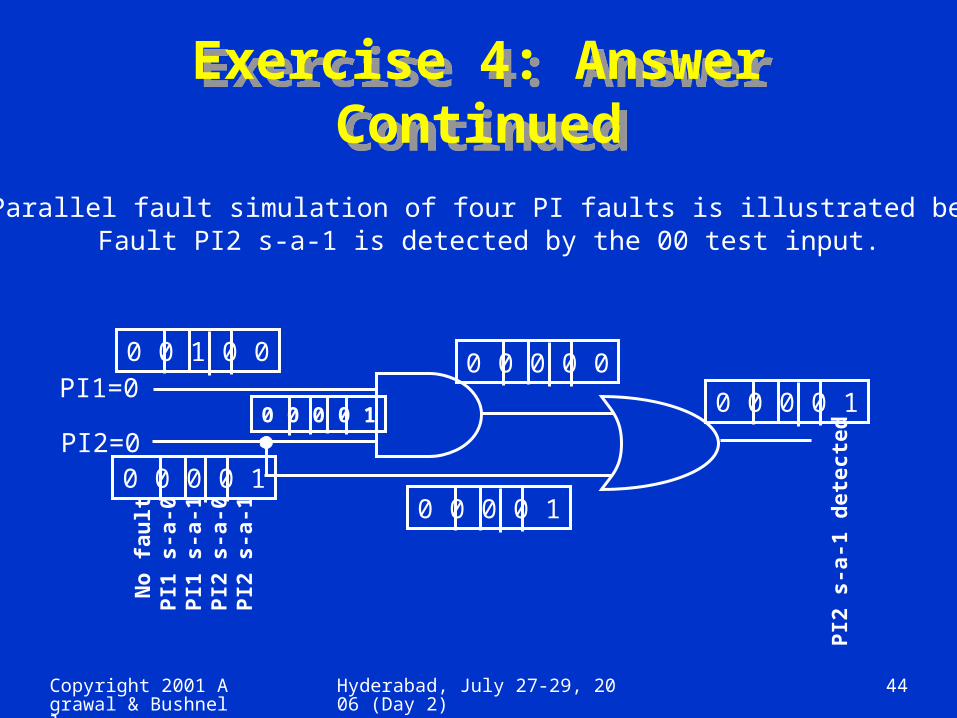
Exercise 4: Answer Continued
Exercise 4: Answer Continued
PI1=0
PI2=0
0 0 1 0 0
0 0 0 0 10 0 0 0 1
0 0 0 0 0
0 0 0 0 1 0 0 0 0 1
No
fau
ltP
I1 s
-a-0
PI1
s-a
-1P
I2 s
-a-0
PI2
s-a
-1
PI2
s-a
-1 d
etec
ted
■ Parallel fault simulation of four PI faults is illustrated below.Fault PI2 s-a-1 is detected by the 00 test input.

Copyright 2001 Agrawal & Bushnell
Hyderabad, July 27-29, 2006 (Day 2) 45
Timing and Delay TestsTiming and Delay Tests

Copyright 2001 Agrawal & Bushnell
Hyderabad, July 27-29, 2006 (Day 2) 46
Delay Test DefinitionDelay Test Definition
A circuit that passes delay test must produce correct outputs when inputs are applied and outputs observed with specified timing.
For a combinational or synchronous sequential circuit, delay test verifies the limits of delay in combinational logic.
Delay test problem for asynchronous circuits is complex and not well understood.
Copyright 2001 Agrawal & Bushnell
Hyderabad, July 27-29, 2006 (Day 2) 47
Digital Circuit TimingDigital Circuit Timing
Inp
uts
Ou
tpu
ts
time
Transientregion
Clock period
Comb.logic
OutputObservation
instant
InputSignal
changes
SynchronizedWith clock
Copyright 2001 Agrawal & Bushnell
Hyderabad, July 27-29, 2006 (Day 2) 48
Circuit DelaysCircuit Delays Switching or inertial delay is the interval between input
change and output change of a gate: Depends on input capacitance, device (transistor)
characteristics and output capacitance of gate. Also depends on input rise or fall times and states of other
inputs (second-order effects). Approximation: fixed rise and fall delays (or min-max delay
range, or single fixed delay) for gate output. Propagation or interconnect delay is the time a transition
takes to travel between gates: Depends on transmission line effects (distributed R, L, C
parameters, length and loading) of routing paths. Approximation: modeled as lumped delays for gate inputs.
See logic simulation for timing models.
Copyright 2001 Agrawal & Bushnell
Hyderabad, July 27-29, 2006 (Day 2) 49
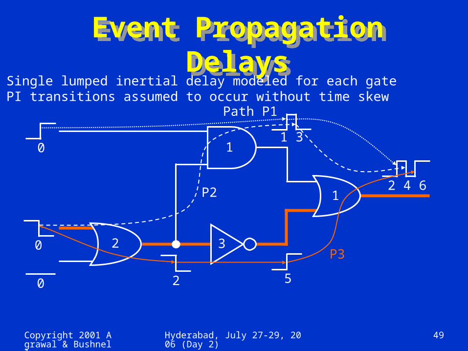
Event Propagation Delays
Event Propagation Delays
2 4 61
1 3
5
3
10
0
0
2
2
Path P1
P2
P3
Single lumped inertial delay modeled for each gatePI transitions assumed to occur without time skew

Copyright 2001 Agrawal & Bushnell
Hyderabad, July 27-29, 2006 (Day 2) 50
Delay Test Generation Problem: Variations in CMOS
Delays
Delay Test Generation Problem: Variations in CMOS
Delays Switching delays in CMOS
greatly depend on the off path signals and internal circuit state
Hard to find <V1, V2> to ensure worst case conditions for signal propagation along a path.
Often this worst case test vector pair can be different for the same circuit depending on fabrication parameters
output
C
A
B
C
BA

Copyright 2001 Agrawal & Bushnell
Hyderabad, July 27-29, 2006 (Day 2) 51
Circuit OutputsCircuit Outputs Each path can potentially produce one signal transition
at the output. The location of an output transition in time is determined
by the delay of the path.
Initial value
Initial value
Final value
Final value
Clock period
Fast transitions Slow transitions
time

Copyright 2001 Agrawal & Bushnell
Hyderabad, July 27-29, 2006 (Day 2) 52
The Transition Delay Fault (TDF) model
The Transition Delay Fault (TDF) model
Assumes a single localized gross delay fault at some node
Faulty node is either slow-to-rise or slow-to- fall For an N node circuit, 2N faults in the fault list Tested by 2-vector test <V1, V2> where the vector
pair is selected to cause a rising (falling) transition at the node to test for a slow-to-rise (slow-to-fall) fault; also V2 is a stuck-at-0 (stuck-at-1) test for the node
Copyright 2001 Agrawal & Bushnell
Hyderabad, July 27-29, 2006 (Day 2) 53
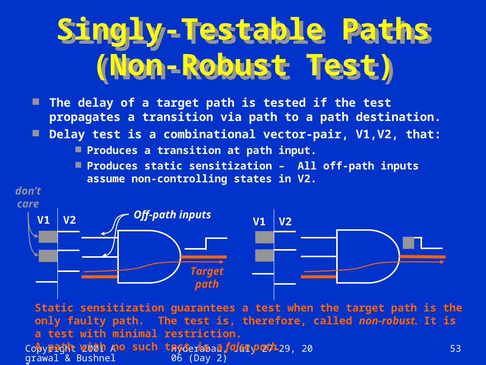
Singly-Testable Paths(Non-Robust Test)
Singly-Testable Paths(Non-Robust Test)
The delay of a target path is tested if the test propagates a transition via path to a path destination.
Delay test is a combinational vector-pair, V1,V2, that: Produces a transition at path input. Produces static sensitization – All off-path inputs assume
non-controlling states in V2.
V1 V2 V1 V2
Static sensitization guarantees a test when the target path is the only faulty path. The test is, therefore, called non-robust. It is a test with minimal restriction.A path with no such test is a false path.
Targetpath
Off-path inputs
don’tcare

Copyright 2001 Agrawal & Bushnell
Hyderabad, July 27-29, 2006 (Day 2) 54
Robust TestRobust Test A robust test guarantees the detection of a delay fault
of the target path, irrespective of delay faults on other paths.
A robust test is a combinational vector-pair, V1, V2, that satisfies following conditions:
Produce real events (different steady-state values for V1 and V2) on all on-path signals.
All on-path signals must have controlling events arriving via the target path.
A robust test is also a non-robust test. Concept of robust test is general – robust tests for
other fault models can be defined.

Copyright 2001 Agrawal & Bushnell
Hyderabad, July 27-29, 2006 (Day 2) 55
Robust Test ConditionsRobust Test Conditions
Real events on target path. Controlling events via target path.
V1 V2 V1 V2
V1 V2
V1 V2
V1 V2
V1 V2
U1
U1
U1/R1
S1
U0/F0
S1
U0
U0
U0/F0
U1/R1
U1/R1
U1/R1U0/F0
U0/F0
S0
S0
Copyright 2001 Agrawal & Bushnell
Hyderabad, July 27-29, 2006 (Day 2) 56
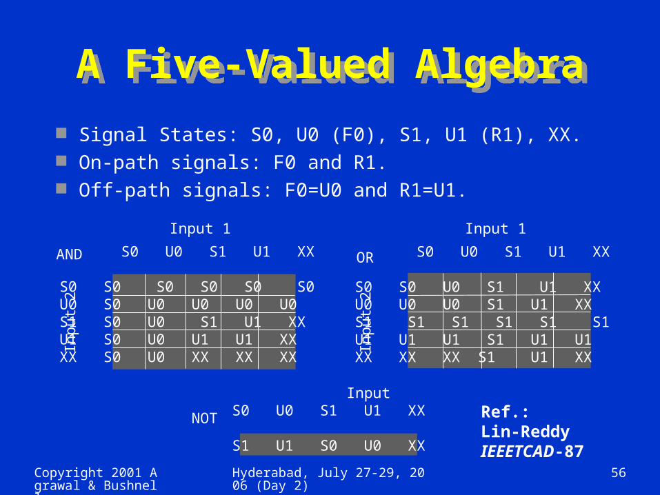
A Five-Valued AlgebraA Five-Valued Algebra
Signal States: S0, U0 (F0), S1, U1 (R1), XX. On-path signals: F0 and R1. Off-path signals: F0=U0 and R1=U1.
S0 U0 S1 U1 XX
S0 S0 S0 S0 S0 S0U0 S0 U0 U0 U0 U0S1 S0 U0 S1 U1 XXU1 S0 U0 U1 U1 XXXX S0 U0 XX XX XX
Input 1
Input
2
S0 U0 S1 U1 XX
S0 S0 U0 S1 U1 XXU0 U0 U0 S1 U1 XXS1 S1 S1 S1 S1 S1U1 U1 U1 S1 U1 U1XX XX XX S1 U1 XX
Input 1
Input
2
InputS0 U0 S1 U1 XX
S1 U1 S0 U0 XX
AND OR
NOT Ref.:Lin-ReddyIEEETCAD-87

Copyright 2001 Agrawal & Bushnell
Hyderabad, July 27-29, 2006 (Day 2) 57
Robust Test GenerationRobust Test Generation
R1
S0U0
R1
XX S0
U0
F0
U0
Path P3
Test for ↓ P3 – falling transition through path P3: Steps A through E
F0
XX
A. Place F0 at path origin
B. Propagate F0 through OR gate; also propagates as R1 through NOT gate
C. F0 interpreted as U0; propagates through AND gate
D. Change off-path input to S0 to Propagate R1 through OR gate
E. Set input of AND gate to S0 to justify S0 at output
Robust Test:S0, F0, U0
Copyright 2001 Agrawal & Bushnell
Hyderabad, July 27-29, 2006 (Day 2) 58
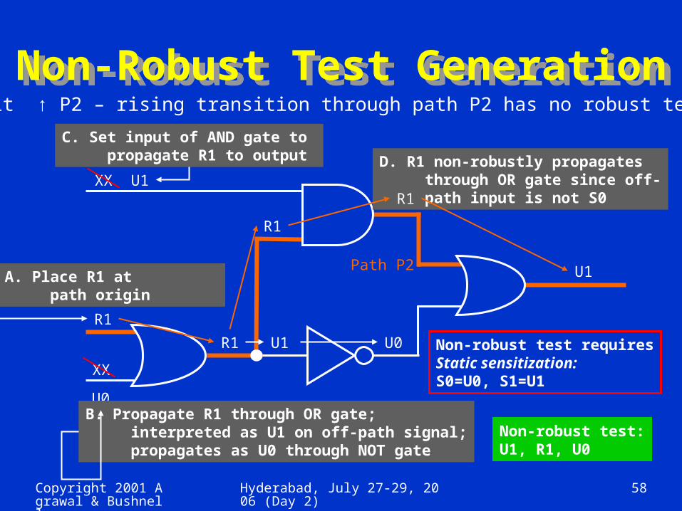
Non-Robust Test GenerationNon-Robust Test Generation
U1
U0
XX U1
U0
R1
R1
Path P2
Fault ↑ P2 – rising transition through path P2 has no robust test.
R1
XX
A. Place R1 at path origin
B. Propagate R1 through OR gate; interpreted as U1 on off-path signal; propagates as U0 through NOT gate
D. R1 non-robustly propagates through OR gate since off- path input is not S0
C. Set input of AND gate to propagate R1 to output
Non-robust test:U1, R1, U0
U1 Non-robust test requiresStatic sensitization:S0=U0, S1=U1
R1

Copyright 2001 Agrawal & Bushnell
Hyderabad, July 27-29, 2006 (Day 2) 59
Path-Delay Faults (PDF)Path-Delay Faults (PDF) Two PDFs (rising and falling transitions) for each physical path. Total number of paths is an exponential function of gates. Critical
paths, identified by static timing analysis (e.g., Primetime from Synopsys), must be tested.
PDF tests are delay-independent. Robust tests are preferred, but some paths have only non-robust tests.
Three types of PDFs (Gharaybeh, et al., JETTA (11), 1997): Singly-testable PDF – has a non-robust or robust test. Multiply-testable PDF – a set of singly untestable faults that has a
non-robust or robust test. Also known as functionally testable PDF.
Untestable PDF – a PDF that is neither singly nor multiply testable. A singly-testable PDF has at least one single-input change (SIC)
non-robust test.
Copyright 2001 Agrawal & Bushnell
Hyderabad, July 27-29, 2006 (Day 2) 60
Other Delay Fault Models
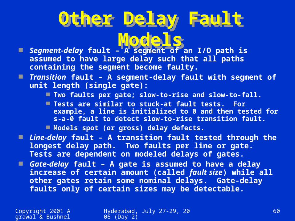
Other Delay Fault Models
Segment-delay fault – A segment of an I/O path is assumed to have large delay such that all paths containing the segment become faulty.
Transition fault – A segment-delay fault with segment of unit length (single gate):
Two faults per gate; slow-to-rise and slow-to-fall. Tests are similar to stuck-at fault tests. For example, a line is
initialized to 0 and then tested for s-a-0 fault to detect slow-to-rise transition fault.
Models spot (or gross) delay defects. Line-delay fault – A transition fault tested through the longest
delay path. Two faults per line or gate. Tests are dependent on modeled delays of gates.
Gate-delay fault – A gate is assumed to have a delay increase of certain amount (called fault size) while all other gates retain some nominal delays. Gate-delay faults only of certain sizes may be detectable.

Copyright 2001 Agrawal & Bushnell
Hyderabad, July 27-29, 2006 (Day 2) 61
At-Speed TestAt-Speed Test At-speed test means application of test vectors at the rated-
clock speed. Two methods of at-speed test. External test:
Vectors may test one or more functional critical (longest delay) paths and a large percentage (~100%) of transition faults.
High-speed testers are expensive. Built-in self-test (BIST):
Hardware-generated random vectors applied to combinational or sequential logic.
Only clock is externally supplied. Non-functional paths that are longer than the functional
critical path can be activated and cause a good circuit to fail.
Some circuits have initialization problem.

Copyright 2001 Agrawal & Bushnell
Hyderabad, July 27-29, 2006 (Day 2) 62
Timing Design & Delay TestTiming Design & Delay Test
Timing simulation: Critical paths are identified by static (vector-less) timing
analysis tools like Primetime (Synopsys). Timing or circuit-level simulation using designer-generated
functional vectors verifies the design. Layout optimization: Critical path data are used in
placement and routing. Delay parameter extraction, timing simulation and layout are repeated for iterative improvement.
Testing: Some form of at-speed test is necessary. PDFs for critical paths and all transition faults are tested.

Copyright 2001 Agrawal & Bushnell
Hyderabad, July 27-29, 2006 (Day 2) 63
Even if good delay test vectors can be generated, scan can only support very limited two vector test patterns launch-on-shift (“skewed load”) launch-on-capture (“broad side”)
Many desired delay timing tests may be impossible to apply in a scan environment.
Problems with Delay Test Application in a Scan
Environment
Problems with Delay Test Application in a Scan
Environment

Copyright 2001 Agrawal & Bushnell
Hyderabad, July 27-29, 2006 (Day 2) 64
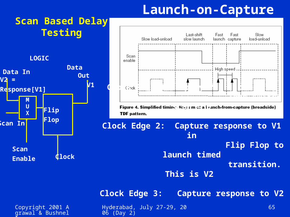
MUX
Flip
Flop
Data In
Scan
Enable
Scan In
Data Out
Clock
LOGIC
Launch-on-Shift
Launch-on-Shift
Clock Edge 1: Launch V2 (scan = 1)
Then switch scan = 0
Clock Edge 2: Capture response to V1 → V2 change in Flip Flop
Scan Based Delay Testing
V1
V2
Copyright 2001 Agrawal & Bushnell
Hyderabad, July 27-29, 2006 (Day 2) 65
MUX
Flip
Flop
Data In
Scan
Enable
Scan In
Data Out
Clock
LOGIC
Launch-on-Capture
Scan Based Delay Testing
Clock Edge 1: Apply V1 (scan = 1) Then switch scan = 0
Clock Edge 2: Capture response to V1 in Flip Flop to launch timed
transition. This is V2
Clock Edge 3: Capture response to V2
V1V2 =
Response[V1]
Copyright 2001 Agrawal & Bushnell
Hyderabad, July 27-29, 2006 (Day 2) 66
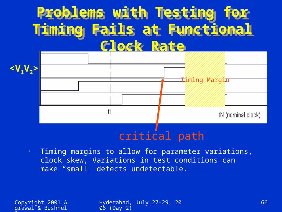
Problems with Testing for Timing Fails at Functional
Clock Rate
Problems with Testing for Timing Fails at Functional
Clock Rate
• Timing margins to allow for parameter variations, clock skew, variations in test conditions can make “small” defects undetectable.
<V1V2>
critical path
Timing Margin

Copyright 2001 Agrawal & Bushnell
Hyderabad, July 27-29, 2006 (Day 2) 67
minVDD Testing minVDD Testing
minVDD is found by repeatedly running the test vectors at different VDD voltages and performing a binary search until the failing voltage is identified within desired accuracy
Since binary searches on full vector sets can be expensive, methods have been developed to work with reduced test sets.

Copyright 2001 Agrawal & Bushnell
Hyderabad, July 27-29, 2006 (Day 2) 68
MinVDD vs Device Speed Two different lots showing min VDD outliers and lot-to-lot
intrinsic variation.
MinVDD vs Device Speed Two different lots showing min VDD outliers and lot-to-lot
intrinsic variation.

Copyright 2001 Agrawal & Bushnell
Hyderabad, July 27-29, 2006 (Day 2) 69
minVDD TestingminVDD Testing
Minimum VDD results for different functional tests
clearly showing min VDD outliers (circled)
Copyright 2001 Agrawal & Bushnell
Hyderabad, July 27-29, 2006 (Day 2) 70
Fmax Testing Fmax Testing
Fmax Testing finds the highest clock rate for which a circuit passes a given (TDF) test set
A binary search using repeated applications of the test set is performed to obtain Fmax
Again an abnormal Fmax value compared to neighbors indicates a defect that may cause a functional or reliability failure in the field

Copyright 2001 Agrawal & Bushnell
Hyderabad, July 27-29, 2006 (Day 2) 71
Fmax TestingFmax Testing
Fmax for TDF pattern for 32 parts that passdc tests but fail system level tests
Operational Clock
Intrinsic Clock

Copyright 2001 Agrawal & Bushnell
Hyderabad, July 27-29, 2006 (Day 2) 72
Stress TestingStress Testing ICs also experience significant early life or “infant
mortality” failures (0.2-2%)
Infant mortality results from latent manufacturing flaws that are undetectable at initial wafer probe testing
Important to screen out such failures using accelerated life cycle or stress tests
Burn-in tests exercise circuits at elevated voltages and temperatures for a few hours up to a few days in temperature controlled burn-in “ovens”

Copyright 2001 Agrawal & Bushnell
Hyderabad, July 27-29, 2006 (Day 2) 73
Screening for Burn-inMinimization
Screening for Burn-inMinimization
High end circuits have nanometer feature sizes and operate on low voltages
Stress voltages and temperatures must be carefully (individually) controlled to avoid damaging the circuits >> expensive ovens
Needed burn-in times are growing because voltage/temperature stress levels can only be marginally increased from the nominal
Some defect types do not accelerate in burn-in
Statistical outlier screening is now being also used to minimize burn-in

Copyright 2001 Agrawal & Bushnell
Hyderabad, July 27-29, 2006 (Day 2) 74
SummarySummary Path-delay fault (PDF) models distributed delay defects. It verifies
the timing performance of a manufactured circuit. Transition fault models spot delay defects and is testable by
modified stuck-at fault tests. Variable-clock method can test delay faults but the test time can be
long. Critical paths of non-scan sequential circuits can be effectively
tested by rated-clock tests. Delay test methods (including BIST) for non-scan sequential
circuits using slow ATE require investigation: Suppression of non-functional path activation in BIST. Difficulty of rated-clock PDF test generation. Long sequences of variable-clock tests.

Copyright 2001 Agrawal & Bushnell
Hyderabad, July 27-29, 2006 (Day 2) 75
IDDQ Current TestingIDDQ Current Testing
Copyright 2001 Agrawal & Bushnell
Hyderabad, July 27-29, 2006 (Day 2) 76
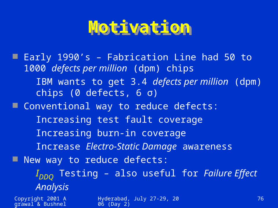
MotivationMotivation
Early 1990’s – Fabrication Line had 50 to 1000 defects per million (dpm) chips IBM wants to get 3.4 defects per million (dpm) chips (0
defects, 6 σ) Conventional way to reduce defects:
Increasing test fault coverage Increasing burn-in coverage Increase Electro-Static Damage awareness
New way to reduce defects:
IDDQ Testing – also useful for Failure Effect Analysis
Copyright 2001 Agrawal & Bushnell
Hyderabad, July 27-29, 2006 (Day 2) 77
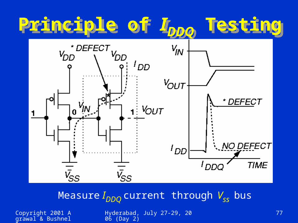
Principle of IDDQ TestingPrinciple of IDDQ Testing
Measure IDDQ current through Vss bus
Copyright 2001 Agrawal & Bushnell
Hyderabad, July 27-29, 2006 (Day 2) 78
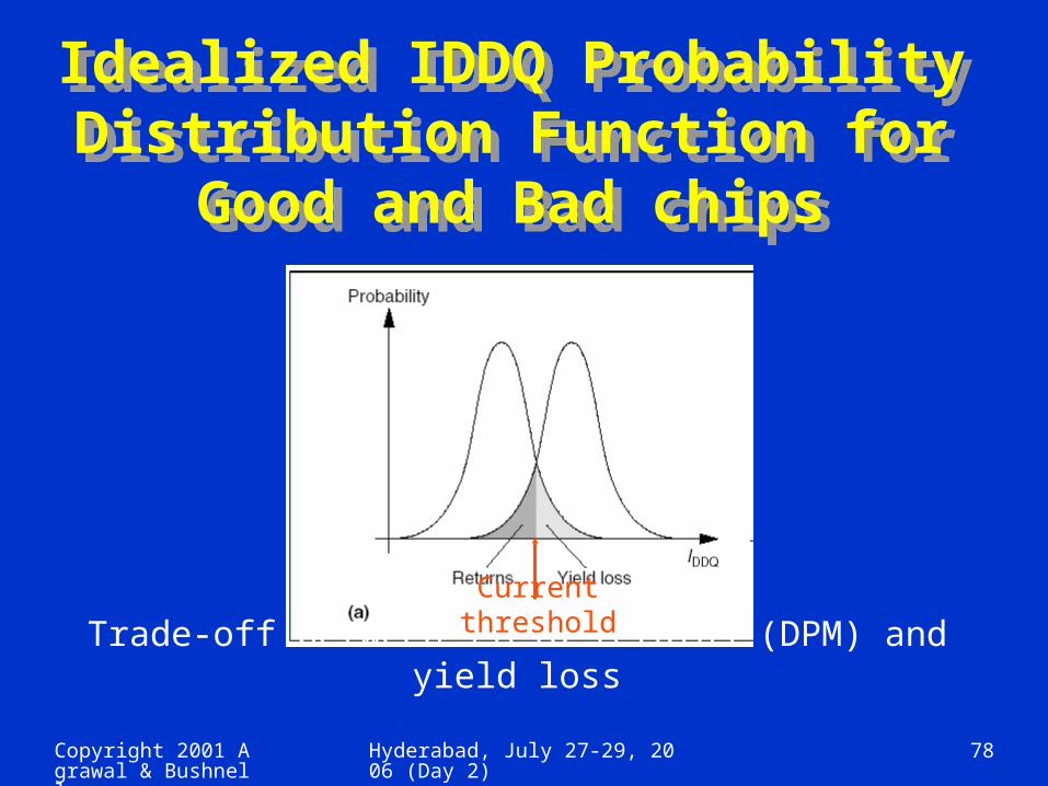
Trade-off between field returns (DPM) and yield loss
Current threshold
Idealized IDDQ Probability Distribution Function for
Good and Bad chips
Idealized IDDQ Probability Distribution Function for
Good and Bad chips

Copyright 2001 Agrawal & Bushnell
Hyderabad, July 27-29, 2006 (Day 2) 79
Stuck-at Faults Detected by IDDQ Tests
Stuck-at Faults Detected by IDDQ Tests
Bridging faults with stuck-at fault behavior Levi – Bridging of a logic node to VDD or VSS – few of
these Transistor gate oxide short of 1 kΩ to 5 kΩ
Floating MOSFET gate defects – do not fully turn off transistor
Copyright 2001 Agrawal & Bushnell
Hyderabad, July 27-29, 2006 (Day 2) 80
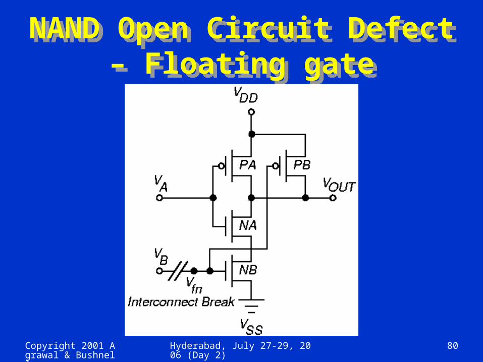
NAND Open Circuit Defect – Floating gate
NAND Open Circuit Defect – Floating gate

Copyright 2001 Agrawal & Bushnell
Hyderabad, July 27-29, 2006 (Day 2) 81
Floating Gate DefectsFloating Gate Defects
Small break in logic gate inputs (100 – 200 Angstroms) lets wires couple by electron tunneling Delay fault and IDDQ fault
Large open results in stuck-at fault – not detectable by IDDQ test
If Vtn < Vfn < VDD - | Vtp | then detectable by IDDQ
test

Copyright 2001 Agrawal & Bushnell
Hyderabad, July 27-29, 2006 (Day 2) 82
Delay FaultsDelay Faults
Most random CMOS defects cause a timing delay fault, not catastrophic failure
Many delay faults detected by IDDQ test – late
switching of logic gates keeps IDDQ elevated
Delay faults not detected by IDDQ test
Resistive via fault in interconnect Increased transistor threshold voltage fault

Copyright 2001 Agrawal & Bushnell
Hyderabad, July 27-29, 2006 (Day 2) 83
Leakage FaultsLeakage Faults
Gate oxide shorts cause leaks between gate & source or
gate & drain
Mao and Gulati leakage fault model:
Leakage path flags: fGS, fGD, fSD, fBS, fBD, fBG
G = gate, S = source, D = drain, B = bulk
Assume that short does not change logic values
Copyright 2001 Agrawal & Bushnell
Hyderabad, July 27-29, 2006 (Day 2) 84
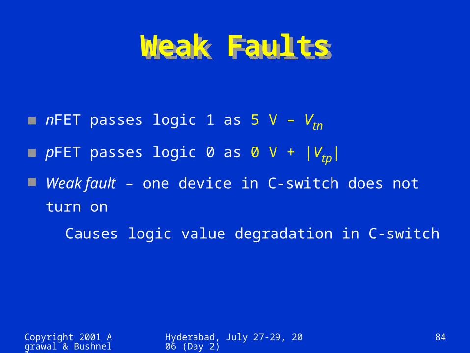
Weak FaultsWeak Faults
nFET passes logic 1 as 5 V – Vtn
pFET passes logic 0 as 0 V + |Vtp|
Weak fault – one device in C-switch does not turn on
Causes logic value degradation in C-switch

Copyright 2001 Agrawal & Bushnell
Hyderabad, July 27-29, 2006 (Day 2) 85
Gate Oxide ShortGate Oxide Short

Copyright 2001 Agrawal & Bushnell
Hyderabad, July 27-29, 2006 (Day 2) 86
Instrumentation Problems
Instrumentation Problems
Need to measure < 1 μA current at clock > 10 kHz Off-chip IDDQ measurements degraded
Pulse width of CMOS IC transient current Impedance loading of tester probe Current leakages in tester High noise of tester load board
Much slower rate of current measurement than voltage measurement

Copyright 2001 Agrawal & Bushnell
Hyderabad, July 27-29, 2006 (Day 2) 87
Sematech StudySematech Study IBM Graphics controller chip – CMOS ASIC, 166,000
standard cells 0.8 mm static CMOS, 0.45 μm Lines (Leff), 40 to 50 MHz
Clock, 3 metal layers, 2 clocks Full boundary scan on chip Tests:
Scan flush – 25 ns latch-to-latch delay test 99.7 % scan-based stuck-at faults (slow 400 ns rate) 52 % SAF coverage functional tests (manually created) 90 % transition delay fault coverage tests
96 % pseudo-stuck-at fault cov. IDDQ Tests

Copyright 2001 Agrawal & Bushnell
Hyderabad, July 27-29, 2006 (Day 2) 88
Sematech ResultsSematech Results Test process: Wafer Test → Package Test →
Burn-In & Retest → Characterize & Failure Analysis Data for devices failing some, but not all, tests.
passpassfailfail
pass
146
52pass
pass601
36fail
fail1463
3413
1251pass
fail718
fail
passfail
passfail
Sca
n-b
ased
Stu
ck-a
t IDDQ (5 μA limit)
Functional
Sca
n-b
ased
del
ay

Copyright 2001 Agrawal & Bushnell
Hyderabad, July 27-29, 2006 (Day 2) 89
Sematech ConclusionsSematech Conclusions
Hard to find point differentiating good and bad devices for IDDQ & delay tests
High # passed functional test, failed all others High # passed all tests, failed IDDQ > 5 μA Large # passed stuck-at and functional tests
Failed delay & IDDQ tests Large # failed stuck-at & delay tests
Passed IDDQ & functional tests Delay test caught delays in chips at higher Temperature
burn-in – chips passed at lower T.

Copyright 2001 Agrawal & Bushnell
Hyderabad, July 27-29, 2006 (Day 2) 90
Limitations of IDDQ TestingLimitations of IDDQ Testing
Sub-micron technologies have increased leakage currents Transistor sub-threshold conduction
Harder to find IDDQ threshold separating good and
bad chips IDDQ tests work:
When average defect-induced current greater than average good IC current
Small variation in IDDQ over test sequence and
between chips Now less likely to obtain two conditions

Copyright 2001 Agrawal & Bushnell
Hyderabad, July 27-29, 2006 (Day 2) 91
Current Limit SettingCurrent Limit Setting Should try to get it < 1 μA Histogram for 32 bit microprocessor

Copyright 2001 Agrawal & Bushnell
Hyderabad, July 27-29, 2006 (Day 2) 92
Failure Distribution in Hewlett-Packard ChipFailure Distribution in Hewlett-Packard Chip

Copyright 2001 Agrawal & Bushnell
Hyderabad, July 27-29, 2006 (Day 2) 93
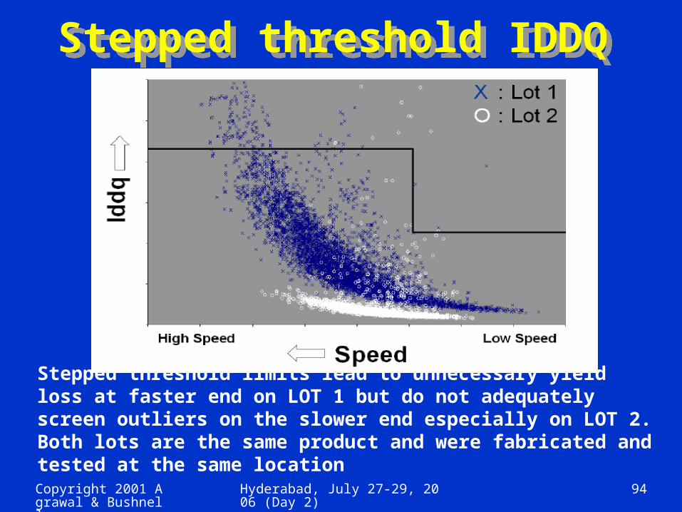
Three processing lots of IDDQ data for a single product.
The Problem with using a single IDDQ threshold
The Problem with using a single IDDQ threshold
Copyright 2001 Agrawal & Bushnell
Hyderabad, July 27-29, 2006 (Day 2) 94
Stepped threshold limits lead to unnecessary yield loss at faster end on LOT 1 but do not adequately screen outliers on the slower end especially on LOT 2. Both lots are the same product and were fabricated and tested at the same location
Stepped threshold IDDQStepped threshold IDDQ

Copyright 2001 Agrawal & Bushnell
Hyderabad, July 27-29, 2006 (Day 2) 95
Single threshold IDDQSingle threshold IDDQ
Excessive yield loss is observed at wafer edge due to single threshold IDDQ limits
Copyright 2001 Agrawal & Bushnell
Hyderabad, July 27-29, 2006 (Day 2) 96
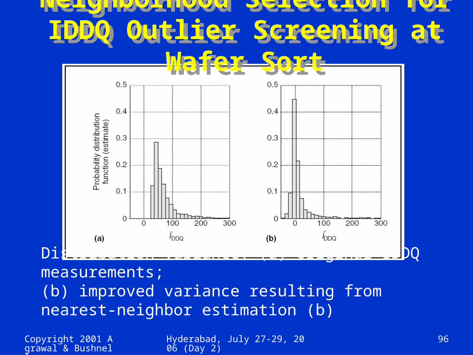
Distribution variance: (a) original IDDQ measurements;(b) improved variance resulting from nearest-neighbor estimation (b)
Neighborhood Selection for IDDQ Outlier Screening at
Wafer Sort
Neighborhood Selection for IDDQ Outlier Screening at
Wafer Sort

Copyright 2001 Agrawal & Bushnell
Hyderabad, July 27-29, 2006 (Day 2) 97
% Functional Failures After 100 Hours Life Test
% Functional Failures After 100 Hours Life Test
Work of McEuen at Ford Microelectronics
Copyright 2001 Agrawal & Bushnell
Hyderabad, July 27-29, 2006 (Day 2) 98
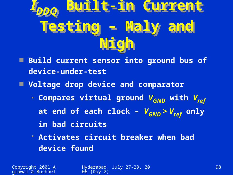
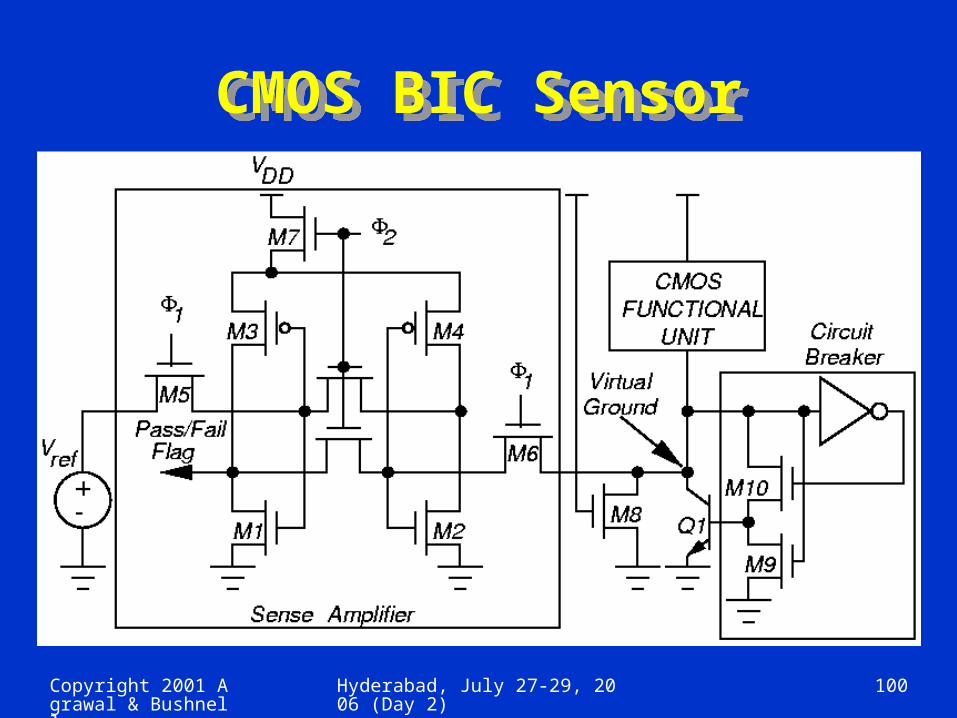
IDDQ Built-in Current Testing – Maly and Nigh
IDDQ Built-in Current Testing – Maly and Nigh
Build current sensor into ground bus of device-
under-test
Voltage drop device and comparator
Compares virtual ground VGND with Vref at end
of each clock – VGND > Vref only in bad circuits
Activates circuit breaker when bad device
found

Copyright 2001 Agrawal & Bushnell
Hyderabad, July 27-29, 2006 (Day 2) 99
Conceptual BIC SensorConceptual BIC Sensor
Copyright 2001 Agrawal & Bushnell
Hyderabad, July 27-29, 2006 (Day 2) 100
CMOS BIC SensorCMOS BIC Sensor

Copyright 2001 Agrawal & Bushnell
Hyderabad, July 27-29, 2006 (Day 2) 101
SummarySummary IDDQ tests improve reliability, find defects causing:
Delay, bridging, weak faults Chips damaged by electro-static discharge
No natural breakpoint for current threshold Get continuous distribution – bimodal would be better
Conclusion: now need stuck-fault, IDDQ, and delay fault
testing combined
Still uncertain whether IDDQ tests will remain useful as
chip feature sizes shrink further
Related Documents