PJ5KPS User & Technical Manual Manifactured by Italy

Welcome message from author
This document is posted to help you gain knowledge. Please leave a comment to let me know what you think about it! Share it to your friends and learn new things together.
Transcript

PJ5KPS
User & TechnicalManual
Manifactured by Italy

PJ5KPS - Use and maintenance manualVersione 1.5
© Copyright 2003-2006R.V.R. Elettronica SpAVia del Fonditore 2/2c - 40138 - Bologna (Italia)Telefono: +39 051 6010506Fax: +39 051 6011104Email: [email protected]: www.rvr.it
All rights reservedPrinted and bound in Italy. No part of this manual may be reproduced,memorized or transmitted in any form or by any means, eletronic ormechanic, including photocopying, recording or by any informationstorage and retrieval system, whithout the permission of the copyrightowner.
Docum ent History Date Version Reason Editor 30/01/02 1.0 First Version D. Canazza
24/10/02 1.1 General Revision. New form at (PageM aker). Insert of chapter 8. Technical appendix integrated. D. Canazza
18/11/02 1.2
Stand-by functions update. Power-on procedure corrections. New section chap.8 I/O interface board. New schem atic version of W iring diagram and PSSW 5040
D. Canazza
19/12/03 1.3 Insert of chapter 9. Technical Appendix upgradated. J. Berti 31/10/05 1.4 SLPW RM TRPJ5 Board Upgrade J. Berti 08/02/06 1.5 SL042M T1001 and SL042RF1001 board upgrading J. Berti

Notification of intended purpose and limitations of product useThis product is a FM transmitter intended for FM audio broadcasting. It utilisesoperating frequencies not harmonised in the intended countries of use.The user must obtain a license before using the product in intended country ofuse. Ensure respective country licensing requirements are complied with.Limitations of use can apply in respect of operating freuency, transmitter powerand/or channel spacing.
Declaration of ConformityHereby, R.V.R. Elettronica SpA, declares that this FM transmitter is incompliance with the essential requirements and other relevant provisions ofDirective 1999/5/EC.

This page intentionally left blank
PJ5KPS
iUser & Technical Manual Rev. 1.5- 08/02/06
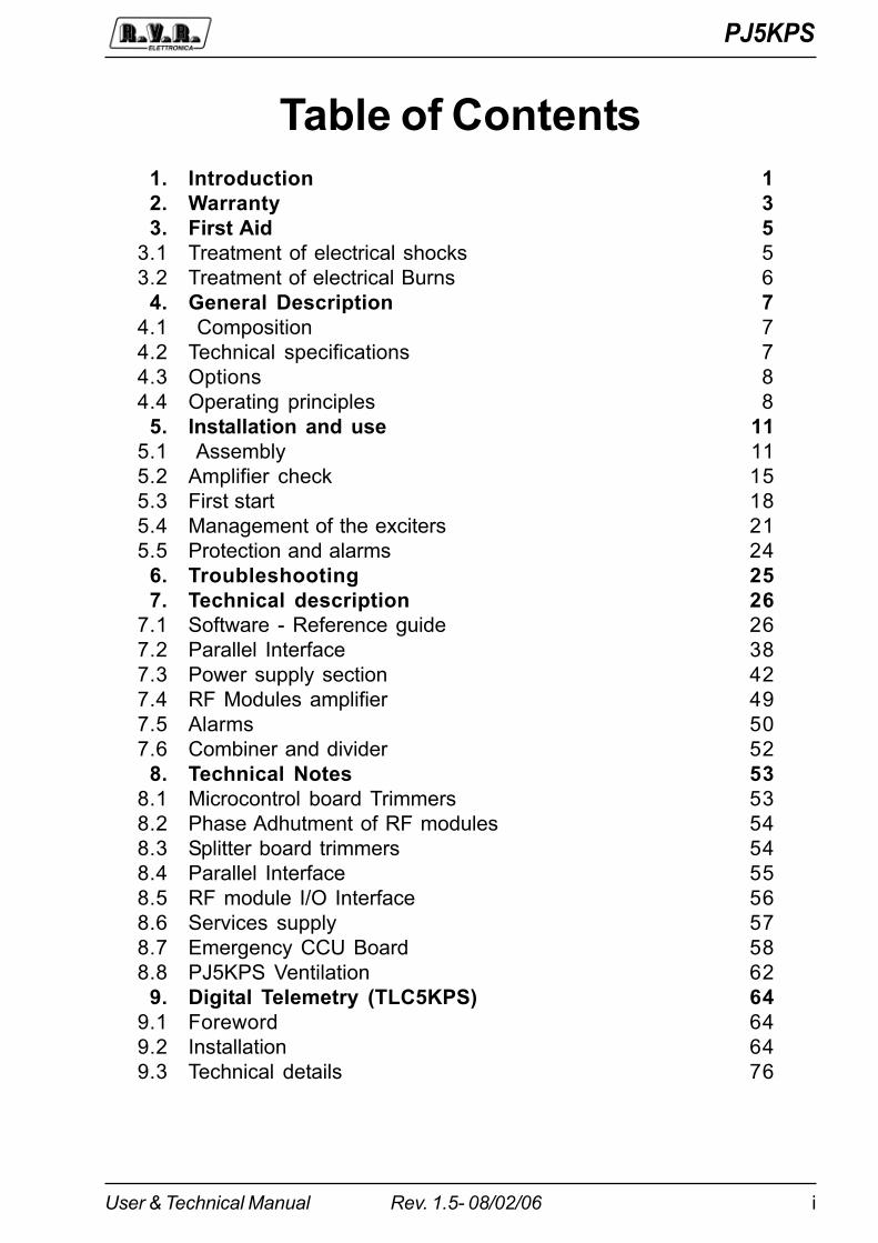
Table of Contents1. Introduction 12. Warranty 33. First Aid 5
3.1 Treatment of electrical shocks 53.2 Treatment of electrical Burns 6
4. General Description 74.1 Composition 74.2 Technical specifications 74.3 Options 84.4 Operating principles 8
5. Installation and use 115.1 Assembly 115.2 Amplifier check 155.3 First start 185.4 Management of the exciters 215.5 Protection and alarms 24
6. Troubleshooting 257. Technical description 26
7.1 Software - Reference guide 267.2 Parallel Interface 387.3 Power supply section 427.4 RF Modules amplifier 497.5 Alarms 507.6 Combiner and divider 52
8. Technical Notes 538.1 Microcontrol board Trimmers 538.2 Phase Adhutment of RF modules 548.3 Splitter board trimmers 548.4 Parallel Interface 558.5 RF module I/O Interface 568.6 Services supply 578.7 Emergency CCU Board 588.8 PJ5KPS Ventilation 62
9. Digital Telemetry (TLC5KPS) 649.1 Foreword 649.2 Installation 649.3 Technical details 76

PJ5KPS
ii User & Technical ManualRev. 1.5- 08/02/06
This page was intentionally left blank
PJ5KPS
1 / 80User & Technical Manual Rev. 1.5 - 08/02/06
1. IntroductionThis manual describes the PJ5KPS, a solid-state RF amplifier designed forfrequency modulation sound broadcasting, manufactured by R.V.R. Elettronica.The PJ5KPS amplifier constitutes the end power section for FM transmitters fittedwith different possible configurations. A control system for the exciters is built intothe machine so that in order to have a system with redundant exciters, all thatneeds to be done is to include two exciters in the transmitter such as, for example,the PTX30LCD exciters made by R.V.R. Elettronica.
The manual is structured as follows:
� Chapter 1: Presentation of the manual
� Chapter 2: Warranty conditions
� Chapter 3: Safety recommendations
� Chapter 4: Description of the machine and its operating principles
� Chapter 5: Guide for installation and use
� Chapter 6: Most frequent troubleshooting cases on starting up the machine
� Chapter 7: In-depth description of the operation of the modules of the apparatus.This chapter also contains the description of the pin configuration of theconnectors and explains how to use the control unit menus, item by item.
� Chapter 8: technical notes.
� Appendix: It contains all the design details (wiring diagrams, assembly plans,etc.) of the PJ5KPS.
This manual is written as a general guide for those having previous knowledgeand experience with this kind of equipment, well conscious of the risks connectedwith the operation of electrical equipment.
It is not intended to contain a complete statement of all safety rules which shouldbe observed by personnel in using this or other electronic equipment.
The installation, use and maintenance of this piece of equipment involve risksboth for the personnel performing them and for the device itself, that shall be usedonly by trained personnel.
R.V.R. Elettronica SpA doesn�t assume responsibility for injury or damage resultingfrom improper procedures or practices by untrained/unqualified personnel in thehandling of this unit.
Please observe all local codes and fire protection standards in the operations ofthis unit.
WARNING: always disconnect power before opening covers or removing anypart of this unit.Use appropriate grounding procedures to short out capacitors and high voltage
PJ5KPS
2 / 80 User & Technical ManualRev. 1.5 - 08/02/06
points before servicing.
WARNING: this device can irradiate radio frequency waves, and if it�s not installedfollowing the instructions contained in the manual and local regulations it couldgenerate interferences in radio communications.This is a "CLASS A" equipment. In a residential place this equipment can causehash. In this case can be requested to user to take the necessary measures.
R.V.R. Elettronica SpA reserves the right to modify the design and/or the technicalspecifications of the product and this manual without notice.
PJ5KPS
3 / 80User & Technical Manual Rev. 1.5 - 08/02/06
2. WarrantyAny product of R.V.R. Elettronica is covered by a 24 (twentyfour) month warranty.
For components like tubes for power amplifiers, the original manufacturer�s warrantyapplies.R.V.R. Elettronica SpA extends to the original end-user purchaser allmanufacturers warranties which are transferrable and all claims are to be madedirectly to R.V.R. per indicated procedures.
Warranty shall not include:
1 danni verificatisi durante la spedizione della macchina alla R.V.R. per eventualiriparazioni;
2 Any unauthorized repair/modification;
3 Incidental/consequential damages as a result of any defect
4 Nominal non-incidental defects
5 Re-shipment costs or insurance of the unit or replacement units/parts
Any damage to the goods must be reported to the carrier in writing on the shipmentreceipt.
Any discrepancy or damage discovered subsequent to delivery, shall be reportedto R.V.R. Elettronica within 5 (five) days from delivery date.
To claim your rights under this warranty, you shold follow this procedure:
1 Contact the dealer or distributor where you purchased the unit. Describe theproblem and, so that a possible easy solution can be detected.
Dealers and Distributors are supplied with all the information about problemsthat may occur and usually they can repair the unit quicker than what themanufacturer could do. Very often installing errors are discovered by dealers.
2 If your dealer cannot help you, contact R.V.R. Elettronica and explain theproblem. If it is decided to return the unit to the factory, R.V.R. Elettronicawill mail you a regular authorization with all the necessary instructions to sendback the goods.
3 When you receive the authorization, you can return the unit. Pack it carefullyfor the shipment, preferably using the original packing and seal the packageperfectly. The customer always assumes the risks of loss (i.e., R.V.R. is neverresponsible for damage or loss), until the package reaches R.V.R. premises.For this reason, we suggest you to insure the goods for the whole value.Shipment must be effected C.I.F. (PREPAID) to the address specified by R.V.R.�sservice manager on the authorization
DO NOT RETURN UNITS WITHOUT OUR AUTHORIZATION AS THEY WILLBE REFUSED
PJ5KPS
4 / 80 User & Technical ManualRev. 1.5 - 08/02/06
4 Be sure to enclose a written technical report where mention all the problems foundand a copy of your original invoice establishing the starting date of the warranty.
Replacement and warranty parts may be ordered from the following address. Besure to include the equipment model and serial number as well as part descriptionand part number.
R.V.R. Elettronica SpAVia del Fonditore, 2/2c40138 BOLOGNAITALYTel. +39 051 6010506
PJ5KPS
5 / 80User & Technical Manual Rev. 1.5 - 08/02/06
3. First AidThe personnel employed in the installation, use and maintenance of the device,shall be familiar with theory and practice of first aid..
3.1 Treatment of electrical shocks
3.1.1 If the victim is not responsive
Follow the A-B-C's of basic life support
� Place victim flat on his backon a hard surface.
� Open airway: lift up neck, push forehead back (Fig. 3-1).
� clear out mouth if necessary and observe for breathing
� if not breathing, begin artificial breathing (Figure 3-2): tilt head, pinch nostrils,make airtight seal, four quick full breaths. Remember mouth to mouthresuscitation must be commenced as soon as possible
Figure 3-1 Figure 3-2
� Check carotid pulse (Fig 3-3); if pulse is absent, begin artificial circulation(Fig. 3-4) depressing sternum (Fig. 3-5)
Figure 3-3 Figure 3-4 Figure 3-5
� In case of only one rescuer, 15 compressions alternated to two breaths.
� If there are two rescuers, the rythm shall be of one brath each 5 compressions.
� Do not interrupt the rythm of compressions when the second person is givingbreath.
� Call for medical assistance as soon as possible.
PJ5KPS
6 / 80 User & Technical ManualRev. 1.5 - 08/02/06
3.1.2 If victim is responsive� Keep them warm
� Keep them as quiet as possible
� Loosen their clothing (a reclining position is recommended)
� Call for medical help as soon as possible
3.2 Treatment of electrical Burns
3.2.1 Extensive burned and broken skin� Cover area with clean sheet or cloth
� Do not break blisters, remove tissue, remove adhered particles of clothing, orapply any salve or ointment.
� Treat victim for shock as required.
� Arrange transportation to a hospital as quickly as possible.
� If arms or legs are affected keep them elevated
If medical help will not be available within an hour and the victim is conscious andnot vomiting, give him a weak solution of salt and soda: 1 level teaspoonful of saltand 1/2 level teaspoonful of baking soda to each quart of water (neither hot orcold). Allow victim to sip slowly about 4 ounces (half a glass) over a period of 15minutes. Discontinue fluid if vomiting occurs
DO NOT give alcohol
3.2.2 Less severe burns� Apply cool (not ice cold) compresses using the cleansed available cloth article.
� Do not break blisters, remove tissue, remove adhered particles of clothing, orapply salve or ointment.
� Apply clean dry dressing if necessary.
� Treat victim for shock as required.
� Arrange transportation to a hospital as quickly as possible
� If arms or legs are affected keep them elevated.
PJ5KPS
7 / 80User & Technical Manual Rev. 1.5 - 08/02/06
4. General DescriptionThe PJ5KPS is a RF amplifier for frequency modulation sound broadcasting. It is afully solid-state apparatus of modern design that uses MOSFET as active componentsin the FM amplifying modules. This chapter briefly describes the machine's mainfeatures.
4.1 Composition
The PJ5KPS amplifier is made up of modules inserted in a 19" rack. The mainmodules are as follows:
� 1 Control unit
� 5 1.2 kW RF amplifier modules
� 1 Control unit
� 1 or 2 Power supply unit carriages
� 1 Splitter/Input RF
The amplifier is supplied complete with all its parts, not really "modules", essentialfor its operation such as the fans for dissipating the heat generated by the machineinside the room and all the accessories for the electrical and RF wiring. As a rule, theamplifier is supplied as a complete transmitter therefore the two FM exciters that itmanages will be provided and connected (a service exciter and a spare exciter).
4.2 Technical specifications
Frequency range 87.5 to 108.0 MHzNominal RF power 5000 WPower supply voltage 380 Three-phase, 3F+NExciting power Max. 30 WConsumption < 9.5 kWPower factor > 0.95
Additional important features of the PJ5KPS are as follows:
� The 1.2 kW amplifying modules are implemented by means of plug-in technology:the individual modules may be removed for performing maintenance operations,for instance, without having to turn off the transmitter. The transmitter keeps workingat reduced power even if the module has been removed. This operation may becarried out without any risk of damaging the module itself, or the amplifier as awhole, thanks to the control system and to the RF connectors, the power supplyand the purposely designed data-exchange. For further information refer to themaintenance section.
� Each module is controlled by a microprocessor-based card that checks andadjusts its operating mode. The resulting data are transmitted to the control unit.
� The control unit manages the changeover of the two exciters both in automaticand manual mode.
PJ5KPS
8 / 80 User & Technical ManualRev. 1.5 - 08/02/06
� The amplifier may be equipped with a dual power supply/rectifier module. Bothmodules operate in this case the configuration is in �hot stand-by� since bothsupply, when operating under normal conditions, half of the current required bythe machine to work. When one module is absent or faulty, the module that ispresent supplies all the required current by itself. The sufficient dimensioning ofeach power supply unit guarantees that the machine will work efficiently at itsnominal power level.
� The amplifier can work as usual even if the control unit is not present. In fact, thecontrol unit may be substituted temporarily with an electromechanical interfaceby means of which the user may give the ON and OFF commands to the machine.However, in this case all the numeric type information will be missing and thepower level remains the last one enabled before removing the control unit.
4.3 Options
The PJ5KPS envisages the following options:
� Single or dual power supply carriage
� Single or dual exciter
� N+1 configuration
� Different kinds of exciters
� Automatic restore after safety tripping or manual restore
4.4 Operating principles
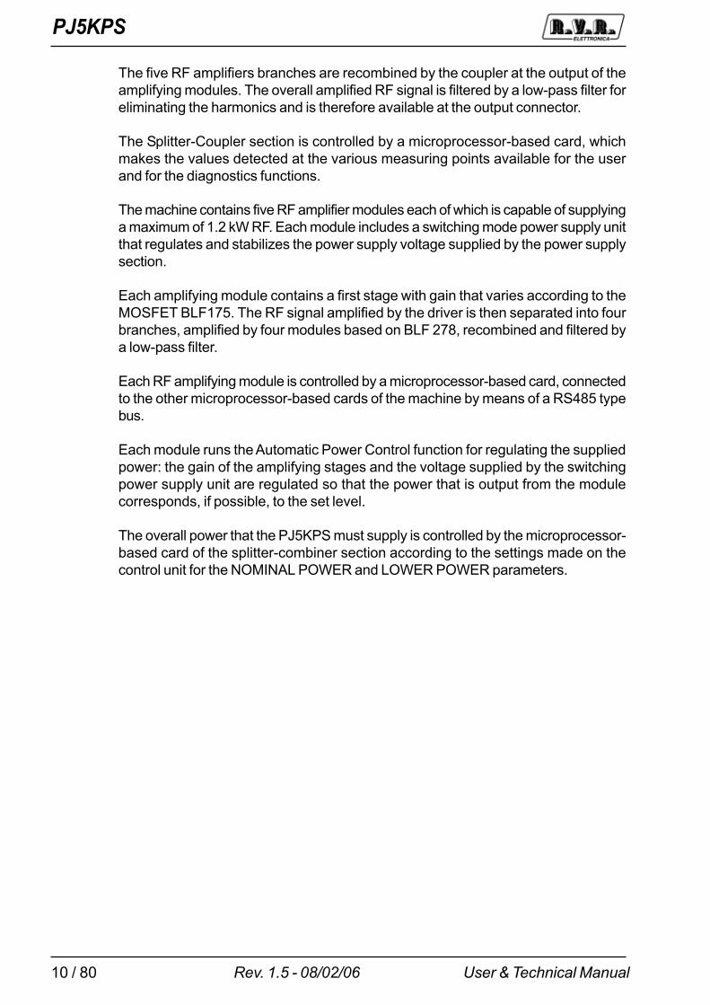
This description is based on the block diagram shown in Figure 4-1.
The PJ5KPS amplifier essentially comprises three blocks:
� The power supply section
� The Splitter-Coupler section
� The RF amplifier section
The power supply section of the PJ5KPS amplifier is made up of one or two three-phase transformers, each one associated with a rectifier circuit for generating thenon-stabilized voltage of 80V that supplies the RF modules. The transformers andthe rectifier circuits are mounted on removable carriages together with powerinductors that help achieve a power factor of about 94%.
The power supply unit carriage is dimensioned for supplying all the power requiredfor the PJ5KPS to operate at full power. Therefore the configuration of the machinewith two power supply unit carriages is a hot stand-by redundant one.
The power supply section is controlled by a microprocessor-based card installed inthe rack.
The Splitter-Coupler section performs all the treatment of the RF signal except for thepower amplification.

PJ5KPS
9 / 80User & Technical Manual Rev. 1.5 - 08/02/06
The RF signals generated by two exciters (in the redundant configuration) are firstattenuated by 6 dB to improve the uncoupling among the stages and then connectedto a coaxial relay commanded by the control unit. One of the two signals is closed ona dummy load built into the machine whereas the other signal is connected to theinput splitter. The power of both signals is measured by specific directional couplers.
The RF signal of the selected exciter is divided into five branches, each of which ispassed to the input of an amplifying module.
-6 d
B
-6 d
B
Exc
. 1R
F in
Exc
. 2R
F in
Tan
sfor
mer
/Rec
tifie
r
AC
in38
0 V
3F+
N
80 V
dc
Spl
itter
Cou
pler
-
Pow
ersu
pply
μC
Con
trol
Uni
t
1.2
kW R
F M
odul
e (5
x)
RF
Out
μC
Tan
sfor
mer
/Rec
tifie
r
RS
485
RS
485
μCR
S48
5
RS
485
Pow
erse
tting
Figure 4-1 Block diagram of the PJ5KPS
PJ5KPS
10 / 80 User & Technical ManualRev. 1.5 - 08/02/06
The five RF amplifiers branches are recombined by the coupler at the output of theamplifying modules. The overall amplified RF signal is filtered by a low-pass filter foreliminating the harmonics and is therefore available at the output connector.
The Splitter-Coupler section is controlled by a microprocessor-based card, whichmakes the values detected at the various measuring points available for the userand for the diagnostics functions.
The machine contains five RF amplifier modules each of which is capable of supplyinga maximum of 1.2 kW RF. Each module includes a switching mode power supply unitthat regulates and stabilizes the power supply voltage supplied by the power supplysection.
Each amplifying module contains a first stage with gain that varies according to theMOSFET BLF175. The RF signal amplified by the driver is then separated into fourbranches, amplified by four modules based on BLF 278, recombined and filtered bya low-pass filter.
Each RF amplifying module is controlled by a microprocessor-based card, connectedto the other microprocessor-based cards of the machine by means of a RS485 typebus.
Each module runs the Automatic Power Control function for regulating the suppliedpower: the gain of the amplifying stages and the voltage supplied by the switchingpower supply unit are regulated so that the power that is output from the modulecorresponds, if possible, to the set level.
The overall power that the PJ5KPS must supply is controlled by the microprocessor-based card of the splitter-combiner section according to the settings made on thecontrol unit for the NOMINAL POWER and LOWER POWER parameters.
PJ5KPS
11 / 80User & Technical Manual Rev. 1.5 - 08/02/06
5. Installation and useThis chapter contains the basic instructions for installing and using the PJ5KPSamplifier. If necessary, more in-depth information about the operating principles maybe traced in the next chapters.
5.1 Assembly
For practical reasons and for transport safety, the machine is usually supplied disas-sembled to the customer. The assembly procedure is rather simple and can be car-ried out by any qualified technician.
Caution: In order to avoid the risk of damaging the machine and/or of injuring theoperators, it is advisable to closely adhere to the instructions provided below. alwaysrespect all the safety regulations and standards in force.
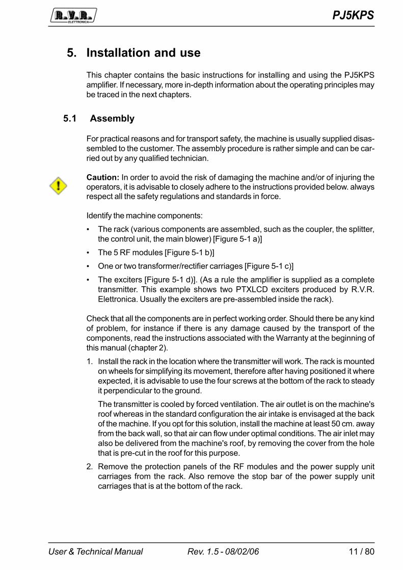
Identify the machine components:
� The rack (various components are assembled, such as the coupler, the splitter,the control unit, the main blower) [Figure 5-1 a)]
� The 5 RF modules [Figure 5-1 b)]
� One or two transformer/rectifier carriages [Figure 5-1 c)]
� The exciters [Figure 5-1 d)]. (As a rule the amplifier is supplied as a completetransmitter. This example shows two PTXLCD exciters produced by R.V.R.Elettronica. Usually the exciters are pre-assembled inside the rack).
Check that all the components are in perfect working order. Should there be any kindof problem, for instance if there is any damage caused by the transport of thecomponents, read the instructions associated with the Warranty at the beginning ofthis manual (chapter 2).
1. Install the rack in the location where the transmitter will work. The rack is mountedon wheels for simplifying its movement, therefore after having positioned it whereexpected, it is advisable to use the four screws at the bottom of the rack to steadyit perpendicular to the ground.
The transmitter is cooled by forced ventilation. The air outlet is on the machine'sroof whereas in the standard configuration the air intake is envisaged at the backof the machine. If you opt for this solution, install the machine at least 50 cm. awayfrom the back wall, so that air can flow under optimal conditions. The air inlet mayalso be delivered from the machine's roof, by removing the cover from the holethat is pre-cut in the roof for this purpose.
2. Remove the protection panels of the RF modules and the power supply unitcarriages from the rack. Also remove the stop bar of the power supply unitcarriages that is at the bottom of the rack.
PJ5KPS
12 / 80 User & Technical ManualRev. 1.5 - 08/02/06
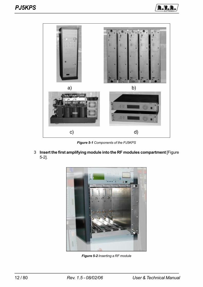
3 Insert the first amplifying module into the RF modules compartment [Figure5-2].
a) b)
c) d)
Figure 5-1 Components of the PJ5KPS
Figure 5-2 Inserting a RF module

PJ5KPS
13 / 80User & Technical Manual Rev. 1.5 - 08/02/06
The modules have a groove at the top and one at the bottom: insert the modulesso that the guides in the compartment fit into these grooves. Slide the moduleuntil the two fixing screws fit into their seats. Then tighten the fixing screws at thesame time so that the module inserts into its compartment remaining parallel untilit is perfectly in place.
4. Repeat the operation with the other four RF modules.
5. Insert the first transformer carriage into the left-hand side of the specificcompartment. The carriage is mounted on three wheels (two are fixed on the frontside and one pivoting rear wheel) to facilitate this operation. Move the carriagetoward the left-hand wall of the rack [Figure 5-3] and then move it forward until theconnectors at the back are perfectly in-serted into their seats.
!The power supply unit carriage is very heavy and its barycenter is high, therefore becareful when handling it to avoid tipping it over.6. If you have a redundant power supply unit, insert the second power supply unit
carriage as you did with the first one.
7. Position the stop bar of the power supply unit carriages.
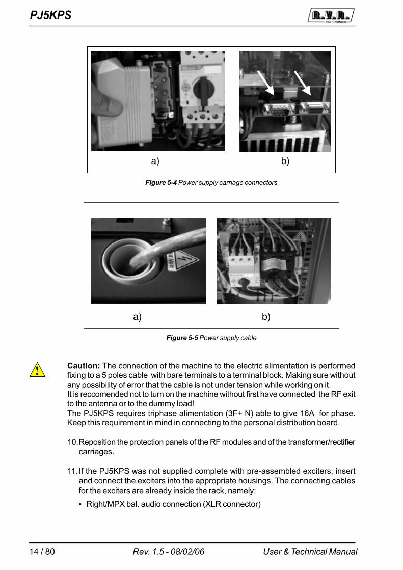
8. Make the necessary connections of the power supply unit carriages :
� Power supply connector [Figure 5-4 a)]
� Data connectors [Figure 5-4 b)]
9. Connect the machine's main power supply cable. Route the cable (5-pole type)through the raceway on the machine's roof [Figure 5-5 a)] and fix the conductorsto the terminals of the master switch [Figure 5-5 b)]. The last operation is usuallyperformed by removing the knob and the cover of the isolating switch.
Figure 5-3 Power supply carriage connectors
PJ5KPS
14 / 80 User & Technical ManualRev. 1.5 - 08/02/06
! Caution: The connection of the machine to the electric alimentation is performedfixing to a 5 poles cable with bare terminals to a terminal block. Making sure withoutany possibility of error that the cable is not under tension while working on it.It is reccomended not to turn on the machine without first have connected the RF exitto the antenna or to the dummy load!The PJ5KPS requires triphase alimentation (3F+ N) able to give 16A for phase.Keep this requirement in mind in connecting to the personal distribution board.
10.Reposition the protection panels of the RF modules and of the transformer/rectifiercarriages.
11. If the PJ5KPS was not supplied complete with pre-assembled exciters, insertand connect the exciters into the appropriate housings. The connecting cablesfor the exciters are already inside the rack, namely:
� Right/MPX bal. audio connection (XLR connector)
a) b)
Figure 5-4 Power supply carriage connectors
a) b)
Figure 5-5 Power supply cable

PJ5KPS
15 / 80User & Technical Manual Rev. 1.5 - 08/02/06
� Left/Mono audio connection (XLR connector)
� MPX unbal. audio connection (BNC connector)
� Power supply (VDE connector)
� Control connector (DB15 connector)
Now you may may perform the preliminary checks on the amplifier and start it up.
NB The connectors on the roof of the machine are not in parallel but directly connect tothe eciters (L and R exciter 1, L and R exciter 2 etc). Keep this in mind to make theaudio connections, that in some cases can require,for example, the use of an audiodistributor.
5.2 Amplifier check
The operator controls and checks the status of the PJ5KPS by means of the controlunit. Three control groups are present on this unit:
o LCD and scroll buttons
o Buttons, selector switches and LEDs
o Analog instrument and rotary selector switch
PJ5KPS
16 / 80 User & Technical ManualRev. 1.5 - 08/02/06
5.2.1 Display LCD
The operator uses the control software of the transmitter by means of a series ofmenus that are displayed on the LCD. Four specific keys are provided for scrollingthrough the menus, performing the settings and giving the commands:
Pulsante DescrizioneOK Click this button to access a sub-menu, to enter the editing mode or to
confirm a modified value.ESC Click this button to exit from a menu or to cancel the modification of a
value.Click this button to scroll inside a menu (to the right or down) or toreduce the value of a parameter being modified.Click this button to scroll inside a menu (to the left or up) or to increasethe value of a parameter being modified.
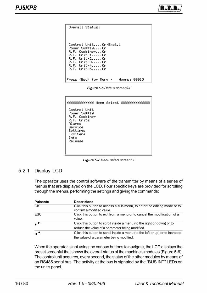
When the operator is not using the various buttons to navigate, the LCD displays thepreset screenful that shows the overall status of the machine's modules (Figure 5-6).The control unit acquires, every second, the status of the other modules by means ofan RS485 serial bus. The activity at the bus is signaled by the "BUS INT" LEDs onthe unit's panel.
Figure 5-6 Default screenful
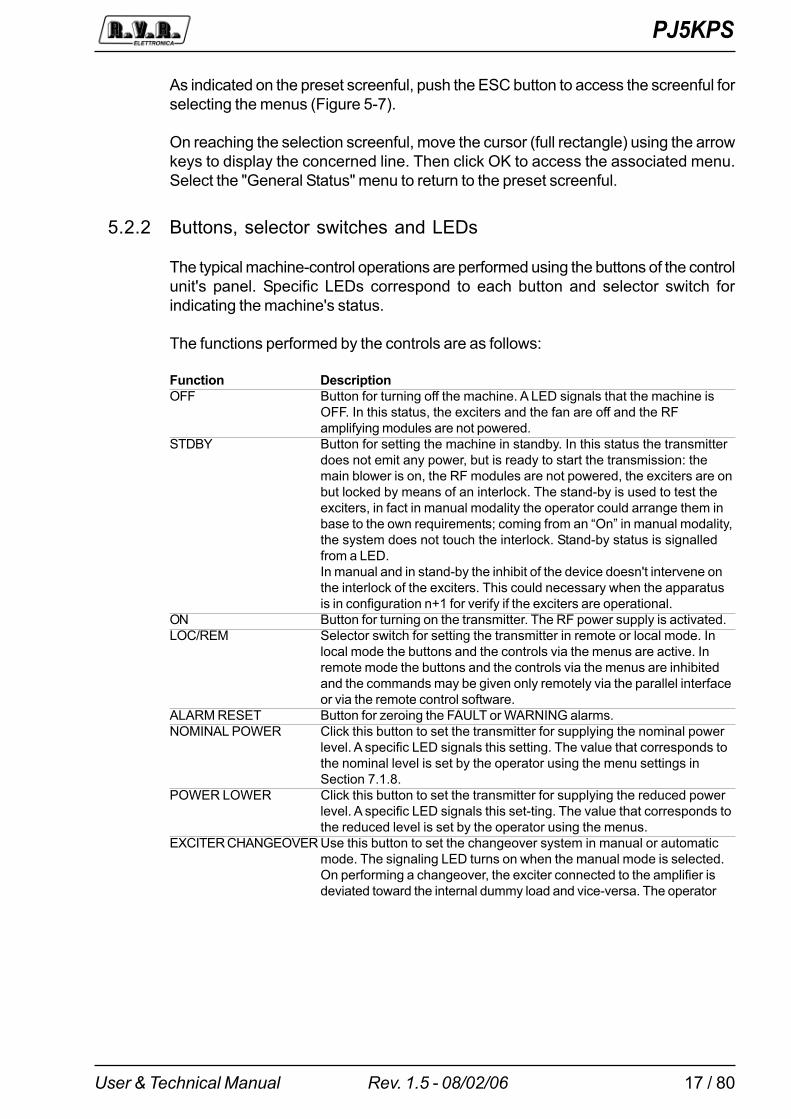
Figure 5-7 Menu select screenful
PJ5KPS
17 / 80User & Technical Manual Rev. 1.5 - 08/02/06
As indicated on the preset screenful, push the ESC button to access the screenful forselecting the menus (Figure 5-7).
On reaching the selection screenful, move the cursor (full rectangle) using the arrowkeys to display the concerned line. Then click OK to access the associated menu.Select the "General Status" menu to return to the preset screenful.
5.2.2 Buttons, selector switches and LEDs
The typical machine-control operations are performed using the buttons of the controlunit's panel. Specific LEDs correspond to each button and selector switch forindicating the machine's status.
The functions performed by the controls are as follows:
Function DescriptionOFF Button for turning off the machine. A LED signals that the machine is
OFF. In this status, the exciters and the fan are off and the RFamplifying modules are not powered.
STDBY Button for setting the machine in standby. In this status the transmitterdoes not emit any power, but is ready to start the transmission: themain blower is on, the RF modules are not powered, the exciters are onbut locked by means of an interlock. The stand-by is used to test theexciters, in fact in manual modality the operator could arrange them inbase to the own requirements; coming from an �On� in manual modality,the system does not touch the interlock. Stand-by status is signalledfrom a LED.In manual and in stand-by the inhibit of the device doesn't intervene onthe interlock of the exciters. This could necessary when the apparatusis in configuration n+1 for verify if the exciters are operational.
ON Button for turning on the transmitter. The RF power supply is activated.LOC/REM Selector switch for setting the transmitter in remote or local mode. In
local mode the buttons and the controls via the menus are active. Inremote mode the buttons and the controls via the menus are inhibitedand the commands may be given only remotely via the parallel interfaceor via the remote control software.
ALARM RESET Button for zeroing the FAULT or WARNING alarms.NOMINAL POWER Click this button to set the transmitter for supplying the nominal power
level. A specific LED signals this setting. The value that corresponds tothe nominal level is set by the operator using the menu settings inSection 7.1.8.
POWER LOWER Click this button to set the transmitter for supplying the reduced powerlevel. A specific LED signals this set-ting. The value that corresponds tothe reduced level is set by the operator using the menus.
EXCITER CHANGEOVER Use this button to set the changeover system in manual or automaticmode. The signaling LED turns on when the manual mode is selected.On performing a changeover, the exciter connected to the amplifier isdeviated toward the internal dummy load and vice-versa. The operator

PJ5KPS
18 / 80 User & Technical ManualRev. 1.5 - 08/02/06
must use the exciters menu to perform the changeover in manual mode.LEDs (Wait, Warning, Fault) Other signaling LEDs are connected to the alarm states and to
the serial data transmissions that take place among themicroprocessorbased cards. The function of these LEDs is describedfurther on in this manual.
5.2.3 Analog instruments
The control unit of PJ5KPS contains an analog meter with a rotating selector that areuseful for an immediate display of the following parameters:
FWD PWR Transmitter direct powerRFL PWR Transmitter reflected powerUNBAL Transmitter unbalancing powerPWR EXC1 Power supplied by the exciter currently connected to the amplifier. This
value is measured by the machine in the splitter sectionPWR EXC2 Power supplied by the exciter currently connected to the internal load.
This value is measured by the amplifier in the splitter sectionEXT FWD PWR Direct power of an external combiner.EXT RFL FWD Reflected power of an external combiner.EXT UNBAL Unbalancing power of an external combiner.
These three values are used when the transmitter is connected to a 1+1system. The SET outputs may also be connected to these quantities.
5.3 First start
This section describes the procedure for powering-on the machine the first time.
For simplicity's sake, the automatic control capacities of the exciters are temporarilydisabled.
Refer to chapter 5.4 that provides the instructions for turning on the PJ5KPS in thevarious cases.
5.3.1 Preliminary operation
Before activating this piece of equipment, the necessary connections must beperformed, and in particular:
� Power supply
� Modulating signals (Audio or MPX, RDS...)
� RF load (antenna feeder or dummy load)
About to the connections of the power supply and the modulating signals, pleaserefer to chapter 5.1.
PJ5KPS
19 / 80User & Technical Manual Rev. 1.5 - 08/02/06
The machine's RF output is the "EIA 1 5/8" flanged type and is accessed on the roofof the PJ5KPS. If a dummy load capable of dissipating the RF power generated bythe transmitter is available, it is advisable to run the first tests by connecting to itrather than to the transmission antenna.
5.3.2 Power-on
When powering-on the transmitter the first time, perform the operations outlined inthe table below.
The "Result" column indicates the immediate results of the operations performedplus a few indications that confirm that the machine is working efficiently.
Should any inconsistencies occur as compared to these indications, interrupt theprocedure and identify the reason for the malfunction before resuming the procedure.
Operation ResultClose the "Transformer Breaker" isolating switches
The power supply unit carriages are poweredTurn the "Mains" switch The whole transmitter is powered. The machine is activated in the same
status it was in when it was turned off the last timePress the OFF key of the control unit
RF emission by the transmitter is inhibited; the exciters are off; the RFamplifier modules are off
Press the EXCITER CHANGEOVER key of the control unitThe automatic management for the exciters changeover is disabled. TheMANUAL LED must be on (otherwise press the key again)
Press the STDBY key of the control unitThe exciters are turned on in interlock status. The RF amplifyingmodules stay disabled. Being in manual modality, the exciters could beunlocked to verify the operation (see 5.3.3).
Set the parameters of the control unitThis procedure is described in chapter 5.3.3 on in this manual. Thecontrol unit communicates the nominal power and reduced power valuesto the RF modules. It also handles the coaxial relays so that the on airexciter is the desired one and sets the exciter to ON mode
Set the exciters Adhere to the instructions of the exciters used for setting the requiredwork frequency on the exciters. Regulate the output power of theexciters to 20 W.
Press POWER LOWER and ONThe current exciter is activated (the interlock is released from theexciter) and its power emission is enabled. The power emitted by thePJ5KPS amplifier increases gradually until it attains the level that hadbeen set previously as "Reduced power". Check the emitted power levelby means of the analog instrument with the selector switched to FWDPWR position
Press NOMINAL POWERPower supplied by PJ5KPS increases and attains the set nominalvalue. Check it on the analog instrument.
When the transmitter is on and works at its nominal power, the whole series of"accessory" checks and settings deemed necessary may be carried out beforestarting up the apparatus.

PJ5KPS
20 / 80 User & Technical ManualRev. 1.5 - 08/02/06
5.3.3 Control unit settings
The settings of the control unit that are required for starting up the machine, mentionedin the powering-on procedure, are the following:
1. Setting of the power levels
2. Setting of the on air exciter
Before performing the first operation, click the ESC button. The display shows thescreenful for selecting the menus [Figure 5-7]. Click the arrow keys until the cursorhighlights the line associated with the Setting menu. Click OK: the software will showthe associated screenful on the display [Figure 5-8].
On having accessed the Settings menu, use the arrow keys to select the nominalpower line (Pwr. Out) and click OK. Use the arrow keys to decrease or increase theindicated percentage value up to the required level. Click OK again to set this value.Repeat the operation for the line associated with the reduced power level (Pwr. Lower).
NBThe new power level is transmitted to the combiner module and then stored inEEPROM only when the ESC button is clicked.
When inside this menu, it is advisable to check the date and time lines and updatethem if necessary. Note: the date and time are used only for marking the events in thealarms register.
NB The date and time do not need to be updated in the transmitter in order for it to workefficiently.
On having completed these settings, click ESC to return to the selection screenful.
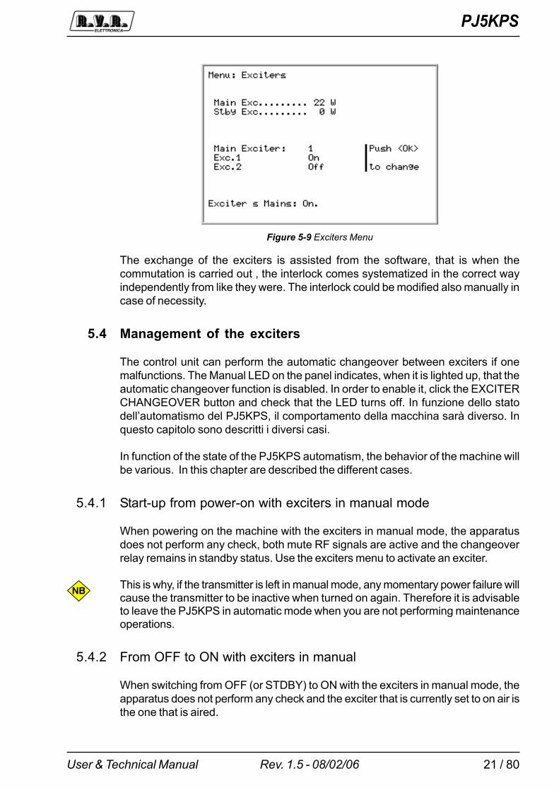
In order to set the on air exciter, select the Exciters menu [Figure 5-9]. Take intoconsideration the On Air Exciter line: the number to the right indicates the exciterbeing used. To change it simply highlight the line and click OK.
Figure 5-8 Menù settings
PJ5KPS
21 / 80User & Technical Manual Rev. 1.5 - 08/02/06
The exchange of the exciters is assisted from the software, that is when thecommutation is carried out , the interlock comes systematized in the correct wayindependently from like they were. The interlock could be modified also manually incase of necessity.
5.4 Management of the exciters
The control unit can perform the automatic changeover between exciters if onemalfunctions. The Manual LED on the panel indicates, when it is lighted up, that theautomatic changeover function is disabled. In order to enable it, click the EXCITERCHANGEOVER button and check that the LED turns off. In funzione dello statodell�automatismo del PJ5KPS, il comportamento della macchina sarà diverso. Inquesto capitolo sono descritti i diversi casi.
In function of the state of the PJ5KPS automatism, the behavior of the machine willbe various. In this chapter are described the different cases.
5.4.1 Start-up from power-on with exciters in manual mode
When powering on the machine with the exciters in manual mode, the apparatusdoes not perform any check, both mute RF signals are active and the changeoverrelay remains in standby status. Use the exciters menu to activate an exciter.
NB This is why, if the transmitter is left in manual mode, any momentary power failure willcause the transmitter to be inactive when turned on again. Therefore it is advisableto leave the PJ5KPS in automatic mode when you are not performing maintenanceoperations.
5.4.2 From OFF to ON with exciters in manual
When switching from OFF (or STDBY) to ON with the exciters in manual mode, theapparatus does not perform any check and the exciter that is currently set to on air isthe one that is aired.
Figure 5-9 Exciters Menu

PJ5KPS
22 / 80 User & Technical ManualRev. 1.5 - 08/02/06
If the mains signal is not OK, the exciters turn off automatically.
If the maximum drive power is exceeded during operations (> 35W), the PJ5KPS isset to fault status and power supply is cut to the exciters.A message in the alarmsmenu signals this fault.
When the apparatus is set to STDBY, the mute RF signals of the exciters are notactivated and may be modified by the operator.
When the apparatus is set to EXT INT or AUX INT, the mute RF signals of the excitersare not activated and may be modified by the operator.
5.4.3 Automatic changeover
When the PJ5KPS is in the exciter automatic changeover mode, the power emittedby the on air exciter is checked constantly. If at any time the on air exciter is no longergood (i.e. power drops to below the preset level), the apparatus is kept operationalwhereas the exciter connected to the internal Dummy Load turns on. If the latter oneis good (i.e. it is capable of supplying the required power), then the two exciters arechanged over. Instead if the alternative exciter is not good, no changeover takesplace, the control unit commands the mute RF of the exciter to Dummy Load, it waits120 s. and repeats the attempt. This procedure is repeated indefinitely until one ofthe two exciters is considered to be good.
During the whole length of time during which there is no good exciter, the PJ5KPSkeeps the WAIT LED on for signaling this status.
Each exciter is fitted with its own mute RF. On being commanded, the piloting signalmust return to zero within 3 seconds at the most. If this does not occur, the fault isrecorded by an error message that is entered in the alarms menu.
If the mains signal is not OK, the exciters turn off automatically. If the piloting powerexceeds the limit during operations, the PJ5KPS is set to the FAULT status and thepower supply of the exciters is turned off. A message in the alarms menu signals thefault. Keep in mind that the operator's intervention is required to exit from the FAULTstatus.
If the MAINS signal coming from the bus is not OK, the exciters are all turned off. Assoon as the MAINS signal is regular again, the evaluation cycle of the exciters begins(see 5.4.4).
When the apparatus is set to STDBY, the mute RF signals of the exciters are activatedand as such both exciters are inhibited. If the ON key is pressed, the system re-evaluates both exciters in the same manner as in the procedure from OFF to ON(see 5.4.4).
PJ5KPS
23 / 80User & Technical Manual Rev. 1.5 - 08/02/06
When the apparatus is set to EXT INT or AUX INT, the mute RF signals of the excitersare activated and therefore both exciters are inhibited. When the external interlocksare released, the system re-evaluates both exciters as during the phase from OFF toON (see 5.4.4).
5.4.4 Phase from ON to OFF
When the apparatus is set to OFF status and you press the ON button, the powersupply of the exciters is activated and the logic starts to evaluate the exciters. Duringthe evaluation phase, the WAIT LED stays ON.
When the apparatus is turned OFF, it memorizes the exciter on air. Consequentlywhen the machine restarts it can attempt to restore the previous conditions. On themachine restarting, if the exciter that is to be aired does not attain the preset powerlevel whereas the spare one is operational, the apparatus performs the changeoverwhen the evaluation time (120 s.) expires.
On the machine restarting, if both exciters do not attain the preset power level, theapparatus airs the one that had been present when the machine was turned off, afterthe evaluation time has expired.
5.4.5 Start-up with exciters in automatic mode
The sequence run by the PJ5KPS, when the power supply is activated while it isalready in ON status and the exciters are in automatic mode, is identical to the onerun for switching from OFF to ON. The only difference is that a screenful displays thecountdown for determining the fault of the exciters. During this phase the manual/automatic button is inhibited and in order to set the exciters to manual mode youmust press the OFF button of the apparatus.
5.4.6 Audio alarm
The control unit of the PJ5KPS can manage a fault signal, for each exciter, whichnormally has an "Audio Alarm" meaning. The control software of the PJ5KPS doesnot intervene in triggering these signals since they must be checked by the exciters(or by any other connected devices).
The Audio Alarm signals are made up of two inputs for the logical signals on theparallel interface and on the "mute RF" command connector of the exciters.
The control unit manages these signals just like it manages the power good signals:
� Each "Audio alarm" signal is associated with its own exciter
� If the audio signal, associated with the exciter that is currently on air, enters analarm status, the PJ5KPS waits for the time configured in the exciter menu beforeit attempts the restoring operation
PJ5KPS
24 / 80 User & Technical ManualRev. 1.5 - 08/02/06
� If the audio of the aired exciter is still in alarm status on the elapsing of the aforesaidtime interval, the control unit checks if the audio of the exciter on the dummy loadis regular. In this case the changeover between the exciters is performed.
Observe the following differences as compared to the case in which power is missing:
� The management of the "Audio alarm" signals is not active during the start-upphase and during the switching phase from OFF to ON, but only when the excitersare working in automatic.
� In the standard configuration, the aforesaid sequence continues until the audiosignal associated with one of the exciters becomes regular again. In the "N+1"configuration, the switching attempt is performed only twice, after which thePJ5KPS enters the fault status.
� An Audio Alarm output is provided on the parallel interface: this signal is activated(with no delays) when the audio of the exciter that is currently on air is in alarmstatus.
5.5 Protection and alarms
The PJ5KPS contains a complete protection and alarms system, both at the individ-ual modules level and at the control unit level.
The modules are fitted with a micro-processor-based system that manages anymalfunctions locally. The associated information is communicated to the control unitfor displaying and storing the events and for the centralized management of the eventsthat require it.
Certain LEDs of the PJ5KPS panel are dedicated to the management of the alarms:
LED DescriptionWARNING This LED indicates a warning (something is not correctly working, but
the amplifier is still working)FAULT This LED indicates a fault (the amplifier is shut off, the operator�s
intervention is required)WAIT This LED indicates the wait status (the amplifier is temporarily off, it will
be restarted as soon as the reason that keeps it from working will beremoved, or after a fixed amount of time depending on the reason of theintervention of the protection system)
The ALARM RESET button is used for resetting the alarms and restarting the machine.
A complete description of the alarms and protection system is given in chapter 7.5.
PJ5KPS
25 / 80User & Technical Manual Rev. 1.5 - 08/02/06
6. Troubleshooting[This chapter will be filled in the next edition of the present manual]
PJ5KPS
26 / 80 User & Technical ManualRev. 1.5 - 08/02/06
7. Technical description
7.1 Software - Reference guide
This chapter gives a point to point description of the screens composing the softwareof the PJ5KPS.
NB Since the management software is able to control up to 10 modules, some of themenus configurate themselves for the number of modules. For example, in a PJ10KPSthe menu Overall Status has ten �RF Unit� lines as in the general example reported inthe manual, in the PJ5KPS only five of them will be shown.
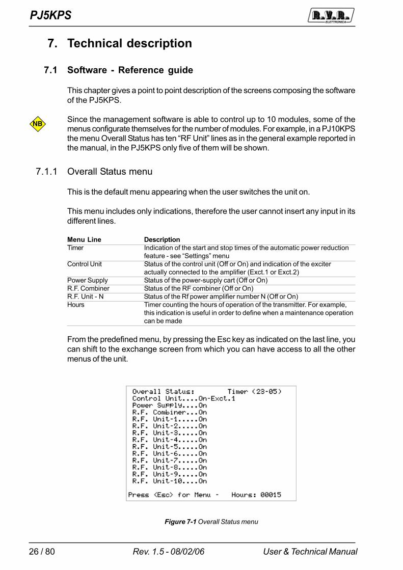
7.1.1 Overall Status menu
This is the default menu appearing when the user switches the unit on.
This menu includes only indications, therefore the user cannot insert any input in itsdifferent lines.
Menu Line DescriptionTimer Indication of the start and stop times of the automatic power reduction
feature - see �Settings� menuControl Unit Status of the control unit (Off or On) and indication of the exciter
actually connected to the amplifier (Exct.1 or Exct.2)Power Supply Status of the power-supply cart (Off or On)R.F. Combiner Status of the RF combiner (Off or On)R.F. Unit - N Status of the Rf power amplifier number N (Off or On)Hours Timer counting the hours of operation of the transmitter. For example,
this indication is useful in order to define when a maintenance operationcan be made
From the predefined menu, by pressing the Esc key as indicated on the last line, youcan shift to the exchange screen from which you can have access to all the othermenus of the unit.
Figure 7-1 Overall Status menu

PJ5KPS
27 / 80User & Technical Manual Rev. 1.5 - 08/02/06
7.1.2 Select menu
This is the exchange menu from which you can select the different sub-menus thatcompose the software.
In order to enter a sub-menu, select the correspondent line with the arrow buttonsand press Enter.
Menu Line DescriptionGeneral Status General status of the PJ5KPSPower Supply Status of the power-supply cartR.F. Combiner Status of the RF combinerR.F. Units Status of the RF power amplifiersAlarms Summary of the occured alarmsService Service menu for the switching on/off of the modulesSettings Setting of the parameters (i.e. Power levels)Exciters Parameters of the exciters (i.e. output power, on air exciter)Info Information concerning the configuration of the PJ5KPSRelease Information concerning the hardware and software versions of the
modules composing the unitModem Settings related to the optional telemetry system (see chap.9)
To return to the predefined menu, select General Status and press OK.
Figure 7-2 Select menu
PJ5KPS
28 / 80 User & Technical ManualRev. 1.5 - 08/02/06
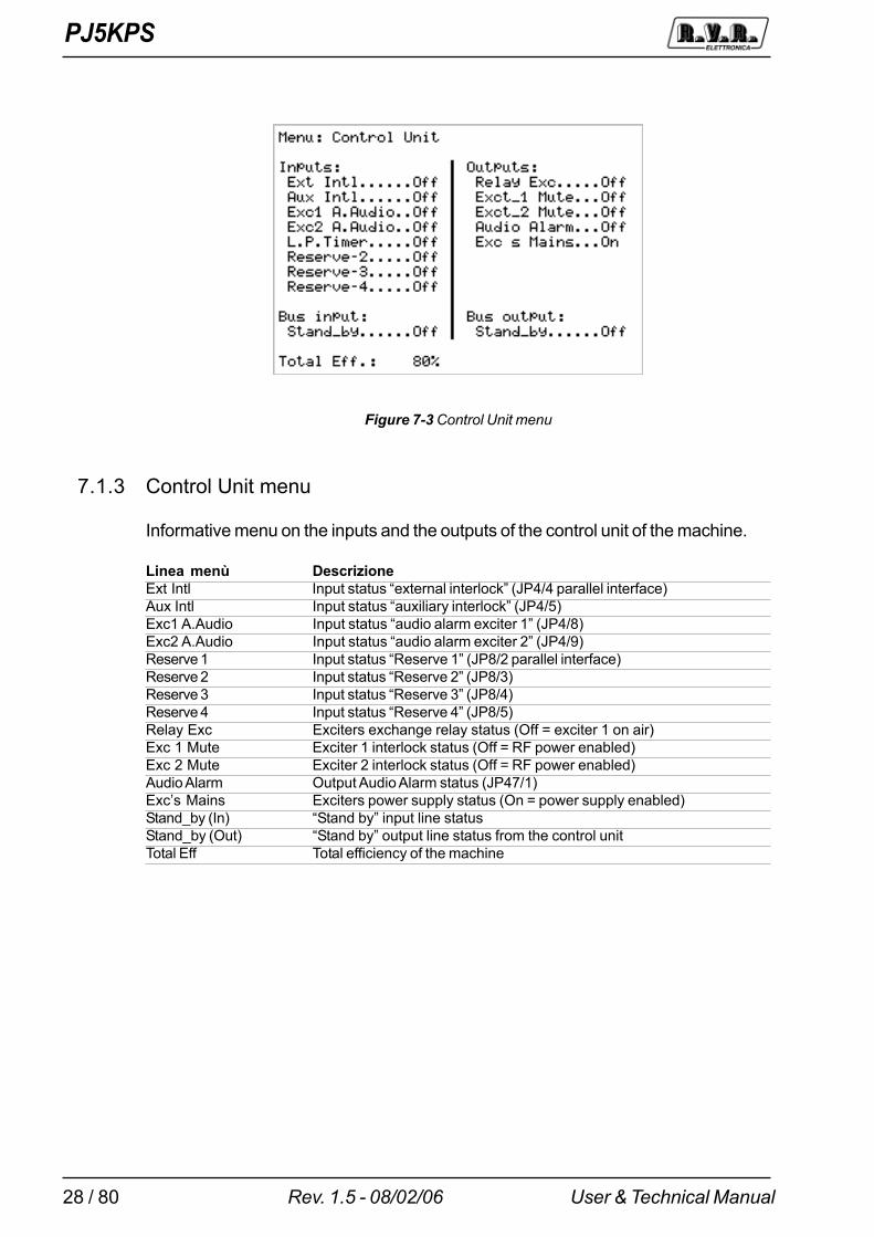
7.1.3 Control Unit menu
Informative menu on the inputs and the outputs of the control unit of the machine.
Linea menù DescrizioneExt Intl Input status �external interlock� (JP4/4 parallel interface)Aux Intl Input status �auxiliary interlock� (JP4/5)Exc1 A.Audio Input status �audio alarm exciter 1� (JP4/8)Exc2 A.Audio Input status �audio alarm exciter 2� (JP4/9)Reserve 1 Input status �Reserve 1� (JP8/2 parallel interface)Reserve 2 Input status �Reserve 2� (JP8/3)Reserve 3 Input status �Reserve 3� (JP8/4)Reserve 4 Input status �Reserve 4� (JP8/5)Relay Exc Exciters exchange relay status (Off = exciter 1 on air)Exc 1 Mute Exciter 1 interlock status (Off = RF power enabled)Exc 2 Mute Exciter 2 interlock status (Off = RF power enabled)Audio Alarm Output Audio Alarm status (JP47/1)Exc�s Mains Exciters power supply status (On = power supply enabled)Stand_by (In) �Stand by� input line statusStand_by (Out) �Stand by� output line status from the control unitTotal Eff Total efficiency of the machine
Figure 7-3 Control Unit menu
PJ5KPS
29 / 80User & Technical Manual Rev. 1.5 - 08/02/06
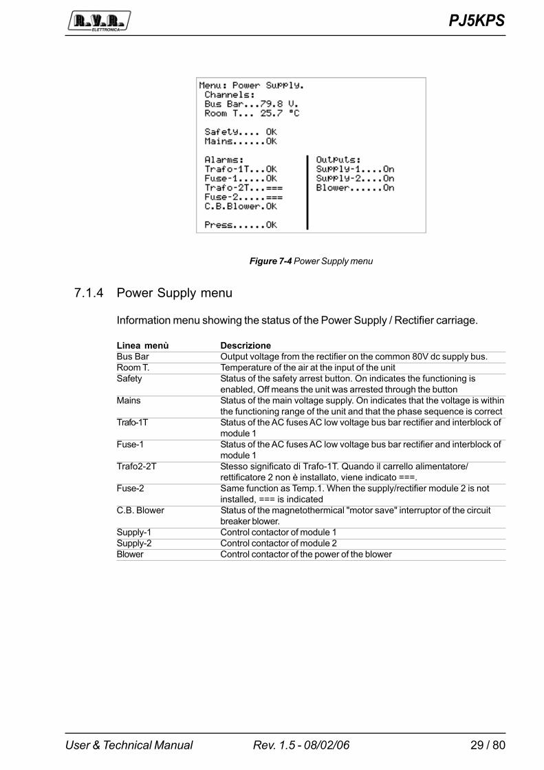
7.1.4 Power Supply menu
Information menu showing the status of the Power Supply / Rectifier carriage.
Linea menù DescrizioneBus Bar Output voltage from the rectifier on the common 80V dc supply bus.Room T. Temperature of the air at the input of the unitSafety Status of the safety arrest button. On indicates the functioning is
enabled, Off means the unit was arrested through the buttonMains Status of the main voltage supply. On indicates that the voltage is within
the functioning range of the unit and that the phase sequence is correctTrafo-1T Status of the AC fuses AC low voltage bus bar rectifier and interblock of
module 1Fuse-1 Status of the AC fuses AC low voltage bus bar rectifier and interblock of
module 1Trafo2-2T Stesso significato di Trafo-1T. Quando il carrello alimentatore/
rettificatore 2 non è installato, viene indicato ===.Fuse-2 Same function as Temp.1. When the supply/rectifier module 2 is not
installed, === is indicatedC.B. Blower Status of the magnetothermical "motor save" interruptor of the circuit
breaker blower.Supply-1 Control contactor of module 1Supply-2 Control contactor of module 2Blower Control contactor of the power of the blower
Figure 7-4 Power Supply menu
PJ5KPS
30 / 80 User & Technical ManualRev. 1.5 - 08/02/06
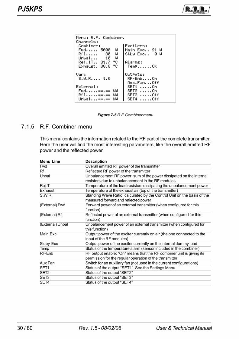
7.1.5 R.F. Combiner menu
This menu contains the information related to the RF part of the complete transmitter.Here the user will find the most interesting parameters, like the overall emitted RFpower and the reflected power.
Menu Line DescriptionFwd Overall emitted RF power of the transmitterRfl Reflected RF power of the transmitterUnbal Unbalancement RF power: sum of the power dissipated on the internal
resistors due to unbalanecement in the RF modulesRej.lT Temperature of the load resistors dissipating the unbalancement powerExhaust Temperature of the exhaust air (top of the transmitter)S.W.R. Standing Wave Ratio, calculated by the Control Unit on the basis of the
measured forward and reflected power(External) Fwd Forward power of an external transmitter (when configured for this
function)(External) Rfl Reflected power of an external transmitter (when configured for this
function)(External) Unbal Unbalancement power of an external transmitter (when configured for
this function)Main Exc Output power of the exciter currently on air (the one connected to the
input of the RF modules)Stdby Exc Output power of the exciter currently on the internal dummy loadTemp Status of the temperature alarm (sensor included in the combiner)RF-Enb RF output enable: �On� means that the RF combiner unit is giving its
permission for the regular operation of the transmitterAux Fan Switch for an auxiliary fan (not used in the current configurations)SET1 Status of the output �SET1�. See the Settings MenuSET2 Status of the output �SET2�SET3 Status of the output �SET3�SET4 Status of the output �SET4�
Figure 7-5 R.F. Combiner menu

PJ5KPS
31 / 80User & Technical Manual Rev. 1.5 - 08/02/06
7.1.6 R.F. Units menu
Information menu showing the status of the RF power amplifier modules. It is composedof 5 screens, one for each module, that can be scrolled using the arrow buttons.
Menu Line DescriptionFwd Measurement of the forward power of the amplifier moduleRfl Measurement of the forward power of the amplifier moduleInput Measurement of the driving power at the input of the amplifier moduleV.P.A. Measurement supply voltage of the module (generated from the
switching power supply included in each module)Driver Measurement of the current absorbed by the preamplifier stageMOS N Measurement of the current absorbed by the MOS N amplifier module
(each RF module contains 4 MOS modules)I. Tot Measurement of the total current absorbed by the RF moduleEff Efficiency of the amplifier module, as a result of the ratio between the
electrical power absorbed and the RF output powerTemp Temperature alarm, Ok or KoFuse Status of the fuse of the RF module: Ok or KoUnit. Intl State of the RF module interlock micro-switchRF enb. Enabled of power distribution from part of the module
Figure 7-6 R.F. Units menu
PJ5KPS
32 / 80 User & Technical ManualRev. 1.5 - 08/02/06
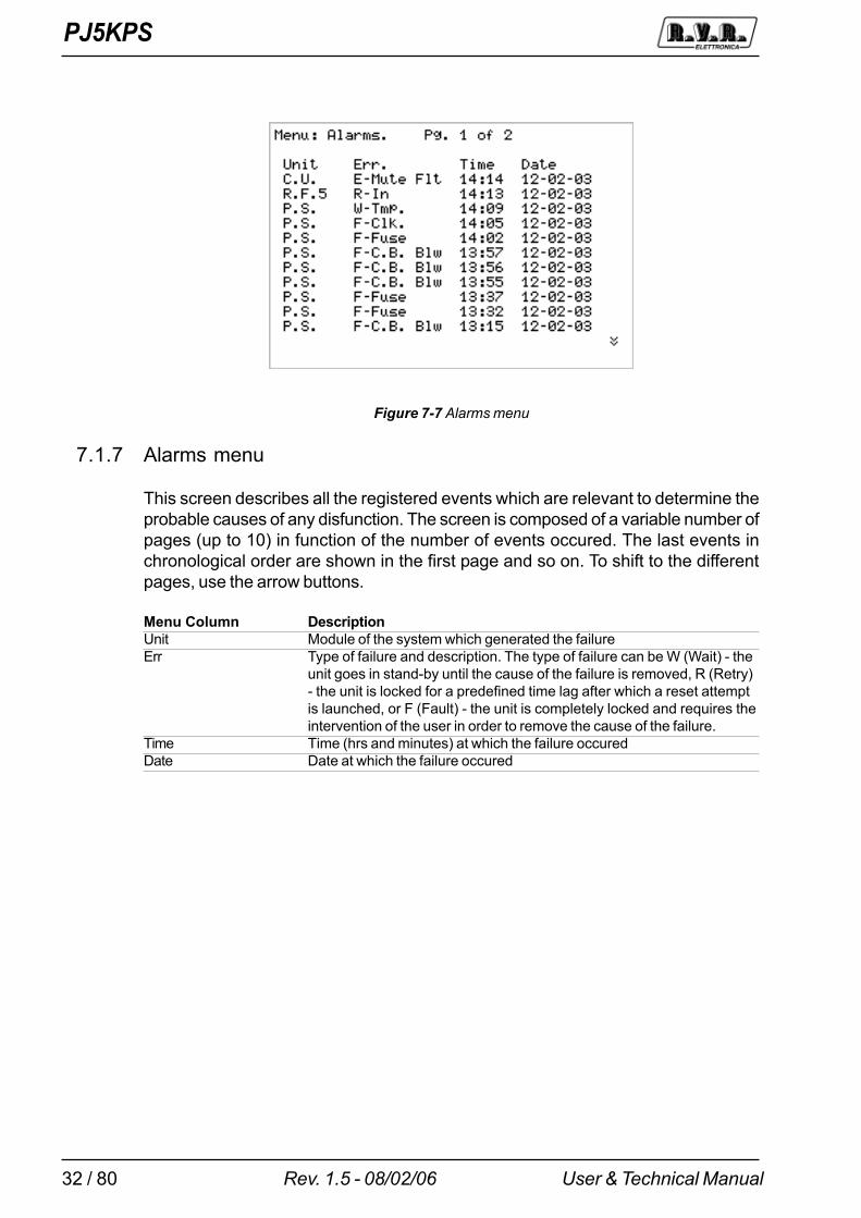
7.1.7 Alarms menu
This screen describes all the registered events which are relevant to determine theprobable causes of any disfunction. The screen is composed of a variable number ofpages (up to 10) in function of the number of events occured. The last events inchronological order are shown in the first page and so on. To shift to the differentpages, use the arrow buttons.
Menu Column DescriptionUnit Module of the system which generated the failureErr Type of failure and description. The type of failure can be W (Wait) - the
unit goes in stand-by until the cause of the failure is removed, R (Retry)- the unit is locked for a predefined time lag after which a reset attemptis launched, or F (Fault) - the unit is completely locked and requires theintervention of the user in order to remove the cause of the failure.
Time Time (hrs and minutes) at which the failure occuredDate Date at which the failure occured
Figure 7-7 Alarms menu
PJ5KPS
33 / 80User & Technical Manual Rev. 1.5 - 08/02/06
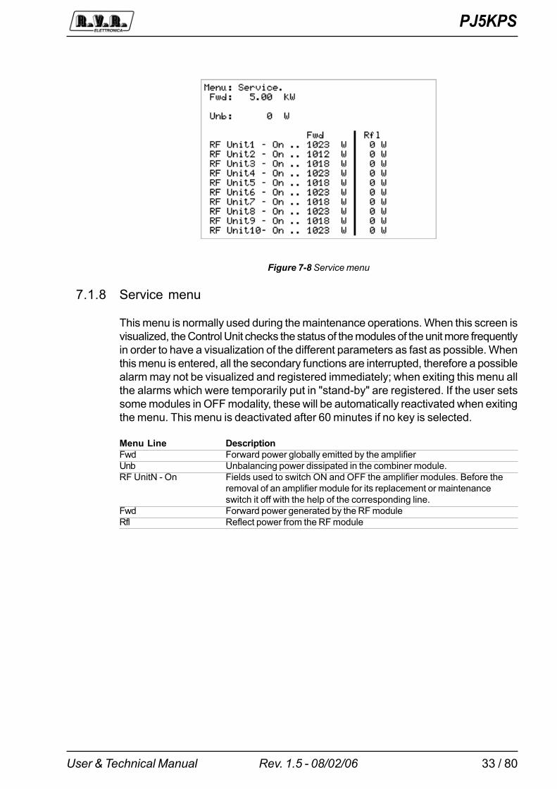
7.1.8 Service menu
This menu is normally used during the maintenance operations. When this screen isvisualized, the Control Unit checks the status of the modules of the unit more frequentlyin order to have a visualization of the different parameters as fast as possible. Whenthis menu is entered, all the secondary functions are interrupted, therefore a possiblealarm may not be visualized and registered immediately; when exiting this menu allthe alarms which were temporarily put in "stand-by" are registered. If the user setssome modules in OFF modality, these will be automatically reactivated when exitingthe menu. This menu is deactivated after 60 minutes if no key is selected.
Menu Line DescriptionFwd Forward power globally emitted by the amplifierUnb Unbalancing power dissipated in the combiner module.RF UnitN - On Fields used to switch ON and OFF the amplifier modules. Before the
removal of an amplifier module for its replacement or maintenanceswitch it off with the help of the corresponding line.
Fwd Forward power generated by the RF moduleRfl Reflect power from the RF module
Figure 7-8 Service menu
PJ5KPS
34 / 80 User & Technical ManualRev. 1.5 - 08/02/06
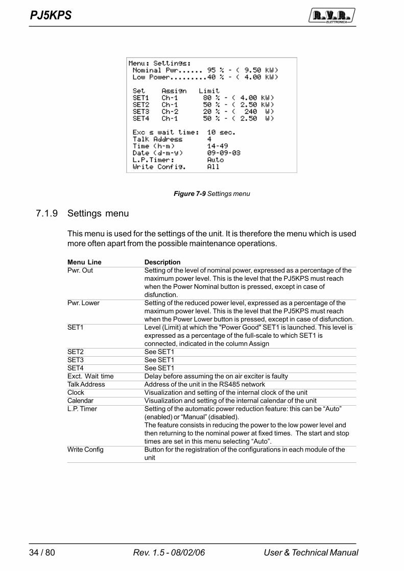
7.1.9 Settings menu
This menu is used for the settings of the unit. It is therefore the menu which is usedmore often apart from the possible maintenance operations.
Menu Line DescriptionPwr. Out Setting of the level of nominal power, expressed as a percentage of the
maximum power level. This is the level that the PJ5KPS must reachwhen the Power Nominal button is pressed, except in case ofdisfunction.
Pwr. Lower Setting of the reduced power level, expressed as a percentage of themaximum power level. This is the level that the PJ5KPS must reachwhen the Power Lower button is pressed, except in case of disfunction.
SET1 Level (Limit) at which the "Power Good" SET1 is launched. This level isexpressed as a percentage of the full-scale to which SET1 isconnected, indicated in the column Assign
SET2 See SET1SET3 See SET1SET4 See SET1Exct. Wait time Delay before assuming the on air exciter is faultyTalk Address Address of the unit in the RS485 networkClock Visualization and setting of the internal clock of the unitCalendar Visualization and setting of the internal calendar of the unitL.P. Timer Setting of the automatic power reduction feature: this can be �Auto�
(enabled) or �Manual� (disabled).The feature consists in reducing the power to the low power level andthen returning to the nominal power at fixed times. The start and stoptimes are set in this menu selecting �Auto�.
Write Config Button for the registration of the configurations in each module of theunit
Figure 7-9 Settings menu
PJ5KPS
35 / 80User & Technical Manual Rev. 1.5 - 08/02/06
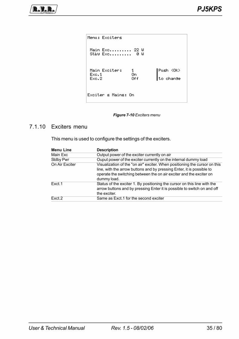
7.1.10 Exciters menu
This menu is used to configure the settings of the exciters.
Menu Line DescriptionMain Exc Output power of the exciter currently on airStdby Pwr Ouput power of the exciter currently on the internal dummy loadOn Air Exciter Visualization of the "on air" exciter. When positioning the cursor on this
line, with the arrow buttons and by pressing Enter, it is possible tooperate the switching between the on air exciter and the exciter ondummy load.
Exct.1 Status of the exciter 1. By positioning the cursor on this line with thearrow buttons and by pressing Enter it is possible to switch on and offthe exciter.
Exct.2 Same as Exct.1 for the second exciter
Figure 7-10 Exciters menu
PJ5KPS
36 / 80 User & Technical ManualRev. 1.5 - 08/02/06
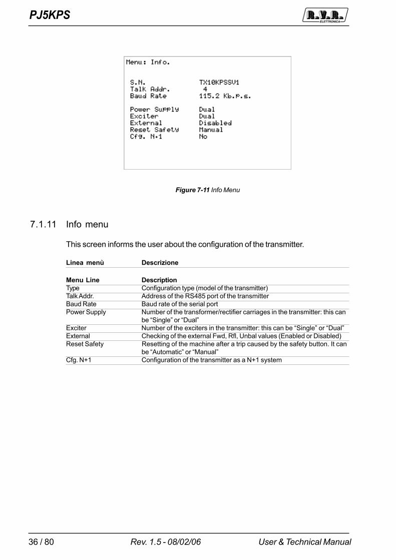
Figure 7-11 Info Menu
7.1.11 Info menu
This screen informs the user about the configuration of the transmitter.
Linea menù Descrizione
Menu Line DescriptionType Configuration type (model of the transmitter)Talk Addr. Address of the RS485 port of the transmitterBaud Rate Baud rate of the serial portPower Supply Number of the transformer/rectifier carriages in the transmitter: this can
be �Single� or �Dual�Exciter Number of the exciters in the transmitter: this can be �Single� or �Dual�External Checking of the external Fwd, Rfl, Unbal values (Enabled or Disabled)Reset Safety Resetting of the machine after a trip caused by the safety button. It can
be �Automatic� or �Manual�Cfg. N+1 Configuration of the transmitter as a N+1 system
PJ5KPS
37 / 80User & Technical Manual Rev. 1.5 - 08/02/06
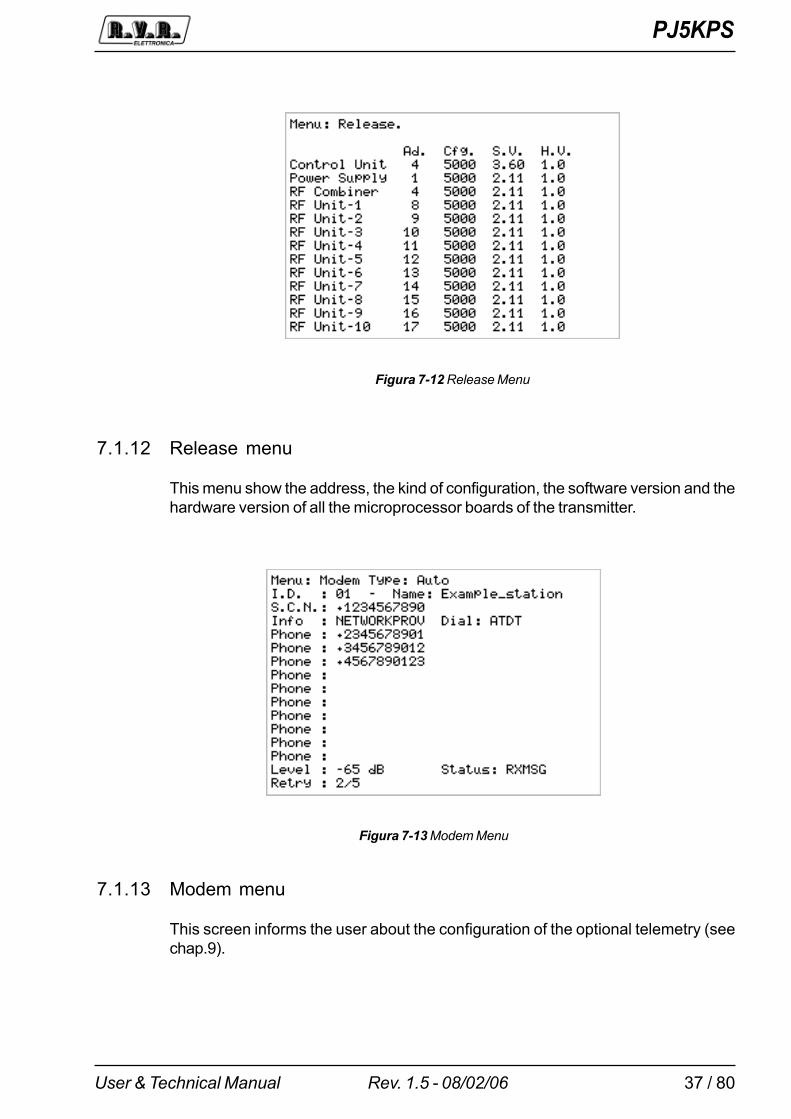
Figura 7-12 Release Menu
7.1.12 Release menu
This menu show the address, the kind of configuration, the software version and thehardware version of all the microprocessor boards of the transmitter.
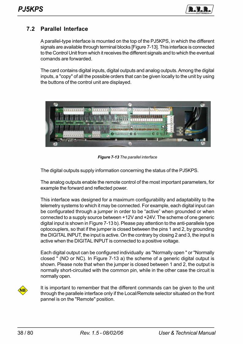
7.1.13 Modem menu
This screen informs the user about the configuration of the optional telemetry (seechap.9).
Figura 7-13 Modem Menu
PJ5KPS
38 / 80 User & Technical ManualRev. 1.5 - 08/02/06
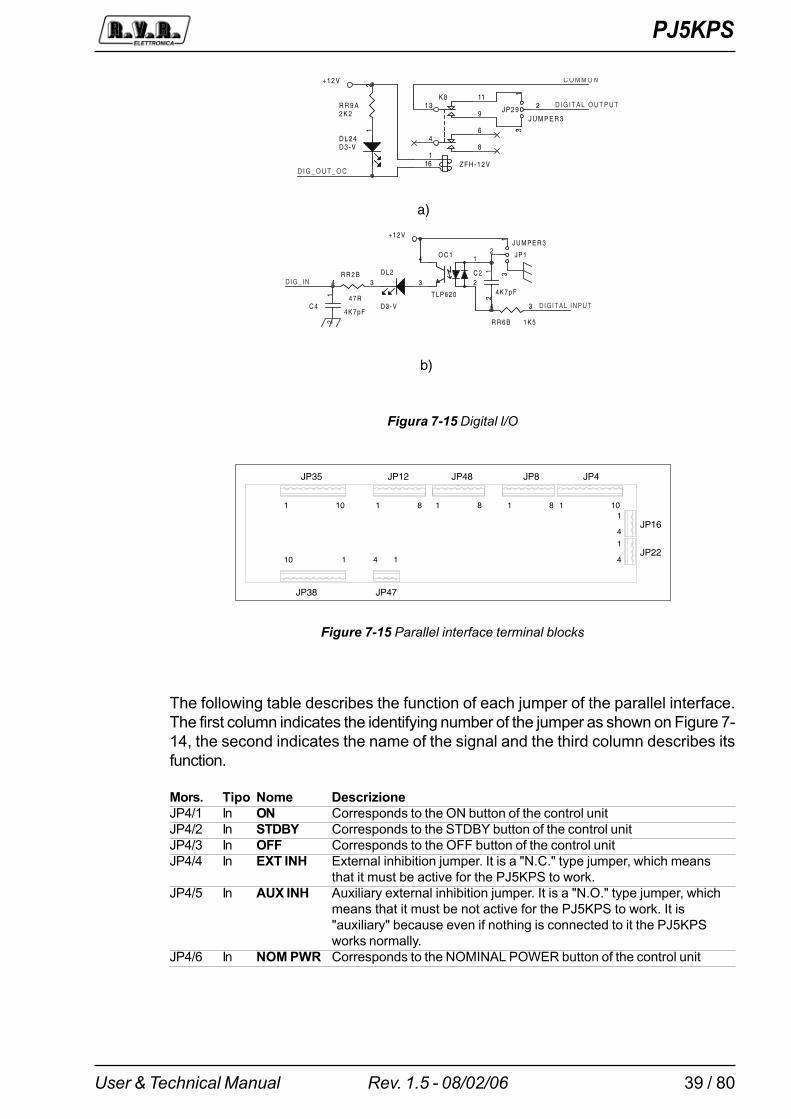
7.2 Parallel Interface
A parallel-type interface is mounted on the top of the PJ5KPS, in which the differentsignals are available through terminal blocks [Figure 7-13]. This interface is connectedto the Control Unit from which it receives the different signals and to which the eventualcomands are forwarded.
The card contains digital inputs, digital outputs and analog outputs. Among the digitalinputs, a "copy" of all the possible orders that can be given locally to the unit by usingthe buttons of the control unit are displayed.
The digital outputs supply information concerning the status of the PJ5KPS.
The analog outputs enable the remote control of the most important parameters, forexample the forward and reflected power.
This interface was designed for a maximum configurability and adaptability to thetelemetry systems to which it may be connected. For example, each digital input canbe configurated through a jumper in order to be �active� when grounded or whenconnected to a supply source between +12V and +24V. The scheme of one genericdigital input is shown in Figure 7-13 b). Please pay attention to the anti-parallele typeoptocouplers, so that if the jumper is closed between the pins 1 and 2, by groundingthe DIGITAL INPUT, the input is active. On the contrary by closing 2 and 3, the input isactive when the DIGITAL INPUT is connected to a positive voltage.
Each digital output can be configured individually as "Normally open " or "Normallyclosed " (NO or NC). In Figure 7-13 a) the scheme of a generic digital output isshown. Please note that when the jumper is closed between 1 and 2, the output isnormally short-circuited with the common pin, while in the other case the circuit isnormally open.
NB It is important to remember that the different commands can be given to the unitthrough the parallele interface only if the Local/Remote selector situated on the frontpannel is on the "Remote" position.
Figure 7-13 The parallel interface
PJ5KPS
39 / 80User & Technical Manual Rev. 1.5 - 08/02/06
The following table describes the function of each jumper of the parallel interface.The first column indicates the identifying number of the jumper as shown on Figure 7-14, the second indicates the name of the signal and the third column describes itsfunction.
Mors. Tipo Nome DescrizioneJP4/1 In ON Corresponds to the ON button of the control unitJP4/2 In STDBY Corresponds to the STDBY button of the control unitJP4/3 In OFF Corresponds to the OFF button of the control unitJP4/4 In EXT INH External inhibition jumper. It is a "N.C." type jumper, which means
that it must be active for the PJ5KPS to work.JP4/5 In AUX INH Auxiliary external inhibition jumper. It is a "N.O." type jumper, which
means that it must be not active for the PJ5KPS to work. It is"auxiliary" because even if nothing is connected to it the PJ5KPSworks normally.
JP4/6 In NOM PWR Corresponds to the NOMINAL POWER button of the control unit
DIGITAL INPUTC 44K7pF
12
R R 2 B
4 7 R
34
+12V
C 2
4K7pF
12
D L 2
D3-V
DIG_ IN
R R 6 B 1K5
34
JP1
J U M P E R 313
2O C 1
TLP620
1
2
4
3
+ 1 2 V C O M M O N
K 8
ZFH-12V
1311
9
46
81
16
JP29J U M P E R 3
13
2R R 9 A2 K 2
12
D I G I T A L O U T P U T
D L 2 4D3-V
D I G _ O U T _ O C
a)
b)
Figura 7-15 Digital I/O
JP4JP8JP48JP12JP35
JP47JP38
JP16
JP22
1 101 81 81 81 10
110 14
1
4
1
4
Figure 7-15 Parallel interface terminal blocks
PJ5KPS
40 / 80 User & Technical ManualRev. 1.5 - 08/02/06
JP4/7 In LOW PWR Corresponds to the REDUCED POWER button of the control unitJP4/8 In AUDIO ALARM EXC. 1
Audio alarm of exciter 1. This input, when active, indicates an alarmon exciter 1. If the PJ5KPS is in automatic changeover modality, ifthe exciter 1 is on air and if this signal remains active for a time lagequivalent to the time setted in the Settings menu at line Exc. Waittime, the changeover procedure between the exciters will be started.
JP4/9 In AUDIO ALARM EXC. 2Same as AUDIO ALARM EXC. 1 for exciter 2.
JP4/10 / GND Grounding contact.JP8/1 In ALARM RESET
Corresponds to the ALARM RESET button on the control unitJP8/2 In RESRV. 1 Reserve 1 input. When this input is active, the failure is registered by
the software in the Alarms menu. For example it can be connected toa switch that indicates that the door of the station is open or to asensor of a power reserve of an electric generator. In this way, byconsulting the menus of the unit, it is possible to trace the moment atwhich (time and date) the failure occured.
JP8/3 In RESRV. 2 Same as JP8/2JP8/4 In RESRV. 3 Same as JP8/2JP8/5 In RESRV. 4 Same as JP8/2JP8/6 In EXCITER CHANGEOVER CMD
This comand launches the changeover procedure between theexciters. It has the same function as when you press the OK buttonwhen selecting line On air exciter in the menu Exciters. In order tolaunch the changeover between the exciters through this comand, themanual changeover modality should be formerly selected through thecorrespondent button on the control unit or through the JP8/7 jumper,having however the unit in "Remote" modality.
JP8/7 In EXCITER CHANGEOVERCorresponds to ther EXCITER CHANGEOVER button of the controlunit
JP8/8 / GND GroundJP16/1 Out +12V dc Power source. A maximum of 100 mA can be absorbed between this
jumper and JP16/2. This power source can be used if the user wantsto enter the comands following a positive logic (high voltage - activecomand)
JP16/2 OUT +12V dc Same as JP16/1JP16/3 / GND GroundJP16/4 / GND GroundJP22/1 I/O TX/RX + Bus RS 485. Please note that this serial port is operational only when
the unit is in "Remote" modality.JP22/2 I/O TX/RX - Bus RS 485JP22/3 / LINE TRM Line termination for bus RS 485JP22/4 / LINE TRM Line termination for bus RS 485JP48/1 / GND GroundJP48/2 / GND GroundJP48/3 Out FWD PWR Forward power. Analogical output, 3.9V for 5000WJP48/4 Out RFL PWR Reflect power. Analogical output, 3.9V for 1200WJP48/5 Out OUT AIR TEMP
Temperature of the air at the output of the chimney. Analogical output,0V for -50°C, 3.9V for 100°C
JP48/6 Out V BUS Voltage at the output of the transformer/rectifier.Analogical output,3.9V for 80V, 0V for 0V.
JP48/7 Out EFF. General efficiency. Analogical output, 3.9V for 100%, 0V for 0%.JP48/8 Out OUT DAC 6 Reserved for future applications.JP12/1 Out CMN MUTE 1
Common contact MUTE 1 (see JP12/2).
PJ5KPS
41 / 80User & Technical Manual Rev. 1.5 - 08/02/06
JP12/2 Out MUTE 1 MUTE excitater 1. Digital output, active when exciter 1 is inhibited bythe control unit. Like all the digital outputs on the parallele interface, itcan be configurated through jumper as normally open or normallyclosed. This output has a common contact dedicated to this function(JP12/1).
JP12/3 Out CMN MUTE 2Common contact MUTE 2 (see JP12/4).
JP12/4 Out MUTE 2 MUTE exciter 2. Digital output, active when exciter 2 is inhibited bythe control unit. This output has a common contact dedicated to thisfunction (JP12/3).
JP12/5 Out CMN LOCALCommon contact LOCAL (see JP12/6).
JP12/6 Out LOCAL LOCAL/REMOTE status. Digital output, active when the PJ5KPS issetted in local modality. This output has a common contact dedicatedto this function (JP12/5).
JP12/7 Out CMN MAINSCommon contact MAINS (see JP12/8).
JP12/8 Out MAINSMAINS alarm, active when are present problems on the alimentation
JP47/1 Out AUDIO ALARM"AUDIO" alarm (see JP4/8 and JP4/9). This output is active when theon air exciter is in audio alarm status. This output has a commoncontact dedicated to this function (JP47/2).
JP47/2 Out CMN AUDIO ALARMCommon contact AUDIO ALARM (see JP47/1).
JP47/3 Out COMMON RL3Common contact shared from the outputs JP38/1-10.
JP47/4 Out COMMON RL3Parallel contact with JP47/3.
JP35/1 Out RESRV. 1 Reserve 1. Digitale output, active when the INPUT RESERVE 1 input(JP8/2) is active. The common contact of this output is RL4 (JP35/5)
JP35/2 Out RESRV. 2 Same as JP35/1, corresponds to INPUT RESERVE 2. The commoncontact of this output RL4 (JP35/5)
JP35/3 Out RESRV. 3 Same as JP35/1, corresponds to INPUT RESERVE 3. The commoncontact of this output RL4 (JP35/5)
JP35/4 Out RESRV. 4 Same as JP35/1, corresponds to INPUT RESERVE 4. The commoncontact of this output RL4 (JP35/5)
JP35/5 Out COMMON RL4Common contact shared between different digital outputs (JP35/1-4)
JP35/6 Out SET1 Digital output, active when the parameter SET1 is active (see menuSettings). The common contact of this output RL5 (JP35/10).
JP35/7 Out SET2 Same as JP36/6, corresponds to SET2. The common contact of thisoutput is RL5 (JP35/10).
JP35/8 Out SET3 Same as JP36/6, corresponds to SET3. The common contact of thisoutput is RL5 (JP35/10).
JP35/9 Out SET4 Similar to JP36/6, related to SET4. The common contact of thisoutput is the RL5 (JP35/10).
JP35/10 Out CMN RL5 Common contact shared between the different digital output (JP35/6-9)
JP38/1 Out EXC. ON AIRDigital output, active when the exciter 1 is on air, and not active whenthe exciter 2 is on air. common contact of this output is the RL3(JP47/3).
JP38/2 Out AUTO/MAN Digital output, active when the PJ5KPS is in changeover mode asregards the exciters . The common contact of this output is RL3(JP47/3).
JP38/3 Out LOWER POWERDigital output, active when the PJ5KPS is set for the lower powerlevel. Common contact of this output is the RL3 (JP47/3).
JP38/4 Out NOMINAL POWERDigital output, active when the PJ5KPS is set for the nominal power

PJ5KPS
42 / 80 User & Technical ManualRev. 1.5 - 08/02/06
level. common contact of this output is the RL3 (JP47/3).JP38/5 Out OFF Digital output, active when the PJ5KPS is set for the lower power
level. The common contact of this output is the RL3 (JP47/3).JP38/6 Out STDBY Digital output, active when the PJ5KPS is set for the lower power
level. The common contact of this output is the RL3 (JP47/3).JP38/7 Out ON Digital output, active when the PJ5KPS is set on ON mode . The
common contact of this output is the RL3 (JP47/3).JP38/8 Out FAULT Digital output, active when the PJ5KPS is set on FAULT mode . The
common contact of this output is the RL3 (JP47/3).JP38/9 Out WAIT Digital output, active when the PJ5KPS is set on WAIT mode. The
common contact of this output is the RL3 (JP47/3).JP38/10 Out WARNING Digital output, active when the PJ5KPS is set on WARNING mode .
The common contact of this output is the RL3 (JP47/3).
7.3 Power supply section
The power supply used by the PJ5KPS is AC threephase with neutral at 380 V. Thepower supply for the RF amplifier modules is DC 80 V, stabilized inside the modulesthemselves by a built-in switching power supply.
The power supply section of the PJ5KPS is composed of a threephase transformerand a rectifier circuit to feed the RF modules. Some features of the power supplysection are the following:
� PF > 0.94. This value of the power factor is got thanks to specific solutions, suchas power inductors use. The result is a wave shape of the absorbed currentparticularly cleaned and meeting the requirements of the most demanding users.
� Redundancy. Where an uninterrupted service is demanded, is possible to add asecond power supply chart. The functionning of the max power output is warrantiedby a power supply only, so the double power supply use allow to be used as backup in case of fault of one of them.
� Easy access. The power supply section is located on a chart with wheels for aneasy take out from the cabinet and easy transportation. When the configuration ofthe equipment is with double power supply chart is possible to stop (take out andservice) a section without turn off the equipment.
� The power supply section of the PJ5KPS is checked by a microprocessor cardincluded in the rack of the equipment . This card manages one or two more powersupply charts , the cooling blower and the several alarms systems such as theemergency "not aus" button.
7.3.1 Working Principles
The Power Supply is checked by a microprocessor unit completely indipendent inthe alarming functions and activity respect to the control unit. The interchanges signalsbetween the two units are present on a flat cable of 20 poles named �datacommunication and command bus�. The signals present on the bus that are relatedto the power supply section are: ON, Stby, Alarm, Tr+/Tr-.
PJ5KPS
43 / 80User & Technical Manual Rev. 1.5 - 08/02/06
Signal FunctionON When the control of the power supply section notices a +12V on this
signal, the start up cicled of the power supply carriages is activated.The cicle is divided in two phases: the first contactor enables the powertransformer through power resistors, so that the possible current peakat start-up is reduced; two seconds later, the second contactor isexcited, so that the transformer is directly fed. After an additional delayof a second, the first contactor is released.At this point, the start-up cicle is terminated and the STDBY line isreleased.
STDBY When this signal is at ground, the RF modules are forced on a RF mutemode. The power supply section maintain on a stand-by position thecontrol bus untill the start-up cicle is ended, or when the ON signal isnot present, or at the end in all the coditions that are controlled by thissection that can affect the safety of the equipment. When all thechecked conditions are satisfactory the signal is released.
Alarm When this signal is at ground the control unit checks all the devicespresent on the bus to register and and manage eventual alarms. Whena signal or an alarm that affect the power supply section is revealed,the processor that is used to control it orders to the line to go down soto communicate to the control unit the event.
Tr+/Tr- These signals are used for data communication. The levels meet RS485standard , the speed is 115 kb/s. Please note that an eventual failure onthese signals doesn't affect the complex functionning of the equipment.
Figure 7-16 Time chart of the carriages contactors
Bus Command Soft-Startcontactor
StartContactor
FanContactor
STDBYOutput
OFF 0 0 0 ActiveSTDBY 0 1 1 Not ActiveON 0 1 1 Not Active
Table 7-1 Time chart of the carriages contactors
PJ5KPS
44 / 80 User & Technical ManualRev. 1.5 - 08/02/06
In addition to the contactors that permit the soft-start function, this unit control thecooling blower function. This is switched on together with the On command, while,when the equipment is in OFF mode, the blower relay stops to be driven after about4 minutes. This laboursaving device is used to avoid that temperature peaks to bepresent at the internal of RF modules. This procedure of post-ventilation is used forall conditions of equipment stops, both in case of human will or in case of alarm .
Table 7.1 contains a schematic of the output of the power supply section. The graphicdisplay of the contactor status during the time is reported in the Picture 7-16.
7.3.2 Configurations
The power supply section of the PJ5KPS has the following configuration possibilities:
1 Equipment with single power supply carriage
2 Equipment with double power supply carriage
3 Equipment with automatic reset of the Safety function at the emergency buttonrelease
4 Equipment with reset of the Safety function to be done manually by pushing thebutton.
The standard configuration of the equipment includes the points 1 and 3.
7.3.3 Logic control Signals
The power supply section of the PJ5KPS constantly controls the logic signals thatcan be divided in general signals (related to the equipment in its complex) or carriagessignals (related to the single power supply carriages). The status of these signalscan be checked on the Power Supply Menu in the control unit.
When a fault is detected in one of the general signals, the PJ5KPS is blocked eithertemporarily blocked or until the intervention of the maintenance staff, depending onthe type of signal. The general signals with relative meaning and managing modeare the following:
Signal FunctionSafety This signal in alarm status when the emergency button is pushed. In
this case the feed line to the several contactors is immediatelysectioned, per cui si ha un arresto istantaneo di tutte le parti soggette apotenza; the exciters remain however operational.In the meantime a signal send a message to the control local unit of thecurrent conditions. To restore the funtionning of the equipment theemergency button has to be reload.; if the equipment is configurate inmode 3), the start-up cicle is activated after two seconds. If the powersupply is configurated in mode 4) it will be necessary to push theSAFETY RESET button to restart the equipment. The safety signal isnot memorized on the events menu.
PJ5KPS
45 / 80User & Technical Manual Rev. 1.5 - 08/02/06
Mains This signal is generated by an external device that control that thepower supply current meets the limits of the functionning and that theR,S,T direction of progression of the phases is correct. If the mains ison alarm status, The equipment stops working , including the feeding ofthe exciters. When the signal return , an automatic restart occurs. Allthe time that an alarm of this type is present , a relative message in themenu alarm of the control unit is memorized.
Air pressure A pressure sensor informs the local unit if the cooling air flow is notcorrect ; the intervention of the sensor stops the equipment temporarilywith the disconnection of the power supply contactors of the powertransformers . When the signal returns an automatic restart of thePJ5KPS takes place. An opportune message is memorized in theAlarm menu in the control unit of the unit all the times that this signalinterveens.
Blower Motor Protector The intervention of the ground protection of the motor protector put theequipment on Fault mode. This condition requires the presence of anoperator to restore the functionning of the equipment . In order toattempt to restart it's necessary to reload the motor protector and pushthe ALARMS RESET of the control unit . Each time that this signalinterveens an opportune message is memorized in the alarm menu ofthe control unit.
The �carriage signals� are related to the status of the single carriages. A possiblealarm status in one of these signals has a different effect on the transmitter dependingon the number of the included power supply carriages, single or dual. While in thefirst case the PJ5KPS is stopped in case of a fault, in the second case the sparecarriages is still able to supply all the required power; in this case the fault is signaledby the LED Warning on the front panel.
The meanings of the carriage signals are the following:
Signal FunctionFuse 1 This signal, meaning �Carriage 1 Fuse� signal is in fact composed of the
series of all the safety interlocks of the carriage. If this signal is in thealarm status, it will be necessary to determine which of the followingpossible reasons is causing it: AC power fuse, microswitch of the chartconnected. The magneto-thermic switch , command connector coils,control signals connector , threephase power connector.
Trafo 1 OH This signal, meaning "Overheating transformer 1" (Trafo 1 Over Heat), isconnected to the safety thermal switches. There are two differentsensors: one is on the transformer lamelIar plate, the other is on therectifier heat dissipator. The intervention of one of these two devicesstops temporarily the equipment on WAIT mode. When temperaturegoes below the threshold, the transmitter will automatically restart.The temperature of intervention is 90°C, and in case this alarm arises, itwill be recorded with a message in the alarm menu on the control unit.
Fuse 2 As Fuse 1, for carriage 2Trafo 2 OH As Trafo 1 OH, for carriage 2
If the signal Fuse X is on alarm, in order to restore the regular functionning of theequipment it is necessary to identify the cause of the fault. The following table resumesthe points to be verified in order to find the cause of malfunctionning :
PJ5KPS
46 / 80 User & Technical ManualRev. 1.5 - 08/02/06
Signal ConditionPower fuse Verify that the LED on the rectifier card is switched off
[Figure7-18]Chart microswitch Verify that the power supply carriage is perfectly attached to the
bottom and that pushes the microswitch [Figure 7-17 b)]Magneto-thermic chart Switch Verify that the switch is on position I [Figure 7-17 a)]Control signals connectors Verify that the plug is connected in the right way [Figure 7-18]Command coils connector Verify that the plug is connected in the right way [Figure 7-18]Three-phase power connector Verify that the plug is connected in the right way [Figure 7-17 a)]
Note that the handle on the left side of the connector has to bepulled toward the front of the transmitter to block the connector inits place.
7.3.4 Control card
The functions of this microprocessor card are the following :
� Protection of the power supply section
� Communication with the control unit
� Analog parameters measurement
The card is installed in the rack under the RF modules site, in a metallic box whereit's included the control card of RF combiner [Figure 7-18 a)]. This card needs twoanalogic tunings : air input temperature and Bus DC voltage (not stabilized). For thetuning use the Power Supply menu of the control unit and identify the appropriatetrimmers in Figure [7-18 b)].
All the input digital signals are of "PNP" type, the common power supply is 12Vdc;the line of 12 Vdc is protected against the ground short circuit through a self-restoringfuse (ptc). An possible short circuit on this supply will cause trip the machine. Eventualmessages of fault in corrispondence of a short circuit on this line won't be valid.
To restore the supply is necessary to remove the short circuit condition and switchOFF the equipment for about a minute in order to let the fuse self-restore.
7.3.5 Interface Board
The control card of the power supply is connected with the actuators through aninterface board [Figure 7-19].
All the output signals from the control card are interfaced through power relays andsignal relays. On the relay coils a signalling LED is present and indicates the commandstatus on the control unit: the LED turned ON indicates that the coil is excited. All thepower contacts are equipped with noise suppressing network.
The feeding of the relay is supplied from a line protected against the short circuitthrough self-reloading ground protections.

PJ5KPS
47 / 80User & Technical Manual Rev. 1.5 - 08/02/06
AC powerfuse
Bus-bar Vdc visualization Fuse
Control signalsconnector
Relays commandconnector
Fuse memoryreset button
Fuse interventionLED
Figura 7-18 Rectifiers board check points
a) b)
Figura 7-17 Carriages check points
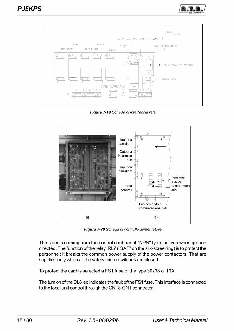
PJ5KPS
48 / 80 User & Technical ManualRev. 1.5 - 08/02/06
The signals coming from the control card are of "NPN" type, actives when grounddirected. The function of the relay RL7 ("SAF" on the silk-screening) is to protect thepersonnel: it breaks the common power supply of the power contactors, That aresupplied only when all the safety micro-switches are closed.
To protect the card is selected a FS1 fuse of the type 30x38 of 10A.
The turn on of the DL8 led indicates the fault of the FS1 fuse. This interface is connectedto the local unit control through the CN18-CN1 connector.
Figura 7-19 Scheda di interfaccia relè
Temperaturaaria
TensioneBus bar
Input dacarrello 1
Input dacarrello 2
Output ainterfacca
relè
Inputgenerali
Bus comando ecomunicazione dati
a) b)
Figura 7-20 Scheda di controllo alimentatore
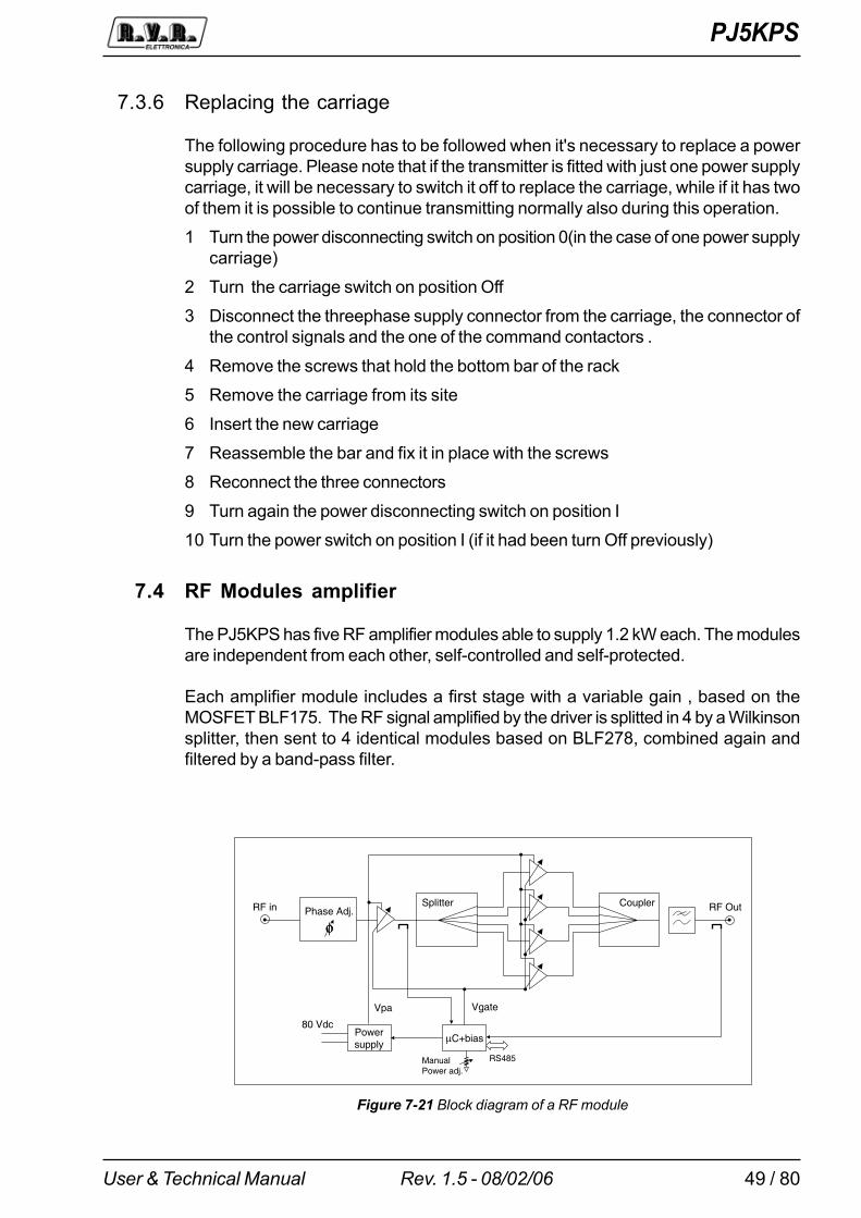
PJ5KPS
49 / 80User & Technical Manual Rev. 1.5 - 08/02/06
7.3.6 Replacing the carriage
The following procedure has to be followed when it's necessary to replace a powersupply carriage. Please note that if the transmitter is fitted with just one power supplycarriage, it will be necessary to switch it off to replace the carriage, while if it has twoof them it is possible to continue transmitting normally also during this operation.
1 Turn the power disconnecting switch on position 0(in the case of one power supplycarriage)
2 Turn the carriage switch on position Off
3 Disconnect the threephase supply connector from the carriage, the connector ofthe control signals and the one of the command contactors .
4 Remove the screws that hold the bottom bar of the rack
5 Remove the carriage from its site
6 Insert the new carriage
7 Reassemble the bar and fix it in place with the screws
8 Reconnect the three connectors
9 Turn again the power disconnecting switch on position I
10 Turn the power switch on position I (if it had been turn Off previously)
7.4 RF Modules amplifier
The PJ5KPS has five RF amplifier modules able to supply 1.2 kW each. The modulesare independent from each other, self-controlled and self-protected.
Each amplifier module includes a first stage with a variable gain , based on theMOSFET BLF175. The RF signal amplified by the driver is splitted in 4 by a Wilkinsonsplitter, then sent to 4 identical modules based on BLF278, combined again andfiltered by a band-pass filter.
RF in
80 Vdc
Splitter Coupler
Powersupply
RF Out
RS485
Phase Adj.
φφ
μC+bias
Vpa
ManualPower adj.
Vgate
Figure 7-21 Block diagram of a RF module
PJ5KPS
50 / 80 User & Technical ManualRev. 1.5 - 08/02/06
Each RF amplifier module is controlled by a microprocessor card, connected througha RS485 bus to the other microprocessor cards of the machine.
The switching power supply included in each amplifier module generates the feedingsupply of the active devices. The generated voltage is adjustable and commandedby a microprocessor card included in the module. The card adjusts the supply andthe polarization current (gate) of the modules, thus controlling the emitted power.
On each module there is a trimmer for the manual adjustment of the power. Thetrimmer acts as a limiter. This means that if the automatic adjustment of the powersets a nominal output value, the trimmer can only reduce it, and not increase it.
7.5 Alarms
The menu Alarms of the control unit reports all the events connected to possiblemalfunctionning of the equipment or due to external causes.
Each registration contains the reference to the concerned module, the kind of eventand its date and hour.
The module that detected the event is indicated by one of the following acronyms:� C.U. Control Unit� P.S. Power Supply� R.F.X Amplifier module X (from 1 to 5)� R.F.C Combiner/Splitter
The type of event allows to identify the origin and the consequence of the fault. Thefirst letter of the type of event (eg F-C.B. Blw) can be one of the following :
E "Error", event that doesn't cause the interruption of the supply of power,but can reduce the functions of the equipment (e.g cannot be done thechangeover function of the exciters)
F "Fault", event that causes the block of the equipment and requires theintervention of an operator for the restart.
W "Wait", event that causes the temporary block of the piece of equipmentequipment, that will be removed as soon as the problem is solved.
R "Retry", event that causes a temporary block of the piece of equipment,that will effect a restart attempt after a fixed lapse of time.
The possible type of events are listed in Table 7-2
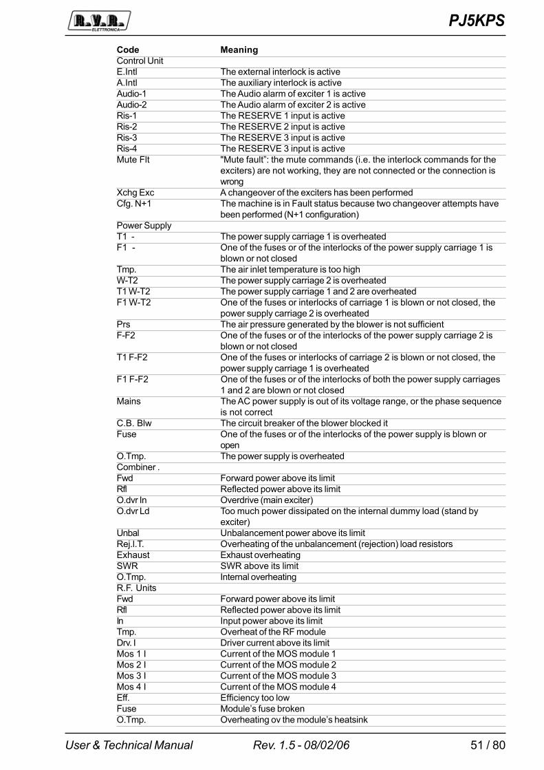
PJ5KPS
51 / 80User & Technical Manual Rev. 1.5 - 08/02/06
Code MeaningControl UnitE.Intl The external interlock is activeA.Intl The auxiliary interlock is activeAudio-1 The Audio alarm of exciter 1 is activeAudio-2 The Audio alarm of exciter 2 is activeRis-1 The RESERVE 1 input is activeRis-2 The RESERVE 2 input is activeRis-3 The RESERVE 3 input is activeRis-4 The RESERVE 3 input is activeMute Flt "Mute fault�: the mute commands (i.e. the interlock commands for the
exciters) are not working, they are not connected or the connection iswrong
Xchg Exc A changeover of the exciters has been performedCfg. N+1 The machine is in Fault status because two changeover attempts have
been performed (N+1 configuration)Power SupplyT1 - The power supply carriage 1 is overheatedF1 - One of the fuses or of the interlocks of the power supply carriage 1 is
blown or not closedTmp. The air inlet temperature is too highW-T2 The power supply carriage 2 is overheatedT1 W-T2 The power supply carriage 1 and 2 are overheatedF1 W-T2 One of the fuses or interlocks of carriage 1 is blown or not closed, the
power supply carriage 2 is overheatedPrs The air pressure generated by the blower is not sufficientF-F2 One of the fuses or of the interlocks of the power supply carriage 2 is
blown or not closedT1 F-F2 One of the fuses or interlocks of carriage 2 is blown or not closed, the
power supply carriage 1 is overheatedF1 F-F2 One of the fuses or of the interlocks of both the power supply carriages
1 and 2 are blown or not closedMains The AC power supply is out of its voltage range, or the phase sequence
is not correctC.B. Blw The circuit breaker of the blower blocked itFuse One of the fuses or of the interlocks of the power supply is blown or
openO.Tmp. The power supply is overheatedCombiner .Fwd Forward power above its limitRfl Reflected power above its limitO.dvr In Overdrive (main exciter)O.dvr Ld Too much power dissipated on the internal dummy load (stand by
exciter)Unbal Unbalancement power above its limitRej.l.T. Overheating of the unbalancement (rejection) load resistorsExhaust Exhaust overheatingSWR SWR above its limitO.Tmp. Internal overheatingR.F. UnitsFwd Forward power above its limitRfl Reflected power above its limitIn Input power above its limitTmp. Overheat of the RF moduleDrv. I Driver current above its limitMos 1 I Current of the MOS module 1Mos 2 I Current of the MOS module 2Mos 3 I Current of the MOS module 3Mos 4 I Current of the MOS module 4Eff. Efficiency too lowFuse Module�s fuse brokenO.Tmp. Overheating ov the module�s heatsink
PJ5KPS
52 / 80 User & Technical ManualRev. 1.5 - 08/02/06
7.6 Combiner and divider
7.6.1 Control Unit
The RF combiner section too is equipped with it own microprocessor control unit.This is very important for the functionning of the whole transmitter because it checksthe foldback line of the several RF modules. The value of the output power is manageddirectly by this micro controller. In case of fault of this control unit or if a problemarises in the communication bus, the transmitter will continue working at the samepower level set in the field "nominal power" of the control unit.
To this unit is assigned the task to limitate and stabilize the output power. When oneof the parameters reaches its safety limit for the right functionning of the machine, thepower level decreases progressively. The feedback is completely of analogic type,made through a voltage present on the control bus. The voltage is between themaximum of 3.9 V (this indicates that the transmitter is supplying the maximum power)and 0 V (minimum power).
This section also controls the maximum permitted power level of the exciters, with aprogrammed alarm of �Fault� type. If this level is exceeded the transmitter turns itselfOFF and the AC supply of the exciters is cut until the operator pushes the AlarmsReset button.
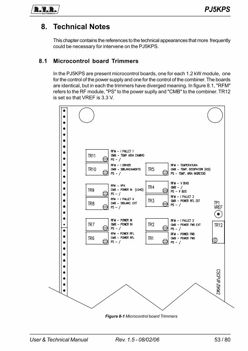
PJ5KPS
53 / 80User & Technical Manual Rev. 1.5 - 08/02/06
8. Technical NotesThis chapter contains the references to the technical appearances that more frequentlycould be necessary for intervene on the PJ5KPS.
8.1 Microcontrol board Trimmers
In the PJ5KPS are present microcontrol boards, one for each 1.2 kW module, onefor the control of the power supply and one for the control of the combiner. The boardsare identical, but in each the trimmers have diverged meaning. In figure 8.1, "RFM"refers to the RF module, "PS" to the power suplly and "CMB" to the combiner. TR12is set so that VREF is 3.3 V.
Figure 8-1 Microcontrol board Trimmers
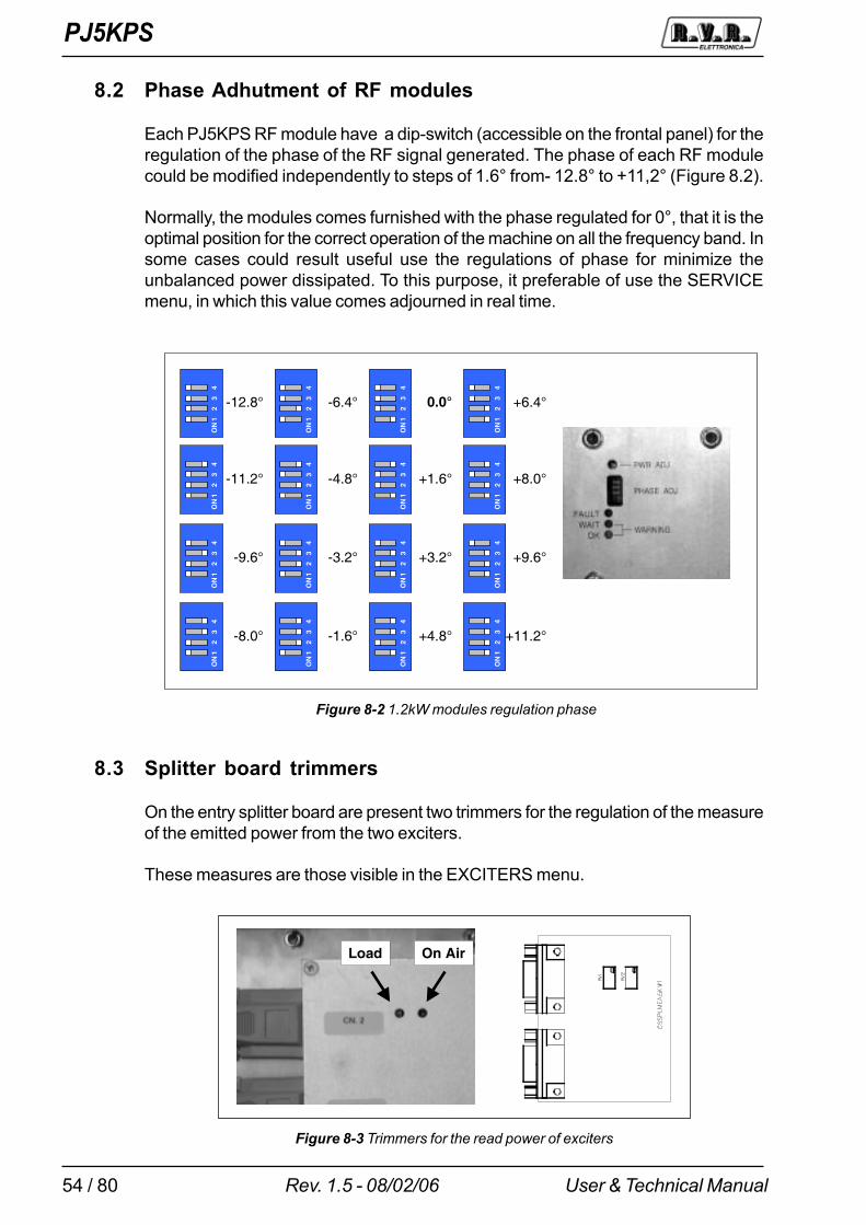
PJ5KPS
54 / 80 User & Technical ManualRev. 1.5 - 08/02/06
8.2 Phase Adhutment of RF modules
Each PJ5KPS RF module have a dip-switch (accessible on the frontal panel) for theregulation of the phase of the RF signal generated. The phase of each RF modulecould be modified independently to steps of 1.6° from- 12.8° to +11,2° (Figure 8.2).
Normally, the modules comes furnished with the phase regulated for 0°, that it is theoptimal position for the correct operation of the machine on all the frequency band. Insome cases could result useful use the regulations of phase for minimize theunbalanced power dissipated. To this purpose, it preferable of use the SERVICEmenu, in which this value comes adjourned in real time.
8.3 Splitter board trimmers
On the entry splitter board are present two trimmers for the regulation of the measureof the emitted power from the two exciters.
These measures are those visible in the EXCITERS menu.
12
34
ON
-12.8°
12
34
ON
-11.2°
12
34
ON
-9.6°
12
34
ON
-8.0°
12
34
ON
-6.4°
12
34
ON
-4.8°
12
34
ON
-3.2°
12
34
ON
-1.6°
12
34
ON
0.0°1
23
4O
N
+1.6°
12
34
ON
+3.2°
12
34
ON
+4.8°
12
34
ON
+6.4°
12
34
ON
+8.0°1
23
4O
N
+9.6°
12
34
ON
+11.2°
Figure 8-2 1.2kW modules regulation phase
Load On Air
Figure 8-3 Trimmers for the read power of exciters
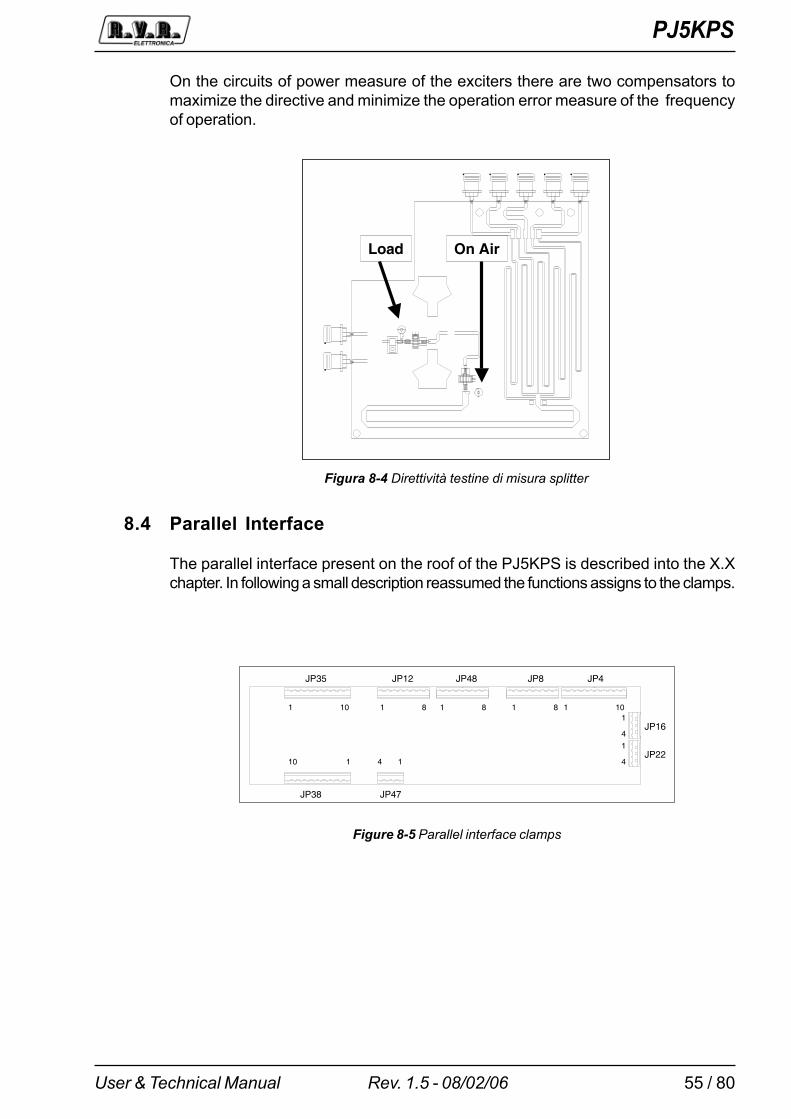
PJ5KPS
55 / 80User & Technical Manual Rev. 1.5 - 08/02/06
On the circuits of power measure of the exciters there are two compensators tomaximize the directive and minimize the operation error measure of the frequencyof operation.
8.4 Parallel Interface
The parallel interface present on the roof of the PJ5KPS is described into the X.Xchapter. In following a small description reassumed the functions assigns to the clamps.
Load On Air
Figura 8-4 Direttività testine di misura splitter
JP4JP8JP48JP12JP35
JP47JP38
JP16
JP22
1 101 81 81 81 10
110 14
1
4
1
4
Figure 8-5 Parallel interface clamps
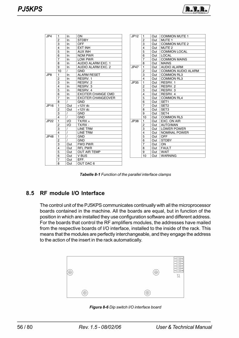
PJ5KPS
56 / 80 User & Technical ManualRev. 1.5 - 08/02/06
1 In ON 1 Out COMMON MUTE 12 In STDBY 2 Out MUTE 13 In OFF 3 Out COMMON MUTE 24 In EXT INH 4 Out MUTE 25 In AUX INH 5 Out COMMON LOCAL6 In NOM PWR 6 Out LOCAL7 In LOW PWR 7 Out COMMON MAINS8 In AUDIO ALARM EXC. 1
JP12
8 Out MAINS9 In AUDIO ALARM EXC. 2 1 Out AUDIO ALARM
JP4
10 / GND 2 Out COMMON AUDIO ALARM1 In ALARM RESET 3 Out COMMON RL32 In RESRV. 1
JP47
4 Out COMMON RL33 In RESRV. 2 1 Out RESRV. 14 In RESRV. 3 2 Out RESRV. 25 In RESRV. 4 3 Out RESRV. 36 In EXCITER CHANGE CMD 4 Out RESRV. 47 In EXCITER CHANGEOVER 5 Out COMMON RL4
JP8
8 / GND 6 Out SET11 Out +12V dc 7 Out SET22 Out +12V dc 8 Out SET33 / GND 9 Out SET4
JP16
4 / GND
JP35
10 Out COMMON RL51 I/O TX/RX + 1 Out EXC. ON AIR2 I/O TX/RX - 2 Out AUTO/MAN3 / LINE TRM 3 Out LOWER POWER
JP22
4 / LINE TRM 4 Out NOMINAL POWER1 / GND 5 Out OFF2 / GND 6 Out STDBY3 Out FWD PWR 7 Out ON4 Out RFL PWR 8 Out FAULT5 Out OUT AIR TEMP 9 Out WAIT6 Out V BUS
JP38
10 Out WARNING7 Out EFF.
JP48
8 Out OUT DAC 6
Tabelle 8-1 Function of the parallel interface clamps
8.5 RF module I/O Interface
The control unit of the PJ5KPS communicates continually with all the microprocessorboards contained in the machine. All the boards are equal, but in function of theposition in which are installed they use configuration software and different address.For the boards that control the RF amplifiers modules, the addresses have mailedfrom the respective boards of I/O interface, installed to the inside of the rack. Thismeans that the modules are perfectly interchangeable, and they engage the addressto the action of the insert in the rack automatically.
Figura 8-6 Dip switch I/O interface board
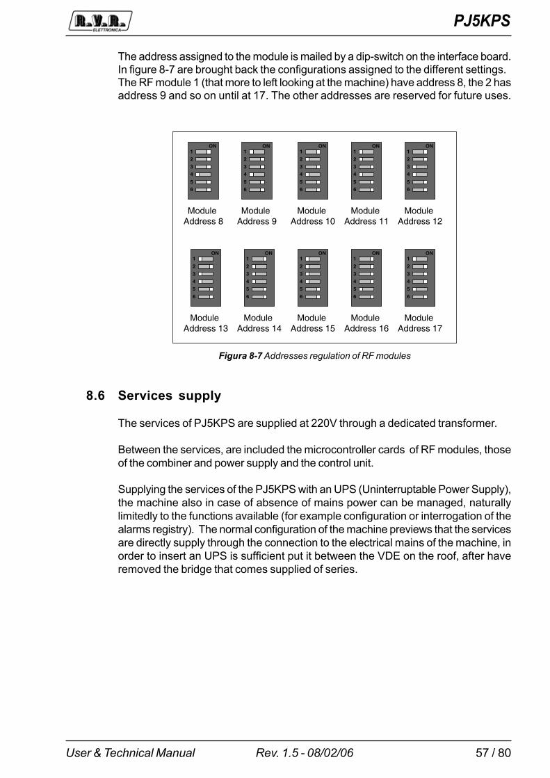
PJ5KPS
57 / 80User & Technical Manual Rev. 1.5 - 08/02/06
8.6 Services supply
The services of PJ5KPS are supplied at 220V through a dedicated transformer.
Between the services, are included the microcontroller cards of RF modules, thoseof the combiner and power supply and the control unit.
Supplying the services of the PJ5KPS with an UPS (Uninterruptable Power Supply),the machine also in case of absence of mains power can be managed, naturallylimitedly to the functions available (for example configuration or interrogation of thealarms registry). The normal configuration of the machine previews that the servicesare directly supply through the connection to the electrical mains of the machine, inorder to insert an UPS is sufficient put it between the VDE on the roof, after haveremoved the bridge that comes supplied of series.
1ON
2
3
4
5
6
Module Address 8
1ON
2
3
4
5
6
Module Address 9
1ON
2
3
4
5
6
Module Address 10
1ON
2
3
4
5
6
Module Address 11
1ON
2
3
4
5
6
Module Address 12
1ON
2
3
4
5
6
Module Address 13
1ON
2
3
4
5
6
Module Address 14
1ON
2
3
4
5
6
Module Address 15
1ON
2
3
4
5
6
Module Address 16
1ON
2
3
4
5
6
Module Address 17
Figura 8-7 Addresses regulation of RF modules
The address assigned to the module is mailed by a dip-switch on the interface board.In figure 8-7 are brought back the configurations assigned to the different settings.The RF module 1 (that more to left looking at the machine) have address 8, the 2 hasaddress 9 and so on until at 17. The other addresses are reserved for future uses.

PJ5KPS
58 / 80 User & Technical ManualRev. 1.5 - 08/02/06
Figure 8-8 Services supply
8.7 Emergency CCU Board
In the case the control unit presents a damage, it is possible assure the correctoperation replacing, temporarily, the control panel with the card furnished togetherwith the PJ5KPS.
To effect the substitution, execute the following instructions:
1) Switch-OFF the amplifier. Remove the screw on the left side of the LCD panel,open the panel and individualize the necessary connectors to the operation of theemergency card.
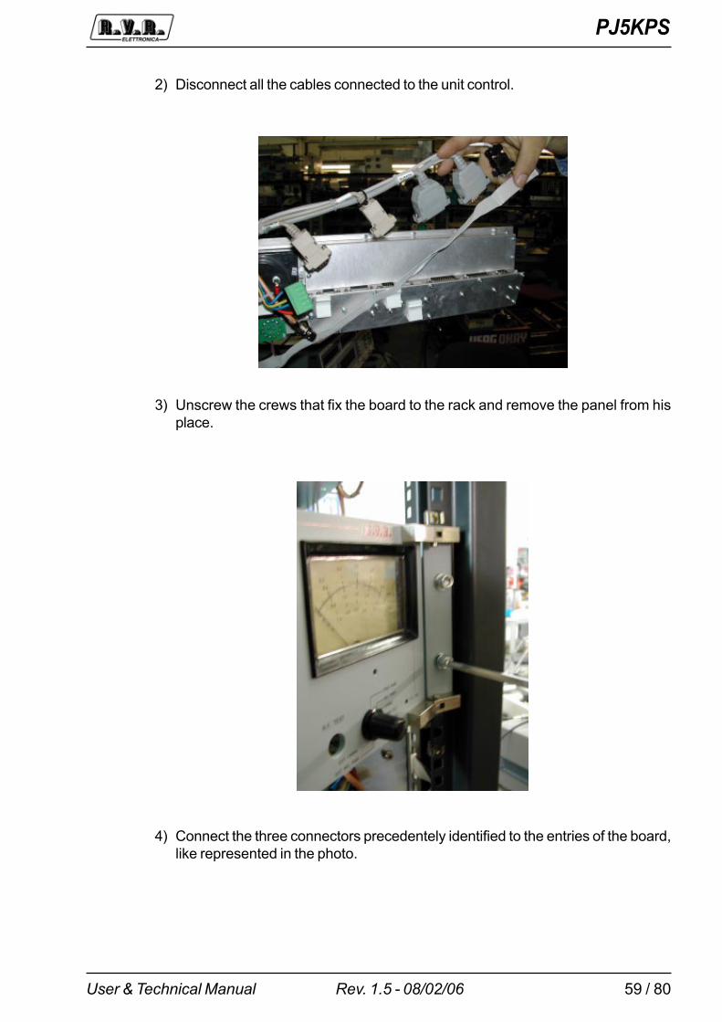
PJ5KPS
59 / 80User & Technical Manual Rev. 1.5 - 08/02/06
2) Disconnect all the cables connected to the unit control.
3) Unscrew the crews that fix the board to the rack and remove the panel from hisplace.
4) Connect the three connectors precedentely identified to the entries of the board,like represented in the photo.
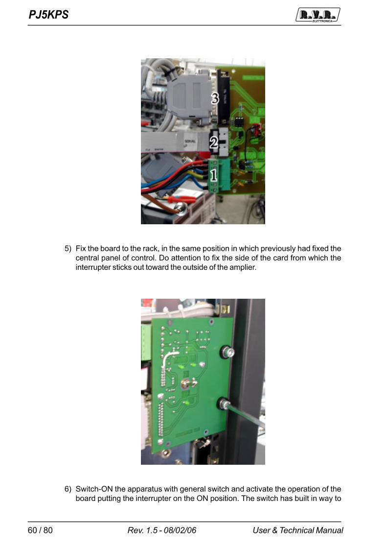
PJ5KPS
60 / 80 User & Technical ManualRev. 1.5 - 08/02/06
5) Fix the board to the rack, in the same position in which previously had fixed thecentral panel of control. Do attention to fix the side of the card from which theinterrupter sticks out toward the outside of the amplier.
6) Switch-ON the apparatus with general switch and activate the operation of theboard putting the interrupter on the ON position. The switch has built in way to
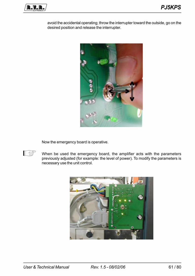
PJ5KPS
61 / 80User & Technical Manual Rev. 1.5 - 08/02/06
avoid the accidental operating; throw the interrupter toward the outside, go on thedesired position and release the interrupter.
Now the emergency board is operative.
When be used the emergency board, the amplifier acts with the parameterspreviously adjusted (for example: the level of power). To modify the parameters isnecessary use the unit control.
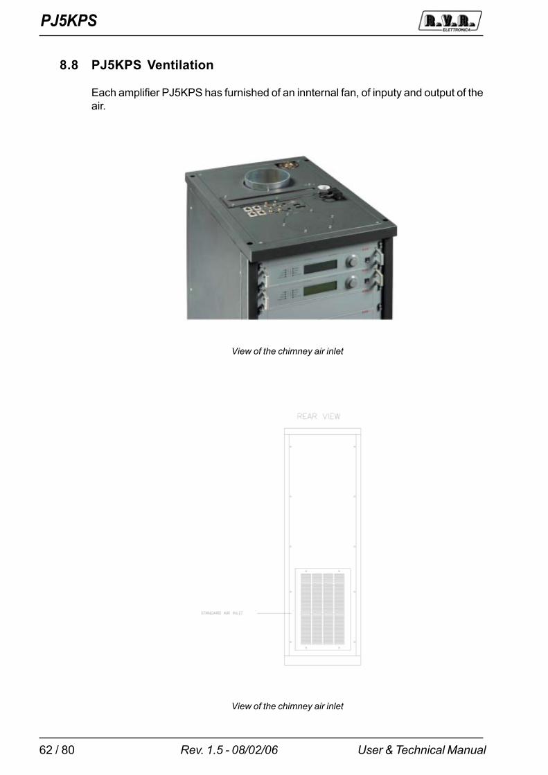
PJ5KPS
62 / 80 User & Technical ManualRev. 1.5 - 08/02/06
8.8 PJ5KPS Ventilation
Each amplifier PJ5KPS has furnished of an innternal fan, of inputy and output of theair.
View of the chimney air inlet
View of the chimney air inlet
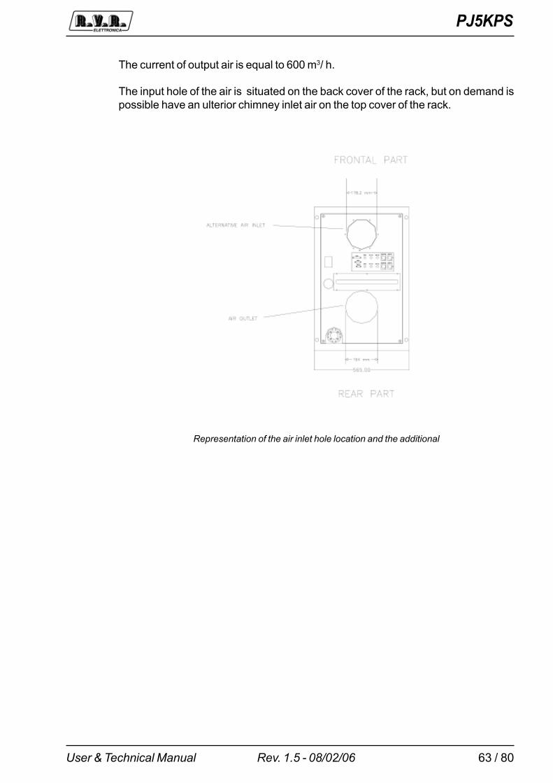
PJ5KPS
63 / 80User & Technical Manual Rev. 1.5 - 08/02/06
The current of output air is equal to 600 m3/ h.
The input hole of the air is situated on the back cover of the rack, but on demand ispossible have an ulterior chimney inlet air on the top cover of the rack.
Representation of the air inlet hole location and the additional
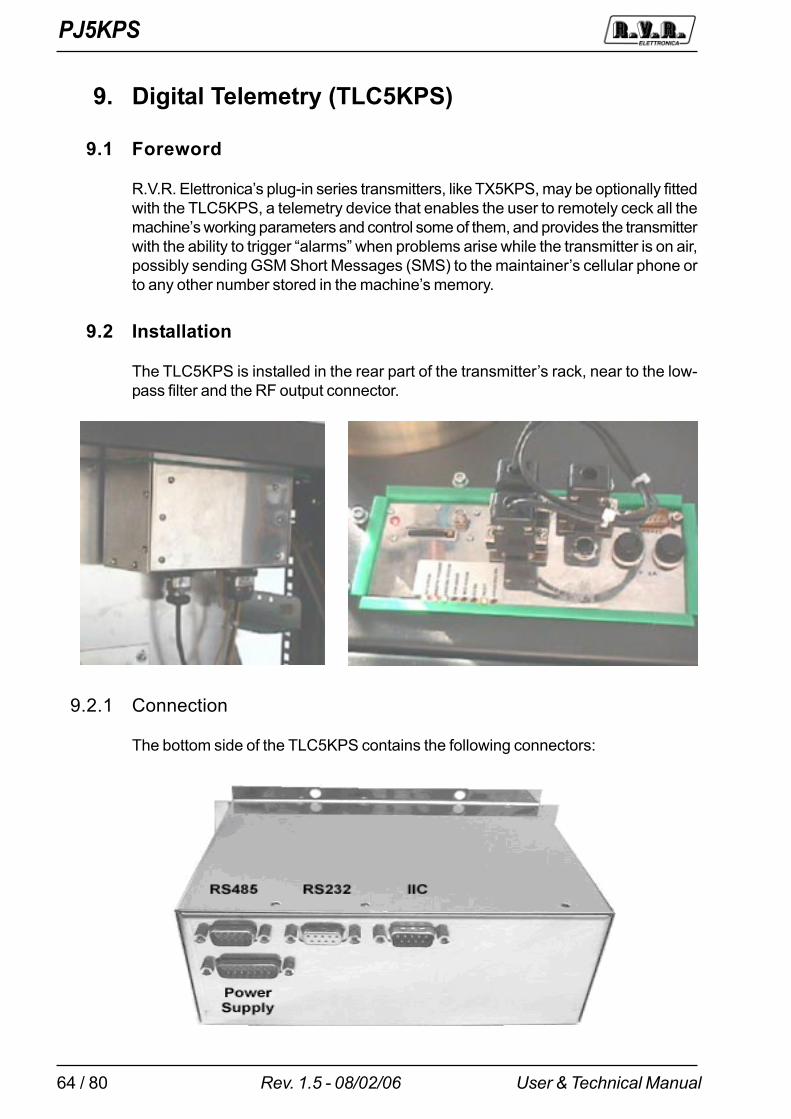
PJ5KPS
64 / 80 User & Technical ManualRev. 1.5 - 08/02/06
9. Digital Telemetry (TLC5KPS)
9.1 Foreword
R.V.R. Elettronica�s plug-in series transmitters, like TX5KPS, may be optionally fittedwith the TLC5KPS, a telemetry device that enables the user to remotely ceck all themachine�s working parameters and control some of them, and provides the transmitterwith the ability to trigger �alarms� when problems arise while the transmitter is on air,possibly sending GSM Short Messages (SMS) to the maintainer�s cellular phone orto any other number stored in the machine�s memory.
9.2 Installation
The TLC5KPS is installed in the rear part of the transmitter�s rack, near to the low-pass filter and the RF output connector.
9.2.1 Connection
The bottom side of the TLC5KPS contains the following connectors:
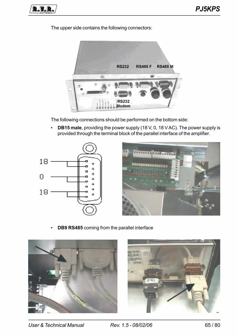
PJ5KPS
65 / 80User & Technical Manual Rev. 1.5 - 08/02/06
The upper side contains the following connectors:
The following connections should be performed on the bottom side:
� DB15 male, providing the power supply (18 V, 0, 18 V AC). The power supply isprovided through the terminal block of the parallel interface of the amplifier.
� DB9 RS485 coming from the parallel interface
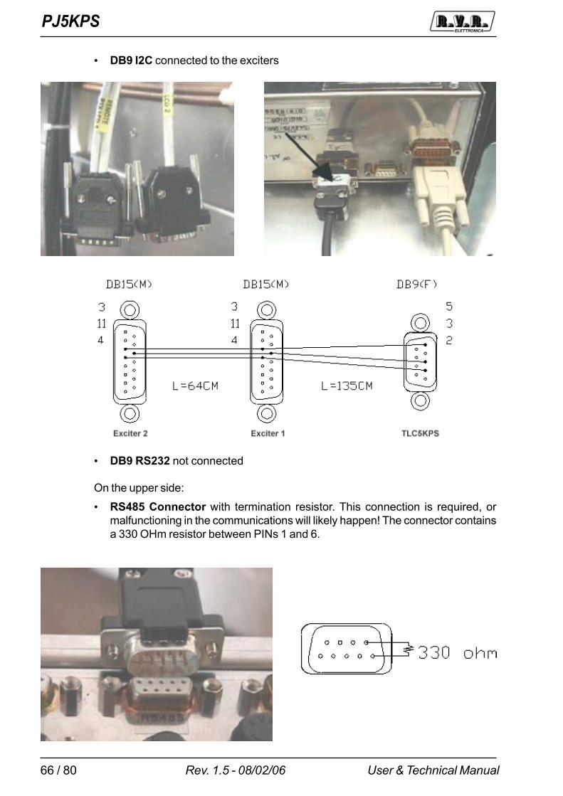
PJ5KPS
66 / 80 User & Technical ManualRev. 1.5 - 08/02/06
� DB9 I2C connected to the exciters
� DB9 RS232 not connected
On the upper side:
� RS485 Connector with termination resistor. This connection is required, ormalfunctioning in the communications will likely happen! The connector containsa 330 OHm resistor between PINs 1 and 6.
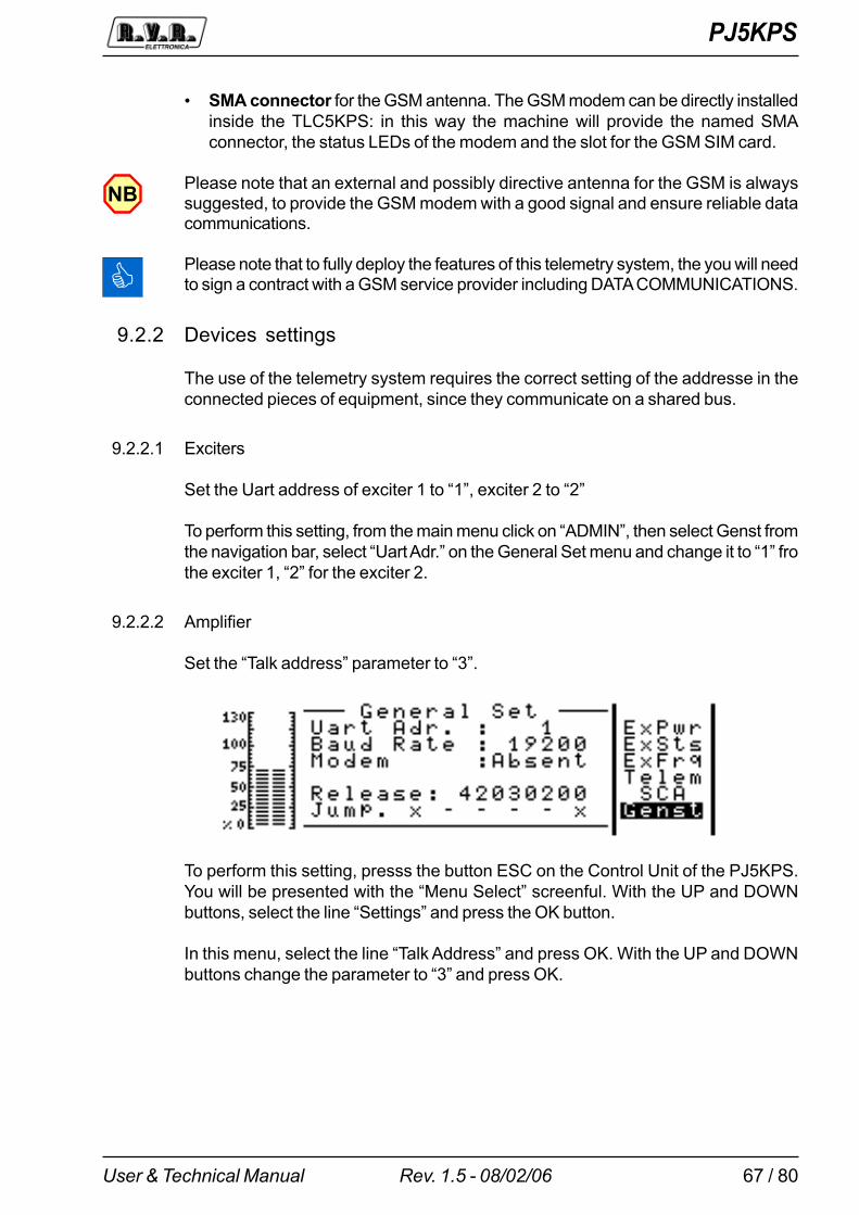
PJ5KPS
67 / 80User & Technical Manual Rev. 1.5 - 08/02/06
� SMA connector for the GSM antenna. The GSM modem can be directly installedinside the TLC5KPS: in this way the machine will provide the named SMAconnector, the status LEDs of the modem and the slot for the GSM SIM card.
Please note that an external and possibly directive antenna for the GSM is alwayssuggested, to provide the GSM modem with a good signal and ensure reliable datacommunications.
Please note that to fully deploy the features of this telemetry system, the you will needto sign a contract with a GSM service provider including DATA COMMUNICATIONS.
9.2.2 Devices settings
The use of the telemetry system requires the correct setting of the addresse in theconnected pieces of equipment, since they communicate on a shared bus.
9.2.2.1 Exciters
Set the Uart address of exciter 1 to �1�, exciter 2 to �2�
To perform this setting, from the main menu click on �ADMIN�, then select Genst fromthe navigation bar, select �Uart Adr.� on the General Set menu and change it to �1� frothe exciter 1, �2� for the exciter 2.
9.2.2.2 Amplifier
Set the �Talk address� parameter to �3�.
To perform this setting, presss the button ESC on the Control Unit of the PJ5KPS.You will be presented with the �Menu Select� screenful. With the UP and DOWNbuttons, select the line �Settings� and press the OK button.
In this menu, select the line �Talk Address� and press OK. With the UP and DOWNbuttons change the parameter to �3� and press OK.
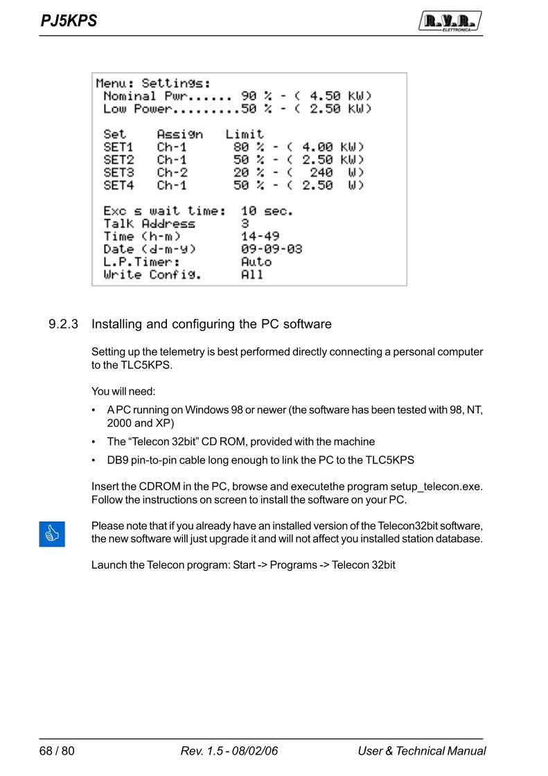
PJ5KPS
68 / 80 User & Technical ManualRev. 1.5 - 08/02/06
9.2.3 Installing and configuring the PC software
Setting up the telemetry is best performed directly connecting a personal computerto the TLC5KPS.
You will need:
� A PC running on Windows 98 or newer (the software has been tested with 98, NT,2000 and XP)
� The �Telecon 32bit� CD ROM, provided with the machine
� DB9 pin-to-pin cable long enough to link the PC to the TLC5KPS
Insert the CDROM in the PC, browse and executethe program setup_telecon.exe.Follow the instructions on screen to install the software on your PC.
Please note that if you already have an installed version of the Telecon32bit software,the new software will just upgrade it and will not affect you installed station database.
Launch the Telecon program: Start -> Programs -> Telecon 32bit
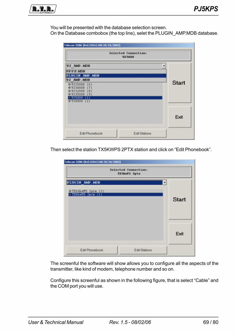
PJ5KPS
69 / 80User & Technical Manual Rev. 1.5 - 08/02/06
You will be presented with the database selection screen.On the Database combobox (the top line), selet the PLUGIN_AMP.MDB database.
Then select the station TX5KWPS 2PTX station and click on �Edit Phonebook�.
The screenful the software will show allows you to configure all the aspects of thetransmitter, like kind of modem, telephone number and so on.
Configure this screenful as shown in the following figure, that is select �Cable� andthe COM port you will use.
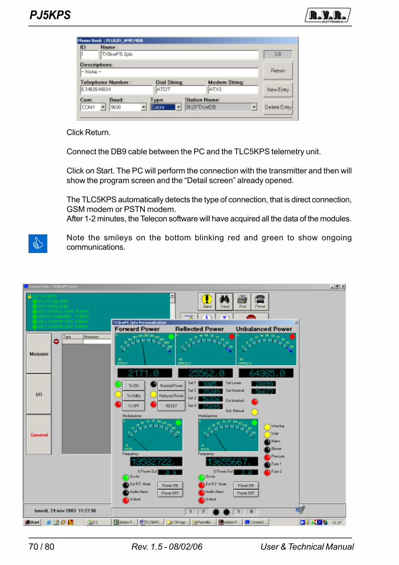
PJ5KPS
70 / 80 User & Technical ManualRev. 1.5 - 08/02/06
Click Return.
Connect the DB9 cable between the PC and the TLC5KPS telemetry unit.
Click on Start. The PC will perform the connection with the transmitter and then willshow the program screen and the �Detail screen� already opened.
The TLC5KPS automatically detects the type of connection, that is direct connection,GSM modem or PSTN modem.After 1-2 minutes, the Telecon software will have acquired all the data of the modules.
Note the smileys on the bottom blinking red and green to show ongoingcommunications.
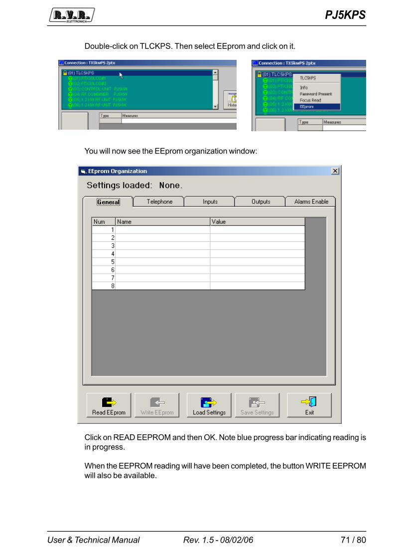
PJ5KPS
71 / 80User & Technical Manual Rev. 1.5 - 08/02/06
Double-click on TLCKPS. Then select EEprom and click on it.
You will now see the EEprom organization window:
Click on READ EEPROM and then OK. Note blue progress bar indicating reading isin progress.
When the EEPROM reading will have been completed, the button WRITE EEPROMwill also be available.
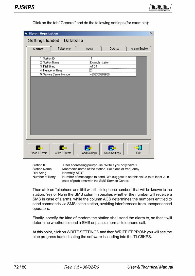
PJ5KPS
72 / 80 User & Technical ManualRev. 1.5 - 08/02/06
Click on the tab �General� and do the following settings (for example):
Station ID ID for addressing pourpouse. Write if you only have 1Station Name Mnemonic name of the station, like place or frequencyDial Sring Normally, ATDTNumber of Retry Number of messages to send. We suggest to set this value to at least 2, in
case of problems with the SMS Service Center.
Then click on Telephone and fill it with the telephone numbers that will be known to thestation. Yes or No in the SMS column specifies whether the number will receive aSMS in case of alarms, while the column ACS determines the numbers entitled tosend commands via SMS to the station, avoiding interferences from unexperiencedoperators.
Finally, specify the kind of modem the station shall send the alarm to, so that it willdetermine whether to send a SMS or place a normal telephone call.
At this point, click on WRITE SETTINGS and then WRITE EEPROM: you will see theblue progress bar indicating the software is loading into the TLC5KPS.
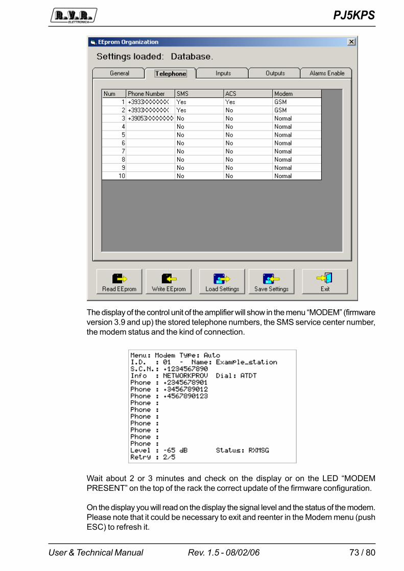
PJ5KPS
73 / 80User & Technical Manual Rev. 1.5 - 08/02/06
The display of the control unit of the amplifier will show in the menu �MODEM� (firmwareversion 3.9 and up) the stored telephone numbers, the SMS service center number,the modem status and the kind of connection.
Wait about 2 or 3 minutes and check on the display or on the LED �MODEMPRESENT� on the top of the rack the correct update of the firmware configuration.
On the display you will read on the display the signal level and the status of the modem.Please note that it could be necessary to exit and reenter in the Modem menu (pushESC) to refresh it.
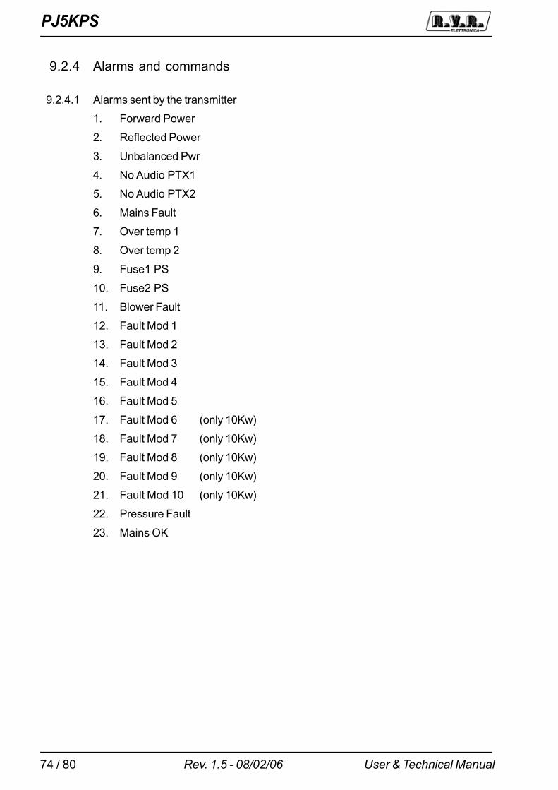
PJ5KPS
74 / 80 User & Technical ManualRev. 1.5 - 08/02/06
9.2.4 Alarms and commands
9.2.4.1 Alarms sent by the transmitter
1. Forward Power
2. Reflected Power
3. Unbalanced Pwr
4. No Audio PTX1
5. No Audio PTX2
6. Mains Fault
7. Over temp 1
8. Over temp 2
9. Fuse1 PS
10. Fuse2 PS
11. Blower Fault
12. Fault Mod 1
13. Fault Mod 2
14. Fault Mod 3
15. Fault Mod 4
16. Fault Mod 5
17. Fault Mod 6 (only 10Kw)
18. Fault Mod 7 (only 10Kw)
19. Fault Mod 8 (only 10Kw)
20. Fault Mod 9 (only 10Kw)
21. Fault Mod 10 (only 10Kw)
22. Pressure Fault
23. Mains OK

PJ5KPS
75 / 80User & Technical Manual Rev. 1.5 - 08/02/06
9.2.4.2 SMS commands available
The commands that can be sent to the transmitter using SMS messages are thefollowing:
The Alarms for the RF power falling under a certain level and for the reflected powerare connected to the Settings menu. Remember to adjust SET 1 SET2 and SET 3 inthis menu to suit your need.
When all of these parameters have beenfinally configured, put the selector on thecontrol panel of the control unit on the �Remote� position. The yellow �LOCAL� led willgo off and the green led will go on. We suggest at this point to do some tests to verifythe functionality of the system.
�������� �� � �����������
INFO
Station: ������������ID: � ������� FWD: �������� RFL: ��������UNBAL:������� TX On (�� TX Off �� TX StdBy)- Low Power / Nom Power Audio Present / Audio Absent Alarm Present / Alarm Absent
Information about the transmitter�s status
TXON Station: ������������ID: � ������� TX is On -
Switching on the transmitter
TXOFF Station: ������������ID: � ������� TX is Off
Switching off the transmitter
LOWPWR Station: ������������ID: � ������� LowPwr OK-
Low Power setting
NOMPWR Station: ������������ID: � ������� NomPwr OK-
Nominal Power setting
ALARM Station: ������������ID: � ������� Alarm: ����������������������
List of the alarms in memory
RESET Station: ������������ID: � ������� ALARM RESET OK-
Resetting the alarms in memory
RESMOD -- nothing -- Reset of the telemetry and modem restart
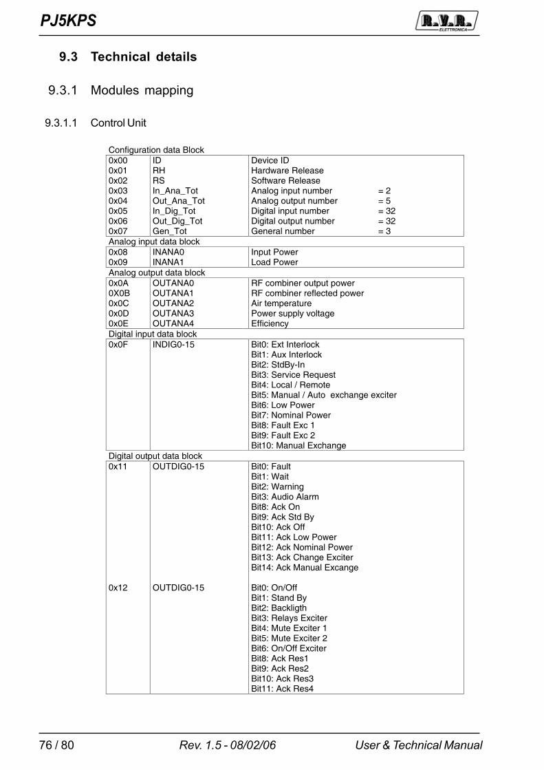
PJ5KPS
76 / 80 User & Technical ManualRev. 1.5 - 08/02/06
9.3 Technical details
9.3.1 Modules mapping
9.3.1.1 Control Unit
Configuration data Block 0x00 0x01 0x02 0x03 0x04 0x05 0x06 0x07
ID RH RS In_Ana_Tot Out_Ana_Tot In_Dig_Tot Out_Dig_Tot Gen_Tot
Device ID Hardware Release Software Release Analog input number = 2 Analog output number = 5 Digital input number = 32 Digital output number = 32 General number = 3
Analog input data block 0x08 0x09
INANA0 INANA1
Input Power Load Power
Analog output data block 0x0A 0X0B 0x0C 0x0D 0x0E
OUTANA0 OUTANA1 OUTANA2 OUTANA3 OUTANA4
RF combiner output power RF combiner reflected power Air temperature Power supply voltage Efficiency
Digital input data block 0x0F
INDIG0-15 Bit0: Ext Interlock Bit1: Aux Interlock Bit2: StdBy-In Bit3: Service Request Bit4: Local / Remote Bit5: Manual / Auto exchange exciter Bit6: Low Power Bit7: Nominal Power Bit8: Fault Exc 1 Bit9: Fault Exc 2 Bit10: Manual Exchange
Digital output data block 0x11 0x12
OUTDIG0-15 OUTDIG0-15
Bit0: Fault Bit1: Wait Bit2: Warning Bit3: Audio Alarm Bit8: Ack On Bit9: Ack Std By Bit10: Ack Off Bit11: Ack Low Power Bit12: Ack Nominal Power Bit13: Ack Change Exciter Bit14: Ack Manual Excange Bit0: On/Off Bit1: Stand By Bit2: Backligth Bit3: Relays Exciter Bit4: Mute Exciter 1 Bit5: Mute Exciter 2 Bit6: On/Off Exciter Bit8: Ack Res1 Bit9: Ack Res2 Bit10: Ack Res3 Bit11: Ack Res4
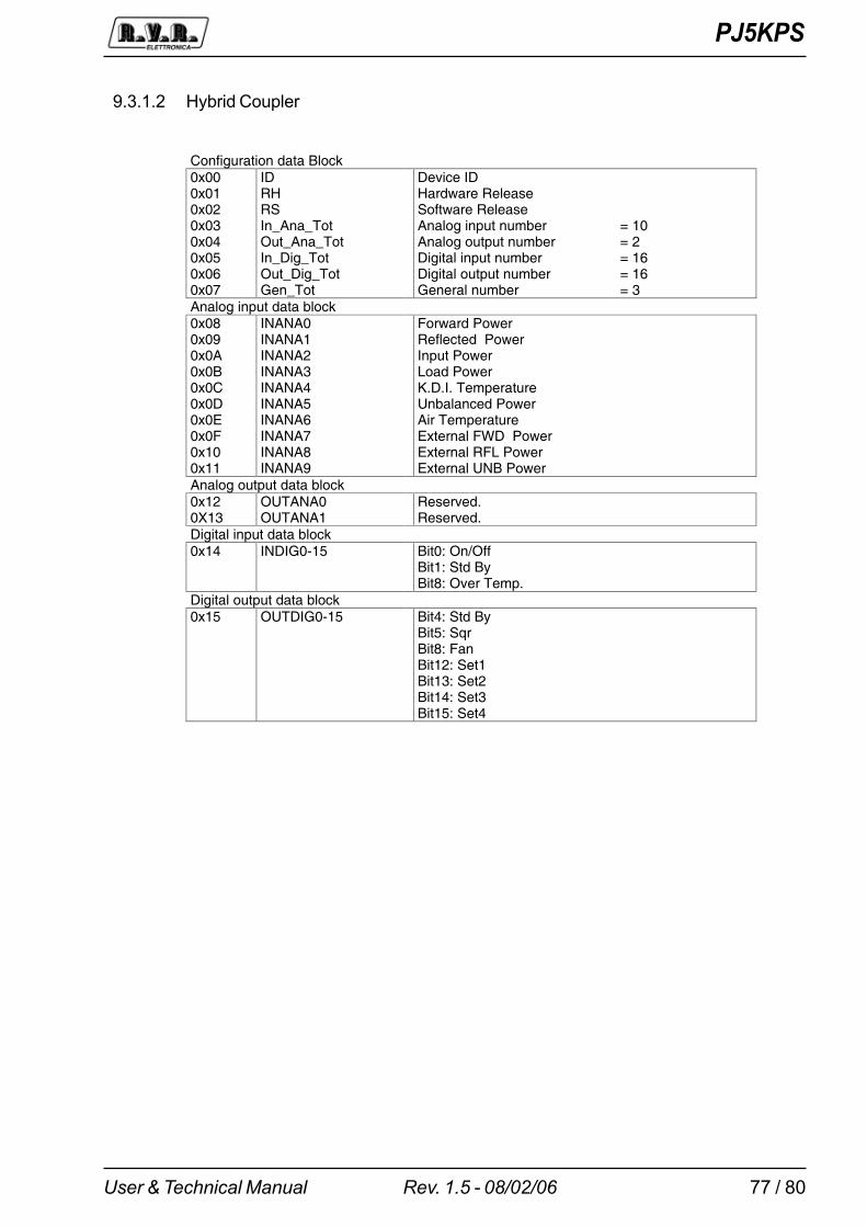
PJ5KPS
77 / 80User & Technical Manual Rev. 1.5 - 08/02/06
9.3.1.2 Hybrid Coupler
Configuration data Block 0x00 0x01 0x02 0x03 0x04 0x05 0x06 0x07
ID RH RS In_Ana_Tot Out_Ana_Tot In_Dig_Tot Out_Dig_Tot Gen_Tot
Device ID Hardware Release Software Release Analog input number = 10 Analog output number = 2 Digital input number = 16 Digital output number = 16 General number = 3
Analog input data block 0x08 0x09 0x0A 0x0B 0x0C 0x0D 0x0E 0x0F 0x10 0x11
INANA0 INANA1 INANA2 INANA3 INANA4 INANA5 INANA6 INANA7 INANA8 INANA9
Forward Power Reflected Power Input Power Load Power K.D.I. Temperature Unbalanced Power Air Temperature External FWD Power External RFL Power External UNB Power
Analog output data block 0x12 0X13
OUTANA0 OUTANA1
Reserved. Reserved.
Digital input data block 0x14
INDIG0-15
Bit0: On/Off Bit1: Std By Bit8: Over Temp.
Digital output data block 0x15
OUTDIG0-15
Bit4: Std By Bit5: Sqr Bit8: Fan Bit12: Set1 Bit13: Set2 Bit14: Set3 Bit15: Set4
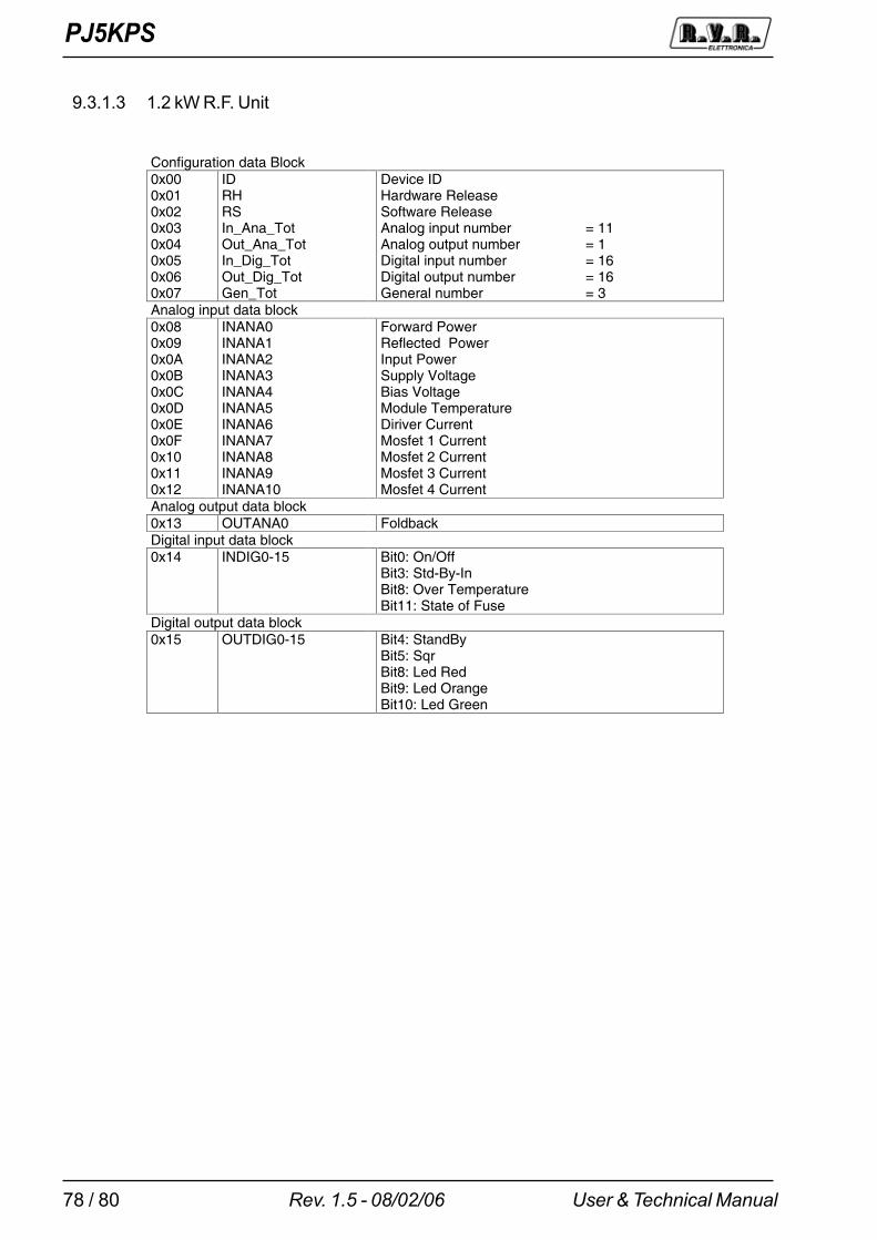
PJ5KPS
78 / 80 User & Technical ManualRev. 1.5 - 08/02/06
9.3.1.3 1.2 kW R.F. Unit
Configuration data Block 0x00 0x01 0x02 0x03 0x04 0x05 0x06 0x07
ID RH RS In_Ana_Tot Out_Ana_Tot In_Dig_Tot Out_Dig_Tot Gen_Tot
Device ID Hardware Release Software Release Analog input number = 11 Analog output number = 1 Digital input number = 16 Digital output number = 16 General number = 3
Analog input data block 0x08 0x09 0x0A 0x0B 0x0C 0x0D 0x0E 0x0F 0x10 0x11 0x12
INANA0 INANA1 INANA2 INANA3 INANA4 INANA5 INANA6 INANA7 INANA8 INANA9 INANA10
Forward Power Reflected Power Input Power Supply Voltage Bias Voltage Module Temperature Diriver Current Mosfet 1 Current Mosfet 2 Current Mosfet 3 Current Mosfet 4 Current
Analog output data block 0x13 OUTANA0 Foldback Digital input data block 0x14
INDIG0-15
Bit0: On/Off Bit3: Std-By-In Bit8: Over Temperature Bit11: State of Fuse
Digital output data block 0x15
OUTDIG0-15
Bit4: StandBy Bit5: Sqr Bit8: Led Red Bit9: Led Orange Bit10: Led Green
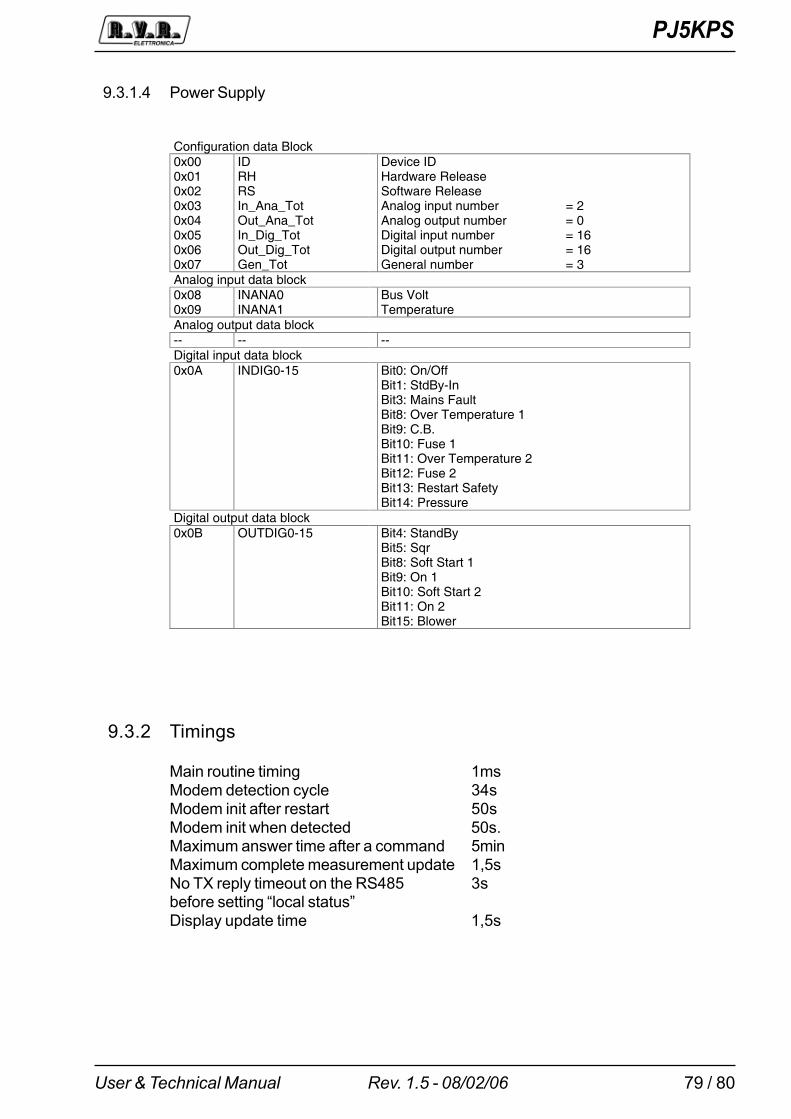
PJ5KPS
79 / 80User & Technical Manual Rev. 1.5 - 08/02/06
9.3.1.4 Power Supply
Configuration data Block 0x00 0x01 0x02 0x03 0x04 0x05 0x06 0x07
ID RH RS In_Ana_Tot Out_Ana_Tot In_Dig_Tot Out_Dig_Tot Gen_Tot
Device ID Hardware Release Software Release Analog input number = 2 Analog output number = 0 Digital input number = 16 Digital output number = 16 General number = 3
Analog input data block 0x08 0x09
INANA0 INANA1
Bus Volt Temperature
Analog output data block -- -- -- Digital input data block 0x0A
INDIG0-15
Bit0: On/Off Bit1: StdBy-In Bit3: Mains Fault Bit8: Over Temperature 1 Bit9: C.B. Bit10: Fuse 1 Bit11: Over Temperature 2 Bit12: Fuse 2 Bit13: Restart Safety Bit14: Pressure
Digital output data block 0x0B
OUTDIG0-15
Bit4: StandBy Bit5: Sqr Bit8: Soft Start 1 Bit9: On 1 Bit10: Soft Start 2 Bit11: On 2 Bit15: Blower
9.3.2 Timings
Main routine timing 1msModem detection cycle 34sModem init after restart 50sModem init when detected 50s.Maximum answer time after a command 5minMaximum complete measurement update 1,5sNo TX reply timeout on the RS485 3sbefore setting �local status�Display update time 1,5s

PJ5KPS
80 / 80 User & Technical ManualRev. 1.5 - 08/02/06
This page was intentionally left blank

1 / 2User & Technical ManualTechnical Appendix
Rev. 1.5 - 08/02/06
PJ5KPS
Appendix A Piani di montaggio, schemi elettrici, listecomponenti / Component layouts,schematics, bills of material
Questa parte del manuale contiene i dettagli tecnici riguardanti la costruzione dellesingole schede componenti del PJ5KPS. L�appendice è composta dalle seguentisezioni:
This part of the manual contains the technical details about the different boards ofthe PJ5KPS LCD. This appendix is composed of the following sections:
Descrizione Codice RVR Vers. Pagg.Modulo RF SL042RF1001 1.1 3 (A4)Accoppiatore direzionale modulo RF SLDCLPFPJ1KM 1.1 3 (A4)Misure splitter ingresso SLSPLMEA5KW1 1.0 3 (A4)Splitter modulo RF SLSPLRFPJ5KM 1.0 3 (A4)Scheda fusibili modulo RF SLFUSRFPJ5KM 1.0 3 (A4)Scheda misura sbilanciamento SLPWRSENHC52 1.0 3 (A4)Selettore misura analogica SLMETPJ5KM4 1.0 3 (A4)Interfaccia I/O modulo RF SLIORFPJ5KM2 1.1 3 (A4)Accoppiatore direzionale di uscita SL042MT1001 1.0 3 (A4)Interfaccia relè di potenza SLRLYCPROTVJ 1.0 3 (A4)Emergency CCU SLCCUEMPJ5K2 1.0 3 (A4)Schema del cablaggio / 1.1 1 (A3)Scheda microcontrollore SLCPUPJ5KM2 1.0 7 (A3)Adattatore CPU PS e combinatore SLADPPSPJ5KM2 1.0 4 (A3)Rettificatore trifase SLRCTPJ5KMC 1.1 3 (A3)Scheda CPU control unit SLCCUPJ5KM2 1.0 6 (A3)Scheda madre control unit SLCCU1PJ5KM2 1.0 3 (A3)Interfaccia parallela SLINTREMPJ5KM 1.0 4 (A3)Splitter/scambiatore ingresso SLSPLINPJ5KW1 1.0 3 (A3)Scheda CPU misura sbilanciamento SLADKDIPJ5K2 1.0 3 (A3)Adattatore CPU/bias modulo RF SLADBSPJ5KM2 1.1 5 (A3)Driver modulo RF SLDRVRFPJ5M 1.0 3 (A3)Alimentatore switching modulo RF PSSW5040 1.2 5 (A3)
2 / 2 Manuale d�uso e manutenzioneAppendice tecnica
Rev. 1.5 - 08/02/06
PJ5KPS
Pagina lasciata intenzionalmente in biancoThis page intentionally left blank

Appendix to the user manual© 2002 -2006 R.V.R. Elettronica SpA - All rights reserved
RF Amplifier module - SL042RF1001
PJ5KPS
1 / 3
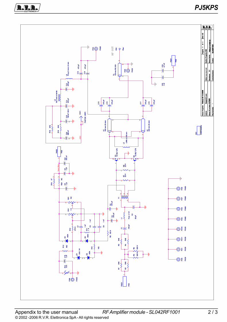
Appendix to the user manual© 2002 -2006 R.V.R. Elettronica SpA - All rights reserved
RF Amplifier module - SL042RF1001
PJ5KPS
2 / 3
Inpu
t_B
ias
+50V
No
me P
rog
ett
o:
Au
tore
:C
od
ice P
rog
ett
o:
No
me P
C i
n R
ete
:
Fil
e/
Cart
ell
a:
Data
:
Revis
ion
e:
Co
dic
e:
No
me P
art
e:
Au
tori
zzazi
on
e:
Pag
ina:
Siz
e:
di
\\UTS
RVFI
NALE
PJ1
000
6U
SL04
2RF1
001
1.1
FINA
LE R
F PJ
1000
M
042
Gas
perin
i Luc
a
11
A3
Mon
day,
Oct
ober
03,
200
5
/
No
me P
rog
ett
o:
Au
tore
:C
od
ice P
rog
ett
o:
No
me P
C i
n R
ete
:
Fil
e/
Cart
ell
a:
Data
:
Revis
ion
e:
Co
dic
e:
No
me P
art
e:
Au
tori
zzazi
on
e:
Pag
ina:
Siz
e:
di
\\UTS
RVFI
NALE
PJ1
000
6U
SL04
2RF1
001
1.1
FINA
LE R
F PJ
1000
M
042
Gas
perin
i Luc
a
11
A3
Mon
day,
Oct
ober
03,
200
5
/
No
me P
rog
ett
o:
Au
tore
:C
od
ice P
rog
ett
o:
No
me P
C i
n R
ete
:
Fil
e/
Cart
ell
a:
Data
:
Revis
ion
e:
Co
dic
e:
No
me P
art
e:
Au
tori
zzazi
on
e:
Pag
ina:
Siz
e:
di
\\UTS
RVFI
NALE
PJ1
000
6U
SL04
2RF1
001
1.1
FINA
LE R
F PJ
1000
M
042
Gas
perin
i Luc
a
11
A3
Mon
day,
Oct
ober
03,
200
5
/
RF OUT
C2
56 p
FC2
56 p
F
13
2
cw
R21 NC
cw
R21 NC
FST1
FAS
TON
VE
RT.
FST1
FAS
TON
VE
RT.
C13
470
pFC
1347
0 pF
C14
470
pFC
1447
0 pF
L2fil
o 2
mm
in fe
rrite
L2fil
o 2
mm
in fe
rrite
12
R20
NC
R20
NC
C1
150
pF
C1
150
pF
1
3 2
DQ
11/
2 B
LF 2
78
DQ
11/
2 B
LF 2
78
2 1
D2 40
04
D2 40
04
C4
470
pFC
447
0 pF
C17
470
pF
C17
470
pF
C15
470
pF
C15
470
pF
FIX
9
FIX
35
FIX
9
FIX
35
FIX
11
FIX
35
FIX
11
FIX
35
FIX
4
FIX
60
FIX
4
FIX
60
C21
470
nFC
2147
0 nF
C3
470
pFC
347
0 pF
C22
1 nF
C22
1 nF
1 2
C10
100
nF 1
00 V
C10
100
nF 1
00 V
R10
1K5
R10
1K5
15 6
48
T1 T1
PZ2
Pia
z.
PZ2
Pia
z.
C23
4,7
nFC
234,
7 nF
L4 10 s
p 2
mm
d. 6
mm
L4 10
sp
2 m
m d
. 6 m
m
R9
100
HR
910
0 H
FIX
8
FIX
60
FIX
8
FIX
60
C6
1 nF
C6
1 nF
FIX
6
FIX
35
FIX
6
FIX
35
CS
1
CS
RF0
040R
2
CS
1
CS
RF0
040R
2
C9
1 nF
C9
1 nF
1 2
CR
1410
KC
R14
10 K
21
D1 6V
8 1
W
D1 6V
8 1
W
L3 LIN
K a
U 6
0 m
m
L3 LIN
K a
U 6
0 m
m
12
3
4
L6 240
mm
25
ohm
L6 240
mm
25
ohm
C8
1 nF
C8
1 nF
C11
470
pFC
1147
0 pF
FIX
5
FIX
35
FIX
5
FIX
35
C18
470
pF
C18
470
pF
12
R12
270
H
R12
270
H
L1 6 sp
. d. 4
,5
L1 6 sp
. d. 4
,5
R1
5H6
R1
5H6
FIX
7
FIX
60
FIX
7
FIX
60
R6
820
H
R6
820
H
C19
1 nF
C19
1 nF
C7
1 nF
C7
1 nF
C16
470
pF
C16
470
pF
1 2
C20
680
nFC
2068
0 nF
R13 8k2
R13 8k2
FIX
1
FIX
35
FIX
1
FIX
35
13
2
cw
R15 1
K
cw
R15 1
K
R5
820
H
R5
820
H
R2
5H6
R2
5H6
C5
1 nF
C5
1 nF
1 2
R8
22 H
R8
22 H
12
R18
2H2
R18
2H2
R11
1 K
R11
1 K
1
PA
D
PA
D3
PA
D
PA
D3
12
3
4
L5 240
mm
25
ohm
L5 240
mm
25
ohm
1 2
R7
22 H
R7
22 H
12
R19
2H2
R19
2H2
12
3
4
T3 120
mm
RG
303
T3 120
mm
RG
303
12
R16
47R
1647
FIX
3
FIX
60
FIX
3
FIX
60
1
PA
D
PA
D1
PA
D
PA
D1
21
D5 40
04
D5 40
04
FIX
10
FIX
35
FIX
10
FIX
35
R4
5H6
R4
5H6
1
32 DQ2 1/
2 B
LF 2
78
DQ2 1/
2 B
LF 2
78
1
PA
D
PA
D2
PA
D
PA
D2
R3
5H6
R3
5H6
21
D3 40
04
D3 40
04
FIX
2
FIX
60
FIX
2
FIX
60
C12
470
pFC
1247
0 pF
Appendix to the user manual© 2002 -2006 R.V.R. Elettronica SpA - All rights reserved
RF Amplifier module - SL042RF1001
PJ5KPS
3 / 3
������������ ����������������������
�������������
�����������
� �!�"�����#$
�%�& '# �%�%( ��)�"��$� "% *���$"�!%���+ ,���$��������
� � ,� ����!� ,������-.������/' �,/'���������
� � ,� � �!� ,������-.������/' �,/'� �������
� �� ,�0�,�0�,��0�,��0�,��0�,��0�,��0�,� 0�,�10�,�2 �1��!� ,������-.������/' �,/'�1�������
� ,�0�, 0�,10�,20�,�30�,�� ���� ,������-.��2�� �,,,�2�����,�
� � ,3 ���� ,������-.������/' �,/'���������
� ,�� �����������4 ,�����$�" &�$��%��%" %��!��&& �,-����-,�����
1 � ,�� 2���� ,������-.��2�� �,� 2�6���7��
2 � ,�� �1���� ,������-.��2�� �,,,�2��1�689�
3 � ,�� �01��� ,������-.��2�� �,,,�2��1�68,�
�� � .� 42���: -���-�����-.�;���"�.���� �.�; 42-������
�� � .�0�.�0�.� ���� -�����-.�.���� �.�����1�-����
�� ��8�0���8�0���8 0���830���8��0���8�� ��8�� ��"��)��� <<������&&
�� � ��8�0���8�0���8�0���810���82 ��8 � ��"��)��� <<��� &&
�� � ��=� ���=7���4��=�
�� � �� ��!������0� ���#%% �> �$�5���"�$
� � �� )�5����&&����)�""�%�
�1 � �� ���6� ��� ��&& ���#%% �> �$�5���"�$
�2 � �� ����!���&&���� �&&� ���#%% �> �$�5���"�$
�3 � ��0�� ����&&�����?&
�� � �.�0��.�0��.� �.
�� � ;� � >�
�� � '�0�'� ����9����12 =" ������=��7=�� �=��9���12����
�� � ��0���0���0��� �/ ������: ���-������/ �
�� � ��0� 2����/ ������: ���-����2��/�
�� � �20��1 ���/ ������: ���-�������/�
� � �3 ����/ ������-.��2����@ ��,/�2�����/�
�1 � ��� �6� ������-.��2����@ ��,/�2�����6��
�2 � ��� ��6 ������-.��2����@ ��,/�2������6�
�3 � ��� �1��/ ������-.�������@ ��,/�����1�/�
�� � ��� 2A� ������-.��2����@ ��,/�2���26���
�� � ��� ���6 ������=,��-.��2�� ���=,�2�6���6�
�� � ��� ��6 ="�&&�"��� 3 ��4=�� 3:6���
�� � �� �1 ������-.�������@ ��,/������1/�
�� � ��30���2 �/� ������-.�������@ ��,/������/��
�� � ��� �, ������-.�������@
� � ��� �, ="�&&��%���-.�4���-#" %
�1 � =� �
�2 � =� ����&&�������
�3 � ,�� ,��������� ,���������
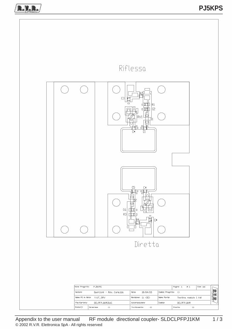
Appendix to the user manual© 2002 R.V.R. Elettronica SpA - All rights reserved
RF module directional coupler- SLDCLPFPJ1KM
PJ5KPS
1 / 3
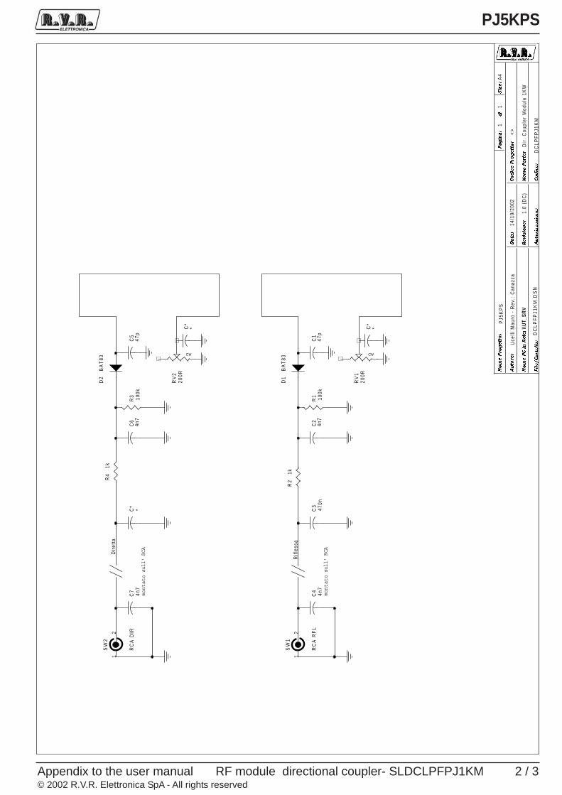
Appendix to the user manual© 2002 R.V.R. Elettronica SpA - All rights reserved
RF module directional coupler- SLDCLPFPJ1KM
PJ5KPS
2 / 3
montato sull' RCA
montato sull' RCA
\\UT_
SRV
Dir
. C
oupl
er M
odul
e 1K
W
DC
LPF
PJ1
KM
1.0
(DC
)
PJ5
KP
S
<>
DC
LPF
PJ1
KM
.DS
N
Uce
lli M
auro
- R
ev.:
Can
azza
14/1
0/20
02
11
A4
� ���
� ����
�� ��
� ��
��
� �� ��
� ����
�� ��
� ���
�� �
� �� ��
� � �� � ��
� ��� ��
� �� ��
� �� � ����
� �� ���
� ���
� ��� ��
� ��
����
����
� �� ���
� ���
�
Rif
less
a
Dir
etta
C7
4n7
C* *
C4
4n7
R3 10
0k
D2
BA
T83
C6
4n7
C5
47p
C3
470n
R1 10
0k
C*
* C*
*
C2
4n7
SW
1
RC
A R
FL
12
SW
2
RC
A D
IR
12
D1
BA
T83
R2
1k
cw
RV
220
0R
R4
1k
C1
47p
cwR
V1
200R
Appendix to the user manual© 2002 R.V.R. Elettronica SpA - All rights reserved
RF module directional coupler- SLDCLPFPJ1KM
PJ5KPS
3 / 3
SLDCLPFPJ1KM Bill Of Materials Page 1
Item Q.ty Reference Part____________________________________________________________________________________________
1 1 C* *2 2 C5,C1 47p3 4 C2,C4,C6,C7 4n74 1 C3 470n5 2 D2,D1 BAT836 2 RV2,RV1 200R7 2 R3,R1 100k8 2 R2,R4 1k9 1 SW1 RCA RFL10 1 SW2 RCA DIR

Appendix to the user manual© 2002 R.V.R. Elettronica SpA - All rights reserved
Splitter measurement board - SLSPLMEA5KW1
PJ5KPS
1 / 3
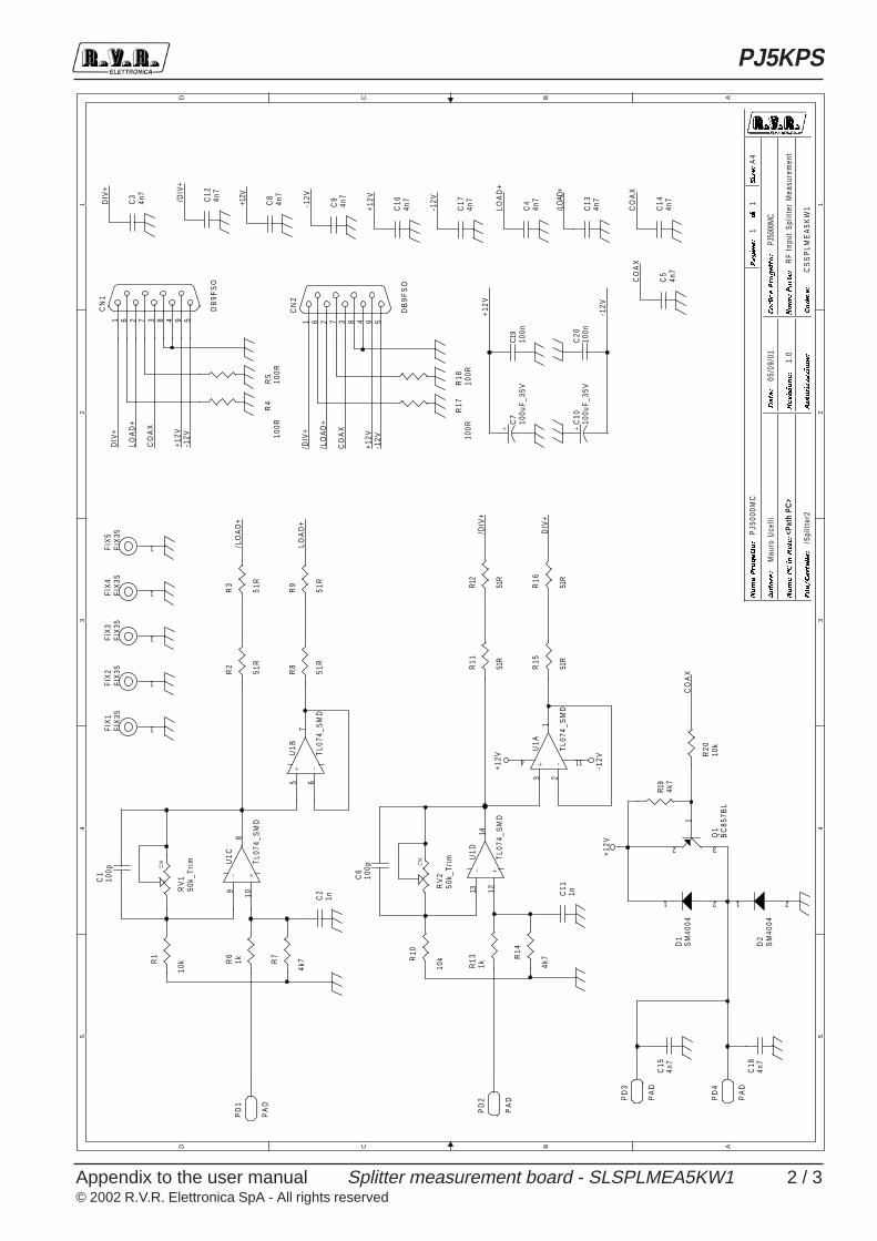
Appendix to the user manual© 2002 R.V.R. Elettronica SpA - All rights reserved
Splitter measurement board - SLSPLMEA5KW1
PJ5KPS
2 / 3
5 5
4 4
3 3
2 2
1 1
DD
CC
BB
AA
<Pat
h PC
>R
F In
put
Spl
itte
r M
easu
rem
ent
CS
SP
LME
A5K
W1
1.0
PJ5
000M
C
PJ50
00M
C
/Spl
itter
2
Mau
ro U
celli
05/0
9/01
11
A4
� ���
� ����
�� ��
� ��
��
� �� ��
� ����
�� ��
� ���
�� �
� �� ��
� � �� � ��
� ��� ��
� �� ��
� �� � ����
� �� ���
� ���
� ��� ��
� ��
����
����
� �� ���
� ���
�
DIV
+
LOA
D+
/DIV
++1
2V
DIV
+
-12V
/DIV
+
/LO
AD
+
/LO
AD+
LOA
D+
/LO
AD
+
LOA
D+
-12V
CO
AX
+12V
+12V
-12V
CO
AX
DIV
+
CO
AX
-12V
+12V
/DIV
+
+12V
-12V
CO
AX
CO
AX
+12V
-12V
+12V
R20
10k
R18
100R
C6
100p
C18
4n7
CN
2
DB
9FS
O
594837261
R13
1k
CN
1
DB
9FS
O
594837261
C20
100n
C12
4n7
R14
4k7
+-
U1
C
TL0
74_S
MD
1098
R15
51R
Q1
BC
857B
L
3
1
2
C11
1n
+ -
U1A
TL0
74_S
MD
3 21
114
C16
4n7
R16
51R
C8
4n7
R11
51R
PD
1
PA
D
PD
2
PA
D PD
3
PA
D
+C
710
0uF
_35V
PD
4
PA
D
R8
51R
+ -
U1B
TL0
74_S
MD
5 67
C1
100p
R4
100R
C15
4n7
cw
RV
150
k_T
rim
FIX
1FI
X35
1
FIX
2FI
X35
1
FIX
3FI
X35
1
FIX
4FI
X35
1
R6
1k
FIX
5FI
X35
1
R9
51R
R7
4k7
R2
51R
C19
100n
D1
SM
4004
21
+-
U1
D
TL0
74_S
MD
121314
C9
4n7
D2
SM
4004
21
cw
RV
250
k_T
rim
R3
51R
R12
51R
R19
4k7
R5
100R
R1
10k R
10
10k
C4
4n7
C13
4n7
C17
4n7
+C
1010
0uF
_35V
R17
100R
C2
1n
C3
4n7
C5
4n7
C14
4n7

Appendix to the user manual© 2002 R.V.R. Elettronica SpA - All rights reserved
Splitter measurement board - SLSPLMEA5KW1
PJ5KPS
3 / 3
CSSPLMEA5KW1 Bill Of Materials Page1
Item Q.ty Reference Part_____________________________________________________________________________________________
1 2 CN2,CN1 DB9FSO2 2 C6,C1 100p3 2 C11,C2 1n4 12 C3,C4,C5,C8,C9,C12,C13, 4n7
C14,C15,C16,C17,C185 2 C7,C10 100uF_35V6 2 C19,C20 100n7 2 D1,D2 SM40048 5 FIX1,FIX2,FIX3,FIX4,FIX5 FIX359 4 PD1,PD2,PD3,PD4 PAD10 1 Q1 BC857BL11 2 RV2,RV1 50k_Trim12 3 R1,R10,R20 10k13 8 R2,R3,R8,R9,R11,R12,R15, 51R
R1614 4 R4,R5,R17,R18 100R15 2 R13,R6 1k16 3 R7,R14,R19 4k717 1 U1 TL074_SMD
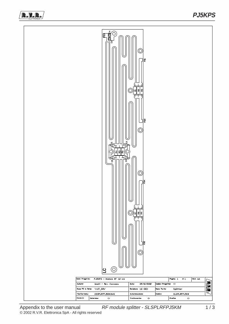
Appendix to the user manual© 2002 R.V.R. Elettronica SpA - All rights reserved
RF module splitter - SLSPLRFPJ5KM
PJ5KPS
1 / 3
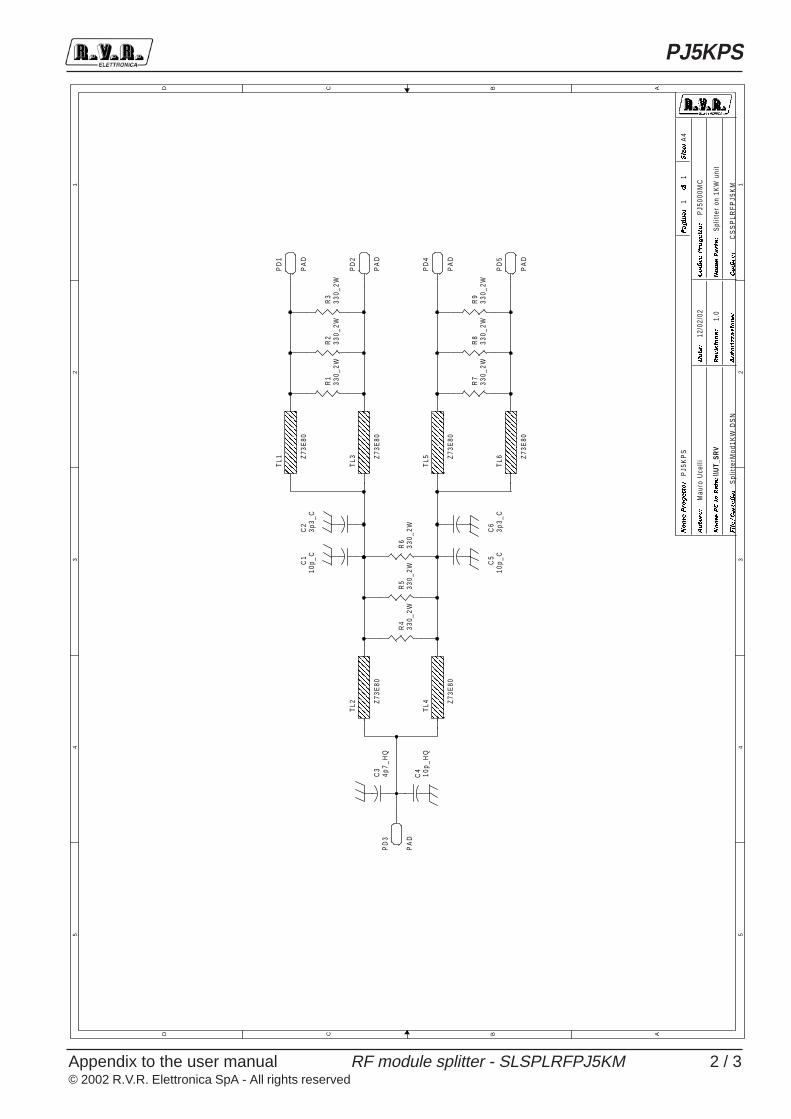
Appendix to the user manual© 2002 R.V.R. Elettronica SpA - All rights reserved
RF module splitter - SLSPLRFPJ5KM
PJ5KPS
2 / 3
5 5
4 4
3 3
2 2
1 1
DD
CC
BB
AA
\\UT_
SRV
Spl
itte
r on
1K
W u
nit
CS
SP
LRF
PJ5
KM
1.0
PJ5
KP
S
PJ5
000M
C
Spl
itte
rMod
1KW
.DS
N
Mau
ro U
celli
12/0
2/02
11
A4
� ���
� ����
�� ��
� ��
��
� �� ��
� ����
�� ��
� ���
�� �
� �� ��
� � �� � ��
� ��� ��
� �� ��
� �� � ����
� �� ���
� ���
� ��� ��
� ��
����
����
� �� ���
� ���
�
PD
2
PA
D
TL2 Z
73E
80
TL4 Z
73E
80
PD
4
PA
D
C1
10p_
C
PD
5
PA
D
PD
3
PA
D
PD
1
PA
D
R4
330_
2WC
410
p_H
Q
C3
4p7_
HQ
TL5 Z
73E
80
TL1 Z
73E
80
TL6 Z
73E
80
C5
10p_
C
TL3 Z
73E
80
R7
330_
2W
C2
3p3_
C
R1
330_
2W
R8
330_
2W
R2
330_
2W
R9
330_
2W
R3
330_
2W
C6
3p3_
C
R5
330_
2WR
633
0_2W

Appendix to the user manual© 2002 R.V.R. Elettronica SpA - All rights reserved
RF module splitter - SLSPLRFPJ5KM
PJ5KPS
3 / 3
CSSPLRFPJ5KM Bill Of Materials Page 1
Item Q.ty Reference Part____________________________________________________________________________________________
1 2 C5,C1 10p_C2 2 C6,C2 3p3_C3 1 C3 4p7_HQ4 1 C4 10p_HQ5 5 PD1,PD2,PD3,PD4,PD5 PAD6 9 R1,R2,R3,R4,R5,R6,R7,R8, 330_2W
R97 6 TL1,TL2,TL3,TL4,TL5,TL6 Z73E80
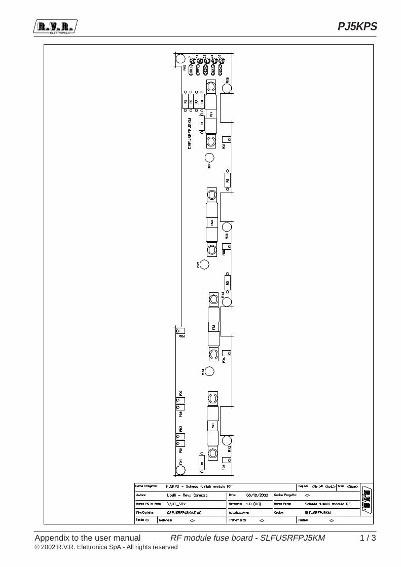
Appendix to the user manual© 2002 R.V.R. Elettronica SpA - All rights reserved
RF module fuse board - SLFUSRFPJ5KM
PJ5KPS
1 / 3
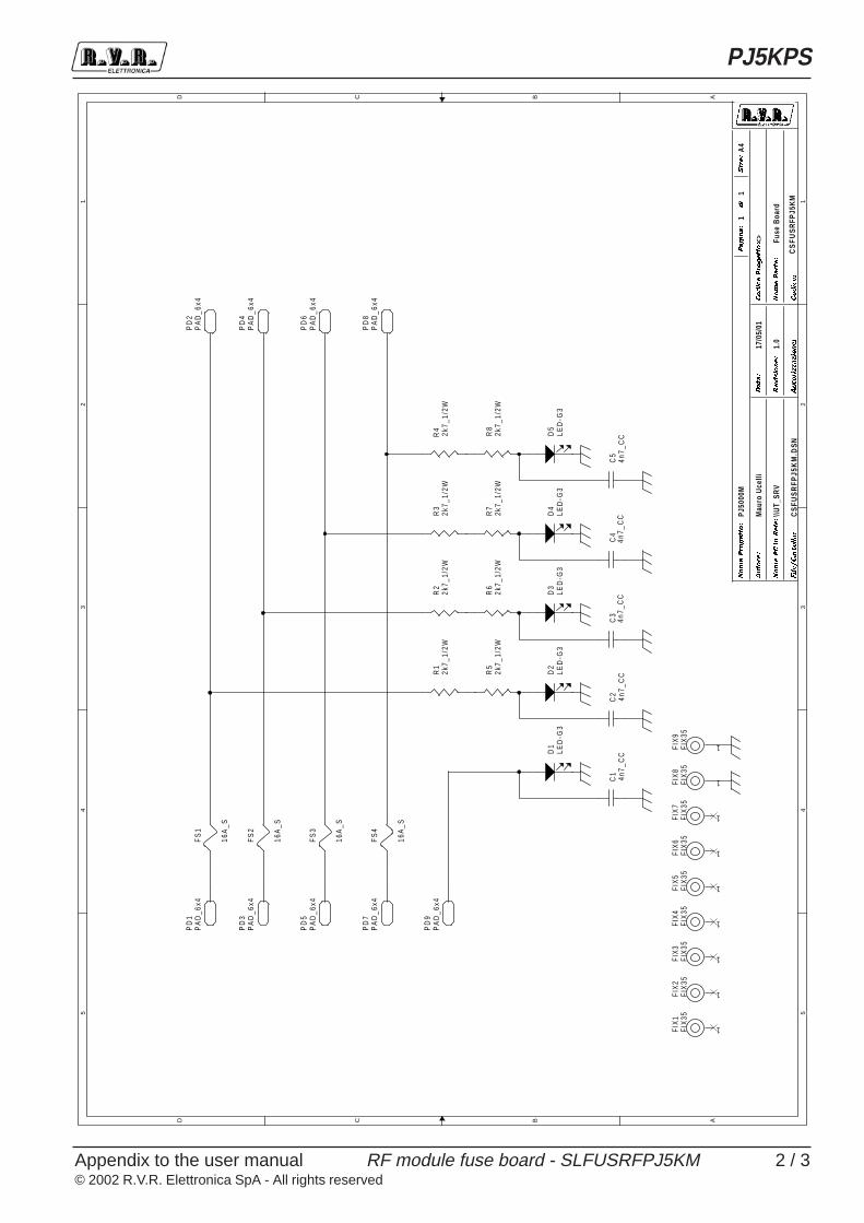
Appendix to the user manual© 2002 R.V.R. Elettronica SpA - All rights reserved
RF module fuse board - SLFUSRFPJ5KM
PJ5KPS
2 / 3
5 5
4 4
3 3
2 2
1 1
DD
CC
BB
AA
PJ50
00M
<>
1
Mau
ro U
celli
Fuse
Boa
rd
CS
FUSR
FPJ5
KM
\\UT_
SRV
CS
FUS
RFP
J5K
M.D
SN
17/0
5/01
A4
1
1.0
� ���
� ������ ��
� � ��
� ��� ��� ��
���� ��
� ���
� ! "# �$ �%
&'( )* + ,-. )(( ,/
0 12 13 4 567 87 9:5;
< 9=7 >5;
? 9@5
A BCD 5;
E FG HIJ KKLKJ HMNO
P LQJ MLO
RS TUV
WSP
D1
PA
D_6
x4
PD
3P
AD
_6x4
PD
5P
AD
_6x4
PD
7P
AD
_6x4
PD
9P
AD
_6x4
PD
2P
AD
_6x4
FIX
1FI
X35
1
PD
4P
AD
_6x4
FIX
2FI
X35
1
PD
6P
AD
_6x4
FIX
3FI
X35
1
PD
8P
AD
_6x4
FIX
4FI
X35
1
FIX
5FI
X35
1
D1
LED
-G3
FIX
6FI
X35
1
D2
LED
-G3
FIX
7FI
X35
1
D3
LED
-G3
FIX
8FI
X35
1
D4
LED
-G3
FIX
9FI
X35
1
D5
LED
-G3
FS
1
16A
_S
FS
2
16A
_S
FS
3
16A
_S
R5
2k7_
1/2W
FS
4
16A
_S
R1
2k7_
1/2W
R6
2k7_
1/2W
R2
2k7_
1/2W
R7
2k7_
1/2W
R3
2k7_
1/2W
R8
2k7_
1/2W
R4
2k7_
1/2W
C1
4n7_
CC
C2
4n7_
CC
C3
4n7_
CC
C4
4n7_
CC
C5
4n7_
CC
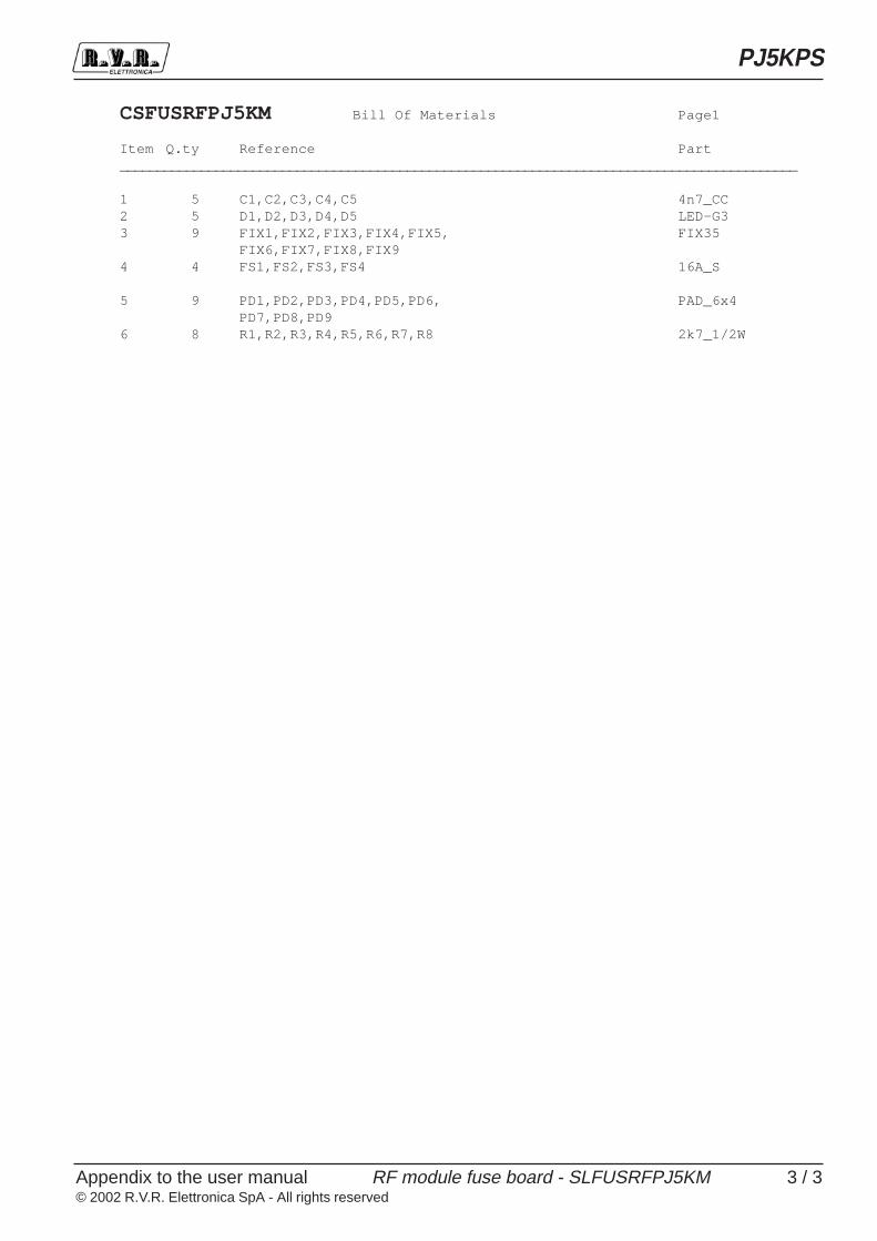
Appendix to the user manual© 2002 R.V.R. Elettronica SpA - All rights reserved
RF module fuse board - SLFUSRFPJ5KM
PJ5KPS
3 / 3
CSFUSRFPJ5KM Bill Of Materials Page1
Item Q.ty Reference Part____________________________________________________________________________________________
1 5 C1,C2,C3,C4,C5 4n7_CC2 5 D1,D2,D3,D4,D5 LED-G33 9 FIX1,FIX2,FIX3,FIX4,FIX5, FIX35
FIX6,FIX7,FIX8,FIX94 4 FS1,FS2,FS3,FS4 16A_S
5 9 PD1,PD2,PD3,PD4,PD5,PD6, PAD_6x4PD7,PD8,PD9
6 8 R1,R2,R3,R4,R5,R6,R7,R8 2k7_1/2W
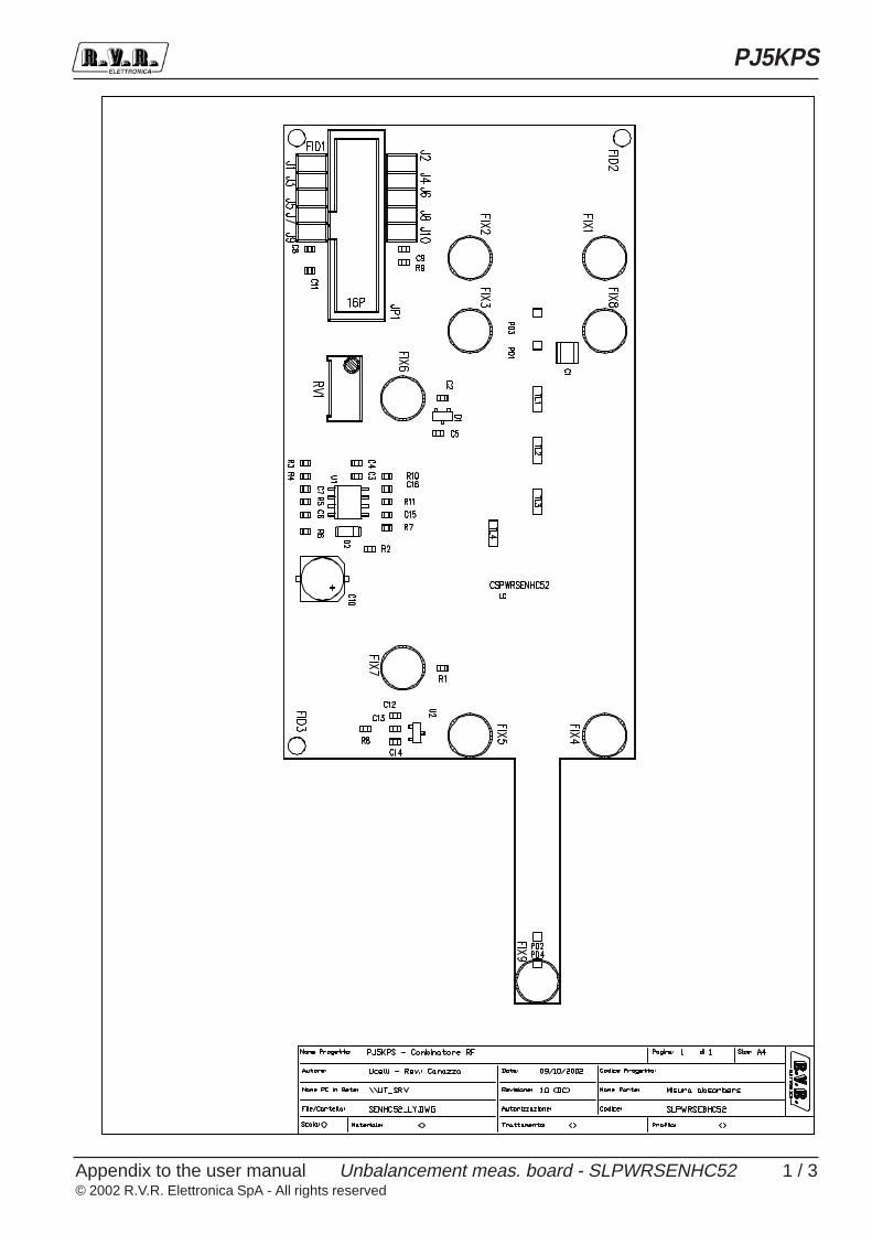
Appendix to the user manual© 2002 R.V.R. Elettronica SpA - All rights reserved
Unbalancement meas. board - SLPWRSENHC52
PJ5KPS
1 / 3
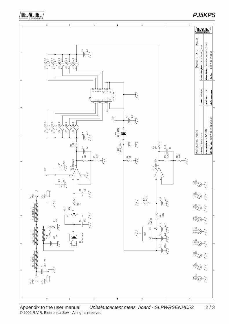
Appendix to the user manual© 2002 R.V.R. Elettronica SpA - All rights reserved
Unbalancement meas. board - SLPWRSENHC52
PJ5KPS
2 / 3
5 5
4 4
3 3
2 2
1 1
DD
CC
BB
AA
\\UT_
SRV
Abs
orbe
r M
easu
re C
ircu
it
CS
PW
RS
EN
HC
52
1.0
PJ5
KP
S
PJ5
000M
C_C
ode
CS
PW
RS
EN
HC
52
.DS
N
Mau
ro U
celli
23/0
1/02
11
A4
� ���
� ����
�� ��
� ��
��
� �� ��
� ����
�� ��
� ���
�� �
� �� ��
� � �� � ��
� ��� ��
� �� ��
� �� � ����
� �� ���
� ���
� ��� ��
� ��
����
����
� �� ���
� ���
�
+12V
+12V
J6JS
MD 1
2
J7JS
MD 1
2
C5
4n7
TL1
TLI
NE
_L
C7
1n
J8JS
MD 1
2
J9JS
MD 1
2
RV
1
50k
3
2
1
C16
1n
J10
JSM
D 12
C2
33p
FIX
4FI
X35
C1
2p2_
HQ
1 2
PD
3P
AD
U2
LM50
C
1
3
2
VS
GN
D
V0
D2
5V1_
SM
D
21
C13
4n7
C14
4n7
C12
100n
FIX
1FI
X35
R8
10k0
FIX
5FI
X35
FIX
7FI
X35
C15
4n7
FIX
2FI
X35
R6
1k
C4
100n
+ -
U1A
LM35
8SM
D3 2
1
48
+ -
U1B
LM35
8SM
D5 6
7
+
C10
100u
F_3
5V
R3
100
FIX
6FI
X35
R4
10k
R7
64k9
C3
4n7
TL2
TLI
NE
_L
TL4
TLI
NE
_M
PD
1P
AD
FIX
3FI
X35
PD
2P
AD
R2
1k
JP1
FLA
T16
V
12
34
56
78
910
1112
1314
1516
R5
2.2k
FIX
8FI
X35
PD
4P
AD
J1JS
MD 1
2
TL3
TLI
NE
_L
R10
10k0
J2JS
MD 1
2
FIX
9FI
X35
R1
100
J3JS
MD 1
2
C11
4n7
D1
HS
MS
2800
1 23
R11
4k99
C6
1nC
8
4n7
J4JS
MD 1
2
J5JS
MD 1
2
R9
100
C9
4n7
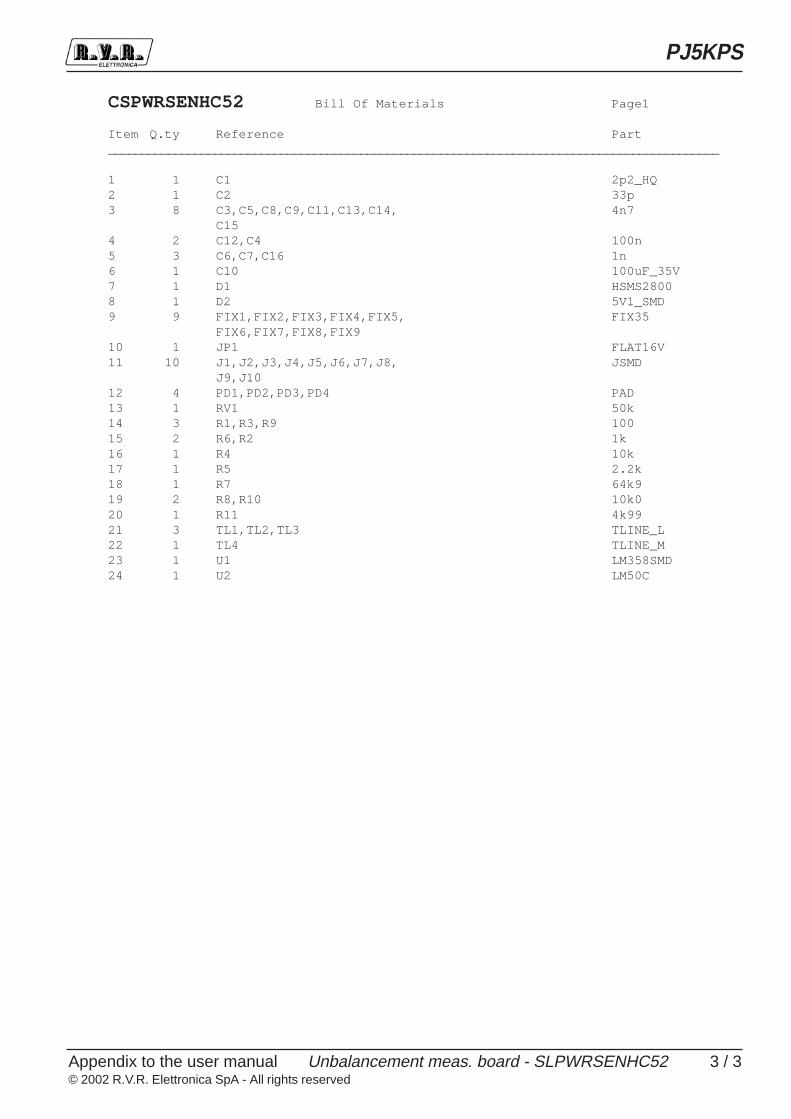
Appendix to the user manual© 2002 R.V.R. Elettronica SpA - All rights reserved
Unbalancement meas. board - SLPWRSENHC52
PJ5KPS
3 / 3
CSPWRSENHC52 Bill Of Materials Page1
Item Q.ty Reference Part____________________________________________________________________________________________
1 1 C1 2p2_HQ2 1 C2 33p3 8 C3,C5,C8,C9,C11,C13,C14, 4n7
C154 2 C12,C4 100n5 3 C6,C7,C16 1n6 1 C10 100uF_35V7 1 D1 HSMS28008 1 D2 5V1_SMD9 9 FIX1,FIX2,FIX3,FIX4,FIX5, FIX35
FIX6,FIX7,FIX8,FIX910 1 JP1 FLAT16V11 10 J1,J2,J3,J4,J5,J6,J7,J8, JSMD
J9,J1012 4 PD1,PD2,PD3,PD4 PAD13 1 RV1 50k14 3 R1,R3,R9 10015 2 R6,R2 1k16 1 R4 10k17 1 R5 2.2k18 1 R7 64k919 2 R8,R10 10k020 1 R11 4k9921 3 TL1,TL2,TL3 TLINE_L22 1 TL4 TLINE_M23 1 U1 LM358SMD24 1 U2 LM50C
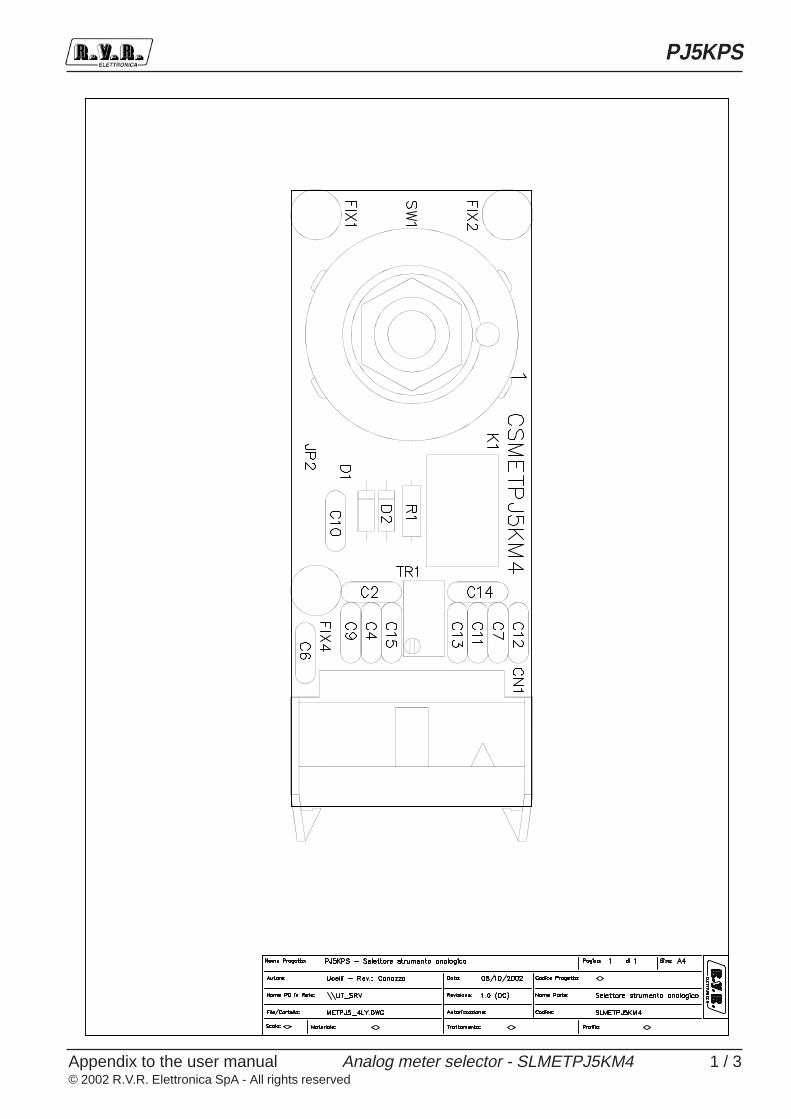
Appendix to the user manual© 2002 R.V.R. Elettronica SpA - All rights reserved
Analog meter selector - SLMETPJ5KM4
PJ5KPS
1 / 3
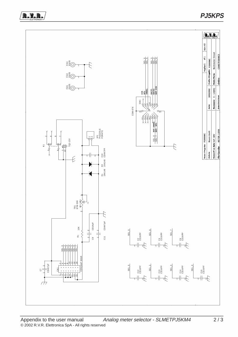
Appendix to the user manual© 2002 R.V.R. Elettronica SpA - All rights reserved
Analog meter selector - SLMETPJ5KM4
PJ5KPS
2 / 3
5 5
4 4
3 3
2 2
1 1
DD
CC
BB
AA
DIR
RFL
EXCT1
EXCT2
UNBAL
EXT.DIR
EXT. RFL
EXT UNBAL
PJ50
00M
C
PJ50
00M
C
1
Mau
ro U
celli
Mul
tim
eter
Cir
cuit
CS
ME
TPJ5
KM
C3
\\UT_
SRV
ME
TER
_3.D
SN
18/0
2/20
02
A3
1
C -
1.0
(DC
)
� ���
� ������ �
�� ���
� ��� ��� ��
���� ��
� ���
!" #$ %& %'
()* +, - ./0 +** .1
2 34 35 6 789 :9 ;<7=
> ;?9 @7=
A ;B7
C DEF 7=
G HI JKL MMNML JOPQ
R NSL ONQ
TU VWX
YU
SE
L_2
SE
L_3
SE
L_7
SE
L_4
SE
L_0
SE
L_5
SE
L_6
SE
L_0
SE
L_3
SE
L_2
SE
L_5
SE
L_4
SE
L_7
SE
L_6
SE
L_5
SE
L_6
SE
L_7
SE
L_0
SE
L_2
SE
L_3
SE
L_4
JP2
PIA
ZZ
OLE
FO
RA
TE
1 2
SW
1
CO
M-6
76
13
2 3 64 589
1
101112 7
14
15
16
C13
CD
1K
PF
1 2
C7
CD
4K7p
F
12
D2
1N41
48
FIX
1F
IX35
1
C14
CD
1K
PF
1 2
C10
CD
4K7P
F
1 2
C11
CD
4K7p
F
12
FIX
2F
IX35
1
C15
CD
1K
PF
1 2
C9
CD
1KpF
12
R1
10K
C12
CD
1K
PF
1 2
C4
CD
1K
PF
1 2
TR
18
7W
-50
K
13
2
FIX
4F
IX35
1
CN
1
CO
N16
AP
90G
R
1 3 5 7 9 11 13 15
2 4 6 8 10 12 14 16
+ + + + + + + +
+ + + + + + + +
C2
CD
1K
PF
1 2
C6
CD
1K
PF
1 2
D1
1N41
48
+
K1
TQ
2-12
V
32 4
89 7
1 10

Appendix to the user manual© 2002 R.V.R. Elettronica SpA - All rights reserved
Analog meter selector - SLMETPJ5KM4
PJ5KPS
3 / 3
SLMETPJ5KM4 Bill Of Materials Page 1
Item Q.ty Reference Part____________________________________________________________________________________________
1 1 CN1 CON16AP 90GR2 8 C2,C4,C6,C9,C12,C13,C14,
C15 CD1KpF3 3 C7,C10,C11 CD4K7pF4 2 D1,D2 1N41485 3 FIX1,FIX2,FIX4 FIX356 1 JP2 PIAZZOLE7 1 K1 TQ2-12V8 1 R1 10K9 1 SW1 COM-67610 1 TR1 87W-50K
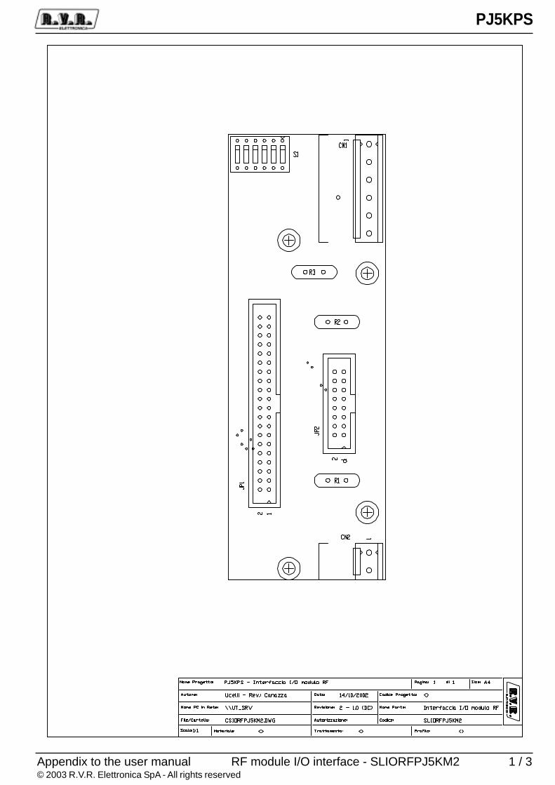
Appendix to the user manual© 2003 R.V.R. Elettronica SpA - All rights reserved
RF module I/O interface - SLIORFPJ5KM2
PJ5KPS
1 / 3

Appendix to the user manual© 2003 R.V.R. Elettronica SpA - All rights reserved
RF module I/O interface - SLIORFPJ5KM2
PJ5KPS
2 / 3
55
44
33
22
11
DD
CC
BB
AA
BUS CU
18V_UP
18V_DW
62VAC
IN_SWSAFE
MICROSWITCH
MODULE INSERTED
<Path P
C>
Interface I/O 1K
W U
nit
CS
IOR
FP
J5KM
2
1.2
PJ5000M
C
PJ5000M
C_C
ode
/Address_1.dsn
Mauro U
celli15/12/03
11
A4
���
���
�����
���
��
�������
�����
���
���
���
����
����
� ���
���
���
�������
��
�����
���
���
���
���
����������
�����
�
����
��
IN_A
D2
IN_A
D3
IN_A
D5
IN_A
D0
IN_A
D1
IN_A
D4
OC
_ALA
RM
IN_S
TD
BY
IN_O
N TR
-T
R+
IN_S
TD
BY
IN_O
N
OC
_ALA
RM
IN_G
FB
TR
-
IN_A
D0
IN_A
D1
IN_A
D2
IN_A
D3
IN_A
D4
IN_A
D5
IN_G
FB
_RIN
_GF
B
IN_G
FB
_RT
R+
JP2
HE
AD
ER
8X2
12
34
56
78
910
1112
1314
1516
CN
2
PH
OE
NIX
2
12
R2
RX
E110
JP1
HE
AD
ER
20X2
12
34
56
78
910
1112
1314
1516
1718
1920
2122
2324
2526
2728
2930
3132
3334
3536
3738
3940
R1
RX
E110
CN
1
PH
OE
NIX
6
123456
FIX
1F
IX35
FIX
2F
IX35
FIX
3F
IX35
FIX
4F
IX35
R3
PT
C_1
S1
SW
DIP
-6
123456
121110987
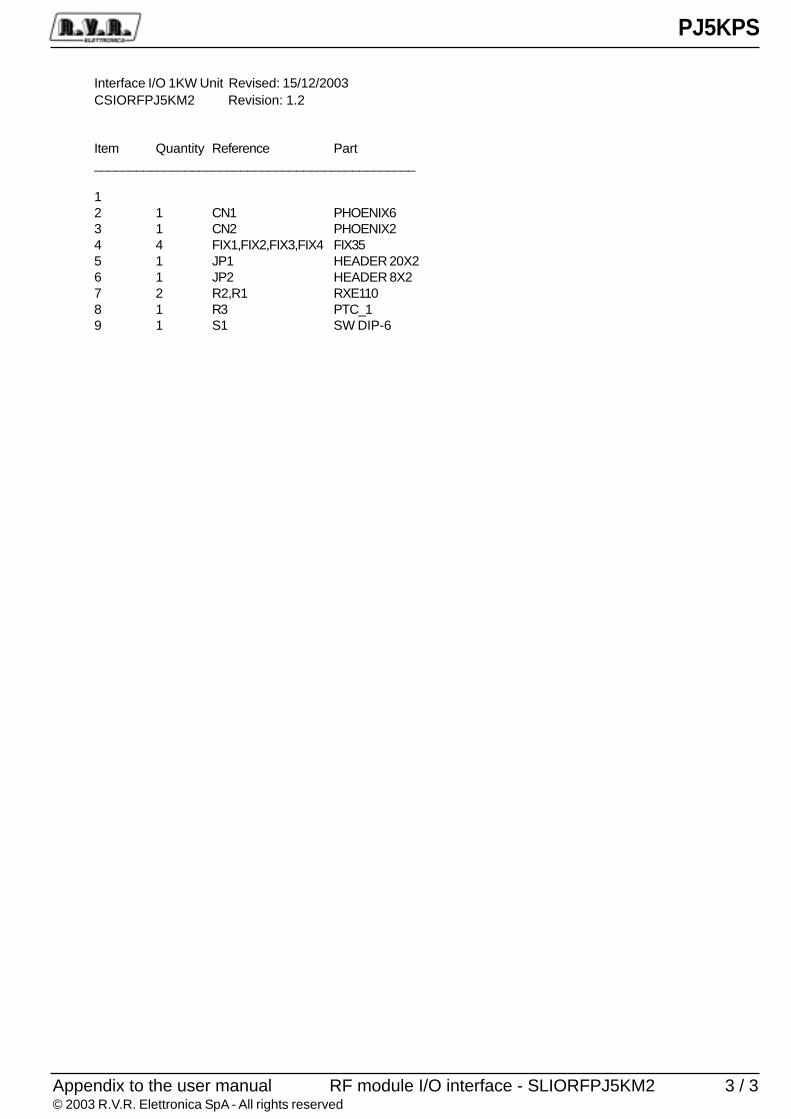
Appendix to the user manual© 2003 R.V.R. Elettronica SpA - All rights reserved
RF module I/O interface - SLIORFPJ5KM2
PJ5KPS
3 / 3
Interface I/O 1KW Unit Revised: 15/12/2003CSIORFPJ5KM2 Revision: 1.2
Item Quantity Reference Part______________________________________________
12 1 CN1 PHOENIX63 1 CN2 PHOENIX24 4 FIX1,FIX2,FIX3,FIX4 FIX355 1 JP1 HEADER 20X26 1 JP2 HEADER 8X27 2 R2,R1 RXE1108 1 R3 PTC_19 1 S1 SW DIP-6
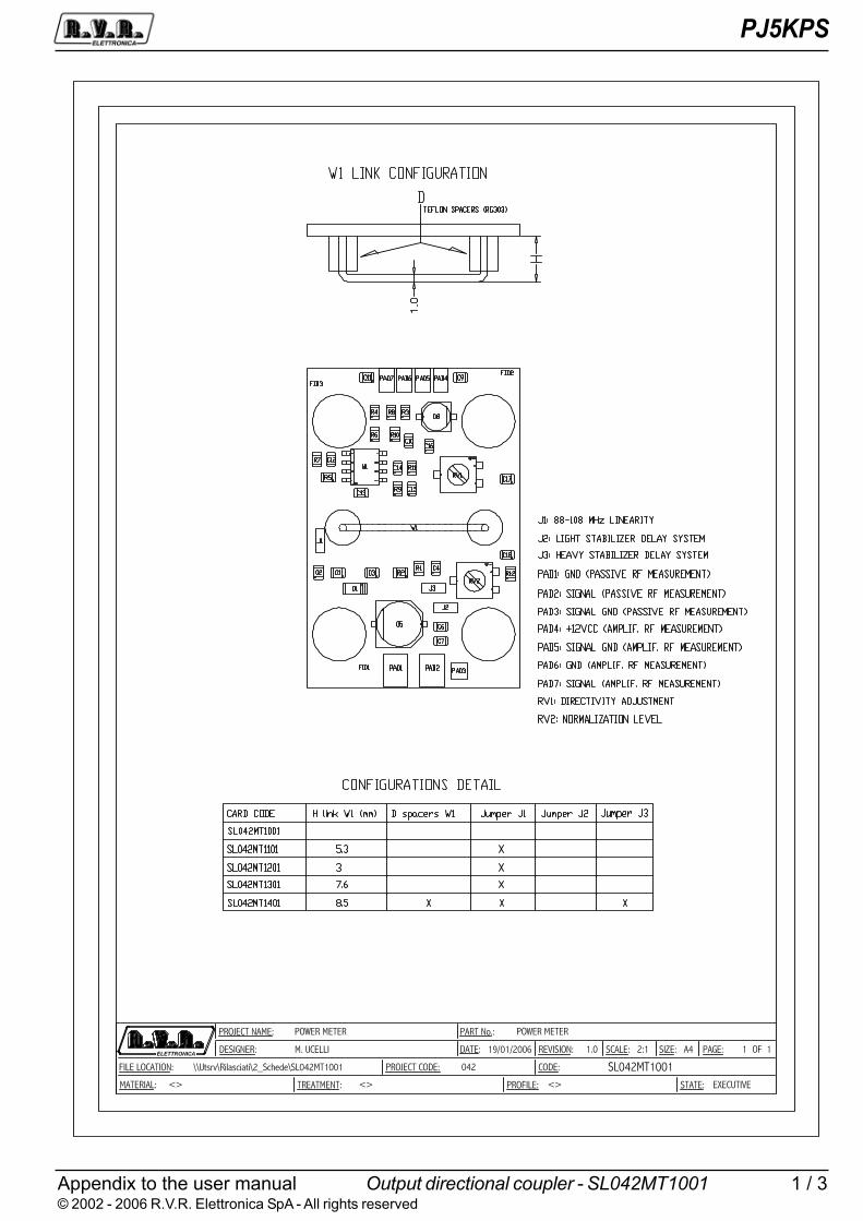
Appendix to the user manual© 2002 - 2006 R.V.R. Elettronica SpA - All rights reserved
Output directional coupler - SL042MT1001
PJ5KPS
1 / 3
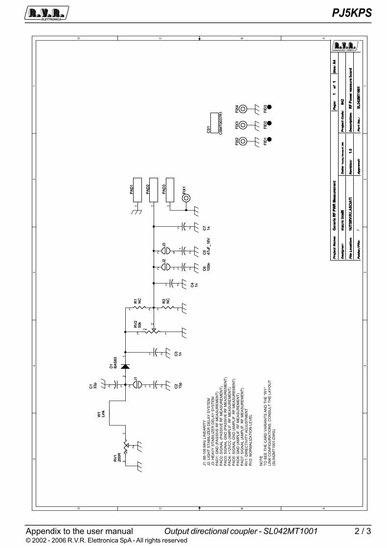
Appendix to the user manual© 2002 - 2006 R.V.R. Elettronica SpA - All rights reserved
Output directional coupler - SL042MT1001
PJ5KPS
2 / 3
� �
� �
� �
� �
� �
��
��
�����
��
��
�
�����
���
�����
������
�����
�������
����
�������
����
�����
���
����
��
�������
����
��������
����
���
�
�
���������������
�� ����� ������� �����
����������
���
�� ��!" �� �#� ��������� $
���
����� �"�%%!
��
�
������&' �������& �(' ���)
*
�����
��
��
�
�����
���
�����
������
�����
�������
����
�������
����
�����
���
����
��
�������
����
��������
����
���
�
�
���������������
�� ����� ������� �����
����������
���
�� ��!" �� �#� ��������� $
���
����� �"�%%!
��
�
������&' �������& �(' ���)
*
�����
��
��
�
�����
���
�����
������
�����
�������
����
�������
����
�����
���
����
��
�������
����
��������
����
���
�
�
���������������
�� ����� ������� �����
����������
���
�� ��!" �� �#� ��������� $
���
����� �"�%%!
��
�
������&' �������& �(' ���)
*
��� ����
�� �
�� �
���
�
���
��� ���
�� �
�
��
���
� �
��
� �
��
��
���� �
�
��
��
��
���
� �
��
� �
��
��
��
�
�� �
��
�
�
���
� �
! �
�
�"
��
��
��#
�
��� �
���
� �
�
���
� �
! �
�
�"
��
��
��#
�
��� �
���
� �
��
�
�
���
� �
! �
�
�"
��
��
��#
�
��� $���
��
��
��!
% �
! �
�
�"
��
��
��#
�
��� �
���
� �
��
��
��!
% �
! �
�
�"
��
��
��#
�
�&� �
��
��
��!
% �
! �
�
�"
��
��
��#
�
�'� �
���
�
��
��!
% �
! �
�
�"
��
��
��#
��
�� �
���
����
���
�
�"
���
��
��
��� �
(�
�
���
��(
� �
��
��
�(
��
�(
��
� �
��
�
��
�
��
���
�
� �
��
)*
�)
���
+ �
(�
!��
"�
��(
��
, �
(�
�"
�� �
��
�
�(
"�
������
�������
*�
#
!�-
�!�-
�
� �
��
��.
��
��.
� �
��
�/
��
�/
!��
�!��
�
� �
��
��
��
��
!��
�!��
�
��
�
��
��
�����
��
��
�����
��
��
��.
��
��.
��
�
��
��
���0
��
��
���0
!��
�!��
�
��
�
��
�����'�
�
��
�
��
�����'�
�
��
��
��
� �
�'
�/
�'
�/
!�-
�!�-
�� �
��
��
��
��
� �
�&
���/
�&
���/
�
�
��
�
��
*�
�1/
0*
��1/
0
��
��
��
!�-
�!�-
�
�
�
��
�
��
��
��
���
�
��
���
��
���
�
�
��
�
��
� �
��
�/
��
�/
� ��
��
�'2!3�&�
�
��
�'2!3�&�
!�-
�!�-
�
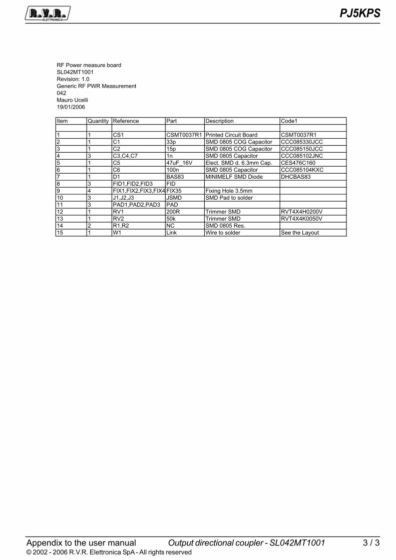
Appendix to the user manual© 2002 - 2006 R.V.R. Elettronica SpA - All rights reserved
Output directional coupler - SL042MT1001
PJ5KPS
3 / 3
�! �4567 869:276 ;497<
�����������
�6=1:14/� �%�
�6/671> �! �*� �69:27686/?
���
�9274 ">6@@1
�AB��B���&
�?68 C29/?1?D �6E676/>6 �97? �6:>71.?14/ �4<6�
� � ��� �������'�� �71/?6< �17>21? 497< �������'��
� � �� ��. ��� ���� �(� �9.9>1?47 ������������
� � �� ��. ��� ���� �(� �9.9>1?47 ������������
� � ��,��,�' �/ ��� ���� �9.9>1?47 ������������
� � �� �'2!3�&� �@6>?% ��� <% &%�88 �9.% ����'&��&�
& � �& ���/ ��� ���� �9.9>1?47 ���������+-�
' � �� ��� �������! ��� �14<6 ������
� � !���,!���,!��� !��
A � !�-�,!�-�,!�-�,!�-� !�-�� !1F1/G �4@6 �%�88
�� � ��,��,�� ���� ��� �9< ?4 :4@<67
�� � ���,���,��� ��
�� � ��� ���� �718867 ��� ����-�������
�� � ��� ��0 �718867 ��� ����-�+�����
�� � ��,�� �� ��� ���� �6:%
�� � *� �1/0 *176 ?4 :4@<67 �66 ?H6 �9D42?
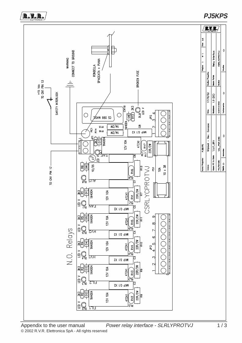
Appendix to the user manual© 2002 R.V.R. Elettronica SpA - All rights reserved
Power relay interface - SLRLYPROTVJ
PJ5KPS
1 / 3
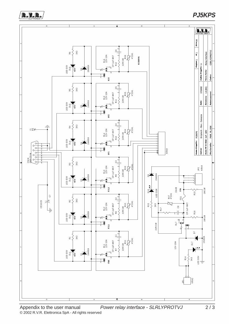
Appendix to the user manual© 2002 R.V.R. Elettronica SpA - All rights reserved
Power relay interface - SLRLYPROTVJ
PJ5KPS
2 / 3
8 8
7 7
6 6
5 5
4 4
3 3
2 2
1 1
DD
CC
BB
AA
FA
NF
IL1
FIL
2H
V1
HV
2R
IS
RIS
ER
VA
10A
PJ5K
PS
<>
1
Gri
ptec
h -
Rev
.: C
anaz
za
Rel
a y In
terf
ace
CS
RLY
CP
RO
TVJ
\\UT_
SRV
PW
R_R
L.D
SN
17/1
0/02
A41
1.0
(DC
)
1RPH3URJHWWR�
$XWRUH�
&RGLFH3URJHWWR�
1RPH3&LQ
5HWH�
)LOH�&DUWHOOD�
'DWD�
5HYLVLRQH�
&RGLFH�
1RPH3DUWH�
$XWRUL]]D]LRQH�
3DJLQD�
6L]H�
GL
FS
1
10x3
8
JP3
KR
A9
RL1
12V
-10A
43
5
21
C1
CP
.1uF
-MK
T 12
R7
22
R/1
W RV
1
47Z
A1
R8
22
R/1
W RV
2
47Z
A1
RL2
12V
-10A
43
5
21
C2
CP
.1uF
-MK
T 12
R9
22
R/1
W RV
3
47Z
A1
RL3
12V
-10A
43
5
21
C3
CP
.1uF
-MK
T 12
R10
22
R/1
W RV
4
47Z
A1
RL4
12V
-10A
43
5
21
C4
CP
.1uF
-MK
T 12
R11
22
R/1
W RV
5
47Z
A1
RL5
12V
-10A
43
5
21
C5
CP
.1uF
-MK
T 12
R12
22
R/1
W RV
6
47Z
A1
RL6
12V
-10A
43
5
21
C6
CP
.1uF
-MK
T 12
CN
18D
B9-
CS
-M
594837261
+
C7
CE
10/2
5
D1
1N40
04
DL1
LED
-D3V
R1
3K3
D2
1N40
04
R2
3K3
DL2
LED
-D3V
D3
1N40
04
R3
3K3
DL3
LED
-D3V
D4
1N40
04
R4
3K3
DL4
LED
-D3V
D5
1N40
04
R5
3K3
DL5
LED
-D3V
D6
1N40
04
R6
3K3
DL6
LED
-D3V
RL7
12V
-10A
43 5
21JP
1
KR
A2
D7
1N40
04
R14
3K3
DL7
LED
D3V
JP2
KR
A4
R13
3K3
DL8
LED
D3R
D8
1N40
04
R16
1M/1
W
R15 1M
/1W
R17
22
R/1
W
C8
CP
.1uF
-MK
T
1 2
RV
747
ZA
1
J1 PE

Appendix to the user manual© 2002 R.V.R. Elettronica SpA - All rights reserved
Power relay interface - SLRLYPROTVJ
PJ5KPS
3 / 3
SLRLYCPROTVJ Bill Of Materials Page1
Item Q.ty Reference Part____________________________________________________________________________________________1 1 CN18 DB9-CS-M2 7 C1, C2, C3, C4, C5, C6, C7 CE10/254 7 DL1, DL2, DL3, DL4, DL5, DL6, DL7 LED D3V5 1 DL8 LED D3R7 8 D1, D2, D3, D4, D5, D6, D7, D8 1N40048 1 FS1 10x389 1 JP1 KRA210 1 JP2 KRA4
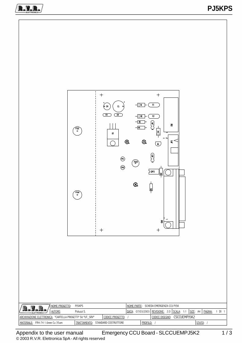
Appendix to the user manual© 2003 R.V.R. Elettronica SpA - All rights reserved
Emergency CCU Board - SLCCUEMPJ5K2
PJ5KPS
1 / 3
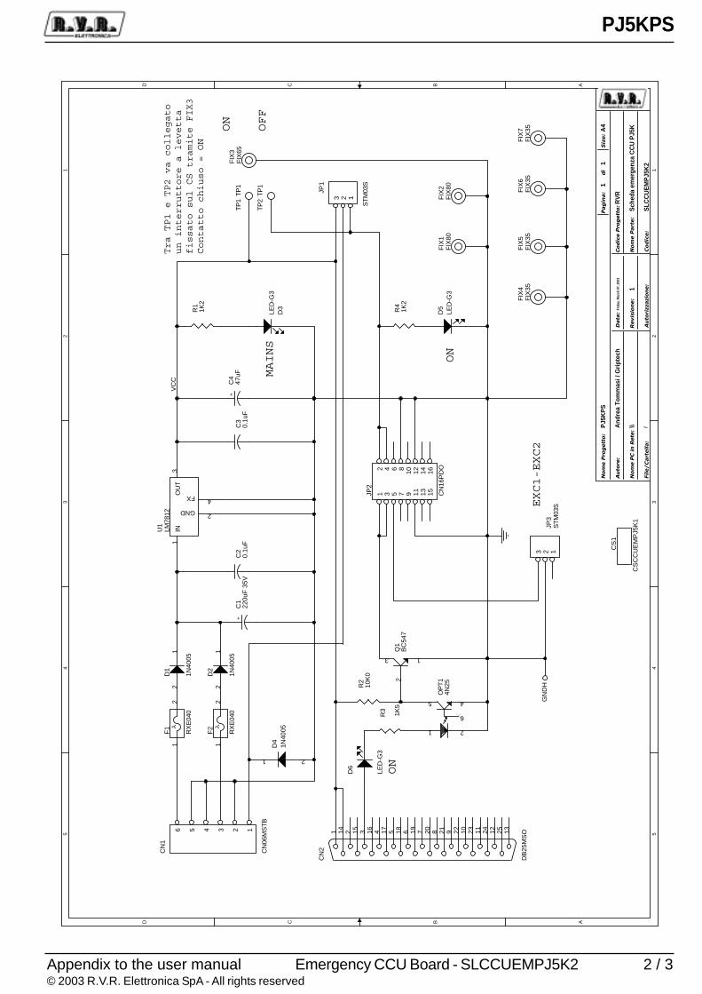
Appendix to the user manual© 2003 R.V.R. Elettronica SpA - All rights reserved
Emergency CCU Board - SLCCUEMPJ5K2
PJ5KPS
2 / 3
5 5
4 4
3 3
2 2
1 1
DD
CC
BB
AA
MAINS
ON
ON
OFF
Tra TP1 e TP2 va collegato
un interruttore a levetta
fissato sul CS tramite FIX3
Contatto chiuso = ON
EXC1-EXC2
ON
\\S
ched
a em
erge
nza
CC
U P
J5K
SLC
CU
EM
PJ5
K2
1
PJ5
KP
S
RV
RA
ndre
a To
mm
asi /
Gri
ptec
h
11
A4
Frid
ay, M
arch
07,
200
3
/
���
���
�����
���
��
�������
�����
���
���
�����
��
����� ���
���
���
�������
��
�����
���
���
���
���
����������
�����
�
����
��
VC
C
GN
DH
JP2
CN
16P
DO
12
34
56
78
910
1112
1314
1516
R2
10K
0
C2
0.1u
F
JP1
ST
M03
S
123
R4
1K2
D4
1N40
05
21
FIX
6F
IX35
D1
1N40
05
21
+C
447
uF
FIX
1F
IX80
FIX
2F
IX80
TP
1T
P1
CN
1
CN
06M
ST
B
123456
FIX
7F
IX35
CN
2
DB
25M
SO13251224112310229218207196185174163152141
JP3
ST
M03
S123
D2
1N40
05
21
TP
2T
P1
R1
1K2
U1
LM78
121
2
4
3IN
GND
FXOU
T
Q1
BC
547
2
13
D5
LED
-G3
FIX
3F
IX65
AF
1
RX
E04
0
12
R3
1K5
D6
LED
-G3
OP
T1
4N25
1 2
5 4
6
+C
122
0uF
35V
FIX
4F
IX35
D3
LED
-G3
AF
2
RX
E04
0
12
C3
0.1u
F
FIX
5F
IX35
CS
1
CS
CC
UE
MP
J5K
1
Appendix to the user manual© 2003 R.V.R. Elettronica SpA - All rights reserved
Emergency CCU Board - SLCCUEMPJ5K2
PJ5KPS
3 / 3
SLCCUEMPJ5K1 Revision: 1
Andrea Tommasi / Griptech
Item Quantity Reference Part Description_______________________________________________________________________
1 1 CN1 CN06MSTB Conn. Phoenix MSTB a 6 poli2 1 CN2 DB25MSO Connettore DB25 mas. cs 90°3 1 CS1 CSCCUEMPJ5K1 Circuito stampato4 1 C1 220uF 35V Cond. Elettr. Dia 10 P5.085 2 C2,C3 0.1uF Cond. ceramico p 5mm6 1 C4 47uF Cond. Elettr. Dia 6.5 P2.547 3 D1,D2,D4 1N4005 Diodo plastico DO418 3 D3,D5,D6 LED-G3 LED verde dia. 3mm Nota 19 2 FIX1,FIX2 FIX80 Foro fissaggio 8mm10 1 FIX3 FIX65 Foro fissaggio 6.5mm11 4 FIX4,FIX5,FIX6,FIX7 FIX35 Foro fissaggio 3.5mm12 2 F1,F2 RXE040 Fusibile autorip. 7mm13 2 JP1,JP3 STM03S Strip maschio 3 pin14 1 JP2 CN16PDO Connettore 16 poli Flat cs a 90°15 1 OPT1 4N25 Optoisolatore DIP616 1 Q1 BC547 Trans. NPN TO9217 2 R4,R1 1K2 Res. 1/4W18 1 R2 10K0 Res. 1/4W19 1 R3 1K5 Res. 1/4W20 2 TP1,TP2 NC Test point21 1 U1 LM7812 Stabilizzatore TO220
22 1 SW1 SW1V2P Deviatore fissato nel foro e collegatotra TP1 e TP2 chiuso in pos. ONCon blocco della levettaE la levetta lato saldature
Nota 1 I led vanno montati lato saldature a livello del CS
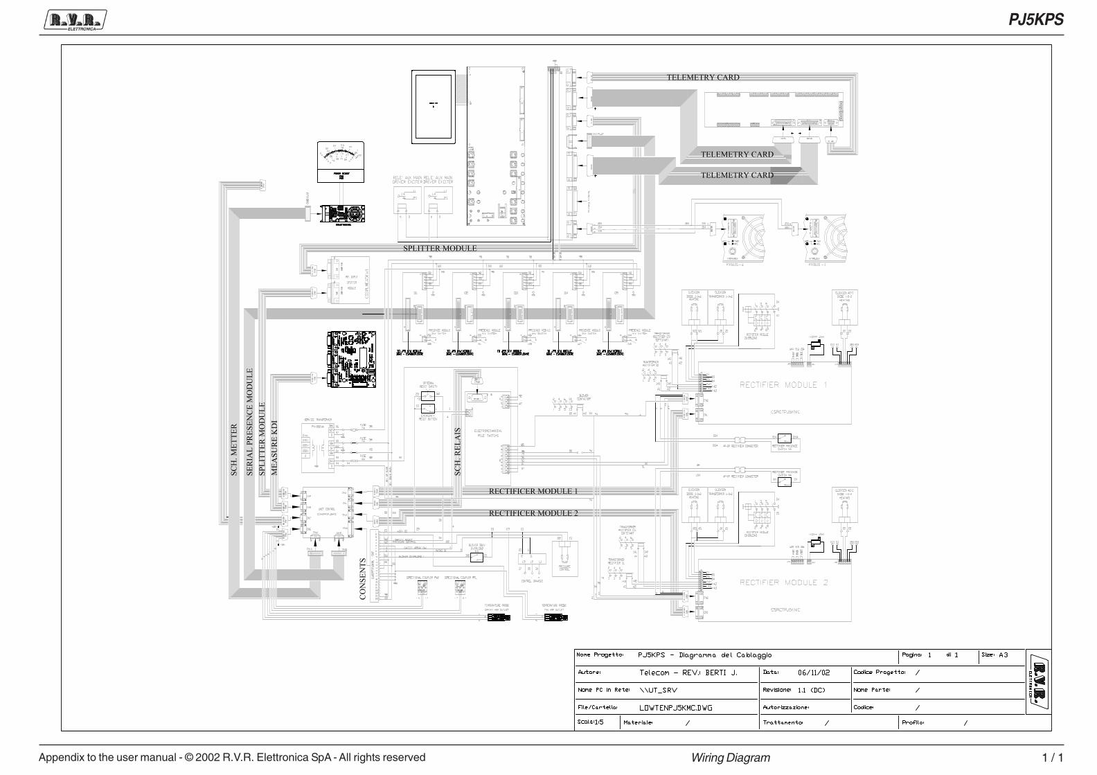
Appendix to the user manual - © 2002 R.V.R. Elettronica SpA - All rights reserved
PJ5KPS
1 / 1Wiring Diagram
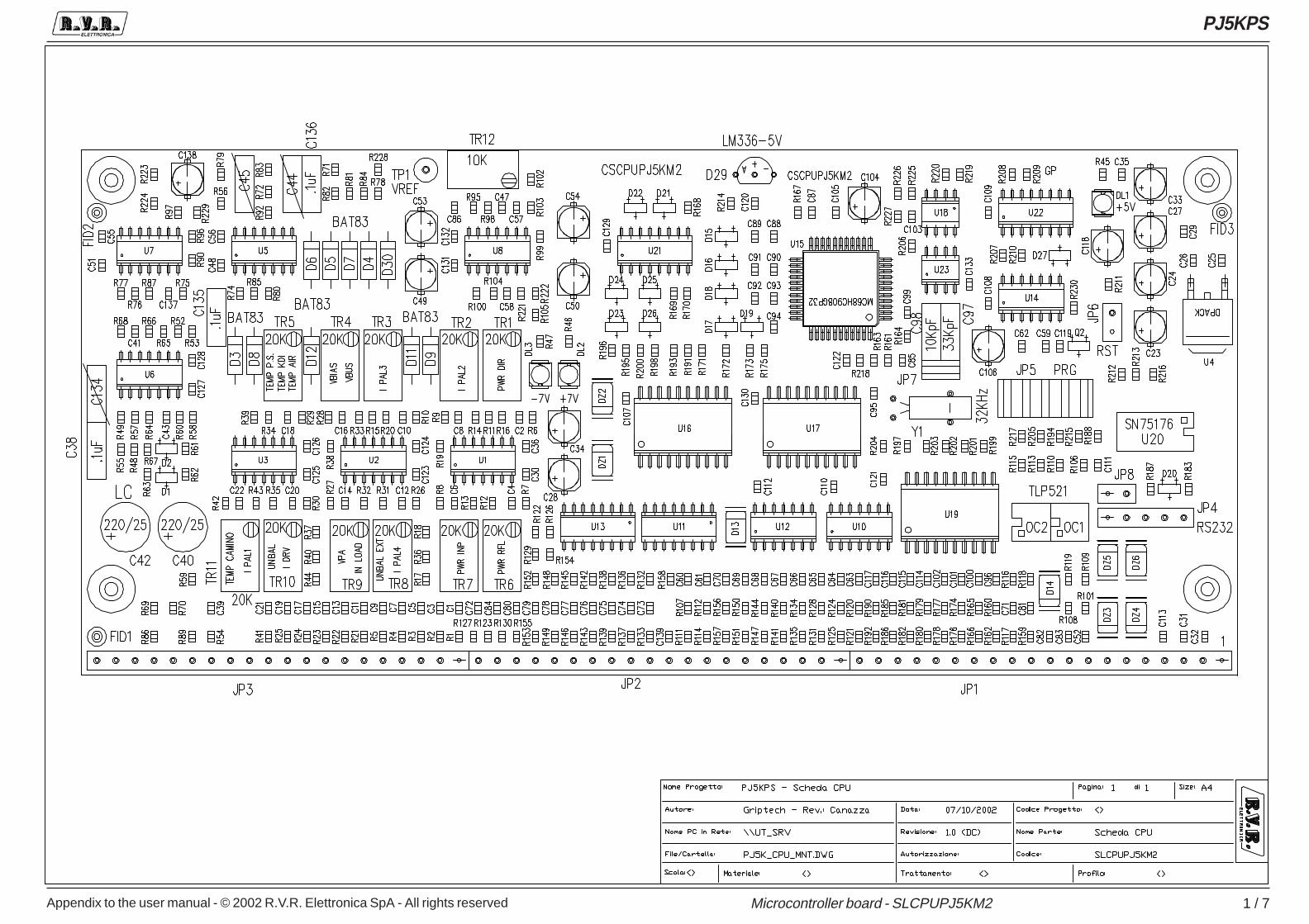
Appendix to the user manual - © 2002 R.V.R. Elettronica SpA - All rights reserved
PJ5KPS
1 / 7Microcontroller board - SLCPUPJ5KM2
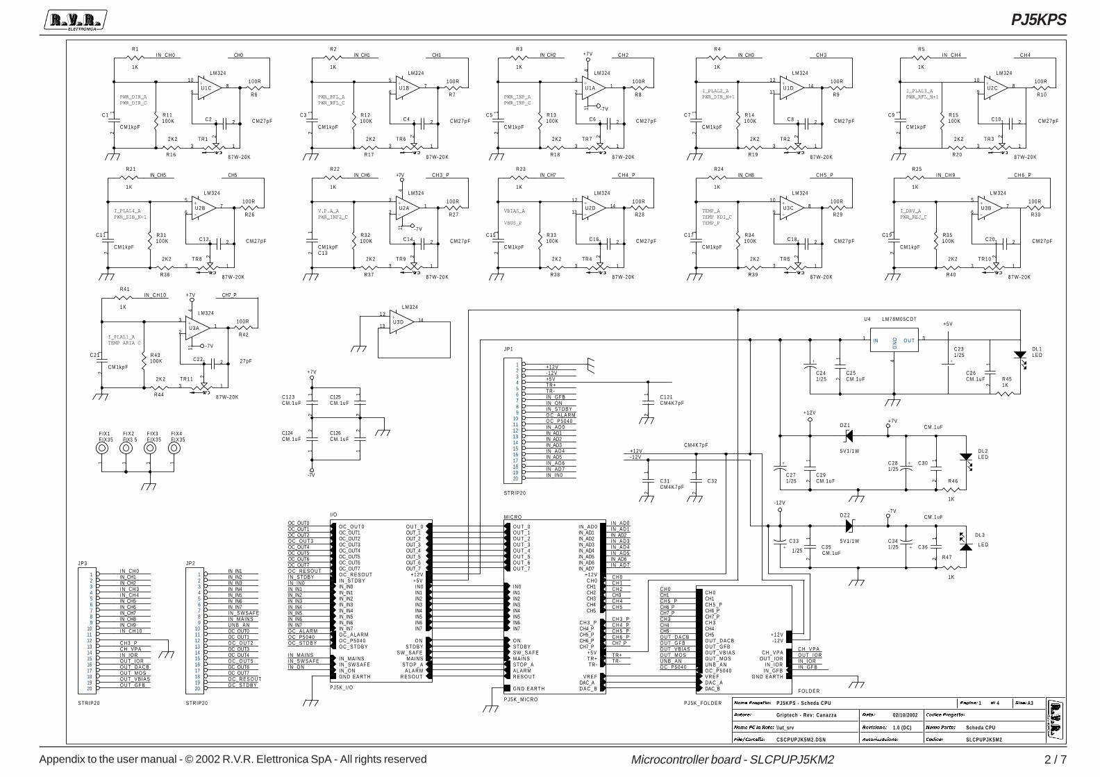
Appendix to the user manual - © 2002 R.V.R. Elettronica SpA - All rights reserved
PJ5KPS
2 / 7Microcontroller board - SLCPUPJ5KM2
PWR_DIR_CPWR_DIR_A
PWR_RFL_CPWR_RFL_A
PWR_INP_CPWR_INP_A
V.P.A_APWR_INP2_C
VBIAS_APWR_REJ_C
VBUS_P TEMP_P
TEMP_ATEMP KDI_C
I_DRV_A
I_PLAL1_A
I_PLAL2_APWR_DIR_N+1
I_PLAL3_APWR_RFL_N+1
I_PLAL4_APWR_SIB_N+1
TEMP ARIA C
PJ5KPS - Scheda CPU 4
Griptech - Rev: Canazza
Scheda CPU
SLCPUPJK5M2
\\ut_srv
CSCPUPJK5M2.DSN
02/10/2002
A31
1.0 (DC)
� � � � � � � � � � � � �
� � � � � � � � � � � � � � � � � � �
� � � � � � � � � � � �
� � � � � � � � � � � � �
� � � � �
� � � � � � � �
� � � � � �
� � � � � � � � � �
� � � � � � � � � � �
� � � � � � � � � ��
M I C R O
PJ5K_MICRO
IN_AD0IN_AD1IN_AD2
IN_AD4IN_AD5
IN_AD7
IN_AD3
IN_AD6
O U T _ 0
O U T _ 3O U T _ 4O U T _ 5
O U T _ 7
O U T _ 2O U T _ 1
O U T _ 6
C H 0CH1CH2CH3CH4CH5
C H 3 _ PCH4_PCH5_PCH6_PCH7_P
IN0IN1IN2IN3IN4IN5IN6IN7
O NSTDBYS W _ S A F E
STOP_AA L A R MR E S O U T
MAINS TR+TR-
V R E F
D A C _ BDAC_A
+12V
+5V
G N D E A R T H
I/O
PJ5K_I /O
OUT_0OUT_1
OUT_3OUT_4OUT_5OUT_6OUT_7
OUT_2
O C _ O U T 0OC_OUT1OC_OUT2OC_OUT3OC_OUT4OC_OUT5OC_OUT6OC_OUT7
IN0IN1IN2IN3IN4IN5IN6IN7
IN_IN0IN_IN1IN_IN2IN_IN3IN_IN4IN_IN5IN_IN6IN_IN7
S T O P _ AA L A R M
R E S O U T
O NSTDBY
S W _ S A F EMAINS
OC_P5040O C _ S T D B Y
O C _ R E S O U T
IN_MAINSI N _ S W S A F EIN_ONG N D E A R T H
+5V+12V
O C _ A L A R M
IN_STDBY
F O L D E R
PJ5K_FOLDER
V R E FD A C _ ADAC_B
IN_GFB
O U T _ D A C BO U T _ G F BOUT_VBIASOUT_MOSU N B _ A N
+12V-12V
G N D E A R T HOC_P5040
C H _ V P AOUT_ IOR
IN_IOR
C H 0CH1C H 5 _ PCH6_PCH7_PC H 3CH4CH5
IN_CH0 IN_CH1 IN_CH2 IN_CH3
IN_CH5 IN_CH6 IN_CH7 IN_CH8
IN_CH10
O C _ O U T 5
OC_OUT3OC_OUT4
O C _ S T D B Y
O C _ O U T 2
OC_OUT6OC_OUT7
OC_OUT1OC_OUT0
O C _ R E S O U T
IN_IN0
IN_IN1IN_IN2IN_IN3IN_IN4IN_IN5IN_IN6IN_IN7
IN_AD7
IN_AD5
IN_AD3IN_AD2
IN_CH4
IN_CH9IN_CH8IN_CH7
IN_CH5
IN_AD6
IN_AD1
IN_CH0
IN_CH6
IN_CH2IN_CH1
IN_CH10
IN_AD4
IN_CH3
IN_MAINS
C H _ V P A
O U T _ D A C BOUT_MOS
O U T _ G F B
I N _ S W S A F E
+12V-12V
O C _ O U T 3OC_OUT4
OC_OUT1OC_OUT0
OC_OUT6OC_OUT5
OC_OUT7
OC_OUT2
IN_IN0IN_IN1IN_IN2IN_IN3IN_IN4IN_IN5IN_IN6IN_IN7
O C _ R E S O U T
OC_P5040O C _ S T D B Y
IN_MAINSI N _ S W S A F EIN_ON
O U T _ D A C BO U T _ G F BOUT_VBIASOUT_MOSU N B _ A N
C H 5
C H 4 _ P
IN_AD1
C H 3 _ P
CH7_P
TR-
IN_AD4
C H 4 _ P
IN_AD7
C H 5 _ P
TR+
C H 0
CH5
CH1
C H 5 _ P
IN_AD3
C H 2CH0
IN_AD0
IN_AD2
IN_AD6
C H 4
C H 6 _ P
C H 2
C H 3 _ P
CH7_P
C H 3
IN_AD5
C H 1
CH3
O C _ A L A R MU N B _ A N
IN_STDBY
OC_P5040
C H _ V P A
IN_CH4 C H 4
IN_CH9 C H 6 _ P
OUT_ IORIN_IOROUT_ IOR
IN_IOR
IN_GFB
C H 0CH1C H 5 _ PCH6_PCH7_PC H 3CH4CH5
+12V-12V
IN_GFB
O C _ A L A R MIN_STDBYIN_ON
+5V
OUT_VBIAS
C H 3 _ P
TR-TR+
IN_AD0OC_P5040 +7V
-7V
-12V
+12V
+5V
-7V
+7V
-7V
+7V
+7V
-7V
-7V
+7V
R21
1K
R15100K
TR4
8 7 W - 2 0K
13
2
C 5
CM1kpF
12
C17
CM1kpF
12
R14100K
R47
1K
R31100K
C13CM1kpF
12
R20
2K2
R28
100R +
-U 3 C
LM32410
98
R 3
1K
R24
1K
R19
2K2
U 4 LM78M05CDT
4
1 3
GN
DIN O U T
R36
2K2
R22
1K
TR3
87W-20K
13
2
C16 CM27pF1 2
JP2
STRIP20
123456789
1011121314151617181920
R13100K
R34100K
TR2
87W-20K
13
2
TR8
8 7 W - 2 0K
13
2
R32100K
R10
100R
R16
2K2
+
-U 2 D
LM32412
1314
TR1
8 7 W - 2 0K
13
2
R18
2K2
C 3
CM1kpF
12
C 2 CM27pF1 2
R39
2K2
R 9
100R+
-U 1 A
LM3243
21
411
R26
100R
R37
2K2
C10 CM27pF1 2
TR7
8 7 W - 2 0K
13
2
R 2
1K
TR5
87W-20K
13
2
C 8 CM27pF1 2R11100K
C12 CM27pF1 2
TR9
87W-20K
13
2
+
-U 2 A
LM3243
21
411
R 8
100R
R12100K
R29
100R
+
-U 1 D
LM32412
1314
+
-U 2 B
LM3245
67
R27
100R
+
C271/25
C 6 CM27pF1 2
C19
CM1kpF
12
R17
2K2
C18 CM27pF1 2C14 CM27pF1 2
+
-U 1 C
LM32410
98
R25
1K
R451K
TR6
87W-20K
13
2
+
-U 3 A
LM3243
21
411
+
-U 2 C
LM32410
98
R35100K
JP3
STRIP20
123456789
1011121314151617181920
R 7
100R
C125CM.1uF
12
R40
2K2
C 4 CM27pF1 2
R 6
100R
C126CM.1uF
12
TR10
8 7 W - 2 0K
13
2
+
-U 1 B
LM3245
67
R46
1K
C123CM.1uF
12
R30
100R
C124CM.1uF
12
C20 CM27pF1 2
+
-U 3 B
LM3245
67
C21
CM1kpF
12
R41
1K
FIX1FIX35
1
C 1
CM1kpF
12
F IX2FIX3 5
1
C121C M 4 K 7 p F
12
+
C33
1/25
R43100K
FIX3FIX35
1
DZ2
5V1 /1W
FIX4FIX35
1
DL2L E D
R44
2K2
DZ1
5V1 /1W
C35CM.1uF
12
TR11
87W-20K
13
2
C32
C M 4 K 7 p F
12
+
C241/25
C31C M 4 K 7 p F
12
R 1
1K
C36
CM.1uF
12
DL3
L E D
R42
100R
+
C231/25
+
C341/25
C22 27pF1 2
C25CM.1uF
12
+C281/25
C29CM.1uF
12
JP1
STRIP20
123456789
1011121314151617181920
+
-U 3 D
LM32412
1314
C26CM.1uF
12
C30
CM.1uF
12
C15
CM1kpF
12
R23
1K
C 9
CM1kpF
12
R33100K
C 7
CM1kpF
12
C11
CM1kpF
12
R 5
1K
DL1L E D
R38
2K2
R 4
1K
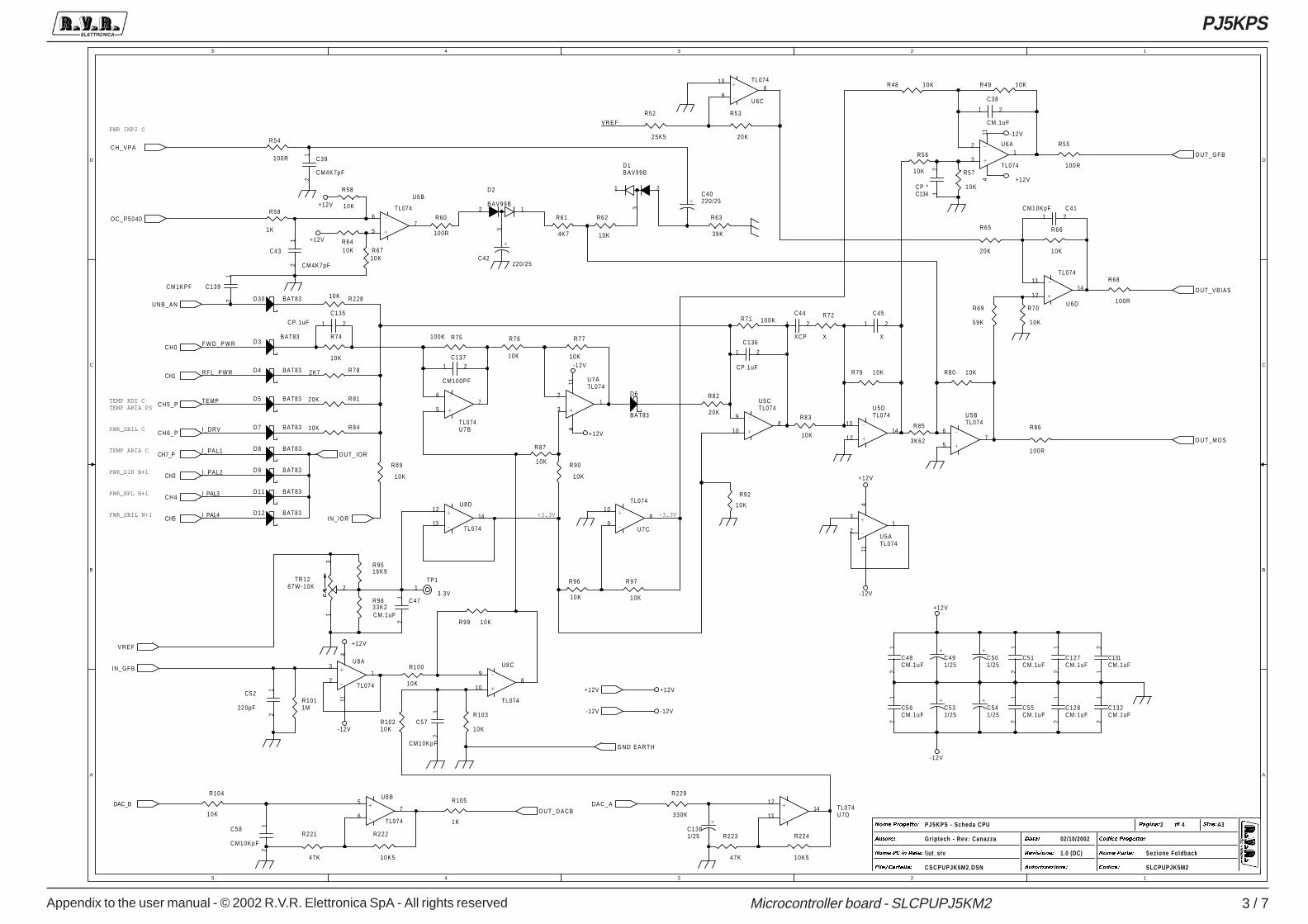
Appendix to the user manual - © 2002 R.V.R. Elettronica SpA - All rights reserved
PJ5KPS
3 / 7Microcontroller board - SLCPUPJ5KM2
5
5
4
4
3
3
2
2
1
1
D D
C C
B B
A A
-3.3V+3.3V
PWR_DIR N+1
PWR_RFL N+1
PWR_SBIL N+1
TEMP KDI CTEMP ARIA PS
TEMP ARIA C
PWR INP2 C
PWR_SBIL C
PJ5KPS - Scheda CPU 4
Gr iptech - Rev: Canazza
Sezione Foldback
SLCPUPJK5M2
\\ut_srv
CSCPUPJK5M2.DSN
02/10/2002
A32
1.0 (DC)
� � � � � � � � � � � � �
� � � � � � � � � � � � � � � � � � �
� � � � � � � � � � � �
� � � � � � � � � � � � �
� � � � �
� � � � � � � �
� � � � � �
� � � � � � � � � �
� � � � � � � � � � �
� � � � � � � � � ��
R F L _ P W R
F W D _ P W R
I_PAL1
I_PAL4
I_PAL3
TEMP
I_PAL2
I_DRV
VREF
+12V
-12V
-12V
+12V
-12V
+12V
+12V
-12V
+12V
+12V
-12V
-12V
+12V
+12V
C48CM.1uF
12
C56CM.1uF
12
R68
100R
C134CP *
12
TP1
3.3V1
C44
XCP
1 2
+
-
U8B
TL074
5
67
+
C42220/25
R72
X
R223
47K
R54
100R
C131CM.1uF
12
R229
330K
R53
20K
C132CM.1uF
12
R9833K2
R1011M
D30 BAT83
D4 BAT83
C137
CM100PF
1 2
R103
10K
R83
10K
C58
CM10KpF
12
R782K7
R221
47K
R10210K
+
-
U 5 DTL074
12
1314
+
- U 7 C
TL07410
98
R76
10K
R97
10K
D2
BAV99B2
3
1
C136
CP.1uF
1 2
+
- U 6 C
TL07410
98
R8410K
R56
10K
R92
10K
R52
25K5
R69
59K
R105
1K
R222
10K5
R66
10K
+
-
U8A
TL074
3
21
411
D3BAT83
D5 BAT83
C57
CM10KpF
12
+
-
U7ATL074
3
21
411
R74
10K
R79 10K
C128CM.1uF
12
+
-
U 8 D
TL074
12
1314
R8120K
R59
1K
R104
10K
R96
10K
R61
4K7
R55
100R
+C1381/25
C52
220pF
12
C139CM1KPF
12
C127CM.1uF
12
R63
39K
R58
10K
C43
CM4K7pF
12
D1BAV99B
2
3
1
+C40220/25
+
-
U6B
TL074
5
67
+
-
U7BTL074
5
67
R75100K
R6410K
R60
100R
D6
BAT83
R6710K
+
-
U 6 D
TL074
12
1314
R70
10K
C39
CM4K7pF
12
R71 100KC135
CP.1uF 1 2
R62
10K
+C491/25
D8 BAT83
R82
20K
R9516K9
R77
10K
+C501/25
R90
10KD9 BAT83
TR1287W-10K
13
2
C38
CM.1uF
1 2
+
- U5ATL074
3
21
411
R87
10K
+C531/25
+
- U6A
TL0743
21
411
R100
10K
D11 BAT83
C45
X
1 2
C41CM10KpF1 2
R224
10K5
C47
CM.1uF
12
R49 10K
+C541/25
D12 BAT83
C51CM.1uF
12
R99 10K
+
-
U 8 C
TL074
10
98
+
-U 7 DTL074
12
1314
R65
20K
+
-
U 5 CTL074
10
98
R57
10K
D7 BAT83 R86
100R
+
-
U5BTL074
5
67
R85
3K62
C55CM.1uF
12
R80 10K
R48 10K
R89
10K
R22810K
VREF
DAC_ADAC_B
IN_GFB
O U T _ D A C B
O U T _ G F B
OUT_VBIAS
O U T_MOS
+12V
-12V
GND EARTH
OC_P5040
CH_VPA
OUT_ IOR
IN_IOR
C H 0
CH1
CH5_P
CH7_P
C H 4
CH5
CH3
CH6_P
U N B _ A N
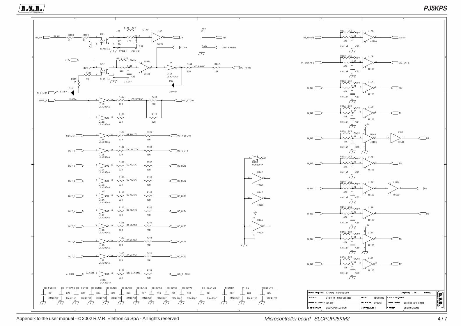
Appendix to the user manual - © 2002 R.V.R. Elettronica SpA - All rights reserved
PJ5KPS
4 / 7Microcontroller board - SLCPUPJ5KM2
5
5
4
4
3
3
2
2
1
1
D D
C C
B B
A A
PJ5KPS - Scheda CPU 4
Gr iptech - Rev: Canazza
Sezione I /O digitale
SLCPUPJK5M2
\\ut_srv
CSCPUPJK5M2.DSN
02/10/2002
A33
1.0 (DC)
� � � � � � � � � � � � �
� � � � � � � � � � � � � � � � � � �
� � � � � � � � � � � �
� � � � � � � � � � � � �
� � � � �
� � � � � � � �
� � � � � �
� � � � � � � � � �
� � � � � � � � � � �
� � � � � � � � � ��
O C _ O U T 0 C
OC_OUT1C
OC_OUT2C
OC_OUT3C
OC_OUT4C
OC_OUT5C
OC_OUT6C
OC_OUT7C
O C _ A L A R M CALAR M
OC_P5040C
OC_P5040C
O C _ O U T 0 C OC_OUT1C OC_OUT2C OC_OUT3C OC_OUT4C OC_OUT5C OC_OUT6C OC_OUT7CO C _ S T O P A C
OC_STOPAC
IN_ONO C _ A L A R M C
R E S O U T C
IN_STDBY
IN_STDBY
G N D
R E S O U T C
IN_ON
+12V
+5V+5V
+5V
+5V
+5V
+5V
+5V
+5V
+5V
+5V
+5V
+5V
+5V
+5V
+5V
+5V
D13
1N4004
R109
1K
U12B
40106
3 4
U11BULN2004A
2 15
R133
22R
C81
CM4K7pF
12
R134 2K2
O C 1
TLP521-1
1
2
4
3
R122
22R
C75
CM4K7pF
12
U14A
40106
1 2
147
U13AULN2004A
1 16
9
R153
22R
C66CM.1uF
12
R156 2K2
R150 2K2
C78
CM4K7pF
12
U11DULN2004A
4 13
R142
22R
U12E
40106
11 10
C70CM.1uF
12
R137
22R
U12F
40106
13 12
R118
1K
C69CM.1uF
12
R135
47K
U14E
40106
11 10
O C 2
TLP521-1
1
2
4
3
U11CULN2004A
3 14
U14F
40106
13 12
C72
CM4K7pF
12
R157
47K
U14C
40106
5 6
R113 2K2
R151
47K
U13EULN2004A
5 12
R115
47K
U13GULN2004A
7 10
U11EULN2004A
5 12
R139
22R
R155
22R
C62
CM.1uF
12
R158
22R
R132
22R
U10F
40106
13 12
C71
CM4K7pF
12
U13BULN2004A
2 15
C82
CM4K7pF
12
R127
22R
R128 2K2
R106 2K2
C76
CM4K7pF
12
U13DULN2004A
4 13
R145
22R
C83
CM4K7pF
12
C65CM.1uF
12
R144 2K2
R152
22R
R123
22R
U12A
40106
1 2
147
C68CM.1uF
12
C73
CM4K7pF
12
C61CM.1uF
12
R126
22R
C79
CM4K7pF
12
R131
47K
U14B
40106
3 4
R159
22R
R110
47K
R143
22R
U10E
40106
11 10
U11AULN2004A
1 16
9
D14
1N4004
R117
22R
R147
47K
C59
CM.1uF
12
R112 2K2
U11FULN2004A
6 11
R107 2K2
R116
22R
R114
47K
R136
22R
C60CM.1uF
12
U12D
40106
9 8
U13FULN2004A
6 11
R111
47K
U13CULN2004A
3 14
R154
22R
U10D
40106
9 8
R146
22R
R108
1K
R148
22R
R124 2K2
C77
CM4K7pF
12
R140 2K2
C74
CM4K7pF
12
C64CM.1uF
12
R121
47K
C67CM.1uF
12
U10B
40106
3 4
C63CM.1uF
12
U11GULN2004A
7 10U12C
40106
5 6
R125
47K
R130
22R
R120 2K2
R138
22RR141
47K
U10A
40106
1 2
147
R149
22R
U10C
40106
5 6
C80
CM4K7pF
12
JP8
STRIP 2
12
C84
CM4K7pF
12
R1191K
R129
22R
O U T _0
O U T _1
O U T _2
O U T _3
O U T _4
O U T _5
O U T _6
O U T _7
O C _ O U T 0
OC_OUT1
OC_OUT2
OC_OUT3
OC_OUT4
OC_OUT5
OC_OUT6
OC_OUT7
O C _ A L A R M
IN0
IN1
IN2
IN3
IN4
IN5
IN6
IN7
IN_IN0
IN_IN1
IN_IN2
IN_IN3
IN_IN4
IN_IN5
IN_IN6
IN_IN7
R E S O U T O C _ R E S O U T
O N
STDBY
S W _ S A F E
MAINS
STOP_A OC_STDBY
ALARM
IN_MAINS
I N _ S W S A F E
IN_ON
IN_STDBY
OC_P5040
+5V
GND EARTH
+12V
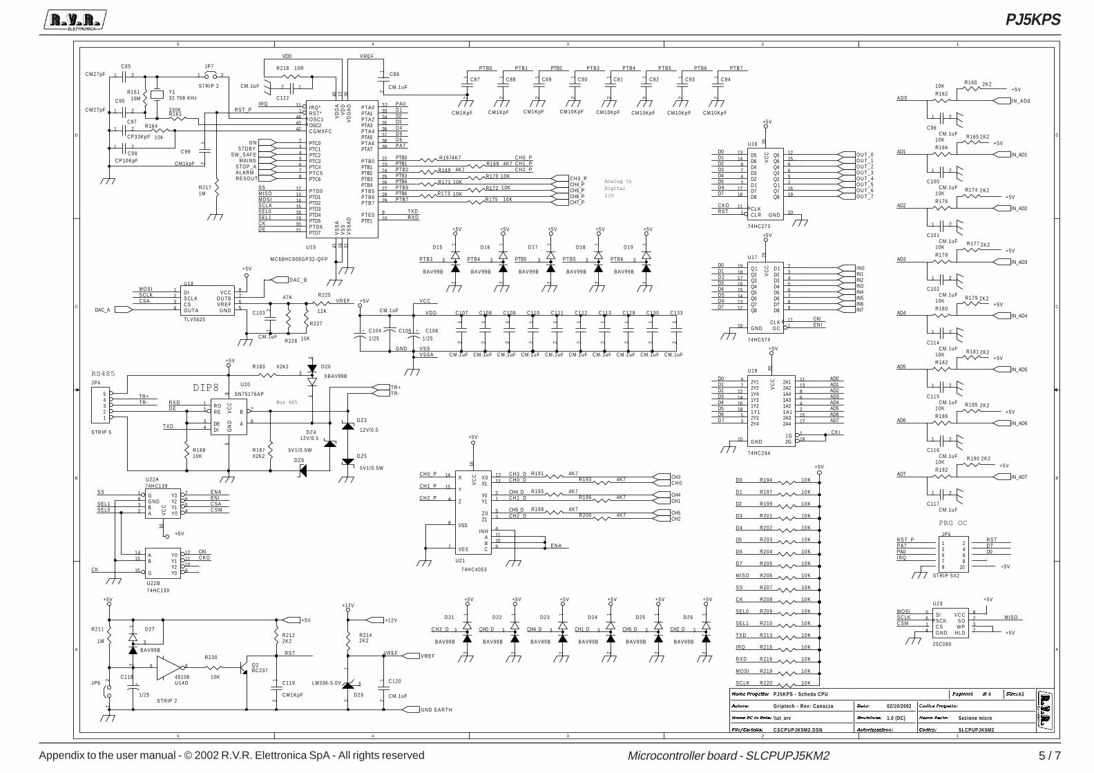
Appendix to the user manual - © 2002 R.V.R. Elettronica SpA - All rights reserved
PJ5KPS
5 / 7Microcontroller board - SLCPUPJ5KM2
5
5
4
4
3
3
2
2
1
1
D D
C C
B B
A A
Analog InDigitalI/O
Bus 485
PRG OC
DIP8RS485
PJ5KPS - Scheda CPU 4
Gr iptech - Rev: Canazza
Sezione micro
SLCPUPJK5M2
\\ut_srv
CSCPUPJK5M2.DSN
02/10/2002
A34
1.0 (DC)
� � � � � � � � � � � � �
� � � � � � � � � � � � � � � � � � �
� � � � � � � � � � � �
� � � � � � � � � � � � �
� � � � �
� � � � � � � �
� � � � � �
� � � � � � � � � �
� � � � � � � � � � �
� � � � � � � � � ��
D7D6
R S TC K O
D6D7
D1
D3
D4
D2
D3D2D1D0
D5
D4
D0
D5
SEL1
C K
AD0
AD1
AD5AD4
AD2
AD7
AD3
AD6
AD0
AD1
AD2
AD3
AD4
AD5
AD6
AD7
MOSISCLKC S M
D6
D2
D5
SS
C K
D3
SEL1
D0
SEL0
D1
MISO
D4
TXD
D7
IRQ
R X D
R S TD7D0
RST_PPA7PA0IRQ
D6
D3
D7
CKI
D2
D4
D1D0
ENICKI
D5MOSI
C S ASCLK
MISO
CH3_D CH0_D CH4_D CH1_D CH5_D CH2_D
PTB3 PTB4 PTB5 PTB5 PTB6
MOSI
D4D3
R X D
D5
D2
VREF
SCLK
VREF
D6
MISO
SEL0
PTB5
PTB3
PTB1CH0_P
TXD
PTB6PTB4PTB1 PTB2
D E
PTB7
SS
PTB5PTB0
PA0
CH2_P
PTB7
CH1_P
PTB3
IRQ
C K
D1
SEL1
PA7
PTB2
PTB0
PTB4
PTB6
V C C
VDD
CH2_P
CH0_D
CH4_D
VSS
CH1_P
CH1_D
CH5_D
V D D
G N D
CH2_D
VSSA
CH3_D
E N A
CH0_P
TXD
R S T
D ER X D
TR+T R -
E N A
C S MC S AENI
CKI
SS
SEL0
RST_P
MOSI
SCLK
VREF
C K O
+5V
+5V
+5V
+5V
+5V
+12V
+5V
+5V
+5V
+5V
+5V
+5V
+5V+5V +5V +5V +5V +5V +5V
+5V +5V +5V +5V +5V
+5V
+5V
+5V
+5V
+5V
+5V
+5V
+5V
+5V
R173 10K
C92
CM10KpF
12
R201 10K
R211
1M
R191 4K7
D25
BAV99B
2
3
1
JP4
STRIP 5
12345
R175 10K
R226
47K
R202 10K
C98CP10KpF
1 2
R187X2K2
C88
CM1KpF
12
R203 10K
U17
74HC574
23456789
111
1918171615141312
20
10
D1D2D3D4D5D6D7D8
CLKO C
Q 1Q2Q3Q4Q5Q6Q7Q8
VC
C
G N D
R2171M
U16
74HC273
3478
1314
1718
111
2569
1215
1619
20
10
D1D2D3D4
D5D6
D7D8
CLKC L R
Q 1Q2Q3Q4
Q5Q6
Q7Q8
VC
C
G N D
U19
74HC244
2468
1113
1517
119
18161412
97
53
20
10
1A11A21A31A4
2A12A2
2A32A4
1 G2G
1Y11Y21Y31Y4
2Y12Y2
2Y32Y4
VC
C
G N D
R218 10R
R204 10K
R193 4K7
R205 10K
R207 10K
R181 2K2
D15
BAV99B
2
3
1
R220 10K
R17810KU15
MC68HC908GP32-QFP
32
23
3311
34
24
35
1
36
25
37
40
38
26
39
41
27
17
28
16
29
3031
910
121314151819
23456
22
2021
444342
78
PTA0
PTB1
PTA1IRQ*
PTA2
PTB2
PTA3
RST*
PTA4
PTB3
PTA5
VD
DA
PTA6
PTB4
PTA7
VS
SA
PTB5
VD
D
PTB6
VS
S
PTB7
VD
DA
DV
SS
AD
PTE0PTE1
PTD0PTD1PTD2PTD3PTD4PTD5
PTC0PTC1PTC2PTC3PTC4
PTB0
PTD6PTD7
O S C 1OSC2C G M X F C
PTC5PTC6
C99
CM1kpF
12
C115CM.1uF
1 2
C93
CM10KpF
12
D16
BAV99B
2
3
1
R219 10K
C102CM.1uF
1 2
R225
12K
R18210K
D17
BAV99B
2
3
1 R177 2K2
JP5
STRIP 5X2
1 23 45 67 89 10
U18
TLV5625
234
1 8765
SCLKC SO U T A
DI V C CO U T BVREFG N D
R16110M
Q 2BC237
R230
10K
R163330K
R185 2K2
D18
BAV99B
2
3
1
R164
10k
C89
CM1KpF
12
R206 10K
DZ412V/0.5
R160 2K2
DZ6
5V1/0 .5W C116CM.1uF
1 2
R16210K
D19
BAV99B
2
3
1
C86
CM.1uF
12
R2142K2
Y132.768 KHz
DZ3
12V/0.5
C87
CM1KpF
12
C105
CM.1uF
R1674K7
D29
LM336-5.0V
2
3
1
C96CM.1uF
1 2
DZ5
5V1/0 .5W
+ C1041/25
C122
CM.1uF 12
R18610K
R17610K
+ C1061/25
R183 X2K2
R195 4K7
D23
BAV99B
2
3
1
+C118
1/25
R190 2K2
C101CM.1uF
1 2
U23
25C080
561
237
8
4
SIS C KC S
S OW P
H L D
V C C
G N D
C133
CM.1uF
12
R196 4K7
C94
CM10KpF
12
R197 10K
C117CM.1uF
1 2
R174 2K2
R227
10K
C119
CM1KpF
12
C103
CM.1uF
12
R19210K
R208 10K
D26
BAV99B
2
3
1
R179 2K2
C90
CM10KpF
12
D22
BAV99B
2
3
1
C130
CM.1uF
12
R16610K
C114CM.1uF
1 2
R209 10K
C85CM27pF 1 2
C97
CP33KpF
1 2
C100CM.1uF
1 2
R18010K
U22B74HC139
1413
15
1211109
AB
G
Y0Y1Y2Y3
C120
CM.1uF
12
R198 4K7
R216 10K
R165 2K2
R210 10K
D20
XBAV99B
2
3
1
R200 4K7
D24
BAV99B
2
3
1
U14D40106
9 8
C107
CM.1uF
12
R213 10K
C112
CM.1uF
12
C108
CM.1uF
12
C91
CM10KpF
12
D27
BAV99B
2
3
1
R168 4K7
JP6
STRIP 2
12
C113
CM.1uF
12
C95
CM27pF 1 2
C109
CM.1uF
12
R215 10K
C129
CM.1uF
12
R169 4K7
C110
CM.1uF
12
R170 10K
C111
CM.1uF
12
R2122K2
U20
SN75176AP
12
34
7
6
58
R OR E
DEDI
B
A
GN
DV
CC
R171 10K
R18810K
R194 10K
JP7
STRIP 2
1 2
U21
74HC4053
1213
21
53
611109
14
15
4
16
7
8
X0X1
Y0Y1
Z0Z1
INHABC
X
Y
Z
VC
C
VEE
VSS
U22A74HC139
23
1
4567
8
16
AB
G
Y0Y1Y2Y3
G N D
VC
C
R172 10K
R199 10K
D21
BAV99B
2
3
1
IN_AD0
IN_AD2
IN_AD3
IN_AD4
IN_AD5
IN_AD6
IN_AD1
IN_AD7
O U T _ 0O U T _ 1O U T _ 2O U T _ 3O U T _ 4O U T _ 5O U T _ 6O U T _ 7
IN0IN1IN2IN3IN4IN5IN6IN7
O NSTDBY
S W _ S A F EMAINS
STOP_AALARMR E S O U T
TR+TR-
VREF
DAC_B
DAC_A
CH3_PCH4_PCH5_PCH6_PCH7_P
C H 0
CH1
CH2
CH3
CH4
CH5
+12V+5V
GND EARTH
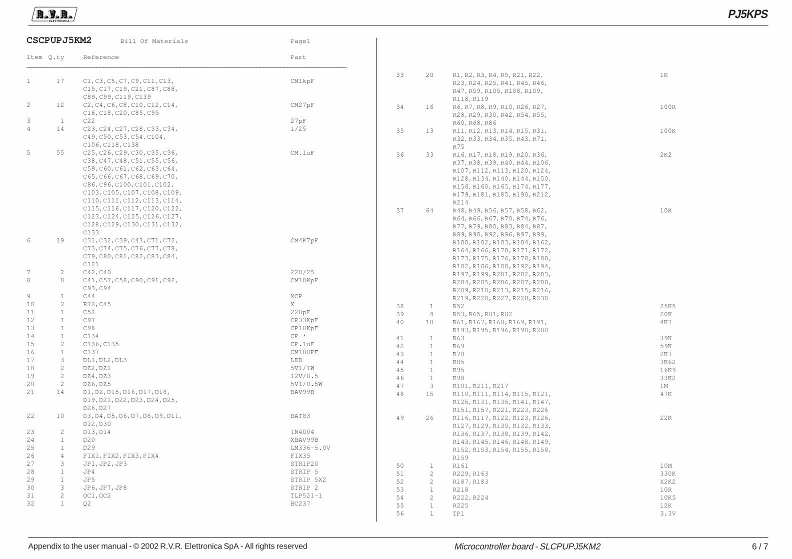
Appendix to the user manual - © 2002 R.V.R. Elettronica SpA - All rights reserved
PJ5KPS
6 / 7Microcontroller board - SLCPUPJ5KM2
CSCPUPJ5KM2 Bill Of Materials Page1
Item Q.ty Reference Part____________________________________________________________________________________________
1 17 C1,C3,C5,C7,C9,C11,C13, CM1kpFC15,C17,C19,C21,C87,C88,C89,C99,C119,C139
2 12 C2,C4,C6,C8,C10,C12,C14, CM27pFC16,C18,C20,C85,C95
3 1 C22 27pF4 14 C23,C24,C27,C28,C33,C34, 1/25
C49,C50,C53,C54,C104,C106,C118,C138
5 55 C25,C26,C29,C30,C35,C36, CM.1uFC38,C47,C48,C51,C55,C56,C59,C60,C61,C62,C63,C64,C65,C66,C67,C68,C69,C70,C86,C96,C100,C101,C102,C103,C105,C107,C108,C109,C110,C111,C112,C113,C114,C115,C116,C117,C120,C122,C123,C124,C125,C126,C127,C128,C129,C130,C131,C132,C133
6 19 C31,C32,C39,C43,C71,C72, CM4K7pFC73,C74,C75,C76,C77,C78,C79,C80,C81,C82,C83,C84,C121
7 2 C42,C40 220/258 8 C41,C57,C58,C90,C91,C92, CM10KpF
C93,C949 1 C44 XCP10 2 R72,C45 X11 1 C52 220pF12 1 C97 CP33KpF13 1 C98 CP10KpF14 1 C134 CP *15 2 C136,C135 CP.1uF16 1 C137 CM100PF17 3 DL1,DL2,DL3 LED18 2 DZ2,DZ1 5V1/1W19 2 DZ4,DZ3 12V/0.520 2 DZ6,DZ5 5V1/0.5W21 14 D1,D2,D15,D16,D17,D18, BAV99B
D19,D21,D22,D23,D24,D25,D26,D27
22 10 D3,D4,D5,D6,D7,D8,D9,D11, BAT83D12,D30
23 2 D13,D14 1N400424 1 D20 XBAV99B25 1 D29 LM336-5.0V26 4 FIX1,FIX2,FIX3,FIX4 FIX3527 3 JP1,JP2,JP3 STRIP2028 1 JP4 STRIP 529 1 JP5 STRIP 5X230 3 JP6,JP7,JP8 STRIP 231 2 OC1,OC2 TLP521-132 1 Q2 BC237
33 20 R1,R2,R3,R4,R5,R21,R22, 1KR23,R24,R25,R41,R45,R46,R47,R59,R105,R108,R109,R118,R119
34 16 R6,R7,R8,R9,R10,R26,R27, 100RR28,R29,R30,R42,R54,R55,R60,R68,R86
35 13 R11,R12,R13,R14,R15,R31, 100KR32,R33,R34,R35,R43,R71,R75
36 33 R16,R17,R18,R19,R20,R36, 2K2R37,R38,R39,R40,R44,R106,R107,R112,R113,R120,R124,R128,R134,R140,R144,R150,R156,R160,R165,R174,R177,R179,R181,R185,R190,R212,R214
37 64 R48,R49,R56,R57,R58,R62, 10KR64,R66,R67,R70,R74,R76,R77,R79,R80,R83,R84,R87,R89,R90,R92,R96,R97,R99,R100,R102,R103,R104,R162,R164,R166,R170,R171,R172,R173,R175,R176,R178,R180,R182,R186,R188,R192,R194,R197,R199,R201,R202,R203,R204,R205,R206,R207,R208,R209,R210,R213,R215,R216,R219,R220,R227,R228,R230
38 1 R52 25K539 4 R53,R65,R81,R82 20K40 10 R61,R167,R168,R169,R191, 4K7
R193,R195,R196,R198,R20041 1 R63 39K42 1 R69 59K43 1 R78 2K744 1 R85 3K6245 1 R95 16K946 1 R98 33K247 3 R101,R211,R217 1M48 15 R110,R111,R114,R115,R121, 47K
R125,R131,R135,R141,R147,R151,R157,R221,R223,R226
49 26 R116,R117,R122,R123,R126, 22RR127,R129,R130,R132,R133,R136,R137,R138,R139,R142,R143,R145,R146,R148,R149,R152,R153,R154,R155,R158,R159
50 1 R161 10M51 2 R229,R163 330K52 2 R187,R183 X2K253 1 R218 10R54 2 R222,R224 10K555 1 R225 12K56 1 TP1 3.3V
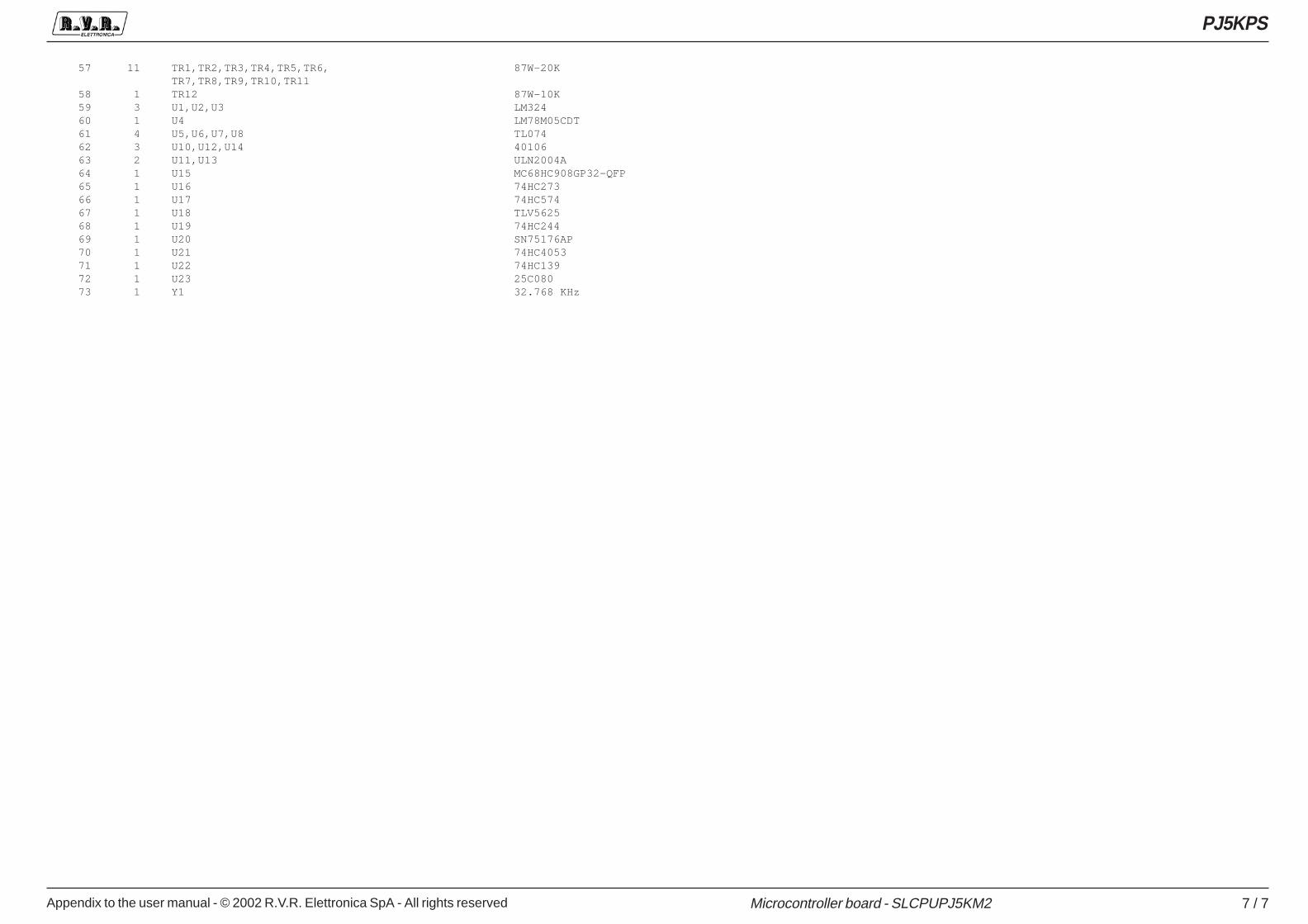
Appendix to the user manual - © 2002 R.V.R. Elettronica SpA - All rights reserved
PJ5KPS
7 / 7Microcontroller board - SLCPUPJ5KM2
57 11 TR1,TR2,TR3,TR4,TR5,TR6, 87W-20KTR7,TR8,TR9,TR10,TR11
58 1 TR12 87W-10K59 3 U1,U2,U3 LM32460 1 U4 LM78M05CDT61 4 U5,U6,U7,U8 TL07462 3 U10,U12,U14 4010663 2 U11,U13 ULN2004A64 1 U15 MC68HC908GP32-QFP65 1 U16 74HC27366 1 U17 74HC57467 1 U18 TLV562568 1 U19 74HC24469 1 U20 SN75176AP70 1 U21 74HC405371 1 U22 74HC13972 1 U23 25C08073 1 Y1 32.768 KHz
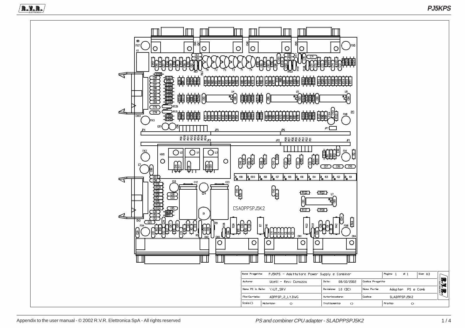
Appendix to the user manual - © 2002 R.V.R. Elettronica SpA - All rights reserved
PJ5KPS
1 / 4PS and combiner CPU adapter - SLADPPSPJ5K2
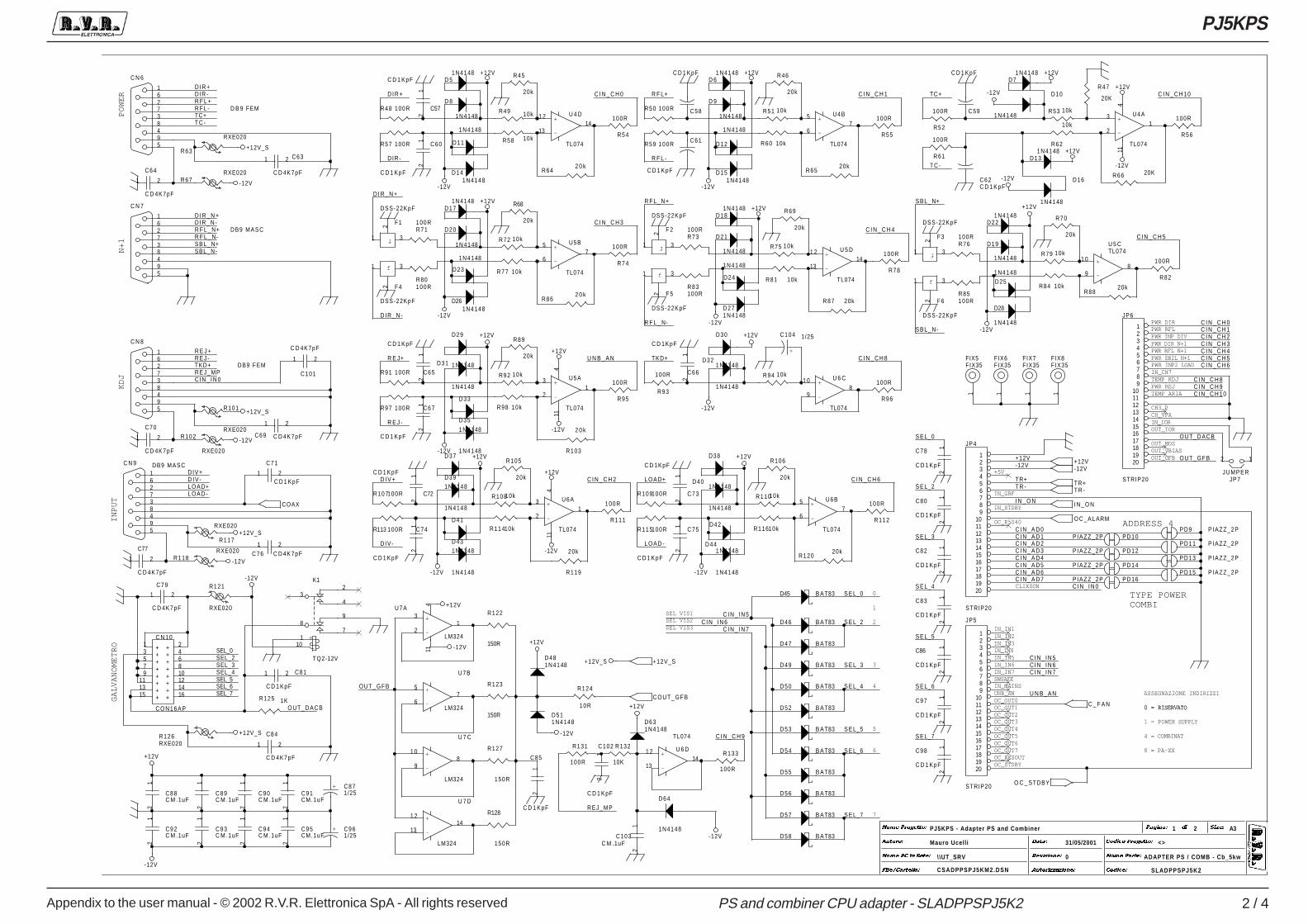
Appendix to the user manual - © 2002 R.V.R. Elettronica SpA - All rights reserved
PJ5KPS
2 / 4PS and combiner CPU adapter - SLADPPSPJ5K2
TYPE POWERCOMBI
IN_IN4
PWR DIR
PWR INP DIV
1
4 = COMBINAT
OUT_GFBOUT_VBIAS
IN_MAINS
IN_IN5
+5V
IN_IN2
TEMP KDJ
1 = POWER SUPPLY
IN_CH7
0 = RISERVATOOC_OUT1
CH3_P
IN_IN1
OC_OUT4
0 = RISERVATO
OC_OUT5
OC_OUT2
OUT_IOR
PWR RFL
OC_P5040
IN_STDBY
PWR INP2 LOAD
OC_OUT7
ADDRESS 4
IN_IOR
IN_IN3
CLIXSON
PWR SBIL N+1
8 = PA-XX
IN_IN7
0
PWR RFL N+1
IN_IN6
ASSEGNAZIONE INDIRIZZI
OC_RESOUT
TEMP ARIA
OC_OUT6
PWR DIR N+1
OUT_MOS
OC_OUT3
PWR REJ
CH_VPA
IN_GBF
POWER
KDJ
INPUT
N+1
SWSAFE
UNB_AN
OC_STDBY
OC_OUT0GALVANOMETRO
2
3
4
5
6
7
SEL VIS1SEL VIS2SEL VIS3
PJ5KPS - Adapter PS and Combiner
<>
2
Mauro Ucell i
ADAPTER PS / COMB - Cb_5kw
SLADPPSPJ5K2
\\UT_SRV
CSADPPSPJ5KM2.DSN
31/05/2001
A31
0
� � � � � � � � � � � � �
� � � � � � � � � � � � � � � � � � �
� � � � � � � � � � � �
� � � � � � � � � � � � �
� � � � �
� � � � � � � �
� � � � � �
� � � � � � � � � �
� � � � � � � � � � �
� � � � � � � � � ��
DIR-
D I R +
C I N _ A D3
C I N _ I N 5
-12V
U N B _ A N
C I N _ A D1
C I N _ C H 6
C I N _ A D2
I N _ O N
C I N _ C H 8
C I N _ C H 5
C I N _ C H 2
C I N _ A D0
C I N _ C H 4
OUT_DACB
C I N _ C H 10
C I N _ I N 7
C I N _ I N 0
C I N _ C H 1
C I N _ A D4
C I N _ C H 0
C I N _ C H 9
C I N _ I N 6
+12V
T R -TR+
C I N _ C H 3
C I N _ A D7C I N _ A D6
OUT_GFB
C I N _ A D5
C I N _ C H 0D I R +DIR-R F L +R F L -TC+T C -
R F L+
R F L -
C I N _ C H 1 TC+
T C -
C I N _ C H 10
C I N _ C H 6
R E J -
L O A D+
TKD+
DIV+C I N _ C H 2D I V -
L O A D -D IV -
TKD+R E J+R E J +
D I V + L O A D+
R E J - C I N _ C H 8
L O A D -
REJ_MP
D I R _ N -
R F L _ N-SBL_N+
D I R _ N +
SBL_N-
R F L _N+D I R _ N - C I N _ C H 3
D I R _ N +R F L_N+
C I N _ C H 4
R F L _ N-
SBL_N+
C I N _ C H 5
S B L _ N -
SEL_4
OUT_GFB
SEL_3
S E L_2
SEL_2
SEL_6
SEL_0
SEL_7
SEL_5
OUT_DACB
C I N _ I N 6
S E L_4
S E L_3
S E L_5
S E L_0
S E L_6
C I N _ I N 7
S E L_6
S E L_0
S E L_7
S E L_5
S E L_2
S E L_7
S E L_3
S E L_4
C I N _ I N 5
U N B _ A N
C I N _ C H 9
REJ_MP
C I N _ I N 0
-12V
+12V
+12V_S
+12V_S
+12V_S
+12V_S
+12V
-12V
+12V_S
-12V
+12V
-12V
+12V
-12V
+12V
-12V
+12V
-12V
+12V
-12V
+12V
-12V
+12V
-12V
+12V
-12V
+12V
-12V
+12V
+12V
-12V
-12V
-12V
-12V
-12V
+12V
-12V
+12V
-12V
+12V
-12V
+12V
-12V
-12V
+12V
R94 10k+
-
U5A
TL074
3
21
411
R60 10k
JP5
STRIP20
123456789
1011121314151617181920
C90C M .1uF
12
R89
20k
R124
10R
R68
20k
C71
C D 1 KpF1 2
C85
C D 1 KpF
12
C103C M .1uF
12
R107100R
R85100R
D23
1N4148
D22
1N4148
C79
C D 4K7pF
1 2
C102
C D 1 KpF
12
JP4
STRIP20
123456789
1011121314151617181920
+
-
U 4 B
TL074
5
67
R12020k
FIX5FIX35
1
D47 B A T83
D271N4148
D30
1N4148
D58 B A T83
D39
1N4148
R47
20K
R11610k
R101
RXE020
R50 100R
+
-
U 7 C
LM324
1 0
98
+
-
U 5 D
TL074
1 2
1314
f
F4
DSS-22KpF
1 3
2
R82
100R
R111
100R +
-
U 6 B
TL074
5
67
D56 B A T83
R106
20k
C95CM.1uF
12
C59
C D 1 KpF
PD16P I AZZ_2P
C77
C D 4K7pF
1 2
R642 0 k
C76 C D 4K7pF1 2
R132
10K
R67RXE020
C69 C D 4K7pF
1 2
R63
RXE020
C91CM.1uF
12
+ C871/25
D20
1N4148
D24
1N4148
C70
C D 4K7pF
1 2
C88C M .1uF
12
R133
100R
C N 6
D B 9 FEM
594837261
D37
1N4148
R117
RXE020
D19
1N4148
R126RXE020
C78
C D 1 KpF
12
C N 8
DB9 FEM
594837261
R72 10k
P D 1 1 P I AZZ_2P
C57
C D 1 KpF
12
C75
C D 1 KpF
12
R97 100R
D35
1N4148
D44
1N4148
R81 10k
R75 10k
C98
C D 1 KpF
12
P D 1 5 P I AZZ_2P
D45 B A T83
+
K1
TQ2-12V
32
4
89
71
10
R105
20k
R10810k
R73100R
R58 10k
R98 10k
D151N4148
C80
C D 1 KpF
12
+
-
U 5 CTL074
1 0
98
R11010k
R49 10k
C84
C D 4K7pF
1 2
R112
100R
C83
C D 1 KpF
12
R51 10k
D12
1N4148
D21
1N4148
D33
1N4148
D42
1N4148
D64
1N4148
R55
100R
R45
20k
D171N4148
C64
C D 4K7pF
1 2
R102RXE020
R6520k
C92C M .1uF
12
D481N4148
JP6
STRIP20
123456789
1011121314151617181920
C63
C D 4K7pF
1 2
R69
20k
R54
100R
FIX7FIX35
1
D131N4148
R103
2 0 k
D 8
1N4148
R121
RXE020
D10
1N4148
C67
C D 1 KpF
12
R74
100R
C81
C D 1 KpF
1 2
D141N4148
R84 10k
R87 20k
R127
150R
D50 B A T83
R79 10k
+
-
U 4 A
TL074
3
21
411
R71100R
R113 100R
R48 100R
C97
C D 1 KpF
12
R76100R
R57 100R D11
1N4148
C101
C D 4K7pF
1 2
R52
100R
D31
1N4148
D40
1N4148
R95
100R
+
-
U5B
TL074
5
67
R109100R
D181N4148
+
-
U 7 D
LM324
1 2
1314
C66
C D 1KpF
12
C62C D 1 KpF
C72
C D 1 KpF 12
C N 7
DB9 MASC
594837261
R96
100R
C65
C D 1 KpF
12
f
F 5
DSS-22KpF
1 3
2
R119
20k
R46
20k
R62
10k
C74
C D 1 KpF
12
R125 1K
PD12P I AZZ_2P
D 9
1N4148
+
-
U 7 B
LM324
5
67
+
C104 1/25
D54 B A T83
FIX6FIX35
1
C93C M .1uF
12
R66 20K
R862 0 k
D71N4148
R70
20k
f
F 2
DSS-22KpF
1 3
2
C58
C D 1 KpF
C73
C D 1KpF
12
+
-
U 6 D
TL074
1 2
1314
C61
C D 1 KpF
D28
1N4148
+ C961/25
C89C M .1uF
12
C N 9 DB9 MASC
594837261
D43
1N4148
JP7J U M P E R
12
f
F1
DSS-22KpF
1 3
2
+
-
U 6 A
TL074
3
21
411
R8820k
R123
150RD52 B A T83
C N 10
C O N 1 6 A P
13579
111315
246810121416
++++++++
++++++++
R131
100R
D631N4148
R61
100R
R83100R
R92 10k
R11410k
D 51N4148
R77 10k
R91 100R
D29
1N4148
D38
1N4148
D511N4148
R115100R
D16
1N4148
D49 B A T83
D41
1N4148
+
-
U 4 D
TL074
1 2
1314
D 61N4148
D46 B A T83
D251N4148
D57 B A T83
R53 10k
C60
C D 1 KpF
12
C82
C D 1 KpF
12
R56
100R
FIX8FIX35
1
R118RXE020
D32
1N4148
R122
150R
R128
150R
f
F6
DSS-22KpF
1 3
2
PD14P I AZZ_2P
D261N4148
R78
100R
R93
100R
D55 B A T83
R80100R
C94C M .1uF
12
f
F3
DSS-22KpF
1 3
2
R59 100R
P D 9 P I AZZ_2P
P D 1 3 P I AZZ_2P
+
-
U 7 A
LM324
3
21
411
D53 B A T83
+
-
U 6 C
TL074
1 0
98
PD10P I AZZ_2P
C86
C D 1 KpF
12
TR+T R -
I N _ O N
O C _ A L ARM
+12V-12V
C _ F A NCOUT_GFB
O C _ STDBY
COAX
+12V_S
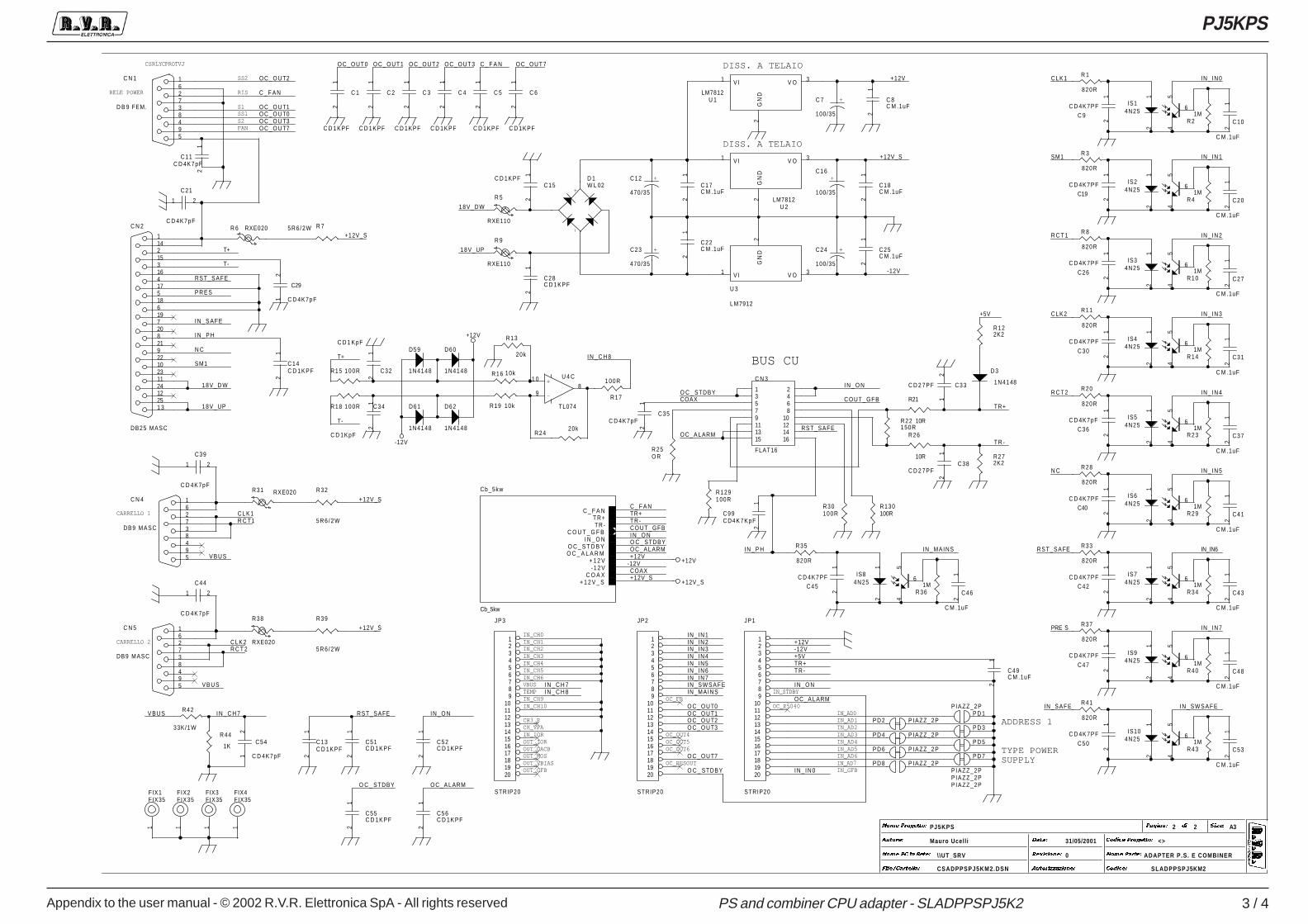
Appendix to the user manual - © 2002 R.V.R. Elettronica SpA - All rights reserved
PJ5KPS
3 / 4PS and combiner CPU adapter - SLADPPSPJ5K2
IN_AD0IN_AD1IN_AD2IN_AD3IN_AD4IN_AD5IN_AD6
IN_GFB
SS1S1
SS2
S2FAN
RIS
IN_CH1IN_CH2IN_CH3
IN_CH6
IN_CH4IN_CH5
IN_CH9IN_CH10
OC_RESOUT
CH_VPACH3_P
OUT_GFB
OUT_DACBOUT_MOS
IN_CH0
OUT_VBIAS
RELE POWER
OC_FB
IN_IOROUT_IOR
ADDRESS 1
IN_AD7
TYPE POWERSUPPLY
IN_STDBY
OC_P5040
OC_OUT4OC_OUT5
CSRLYCPROTVJ
BUS CU
VBUSTEMP
CARRELLO 1
CARRELLO 2
OC_OUT6
DISS. A TELAIO
DISS. A TELAIO
PJ5KPS
<>
2
Mauro Ucell i
ADAPTER P.S. E COMBINER
SLADPPSPJ5KM2
\\UT_SRV
CSADPPSPJ5KM2.DSN
31/05/2001
A32
0
� � � � � � � � � � � � �
� � � � � � � � � � � � � � � � � � �
� � � � � � � � � � � �
� � � � � � � � � � � � �
� � � � �
� � � � � � � �
� � � � � �
� � � � � � � � � �
� � � � � � � � � � �
� � � � � � � � � ��
Cb_5kw
Cb_5kw
C _ F A NT R +TR-
C O U T _ G F BI N _ O N
O C _ S T D B YO C _ A L A R M
+ 1 2 V- 1 2 V
C O A X+ 1 2 V _ S
+12V_S
-12V
18V_DW
I N _ I N 0CLK1
SM1 I N _ I N 1
R C T 1 I N _ I N 2
CLK2 I N _ I N 3
R C T 2 I N _ I N 4
N C I N _ I N 5
IN_IN6RST_SAFE
I N _ I N 7PRE S
I N _ S W S A F EIN_SAFE
O C _ O U T7
O C _ O U T0O C _ O U T1
O C _ O U T2
O C _ O U T3
I N _ S A F E
SM1
N C
RST_SAFE
I N _ C H 7V B U S
I N _ MAINS
+5V
18V_UP
P R E S
18V_UP
18V_D W
T R -
RST_SAFE
O C _ STDBY
O C _ A L ARM
I N _ O N
O C _ STDBY O C _ A L ARM
RST_SAFE I N _ O N
+12V
OC_OUT0 OC_OUT1 OC_OUT2 OC_OUT3 OC_OUT7
+12V_S
V B U S
+12V_S
R C T1C L K 1
CLK2
V B U S
+12V_S
R C T 2
T+
T-
O C _ A L ARM
+12V
+5VTR+
I N _ I N 0
I N _ O N
T R -
-12V
O C _ O U T1
O C _ O U T3
I N _ I N 7
O C _ STDBY
O C _ O U T2
O C _ O U T7
IN_MAINS
O C _ O U T0
I N _ S W S A F E
I N _ I N 6I N _ I N 5
I N _ I N 2
I N _ I N 4I N _ I N 3
I N _ I N 1
I N _ C H 8I N _ C H 7
COAX
I N _ C H 8
T-
T+
COUT_GFB
C _ F A N
C _ F A N
C _ F A NTR+T R -COUT_GFB
TR+
I N _ O NO C _ STDBYO C _ A L ARM+12V
-12VCOAX+12V_S
I N _ P H
I N _ P H +12V
-12V
+12V
+12V_S
C 8C M .1uF
12
JP1
STRIP20
123456789
1011121314151617181920
C21
C D 4K7pF
1 2
+C12
470/35
R11
820R
C28C D 1KPF
12
C42C D 4K7PF
12
U 1LM7812
1
2
3V I
GN
D
V O
R15 100R
C33C D 2 7PF
12
C30
C D 4K7PF
12
P D 1P I AZZ_2P
R 5
RXE110
R30100R
R26
10R
C19C D 4K7PF
12
IS14N25
12
54
6
C22C M .1uF
12
U 2LM7812
1
2
3V I
GN
D
V O
IS54N25
12
54
6
R42
33K/1 W
R37
820R
R122K2
C11C D 4K7pF
12
R272K2
C 1
C D 1KPF
12
IS34N25
12
54
6
P D 4 P I AZZ_2P
FIX1FIX35
1
R13
20k
IS44N25
12
54
6
P D 3
P I AZZ_2P
C40C D 4K7PF
12
R129100R
R28
820R
IS24N25
12
54
6
P D 7
P I AZZ_2P
R401M
R 1
820R
C N 3
FLAT16
13579111315
2468
10121416
R25O R
D60
1N4148
R21M
C43
C M .1uF
12
C54
C D 4K7pF12
C27
C M .1uF
12
R101M
P D 8 P I AZZ_2P
R21
10R
R431M
C 9C D 4K7PF
12
+C23
470/35
U 3
L M 7912
1
2
3V I
GN
D
V O
R 8
820R
R361MC44
C D 4K7pF
1 2
C37
C M .1uF
12
R31 RXE020
R231M
C26
C D 4K7PF
12
FIX4FIX35
1R 75 R 6 / 2 W
C32
C D 1 KpF
12
+C16
100/35
IS94N25
12
54
6
C41
C M .1uF
12
F IX2FIX35
1
R 9
RXE110
C45C D 4K7PF
12
C52C D 1KPF
12
D3
1N4148
R341M
-+
D 1W L 02
R32
5 R 6 / 2 W
R141M
C 6
C D 1KPF
12
IS104N25
12
54
6
D61
1N4148R22150R
P D 6 P I AZZ_2P
R 6 RXE020
R 3
820R
C N 2
DB25 MASC
1 3251224112310229218207196185174163152141
C35C D 4K7pF
12
R2420k
C17C M .1uF
12
C48
C M .1uF
12
C99CD4K7KpF
12
C10
C M .1uF
12
C13C D 1KPF
12
C51C D 1KPF
12
C15C D 1KPF
12
C 3
C D 1KPF
12
C34
C D 1KpF
12
JP3
STRIP20
123456789
1011121314151617181920
C 2
C D 1KPF
12
C31
C M .1uF
12
C49C M .1uF
12
R35
820R
R19 10k
R130100R
C53
C M .1uF
12
C N 5
DB9 MASC
594837261
+
-
U 4 C
TL074
1 0
98
C46
C M .1uF
12
IS84N25
12
54
6
C N 4
DB9 MASC
594837261
R16 10k
C 4
C D 1KPF
12
C14C D 1KPF
12
D62
1N4148
R44
1K
R33
820R
C 5
C D 1KPF
12
C N 1
D B 9 FEM.
594837261
C56C D 1KPF
12
R17
100R
R18 100R
C55C D 1KPF
12
D59
1N4148
C38C D 2 7PF
12
C36C D 4K7pF
12
C39
C D 4K7pF
1 2
+C 7
100/35
IS64N25
12
54
6
R39
5 R 6 / 2 W
R38
RXE020
C18C M .1uF
12 C20
C M .1uF
12
R41
820R
C47
C D 4K7PF
12
C25C M .1uF
12
JP2
STRIP20
123456789
1011121314151617181920
R291M
R41M
C50
C D 4K7PF
12
IS74N25
12
54
6
+C24
100/35
R20
820R
FIX3FIX35
1
P D 2 P I AZZ_2P
P D 5
P I AZZ_2P
C29
C D 4K7pF12
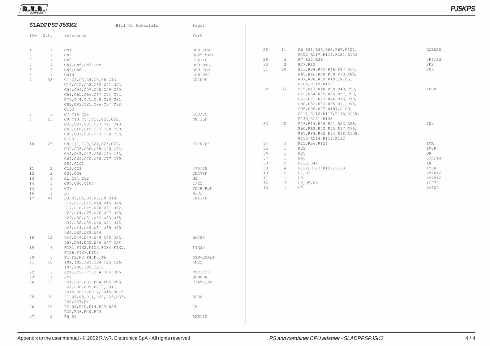
Appendix to the user manual - © 2002 R.V.R. Elettronica SpA - All rights reserved
PJ5KPS
4 / 4PS and combiner CPU adapter - SLADPPSPJ5K2
SLADPPSPJ5KM2 Bill Of Materials Page1
Item Q.ty Reference Part____________________________________________________________________________________________
1 1 CN1 DB9 FEM.2 1 CN2 DB25 MASC3 1 CN3 FLAT164 4 CN4,CN5,CN7,CN9 DB9 MASC5 2 CN6,CN8 DB9 FEM6 1 CN10 CON16AP7 38 C1,C2,C3,C4,C5,C6,C13, CD1KPF
C14,C15,C28,C32,C51,C52,C55,C56,C57,C58,C59,C60,C61,C65,C66,C67,C71,C72,C73,C74,C75,C78,C80,C81,C82,C83,C85,C86,C97,C98,C102
8 3 C7,C16,C24 100/359 25 C8,C10,C17,C18,C20,C22, CM.1uF
C25,C27,C31,C37,C41,C43,C46,C48,C49,C53,C88,C89,C90,C91,C92,C93,C94,C95,C103
10 26 C9,C11,C19,C21,C26,C29, CD4K7pFC30,C35,C36,C39,C40,C42,C44,C45,C47,C50,C54,C63,C64,C69,C70,C76,C77,C79,C84,C101
11 2 C12,C23 470/3512 2 C33,C38 CD27PF13 3 K1,C34,C62 NC14 3 C87,C96,C104 1/2515 1 C99 CD4K7KpF16 1 D1 WL0217 47 D3,D5,D6,D7,D8,D9,D10, 1N4148
D11,D12,D13,D14,D15,D16,D17,D18,D19,D20,D21,D22,D23,D24,D25,D26,D27,D28,D29,D30,D31,D32,D33,D35,D37,D38,D39,D40,D41,D42,D43,D44,D48,D51,D59,D60,D61,D62,D63,D64
18 12 D45,D46,D47,D49,D50,D52, BAT83D53,D54,D55,D56,D57,D58
19 8 FIX1,FIX2,FIX3,FIX4,FIX5, FIX35FIX6,FIX7,FIX8
20 6 F1,F2,F3,F4,F5,F6 DSS-22KpF21 10 IS1,IS2,IS3,IS4,IS5,IS6, 4N25
IS7,IS8,IS9,IS1022 6 JP1,JP2,JP3,JP4,JP5,JP6 STRIP2023 1 JP7 JUMPER24 16 PD1,PD2,PD3,PD4,PD5,PD6, PIAZZ_2P
PD7,PD8,PD9,PD10,PD11,PD12,PD13,PD14,PD15,PD16
25 10 R1,R3,R8,R11,R20,R28,R33, 820RR35,R37,R41
26 10 R2,R4,R10,R14,R23,R29, 1MR34,R36,R40,R43
27 2 R5,R9 RXE110
28 11 R6,R31,R38,R63,R67,R101, RXE020R102,R117,R118,R121,R126
29 3 R7,R32,R39 5R6/2W30 2 R27,R12 2K231 20 R13,R24,R45,R46,R47,R64, 20k
R65,R66,R68,R69,R70,R86,R87,R88,R89,R103,R105,R106,R119,R120
32 37 R15,R17,R18,R30,R48,R50, 100RR52,R54,R55,R56,R57,R59,R61,R71,R73,R74,R76,R78,R80,R82,R83,R85,R91,R93,R95,R96,R97,R107,R109,R111,R112,R113,R115,R129,R130,R131,R133
33 22 R16,R19,R49,R51,R53,R58, 10kR60,R62,R72,R75,R77,R79,R81,R84,R92,R94,R98,R108,R110,R114,R116,R132
34 3 R21,R26,R124 10R35 1 R22 180R36 1 R25 OR37 1 R42 33K/1W38 2 R125,R44 1K39 4 R122,R123,R127,R128 150R40 2 U1,U2 LM781241 1 U3 LM791242 3 U4,U5,U6 TL07443 1 U7 LM324
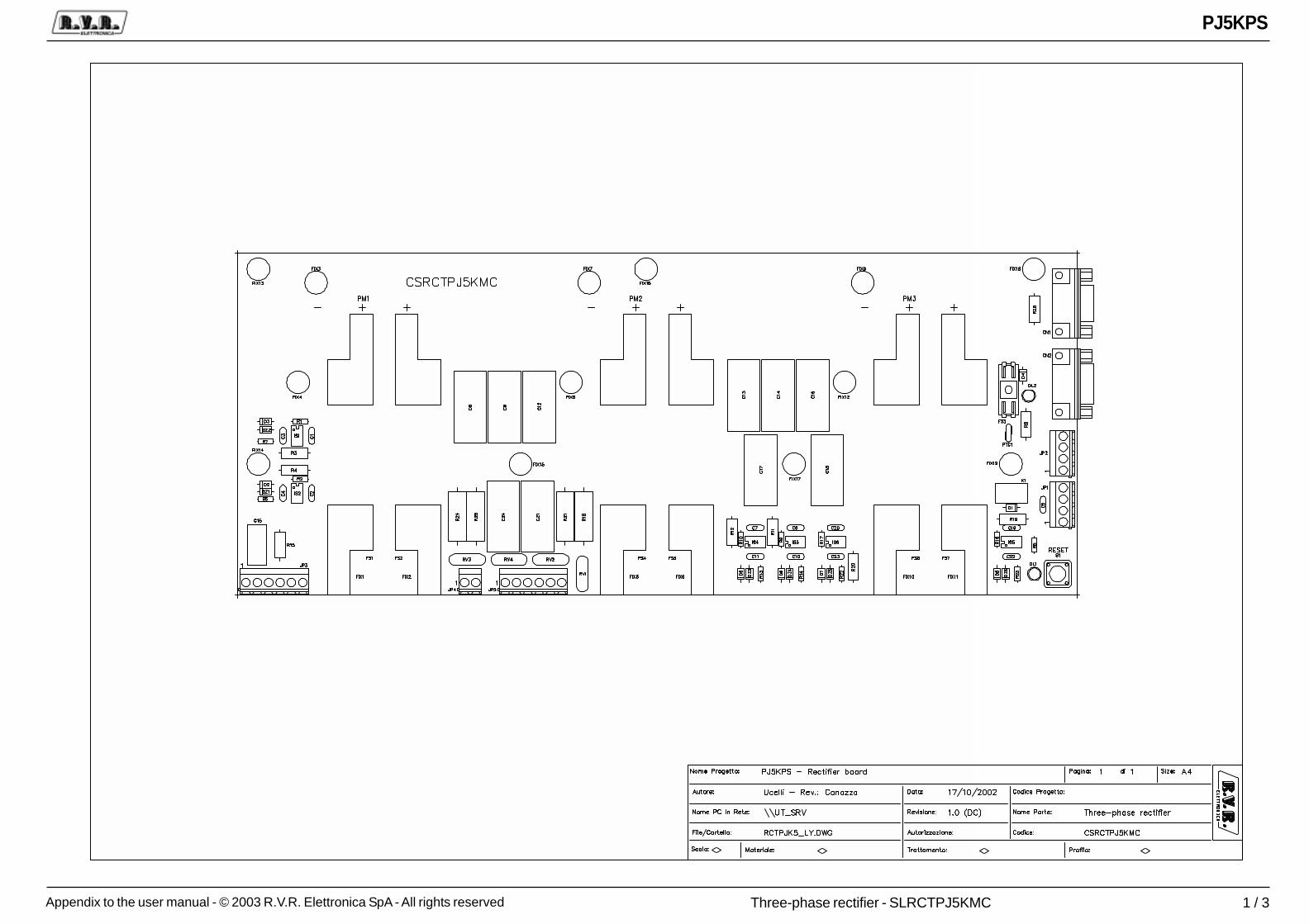
Appendix to the user manual - © 2003 R.V.R. Elettronica SpA - All rights reserved
PJ5KPS
1 / 3Three-phase rectifier - SLRCTPJ5KMC
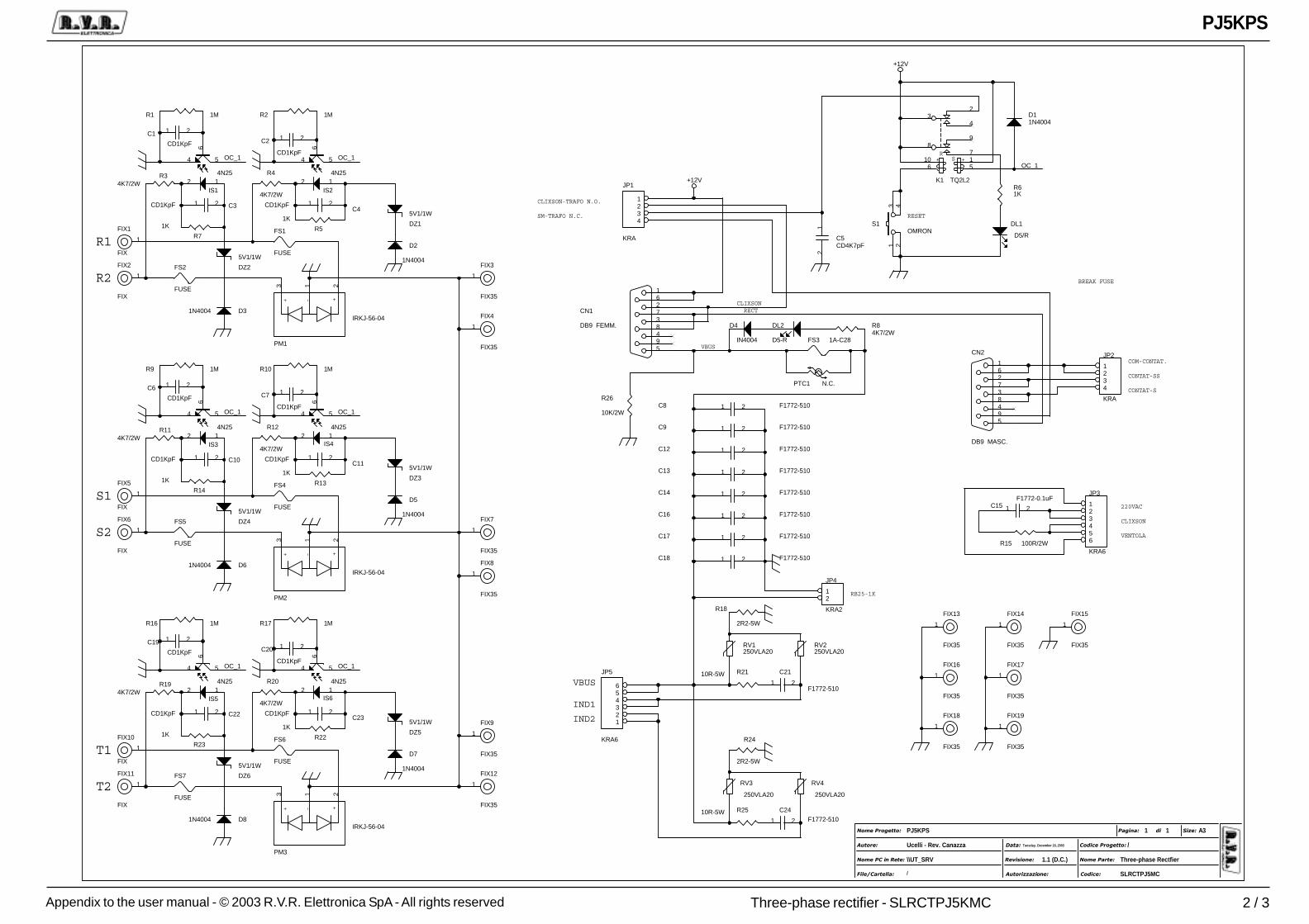
Appendix to the user manual - © 2003 R.V.R. Elettronica SpA - All rights reserved
PJ5KPS
2 / 3Three-phase rectifier - SLRCTPJ5KMC
R1
R2
S2
S1
T2
T1
VENTOLA
CLIXSON
VBUS
220VAC
CLIXSON
SM-TRAFO N.C.
RECT
CLIXSON-TRAFO N.O.
CONTAT-S
BREAK FUSE
CONTAT-SS
COM-CONTAT.
RESET
RB25-1K
VBUS
IND2
IND1
\\UT_SRV Three-phase Rectfier
SLRCTPJ5MC
1.1 (D.C.)
PJ5KPS
/Ucelli - Rev. Canazza
11 A3
Tuesday, December 16, 2003
/
�����������
����� ������������
������ �������
����� ������
���
���������
�����
���������
�������������
������ ������
OC_1OC_1
OC_1OC_1
OC_1OC_1
OC_1
+12V
+12V
D4
IN4004
C10CD1KpF 1 2
FS5
FUSE
FIX8
FIX35
1
C9 F1772-5101 2
FIX17
FIX35
1
C5CD4K7pF
12
DZ1
5V1/1W
CN1
DB9 FEMM.
594837261
FIX19
FIX35
1
C16 F1772-5101 2
C22CD1KpF 1 2
FS7
FUSE
R34K7/2W
FIX15
FIX35
1
R61K
R4
4K7/2W
JP1
KRA
1234
R7
1K
FIX7
FIX35
1
R114K7/2W
RV3
250VLA20
R2110R-5W
FIX9
FIX35
1
+ +-
PM2
IRKJ-56-04
213
DZ4
5V1/1W
IS4
4N2512
54
6
JP2
KRA
1234
FIX12
FIX35
1
R15 100R/2W
R194K7/2W
C8 F1772-5101 2
R10 1M
S1OMRON
13
24
DZ6
5V1/1W
IS6
4N2512
54
6
+ +R
S
K1 TQ2L2
32
4
89
7106
15
C14 F1772-5101 2
FIX5
FIX
1
R17 1M
C1
CD1KpF
1 2
D2
1N4004
JP4
KRA2
12
R14
1K
FIX10
FIX
1
DL1
D5/R
CN2
DB9 MASC.
594837261
DZ2
5V1/1W
R23
1K
C4CD1KpF 1 2
RV4
250VLA20
FIX6
FIX
1
R2 1M
D61N4004C18 F1772-5101 2
FIX11
FIX
1
IS1
4N2512
54
6
C24F1772-5101 2
C13 F1772-5101 2
C7
CD1KpF
1 2
D81N4004
FS3 1A-C28
C15F1772-0.1uF
1 2
C6
CD1KpF
1 2
JP5
KRA6
123456
R9 1M
C20
CD1KpF
1 2
R26
10K/2W
+ +-
PM3
IRKJ-56-04
213
FS2
FUSE
R18
2R2-5W
C19
CD1KpF
1 2RV1250VLA20
R16 1M
R13
1KDZ3
5V1/1W
IS3
4N2512
54
6
FIX1
FIX
1
R24
2R2-5W
C12 F1772-5101 2
+ +-
PM1
IRKJ-56-04
213
D5
1N4004
R22
1K
IS2
4N2512
54
6
R5
1K
DZ5
5V1/1W
IS5
4N2512
54
6
FIX4
FIX35
1
C17 F1772-5101 2
FIX3
FIX35
1
C11CD1KpF 1 2
DL2
D5-R
FS4
FUSE
D7
1N4004
FIX13
FIX35
1
FS1
FUSE
JP3
KRA6
123456
R12
4K7/2W
C3CD1KpF 1 2
R2510R-5W
FIX16
FIX35
1
RV2250VLA20
C23CD1KpF 1 2
D31N4004
D11N4004
FIX2
FIX
1
R1 1M
FS6
FUSE
FIX18
FIX35
1
R20
4K7/2W
C2
CD1KpF
1 2
R84K7/2W
FIX14
FIX35
1
PTC1 N.C.
C21
F1772-5101 2

Appendix to the user manual - © 2003 R.V.R. Elettronica SpA - All rights reserved
PJ5KPS
3 / 3Three-phase rectifier - SLRCTPJ5KMC
RCTPJ5KMC Bill Of Materials Page1
Item Quantity Reference Part______________________________________________
1 1 CN1 DB9 FEMM.2 1 CN2 DB9 MASC.3 12 C1,C2,C3,C4,C6,C7,C10, CD1KpF
C11,C19,C20,C22,C234 1 C5 CD4K7pF5 10 C8,C9,C12,C13,C14,C16, F1772-510
C17,C18,C21,C246 1 C15 F1772-0.1uF7 1 DL1 D5/R8 1 DL2 D5-R9 6 DZ1,DZ2,DZ3,DZ4,DZ5,DZ6 5V1/1W10 7 D1,D2,D3,D5,D6,D7,D8 1N400411 1 D4 IN400412 6 FIX1,FIX2,FIX5,FIX6, FIX
FIX10,FIX1113 13 FIX3,FIX4,FIX7,FIX8,FIX9, FIX35
FIX12,FIX13,FIX14,FIX15,FIX16,FIX17,FIX18,FIX19
14 6 FS1,FS2,FS4,FS5,FS6,FS7 FUSE15 1 FS3 1A-C2816 6 IS1,IS2,IS3,IS4,IS5,IS6 4N2517 2 JP2,JP1 KRA18 2 JP3,JP5 KRA619 1 JP4 KRA220 1 K1 TQ2L221 3 PM1,PM2,PM3 IRKJ-56-0422 1 PTC1 N.C.23 4 RV1,RV2,RV3,RV4 250VLA2024 6 R1,R2,R9,R10,R16,R17 1M25 7 R3,R4,R8,R11,R12,R19,R20 4K7/2W26 7 R5,R6,R7,R13,R14,R22,R23 1K27 1 R15 100R/2W28 2 R18,R24 2R2-5W29 2 R25,R21 10R-5W30 1 R26 10K/2W31 1 S1 OMRON
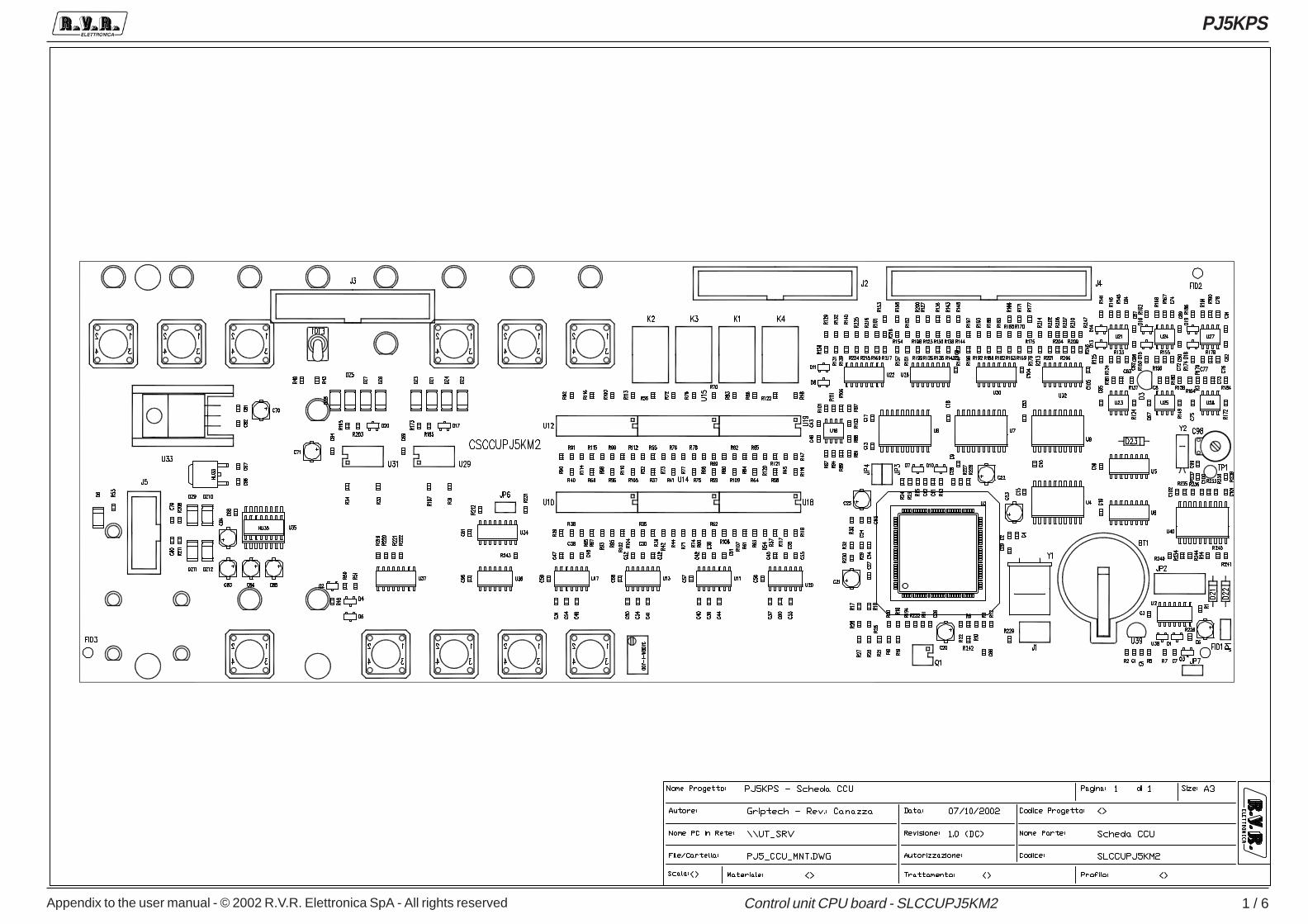
Appendix to the user manual - © 2002 R.V.R. Elettronica SpA - All rights reserved
PJ5KPS
1 / 6Control unit CPU board - SLCCUPJ5KM2
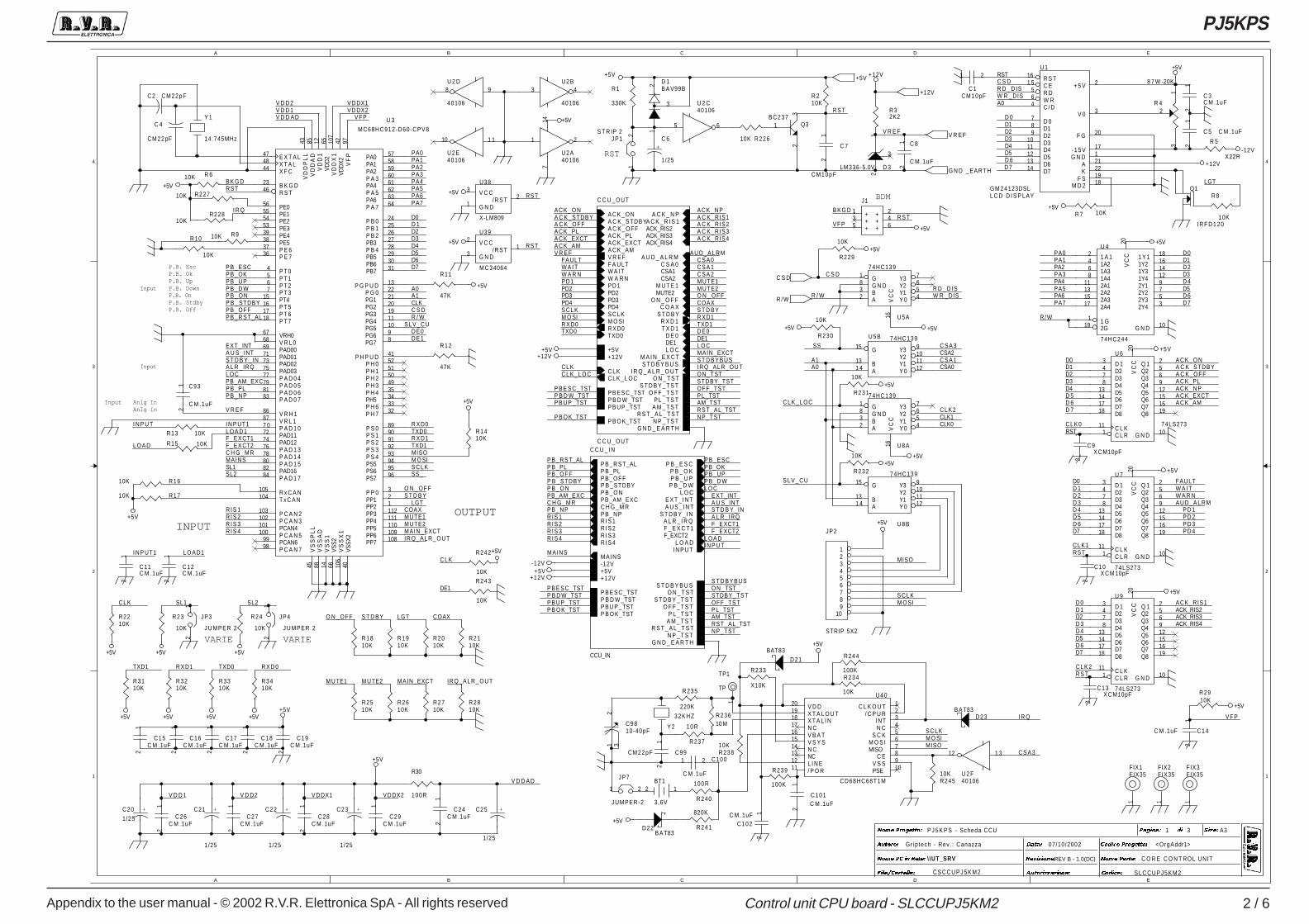
Appendix to the user manual - © 2002 R.V.R. Elettronica SpA - All rights reserved
PJ5KPS
2 / 6Control unit CPU board - SLCCUPJ5KM2
A
A
B
B
C
C
D
D
E
E
4 4
3 3
2 2
1 1
P.B. On
Anlg InAnlg In
P.B. Up
P.B. Esc
P.B. Off
Input
P.B. Stdby
INPUT
Input
P.B. Ok
P.B. Down
OUTPUT
Input
RST
BDM
VARIE VARIE
\ \UT_SRV C O R E C O N T ROL UNIT
SLCCUPJ5KM2
REV B - 1.0(DC)
P J 5 K P S - Scheda CCU
<OrgAddr1>
CSCCUPJ5KM2
Gr ip tech - Rev. : Canazza 07/10/2002
31 A3
� � � � � � � � � � � � �
� � � � � � � � � � � � � � � � � � �
� � � � � � � � � � � �
� � � � � � � � � � � � �
� � � � �
� � � � � � � �
� � � � � �
� � � � � � � � � �
� � � � � � � � � � �
� � � � � � � � � ��
C C U _OUT
C C U _OUT
A C K _ O NA C K_STDBYA C K_OFFA C K _ PLA C K _EXCTA C K _AM
F A ULTW A I TW A R NP D 1PD2PD3PD4
A C K _ N PA C K _ R I S 1ACK_RIS2ACK_RIS3ACK_RIS4
C S A 0CSA1CSA2
M U T E 1MUTE2
O N _ O F FC O A X
S T D B YS C L KM O SIR X D0TXD0
R X D 1T X D 1
D E 0DE1
A U D _ A L R MV R EF
L O C
S T D B Y B U S
+5V+12V
C L KC L K _ L O C O N _ T S T
O F F _ T S TP L _ T S T
A M _ T S TR S T _ A L _ T S T
S T D B Y _ T S T
G N D _ E A R T HP B O K_TST
P B U P _ TSTP B D W _TSTP B E S C _TST
N P _ T S T
M A I N _ E X C T
I R Q _ A L R _ O U T
C C U _ I N
CCU_IN
P B _ R S T_ALP B _PLP B _ O F FP B _STDBYP B _ O NPB_AM_EXCC H G _ M RP B _ N PR I S 1R I S 2R I S 3R I S 4
P B _ E S CP B _ O KP B _ U PP B _ D W
F _ E X C T 1F_EXCT2
E X T _ I N TA U S _ I N T
S T D B Y _ I NA L R _ I R Q
L O C
L O A DI N P U T
MAINS
S T D B Y B U S
+5V+12V
-12V
O N _ T S T
R S T _ A L _ T S T
O F F _ T S TS T D B Y _ T S T
P L _ T S TA M _ T S T
G N D _ E A R T HN P _ T S T
P B E S C _TSTP B D W _TSTP B U P _ TSTP B O K_TST
C H G _ M R
P B _ O F FCLK
B K G D
P B _ R S T_AL
MUTE1
PA2
F_EXCT2
D E 1
P B _STDBY
PB_AM_EXC
PA5
COAX
B K G D
A1
F_EXCT1
V D D1
S C L K
PA1
L O C
V F P
LGT
D E 0
RST
P B _ O N
L O A D 1
PA4
V D D A D
A L R _IRQ
S T D B Y
P B _ D W
M O SI
PA0
I N P UT1
PA3
S T D B Y _ IN
P B _ U P
MAINS
R S T
R / W
P B _OK
PA7
R I S 2
EXT_INT
SS_
P B _ E SC
C S D
R I S 1
P B _PL
PA6
MUTE2
V F P
PA1
R D _ D IS
PA5
C L K 0
PA3PA2
PA6
C S D
PA0
C L K 1
PA7
PA4
A0
D 1
D7
D0
D6
D2
D4D5
D3
D1
D0
D7
D1
D3
D 6
D4
D 6
D3
D 5
D2
D 6
D4
D2
D0
D2D1
D3
D7
D 1
D3
D6
D 2
D0
D 7
D7
D2
D 3
D6
D5
D7
D1
D 5
D5
D4D5
D 4
D4
C L K 2
SS_
C S A 1CSA2
CSA0
CLK2
CLK0CLK1
R / WR D _ D IS
A1
R S T
D0
D 0
LGT
V R EF
RST
SL1
TXD0R X D0
TXD1R X D1
A C K _ O NA C K_STDBYA C K_OFFA C K _PL
A C K _EXCTA C K_AM
FAULTW A I TW A R N
P D 1P D 2P D 3P D 4
ACK_RIS1ACK_RIS2ACK_RIS3ACK_RIS4
I N P UT1 L O A D1
A C K _ O NA C K_STDBYA C K_OFFA C K _ PLA C K _EXCTA C K _AM
FAULTW A I TW A R NP D 1PD2PD3PD4
A C K _ N PA C K_RIS1A C K_RIS2A C K_RIS3A C K_RIS4
C S A 0C S A 1C S A 2MUTE1MUTE2
COAXS T D BYS C L K
M O SIR X D0TXD0
R X D1TXD1D E 0DE1
A0
W R _DIS
R/W
A0
W R _DIS
P B _ E SC
A U D _ A L R M
A U D _ A L R MV R EF
SL2
L O C
R I S 1S T D B Y _IN
L O A D
MAINS
P B _ UP
P B _ N P
EXT_INT
P B _ O F F
R I S 3
PB_AM_EXC
PB_OK
P B _STDBY
P B _ R S T_ALP B _PL
C H G _ M R
P B _ O N
R I S 4
R I S 2
P B _ D W
F_EXCT1A L R_IRQ
L O C
I N P U T
S T D B Y B U S
S T D B Y B U S
V D D A D
O N _ OFF
O N _ OFF
A U S _INT
A U S_INT
C L KC L K _ L O C
C L K
ON_TSTSTDBY_TSTOFF_TSTPL_TSTAM_TSTRST_AL_TST
OFF_TST
RST_AL_TST
STDBY_TST
AM_TST
O N _ TST
PL_TST
MISO
I N P U T
L O A D
O N _OFF
MAIN_EXCTIRQ_ALR_OUT
S T D BY LGT COAX
IRQ_ALR_OUTMAIN_EXCTM U TE1 M U TE2
V D D2 V D DX1
P B _ N P
TXD1 R X D1 R X D 0TXD0
A C K _ N P
R I S 3R I S 4
S L V _ C U
SL2
SL1
NP_TST
P B E S C _TSTP B D W _TSTP B U P _ TSTP B O K_TST
P B D W _TSTP B U P _ TST
P B E S C _TST
P B O K_TST NP_TST
MISO
S C L KM O SI
V R EF
MAIN_EXCT
C S D
C L K _ L O C
S L V _ C U
C S A 3
I R Q
S C L KM O SIMISO
C S A 3
V D D1
RST
V D DX2V D DX1
V D DX2
V D D2
RST
F_EXCT2
I R Q
C L K
DE1
IRQ_ALR_OUT
V F P
RST
RST
RST
+5V+12V
+5V-12V
+12V
+5V
-12V
+5V
+5V
+5V
+5V
+5V
+5V
+5V
+5V
+5V
+12V
+5V
+12V+5V
+5V
+5V
+5V
+5V
+5V
+5V
+5V
+5V
+5V
+5V
+5V
+5V
+5V+5V
+5V
+5V
+5V
+5V
+5V
+5V+5V
+5V
+5V
R1410K
C 4
C M 2 2 pF
C16C M .1uF
12
U5A
74HC139
23
1
4567
8
16
AB
G
Y 0Y1Y2Y3
G N D
VC
C
R3310K
R3210K
C24C M .1uF
12
U39
M C 3 4064
2
31
V C C
G N D/ R S T
U 7
74LS273
3478
13141718
111
256912151619
20
10
D 1D2D3D4D5D6D7D8
C L KC L R
Q 1Q2Q3Q4Q5Q6Q7Q8
VC
C
G N D
Q3BC237
1
23
R22810K
R1
330K
C99CM22pF
12
R 5
X22R
C14C M .1uF
12
U 2 E40106
1 110
C29C M .1uF
12
JP7
JUMPER-2
1 2
R2610K
U 9
74LS273
3478
13141718
111
256912151619
20
10
D 1D2D3D4D5D6D7D8
C L KC L R
Q 1Q2Q3Q4Q5Q6Q7Q8
VC
C
G N D
C102C M .1uF 1
2
R234
10K
R1910K
R235
220K
U 6
74LS273
3478
13141718
111
256912151619
20
10
D 1D2D3D4D5D6D7D8
C L KC L R
Q 1Q2Q3Q4Q5Q6Q7Q8
VC
C
G N D
R239
100K
C28C M .1uF
12
FIX1FIX35
1
C17C M .1uF
12
R2910K
C101C M .1uF
12
R12
47K
C9810-40pF
231
U 3MC68HC912-D60-CPV8
7 0
71
72
69
74
86
67
87
76
7
78
4
15
68
80
73
82
16
84
75
5
105
77
17
79
6
81
18
83
89
104
103
90
102101
91
10099
92
98
93949596
57
39
58
56
59
35
60
55
61
41
62
54
63
52
64
53
38
51
24
50
37
49
34
36
33
25
32
2627
47
28293031
4844
46
4345
8588
12 6514 66
107
4210
640
97
1322212019111098
321112111110109108
23
P A D 1 0
PAD01
PAD11
PAD00
PAD12
V R H 1
VRH0
V R L 1
P A D 1 3
P T 3
P A D 1 4
P T 0
PT4
V R L 0
P A D 1 5
PAD02
PAD16
P T 5
P A D 1 7
PAD03
P T 1
R x C A N
P A D 0 4
P T 6
P A D 0 5
P T 2
P A D 0 6
P T 7
P A D 0 7
P S 0
T x C A N
P C A N 2
P S 1
P C A N 3PCAN4
P S 2
P C A N 5PCAN6
P S 3
P C A N 7
P S 4PS5PS6PS7
PA0
PE4
PA1
PE0
PA2
P H 4
P A 3
PE1
PA4
P H P U D
P A 5
PE2
PA6
P H 0
P A 7
PE3
PE5
P H 1
P B 0
P H 2
P E 6
P H 3
PH5
P E 7
P H 6
P B 1
P H 7
P B 2PB3
E X T A L
P B 4PB5PB6PB7
X T A LX F C
R S T
VD
DP
LL
VS
SP
LL
VD
DA
DV
SS
AD
VD
D1
VDD
2V
SS
1VS
S2V
DD
X1
VDD
X2V
SS
X1
VSSX
2V
FP
P G P U DP G 0PG1PG2PG3PG4PG5PG6PG7
P P 0PP1PP2PP3PP4PP5PP6PP7
B K G D
Y 2
32KHZ
C11C M .1uF
12
C27C M .1uF
12
D21BAT83
C93
C M .1uF
12
R231
10K
R230
10K
R23
10K
R3110K
R2210K
R32K2
R22610K
C9X C M10pF
12
R 4
8 7 W -20K
13
2
R2810K
D 3LM336-5.0V
2
3
1
R23810K
JP3
J U MPER 2
12
R13 10K
C10X C M 10pF
12
U1
G M 2 4 123DSLL C D D I S P LAY
1 55
4
789
1011121314
17
2
3
2122
6
1
16
1918
20
C ER D
C / D
D 0D1D2D3D4D5D6D7
- 1 5 V
+ 5 V
V 0
AK
W R
G N D
R S T
F SM D 2
F G
R243
10K
FIX2FIX35
1
R1610K
+C 6
1/25
R2510K
R242
10K
R237
10R
R30
100R
R11
47K
Y 1
14.745MHz
U 2 D
40106
98
JP2
STRIP 5X2
123456789
10
C18C M .1uF
12
Q1
I R F D 1 20
C 7
CM10pF
12
R24
10K
+C201/25
R 610K
C12C M .1uF
12
D22B A T83
R2010K
+C21
1/25
C 3C M .1uF
12
J1
135
246
+++
+++
+C22
1/25
U 4
74HC244
2468
11131517
119
181614129753
20
10
1 A 11A21A31A42A12A22A32A4
1 G2G
1 Y 11Y21Y31Y42Y12Y22Y32Y4
VC
C
G N D
R8
10K
+C23
1/25
D23B A T83
TP1
TP
1
R241
820K
U8B
74HC139
1 413
15
1211109
AB
G
Y 0Y1Y2Y3
FIX3FIX35
1
U 2 A40106
1 2
147
U 5 B 74HC139
1 413
15
1211109
AB
G
Y 0Y1Y2Y3
R1710K
C 8
C M .1uF
12
C1C M 1 0 pF
1 2
C100
C M .1uF
1 2
R910K
C19C M .1uF
12
BT1
3,6V
12
U 2 B
40106
3 4
R22710K
R7 10K
R2710K
JP4
J U MPER 2
12
C2 CM22pF
C13X C M10pF
12
C15C M .1uF
12
R233
X10KR3410K
D 1B A V99B
1
3
2
R240
100R
R1810K
R15 10K
JP1S T R IP 2
12
R23610 M
R244
100K
U 2 C40106
5 6
R2110K
U 2 F40106
1 312
C 5 C M .1uF
12
C26C M .1uF
12
U8A
74HC139
23
1
4567
8
16
AB
G
Y 0Y1Y2Y3
G N D
VC
C
R 210K
R229
10K
U38
X-LM809
3
12
V C C
G N D/ R S T
R232
10K
+C25
1/25
R10
10K
U40
CD68HC68T1M
12345678910
20191817161514131211
C L K O U T/ C P U R
INTN C
S C KM O S IMISO
C EV S SPSE
V D DX T A L O U TX T A L I NN CV B A TV S Y SN CNCL I N E/ P O R
R24510K
C S D
R/W
+5V
+12V
V R EF
G N D _EARTH
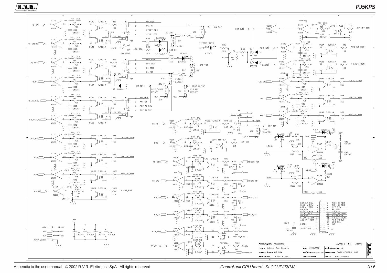
Appendix to the user manual - © 2002 R.V.R. Elettronica SpA - All rights reserved
PJ5KPS
3 / 6Control unit CPU board - SLCCUPJ5KM2
A
A
B
B
C
C
D
D
E
E
4 4
3 3
2 2
1 1
ON
STDBY
LOCAL
REMOTE
OFF
POWERLOWER
ALARMRESET
AUT/MAN ECXT
ESC
OK
RS232
UP
DW
NOM.POWER
INTERLOCK
\ \UT_SRV C O R E C O N T ROL UNIT
SLCCUPJ5KM2
REV B - 1.0 (DC)
PJ55000MC
<>
C S CCUPJ5KM2
Gr ip tec - Rev. : Canazza 07/10/2002
32 A3
� � � � � � � � � � � � �
� � � � � � � � � � � � � � � � � � �
� � � � � � � � � � � �
� � � � � � � � � � � � �
� � � � �
� � � � � � � �
� � � � � �
� � � � � � � � � �
� � � � � � � � � � �
� � � � � � � � � ��
O N _ R EM
STDBY_TST
STDBY_REM
L O C _ SEL
PL_REM
O F F _ R E M
AM_TST
L O C _ SEL
RST_AL_REM
A M _REM
C H G _ M R _ R EM
R I S 3_ IN_REM
R I S 4_ IN_REM
AUS_INT_REM
F_EXCT2_REM
EXT_INT_REM
F_EXCT1_REM
RIS1_ IN_REM
RIS2_ IN_REM
O N _ R EMSTDBY_REM
O F F _ R E MPL_REMA M _REM
N P _ R E MC H G _ M R _ R EM
R I S 2_ IN_REM
R I S 3_ IN_REMR I S 4_ IN_REM
L O C _ SELA L R_ IRQBUSF_EXCT2_REM
L O A D + I N P +
ALR_ IRQBUS
L O A D +
I N P +
L O C _ SEL
L O C _ SEL
L O C _ SEL
OFF_TST
RST_AL_TST
RST_AL_REM
F_EXCT1_REM
PL_TST
O N _ TST
L O C _ SEL
N P _ R EM
R I S 1_ IN_REM
AUS_INT_REM
S T D B Y B U S
MAINS_BUS
MAINS_BUS
EXT_INT_REM
+12V
-12V
-12V
+12V
+5V
+5V
-12V
-12V
+5V
+5V
+12V
+12V
+12V
+12V
+12V
+12V +12V
+5V
+12V
+5V
-12V
+12V
+12V
+12V
+12V
+12V
+12V
+12V
+12V
+12V
+12V
+5V
+5V
+5V
+5V
+5V
+5V
+5V
+5V
+5V
+5V
+5V
+5V
+5V
+5V
+5V
+5V
+5V
+5V
+5V
+5V
+5V
+5V
+5V
+5V
+5V
+5V
+5V
R106 10k
C48C M .1uF
12
C37
C M .1uF
12
C53C M .1uF
12
U11B
40106
34
R118
47K
U15B TLP521-43
4
14
13
U 1 8 C TLP521-45
6
12
11
D11
B A V99B1
3
2
C38C M .1uF
12
R114 2K2
R76
47K
R92
1K5
R43
1K5
R66 2K2
R10110K
U 1 0 D TLP521-47
8
10
9
R53
1K5
+
-
U16A
LM258
3
21
84
R94 33K
U 1 1C
40106
56
R68
1K5
C45C M .1uF
12
S12B3F
13
24
U 1 1F
40106
1 312
S3
S W S P D T
21
3
R89 10k
R120 2K2U18A
TLP521-41
2
16
15
U10B TLP521-43
4
14
13
C46C M .1uF
12
R73 2K2
R81
33K
S5B3F
13
24
DL2
L E D-D5
R37
1K5
R99
47K
U18B TLP521-43
4
14
13
C52C M .1uF
12
U 1 1D
40106
98
C44C M .1uF
12
U14A TLP521-4
1
2
16
15
U19A TLP521-41
2
16
15
R40
1K5
R64
1K5
U 1 7D
40106
98
R86
1K5
U12A
TLP521-41
2
16
15
R107 2K2
C57C M .1uF
12
+
K2
TQ2
89
7
32
41
10
R72
1K5
D 4
B A V99B
1
3
2
R84 2K2
U19B
TLP521-43
4
14
13
U 1 5D TLP521-47
8
10
9
S8B3F
13
24
R80 2K2
R109
1K5
R49
1K5
C54C M .1uF
12
R117 2K2
R45 2K2
U20B
40106
34
U 1 9D TLP521-47
8
10
9
R103 10k
S6
B3F
13
24
R104
47K
R79 1K5
R93 2K2
U10A
TLP521-41
2
16
15
R69
47K
R58
1K5
U15A TLP521-41
2
16
15
U 1 7C
40106
56
R119
1K5
R77 2K2
C32C M .1uF
12
U13A
40106
1214
7
S9
B3F
13
24
R42 2K2
DL4
L E D-D3
C55
C M .1uF
12
R74
47K
J 2
C O N 2 6 A P
13579
1113
2468101214
151719212325
161820222426
+++++++
+++++++
++++++
++++++
R88 10kR87
10K
R41
1K5
C49C M .1uF
12
R67
47K
R65 2K2
D 5
B A V99B
1
3
2
+
K4
TQ2
32
4
89
71
10
R56
1K5
U12B TLP521-43
4
14
13
C34
C M .1uF1
2S4B3F
13
24
C58C M .1uF
12
U 1 2D TLP521-47
8
10
9C47
C M .1uF
12
C56C M .1uF
12
C51CM.47uF
12
R110 2K2
R85
47K
+
-
U16B
LM258
5
67
R82
47K
R38 2K2
R83
1K5
C40
C M .1uF
12
U11E
40106
1 110
U 1 3C
40106
56
R48
1K5
C35C M .1uF
12
C33C M .1uF
12
R78
47K
U 1 2C
TLP521-45
6
12
11
S11B3F
13
24
U14B TLP521-43
4
14
13
C50
C M .1uF
12
U17E
40106
1 110
U20E
40106
1 110
R44
47K
U 2 0D
40106
98
R111 33K
C36
C M .1uF
12
R35 2K2
D 7
B A V99B1
3
2
U 1 0 C TLP521-45
6
12
11
C43C M .1uF
12
U17B
40106
34
DL3
L E D-D5
R105
1K5
+
K1
TQ2
89
7
32
41
10
U20A
40106
12
147
U 2 0F
40106
1 312
U 2 0C
40106
56
C30C M .1uF
12
R98 2K2
R36
47K
R91
47K
U 1 9C TLP521-45
6
12
11
R62
47K
R100
1K5
R47
47K
R39
47K
C59C M .1uF
12
R95
47K
R52 2K2U13B
40106
34
R97
33K
U 1 4D TLP521-47
8
10
9S1B3F
13
24
R54 2K2
C60C M .1uF
12
R63
47K
D 8
B A V99B1
3
2
R75
1K5
R57
47K
R71 2K2
R5110K
R60 2K2
R70
1K5
S7B3F
13
24
R113
1K5
D10
B A V99B1
3
2
R115
47K
C39C M .1uF
12
+
K3
TQ2
32
4
89
71
10
R96
1K5
DL1
L E D-D5
U 1 3D
40106
98
U 1 7F
40106
1 312
C31
C M .1uF
12
R122
2K2
R46
1K5R50
2K2
Q2
B C 2 37
1
23
U 1 3F
40106
1 312
R116
1K5
S2 B3F
13
24
R102 2K2
R59
1K5
R61 2K2
C42C M .1uF
12
U 1 4C TLP521-4
5
6
12
11
U17A
40106
12
147
R112
47K
D 6 1N4004
U 1 8D TLP521-47
8
10
9
U 1 5C TLP521-4
5
6
12
11
S10B3F
13
24
R108
1M
C41C M .1uF
12
U13E
40106
1 110
R55
47K
U11A
40106
12
147
R90 2K2
U 3 6 D
40106
98
R121
47K
P B _ ON
PB_STDBY
PB_PL
P B _ O F F
P B _ R S T_AL
PB_AM_EXC
C H G _ M R
RIS3
RIS4
EXT_INT
R I S 1
A U S_INT
R I S 2
F_EXCT1
F_EXCT2
A L R _IRQ
P B _OK
P B _ E SC
L O C
S T D B Y _ IN
L O AD
I N P UT
S T D B Y B U S
+12V
-12V
+5V
ON_TST
STDBY_TST
OFF_TST
PL_TST
AM_TST RST_AL_TST
G N D_EARTH
P B _ U P
P B _ D W
P B _ N P
P B E S C _TST
P B D W _TST
P B U P _TST
P B OK_TST
NP_TST
MAINS
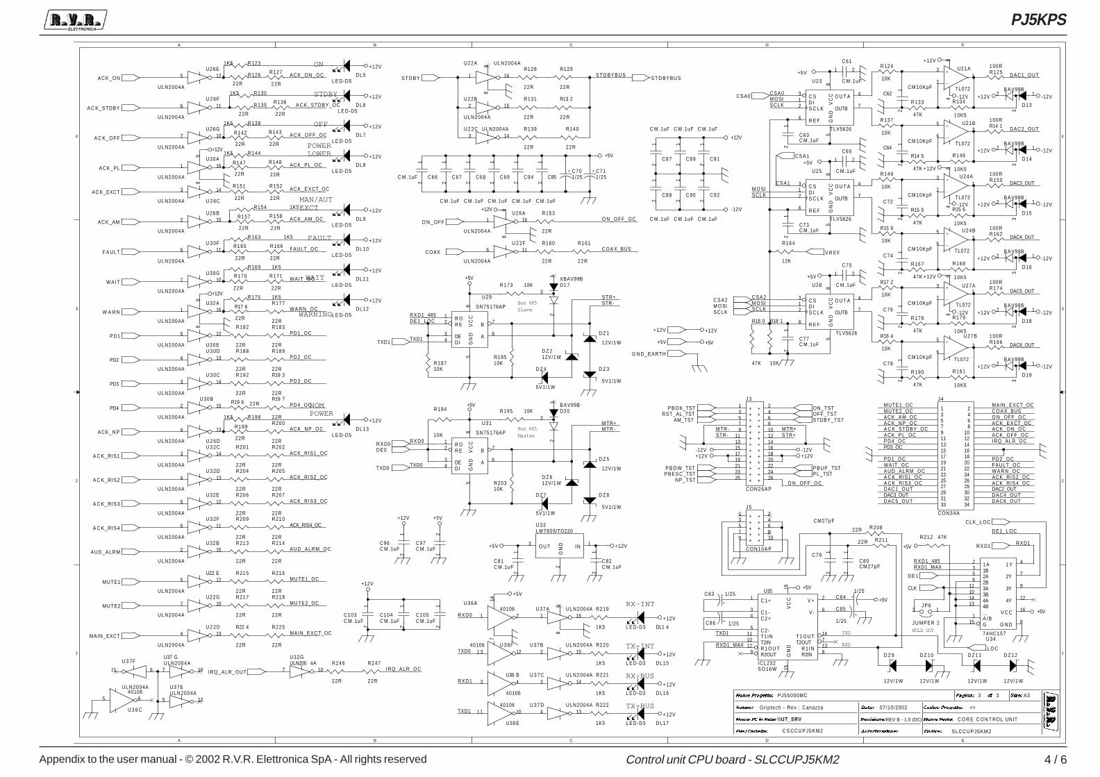
Appendix to the user manual - © 2002 R.V.R. Elettronica SpA - All rights reserved
PJ5KPS
4 / 6Control unit CPU board - SLCCUPJ5KM2
A
A
B
B
C
C
D
D
E
E
4 4
3 3
2 2
1 1
Bus 485Slave
RXD
TXD
RX-INT
TX-INT
TX-BUS
RX-BUS
ON
STDBY
OFF
POWER LOWER
MAN/AUTEXCT
FAULT
WAIT
WARNING
HOLD OUT
NOMPOWER
Bus 485Master
\ \UT_SRV C O R E C O N T ROL UNIT
SLCCUPJ5KM2
REV B - 1.0 (DC)
PJ55000MC
<>
C S CCUPJ5KM2
Gr ip tech - Rev. : Canazza 07/10/2002
33 A3
� � � � � � � � � � � � �
� � � � � � � � � � � � � � � � � � �
� � � � � � � � � � � �
� � � � � � � � � � � � �
� � � � �
� � � � � � � �
� � � � � �
� � � � � � � � � �
� � � � � � � � � � �
� � � � � � � � � ��
A C K _ O N _ O C
A C K_STDBY_OC
A C K _ O F F _ O C
ACK_PL_OC
A C K _ E X CT_OC
A C K _ A M_OC
FAULT_OC
DAC1_OUT
MUTE1_OC
S T D B Y B U S
O N _ O F F _ O C
C O A X_BUS
STR+
TXD1
R X D 1 _485
STR-
DAC2_OUT
DAC4_OUT
DAC3_OUT
DAC5_OUT
DAC6_OUT
C S A 2
S C L K
S C L K
C S A 0
M O SI
S C L KM O SI
M O SI
A U D _ A L R M _ O C
ACK_RIS2_OC
P D 2 _ O C
P D 4 _ O C
A C K _ N P _ O C
P D 1 _ O C
P D 3 _ O C
ACK_RIS1_OC
W A R N _ O C
W A I T _ O C
TXD0
R X D 1
TXD1
R X D 0
TXD1
RXD1_MAX
R X D1
R X D 1 _485RXD1_MAX
C S A 1
D E 1 _ L O C
D E 1 _ L O C
ACK_RIS3_OC
ACK_RIS4_OC
MTR+MTR-
R X D0
TXD0
MTR-STR-
O N _ O F F _ O C
STR+MTR+
A C K _ N P _ O CA C K _ A M_OC
ACK_PL_OC
MUTE2_OCMUTE1_OC
A C K_STDBY_OC
P D 4 _ O CPD3_OC
W A I T _ O CP D 1 _ O C
A U D _ A L R M _ O C
DAC5_OUTDAC3_OUT
A C K_RIS3_OCA C K_RIS1_OC
DAC1_OUT
MAIN_EXCT_OCC O A X_BUS
ACK_RIS4_OC
A C K _ O N _ O CA C K _ E X CT_OC
DAC4_OUT
O N _ O F F _ O C
ACK_RIS2_OC
DAC6_OUT
DAC2_OUT
P D 2 _ O C
MUTE2_OC
MAIN_EXCT_OC
W A R N _ O CFAULT_OC
A C K _ O F F _ O C
IRQ _ A L R _ O C
IRQ_ALR_OC
+12V
+12V
+12V
+12V
+12V
+12V
+12V
+12V
+12V
+12V
+12V
+12V
+12V
+12V
+12V
+12V
+5V
+5V
+5V
+12V
+12V
+12V
+12V
+12V
+12V
-12V
-12V
-12V
-12V
-12V
-12V
-12V
-12V
-12V
+5V
+5V
+5V
+5V
+5V
+12V
+5V
+5V
+5V
+5V
+12V-12V
+12V+5V
-12V+12V
+12V
-12V
+12V +5V
+12V
+12V
+12V
+12V
R160
22R
R173 10K
R143
22R
R22 4
22R
R18 0
47K
R221
1K5
U22A ULN2004A
1 16
89
U31
SN75176AP
12
34
7
6
58
R OR E
DEDI
B
A
GN
DV
CC
R1231K5
R186100R
U36E
401061 1 10
DL16L E D-D3
U26E
ULN2004A
5 12
R171
22R
R14 1100R
R20310K
U30A
ULN2004A
1 16
89
R191
10K5
R18710K
R162100R
U26B
ULN2004A
2 15
U 3 0D
ULN2004A
4 13
C68
C M .1uF
12
+
-
U21B
TL072
5
67
R168
10K5
R205
22R
DL8L E D-D5
C87
C M .1uF
12
D Z 1 1
12V/1 W
R148
22R
R19 7
22R
R1381K5
U 2 2D
ULN2004A
4 13
U37A ULN2004A1 16
89
U 2 2C ULN2004A3 14
+
-
U27B
TL072
5
67
R212 47K
C72C M 1 0 K pF1
2
R220
1K5
DL7L E D-D5
R154 1K5
R151
22R
R17 2
10K
DL9L E D-D5
DL10L E D-D5
R177
22R
R219
1K5
C90
C M .1uF
12
C96C M .1uF
12
D Z 1
12V/1 W
R214
22R
R169 1K5
U 2 6F
ULN2004A
6 11 DL6L E D-D5
R225
22R
D18
B A V99B1
3
2
R209
22R
C62C M 1 0 K pF1
2
U 3 7D ULN2004A4 13
U32B
ULN2004A
2 15
D Z 3
5V1/1 W
R133
47K
U 3 0F
ULN2004A
6 11
J 3
C O N 2 6 A P
13579
1113
2468101214
151719212325
161820222426
+++++++
+++++++
++++++
++++++
U 3 6 C
401065 6
+
-
U24B
TL072
5
67
R215
22R
R15 6
10K5
U32E
ULN2004A
5 12
C104C M .1uF
12
C105C M .1uF
12
R157
22R
U 3 6F401061 3 12
C66C M .1uF
12
R216
22R
R129
22R
D Z 612V/1 W
R146
10K5R149
10K
D Z 7
5V1/1 W
C69
C M .1uF
12
U26A
ULN2004A
1 16
89
DL13L E D-D5
R127
22R U23
TLV5626
312
6
4
7
85
C SDIS C L K
R E F
O U T A
OUTB
VC
CG
ND
D Z 5
12V/1 W
D Z 8
5V1/1 W
C76C M 1 0 K pF1
2
U25
TLV5626
312
6
4
7
85
C SDIS C L K
R E F
O U T A
OUTB
VC
CG
ND
R222
1K5
R125100R
+ C701/25
R134
10K5R137
10KC63C M .1uF
12
R195 10K
D19
B A V99B1
3
2
R182
22R
U37 GULN2004A
7 10
U 3 0C
ULN2004A
3 14
U 2 6DULN2004A
4 13
C88
C M .1uF
12
U3474HC157
2356
11101413
115
4
7
9
12
16
8
1 A1B2A2B3A3B4A4B
A / BG
1 Y
2Y
3Y
4Y
V C C
G N D
R152
22R
D Z 9
12V/1 W
R153
22R
U29
SN75176AP
12
34
7
6
58
R OR E
DEDI
B
A
GN
DV
CC
R247
22R
R18 4
10K
U 2 2F
ULN2004A
6 11
R206
22R
D Z 4
5V1/1 W
R207
22R
R124
10K
C61
C M .1uF
1 2
R175 1K5
U33LM7805/TO220
2
13
GN
D I NO U T
R135
22R
U28
TLV5626
312
6
4
7
85
C SDIS C L K
R E F
O U T A
OUTB
VC
CG
ND
C91
C M .1uF
12
D15
B A V99B1
3
2
R188
22R
C95
C M .1uF
12
U32GULN200 4A
7 10
R139
22R
U 3 2D
ULN2004A
4 13
U 3 7F
ULN2004A
611
R199
22R
DL1 4L E D-D3
C97C M .1uF
12
U26G
ULN2004A
7 10
R158
22R R15 9
10K
U37B ULN2004A2 15
U22B
ULN2004A
2 15
R1981K5
R218
22R
C94
C M .1uF
12
R164
12K
R190
47K
C73C M .1uF
12
R126
22R
R165
22R
R14 5
47K
R167
47K
R163 1K5
R217
22R
R161
22R
R15 5
47K
DL15L E D-D3
D13
B A V99B1
3
2
+
C83 1/25
R140
22R
U36 B
40106
3 4
+
C86 1/25
+C841/25
R1441K5
R192
22R
+
-
U21A
TL072
3
21
84
R179
10K5R183
22R
U 2 6CULN2004A
3 14
C80CM27pF
12
R201
22R
U22 E
ULN2004A
5 12
+C85
1/25
D20B A V99B
1
3
2
R20822R
+
-
U27A
TL072
3
21
84
R21122R
U35
ICL232S O 16W
1
34
5111012
9
2
6
147138
1615
C 1 +
C 1 -C 2 +
C 2 -T 1 I NT2INR 1 O U TR2OUT
V +
V-
T 1 O U TT2OUT
R 1 I NR2IN
VC
CG
ND
R142
22RC65
C M .1uF
1 2
DL11L E D-D5
C82C M .1uF
12
R18510K
DL5L E D-D5
D17XBAV99B
1
3
2
DL12L E D-D5
R170
22R
R13 2
22R
C64C M 1 0 K pF1
2
R150100R
U30EULN2004A
5 12
U30G
ULN2004A
7 10
DL17L E D-D3
R136
22R
R18 1
10K
U 3 2F
ULN2004A
6 11
C79
CM27pF
12
J 5
C O N 1 0 A P
13579
246810
+++++
+++++
R189
22R
U32A
ULN2004A
1 16
89
D14
B A V99B1
3
2
C77C M .1uF
12
U22G
ULN2004A
7 10
C92
C M .1uF
12
JP6
J U MPER 2
12
+
-
U24A
TL072
3
21
84
R174100R
R200
22R
R204
22R
R147
22R
R19 6 22R
C67
C M .1uF
12
C103C M .1uF
12
U36A40106
1 2
147
R246
22RU37EULN2004A
5 12
C74C M 1 0 K pF1
2
R210
22R
C89
C M .1uF
12
D Z 12
12V/1 W
R1301K5
R128
22R
R17 6
22R
+ C711/25
R166
22R
R194
10K
D16
B A V99B1
3
2
U 3 7C ULN2004A3 14
J 4
C O N 3 4 A
13579111315171921232527293133
2468
10121416182022242628303234
D Z 212V/1 W
U30B
ULN2004A
2 15
D Z 10
12V/1 W
C75
C M .1uF
1 2
R131
22R
R19 3
22R
R213
22R
U 3 2C
ULN2004A
3 14
C81C M .1uF
12
C78C M 1 0 K pF1
2
R178
47K
R202
22R
A C K _ O N
A C K_STDBY
A C K_OFF
A C K _ PL
A C K _EXCT
A C K _AM
F A ULT
W A I T
W A R N
P D 1
PD2
PD3
PD4
A C K _ N P
A C K_RIS1
A C K_RIS2
A U D _ A L R M
MUTE1
MUTE2
R X D1
TXD1
S T D BY
O N _OFF
COAX V R EF
M O SIS C L K
C S A 2
C S A 0
C S A 1
L O C
+12V
+5V
D E 1
CLK
C L K _ L O C
G N D_EARTH
A C K_RIS3
A C K_RIS4
R X D0
TXD0
D E 0
NP_TST
ON_TST
P B E S C _TSTP B U P _ TST
STDBY_TST
P B O K_TST
PL_TST
OFF_TSTAM_TST
P B D W _TST
RST_AL_TST
S T D B Y B U S
MAIN_EXCT
IRQ_ALR_OUT

Appendix to the user manual - © 2002 R.V.R. Elettronica SpA - All rights reserved
PJ5KPS
5 / 6Control unit CPU board - SLCCUPJ5KM2
CSCCUPJ5KM2 Bill Of Materials Page1
Item Q.ty Reference Part_____________________________________________________________________________________________
1 1 BT1 3,6V2 2 C7,C1 CM10pF3 3 C2,C4,C99 CM22pF4 75 C3,C5,C8,C11,C12,C14,C15, CM.1uF
C16,C17,C18,C19,C24,C26,C27,C28,C29,C30,C31,C32,C33,C34,C35,C36,C37,C38,C39,C40,C41,C42,C43,C44,C45,C46,C47,C48,C49,C50,C52,C53,C54,C55,C56,C57,C58,C59,C60,C61,C63,C65,C66,C67,C68,C69,C73,C75,C77,C81,C82,C87,C88,C89,C90,C91,C92,C93,C94,C95,C96,C97,C100,C101,C102,C103,C104,C105
5 12 C6,C20,C21,C22,C23,C25, 1/25C70,C71,C83,C84,C85,C86
6 3 C9,C10,C13 XCM10pF7 1 C51 CM.47uF8 6 C62,C64,C72,C74,C76,C78 CM10KpF9 2 C80,C79 CM27pF10 1 C98 10-40pF11 12 DL1,DL2,DL3,DL5,DL6,DL7, LED-D5
DL8,DL9,DL10,DL11,DL12,DL13
12 5 DL4,DL14,DL15,DL16,DL17 LED-D313 8 DZ1,DZ2,DZ5,DZ6,DZ9,DZ10, 12V/1W
DZ11,DZ1214 4 DZ3,DZ4,DZ7,DZ8 5V1/1W15 14 D1,D4,D5,D7,D8,D10,D11, BAV99B
D13,D14,D15,D16,D18,D19,D20
16 1 D3 LM336-5.0V17 1 D6 1N400418 1 D17 XBAV99B19 3 D21,D22,D23 BAT8320 3 FIX1,FIX2,FIX3 FIX3521 1 JP1 STRIP 222 1 JP2 STRIP 5X223 3 JP3,JP4,JP6 JUMPER 224 1 JP7 JUMPER-225 1 J1 BDM26 2 J3,J2 CON26AP27 1 J4 CON34A28 1 J5 CON10AP29 4 K1,K2,K3,K4 TQ230 1 Q1 IRFD12031 2 Q3,Q2 BC23732 1 R1 330K
33 59 R2,R6,R7,R8,R9,R10,R13, 10KR14,R15,R16,R17,R18,R19,R20,R21,R22,R23,R24,R25,R26,R27,R28,R29,R31,R32,R33,R34,R51,R87,R88,R89,R101,R103,R106,R124,R137,R149,R159,R172,R173,R181,R184,R185,R187,R194,R195,R203,R226,R227,R228,R229,R230,R231,R232,R234,R238,R242,R243,R245
34 27 R3,R35,R38,R42,R45,R50, 2K2R52,R54,R60,R61,R65,R66,R71,R73,R77,R80,R84,R90,R93,R98,R102,R107,R110,R114,R117,R120,R122
35 1 R4 87W-20K36 1 R5 X22R37 33 R11,R12,R36,R39,R44,R47, 47K
R55,R57,R62,R63,R67,R69,R74,R76,R78,R82,R85,R91,R95,R99,R104,R112,R115,R118,R121,R133,R145,R155,R167,R178,R180,R190,R212
38 8 R30,R125,R141,R150,R162, 100RR174,R186,R240
39 40 R37,R40,R41,R43,R46,R48, 1K5R49,R53,R56,R58,R59,R64,R68,R70,R72,R75,R79,R83,R86,R92,R96,R100,R105,R109,R113,R116,R119,R123,R130,R138,R144,R154,R163,R169,R175,R198,R219,R220,R221,R222
40 4 R81,R94,R97,R111 33K41 1 R108 1M42 57 R126,R127,R128,R129,R131, 22R
R132,R135,R136,R139,R140,R142,R143,R147,R148,R151,R152,R153,R157,R158,R160,R161,R165,R166,R170,R171,R176,R177,R182,R183,R188,R189,R192,R193,R196,R197,R199,R200,R201,R202,R204,R205,R206,R207,R208,R209,R210,R211,R213,R214,R215,R216,R217,R218,R224,R225,R246,R247
43 6 R134,R146,R156,R168,R179, 10K5R191
44 1 R164 12K45 1 R233 X10K46 1 R235 220K47 1 R236 10M48 1 R237 10R49 2 R239,R244 100K

Appendix to the user manual - © 2002 R.V.R. Elettronica SpA - All rights reserved
PJ5KPS
6 / 6Control unit CPU board - SLCCUPJ5KM2
50 1 R241 820K51 11 S1,S2,S4,S5,S6,S7,S8,S9, B3F
S10,S11,S1252 1 S3 SW SPDT53 1 TP1 TP54 1 U1 GM24123DSL55 6 U2,U11,U13,U17,U20,U36 4010656 1 U3 MC68HC912-D60-CPV857 1 U4 74HC24458 2 U5,U8 74HC13959 3 U6,U7,U9 74LS27360 6 U10,U12,U14,U15,U18,U19 TLP521-461 1 U16 LM25862 3 U21,U24,U27 TL07263 5 U22,U26,U30,U32,U37 ULN2004A64 3 U23,U25,U28 TLV562665 2 U31,U29 SN75176AP66 1 U33 LM7805/TO22067 1 U34 74HC15768 1 U35 ICL23269 1 U38 X-LM80970 1 U39 MC3406471 1 U40 CD68HC68T1M72 1 Y1 14.745MHz73 1 Y2 32KHZ
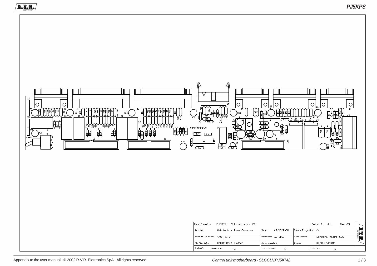
Appendix to the user manual - © 2002 R.V.R. Elettronica SpA - All rights reserved
PJ5KPS
1 / 3Control unit motherboard - SLCCU1PJ5KM2
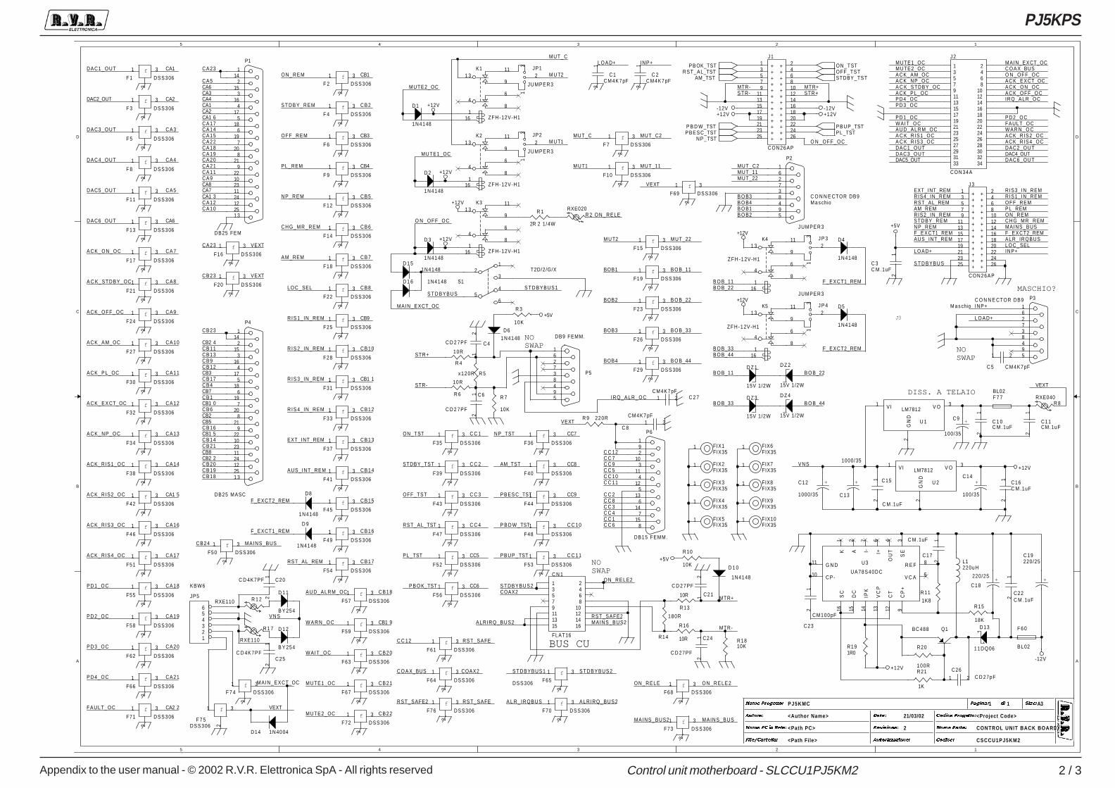
Appendix to the user manual - © 2002 R.V.R. Elettronica SpA - All rights reserved
PJ5KPS
2 / 3Control unit motherboard - SLCCU1PJ5KM2
5
5
4
4
3
3
2
2
1
1
D D
C C
B B
A A
BUS CU
MASCHIO?
DISS. A TELAIO
NOSWAP
NOSWAP
NOSWAP
J3
PJ5KMC
<Project Code>
1
<Author Name>
CONTROL UNIT BACK BOARD
CSCCU1PJ5KM2
<Path PC>
<Path File>
21/03/02
A31
2
� � � � � � � � � � � � �
� � � � � � � � � � � � � � � � � � �
� � � � � � � � � � � �
� � � � � � � � � � � � �
� � � � �
� � � � � � � �
� � � � � �
� � � � � � � � � �
� � � � � � � � � � �
� � � � � � � � � ��
W A R N _ O C
MUTE1_OC
A U D _ A L R M _ OC
C B 7
CB1 1
C B 1 7
C B 1 4
C B 2 1
C B 6
CB9
CB1
CB4
CB3
CB1 9
C B 1 8
C B 1 5
C B 1 3
C B 1 2
C B 1 6
C B 2
VEXT
S T D B Y _ R E M
R I S 4_ IN_REM
C H G _ M R _ R EM
R I S 3_ IN_REM
O F F _ R E M
PL_REM
A M _REM
O N _ R E M
R I S 1_ IN_REM
AUS_INT_REM
RST_AL_REM
F_EXCT2_REM
L O A D+
INP+
EXT_INT_REM
M U T2
MUTE1_OC
MUT_C
M U T1
MAINS_BUS2
MTR+
RST_SAFE2
COAX2
C A 9
CA1
CA6
A C K _ O N _ O C
DAC1_OUT
C A 2 1
C A 7
CA2
CA1 5
DAC6_OUT
DAC2_OUT
A C K _ O F F _ O C
ACK_RIS2_OC
P D 4 _ O C
MTR-
STR+
STR-
V N S
VEXT
NP_TST
STDBY_TST
PL_TST
AM_TST
P B E S C _TST
P B O K_TST
P B D W _TST
C A 2 3
C A 2 3
C A 5CA6CA3CA4CA1CA2CA1 6C A 1 7C A 1 4C A 1 5C A 2 2C A 1 8C A 1 9C A 2 0C A 2 1C A 1 1C A 9CA8CA7CA1 3C A 1 2C A 1 0
C B 9
CB1 5
C B 2 3
C B 6
CB7
CB8
CB1 0
C B 1 2
C B 1 3
C B 1 4
C B 2 0
C B 4
CB3
CB2CB5
CB2 2
C B 1 9
C B 1 1
C B 1
CB2 4
C B 1 7
RST_SAFEC C 12
MAINS_BUSMAINS_BUS2
O N _ O F F _ O CO N _ R E LE
MUTE2_OC
MUT_C MUT_C2
MUT_C2MUT_11MUT_22
B O B_11B O B_22
B O B2B O B1B O B4B O B3
F_EXCT1_REM
F_EXCT1_REM
B O B_44F_EXCT2_REMB O B_33
B O B_22B O B_11
B O B_44B O B_33
VEXT
P B U P _ TST
C C 2
CC5
CC6
CC7
CC8
CC9
C C 10
C C 11
C C 12C C 7C C 9C C 5C C 10C C 11
C C 2C C 8C C 3C C 4
C A 1 2
C B 2 2MUTE2_OC
M U T1
FAULT_OC
ACK_RIS3_OC
C O A X_BUS
C A 4
B O B_33BOB3
B O B_22
ACK_RIS4_OC
C A 8
O N _ R E L E
MUT_11
DAC3_OUT
COAX2
C B 2 3
A C K _ P L _OC
W A I T _ O C
C C 4
B O B_44
P D 2 _ O C
BOB2
C A 1 4
A C K _ E X CT_OC
S T DBYBUS2
ALRIRQ_BUS2
C C 1
P D 1 _ O C
L O C _ SEL
B O B_11BOB1
RST_AL_TST
C A 1 1
C B 2 0
MUT_22
ALRIRQ_BUS2
ON_TST
C A 1 9
C A 1 6
C A 1 7
C A 1 0
S T DBYBUS1
A C K _ N P _ O C
S T DBYBUS2
BOB4
C A 2 0
DAC5_OUT
OFF_TST
R I S 2_ IN_REM
C A 1 3
N P _ R E M
C A 3
CA2 2
O N _ R E L E2
M U T2
P D 3 _ O C
A C K_STDBY_OCC B 8
O N _ R E L E 2
C C 3
DAC4_OUT
ACK_RIS1_OC
C A 5
A C K _ A M_OC
C B 5
VEXT
A L R_ IRQBUS
C A 1 8
C B 1 0
INP+
C C 1
L O A D+
C B 2 4 MAINS_BUS
C B 1 8
S T D BYBUS1S T D B Y B U S
V N S
MAIN_EXCT_OC
VEXT
VEXT
C B 2 1
C B 1 6
C C 6
RST_SAFE2 RST_SAFE
O N _ O F F _ O C
S T R-MTR+MTR-STR+
P D 2 _ O C
A C K _ A M_OCC O A X_BUS
P D 1 _ O C
A C K_RIS3_OCDAC2_OUTDAC4_OUT
MUTE1_OC
A C K _ N P _ O C
MAIN_EXCT_OC
DAC3_OUT
A C K _ E X CT_OC
MUTE2_OC
W A I T _ O C
A C K _ O F F _ O C
DAC1_OUT
DAC5_OUT
A C K _ O N _ O C
DAC6_OUT
P D 3 _ O C
FAULT_OC
A C K_RIS1_OCW A R N _ O CACK_RIS2_OC
P D 4 _ O C
A U D _ A L R M _ O C
ACK_PL_OC
ACK_RIS4_OC
O N _ O F F _ O C
A C K_STDBY_OC
RIS1_ IN_REM
ALR_ IRQBUS
STDBY_REMMAINS_BUS
F_EXCT1_REMN P _ R EM
L O C _ SEL
RST_AL_REMAM_REM
RIS4_ IN_REM
S T D B Y B U S
L O A D+
PL_REM
RIS3_ IN_REM
AUS_INT_REM
O N _ R EM
INP+
RIS2_ IN_REM
OFF_REM
EXT_INT_REM
F_EXCT2_REM
C H G _ M R _ R EM
MAIN_EXCT_OC
IRQ_ALR_OC
IRQ _ A L R _ O C
+12V
+5V
+5V
-12V
+12V
+12V
+12V
+12V
+12V
+12V
+12V-12V+12V
-12V
+5V
+12V
C 1 0C M .1uF
12
+C12
1000/35
f
F16 D S S 3 06
1 3
2
f
F56 D S S 3 06
1 3
2
C 3C M .1uF
12
C25C D 4K7PF
12
D Z 1
15V 1/2W
U 1
LM78121
2
3V I
GN
D
V O
C1C M 4 K 7 pF
12
C21
C D 2 7PF
12
fF14 D S S 3 06
1 3
2
f
F32 D S S 3 06
1 3
2
f
F51 D S S 3 06
1 3
2
fF68 D S S 306
1 32
f
F 7 5D S S 3 06
1 3
2
R16
10R
f
F39 D S S 3 06
1 3
2
+
C19220/25
U 2
LM78121
2
3V I
GN
D
V O
D Z 3
15V 1/2W
R10
10K
C4C D 2 7PF
12
D8
1N4148
f
F61 D S S 3 06
1 3
2
R1810K
f
F42 D S S 3 06
1 3
2
fF45 D S S 3 06
1 3
2
fF 6 D S S 3 06
1 3
2
K2
Z F H - 12V-H1
1 311
9
46
81
16
fF49 D S S 3 06
1 3
2
C N 1
FLAT16
13579111315
2468
10121416
f
F66 D S S 3 06
1 3
2
f
F15 D S S 306
1 3
2
P6
DB15 FEMM.
815
714
613
512
411
310
291
R 9 220R
C 8
C M 4 K 7 pF1 2
C 5 C M 4 K 7 pF
1 2
f
F40 D S S 3 06
1 3
2
R13
10R
+
C13
1000/35
f
F 3 D S S 3 06
1 3
2
f
F26 D S S 306
1 3
2
f
F11 D S S 3 06
1 3
2
P1
DB25 FEM
1 325122411231022
921
820
719
618
517
416
315
214
1
D Z 2
15V 1/2W
P2
C O N N E CTOR DB9M a s chio
594837261
Q1BC488
FIX2FIX35
1
D 2
1N4148
K1
Z F H - 12V-H1
1 311
9
46
81
16
P4
DB25 MASC
1 325122411231022
921
820
719
618
517
416
315
214
1
J 1
C O N 2 6 A P
13579
1113
2468101214
151719212325
161820222426
+++++++
+++++++
++++++
++++++
D 3
1N4148
+C14
100/35
f
F50 D S S 306
1 3
2
D 9
1N4148
D Z 4
15V 1/2W
fF 4 D S S 3 06
1 3
2
D 1 0
1N4148
fF72 D S S 3 06
1 3
2
S1
T2D/2/G/X21
3
54
6
K3
Z F H - 12V-H1
1 311
9
46
81
16
fF33 D S S 3 06
1 3
2
fF54 D S S 3 06
1 3
2
f
F34 D S S 3 06
1 3
2
f
F65D S S 3 06
1 3
2
D 1 6 1N4148
R 3
10K
R 8RXE040
K5
Z F H - 1 2V-H1
1 311
9
46
81
16
fF 7 4 D S S 3 06
1 3
2
R 5x 1 2 0R
fF12 D S S 3 06
1 3
2
R14
180R
f
F71 D S S 3 06
1 3
2
C 2C M 4 K 7 pF
12
J 3
C O N 2 6 A P
13579
1113
2468101214
151719212325
161820222426
+++++++
+++++++
++++++
++++++
FIX8FIX35
1
f
F43 D S S 3 06
1 3
2
f
F76 D S S 3 06
1 3
2
f
F47 D S S 3 06
1 3
2
P5
DB9 FEMM.
594837261
R 1 2RXE110
F 7 7BL02
C15
C M .1uF
12
F IX3FIX35
1
U3
UA78S40DC
91213141516
346721
8
510
11
CP
+
CT
VC
P
IPK
DC
SC
SE
OU
TI+I-AK
R E F
V C AC P -
G N D
FIX1FIX35
1
C23
CM100pF
12
C20C D 4K7PF
12
f
F23 D S S 306
1 3
2
D 1 51N4148
R191R0
C6
C D 2 7PF
12
f
F55 D S S 3 06
1 3
2
f
F 8 D S S 3 06
1 3
2
R20
100RR21
1K
f
F21 D S S 3 06
1 3
2
R11
1K8
fF41 D S S 3 06
1 3
2
C 2 7C M 4 K 7 pF
1 2
FIX7FIX35
1
C17
C M .1uF 12
f
F24 D S S 3 06
1 3
2
L1220uH
C11CM.1uF
12
fF59 D S S 3 06
1 3
2
f
F44 D S S 3 06
1 3
2
f
F62 D S S 3 06
1 3
2
JP5
KBW6
123456
+C18
220/25
D4
1N4148
f
F48 D S S 3 06
1 3
2
f
F46 D S S 3 06
1 3
2
D 1 1
B Y 254R15
18K
K4
Z F H - 1 2V-H1
1 311
9
46
81
16
fF37 D S S 3 06
1 3
2
f
F64 D S S 3 06
1 3
2FIX6FIX35
1
fF63 D S S 3 06
1 3
2
JP1
JUMPER3
13
2
fF10 D S S 306
1 3
2
R 4
10R
f
F17 D S S 3 06
1 3
2
FIX4FIX35
1
f
F38 D S S 3 06
1 3
2
R 2RXE020
fF25 D S S 3 06
1 3
2
fF28 D S S 3 06
1 3
2
J P 4
JUMPER3
13
2
f
F52 D S S 3 06
1 3
2
fF57 D S S 3 06
1 3
2
f
F27 D S S 3 06
1 3
2 f
F29 D S S 306
1 3
2
C24
C D 27PF
12
F IX10FIX35
1
+C9
100/35
fF67 D S S 3 06
1 3
2
f
F35 D S S 3 06
1 3
2
C26C D 27pF1 2
F 6 0
BL02
fF 7 D S S 306
1 3
2
D61N4148
D13
1 1 D Q 06
f
F 5 D S S 3 06
1 3
2
C22C M .1uF
12
D5
1N4148
f
F 1 D S S 3 06
1 3
2
C16C M .1uF
12
D14 1N4004
D 1 2
B Y 254
f
F53 D S S 3 06
1 3
2
R 6
10R
fF 2 D S S 3 06
1 3
2
FIX5FIX35
1
f
F30 D S S 3 06
1 3
2
f
F20 D S S 3 06
1 3
2
fF 9 D S S 3 06
1 3
2
R 7
10K
R 1
2R 2 1 /4W
fF73 D S S 306
1 3
2
f
F36 D S S 3 06
1 3
2
f
F70 D S S 306
1 3
2
J P 3
JUMPER3
13
2
D1
1N4148
f
F19 D S S 306
1 3
2
P3C O N N E CTOR DB9M a s chio
594837261
f
F69 D S S 3 06
1 3
2
fF31 D S S 3 06
1 3
2
f
F13 D S S 3 06
1 3
2
FIX9FIX35
1
R 1 7
RXE110
J 2
C O N 3 4 A
13579111315171921232527293133
2468
10121416182022242628303234
fF22 D S S 3 06
1 3
2
f
F58 D S S 3 06
1 3
2
JP2
JUMPER3
13
2
fF18 D S S 3 06
1 3
2
RST_AL_TST
P B D W _TSTP B E S C_TST
STDBY_TST
P B U P _TST
P B OK_TSTOFF_TST
PL_TST
ON_TST
N P _ TST
AM_TST

Appendix to the user manual - © 2002 R.V.R. Elettronica SpA - All rights reserved
PJ5KPS
3 / 3Control unit motherboard - SLCCU1PJ5KM2
SLCCU1PJ5KM2 Bill Of Materials Page1
Item Q.ty Reference Part____________________________________________________________________________________________
1 1 CN1 FLAT162 5 C1,C2,C5,C8,C27 CM4K7pF3 7 C3,C10,C11,C15,C16,C17, CM.1uF
C224 5 C4,C6,C21,C24,C26 CD27pF5 2 C14,C9 100/356 2 C12,C13 1000/357 2 C19,C18 220/258 2 C25,C20 CD4K7PF9 1 C23 CM100pF10 4 DZ1,DZ2,DZ3,DZ4 15V 1/2W11 11 D1,D2,D3,D4,D5,D6,D8,D9, 1N4148
D10,D15,D1612 2 D11,D12 BY25413 1 D13 11DQ0614 1 D14 1N400415 10 FIX1,FIX2,FIX3,FIX4,FIX5, FIX35
FIX6,FIX7,FIX8,FIX9,FIX10
16 75 F1,F2,F3,F4,F5,F6,F7,F8, DSS306F9,F10,F11,F12,F13,F14,F15,F16,F17,F18,F19,F20,F21,F22,F23,F24,F25,F26,F27,F28,F29,F30,F31,F32,F33,F34,F35,F36,F37,F38,F39,F40,F41,F42,F43,F44,F45,F46,F47,F48,F49,F50,F51,F52,F53,F54,F55,F56,F57,F58,F59,F61,F62,F63,F64,F65,F66,F67,F68,F69,F70,F71,F72,F73,F74,F75,F76
17 2 F77,F60 BL0218 4 JP1,JP2,JP3,JP4 JUMPER319 1 JP5 KBW620 2 J1,J3 CON26AP21 1 J2 CON34A22 5 K1,K2,K3,K4,K5 ZFH-12V-H123 1 L1 220uH24 1 P1 DB25 FEM25 2 P2,P3 CONNECTOR DB926 1 P4 DB25 MASC27 1 P5 DB9 FEMM.28 1 P6 DB15 FEMM.29 1 Q1 BC48830 1 R1 2R2 1/4W31 1 R2 RXE02032 4 R3,R7,R10,R18 10K33 4 R4,R6,R13,R16 10R34 1 R5 x120R35 1 R8 RXE04036 1 R9 220R37 1 R11 1K838 2 R12,R17 RXE110
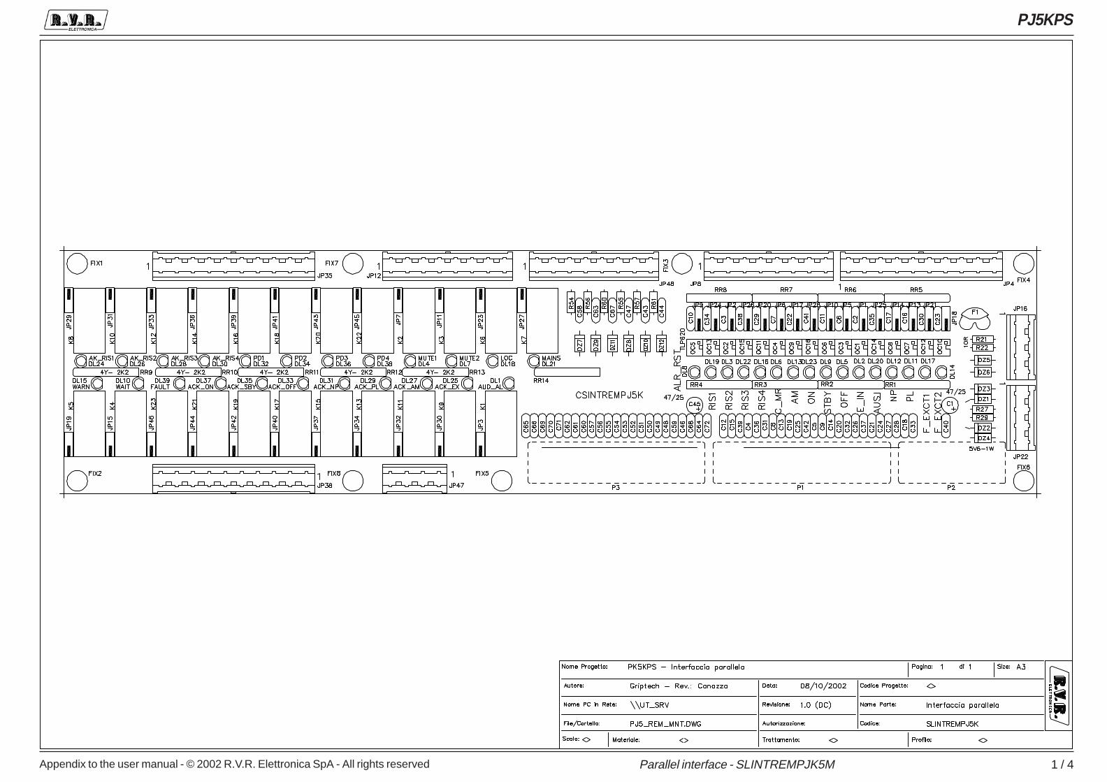
Appendix to the user manual - © 2002 R.V.R. Elettronica SpA - All rights reserved
PJ5KPS
1 / 4Parallel interface - SLINTREMPJK5M

Appendix to the user manual - © 2002 R.V.R. Elettronica SpA - All rights reserved
PJ5KPS
2 / 4Parallel interface - SLINTREMPJK5M
5
5
4
4
3
3
2
2
1
1
D D
C C
B B
A A
PJ5KMC
<>
2
CLAUDIO - Rev.: Canazza
INTERFACCIA REMOTA
<Code>
<Path PC>
CSINTREMPJ5KM
8/11/01
A31
1.0 (DC)
� � � � � � � � � � � � �
� � � � � � � � � � � � � � � � � � �
� � � � � � � � � � � �
� � � � � � � � � � � � �
� � � � �
� � � � � � � �
� � � � � �
� � � � � � � � � �
� � � � � � � � � � �
� � � � � � � � � ��
PJ5K_ELET2
PJ5K_ELET2
+ 1 2 V
C _ R L 3
W A I T
W A R N
D A C 1DAC2DAC3DAC4DAC5DAC6
W A R N _ O C
A M _REM
F_EXCT1_REM
R I S 4_ IN_REM
PL_REM
MUTE2_OC
RST_AL_REM
S T D B Y _ R E M
MAINS_BUS
A U D _ A L R M _ O C
W A I T _ O C
EXT_INT_REM
O F F _ R E M
AUS_INT_REMMUTE1_OC
R I S 1_ IN_REM
F_EXCT2_REM
R I S 3_ IN_REM
L O C _ SEL
N P _ R E M
O N _ R E M
C H G _ M R _ R EMR I S 2_ IN_REM
L O C _ SEL
W A R N _ O C
MUTE2_OC
MUTE1_OC
MAINS_BUS
W A I T _ O C
EXT_INT_REM
O F F _ R E M
RST_AL_REM
PL_REM
AM_REM
RIS4_ IN_REM
RIS1_ IN_REM
RIS3_ IN_REM
O N _ R EM
N P _ R EM
RIS2_ IN_REM
C H G _ M R _ R EM
F_EXCT1_REM
F_EXCT2_REM
AUS_INT_REM
STDBY_REM
EXT_INT
O F F
A L R _ R S T
PL
R I S 4
R I S 1
R I S 3
RIS2
C H G _ M R
S T D BY
N P
AM
MAINS_BUS
A U D _ A L R M _ OC
L O C _ SEL
O N
AM
O N
R I S 2
C H G _ M R
S T D BY
F_EXCT2
N PAU S_INT
F_EXCT1
R I S 3
R I S 1
EXT_INTO F F
R I S 4
A L R _ R S T
MUTE1C_MUTE2
MAINS
STR+STR-
STR+
STR-
C_RL3
A U D _ A L R M _ OC
MUTE1_OC
W A R N _ O C
C _ A U D _ A L A R MA U D _ A L R M
W A R N
W A I T
D A C1D A C2D A C3
D A C5D A C6
C_MUTE1
MUTE2
L O C
D A C2
D A C5D A C6
D A C4
D A C1
D A C3
D A C4
C_RL3
W A I T
A U D _ A L R M
W A R N
C_RL3
M U TE2
C_RL3
C _ A U D _ A L A R M
M U TE1
C_MUTE2
C_MUTE1
MAINS
W A I T _ O C
C _ L O C
C_MAINS
L O C
C_MAINS
C _ L O C
F_EXCT1
A U S_INT
F_EXCT2
PL
MUTE2_OC
+12V
+12V
+12V
+12V
+12V
+12V
+12V
+12V
+12V
+12V
+12V
+12V
+12V
+12V
+12V
+12V +12V
+12V
+12V
+12V
+12V
+12V
+12V
+12V
+12V
C264K7pF
12
C 2
4K7pF
12
R R 9 D2K2
78
C 6
4K7pF
12
O C 1 6
TLP620
1
2
4
3
R R 2 D
47R
78
FIX2
FIX35
1
O C 1 0
TLP620
1
2
4
3
C184K7pF
12
R R 1 3C2K2
56
FIX5
FIX35
1
DL17
D 3 -V
C394K7pF
12
C324K7pF
12
R R 4A
47R
12
C34
4K7pF
12
JP2
JUMPER3
13
2
K5
Z F H - 12V
1 311
9
46
81
16
R R 2A
47R
12
FIX1
FIX35
1
D Z 4
5V6-1W
C154K7pF
12
JP16
KB4
1234
C30
4K7pF
12
JP21
JUMPER3
13
2 R2910R
JP10
JUMPER3
13
2
JP7JUMPER3
13
2
D Z 35V6-1W
JP5
JUMPER3
13
2
K1
Z F H - 12V
1 311
9
46
81
16
JP18
JUMPER3
13
2
C244K7pF
12
DL10D3-V
O C 9
TLP620
1
2
4
3
C124K7pF
12
JP24
JUMPER3
13
2
C334K7pF
12
R R 6 D 1K5
78
R R 3 C
47R
56
C194K7pF
12
C 54K7pF
12
C10
4K7pF
12
JP27JUMPER3
13
2JP47
KB4
1234
R R 4B
47R
34
O C 1 4
TLP620
1
2
4
3
C424K7pF
12
R R 5A 1K5
12
R R 3B
47R
34
JP11JUMPER3
13
2
R R 1 D
47R
78
C38
4K7pF
12
R R 2B
47R
34
O C 8
TLP620
1
2
4
3
K6
Z F H - 12V
1 311
9
46
81
16
D Z 2
12V-1W
JP4
K B 10
12345678910
R R 1 4D2K2
78
JP9
JUMPER3
13
2
C144K7pF
12
F IX3
FIX35
1
DL15D3-V
R2210R
DL5
D 3 -V
DL3
D 3 -V
FIX6
FIX35
1
O C 1 1
TLP620
1
2
4
3
DL11
D 3 -V
R R 6 C 1K5
56
JP26
JUMPER3
13
2
C254K7pF
12
DL16
D 3 -V
C 94K7pF
12
C274K7pF
12
FIX8
FIX35
1
DL9
D 3 -VJP12
KB8
12345678
R R 8 A 1K5
12
C16
4K7pF
12
DL1D3-V
DL22
D 3 -V
O C 1
TLP620
1
2
4
3
JP8
KB8
12345678
JP15JUMPER3
13
2
JP22
KB4
1234
JP6
JUMPER3
13
2
JP48
KB8
12345678
R R 5 C 1K5
56
C41
4K7pF
12
DL14
D 3 -V
K2
Z F H - 12V
1 311
9
46
81
16
C17
4K7pF
12
R R 2 C
47R
56
C404K7pF
12
O C 1 2
TLP620
1
2
4
3
O C 3
TLP620
1
2
4
3
R R 3A
47R
12
JP13
JUMPER3
13
2
P2
D B 9 MASCHIO
594837261
R R 8 C 1K5
56
R R 7 D 1K5
78
DL20
D 3 -V
C204K7pF
12
O C 1 3
TLP620
1
2
4
3
DL18D3-V
R R 4 D
47R
78
D Z 112V-1W
JP28
JUMPER3
13
2
C314K7pF
12
K7
Z F H - 12V
1 311
9
46
81
16
JP3JUMPER3
13
2
R R 4 C
47R
56
R R 1B
47R
34
R2710R
C22
4K7pF
12
JP25
JUMPER3
13
2
K3
Z F H - 12V
1 311
9
46
81
16
RR14B2K2
34
R R 7 A 1K5
12
+C 147/25
JP19JUMPER3
13
2
FIX4
FIX35
1
C284K7pF
12
C 44K7pF
12
O C 6
TLP620
1
2
4
3
R R 8B 1K5
34
C 3
4K7pF
12
JP14
JUMPER3
13
2
R R 3 D
47R
78
C11
4K7pF
12
R R 7 C 1K5
56
R R 1A
47R
12
O C 5
TLP620
1
2
4
3
C374K7pF
12
F IX7
FIX35
1
JP17
JUMPER3
13
2
C 84K7pF
12
C35
4K7pF
12
DL4D3-V
R R 8 D 1K5
78
R R 5 D 1K5
78
R2110R
O C 1 5
TLP620
1
2
4
3
R R 1 4C
2K2
5 6
C364K7pF
12
R R 9B2K2
34
C214K7pF
12
DL2
D 3 -V
C29
4K7pF
12
O C 4
TLP620
1
2
4
3
K4
Z F H - 12V
1 311
9
46
81
16
P1
D B 25 FEMMINA
1 325122411231022
921
820
719
618
517
416
315
214
1
R R 7 B 1K5
34
R R 1 C
47R
56
RR13A2K2
12
R R 5B 1K5
34
DL8
D 3 -V
R R 6A 1K5
12
DL21D3-V
DL6
D 3 -V
DL13
D 3 -V
f
F 1DSS-308
1 3
2
JP1
JUMPER3
13
2
C 7
4K7pF
12
JP23JUMPER3
13
2
DL19
D 3 -V
DL7D3-V
O C 7
TLP620
1
2
4
3
JP20
JUMPER3
13
2
DL23
D 3 -V
DL12
D 3 -V
O C 2
TLP620
1
2
4
3
C134K7pF
12
RR14A2K2
12
R R 6 B 1K5
34
C23
4K7pF
12
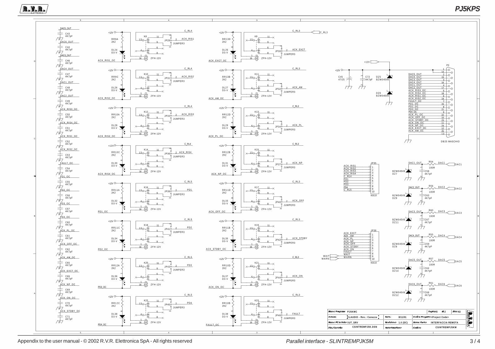
Appendix to the user manual - © 2002 R.V.R. Elettronica SpA - All rights reserved
PJ5KPS
3 / 4Parallel interface - SLINTREMPJK5M
5
5
4
4
3
3
2
2
1
1
D D
C C
B B
A A
PJ5KMC
<Project Code>
2
CLAUDIO - Rev.: Canazza
INTERFACCIA REMOTA
CSINTREMPJ5K.DSN
\\UT_SRV
CSINTREMPJ5KM
8/11/01
A32
1.0 (DC)
� � � � � � � � � � � � �
� � � � � � � � � � � � � � � � � � �
� � � � � � � � � � � �
� � � � � � � � � � � � �
� � � � �
� � � � � � � �
� � � � � �
� � � � � � � � � �
� � � � � � � � � � �
� � � � � � � � � ��
A C K_RIS1
A C K_STDBY_OC
F A ULT_OC
D A C3
C _ RL5
P D 1 _ O C
A C K _P L_OC
D A C4
A C K_RIS4_OC
A C K_RIS3_OC
W A R N
DAC5_OUT
A C K_RIS3
DAC1_OUT
P D 1 _ O C
A C K _ PL
P D 4
DAC4_OUT
A C K_RIS1
A C K _ A M_OC
F A ULT
D A C6
DAC6_OUT
DAC4_OUT
P D 3
DAC5_OUT
D A C1
C _ RL4A C K_RIS4_OC
A C K_RIS1_OC
P D 2 _ O C
A C K _EXCT
DAC3_OUT
DAC5_OUT
DAC3_OUT
FAULT_OC
A C K_RIS4_OC
A C K_RIS2_OC
A C K _ O F F _ O C
P D 2
P D 3 _ O C
A C K _ N P _ O C
DAC1_OUT
C_RL5
DAC3_OUT
A C K _ O F F _ O C
C_RL4
P D 3
A C K _ E X CT_OC
A C K_RIS3
P D 1
P D 4 _ O C
PD4_OC
A C K_STDBY
C_RL5
P D 2
PD4
P D 2 _ O C
C_RL5
A C K _ N P
A C K _ N P _ O C
DAC2_OUT
P D 3 _ O C
A C K_RIS4
C_RL5
A C K_RIS2_OC
DAC1_OUT
A C K _ O N _ O C
C_RL4
A C K_RIS3_OC
A C K _ O N
ACK _AM
DAC6_OUT
P D 1
A C K_OFF
A C K_RIS4
A C K _ E X CT_OC
A C K _ O N _ O C
A C K_RIS3_OC
DAC2_OUT
A C K _STDBY_OC
A C K _ O F F _ O C
A C K_RIS2
A C K _ E X CT_OC
W A I T
A C K_RIS1_OC
A C K _ A M _OC
DAC6_OUT
ACK_PL_OC
DAC4_OUT
DAC2_OUT
C_RL4
C_RL4
A C K_RIS2
A C K _ A M_OC
A C K _ N P _ O C
D A C2
A C K_RIS1_OC
A C K_RIS2_OC
P D 1 _ O C
PD3_OC A C K _ O N _ O C
P D 2 _ O C
PD4_OC
A C K _STDBY_OC
D A C5
A C K_STDBY
C_RL3
A C K _EXCT
C_RL3
C_RL3
C_RL3
A C K _ N P
A C K_AM
C_RL3
A C K _ O N
C_RL3
C_RL3
F A ULT_OC
A C K_OFF
FAULT
C_RL3
ACK_PL_OC
A C K _ PL
+12V
+12V
+12V
+12V
+12V
+12V
+12V
+12V
+12V
+12V
+12V
+12V
+12V
+12V
+12V
+12V
+12V
R R 1 3D2K2
78
R R 9 C2K2
56
K15
Z F H -12V
1 311
9
46
81
16
+C4547/25
R R 13B2K2
34
C714K7pF
12
DL24D 3 -V
DL38D 3 -V
C694K7pF
12
K22
Z F H -12V
1 311
9
46
81
16
C624K7pF
12
R R 1 2D2K2
78
JP39JUMPER3
13
2
DL26D 3 -V
K10
Z F H -12V
1 311
9
46
81
16
R R 12B2K2
34
C664K7pF
12
JP41JUMPER3
13
2
C644K7pF
12
JP33JUMPER3
13
2
DL31D 3 -V
C724K7pF
12
K23
Z F H -12V
1 311
9
46
81
16
JP36JUMPER3
13
2
JP29JUMPER3
13
2
C594K7pF
12
DL29D 3 -V
R R 1 1D2K2
78
C574K7pF
12
D Z 11B Z W 0 45V8
JP34JUMPER3
13
2
JP37JUMPER3
13
2
D Z 9B Z W 0 45V8
C434K7pF
12
DL27D 3 -V
R60
100R
R R 11B2K2
34
DL36D 3 -V
K20
Z F H -12V
1 311
9
46
81
16
K19
Z F H -12V
1 311
9
46
81
16
C514K7pF
12
R R 1 0D2K2
78
JP40JUMPER3
13
2
K12
Z F H -12V
1 311
9
46
81
16
C504K7pF
12
DL35D 3 -V
R57
100R
D Z 7B Z W 0 45V8
R54
100R
JP42JUMPER3
13
2
R55
100R
C484K7pF
12
C494K7pF
12
D Z 5B Z W 0 45V8
D Z 6B Z W 0 45V8
R R 10B2K2
34
K16
Z F H -12V
1 311
9
46
81
16
D Z 8B Z W 0 45V8
C584K7pF
12
JP45JUMPER3
13
2
DL34D 3 -V
K14
Z F H -12V
1 311
9
46
81
16
DL39D 3 -V
JP31JUMPER3
13
2
C614K7pF
12
C554K7pF
12
DL33D 3 -V
DL32D 3 -V
JP32JUMPER3
13
2
K13
Z F H -12V
1 311
9
46
81
16
DL25D 3 -V
C464K7pF
12
C544K7pF
12
C564K7pF
12
K8
Z F H -12V
1 311
9
46
81
16
C634K7pF
12
K18
Z F H -12V
1 311
9
46
81
16
C654K7pF
12
D Z 12B Z W 0 45V8 C68
4K7pF
12
DL30D 3 -V
JP35
K B 10
12345678910
JP43JUMPER3
13
2
C704K7pF
12
JP46JUMPER3
13
2
K9
Z F H -12V
1 311
9
46
81
16
C534K7pF
12
DL28D 3 -V
R56
100R
JP30JUMPER3
13
2C444K7pF
12
R61
100R
P3
D B 25 MASCHIO
1 325122411231022
921
820
719
618
517
416
315
214
1
C604K7pF
12
K21
Z F H -12V
1 311
9
46
81
16
K11
Z F H -12V
1 311
9
46
81
16
D Z 10B Z W 0 45V8
C524K7pF
12
C474K7pF
12
C674K7pF
12
JP38
K B 10
12345678910
DL37D 3 -V
R R 1 1 C2K2
56
R R 11A2K2
12
R R 12A2K2
12
R R 1 0 C2K2
56
JP44JUMPER3
13
2
R R 1 2 C2K2
56
R R 10A2K2
12
K17
Z F H -12V
1 311
9
46
81
16
R R 9A2K2
12
+12V
W A I TW A R N
D A C1
D A C2
D A C3
D A C4
D A C6
D A C5
C_RL3
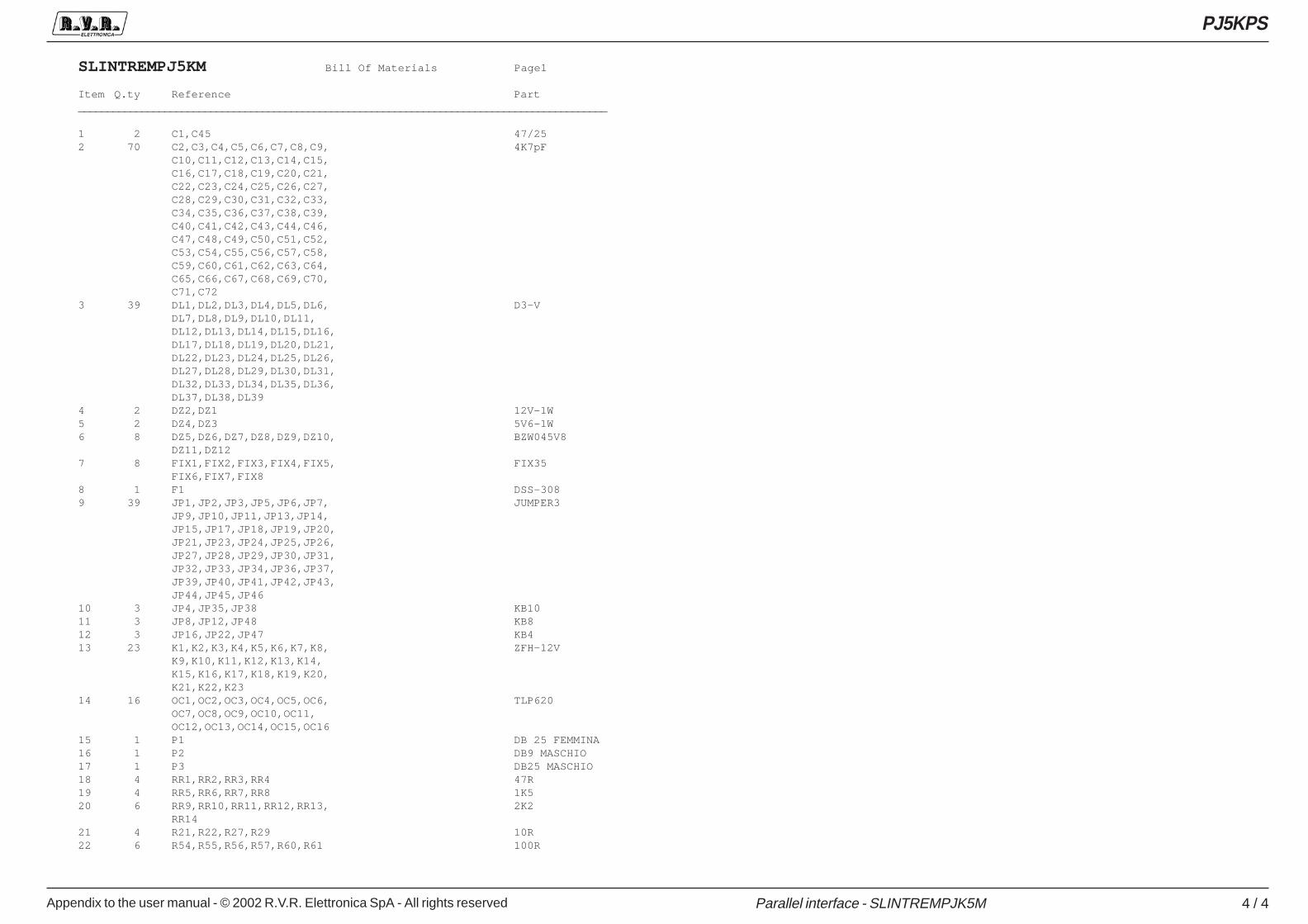
Appendix to the user manual - © 2002 R.V.R. Elettronica SpA - All rights reserved
PJ5KPS
4 / 4Parallel interface - SLINTREMPJK5M
SLINTREMPJ5KM Bill Of Materials Page1
Item Q.ty Reference Part____________________________________________________________________________________________
1 2 C1,C45 47/252 70 C2,C3,C4,C5,C6,C7,C8,C9, 4K7pF
C10,C11,C12,C13,C14,C15,C16,C17,C18,C19,C20,C21,C22,C23,C24,C25,C26,C27,C28,C29,C30,C31,C32,C33,C34,C35,C36,C37,C38,C39,C40,C41,C42,C43,C44,C46,C47,C48,C49,C50,C51,C52,C53,C54,C55,C56,C57,C58,C59,C60,C61,C62,C63,C64,C65,C66,C67,C68,C69,C70,C71,C72
3 39 DL1,DL2,DL3,DL4,DL5,DL6, D3-VDL7,DL8,DL9,DL10,DL11,DL12,DL13,DL14,DL15,DL16,DL17,DL18,DL19,DL20,DL21,DL22,DL23,DL24,DL25,DL26,DL27,DL28,DL29,DL30,DL31,DL32,DL33,DL34,DL35,DL36,DL37,DL38,DL39
4 2 DZ2,DZ1 12V-1W5 2 DZ4,DZ3 5V6-1W6 8 DZ5,DZ6,DZ7,DZ8,DZ9,DZ10, BZW045V8
DZ11,DZ127 8 FIX1,FIX2,FIX3,FIX4,FIX5, FIX35
FIX6,FIX7,FIX88 1 F1 DSS-3089 39 JP1,JP2,JP3,JP5,JP6,JP7, JUMPER3
JP9,JP10,JP11,JP13,JP14,JP15,JP17,JP18,JP19,JP20,JP21,JP23,JP24,JP25,JP26,JP27,JP28,JP29,JP30,JP31,JP32,JP33,JP34,JP36,JP37,JP39,JP40,JP41,JP42,JP43,JP44,JP45,JP46
10 3 JP4,JP35,JP38 KB1011 3 JP8,JP12,JP48 KB812 3 JP16,JP22,JP47 KB413 23 K1,K2,K3,K4,K5,K6,K7,K8, ZFH-12V
K9,K10,K11,K12,K13,K14,K15,K16,K17,K18,K19,K20,K21,K22,K23
14 16 OC1,OC2,OC3,OC4,OC5,OC6, TLP620OC7,OC8,OC9,OC10,OC11,OC12,OC13,OC14,OC15,OC16
15 1 P1 DB 25 FEMMINA16 1 P2 DB9 MASCHIO17 1 P3 DB25 MASCHIO18 4 RR1,RR2,RR3,RR4 47R19 4 RR5,RR6,RR7,RR8 1K520 6 RR9,RR10,RR11,RR12,RR13, 2K2
RR1421 4 R21,R22,R27,R29 10R22 6 R54,R55,R56,R57,R60,R61 100R
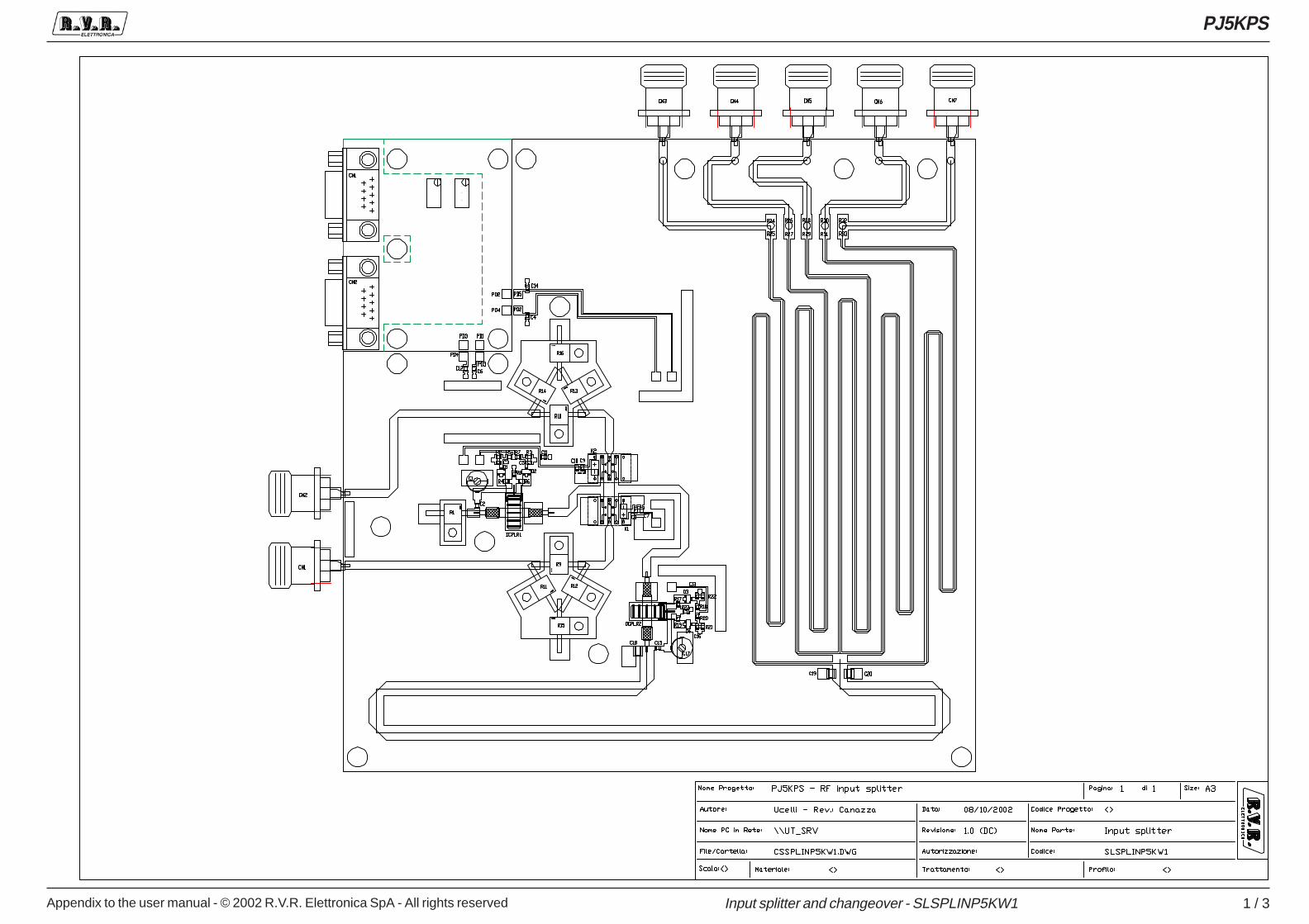
Appendix to the user manual - © 2002 R.V.R. Elettronica SpA - All rights reserved
PJ5KPS
1 / 3Input splitter and changeover - SLSPLINP5KW1
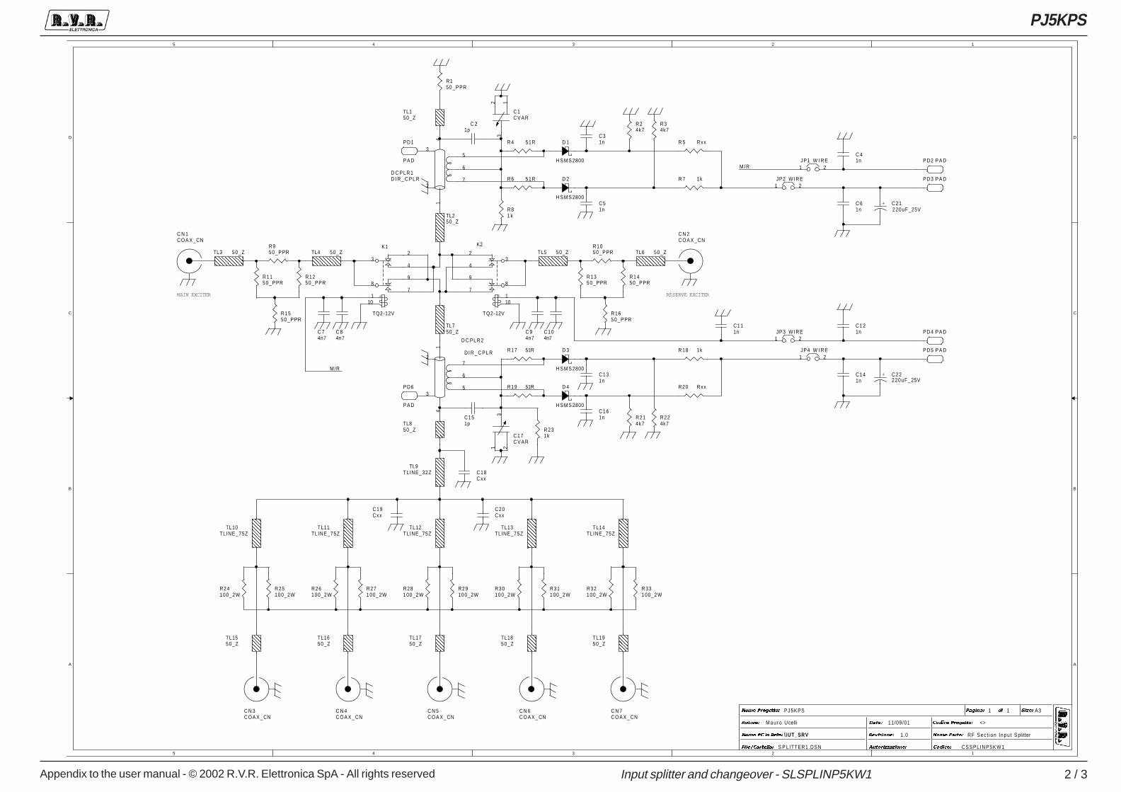
Appendix to the user manual - © 2002 R.V.R. Elettronica SpA - All rights reserved
PJ5KPS
2 / 3Input splitter and changeover - SLSPLINP5KW1
5
5
4
4
3
3
2
2
1
1
D D
C C
B B
A A
MAIN EXCITER RESERVE EXCITER
\ \UT_SRV RF Sec t i on Inpu t Splitter
CSSPLINP5K W 1
1.0
PJ5KPS
<>
S P LITTER1.DSN
M a u r o U celli 11/09/01
11 A3
� � � � � � � � � � � � �
� � � � � � � � � � � � � � � � � � �
� � � � � � � � � � � �
� � � � � � � � � � � � �
� � � � �
� � � � � � � �
� � � � � �
� � � � � � � � � �
� � � � � � � � � � �
� � � � � � � � � ��
M/R
M / R
TL750_Z
R1650_PPR
D 3
H S M S 2800
TL1650_Z
C31n
R1050_PPR
R81 k
TL1750_Z
C51n
D C PLR1D I R _ C P L R
1
2
3
4
7
6
5
TL1850_Z
R34k7
C104n7
C18Cxx
C 21p
TL1950_Z
TL850_Z
R26100_2W
D 4
H S M S 2800
C131n
R 7 1k
R27100_2W
R25100_2W
R28100_2W
C121n
TL5 50_Z
R29100_2W
R30100_2W
C20Cxx
+
K1
TQ2-12V
32
4
89
71
10
R31100_2W
C19Cxx
C 94n7
R32100_2W
C 61n
JP3 W I R E1 2
R1150_PPR
R33100_2W
JP4 W I R E1 2
TL250_Z
TL6 50_Z
R1250_PPR
JP2 W I R E1 2
R1550_PPR
P D 2 P A DJP1 W I R E1 2
D 1
H S M S 2800
TL3 50_Z
D 2
H S M S 2800
R19 51R
R950_PPR
TL150_Z
R17 51R
C 84n7
+ C21220uF_25V
+ C22220uF_25V
C161n R22
4k7
TL4 50_Z
C N 3C O A X _ CN
P D 4 P A D
C141n
D C PLR2
D I R _ C P L R
1
2
3
4
7
6
5
R214k7
C N 4C O A X _ CN
C N 5C O A X _ CN
TL9TLINE_32Z
C N 6C O A X _ CN
P D 3 P A D
P D 1
P A D
C N 7C O A X _ CN
R18 1k
P D 6
P A D
R 5 Rxx
P D 5 P A D
C1C V A R
312
C111n
TL10TLINE_75Z
R4 51R
C17C V A R
31 2
+
K2
TQ2-12V
32
4
89
7110
R20 Rxx
R6 51R
TL11TLINE_75Z
C 41n
TL12TLINE_75Z
R150_PPR
TL13TLINE_75Z
R1350_PPR
C151p
TL14TLINE_75Z
R24100_2W
R1450_PPR
C N 1C O A X _CN
R231k
R24k7
C 74n7
TL1550_Z
C N 2C O A X _ CN
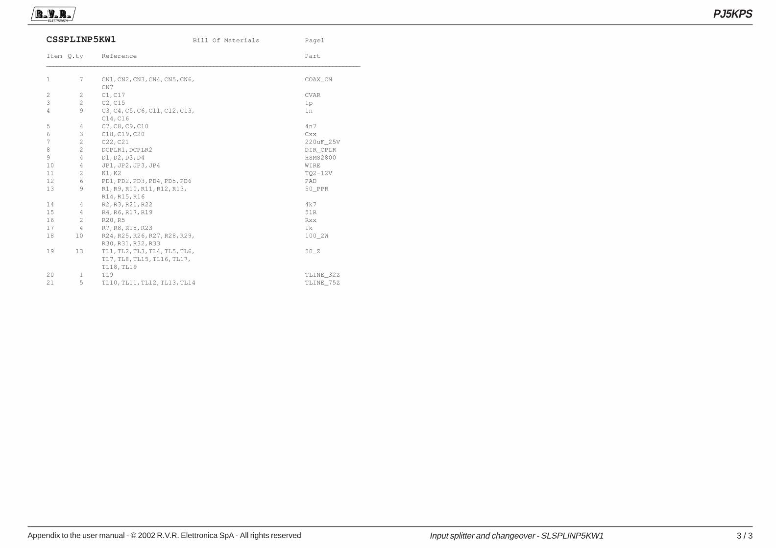
Appendix to the user manual - © 2002 R.V.R. Elettronica SpA - All rights reserved
PJ5KPS
3 / 3Input splitter and changeover - SLSPLINP5KW1
CSSPLINP5KW1 Bill Of Materials Page1
Item Q.ty Reference Part____________________________________________________________________________________________
1 7 CN1,CN2,CN3,CN4,CN5,CN6, COAX_CNCN7
2 2 C1,C17 CVAR3 2 C2,C15 1p4 9 C3,C4,C5,C6,C11,C12,C13, 1n
C14,C165 4 C7,C8,C9,C10 4n76 3 C18,C19,C20 Cxx7 2 C22,C21 220uF_25V8 2 DCPLR1,DCPLR2 DIR_CPLR9 4 D1,D2,D3,D4 HSMS280010 4 JP1,JP2,JP3,JP4 WIRE11 2 K1,K2 TQ2-12V12 6 PD1,PD2,PD3,PD4,PD5,PD6 PAD13 9 R1,R9,R10,R11,R12,R13, 50_PPR
R14,R15,R1614 4 R2,R3,R21,R22 4k715 4 R4,R6,R17,R19 51R16 2 R20,R5 Rxx17 4 R7,R8,R18,R23 1k18 10 R24,R25,R26,R27,R28,R29, 100_2W
R30,R31,R32,R3319 13 TL1,TL2,TL3,TL4,TL5,TL6, 50_Z
TL7,TL8,TL15,TL16,TL17,TL18,TL19
20 1 TL9 TLINE_32Z21 5 TL10,TL11,TL12,TL13,TL14 TLINE_75Z
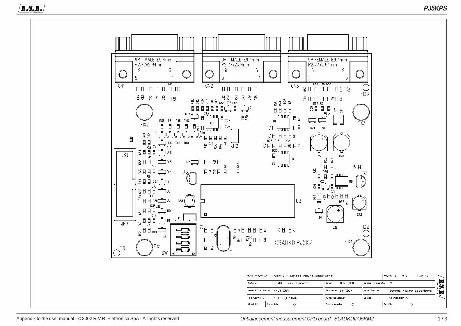
Appendix to the user manual - © 2002 R.V.R. Elettronica SpA - All rights reserved
PJ5KPS
1 / 3Unbalancement measurement CPU board - SLADKDIPJ5KM2
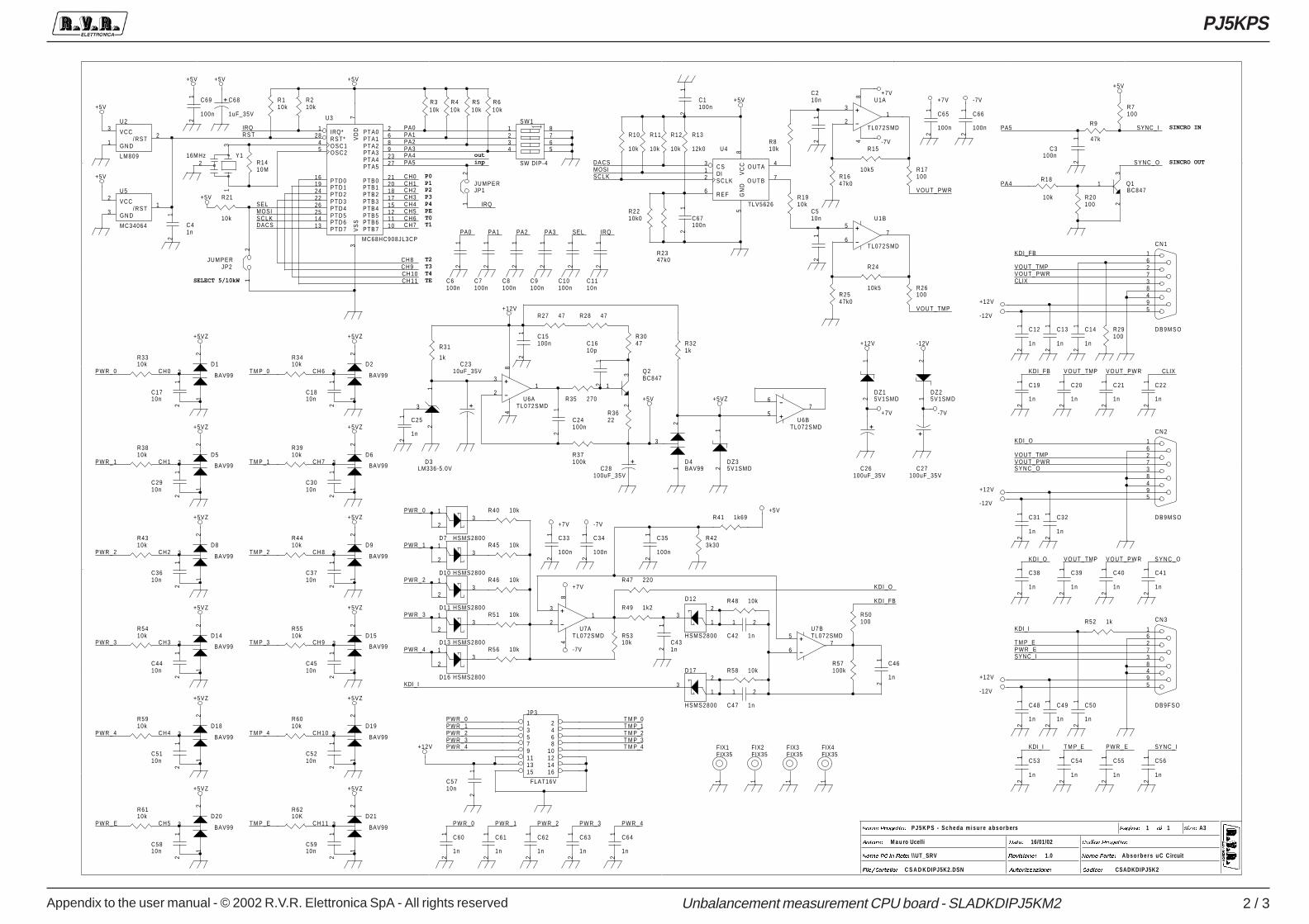
Appendix to the user manual - © 2002 R.V.R. Elettronica SpA - All rights reserved
PJ5KPS
2 / 3Unbalancement measurement CPU board - SLADKDIPJ5KM2
5
5
4
4
3
3
2
2
D D
C C
B B
A A
SINCRO IN
SINCRO OUT
P3
inp
T2
P4
SELECT 5/10kW
out
T3
PE
P1
T4
T1
P2
TE
P0
T0
\ \UT_SRV A b s o r b e r s u C C ircuit
CSADKDIPJ5K2
1.0
P J 5 K P S - S c h e d a m i s u r e a b s o r b ers
C S A D K DI PJ5K2.DSN
M a u ro Ucelli 16/01/02
11 A31RPH 3URJHWWR�
$XWRUH� &RGLFH 3URJHWWR�
1RPH 3& LQ 5HWH�
)LOH�&DUWHOOD�
'DWD�
5HYLVLRQH�
&RGLFH�
1RPH 3DUWH�
$XWRUL]]D]LRQH�
3DJLQD� 6L]H�GL
PWR_4
P W R _ E
T M P _0
T M P _1
PWR_3
PWR_2
PWR_0
PWR_1
T M P _E
T M P _4
T M P _2
T M P _3
V O U T _ P W R
VOUT_TMP
SYNC_I
SYNC_O
PA4
CH4 IRQ
CH1
CH2
DACS
SEL
CH7CH6
IRQ
CH6
CH4
CH5
PA3
CH0
MOSI
CH2
CH10
PA1
PA5
CH9
DACS
PA0
CH11
PA5
CH0
PA2
CH8
PA2
SCLK
PA0
CH5
PA4
CH7
PA1
CH1
SEL
CH3
CH8CH9
SCLK
MOSI
CH3
IRQ
CH11CH10
R S T
PA3
PWR_0
PWR_1
PWR_2
PWR_3
PWR_4
KDI_I
KDI_O
KDI_FB
KDI_FB
VOUT_TMPV O U T _ P W RCLIX
KDI_FB V O U T _ P W R CLIX
KDI_O
V O U T _ P W RSYNC_O
KDI_O V O U T _ P W R S Y N C _ O
KDI_I
P W R _ EKDI_I
P W R _ ET M P _E
SYNC_I
SYNC_I
VOUT_TMP
VOUT_TMP
T M P_E
VOUT_TMP
PWR_0PWR_1PWR_2PWR_3PWR_4
T M P_0T M P_1T M P_2T M P_3T M P_4
PWR_0 PWR_1 PWR_2 PWR_3 PWR_4
+5V
+5VZ
+5VZ
+5VZ
+5VZ
+5VZ
+5VZ
+5VZ
+5VZ
+5VZ
+5VZ
+5VZ
+5VZ
+7V
-7V
+12V
+5V +5VZ
+5V+5V
+5V
+5V
+5V
-7V
+5V
-7V
+7V
+7V
+12V
-12V
+12V
-12V
+12V -12V
+7V -7V
+12V
-12V
+12V
+7V -7V
+5V+5V
C39
1n
12
D9
BAV99
12
3
+
C27100uF_35V
R423k30
R6210K
R4310k
JP2JUMPER
12
JP1JUMPER
12
C40
1n
12
C60
1n
12
R13
12k0
C10100n
12
R41 1k69
C48
1n
12
C69
100n
12
R46 10kC41
1n
12
U3
MC68HC908JL3CP
1
3
45
7
101112
1314
1517182021
2224
2526
2826892327
1619
IRQ*
VS
S
OSC1OSC2
VD
D
P T B 7P T B 6P T B 5
P T D 7P T D 6
P T B 4P T B 3P T B 2P T B 1P T B 0
P T D 3P T D 2
P T D 5P T D 4
RST*PTA0PTA1PTA2PTA3PTA4PTA5
P T D 0P T D 1
R2210k0
D21
BAV99
12
3
D17
HSMS2800
1
23
C53
1n
12
R11
10k
+
-
U1B
TL072SMD
5
67
CN2
D B 9 M S O
594837261
C64
1n
12
C4510n
12
R7100
C54
1n
12
C22
1n
12
D1
BAV99
12
3
D20
BAV99
12
3
DZ15V1SMD2
1
R51 10k
C49
1n
12
R3910k
C42 1n
1 2
R9
47k
R5410k
DZ25V1SMD
21
C5810n
12
C65
100n
12
R2347k0
D10 HSMS2800
1
23
+
-U6A
TL072SMD
3
21
48
C55
1n
12
C47 1n
1 2
+
-
U6BTL072SMD
5
67
R50100
R31
1k
C8100n
12
+
-
U1A
TL072SMD
3
21
84
D4BAV991
2
3
C5210n
12
C56
1n
12
C13
1n
12
R56 10k
Y116MHz
13
2
DZ35V1SMD2
1
C2910n
12
R48 10k
C14
1n
12
D15
BAV99
12
3
C34
100n
12
C50
1n
12
C12
1n
12
R58 10k
R52 1k
C24100n
12
C9100n
12
C1110n
12
C431n
12
C210n
12
CN3
DB9FSO
594837261
R28 47
R210k
R3410k
R2547k0
D12
HSMS2800
1
23
C3610n
12
D11 HSMS2800
1
23
R27 47
R17100
R49 1k2
C61
1n
12
D8
BAV99
12
3
D13 HSMS2800
1
23
R26100
U2
LM809
3
12VCC
G N D/RST R8
10k
R410k
C5910n
12
C19
1n
12+
C2310uF_35V
D3LM336-5.0V
2
3
1
C41n
12
Q1BC847
1
23
R20100
C33
100n1
2
Q2BC847
3
1
2
U4
TLV5626
312
6
4
7
85
CSDISCLK
REF
OUTA
O U T B
VC
CG
ND
R35 270
D2
BAV99
12
3
R12
10k
+ C68
1uF_35V
R3622
C20
1n
12
R37100k
+
-U7A
TL072SMD
3
21
48
C15100n
12
C3710n
12
+
-
U7BTL072SMD5
67
R1910k
C4410n
12
R57100k
C62
1n
12
R6110k
CN1
D B 9 M S O
594837261
R24
10k5
R5510k
D19
BAV99
12
3
C3010n
12
R10
10k
R510k
R4410k
U5
MC34064
2
31VCC
G N D/RST
C5110n
12
C66
100n
12
R5310k
D5
BAV99
12
3
C6100n
12
C1710n
12
R40 10k
R15
10k5
C1610p
12
R3047
D16 HSMS2800
1
23
C7100n
12
C46
1n
12
R310k
C25
1n
12
C67100n
12
R321k
R1410M
R3810k
R21
10k
+C28
100uF_35V
D14
BAV99
12
3
C1100n
12
C21
1n
12
C5710n
12
JP3
FLAT16V
1 23 45 67 89 1011 1213 1415 16
R3310k
D18
BAV99
12
3
C35
100n
12
C32
1n
12
+
C26100uF_35V
C63
1n
12
R6010k
C3100n
12
FIX1FIX35
1
C1810n
12
R110k
C31
1n
12
FIX2FIX35
1
D7 HSMS2800
1
23
R5910k
FIX3FIX35
1
R18
10k
C510n
12
R610k
D6
BAV99
12
3
C38
1n
12
R29100
FIX4FIX35
1
S W 1
SW DIP-4
1234
8765
R1647k0
R45 10k
R47 220

Appendix to the user manual - © 2002 R.V.R. Elettronica SpA - All rights reserved
PJ5KPS
3 / 3Unbalancement measurement CPU board - SLADKDIPJ5KM2
CSADKDIPJ5K2 Bill Of Materials Page1
Item Q.ty Reference Part____________________________________________________________________________________________
1 2 CN1,CN2 DB9MSO2 1 CN3 DB9FSO3 16 C1,C3,C6,C7,C8,C9,C10, 100n
C15,C24,C33,C34,C35,C65,C66,C67,C69
4 16 C2,C5,C11,C17,C18,C29, 10nC30,C36,C37,C44,C45,C51,C52,C57,C58,C59
5 31 C4,C12,C13,C14,C19,C20, 1nC21,C22,C25,C31,C32,C38,C39,C40,C41,C42,C43,C46,C47,C48,C49,C50,C53,C54,C55,C56,C60,C61,C62,C63,C64
6 1 C16 10p7 1 C23 10uF_35V8 3 C26,C27,C28 100uF_35V9 1 C68 1uF_35V10 3 DZ1,DZ2,DZ3 5V1SMD11 13 D1,D2,D4,D5,D6,D8,D9,D14, BAV99
D15,D18,D19,D20,D2112 1 D3 LM336-5.0V
13 7 D7,D10,D11,D12,D13,D16, HSMS2800D17
14 4 FIX1,FIX2,FIX3,FIX4 FIX3515 2 JP2,JP1 JUMPER16 1 JP3 FLAT16V17 2 Q2,Q1 BC84718 33 R1,R2,R3,R4,R5,R6,R8,R10, 10k
R11,R12,R18,R19,R21,R33,R34,R38,R39,R40,R43,R44,R45,R46,R48,R51,R53,R54,R55,R56,R58,R59,R60,R61,R62
19 6 R7,R17,R20,R26,R29,R50 10020 1 R9 47k21 1 R13 12k022 1 R14 10M23 2 R15,R24 10k524 3 R16,R23,R25 47k025 1 R22 10k026 3 R27,R28,R30 4727 3 R31,R32,R52 1k28 1 R35 27029 1 R36 2230 2 R57,R37 100k31 1 R41 1k6932 1 R42 3k3033 1 R47 22034 1 R49 1k235 1 SW1 SW DIP-436 3 U1,U6,U7 TL072SMD
37 1 U2 LM80938 1 U3 MC68HC908JL3CP39 1 U4 TLV562640 1 U5 MC3406441 1 Y1 16MHz

Appendix to the user manual - © 2003 R.V.R. Elettronica SpA - All rights reserved
PJ5KPS
1 / 5RF module CPU adapter/bias - SLADBSPJ5KPS2
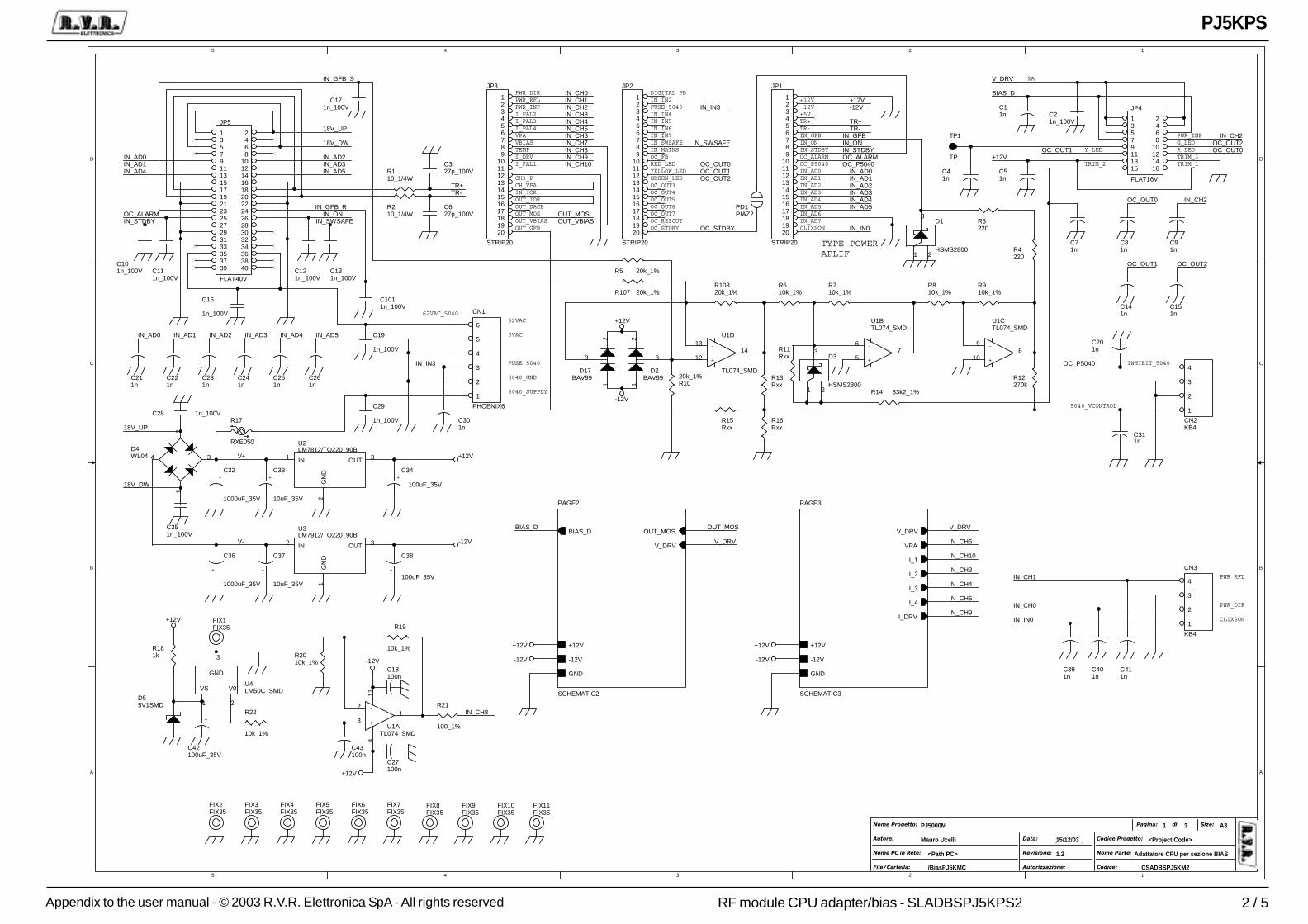
Appendix to the user manual - © 2003 R.V.R. Elettronica SpA - All rights reserved
PJ5KPS
2 / 5RF module CPU adapter/bias - SLADBSPJ5KPS2
5
5
4
4
3
3
2
2
1
1
D D
C C
B B
A A
OC_P5040
TYPE POWERAPLIF
IN_AD7IN_AD6
CLIXSON
IN_STDBY
FUSE 5040
CLIXSON
62VAC
0VAC
62VAC_5040
INHIBIT_5040
G_LEDY_LED R_LED
PWR_INP
TEMP
I_PAL1
I_PAL4
PWR_INP
CH_VPA
OUT_DACB
I_PAL3I_PAL2
VPAVBIAS
CH3_P
OC_STDBY
PWR_RFL
I_DRVIN_MAINS
OUT_GFB
OC_OUT4
OC_OUT6
OC_OUT3
OUT_VBIAS
GREEN_LED
OC_FB
DIGITAL FB
YELLOW_LED
IN_IOR
FUSE_5040
RED_LED
OC_OUT5
PWR_DIR
OUT_IOR
OC_OUT7
PWR_RFL
PWR_DIR
5040_SUPPLY
OC_RESOUT
IN IN2
IN IN4IN IN5IN IN6IN IN7IN SWSAFE
OUT MOS
+5V
+12V-12V
TR+TR-IN_GFBIN_ON
OC_ALARM
IN_AD0IN_AD1IN_AD2IN_AD3IN_AD4IN_AD5
TRIM_1TRIM_2TRIM_3
5040_VCONTROL
2A
5040_GND
PJ5000M
<Project Code>
3
Mauro Ucelli
Adattatore CPU per sezione BIAS
CSADBSPJ5KM2
<Path PC>
/BiasPJ5KMC
15/12/03
A31
1.2
�����������
����� ������������
������ �������
����� ������
���
���������
�����
���������
�������������
������ ������
PAGE2
SCHEMATIC2
OUT_MOSBIAS_D
+12V
GND
-12V
V_DRV
PAGE3
SCHEMATIC3
V_DRV
I_1
I_2
I_4
I_3
I_DRV
+12V
GND
-12V
VPA
IN_IN0
IN_AD0
+12V
IN_AD4
TR+
OC_ALARMOC_P5040
IN_AD5
IN_ON
OC_P5040
18V_DW
18V_UP
TR-
V_DRV
IN_CH2OC_OUT2OC_OUT0OC_OUT1
BIAS_DIN_CH0
IN_CH3
TR-IN_CH4
IN_CH10
IN_CH5
IN_CH2
IN_CH9
IN_CH1
IN_CH8
IN_CH6
OUT_MOSOUT_VBIAS
IN_CH7
OC_OUT0
IN_IN3
IN_IN3
IN_SWSAFE
OC_OUT1OC_OUT2
-12V
IN_AD1IN_AD2IN_AD3
IN_STDBY
OC_STDBY
IN_GFB
BIAS_D OUT_MOS V_DRV
IN_CH10
IN_CH3
IN_CH4
IN_CH5
IN_CH9
IN_CH6
18V_UP
TR+
18V_DW
IN_AD2IN_AD3IN_AD5
IN_ONIN_SWSAFE
IN_AD0IN_AD1IN_AD4
OC_ALARMIN_STDBY
IN_CH8
IN_GFB_R
IN_AD0 IN_AD1 IN_AD3 IN_AD4 IN_AD5IN_AD2
IN_IN0
IN_CH2OC_OUT0
OC_OUT1 OC_OUT2
V+
V-
IN_CH1
IN_CH0
V_DRV
+12V
IN_GFB_S
+12V
+12V
+12V
-12V
+12V
-12V
+12V
-12V
+12V
-12V
-12V
R1020k_1%
D2BAV99
12
3
FIX2FIX35
C91n
C111n_100V
R16Rxx
JP3
STRIP20
123456789
1011121314151617181920
R181k
FIX3FIX35
U3LM7912/TO220_90B
2 3
1
IN OUT
GN
D
C221n
JP5
FLAT40V
1 23 45 67 89 1011 1213 1415 1617 1819 2021 2223 2425 2627 2829 3031 3233 3435 3637 3839 40
U2LM7812/TO220_90B
1 3
2
IN OUT
GN
D
C101n_100V
D4WL04
1
3
2
4
FIX4FIX35
JP4
FLAT16V
1 23 45 67 89 1011 1213 1415 16
C16
1n_100V
C11n
R4220
FIX5FIX35
R3220
+C32
1000uF_35V
R5 20k_1%
U4LM50C_SMD
1
3
2
VS
GND
V0
C21n_100V
C211n
+
C36
1000uF_35V
+C33
10uF_35V
FIX6FIX35
FIX7FIX35
+
-
U1D
TL074_SMD
12
1314
+
-
U1ATL074_SMD
3
21
114
CN2KB4
1
2
3
4
C131n_100V
C351n_100V
JP2
STRIP20
123456789
1011121314151617181920
R13Rxx
R610k_1%
+
C37
10uF_35V
C28 1n_100V
R710k_1%
FIX1FIX35
R22
10k_1%
CN1
PHOENIX6
1
2
3
4
5
6
C171n_100V
C18100n
C311n
C121n_100V
D17BAV99
12
3
R107 20k_1%
R110_1/4W
C1011n_100V
R11Rxx
C29
1n_100V
R10820k_1%
C201n
R810k_1%
R15Rxx
+
C42100uF_35V
R21
100_1%
C19
1n_100V
C261n
FIX8FIX35
C411n
C71n
FIX9FIX35
R12270k
FIX10FIX35
CN3
KB4
1
2
3
4
FIX11FIX35
+
C38
100uF_35V
+
-
U1CTL074_SMD
10
98
C151n
C251n
C627p_100V
C43100n
R17
RXE050
+C34
100uF_35V
C27100n
R910k_1%
D1
HSMS28001 2
3
JP1
STRIP20
123456789
1011121314151617181920
+
-
U1BTL074_SMD
5
67
R19
10k_1%
D3
HSMS28001 2
3
C141n
PD1PIAZ2
C401n
C241n
R2010k_1%
R210_1/4W
C391n
C51n
C41n
TP1
TP
D55V1SMD
C81n
C301n
R14 33k2_1%
C231n
C327p_100V
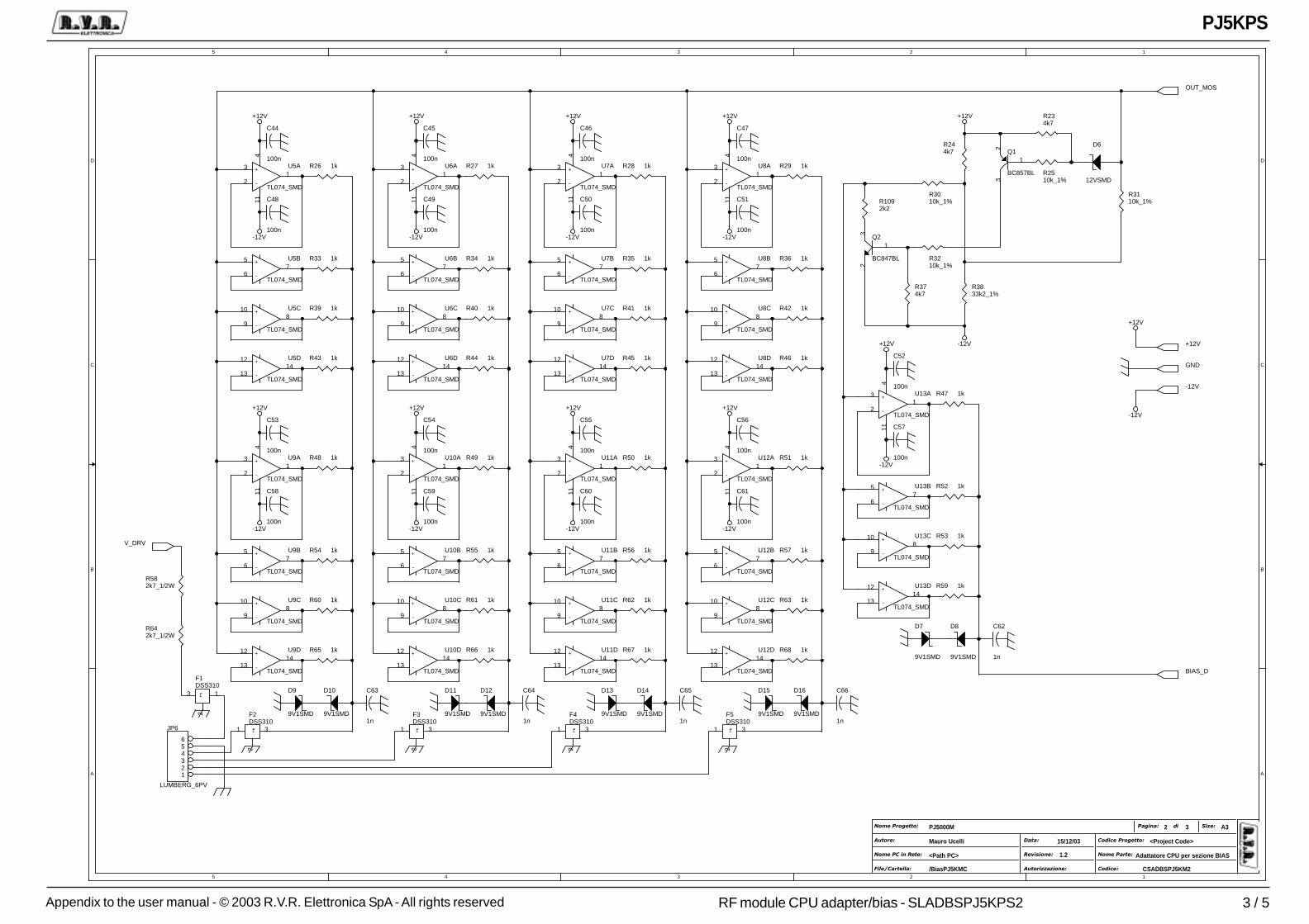
Appendix to the user manual - © 2003 R.V.R. Elettronica SpA - All rights reserved
PJ5KPS
3 / 5RF module CPU adapter/bias - SLADBSPJ5KPS2
5
5
4
4
3
3
2
2
1
1
D D
C C
B B
A A
PJ5000M
<Project Code>
3
Mauro Ucelli
Adattatore CPU per sezione BIAS
CSADBSPJ5KM2
<Path PC>
/BiasPJ5KMC
15/12/03
A32
1.2
�����������
����� ������������
������ �������
����� ������
���
���������
�����
���������
�������������
������ ������
-12V
+12V
-12V
+12V
-12V
-12V
+12V
+12V
-12V
-12V
+12V
+12V
-12V
-12V
+12V
+12V
-12V
+12V
-12V
+12V
+12V
-12V
R68 1k
D12
9V1SMD
C57
100n
+
-
U11D
TL074_SMD
12
1314
R27 1k+
-
U5A
TL074_SMD
3
21
114
R2510k_1%
+
-
U12B
TL074_SMD
5
67
D11
9V1SMD
R56 1k
R59 1k
+
-
U5B
TL074_SMD
5
67
R34 1k
+
-
U5C
TL074_SMD
10
98
R50 1k
+
-
U13D
TL074_SMD
12
1314
+
-
U5D
TL074_SMD
12
1314
R40 1k
C44
100n
D6
12VSMD
+
-
U11A
TL074_SMD
3
21
114
R53 1k
C48
100n
R44 1k
R3110k_1%
R62 1k
R47 1k
C54
100n
R244k7
C52
100n
R67 1k
R1092k2
C59
100n
+
-
U11B
TL074_SMD
5
67
+
-
U13B
TL074_SMD
5
67
+
-
U10C
TL074_SMD
10
98
R52 1k
+
-
U8A
TL074_SMD
3
21
114
+
-
U10D
TL074_SMD
12
1314
+
-
U13A
TL074_SMD
3
21
114
+
-
U8B
TL074_SMD
5
67
R55 1k
R234k7
+
-
U13C
TL074_SMD
10
98
+
-
U8C
TL074_SMD
10
98
R49 1k
R3010k_1%
JP6
LUMBERG_6PV
123456
+
-
U8D
TL074_SMD
12
1314
+
-
U10A
TL074_SMD
3
21
114
C47
100n
R61 1k
D14
9V1SMD
+
-
U9A
TL074_SMD
3
21
114
R3833k2_1%
C51
100n
R66 1k
+
-
U7A
TL074_SMD
3
21
114
D13
9V1SMD
+
-
U9B
TL074_SMD
5
67
R29 1k
+
-
U10B
TL074_SMD
5
67
R374k7
+
-
U7B
TL074_SMD
5
67
+
-
U9C
TL074_SMD
10
98
R36 1k
+
-
U7C
TL074_SMD
10
98
+
-
U9D
TL074_SMD
12
1314
f
F5DSS310
1 32
R42 1k
+
-
U7D
TL074_SMD
12
1314
C62
1n
f
F4DSS310
1 3
2
C53
100n
f
F3DSS310
1 3
2
R46 1k
C46
100nR26 1k
f
F2DSS310
1 3
2
C58
100n
R33 1k
R582k7_1/2W
C56
100n
C50
100n
R39 1k
R642k7_1/2W
R48 1k
R43 1k
C61
100n
R28 1k
D7
9V1SMD
R54 1k
C63
1n
+
-
U12C
TL074_SMD
10
98
R35 1k
D8
9V1SMD
+
-
U6A
TL074_SMD
3
21
114
R60 1k
C64
1n
Q2
BC847BL
3
1
2
R3210k_1%
+
-
U12D
TL074_SMD
12
1314
R41 1k
Q1
BC857BL
3
1
2
+
-
U6B
TL074_SMD
5
67
R65 1k
C65
1n
R57 1k
R45 1k
+
-
U6C
TL074_SMD
10
98
C66
1n
R51 1k
C55
100n
+
-
U6D
TL074_SMD
12
1314
D10
9V1SMD
+
-
U12A
TL074_SMD
3
21
114
D16
9V1SMD
C60
100n
C45
100n
D9
9V1SMD
R63 1k
D15
9V1SMD
+
-
U11C
TL074_SMD
10
98
f
F1DSS310
13
2C49
100n
OUT_MOS
BIAS_D
+12V
GND
-12V
V_DRV

Appendix to the user manual - © 2003 R.V.R. Elettronica SpA - All rights reserved
PJ5KPS
4 / 5RF module CPU adapter/bias - SLADBSPJ5KPS2
5
5
4
4
3
3
2
2
1
1
D D
C C
B B
A A
40A
10A
10A
10A
10A
2A
10A
10A
10A
10A
PJ5000M
<Project Code>
3
Mauro Ucelli
Adattatore CPU per sezione BIAS
CSADBSPJ5KM2
<Path PC>
/BiasPJ5KMC
15/12/03
A33
1.2
�����������
����� ������������
������ �������
����� ������
���
���������
�����
���������
�������������
������ ������
I3-
I4-
ID+
I2+
I3+
I4-
I3-
ID-
I4+
I1+
ID-
I2-
I2-
I1+
I2+
I3+
I4+
ID+
I1-
I1-
+12V
-12V
+12V
-12V
+12V +12V
+12V
-12V
-12V
-12V
+12V +12V
-12V
-12V
+12V
-12V
-12V
+12V
-12V
+12V
+12V
-12V
R90 100_1%
R102 10k_1%
PD5
PAD10A
R95 100k
R105 100k
TR150k_T4S
13
2
R9427k4_1/4W
R73 10k_1%
TR550k_T4S
13
2
R971k
R69 51_1%
C95
100n
C921n
R100 51_1%
R70 10k_1%
C701n_100V
C67
100n
U17INA146
2
3
4 1 8
6
57
C78
100n
R96 100k
R104
100_1%
C884n7_100V
C100
100n
C721n
C81680pHQ
C731n_100V
R86 51_1%
R76 100_1%
U18INA146
2
3
4 1 8
6
57
C83680pHQ
SH1 SHUNT2.5
R10610_1%
C89680pHQ
SH2 SHUNT2.5
R89 10k_1%
C751n
C764n7_100V
C96
100n
SH3 SHUNT2.5
R9910_1%
SH4 SHUNT2.5
PD2
PAD10A
C85
100n
CN4
KRA4
1
2
3
4
C871n_100V
R103 100_1%
TR450k_T4S
13
2
U14INA146
2
3
4 1 8
6
57
R101 10k_1%
R91 100_1%C911n
FS1
F2A_C
R93
100_1%
C691n_100V
R87 10k_1%
U15INA146
2
3
4 1 8
6
57
C931n
C804n7_100V
TR250k_T4S
13
2
U16INA146
2
3
4 1 8
6
57
R8210_1%
R74 10k_1%
TR350k_T4S
13
2
R71 51_1%
R80 100k
R88 10k_1%
PD3
PAD10A
C77680pHQ
C971n_100V
R72 10k_1%
R84 51_1%
C981n
C68
100n
R85 10k_1%
C79
100n
C861n_100V
R78
100_1%
C84
100n
TP2TP
C711n
PD4
PAD10A
R8310_1%
TP4TP
C741n
C991n
C94
100n
TP3TP
R79
100_1%
TP5TP
C824n7_100V
R9810_1%
TP6TP
R77 100_1%
R75 0.1_5W
R92
100_1%
C901n
R81 100k
V_DRV
I_1
I_2 I_4
I_3
I_DRV
+12V
GND
-12V
VPA

Appendix to the user manual - © 2003 R.V.R. Elettronica SpA - All rights reserved
PJ5KPS
5 / 5RF module CPU adapter/bias - SLADBSPJ5KPS2
CSADBSPJ5KM2 Bill Of Materials Page1
Item Q.ty Reference Part
____________________________________________________________________________________________
1 1 CN1 PHOENIX6
2 2 CN3,CN2 KB4
3 1 CN4 KRA4
4 35 C1,C4,C5,C7,C8,C9,C14, 1n
C15,C20,C21,C22,C23,C24,
C25,C26,C30,C31,C39,C40,
C41,C62,C63,C64,C65,C66,
C71,C72,C74,C75,C90,C91,
C92,C93,C98,C99
5 18 C2,C10,C11,C12,C13,C16, 1n_100V
C17,C19,C28,C29,C35,C69,
C70,C73,C86,C87,C97,C101
6 2 C6,C3 27p_100V
7 31 C18,C27,C43,C44,C45,C46, 100n
C47,C48,C49,C50,C51,C52,
C53,C54,C55,C56,C57,C58,
C59,C60,C61,C67,C68,C78,
C79,C84,C85,C94,C95,C96,
C100
8 2 C36,C32 1000uF_35V
9 2 C33,C37 10uF_35V
10 3 C34,C38,C42 100uF_35V
11 4 C76,C80,C82,C88 4n7_100V
12 4 C77,C81,C83,C89 680pHQ
13 2 D3,D1 HSMS2800
14 2 D2,D17 BAV99
15 1 D4 WL04
16 1 D5 5V1SMD
17 1 D6 12VSMD
18 10 D7,D8,D9,D10,D11,D12,D13, 9V1SMD
D14,D15,D16
19 11 FIX1,FIX2,FIX3,FIX4,FIX5, FIX35
FIX6,FIX7,FIX8,FIX9,
FIX10,FIX11
20 1 FS1 F2A_C
21 5 F1,F2,F3,F4,F5 DSS310
22 3 JP1,JP2,JP3 STRIP20
23 1 JP4 FLAT16V
24 1 JP5 FLAT40V
25 1 JP6 LUMBERG_6PV
26 1 PD1 PIAZ2
27 4 PD2,PD3,PD4,PD5 PAD10A
28 1 Q1 BC857BL
29 1 Q2 BC847BL
30 2 R1,R2 10_1/4W
31 2 R3,R4 220
32 4 R5,R10,R107,R108 20k_1%
33 21 R6,R7,R8,R9,R19,R20,R22, 10k_1%
R25,R30,R31,R32,R70,R72,
R73,R74,R85,R87,R88,R89,
R101,R102
34 4 R11,R13,R15,R16 Rxx
35 1 R12 270k
36 2 R14,R38 33k2_1%
37 1 R17 RXE050
38 38 R18,R26,R27,R28,R29,R33, 1k
R34,R35,R36,R39,R40,R41,
R42,R43,R44,R45,R46,R47,
R48,R49,R50,R51,R52,R53,
R54,R55,R56,R57,R59,R60,
R61,R62,R63,R65,R66,R67,
R68,R97
39 11 R21,R76,R77,R78,R79,R90, 100_1%
R91,R92,R93,R103,R104
40 3 R23,R24,R37 4k7
41 2 R64,R58 2k7_1/2W
42 5 R69,R71,R84,R86,R100 51_1%
43 1 R75 0.1_5W
44 5 R80,R81,R95,R96,R105 100k
45 5 R82,R83,R98,R99,R106 10_1%
46 1 R94 27k4_1/4W
47 1 R109 2k2
48 4 SH1,SH2,SH3,SH4 SHUNT2.5
49 6 TP1,TP2,TP3,TP4,TP5,TP6 TP
50 5 TR1,TR2,TR3,TR4,TR5 50k_T4S
51 10 U1,U5,U6,U7,U8,U9,U10, TL074_SMD
U11,U12,U13
52 1 U2 LM7812/TO220_90B
53 1 U3 LM7912/TO220_90B
54 1 U4 LM50C_SMD
55 5 U14,U15,U16,U17,U18 INA146
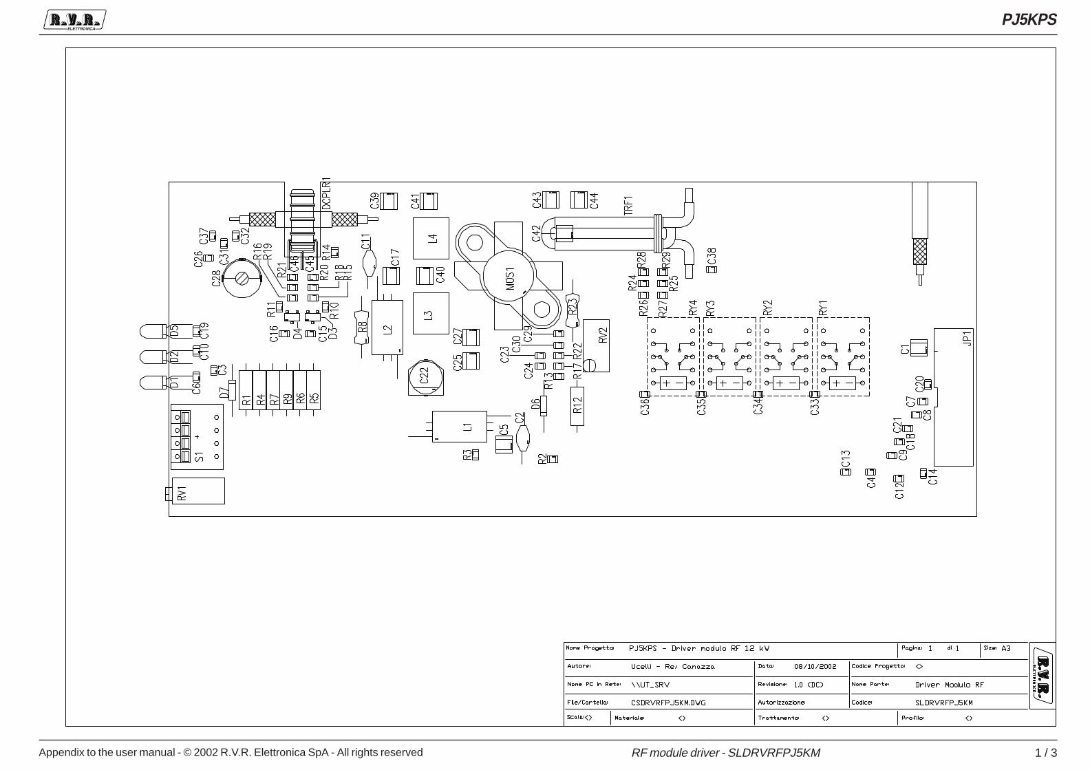
Appendix to the user manual - © 2002 R.V.R. Elettronica SpA - All rights reserved
PJ5KPS
1 / 3RF module driver - SLDRVRFPJ5KM
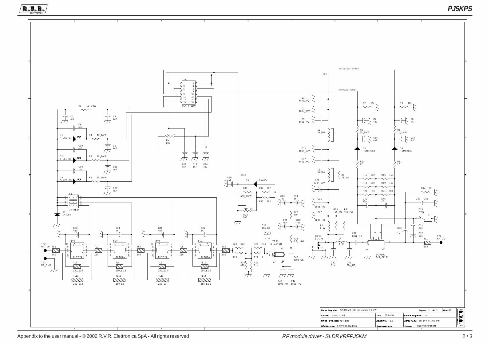
Appendix to the user manual - © 2002 R.V.R. Elettronica SpA - All rights reserved
PJ5KPS
2 / 3RF module driver - SLDRVRFPJ5KM
5
5
4
4
3
3
2
2
1
1
D D
C C
B B
A A
FORWARD POWER
REFLECTED POWER
BIAS
VPA
\ \UT_SRV RF Dr iver 1KW Uni t
C S D R V R F P J 5 K M
1.0
PJ5000MC - Dr iver modulo 1.2 kW
<>
D R I V E R 1 K W . D S N
Mauro Ucel l i 07/06/01
11 A3� � � � � � � � � � � � �
� � � � � � � � � � � � � � � � � � �
� � � � � � � � � � � �
� � � � � � � � � � � � �
� � � � �
� � � � � � � �
� � � � � �
� � � � � � � � � �
� � � � � � � � � � �
� � � � � � � � � ��
C4647p
R27 1
TL14
Z50_E1.5
C40Cxx
TP2RF_INP
C 44n7
cw
R V 120k
C 84n7
TP3R F _ G N D
R28470
C364n7
+-
R Y 2
RLTQ2A
123456
789
10
C4122p_HQ
C 94n7
R29Rxx
TL8
Z50_E1.5
C44680p_HQ
TRF1IN_MATCH
12
3 45TL2
Z50
TL1
Z50
M O S1BLF175
32
1
4
TL12
Z50_E6
C26 Cxx
R 82 2 _ 1 W
D C P L R 1DIR_CPLR
1
2 3
4
7 6 5
C304n7
TP1R F _ O U T
C344n7
D 1R_LED-G3
C3810p_CC
C294n7
R1127C14
4n7
C 64n7
R 2 10k
C39680p_HQ
R1027
R 4 1k_1/4W
R22470
C42270p_CC
+-
R Y 3
RLTQ2A
123456
789
10
D 71N4004
+
C2233uF_63V
TL9
Z50_E1.5
L36 _ W
C 5680p_HQ
TL3
Z50
L4
4 _ W
TL13
Z50_E3
C 2100n_63V
C354n7
C334n7
R21 Rxx
C184n7
R236.8_1/4W
C124n7
R19 150
L1VK200
C43680p_HQ
C 74n7
TL4
Z50
R 51k_1/4W
R16 150
C17680p_HQ
D 3H S M S 2 8 0 0
C 34n7
JP1
FLATT_16PP
1 23 45 67 89 1011 1213 1415 16
R 61k_1/4W
R20 Rxx
D 4H S M S 2 8 0 0
TL6
Z50
R18 150
D 5G_LED-G3
R15 150
R 3 10k
C194n7
cw
R V 2500
C282/20p
31
2
D 6 1N4004
C11100n_63V
C164n7
+-
R Y 1
RLTQ2A
123456
789
10
R 9 1k_1/4W C204n7
C27
680p_HQ
R12
680_1 /4W
C37Cxx
D 2Y_LED-G3
C154n7
C25
680p_HQ
C104n7
TL7
Z50_E1.5
L2VK200
R301k5_2W
TL11
Z50_E12
C214n7
R311k5_2W
C31Cxx
R 7 1k_1/4W
C 1680p_HQ
TL5
Z50
R13 2k2
C32
1p
R17 2k2
S1
76PRB04
1234
8765
R14 1k
R24 Rxx
C244n7
R26 1
+-
R Y 4
RLTQ2A
123456
789
10
R 1 10_1 /4W
C4547p
C234n7
R25 Rxx
TL10
Z50_E1.5
C134n7

Appendix to the user manual - © 2002 R.V.R. Elettronica SpA - All rights reserved
PJ5KPS
3 / 3RF module driver - SLDRVRFPJ5KM
CSDRVRFPJ5KM Bill Of Materials Page1
Item Q.ty Reference Part____________________________________________________________________________________________
1 8 C1,C5,C17,C25,C27,C39, 680p_HQC43,C44
2 2 C11,C2 100n_63V3 24 C3,C4,C6,C7,C8,C9,C10, 4n7
C12,C13,C14,C15,C16,C18,C19,C20,C21,C23,C24,C29,C30,C33,C34,C35,C36
4 1 C22 33uF_63V5 4 C26,C31,C37,C40 Cxx6 1 C28 2/20p
7 1 C32 1p8 1 C38 10p_CC9 1 C41 22p_HQ10 1 C42 270p_CC11 2 C45,C46 47p12 1 DCPLR1 DIR_CPLR13 1 D1 R_LED-G314 1 D2 Y_LED-G315 2 D3,D4 HSMS280016 1 D5 G_LED-G317 2 D7,D6 1N400418 1 JP1 FLATT_16PP
19 2 L2,L1 VK200
20 1 L3 6_W21 1 L4 4_W22 1 MOS1 BLF17523 1 RV1 20k24 1 RV2 1K25 4 RY1,RY2,RY3,RY4 RLTQ2A26 1 R1 10_1/4W27 2 R2,R3 10k28 5 R4,R5,R6,R7,R9 1k_1/4W29 1 R8 22_1W
30 2 R11,R10 2731 1 R12 680_1/4W32 2 R13,R17 2k233 1 R14 1k34 4 R15,R16,R18,R19 15035 5 R20,R21,R24,R25,R29 Rxx36 2 R22,R28 47037 1 R23 6.8_1/4W38 2 R26,R27 139 2 R31,R30 1k5_2W40 1 S1 76PRB0441 6 TL1,TL2,TL3,TL4,TL5,TL6 Z5042 5 TL7,TL8,TL9,TL10,TL14 Z50_E1.543 1 TL11 Z50_E1244 1 TL12 Z50_E645 1 TL13 Z50_E346 1 TP1 RF_OUT47 1 TP2 RF_INP48 1 TP3 RF_GND49 1 TRF1 IN_MATCH

Appendix to the user manual - © 2003 R.V.R. Elettronica SpA - All rights reserved
PJ5KPS
1 / 5RF Module switching power supply - PSSW5040

Appendix to the user manual - © 2003 R.V.R. Elettronica SpA - All rights reserved
PJ5KPS
2 / 5RF Module switching power supply - PSSW5040
SLP.COMP.
ADJ.
50KHZ
VOLTAGE
1V
TP3=1,6V R56=13K3 R57=1K6
INIBIT
PER VOUT 24V R21=3K52 R20=1K0
TP3= 1.6V
\\UT_SRV MAIN BOARD
PSSW5040
1.1 (D.C.)
PJ5KPS - RF module power supply
PJ5000MC_Code
PS5040.DSN
Mauro Ucelli 15/12/03
11 Custom�����������
����� ������������
������ �������
����� ������
���
���������
�����
���������
�������������
������ ������
SS
VOUT
POS
PWM
SS
PWM
VOUT
POS
NEG
VADJ
VADJ
NEG
NEG
VOUT
DG3
VCC
VCC
VCC
VCC
VCC
VCC
VCC
R181M
+C13
EKE1000/63
R41
4K7/2W
C4MKP1nF/600
C27
CM1UF
+
C32
CT1/16
+C11
EKE1000/63
R8
80R2
D13
1N4148
R29
5K62
U1
UC3823
12345678
16151413121109
INV.N.I.E/A OUTCLKRTCTRAMPS.START
VREFVCCOUT
VCPWRGND
ILMREFGND
ILS.D.
R44 NC
JP1
PHOENIX2
12
+C17
EKE1000/63
+
-U5B
LM358
5
67
R32
10R/4W
+C48
EKE470/100
R25
87W-2K
R23
2M7
Q4IRFP250
D14
1N4148
Q2
BC237
F1
BL02
R12
237R
JP13
MOLEX4
1234
JP5
KRA4
1234
F5
FF25A
+
C21EKE1000/63
IS1
4N26
12
54
6
R14
22K/1W
C59CP.1UF
+C14
EKE1000/63
JP4
KRA4
1234
R40 NC
C3
4n7UF2.5%
F3 NC
R212K49
F6
BL02
+C19
EKE1000/63
D11 1N4004
+
C31
CT1/16
Q6IRFP250
+ C1
470uF/40
R50
20K0
D8
LED V
D12
LED V
R11
2K61
R33
10R/4W
R17
1K
R55
180R
+C51
EKE470/100
+C46
EKE470/100
R31
5K62
Q5IRFP250
JP7
KB4
1234
C24
MKP1nF/600
C37CM.1UF
R3647K5
D4
1N4004
+
C8
EKE470/100
+C52
47UF/25
C57
CM.1UF
+C16
EKE1000/63
TP1
TP
R19
87W-500R
C44
MKP-1UF/250
TP4
TP
D1
27V/1W
R60
10K/1W
R54
1K 5%
C28
CM100pF
L9
NC
C42 NC
C36
CM100PF
R15150R
R51
40K2
U2
LM317
3 2
1
VIN VOUT
ADJ
C35CM100PF
U3
LM317
3 2
1
VIN VOUT
ADJ
R12K49
+
C34
EKE1000/63
L10
BFV0710
JP10
MOLEX4
1234
R104820R
R53
20K0
TP3
TP
D7
1N4004
D6
HFA50PA60C
+C22
EKE1000/63
D5
HFA50PA60C
-+
D3
WL02
JP6
NC
12
+C15
EKE1000/63
R3
100R
TP2
TP
L1
BFT0740
C10
MKP-1UF/250
C49
CP.22UFRV1
V120ZA6
R246k81
R5768R 5%
C30CM.1UF
+C47
EKE470/100
R7
237R
R132K61
+
C50
470UF/40
JP3
KRA4
1234
R16392R+
-
U5A
LM358
3
21
84
L5130uH
R28 5K62-V0+
U4
HTM50
1 2
3 54
R10
3K3
R30 5K62
C23
MKP1nF/600
F2 NC
JP11
MOLEX4
1234
C33CP10KPF
L8
NC
R5240K2
R202K0
Q3IRFP250
C41NC
C54
MKP-1UF/250
+
C12EKE1000/63
D2
30V/1W
+
C7
EKE470/100
+ C2
100UF/25
+C60
2.2UF/16
R24K02
C18 NC
T1
15V
JP2
KRA4
1234
JP14
PHOENIX2
12
R351K0
R9
3K3
+C20
EKE1000/63
+
C6
EKE470/100
C40100PF
C55CM
L6130uH
R43
22R/1W
R56
13K3
C43
NC
R59
820R
C29CM1KpF
R105
820R
DL1
LED R
R26
1K0
+C5
EKE470/100
C39100PF
C26CM.1UF
IS2
NC
12
54
6
R4
100R
R27
22K
Q1
50RIA20
F4
FF25A
D10
NC
C53
CP.1UF
C45
NC
C58 100PF
Q7IRFD120
R610R/4W
R22
5K11
JP8
MOLEX4
1234
R58
87W-10K
JP9
MOLEX4
1234
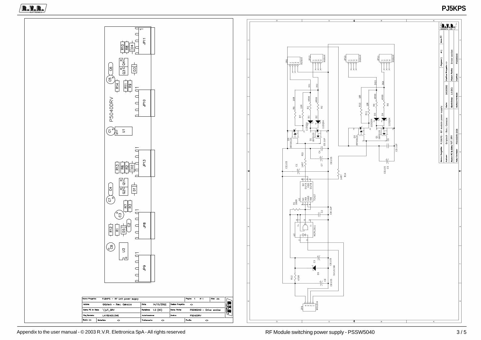
Appendix to the user manual - © 2003 R.V.R. Elettronica SpA - All rights reserved
PJ5KPS
3 / 5RF Module switching power supply - PSSW5040
8 8
7 7
6 6
5 5
4 4
3 3
2 2
1 1
DD
CC
BB
AA
DG1
DG2
PJ
5KP
S -
RF
mo
du
le p
ow
er s
up
ply
<>
1
Gri
ptec
h -
Rev
.: C
anaz
za
Dri
ver
sect
ion
PSSW
5040
\\UT_
SRV
P50
40D
RV.
DSN
14/1
0/20
02
A3
1
1.0
(DC
)
� ���
� ����
�� ��
� ��
��
� �� ��
� ����
�� ��
� ���
�� �
� �� ��
� � �� � ��
� ��� ��
� �� ��
� �� � ����
� �� ���
� ���
� ��� ��
� ��
����
����
� �� ���
� ���
�
DG
3
DG4
R11
10R
R13
14R
7
R14
14R
7
+C
1
CE
1/25
C6
CD
.1U
F
C4
CD
.1U
F
R12
470R
D5
5V1/
0.5W
C2
CM
.1U
F
Q1
IRF
D12
0
2
1
3
+C
3
CE
1/25
+ C8
CE
1/25
JP8
mol
ex4
1 2 3 4
JP13
mol
ex4
1 2 3 4 JP10
mol
ex4
1 2 3 4 JP11
mol
ex4
1 2 3 4
Q3
IRF
D91
20
2
1
3
JP9
MO
LEX
4
1234
Q3
IRF
D91
20
2
1
3
+C
5C
E1/
25
+C
7 CE
1/25
Q1
IRF
D12
0
2
1
3
R1
390R
D1
11D
Q04
D2
11D
Q04
R2
4R99
U1
TC
427
1 2 3 4
8 7 6 5
NC
INA
GN
DIN
B
NC
OU
TA
VD
DO
UT
BR
34R
99
R6
10R
R7
10R
V+
V-
U2
HC
PL2
611
8 57 632
D3
11D
Q04
D4
11D
Q04
R8
4R99
R9
4R99
R10
10R
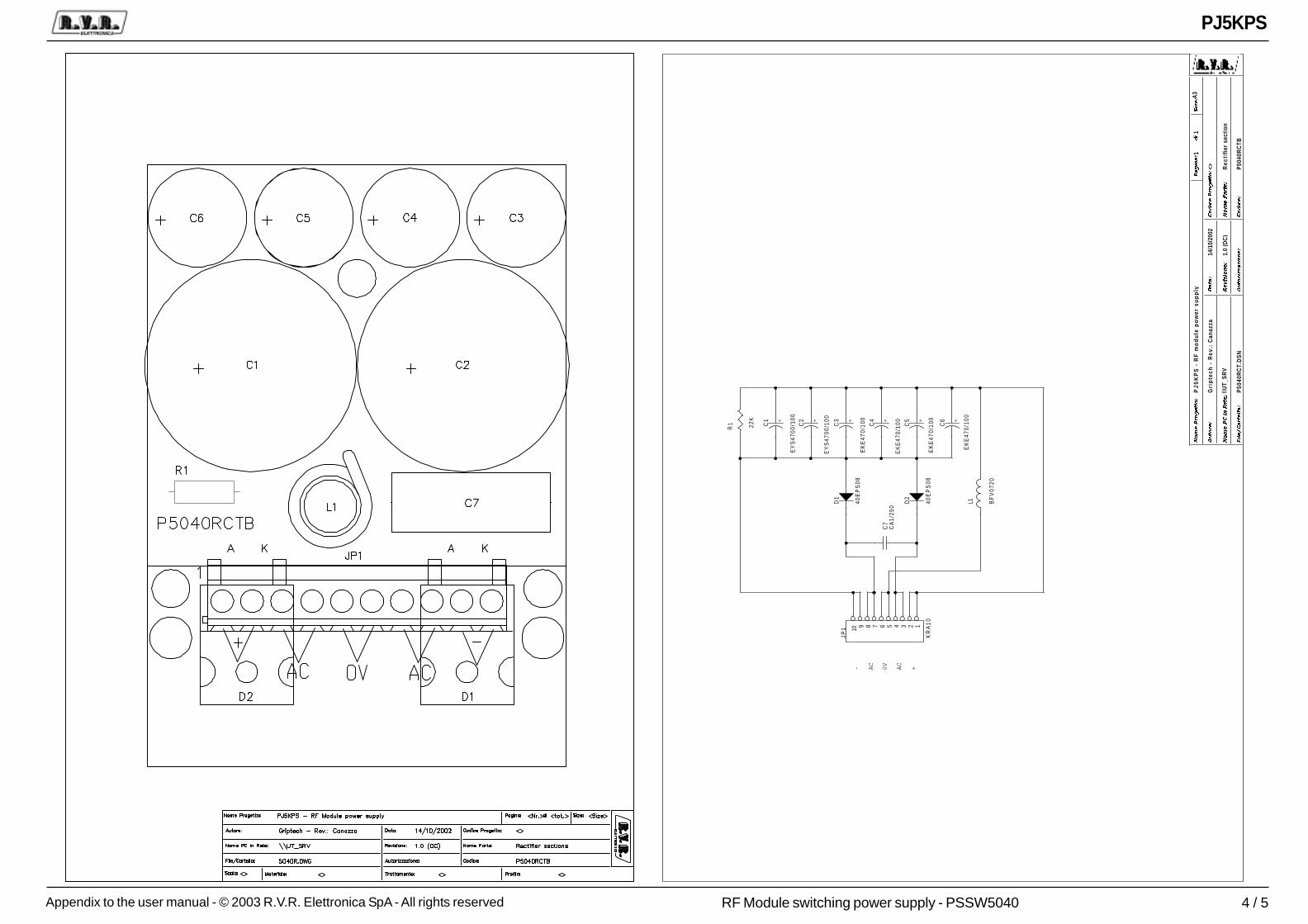
Appendix to the user manual - © 2003 R.V.R. Elettronica SpA - All rights reserved
PJ5KPS
4 / 5RF Module switching power supply - PSSW5040
AC
0V
AC
- +
PJ
5K
PS
- R
F m
od
ule
po
wer
su
pp
ly
<>
1
Gri
pte
ch -
Rev
.: C
anaz
za
Rec
tifi
er s
ecti
on
P504
0RC
TB
\\UT_
SRV
P50
40R
CT.
DSN
14/1
0/20
02
A3
1
1.0
(DC
)
� ���
� ����
�� ��
� ��
��
� �� ��
� ����
�� ��
� ���
�� �
� �� ��
� � �� � ��
� �����
� �� ��
� �� � ����
� �� ���
� ���
� ��� ��
� ��
����
����
� �� ���
� ���
�
JP1
KR
A1
0
12345678910
L1 BF
V07
20
D2
40E
PS
08
D1
40E
PS
08
C7
CA
1/25
0
+
C1
EY
S47
00/1
00 +
C2
EY
S47
00/1
00 +
C3
EK
E47
0/10
0 +
C4
EK
E47
0/10
0 +
C5
EK
E47
0/10
0 +
C6
EK
E47
0/10
0
R1
22K
Appendix to the user manual - © 2003 R.V.R. Elettronica SpA - All rights reserved
PJ5KPS
5 / 5RF Module switching power supply - PSSW5040
PSSW5040 Bill Of Materials Page1
Item Q.ty Reference Part__________________________________________________________________________________________
1 2 Q7, Q1 IRFD1202 4 Q3, Q4, Q5, Q6 IRFP2503 1 Q3 IRFD91204 5 C1,C3,C5,C7,C8 CE1/255 2 C1,C2 EYS4700/1006 2 C1,C50 470UF/407 5 C2,C26,C30,C37,C57 CM.1UF8 1 C2 100UF/259 1 C3 4n7UF10 10 C3,C4,C5,C6,C7,C8,C46, EKE470/100
C47,C48,C5111 2 C6,C4 CD.1UF12 3 C4,C23,C24 MKP1nF/60013 1 C7 CA1/25014 3 C10,C44,C54 MKP-1UF/25015 12 C11,C12,C13,C14,C15,C16, EKE1000/63
C17,C19,C20,C21,C22,C3416 11 IS2,F2,F3,L8,L9,D10,C18, NC
R40,C42,R44,C4517 1 C27 CM1UF18 3 C28,C35,C36 CM100PF19 1 C29 CM1KpF20 2 C32,C31 CT1/1621 1 C33 CP10KPF22 3 C39,C40,C58 100PF23 3 JP6,C41,C43 NC24 1 C49 CP.22UF25 1 C52 47UF/2526 2 C53,C59 CP.1UF27 1 C55 CM28 1 C60 2.2UF/1629 1 DL1 LED R30 2 D2,D1 40EPS0831 1 D1 27V/1W32 4 D1,D2,D3,D4 11DQ0433 1 D2 30V/1W34 1 D3 WL0235 3 D4,D7,D11 1N400436 1 D5 5V1/0.5W37 2 D6,D5 HFA50PA60C38 2 D12,D8 LED V39 2 D14,D13 1N414840 2 F6,F1 BL0241 2 F4,F5 FF25A42 1 IS1 4N2643 1 JP1 KRA1044 2 JP1,JP14 PHOENIX245 4 JP2,JP3,JP4,JP5 KRA446 1 JP7 PHOENIX447 5 JP8,JP9,JP10,JP11,JP13 MOLEX448 1 JP12 JUMPER249 1 L1 BFT074050 1 L1 BFV072051 2 L6,L5 130uH52 1 L10 BFV0710
53 1 Q1 50RIA2054 1 Q2 BC23755 1 RV1 V120ZA656 1 R1 22K57 1 R1 390R58 2 R21,R1 2K4959 1 R2 4K0260 4 R2,R3,R8,R9 4R9961 2 R3,R4 100R62 4 R6,R7,R10,R11 10R63 3 R6,R32,R33 10R/4W64 2 R12,R7 237R65 1 R8 80R266 2 R9,R10 3K367 2 R11,R13 2K6168 1 R12 470R69 2 R13,R14 14R770 1 R14 22K/1W71 1 R15 150R72 1 R16 392R73 1 R17 1K74 1 R18 1M75 1 R19 87W-500R76 1 R20 2K077 1 R22 5K1178 1 R23 2M779 1 R24 6k8180 1 R25 87W-2K81 2 R26,R35 1K082 1 R27 22K83 4 R28,R29,R30,R31 5K6284 1 R36 47K585 1 R41 4K7/2W86 1 R43 22R/1W87 2 R50,R53 20K088 2 R51,R52 40K289 1 R54 1K 5%90 1 R55 180R91 1 R56 13K392 1 R57 68R 5%93 1 R58 87W-10K94 3 R59,R104,R105 820R95 1 R60 10K/1W96 4 TP1,TP2,TP3,TP4 TP97 1 T1 15V98 1 U1 UC382399 1 U1 TC427100 2 U3,U2 LM317101 1 U2 HCPL2611102 1 U4 HTM50103 1 U5 LM358
Related Documents