Nanotechnology PAPER Controlling the number of layers in graphene using the growth pressure To cite this article: Joon Hyong Cho et al 2019 Nanotechnology 30 235602 View the article online for updates and enhancements. This content was downloaded from IP address 146.6.236.81 on 21/04/2019 at 06:27

Welcome message from author
This document is posted to help you gain knowledge. Please leave a comment to let me know what you think about it! Share it to your friends and learn new things together.
Transcript

Nanotechnology
PAPER
Controlling the number of layers in graphene using the growth pressureTo cite this article: Joon Hyong Cho et al 2019 Nanotechnology 30 235602
View the article online for updates and enhancements.
This content was downloaded from IP address 146.6.236.81 on 21/04/2019 at 06:27
Controlling the number of layers in grapheneusing the growth pressure
Joon Hyong Cho1,4 , Seung Ryul Na2,4,5, Saungeun Park3,Deji Akinwande3, Kenneth M Liechti2,5 and Michael A Cullinan1,5
1Department of Mechanical Engineering, The University of Texas at Austin, Austin, TX 78712, UnitedStates of America2Department of Aerospace Engineering and Engineering Mechanics, The University of Texas at Austin,Austin, TX 78712, United States of America3Department of Electrical and Computer Engineering, The University of Texas at Austin, Austin, TX78712, United States of America
E-mail: [email protected], [email protected] and [email protected]
Received 16 December 2018, revised 30 January 2019Accepted for publication 19 February 2019Published 25 March 2019
AbstractMonolayer graphene is commonly grown on Cu substrates due to the self-limiting nature ofgraphene synthesis by chemical vapor deposition (CVD). Consequently, the growth ofmultilayer graphene by CVD has proven to be relatively difficult. This study demonstrates thatthe number of layers in graphene synthesized on a copper substrate can be precisely set bycontrolling the partial pressure of hydrogen gas used in the CVD process. This study also showsthat a pressure threshold exists for a distinct transition from monolayer to multilayer graphenegrowth. This threshold is shown to be the boundary where the graphene growth process on Cu byCVD is no longer a self-limiting process. In addition, the multilayer graphene synthesizedthrough the pressure control method forms in the Volmer–Weber mode with an AB stackingstructure.
Supplementary material for this article is available online
Keywords: multilayer graphene, chemical vapor deposition, graphene electronics
1. Introduction
Bilayer and multilayer graphene have found many uses in arange of applications from low resistance flexible transparentelectrodes [1] to corrosion protection [2, 3] to roll-to-rollelectronics manufacturing [4–6]. For example, bilayer gra-phene has a tunable bandgap [7] and is ideal for tunnel fieldeffect transistors [8, 9]. However, the precise fabrication ofbilayer or multilayer graphene with a controlled number oflayers is extremely difficult. Most attempts to produce bilayeror multilayer electronic devices have relied on the attemptingto find sections of bilayer/multilayer graphene on samplesexfoliated from bulk graphite samples [10–13]. The resultsfrom these devices are encouraging with a band-gap up to0.25 eV demonstrated for bi-layer graphene produced by this
mechanical exfoliation method [7]. However, this method isnot scalable to the large-scale production needed for elec-tronics manufacturing. Therefore, various studies attempted toproduce bi- or multi-layer graphene with an AB laminationstructure using chemical vapor deposition (CVD), which is amore scalable graphene fabrication method.
Unfortunately, the controlled fabrication of bilayer ormultilayer graphene by CVD has proven to be difficult. MostCVD graphene is grown on copper substrates because of theself-limiting nature of graphene growth on copper [14]. InCVD graphene grown on copper, the copper surface thatserves as the catalyst for graphene synthesis becomes coveredwith the graphene which prevents the copper from catalyzingmore graphene growth and thus inhibiting multilayer gra-phene growth [15]. One approach to overcome this challengehas been to grow graphene on Cu–Ni alloys [16, 17]. Thepresence of Ni in the Cu–Ni alloy helps to increase the carbonsolubility in the alloy and thus promotes multilayer growth.
Nanotechnology
Nanotechnology 30 (2019) 235602 (10pp) https://doi.org/10.1088/1361-6528/ab0847
4 These authors contributed equally to this work.5 Authors to whom any correspondence should be addressed.
0957-4484/19/235602+10$33.00 © 2019 IOP Publishing Ltd Printed in the UK1

However, the increased carbon solubility makes growinguniform graphene on these Cu–Ni alloys difficult, whichgenerally results in large variances in the number of layersacross the sample grown using this method [17, 18].
Recent research has reported that it is possible to syn-thesize multi-layer graphene by either changing the carbon tohydrogen ratio or increasing the partial pressure of hydrogenduring the CVD growth process [19, 20]. Liu [21] hasreported the successful synthesis of multilayer graphene bycontrolling the hydrogen partial pressure while supplyinghydrogen and methane. Luo also reported that multilayergraphene can be synthesized through dynamic control ofpressure in the process of graphene synthesis [22]. However,the ability to precisely control the growth of bilayer or few-layer graphene with a set number of layers has yet to bedemonstrated or analyzed. Therefore, the purpose of thisstudy is to quantify the effect that the hydrogen partial pres-sure has on the growth of bilayer and multilayer graphene inorder to understand the role of pressure in multilayer gra-phene growth and to be able to precisely grow bilayer or few-layer graphene.
2. Experimental section
This section outlines how the graphene was grown on copperfoil and how it was transferred to the SiO2 surface of a siliconchip for characterization.
2.1. Graphene growth on copper foils
In this work, the graphene growth was performed with oncopper foils (thickness of 130 μm and purity of 99.95%, AlfaAesar) as the metal catalyst. The Cu foil was 1×6 inchesand was chemically treated in a 0.1 M ammonium persulfatesolution (APS) for 30 min to remove the layer of nativecopper oxide as well as other contaminations that exist on thecopper foil. This was followed by sequentially cleaning thecopper in acetone, isopropyl alcohol (IPA), and de-ionized(DI) water bath. The treated copper foil was placed in themiddle of a quartz tube in the growth furnace. Graphenegrowth was then preformed according to the following steps:(1) the pressure in the quartz tube was pumped down to10 mTorr, (2) the copper foil was heated to 1030 °C under aflow of hydrogen gas of 10 standard cubic centimeters perminute (SCCM) in the quartz tube; (3) the specific pressurefor graphene-growth was set by controlling the down flowvalve of the CVD system under a constant temperature(1030 °C) and hydrogen environment (pressures of 0.47, 10,40, 50, 80, and 120 Torr were selected for the multilayergraphene growth); (4) graphene growth was then conductedwith two mixtures of hydrogen and methane at 10 SCCMand 0.1 SCCM for 30 min at 1030 °C, respectively; (4) theentire CVD system was naturally cooled while flowing thegas mixtures and the coated copper foil was removed foranalysis. (For details, see figure S1 in supplementaryinformation, available online at stacks.iop.org/NANO/30/235602/mmedia.)
2.2. Transfer of graphene to silicon oxide substrates andelectrical measurements
In order to evaluate the properties of graphene, as-growngraphene on the copper foil was transferred to 300 nm thicksilicon oxide substrates on silicon, SiO2/Si (100), by thetypical poly(methyl methacrylate) (PMMA) assisted wettransfer technique. The PMMA (100 K molecular weight,Microchem) was spin-coated on the graphene on the copperfoil at the rate of 4000 RPM for 45 s. After pre-curing thePMMA/graphene/Cu foil/graphene composite at 190 °C for20 min, the graphene without PMMA beneath copper foil wasetched by exposing it to an O2 plasma environment [23] for10 s. The sample was then placed in an APS solution of 0.1 Mfor 10 h to etch away the copper foil and leave behindPMMA/graphene floating on top of the APS solution. Thethin PMMA/graphene film was cleaned in DI water and thentransferred onto SiO2/Si substrates and stored in a vacuumdesiccator to remove trapped water between PMMA/gra-phene and the substrate. After drying the sample overnight,stronger adhesion between graphene and the substrate wasachieved by baking the sample at 120 °C for 15 min. Finally,graphene-coated silicon was obtained by removal of thePMMA layer in an acetone bath for 60 min, followed byannealing under ambient conditions at 450 °C for 30 min inorder to remove any of the remaining polymer residue on thesample [24]. For the electrical measurements of the graphene,Au/Cr electrodes with 4 different gap sizes of 25, 50, 100,and 200 μm were deposited on top of the graphene.
3. Results and discussion
Monolayer, bilayer and multilayer of graphene (three or morelayers) were synthesized on the copper foil by the CVDprocess described above. Figure 1 shows a series of scanningelectron microscope (SEM) images of as-grown graphene oncopper foil at 0.47, 10, 40, 50, 80 and 120 Torr (seefigures 1(a)–(f)), respectively (For larger scale SEM images,see figure S3 in supplementary information.)
As can be seen in figure 1, graphene grown at a pressureof 0.47 Torr (figure 1(a)) is a wrinkle free monolayer gra-phene whereas wrinkles are present under the higher-pressuregrowth conditions, indicating the presence of multilayergraphene. Only copper steps are visible on the graphene onCu foil in figure 1(a). Though the origin of wrinkles inmultilayer graphene is not well known [25, 26], it is hypo-thesized that the wrinkles (ML wrinkle in figures 1(b)–(f)represented as white lines in SEM) in the multilayer graphenemost likely result from the formation of vacancies betweenlayers in the graphene. As a result of the difference of theemissivity resulting from the vacancies between interlayers,these wrinkles appear as the bright lines in the SEM images[25, 27, 28]. These ML graphene wrinkles are distinguishablefrom monolayer graphene wrinkles because monolayer gra-phene wrinkles are darker in contrast. In addition, it can beobserved in figure 1 that as the growth pressure increases, theoverall contrast on the graphene in the images becomes darker
2
Nanotechnology 30 (2019) 235602 J H Cho et al

Figure 1. SEM of graphene grown on the copper foil at: (a) 0.47, (b) 10, (c) 40, (d) 50, (e) 80, and (f) 120 Torr where ML is an abbreviationfor multilayer. The scale bar (red line at the bottom right corner) indicates 5 μm.
Figure 2. Raman responses of graphene on copper foil: Raman mapping of I2D/IG of (a) 0.47, (b) 10, (c) 50, (d) 80, (e) 120 Torr, and (f)Raman spectra of four selected regions of graphene at 0.47 Torr. The Raman mappings were conducted on an area of 10×10 μm. TheRaman spectra of other cases (10–120 Torr) are given in the supplementary information figure S4.
3
Nanotechnology 30 (2019) 235602 J H Cho et al

which further indicates that the number of graphene layers isincreasing [29, 30].
To characterize the quality and number of layers of as-grown graphene on the copper foil, Raman spectroscopy(WITec Alpha 300 micro-Raman confocal microscope,λ=488 nm) was conducted on the copper foil after graphenegrowth. Figures 2(a)–(e) are the images of the Raman map-ping associated with the intensity ratio (I2D/IG) of G and 2Dpeak at growth pressures of 0.47, 10, 50, 80, and 120 Torr,respectively. In these Raman images, blue regions indicate thepresence of bi-layer graphene and purple regions indicatemultilayer graphene while the red and yellow-colored regionsare monolayer graphene.
The Raman spectrum mapping image (see figure 2(a)) at0.47 Torr shows that the entire surface was covered withmonolayer graphene as evidenced by the fact that the intensityratio between the 2D and the G peaks of Raman spectra(I2D/IG) is greater than two over the majority of the surface[17]. For the 10 Torr growth (figure 2(b)) shows that mono-layer graphene is still dominant over the entire surface butthat small spots of bi-layer graphene (see supplementaryinformation in figure S4(a)) for the details of selected regions)are observable. In graphene growth with a pressure exceeding10 Torr, the percentage of monolayer graphene starts to droprapidly as increasing areas of bilayer and multilayer grapheneare formed. At 50 Torr (see figure 2(c)), only about 20% ofthe scanned area of the mapping was covered with monolayergraphene and the rest of the area was bi-layer (I2D/IG∼1)and multilayer (I2D/IG<1) as represented by the blue andpurple domains, respectively. Further details of Ramanspectra in the blue and purple regions are analyzed in figureS4(b). For the 80 Torr (see figure 2(d)) and 120 Torr (seefigure 2(e)) cases, bi-layer or multilayer graphene covers mostof the surface. (For the details of 80 and 120 Torr at theselected regions please see figures S4(c), (d) in supplementaryinformation, respectively.) These Raman spectra results sup-port the conclusion based on the contrast and presence of the
wrinkles in SEM (see figure 1) that the number of graphenelayers increases as the growth pressure increases.
Quantifying the effect of the growth pressure on thenumber of layers is important, therefore, we analyzed prob-ability distribution functions of the I2D/IG intensity ratioscalculated by examining each of the large area Raman scansfor the different pressure growths on a pixel-by-pixel level asshown in figure 3(a). In general, as the pressure increases, theprobability distribution function becomes broader indicating awider range in the number of graphene layers present in thesamples. These probability distributions were then used tocalculate the percentage of monolayer, bilayer, and multilayergraphene in the growths as a function of the growth pressureas shown in figure 3(b). In this figure, the average ofpercentage of number of layers was determined by calculatingaccumulation of area under the curve where the area under thecurve of I2D/IG range from 1.5 to 3.0 is considered mono-layer, the range from 0.8 to 1.5 is considered bilayer, andbelow 0.8 is considered multilayer graphene. The error bars infigure 3(b) were calculated as the standard deviation of thelayer number percentages between different Raman scans forgrowths with the given growth pressure.
As can be seen in figure 3(b), the percentage of mono-layer graphene decreases as growth pressure is increased andthe percentage of multilayer increases. The percentage ofbilayer graphene is highest at the growth pressure of 50 Torrand more multilayer graphene starts being produced at higherpressures. This graph clearly shows that the amount of mul-tilayer graphene rises with increasing growth pressure.
Raman spectroscopy is a convenient tool for determiningnumber of graphene layers on Cu foil or on SiO2/Si substrate;however, the Raman responses on multilayer graphenebecome ambiguous when the number of graphene layers isgreater than three. For example, when the Raman response ofI2D/IG ratio on graphene is below 0.75 (as is the case withgrowth pressures above 80 Torr), it is difficult to accuratelyevaluate the number of graphene layers since the more
Figure 3. (a) Raman response of graphene as normalized distributions of I2D/IG. (b) The percentage of the number of layers as a function ofgrowth pressure of which graphene was grown. The average percentage of the number of layers and associated error bars were analyzed fromRaman intensity data in figure 3(a) by accumulating the area under the curve.
4
Nanotechnology 30 (2019) 235602 J H Cho et al

graphene layers do not significantly affect the I2D/IG ratio.Thus, for precise measurement of the number of layers in themultilayer graphene grown in this study, atomic forcemicroscopy (AFM, Park Scientific XE-100) was used. Whileobtaining morphology data from AFM, we also measured thelateral force spectrum of the surface, which helped us tovisualize copper morphology as well as graphene steps.
The AFM image in figure 4(a) shows the morphology ofa typical monolayer graphene/Cu foil surface grown at apressure of 0.47 Torr over a 5×5 μm area. The scannedregions are characterized by the hexagonal graphene domains(average radius is approximately 0.6 μm, see figures S8, 9 insupplementary information). The size of Cu grains in thesefoils were determined to be larger than 10 μm by SEM byobservation in figure 1, therefore the hexagonal patterns in theAFM images are graphene grains [31]. In order to make surethat the hexagonal patterns are indeed graphene grainboundaries, a closer-up scan (see figure 4(b)) of the whiterectangle in figure 4(a) is shown in which the details ofcopper steps in the hexagonal pattern are observable. Thehexagonal patterns are also observed to be surrounded byragged lines which are copper oxide formed at the defects atthe interfaces of the of as-grown graphene grains.
AFM scans (see figure 4(c)) of graphene synthesized oncopper foil at 120 Torr show that the hexagonal pattern grew
radially and repeated for the multilayer graphene samples. Ifgraphene layers are formed, the thickness difference at eachstep should be approximately 0.335 nm [32]. Figure 4(d)shows a line profile of height indicated in figure 4(c) as Lineprofile 1 on Copper (L1). Each step represents a graphene stepcounting from graphene ‘1’ to graphene ‘5’. Each step heightdifference from the measurement is calculated by subtractinga morphology of copper surface from original AFM data asshown in figure 4(e) where average height difference fromstep to step is approximately 0.4 nm. Region 4–5 has heightdifference of 2 layers of graphene stacked which is calculatedas 0.8 nm. Therefore, figure 4(e) suggests that approximatelysix layers of graphene were formed at the selected location ongraphene.
In order to understand how the multilayer graphenegrains grow and coalesce, graphene was produced by short-ening the growth time. Total absorption time of 10 mininstead of the original recipe of 30 min was used. Graphenegrown on Cu foil in this manner under 120 Torr is shown infigures 5(a), (b) where a few graphene grains are producedbefore fully covering the surface of Cu foil.
Figure 5(a) exhibits a patch of multi-layer graphene,contacting with an adjacent region of multi-layer graphene. Inaddition, we can observe multilayer wrinkles (ML wrinkle) atthe center of each graphene domain as well as where they
Figure 4.AFM image of graphene grown on copper foil: (a) graphene at 0.47 Torr, (b) high resolution image near copper oxide and graphenegrains, (c) graphene at 120 Torr, (d) height profile of the graphene steps along the line L1, and (e) the height difference between each region.
5
Nanotechnology 30 (2019) 235602 J H Cho et al

merge. This is clear in figure 5(b), with the formation of aboundary (a white arrow) of multi-layer graphene grains (A–D) with several wrinkles in each domain. Figure 5(c) showsthat the I2D/IG ratio of two nearby graphene patches variesfrom 0.3 to 0.8. This mapping image shows that when thegraphene was formed on copper, the monolayer and bilayergraphene grew outward from the nucleation point andsimultaneously formed more layers of graphene at thenucleation point. The white circles (see figure 5(c)) representthe locations (1–7) where the Raman spectra were observedon the sample. In figure 5(c), location 1 is the center ofmultilayer graphene which corresponds to the Raman spec-trum labeled ‘1’ in figure 5(d) with an I2D/IG ratio of 0.7. Dueto the decrease of the ratio (I2D/IG) from point 2 to point 3,we estimated that tri and bi-layer graphene were formed atthese points, respectively. The absence of the two character-istic peaks of graphene (point 4) supports the absence of thegraphene layer on copper there. Along the points 5, 6, and 7,the Raman spectra indicate that bi-layer, tri-layer and fewlayers of graphene were formed, respectively. The FWHM ofI2D of graphene shown in figure 5(e) indicates that themajority of FWHM is close to 60, indicating AB stacking ofgraphene layers [33]. Thus, it is possible to conclude that themultilayer graphene grown on the copper was AB stackedgraphene in each domain. When the growth process describedabove was repeated at 80 Torr, similar graphene growth pat-terns were observed (see figure 5(f)). These results indicatethat the growth of the multi-layer graphene proceeds from thenucleation sites until the graphene patches merge together.
To accurately quantify the number of graphene layersthat form in the multilayer domains, the multilayer graphenewas transferred onto a silicon oxide surface and atomic forcemicroscopy was used to measure the number of layers acrossmultiple locations on the sample. The SEM image infigure 6(a) shows graphene grown at 120 Torr consisting ofmultilayers having visibly different contrast due to differentnumbers of layers of graphene at different regions in thesample. Multilayer graphene is also confirmed by the AFMmapping data in figure 6(b), where the hexagonal domains aredefined by steps, multi-layer graphene wrinkles, and grainboundaries. When the height profile along L2 (see figure 6(c))was measured along with the friction at each step using lateralforce microscopy (LFM), it suggests that multilayer graphenegrowth is most likely to be stacked in the form of Volmer–Weber (VW) type graphene structures, in which additivelayers are formed beneath monolayer graphene [20, 34], sincethere was no change in the measured friction at each step. Theresults are consistent with the expected growth mechanismgiven the low methane concentration ratio growth conditionsused and the stacking sequence visible in figures 6(a), (b). Inaddition, the height variation at each step (see figure 6(d))suggests that average graphene step heights of 0.38 nm aredistinguishable within ±0.1 μm. Height measurements ofvarious wrinkles and boundary layers of graphene grains arepresented in figures S8(a), (b) in supplementary information.The Raman spectra of the transferred graphene is shown infigure 6(e) where the ratio of peak intensities I2D/IG ismapped for the sample. The mapping shows that the majority
Figure 5. A demonstration of graphene growth: (a) SEM image of growth at 120 Torr, (b) SEM image at different locations, (c) Ramanmapping (I2D/IG) of partially grown graphene on copper foil, (d) Raman spectra from point 1 to point 7, (e) the plot of FWHM, and (f) SEMimage of partially grown graphene at 80 Torr.
6
Nanotechnology 30 (2019) 235602 J H Cho et al

of 10×10 μm area is covered with multilayer graphene(I2D/IG≈0.5) and that the boundaries of the graphene pat-ches are close to bilayer graphene (I2D/IG≈1).
Statistical values gathered from both the Raman data infigure 3(a) and the AFM data (by counting the actual numberof graphene layers in the transferred multilayer samples) wereused to estimate the average number of layers and the possiblerange in the number of layers at each growth pressure.
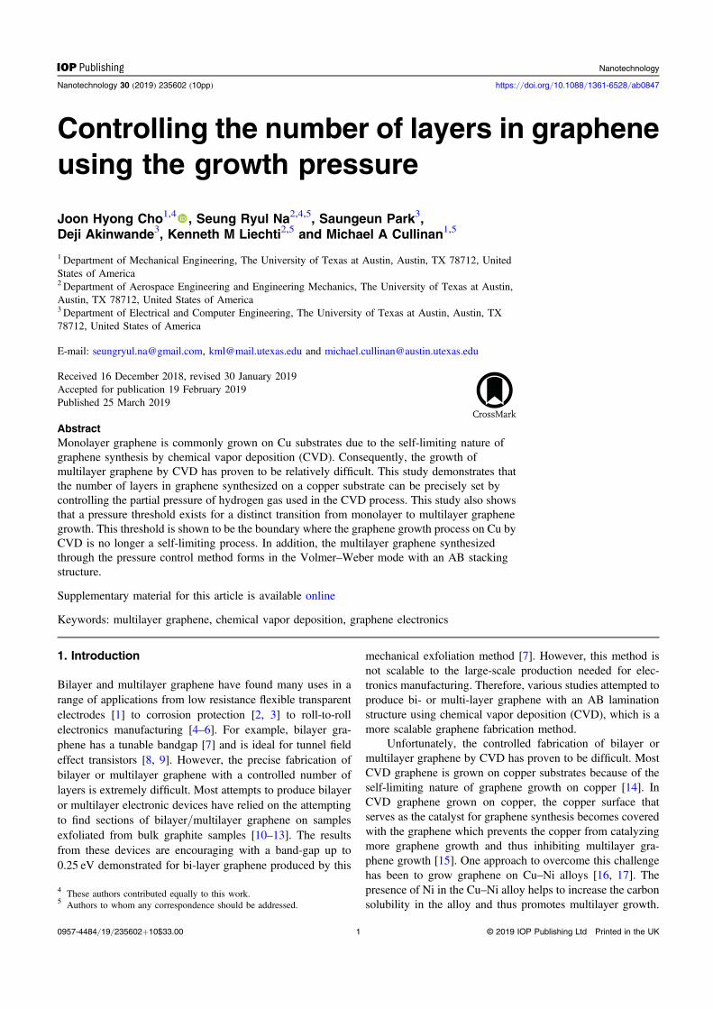
Figure 7(a) shows number of graphene layers measuredat the center of graphene grains as a function of the growthpressure in box chart where the top quarter and the bottomquarter of percentiles are represented by the rectangularboxes. The average value of each growth is marked as a linein the boxes. As can be seen in figure 7(a), the averagenumber of graphene layers increases as the growth pressureincreases and that the range in the number of layers foundalso increases as the pressure increases.
For growth pressures below 10 Torr, most of the gra-phene grown is monolayer but above 10 Torr the growthconditions start to exhibit an increased variation in the num-ber of layers grown. A growth pressure of approximately40 Torr appears to be the point where bilayer graphene startsto become the dominant graphene configuration. At 50 Torr,more multilayer graphene starts to grow so that while theaverage number of graphene layers remains at 2–3 layers.Overall, it is observed that, as as the pressure increases, there
are small sections of the sample that contain far more than theaverage number of layers for that growth pressure. Forexample, when grown at 80 Torr, there can be up to 7 gra-phene layers while the average number of layers is only 4–5and at 120 Torr, up to 11 layers were observed sporadicallywhereas the average number of layers is only 8. These spotsof high layer counts show that new layers can quickly form atnucleation sites for the high-pressure growths when the gra-phene growth is no longer self-limiting.
It has been well-reported that the graphene growth atlower pressures is a self-limiting process, leading the forma-tion of monolayer graphene on copper foil [15]. However,controlling the partial pressure of hydrogen prior to supplyingmethane shows that the self-limiting process can overcome,thereby enabling multilayer graphene growth on the surfaceof Cu foil. This study shows that growth pressures from 10 to40 Torr are the threshold of the self-limiting process, and thatmultilayer graphene starts to grow above this threshold. Thisbreakdown in the self-limiting nature of the growth process ismost likely due to a change in the rate limiting step of theprocess occurring at this pressure. Two fluxes can occur atsimultaneously in the CVD process; mass-transport throughthe boundary layer and surface-reaction transport through thesurface layer as shown in equations (1)–(3) where hg is masstransport coefficient, Ks the surface reaction constant, Cg isthe concentration of gas in the bulk, and Cs is the
Figure 6. Diagnostics of the wet-transferred graphene on silicon oxide: (a) SEM image of the transferred graphene, (b) AFM image,(c) profile of graphene steps along line (L2), (d) height difference of graphene steps, and (e) Raman mapping (I2D/IG) of the graphene on anarea of 10×10 μm.
7
Nanotechnology 30 (2019) 235602 J H Cho et al
concentration of the active species at the surface [35]
= -( ) ( )‐F h C C , 1g g smass transport
= ( )‐F K C , 2s ssurface transport
=+
( )‐F CK h
K h. 3g
s g
s gtotal flux
In CVD growth under low pressures, the surface trans-port reaction is the rate limiting step µ( )h K h D,g s g g
since diffusivity through the boundary layer (Dg) formed ontop of the catalyst substrate is inversely proportional to thegrowth pressure due to fewer collisions between moleculesoccurring within this boundary layer at lower pressures.Therefore, at low pressures, the graphene CVD growth pro-cess becomes limited by the surface transport mechanism,resulting in in the growth of monolayer graphene [35]. Forgrowth processes closer to atmospheric pressure, masstransport through the boundary layer is the limiting rate step
( )K h .s g Therefore, non-uniformities in the thickness ofthe boundary layer in the growth region can create changes inthe uniformity of graphene layer and increase the number ofactive species that can diffuse into the surface and lead to the
growth of additional graphene layers. The graphene growthconditions presented in this paper have a pressure range frommTorr to hundreds of Torr, which covers the low-pressureregion where surface transport is the rate limiting step to theatmospheric region where mass-transport is the rate limitingstep. The mass-transport and surface-transport growthmechanisms can co-exist in the transition (10–40 Torr). Themixture of these two growth regimes results in primarilybilayer graphene growth. Therefore, in this growth system,the pressure around 10–40 Torr defines the boundary betweenthe two growth mechanisms well and where the self-limitinggrowth process that results in monolayer graphene growth atlower pressures starts to breakdown.
In order to determine how new multilayer structures areformed as the pressure increases and confirm the cause of thebreakdown of the self-limiting growth process, the full-widthat half maximum (FWHM) of the 2D peaks in each case wasmeasured in order to determine the stacking order of graphenelayers since it has been observed that AB stacking results insignificant 2D peak broadening as compared with AAstacking [33]. Figure 7(b) shows FWHM of monolayer at
Figure 7. (a) Number of graphene layers as a function of the growth pressure in a box chart with average values of each growth conditionmarked as lines in the boxes. (b) Full-width at half maximum shown for each growth. (c) Measured sheet resistance of graphene transferredonto SiO2/Si after growths from each growth pressure. Multilayer graphene exhibits reduced sheet resistance.
8
Nanotechnology 30 (2019) 235602 J H Cho et al

0.47 and 10 Torr was approximately 26 cm−1, 27 cm−1,respectively, suggesting that graphene synthesized on thecopper foil is monolayer graphene. Large variations in thenumber of graphene layers occur when graphene is grown atpressures of 40 and 50 Torr. Depending on the location of themeasurements, FWHM varied from 14 to 47 cm−1 with40 Torr growths and 20 to 40 cm−1 with 50 Torr growths.Graphene growth this region is relatively sensitive to thegrowth pressure causing a large variation in the number ofgraphene layers that are formed. We believe that the thresholdfor breaking the self-limiting process occurs within thisgrowth pressure range. The values of FWHM of the multi-layer graphene was 50 cm−1 and 52 cm−1 at 80 Torr and120 Torr, respectively, which indicates that the stacking orderof the multilayer graphene is AB stacking. This is consistentwith what would be expected under VW growth. Such resultsare reasonable since AB stacking is a more stable stackingorder than the AA stacked graphene configuration [20]. (Forfurther details of FWHM, please see figure S5 in supple-mentary information.) Therefore, as new layers are nucleatedduring the graphene growth process at higher pressures, stableAB stacking layers are formed with the graphene alreadypresent in the sample.
Finally, the sheet resistance as a function of the growthpressure was also measured as shown in figure 7(c). Theseresults show that, as the growth pressure increases, there is areduction in the sheet resistances of the samples, which islikely caused by the increased number of graphene layers inthe samples [4]. This result confirms the results from theAFM/LFM and SEM measurements. However, the resultsalso show that the change in sheet resistance is not a linearfunction of the average number of layers in the graphene. Thisis likely because the secondary layers of graphene grownbelow the primary graphene layer have not fully coalescedinto a complete and uniform layer. Therefore, even though thesample might by >80% bilayer graphene, if the grains of thesecond graphene layer are not completely connected to eachother, then the contact resistance between the grains on thatlayer might be so high that the second layer does not make asignificant contribution to the overall electrical conductivityof the graphene structure [36]. This is supported by the factthat the electrical resistance does not start to drop until thepressure is >40 Torr which is when all of the measured spotson the graphene structure have at least two complete layers.Therefore, as the pressure increases above 40 Torr we wouldexpect to see more complete layers forming and the sheetresistance to start to drop rapidly as is observed in figure 7(c).
Even though not all of the layers in the graphene mighthave fully coalesced, the electrical performance of the gra-phene produced using this growth method are still very good.The measured sheet resistance for the multilayer graphene isless than 100Ω/sq. and the hole mobility of the graphenegrown at 80 Torr, measured using a backgated FET with adrain voltage of 10 mV, is 412–643 cm2 v−1 s−1. Theseresults are consistent with the results for other graphenesamples in the literature that are measured at room temper-ature and atmospheric pressure [4, 21, 37]. (See supplemen-tary information figure S10 for more details.)
4. Conclusions
This paper shows that the number of graphene layers can becontrolled by the pressure during growth. It demonstrates thesuccessful growth of monolayer graphene at pressures below10 Torr and up to 11 layers of graphene at pressures of120 Torr. In addition, the multilayer graphene grows in an ABstacked sequence. A threshold of 10–40 Torr has also beenidentified for breaking the self-limiting process of graphenegrowth on Cu foil that typically results in only monolayergrowth on graphene. There is also a threshold in the40–80 Torr range where majority of the graphene grownchanges from bilayer to multilayer. This threshold was alsoconfirmed by the FWHM of the I2D peak, where graphenegrown at a pressure above 80 Torr has a FWHM of50–60 cm−1, whereas the FWHM is only 20–30 cm−1 atpressures below 50 Torr. Therefore, this work shows that bysetting the pressure during the growth of graphene on coppersubstrates it is possible break the self-limiting growth mech-anism and control the number of graphene layers that aregrown.
Acknowledgments
This work is based upon work supported by the NationalScience Foundation under Cooperative Agreement No. EEC-1160494. We would like thank Dr Piner for AFM/LFMmeasurements and helpful discussions on multilayer graphenegrowth.
ORCID iDs
Joon Hyong Cho https://orcid.org/0000-0002-7329-2556
References
[1] Kim K S, Zhao Y, Jang H, Lee S Y, Kim J M, Kim K S,Ahn J-H, Kim P, Choi J-Y and Hong B H 2009 Large-scalepattern growth of graphene films for stretchable transparentelectrodes Nature 457 706
[2] Chen S et al 2011 Oxidation resistance of graphene-coated Cuand Cu/Ni alloy ACS Nano 5 1321–7
[3] Zhang Y H et al 2014 The distribution of wrinkles and theireffects on the oxidation resistance of chemical vapordeposition graphene Carbon 70 81
[4] Bae S et al 2010 Roll-to-roll production of 30-inch graphenefilms for transparent electrodes Nat. Nanotechnol. 5 574
[5] Gao L, Ni G-X, Liu Y, Liu B, Castro Neto A H and Loh K P2013 Face-to-face transfer of wafer-scale graphene filmsNature 505 190
[6] Naghdi S, Rhee K Y and Park S J 2018 A catalytic, catalyst-free, and roll-to-roll production of graphene via chemicalvapor deposition: low temperature growth Carbon 127 1–12
[7] Ohta T, Bostwick A, Seyller T, Horn K and Rotenberg E 2006Controlling the electronic structure of bilayer grapheneScience 313 951–4
9
Nanotechnology 30 (2019) 235602 J H Cho et al

[8] Das A et al 2008 Monitoring dopants by raman scattering in anelectrochemically top-gated graphene transistor Nat.Nanotechnol. 3 210
[9] Luo G, Zhang Z Z, Deng G W, Li H O, Cao G, Xiao M,Guo G C and Guo G P 2017 Coupling graphenenanomechanical motion to a single-electron transistorNanoscale 9 5608–14
[10] Bunch J S, van der Zande A M, Verbridge S S, Frank I W,Tanenbaum D M, Parpia J M, Craighead H G andMcEuen P L 2007 Electromechanical resonators fromgraphene sheets Science 315 490
[11] Oostinga J B, Heersche H B, Liu X, Morpurgo A F andVandersypen L M K 2007 Gate-induced insulating state inbilayer graphene devices Nat. Mater. 7 151
[12] Xia F, Farmer D B, Lin Y-m and Avouris P 2010 Graphenefield-effect transistors with high On/Off current ratio andlarge transport band gap at room temperature Nano Lett. 10715–8
[13] Meric I, Han M Y, Young A F, Ozyilmaz B, Kim P andShepard K L 2008 Current saturation in zero-bandgap, top-gated graphene field-effect transistors Nat. Nanotechnol. 3 654
[14] Li X, Cai W, Colombo L and Ruoff R S 2009 Evolution ofgraphene growth on Ni and Cu by carbon isotope labelingNano Lett. 9 4268–72
[15] Lin H-C, Chen Y-Z, Wang Y-C and Chueh Y-L 2015 Theessential role of Cu vapor for the self-limit graphene via theCu catalytic CVD method J. Phys. Chem. C 119 6835–42
[16] Pollard A J et al 2009 Formation of monolayer graphene byannealing sacrificial nickel thin films J. Phys. Chem. C 11316565–7
[17] Cho J H, Gorman J J, Na S R and Cullinan M 2017 Growth ofmonolayer graphene on nanoscale copper-nickel alloy thinfilms Carbon 15 441–8
[18] Chen S, Cai W, Piner R D, Suk J W, Wu Y, Ren Y, Kang J andRuoff R S 2011 Synthesis and characterization of large-areagraphene and graphite films on commercial Cu–Ni alloyfoils Nano Lett. 11 3519–25
[19] Yao Y, Li Z, Lin Z, Moon K-S, Agar J and Wong C 2011Controlled growth of multilayer, few-layer, and single-layergraphene on metal substrates J. Phys. Chem. C 115 5232–8
[20] Ta H Q, Perello D J, Duong D L, Han G H, Gorantla S,Nguyen V L, Bachmatiuk A, Rotkin S V, Lee Y H andRümmeli M H 2016 Stranski–Krastanov and Volmer–Webercvd growth regimes to control the stacking order in bilayergraphene Nano Lett. 16 6403–10
[21] Liu Q, Gong Y, Wilt J S, Sakidja R and Wu J 2015Synchronous growth of AB-stacked bilayer graphene on Cuby simply controlling hydrogen pressure in CVD processCarbon 93 199–206
[22] Luo Z, Lu Y, Singer D W, Berck M E, Somers L A,Goldsmith B R and Johnson A T C 2011 Effect of substrateroughness and feedstock concentration on growth of wafer-scale graphene at atmospheric pressure Chem. Mater. 231441–7
[23] Sun H, Chen D, Wu Y, Yuan Q, Guo L, Dai D, Xu Y, Zhao P,Jiang N and Lin C-T 2017 High quality graphene films witha clean surface prepared by an UV/ozone assisted transferprocess J. Mater. Chem. C 5 1880–4
[24] Wang X, Dolocan A, Chou H, Tao L, Dick A,Akinwande D and Willson C G 2017 Direct observation ofpoly (methyl methacrylate) removal from a graphene surfaceChem. Mater. 29 2033–9
[25] Deng B et al 2017 Wrinkle-free single-crystal graphene wafergrown on strain-engineered substrates ACS Nano 1112337–45
[26] Na S R, Suk J W, Tao L, Akinwande D, Ruoff R S,Huang R and Liechti K M 2015 Selective mechanicaltransfer of graphene from seed copper foil using rate effectsACS Nano 9 1325–35
[27] Li B W, Luo D, Zhu L, Zhang X, Jin S, Huang M, Ding F andRuoff R S 2018 Orientation‐dependent strain relaxation andchemical functionalization of graphene on a Cu(111) foilAdv. Mater. 30 1706504
[28] Chae S J et al 2009 Synthesis of large-area graphene layers onpoly-nickel substrate by chemical vapor deposition: wrinkleformation Adv. Mater. 21 2328
[29] Han J, Lee J-Y and Yeo J-S 2016 Large-area layer-by-layercontrolled and fully bernal stacked synthesis of grapheneCarbon 105 205–13
[30] Luo B, Chen B, Wang A, Geng D, Xu J, Wang H, Zhang Z,Peng L, Xu Z and Yu G 2016 Chemical vapor deposition ofbilayer graphene with layer-resolved growth throughdynamic pressure control J. Mater. Chem. C 4 7464–71
[31] Wu R, Gan L, Ou X, Zhang Q and Luo Z 2016 Detachinggraphene from copper substrate by oxidation-assisted waterintercalation Carbon 98 138–43
[32] Lee C, Wei X, Kysar J W and Hone J 2008 Measurement of theelastic properties and intrinsic strength of monolayergraphene Science 321 385–8
[33] Huet B and Raskin J-P 2018 Role of Cu foil in situ annealingin controlling the size and thickness of CVD graphenedomains Carbon 129 270–80
[34] Nguyen V L et al 2015 Seamless stitching of graphenedomains on polished copper (111) foil Adv. Mater.27 1376
[35] Bhaviripudi S, Jia X, Dresselhaus M S and Kong J 2010 Roleof kinetic factors in chemical vapor deposition synthesis ofuniform large area graphene using copper catalyst Nano Lett.10 4128–33
[36] Koepke J C, Wood J D, Estrada D, Ong Z-Y, He K T,Pop E and Lyding J W 2013 Atomic-scale evidence forpotential barriers and strong carrier scattering at graphenegrain boundaries: a scanning tunneling microscopy studyACS Nano 7 75–86
[37] Reina A, Jia X, Ho J, Nezich D, Son H, Bulovic V,Dresselhaus M S and Kong J 2009 Large area, few-layergraphene films on arbitrary substrates by chemical vapordeposition Nano Lett. 9 30–5
10
Nanotechnology 30 (2019) 235602 J H Cho et al
Related Documents


![Electronic structure of epitaxial graphene layers on SiC ... to those found on exfoliated graphene [2, 3, 8, 9]. Besides being a more practical and scalable approach to 2D graphene](https://static.cupdf.com/doc/110x72/5cb88a6988c993f5538b72ed/electronic-structure-of-epitaxial-graphene-layers-on-sic-to-those-found-on-exfoliated.jpg)