IOP PUBLISHING NANOTECHNOLOGY Nanotechnology 19 (2008) 045303 (6pp) doi:10.1088/0957-4484/19/04/045303 Controlled synthesis of InAs wires, dot and twin-dot array configurations by cleaved edge overgrowth Emanuele Uccelli, Max Bichler, Simon N ¨ urnberger, Gerhard Abstreiter and Anna Fontcuberta i Morral 1 Walter Schottky Institut, Technische Universit¨ at M¨ unchen, Am Coulombwall 3, 85748 Garching, Germany E-mail: [email protected] Received 12 October 2007, in final form 31 October 2007 Published 4 January 2008 Online at stacks.iop.org/Nano/19/045303 Abstract We present experimental results on the controlled synthesis of InAs ordered nanostructures with three different grades of complexity: nanowires, quantum dot arrays, and double quantum dot arrays. A model for the diffusion of In adatoms on (110) surfaces explains the observed ordering and establishes general criteria for the optimized fabrication of the three different InAs nanostructure configurations, as a function of the growth conditions. These results are important for the use of ordered InAs nanostructures in future optoelectronic applications. S Supplementary data are available from stacks.iop.org/Nano/19/045303 (Some figures in this article are in colour only in the electronic version) Self-assembled quantum dots (QDs) have been extensively studied in the past decade because of their unique properties, which are mainly derived from the strong carrier confinement, leading to discretization of the electronic energy levels [1]. In this context, QDs are nanostructures that are expected to have great impact on optoelectronic devices in this century [2]. Methods to control the size and therefore the emission properties of QDs have been successfully developed, but the control of position has shown to be a more challenging task. QDs usually nucleate randomly on a substrate by self- assembly. Methods for controlling the position are based on inducing a preferential nucleation of the self-organized dots at certain points of a surface. Approaches range from the use of lithographically patterned substrates [3–6], to vicinal surfaces [7–11]. A novel concept for spatial control of the nucleation of InAs QDs is the use of the in situ cleaved edge overgrowth (CEO) method, which was used for the first time in 1990 by Pfeiffer et al [12] to fabricate electrostatically defined quantum wires. The main principle of the in situ CEO technique is to grow on a surface that has been freshly cleaved in situ in the molecular beam epitaxy (MBE) machine. It is common that the initial substrate will 1 Author to whom any correspondence should be addressed. present one or several quantum well (QW) structures in the (001) direction. As a consequence of cleaving, the QW structures transform into stripes on a (110) facet. Here it is important to note that (110) is a natural cleavage plane in the GaAs system, meaning that these are the usual surface planes on which CEO growth is realized. After duly growing on the freshly cleaved facet, the stripes are transformed into electrostatically defined quantum wires or even QDs if a second cleave process in the perpendicular direction is realized [13]. Due to the fact that the quantum structures originate at the intersection of two or three quantum wells (which can be defined with atomic precision), one of the main advantages of the CEO for the fabrication of quantum structures is that their dimension can be defined with the atomic precision of MBE. Moreover, the quantum heterostructures are perfectly embedded in a semiconductor matrix, meaning that the intrinsic properties, without the influence of surface states, can be easily studied. This makes CEO quantum structures the model for understanding other types of one-dimensional nanostructures, such as nanowires, that may be less perfect from the morphological and geometrical point of view. Nanowires are free standing one-dimensional nanostructures. Their large non-capped surface can have a large influence on their final optical and electronic properties. This is why they 0957-4484/08/045303+06$30.00 © 2008 IOP Publishing Ltd Printed in the UK 1

Welcome message from author
This document is posted to help you gain knowledge. Please leave a comment to let me know what you think about it! Share it to your friends and learn new things together.
Transcript
IOP PUBLISHING NANOTECHNOLOGY
Nanotechnology 19 (2008) 045303 (6pp) doi:10.1088/0957-4484/19/04/045303
Controlled synthesis of InAs wires, dotand twin-dot array configurations bycleaved edge overgrowthEmanuele Uccelli, Max Bichler, Simon Nurnberger,Gerhard Abstreiter and Anna Fontcuberta i Morral1
Walter Schottky Institut, Technische Universitat Munchen, Am Coulombwall 3,85748 Garching, Germany
E-mail: [email protected]
Received 12 October 2007, in final form 31 October 2007Published 4 January 2008Online at stacks.iop.org/Nano/19/045303
AbstractWe present experimental results on the controlled synthesis of InAs ordered nanostructures withthree different grades of complexity: nanowires, quantum dot arrays, and double quantum dotarrays. A model for the diffusion of In adatoms on (110) surfaces explains the observedordering and establishes general criteria for the optimized fabrication of the three different InAsnanostructure configurations, as a function of the growth conditions. These results are importantfor the use of ordered InAs nanostructures in future optoelectronic applications.
S Supplementary data are available from stacks.iop.org/Nano/19/045303
(Some figures in this article are in colour only in the electronic version)
Self-assembled quantum dots (QDs) have been extensivelystudied in the past decade because of their unique properties,which are mainly derived from the strong carrier confinement,leading to discretization of the electronic energy levels [1].In this context, QDs are nanostructures that are expected tohave great impact on optoelectronic devices in this century [2].Methods to control the size and therefore the emissionproperties of QDs have been successfully developed, butthe control of position has shown to be a more challengingtask. QDs usually nucleate randomly on a substrate by self-assembly. Methods for controlling the position are basedon inducing a preferential nucleation of the self-organizeddots at certain points of a surface. Approaches range fromthe use of lithographically patterned substrates [3–6], tovicinal surfaces [7–11]. A novel concept for spatial controlof the nucleation of InAs QDs is the use of the in situcleaved edge overgrowth (CEO) method, which was usedfor the first time in 1990 by Pfeiffer et al [12] to fabricateelectrostatically defined quantum wires. The main principleof the in situ CEO technique is to grow on a surface that hasbeen freshly cleaved in situ in the molecular beam epitaxy(MBE) machine. It is common that the initial substrate will
1 Author to whom any correspondence should be addressed.
present one or several quantum well (QW) structures in the(001) direction. As a consequence of cleaving, the QWstructures transform into stripes on a (110) facet. Here it isimportant to note that (110) is a natural cleavage plane inthe GaAs system, meaning that these are the usual surfaceplanes on which CEO growth is realized. After duly growingon the freshly cleaved facet, the stripes are transformedinto electrostatically defined quantum wires or even QDs ifa second cleave process in the perpendicular direction isrealized [13]. Due to the fact that the quantum structuresoriginate at the intersection of two or three quantum wells(which can be defined with atomic precision), one of themain advantages of the CEO for the fabrication of quantumstructures is that their dimension can be defined with the atomicprecision of MBE. Moreover, the quantum heterostructures areperfectly embedded in a semiconductor matrix, meaning thatthe intrinsic properties, without the influence of surface states,can be easily studied. This makes CEO quantum structuresthe model for understanding other types of one-dimensionalnanostructures, such as nanowires, that may be less perfectfrom the morphological and geometrical point of view.Nanowires are free standing one-dimensional nanostructures.Their large non-capped surface can have a large influence ontheir final optical and electronic properties. This is why they
0957-4484/08/045303+06$30.00 © 2008 IOP Publishing Ltd Printed in the UK1
Nanotechnology 19 (2008) 045303 E Uccelli et al
are considered to be less perfect than electrostatically definedquantum wires.
In this paper, we present the growth of three types ofwell defined InAs ordered nanostructures obtained by thecleaved edge overgrowth method: wires, quantum dot arraysand double quantum dot arrays. In previous works, it hasbeen demonstrated that, on GaAs/AlAs (110) surfaces, InAstends to selectively accumulate on AlAs regions in the formof quantum dots [14]. However, InAs tends to form largetriangular islands on (110) GaAs regions [15–17]. In this paper,after first outlining the mechanisms for selective formationof InAs nanostructures on (110) AlAs stripes, we show howthe InAs arrangement can be mastered to achieve novel InAsnanostructure configurations, such as wires, QD arrays anddouble QD arrays. Finally, the geometry of the surface andthe growth conditions are optimized for the selective formationof nanostructures only on the AlAs stripes, while avoiding theformation of defective islands on the GaAs regions.
In order to understand the nucleation and growth of InAsnanostructures, we analyzed the role of the geometry of theGaAs/AlAs cleaved surface on the morphology of the InAsnanostructures. The main idea behind these experimentswas to prove and understand the parameters for the selectivemass redistribution of InAs towards the AlAs stripes. Wepropose that the mass redistribution is a consequence of thesignificantly reduced mobility and lifetime of the adatomson the (110) AlAs surface in comparison to the GaAscounterpart [18–21]. In a naive image, a significantly reducedmobility means that the In(As) adatoms will ‘slow down’over the AlAs regions, which increases the probability of theadatoms precipitating and binding covalently on the surface.The consequence is that the amount (thickness) of InAsmaterial deposited on the AlAs regions is larger than thenominal InAs thickness, and will depend on the stripe width.As will be shown, another consequence is that the onset forthe formation of InAs QDs will depend on the AlAs stripewidth. These two phenomena are unusual to standard MBEgrowth and open up the possibility of creating new forms ofnanostructures.
In our growth studies, the cleaved (110) surface consistedof a series of AlAs stripes embedded in 90 nm GaAs spacers.The width of the AlAs regions was varied from 3 to 42 nm witha 3 nm increment in step size. First we investigated the onsetof QD formation for the different AlAs stripe thicknesses as afunction of the nominal InAs thickness. The nominal thicknessis defined as the amount of material that would epitaxiallygrow on a lattice matched substrate, in number of monolayers(MLs), one ML being 2.83 A. The surface morphology of thedeposited samples was analyzed by atomic force microscopy(AFM). In figure 1, a three-dimensional representation of atypical AFM measurement of the surface after deposition ofnominal 1.0 ML InAs is presented. The measurement istaken on the (110) regions where AlAs stripes with increasingthickness are present. Longitudinal wire-like structures withdifferent heights are observed, with identical periodicity to theAlAs stripes. They can be identified as the InAs nanostructuresformed on the AlAs stripes after cleavage of the (110) surfaceand subsequent InAs deposition. The surface in the GaAs
Figure 1. Three-dimensional atomic force micrograph of a cleavedfacet with AlAs stripes of widths from 3 to 30 nm, after havingnominally grown 1.0 ML of InAs. The formation of InAs nanowirestructures on AlAs stripes narrower than 15 nm and InAs QD chainson larger AlAs stripes is observed.
spacing regions is completely flat, indicating that there is noapparent deposition in those regions. The height of the InAsnanostructures increases with AlAs width. Additionally, twodifferent kinds of nanostructures are observed: on some stripes,the height along the (110) direction is homogeneous (wire),while on other stripes, the material aggregates, forming islands(QDs). The formation of QDs tends to occur on thickerstripes. As will be shown, this could, in principle, be explainedthrough the Stranski–Krastanov mechanism (SK) [22]. TheInAs and AlAs(GaAs) system is lattice mismatched, whichresults in a strain of the hetero-epitaxial layers. After a certaingrown thickness, the built-in strain is released through theformation of small islands, QDs, or through the formation ofdislocations [23]. On (110) surfaces, it has been shown thatInAs QDs form only on AlAs surfaces [20]. In contrast, on(110) GaAs or Alx Ga1−x As surfaces (x < 0.45), the strain isreleased through highly dislocated macroscopic islands [21].The onset for the formation of QDs on mismatched substratestypically is inversely proportional to the lattice mismatch.For example, in (001) GaAs surfaces, 1.6–1.7 ML of InAsis enough for the nucleation of InAs QDs [24, 25]. In ourparticular system, due to the preferential accumulation of InAson AlAs stripes, the total thickness of InAs on the AlAsstripes is larger than the nominal thickness. The immediateconsequence is that the onset of QD formation necessarily hasto occur at a lower InAs nominal thickness than in the planarcase.
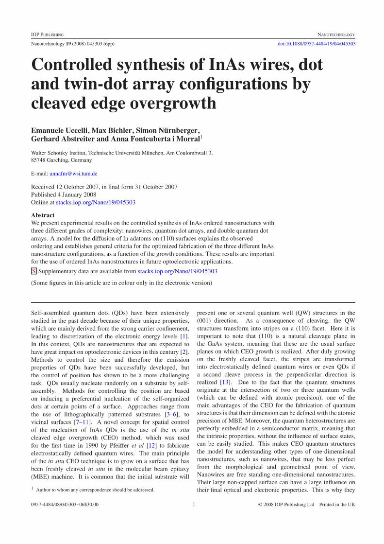
In the following we analyze the transition of the InAsconfigurations from wire to quantum dot arrays. For that,we investigate the onset of QD nucleation as a function ofthe InAs nominal thickness. In figure 2, AFM measurementson the same kind of surfaces with three different nominalInAs thicknesses are shown. For simplicity, only the set ofstripes containing the transition to QD formation are shown.From the top to the bottom of the figure, the measurementscorrespond to samples grown with respectively 3.2, 2.0 and 1.0nominal MLs of InAs. The color code indicates the relativeheight of the structures. Again, chains with heights from 10to 25 nm are observed, with identical periodicity to the AlAsstripes. Typically, Stranski–Krastanov type QDs present a
2
Nanotechnology 19 (2008) 045303 E Uccelli et al
Figure 2. Atomic force micrograph of a cleaved (110) surface,patterned by AlAs stripes of thickness from 12 to 21 nm aftergrowing three different InAs nominal thicknesses. The onset forquantum dot nucleation depends on the AlAs stripe thickness and theInAs nominal thickness.
lens-like shape, in which the height is much lower than thediameter [26, 27]. The formation of QDs with a nearly semi-spherical shape is striking, and may indicate the existence of aslightly different nucleation mechanism. As in figure 1, wiresand QD arrays are observed (QDs at the nucleation onset foreach sample are indicated with dashed circles). In agreementwith what has been presented above, the onset of QD formationoccurs on the thicker stripes. Moreover, we also observe thatthe onset of QD formation moves towards smaller AlAs stripewidths when the nominal InAs thickness is increased, whichcan be explained as follows. Let us assume that the criticalthickness of InAs for QD formation is tc. The amount of InAson the AlAs stripe (h) is proportional to the nominal InAsthickness (ML) and to the AlAs stripe width (d): h ∝ ML · d .This relation means that, for the nucleation of QD occurringat a given value of h = tc, if MLs are decreased, then d hasnecessarily to increase.
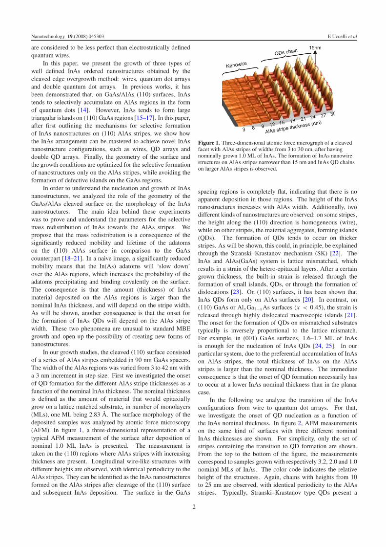
In this section, we quantify the results presented infigures 1 and 2, relate them to our growth model, providea more detailed understanding of the formation mechanismof the InAs nanostructures, and predict the formation of newstructures. The average dimension of the quantum dots (wire)was analyzed along each stripe as a function of the AlAs stripethickness, d , and the nominal InAs thickness. The results
Figure 3. Average height of the InAs nanostructure arrays as afunction of the thickness of the AlAs stripe, for three different InAsnominal thicknesses. A linear relation is found, with two mainregimes, having different slopes corresponding to the arrangement ofthe deposited InAs in the form of nanowire or quantum dot array.
are presented in figure 3. The relation between height of theQDs, h and d is linear and presents two different regimeswith different slopes. At small d values, h increases with aslope of 0.25 ± 0.05. After a certain onset there is a jump inthe value of h and the second slope depends on the amountof InAs deposited. The transition occurs exactly at the pointwhere the InAs nanostructures transform from wire to QDarray geometry. It is also important to note that the heightof the QDs in all cases is significantly larger than the nominalthickness deposited, indicating a strong migration of InAs fromthe neighboring areas, within the diffusion length distance(∼1 μm on (110) GaAs). In a first order approximation, thisallows us in the model to only consider one stripe and neglectthe effect of the neighboring stripes. In fact, the same topologyis observed for single stripe and multiple stripe geometries.The linear relation between h and d is a consequence ofthe lower mobility of In adatoms on (110) AlAs surfacesand, considering a very simplified one-dimensional model,follows [28]:
h ≈ d
τAlAs · DAlAs· LGaAs · M L = d ·
(LGaAs
L2AlAs
)· M L (1)
where ML is the number of nominal InAs monolayersdeposited, DAlAs and τAlAs are the effective diffusioncoefficient and lifetime of In adatoms on (110) AlAs stripes,and LAlAs and LGaAs are respectively the diffusion length of theIn adatom on AlAs and GaAs surfaces. Following equation (1)and in agreement with the experimental results, the heightincreases with the number of MLs. The slope of the curveh versus d depends on the In adatom diffusion length onboth GaAs and AlAs surfaces but in a different way. It isdirectly proportional to the indium diffusion length on theGaAs surface, while it is inversely proportional to the squareof the indium diffusion length on the AlAs surface. Due tothe deposition process, the value of the slope is a convolutionof the diffusion length on (110) oriented AlAs stripes and onthe growing InAs layers. The slope is slightly lower for thesamples grown with 1.0 ML. This could be due to the fact thatat 1 ML the diffusion length contains a higher contribution ofthe diffusion on bare AlAs, while at higher MLs the diffusionon InAs becomes predominant.
3
Nanotechnology 19 (2008) 045303 E Uccelli et al
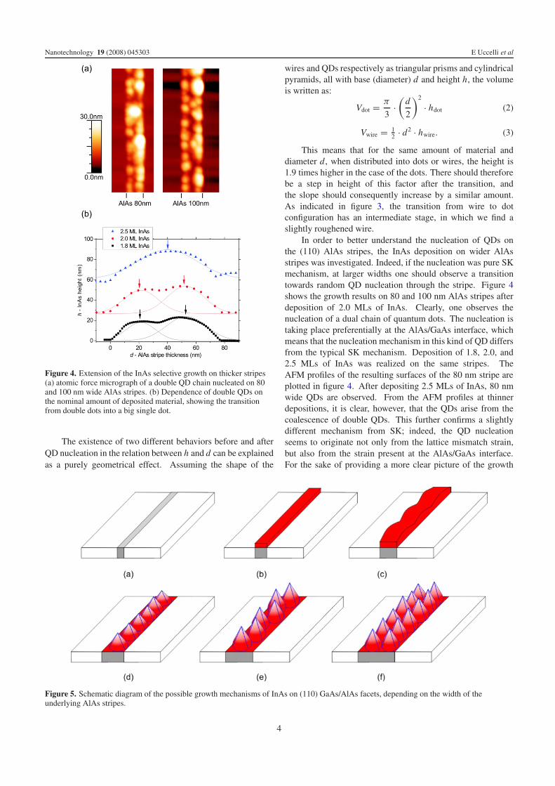
Figure 4. Extension of the InAs selective growth on thicker stripes(a) atomic force micrograph of a double QD chain nucleated on 80and 100 nm wide AlAs stripes. (b) Dependence of double QDs onthe nominal amount of deposited material, showing the transitionfrom double dots into a big single dot.
The existence of two different behaviors before and afterQD nucleation in the relation between h and d can be explainedas a purely geometrical effect. Assuming the shape of the
wires and QDs respectively as triangular prisms and cylindricalpyramids, all with base (diameter) d and height h, the volumeis written as:
Vdot = π
3·(
d
2
)2
· hdot (2)
Vwire = 12 · d2 · hwire. (3)
This means that for the same amount of material anddiameter d , when distributed into dots or wires, the height is1.9 times higher in the case of the dots. There should thereforebe a step in height of this factor after the transition, andthe slope should consequently increase by a similar amount.As indicated in figure 3, the transition from wire to dotconfiguration has an intermediate stage, in which we find aslightly roughened wire.
In order to better understand the nucleation of QDs onthe (110) AlAs stripes, the InAs deposition on wider AlAsstripes was investigated. Indeed, if the nucleation was pure SKmechanism, at larger widths one should observe a transitiontowards random QD nucleation through the stripe. Figure 4shows the growth results on 80 and 100 nm AlAs stripes afterdeposition of 2.0 MLs of InAs. Clearly, one observes thenucleation of a dual chain of quantum dots. The nucleation istaking place preferentially at the AlAs/GaAs interface, whichmeans that the nucleation mechanism in this kind of QD differsfrom the typical SK mechanism. Deposition of 1.8, 2.0, and2.5 MLs of InAs was realized on the same stripes. TheAFM profiles of the resulting surfaces of the 80 nm stripe areplotted in figure 4. After depositing 2.5 MLs of InAs, 80 nmwide QDs are observed. From the AFM profiles at thinnerdepositions, it is clear, however, that the QDs arise from thecoalescence of double QDs. This further confirms a slightlydifferent mechanism from SK; indeed, the QD nucleationseems to originate not only from the lattice mismatch strain,but also from the strain present at the AlAs/GaAs interface.For the sake of providing a more clear picture of the growth
Figure 5. Schematic diagram of the possible growth mechanisms of InAs on (110) GaAs/AlAs facets, depending on the width of theunderlying AlAs stripes.
4
Nanotechnology 19 (2008) 045303 E Uccelli et al
Figure 6. Atomic force micrographs showing the occurrence of InAs triangular defect density on (110) GaAs surfaces, as a function of theInAs nominal thickness. The nucleation of defects is avoided only at a nominal thickness of 1.0 ML.
mechanism for InAs nanostructures on (110) AlAs stripes, aschematic diagram for the selective InAs deposition model asa function of the nominal thickness is presented in figure 5.
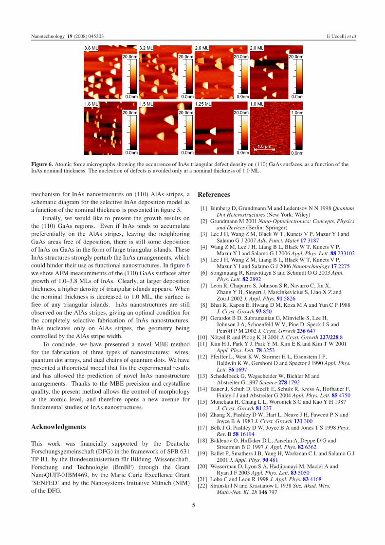
Finally, we would like to present the growth results onthe (110) GaAs regions. Even if InAs tends to accumulatepreferentially on the AlAs stripes, leaving the neighboringGaAs areas free of deposition, there is still some depositionof InAs on GaAs in the form of large triangular islands. TheseInAs structures strongly perturb the InAs arrangements, whichcould hinder their use as functional nanostructures. In figure 6we show AFM measurements of the (110) GaAs surfaces aftergrowth of 1.0–3.8 MLs of InAs. Clearly, at larger depositionthickness, a higher density of triangular islands appears. Whenthe nominal thickness is decreased to 1.0 ML, the surface isfree of any triangular islands. InAs nanostructures are stillobserved on the AlAs stripes, giving an optimal condition forthe completely selective fabrication of InAs nanostructures.InAs nucleates only on AlAs stripes, the geometry beingcontrolled by the AlAs stripe width.
To conclude, we have presented a novel MBE methodfor the fabrication of three types of nanostructures: wires,quantum dot arrays, and dual chains of quantum dots. We havepresented a theoretical model that fits the experimental resultsand has allowed the prediction of novel InAs nanostructurearrangements. Thanks to the MBE precision and crystallinequality, the present method allows the control of morphologyat the atomic level, and therefore opens a new avenue forfundamental studies of InAs nanostructures.
Acknowledgments
This work was financially supported by the DeutscheForschungsgemeinschaft (DFG) in the framework of SFB 631TP B1, by the Bundesministerium fur Bildung, Wissenschaft,Forschung und Technologie (BmBF) through the GrantNanoQUIT-01BM469, by the Marie Curie Excellence Grant‘SENFED’ and by the Nanosystems Initiative Munich (NIM)of the DFG.
References
[1] Bimberg D, Grundmann M and Ledentsov N N 1998 QuantumDot Heterostructures (New York: Wiley)
[2] Grundmann M 2001 Nano-Optoelectronics: Concepts, Physicsand Devices (Berlin: Springer)
[3] Lee J H, Wang Z M, Black W T, Kunets V P, Mazur Y I andSalamo G J 2007 Adv. Funct. Mater 17 3187
[4] Wang Z M, Lee J H, Liang B L, Black W T, Kunets V P,Mazur Y I and Salamo G J 2006 Appl. Phys. Lett. 88 233102
[5] Lee J H, Wang Z M, Liang B L, Black W T, Kunets V P,Mazur Y I and Salamo G J 2006 Nanotechnology 17 2275
[6] Songmuang R, Kiravittaya S and Schmidt O G 2003 Appl.Phys. Lett. 82 2892
[7] Leon R, Chaparro S, Johnson S R, Navarro C, Jin X,Zhang Y H, Siegert J, Marcinkevicius S, Liao X Z andZou J 2002 J. Appl. Phys. 91 5826
[8] Bhat R, Kapon E, Hwang D M, Koza M A and Yun C P 1988J. Cryst. Growth 93 850
[9] Gerardot B D, Subramanian G, Minvielle S, Lee H,Johnson J A, Schoenfeld W V, Pine D, Speck J S andPetroff P M 2002 J. Cryst. Growth 236 647
[10] Notzel R and Ploog K H 2001 J. Cryst. Growth 227/228 8[11] Kim H J, Park Y J, Park Y M, Kim E K and Kim T W 2001
Appl. Phys. Lett. 78 3253[12] Pfeiffer L, West K W, Stormer H L, Eisenstein J P,
Baldwin K W, Gershoni D and Spector J 1990 Appl. Phys.Lett. 56 1697
[13] Schedelbeck G, Wegscheider W, Bichler M andAbstreiter G 1997 Science 278 1792
[14] Bauer J, Schuh D, Uccelli E, Schulz R, Kress A, Hofbauer F,Finley J J and Abstreiter G 2004 Appl. Phys. Lett. 85 4750
[15] Munekata H, Chang L L, Woronick S C and Kao Y H 1987J. Cryst. Growth 81 237
[16] Zhang X, Pashley D W, Hart L, Neave J H, Fawcett P N andJoyce B A 1983 J. Cryst. Growth 131 300
[17] Belk J G, Pashley D W, Joyce B A and Jones T S 1998 Phys.Rev. B 58 16194
[18] Baklenov O, Huffaker D L, Anselm A, Deppe D G andStreetman B G 1997 J. Appl. Phys. 82 6362
[19] Ballet P, Smathers J B, Yang H, Workman C L and Salamo G J2001 J. Appl. Phys. 90 481
[20] Wasserman D, Lyon S A, Hadjipanayi M, Maciel A andRyan J F 2003 Appl. Phys. Lett. 83 5050
[21] Lobo C and Leon R 1998 J. Appl. Phys. 83 4168[22] Stranski I N and Krastanow L 1938 Sitz. Akad. Wiss.
Math.-Nat. Kl. 2b 146 797
5

Nanotechnology 19 (2008) 045303 E Uccelli et al
[23] Shchukin V A, Ledentsov N N and Bimberg D 2004 Epitaxy ofNanostructures (Berlin: Springer)
[24] Goldstein L, Glas F, Marzin J Y, Charasse M N andLe Roux G 1985 Appl. Phys. Lett. 47 1099
[25] Kobayashi N P, Ramachandran T R, Chen P andMadhukar A 1996 Appl. Phys. Lett. 68 3299
[26] Moison J m, Houzay F, Barthe F, Leprince L, Andre E andVatel O 1994 Appl. Phys. Lett 64 196
[27] Lee J H, Wang Z M, Liang B L, Sablon K A, Strom N W andSalamo G J 2006 Semicond. Sci. Technol. 21 1547
[28] Uccelli E et al 2007 Superlattices Microstruct. submitted
6
Related Documents


![Structure of protease-cleaved Escherichia coli [alpha]-2 ...](https://static.cupdf.com/doc/110x72/6254e603fdeb8a7b8416fee8/structure-of-protease-cleaved-escherichia-coli-alpha-2-.jpg)