University of Connecticut OpenCommons@UConn Doctoral Dissertations University of Connecticut Graduate School 4-7-2015 Control Strategies of Power Electronic Converters to Improve the Reliability and Stability of Renewable Energy Systems Tai-Sik Hwang University of Connecticut - Storrs, [email protected] Follow this and additional works at: hps://opencommons.uconn.edu/dissertations Recommended Citation Hwang, Tai-Sik, "Control Strategies of Power Electronic Converters to Improve the Reliability and Stability of Renewable Energy Systems" (2015). Doctoral Dissertations. 699. hps://opencommons.uconn.edu/dissertations/699

Welcome message from author
This document is posted to help you gain knowledge. Please leave a comment to let me know what you think about it! Share it to your friends and learn new things together.
Transcript

University of ConnecticutOpenCommons@UConn
Doctoral Dissertations University of Connecticut Graduate School
4-7-2015
Control Strategies of Power Electronic Convertersto Improve the Reliability and Stability ofRenewable Energy SystemsTai-Sik HwangUniversity of Connecticut - Storrs, [email protected]
Follow this and additional works at: https://opencommons.uconn.edu/dissertations
Recommended CitationHwang, Tai-Sik, "Control Strategies of Power Electronic Converters to Improve the Reliability and Stability of Renewable EnergySystems" (2015). Doctoral Dissertations. 699.https://opencommons.uconn.edu/dissertations/699

Control Strategies of Power Electronic Converters to Improve the Reliability
and Stability of Renewable Energy Systems
Tai-Sik Hwang, Ph.D
University of Connecticut, 2015
This dissertation discusses control strategies for power electronic converters that improve the
reliability and stability of renewable energy systems. Three approaches are proposed to improve the
control performance of a dc-dc converter and a distributed generation (DG) inverter under different
operation modes and fault conditions.
First, a seamless control for the dc-dc converter with both discontinuous conduction mode (DCM)
and continuous conduction mode (CCM) is proposed. The plant models in DCM and CCM are different
in the frequency domain. Therefore, it is difficult to design a controller with stable operation and fast
response in both modes. The proposed controller can make mode transitions between DCM and CCM
seamlessly with a mode tracker, and then the boost converter can autonomously operate by selecting the
appropriate control loop in both modes.
Second, a seamless control for the DG inverter with both a grid connected (GC) mode and a
standalone (SA) mode is presented. With increasing renewable DGs, fast and stable mode transition
technologies are necessary not only for sending the power to the grid in the GC mode, but also for
protecting DGs from grid fault conditions in the SA mode. The proposed controller consists of a current
controller and a feedforward voltage controller to minimize the grid overvoltage and improve the voltage
response.

Tai-Sik Hwang – University of Connecticut, 2015
Third, a control strategy to suppress a dc power oscillation of the DG inverter under grid voltage
unbalance is discussed. Due to voltage unbalance, the dc power oscillation is generated, which impacts
the lifespan of the renewable energy sources. A modified synchronous reference frame based current
control with improved current reference is proposed. With the proposed current loop, the dc power
oscillation is reduced effectively.
The proposed control strategies reduce the impact of the renewable energy and the load under faults or
disturbance conditions. And the stable operation of the power electronic converters will also enhance the
stability and reliability of the renewable energy, the grid, and the load.

Control Strategies of Power Electronic Converters to Improve the Reliability and
Stability of Renewable Energy Systems
Tai-Sik Hwang
B.S., Yeungnam University, 2004
M.S., Yeungnam University, 2006
A Dissertation
Submitted in Partial Fulfillment of the
Requirements for the Degree of Doctor of Philosophy
at the University of Connecticut
2015

i
Copyright by
Tai-Sik Hwang
2015

ii
APPROVAL PAGE
Doctor of Philosophy Dissertation
Control Strategies of Power Electronic Converters to Improve the Reliability and Stability
of Renewable Energy Systems
Presented by
Tai-Sik Hwang, B.S., M.S.
Major Advisor ___________________________________________________________________
Sung-Yeul Park
Associate Advisor ___________________________________________________________________
Krishna R. Pattipati
Associate Advisor ___________________________________________________________________
Ali M. Bazzi
Associate Advisor ___________________________________________________________________
Shalabh Gupta
University of Connecticut
2015

iii
ACKNOWLEDGMENTS
I would never have been able to finish my dissertation without the guidance of my committee
members. I would like to thank my advisor, Prof. Sung-Yeul Park for his patience, and supporting for my
research. I would like to thank Prof. Krishna R. Pattipati, who helps and supports my job applications. I
would like to thank my committee members, Prof. Ali M. Bazzi and Prof. Shalabh Gupta for their
encouragement, insightful comments, and hard questions.
I would like to thank Sungmin Park, Ph.d and Yongduk Lee, Ph.d Candidate, who as my good lab
members were always willing to help and give their best suggestions. I thank to Matthew Tarca and other
members in the laboratory. My research would not have been possible without their helps.
I would also like to thank my mother, and two sisters. They were always supporting me and
encouraging me with their best wishes.

iv
TABLE OF CONTENTS
CHAPTER 1. INTRODUCTION ................................................................................................................. 1
1.1 Overview ............................................................................................................................................. 1
1.2 Problem Statement .............................................................................................................................. 2
1.2.1 Control of dc-dc converter with mode transition ......................................................................... 2
1.2.2 Control of DG inverter with mode transition ............................................................................... 3
1.2.3 Control of DG inverter under grid distortion ................................................................................... 4
1.3 Dissertation Organization ................................................................................................................... 5
CHAPTER 2. LITERATURE REVIEW ..................................................................................................... 6
2.1 Control of dc-dc converter with mode transition ................................................................................ 6
2.2.1 Dc-dc converter for fuel cell applications .................................................................................... 6
2.1.2 Control of dc-dc converter with mode transition ......................................................................... 8
2.2 Control of DG Inverter with mode transition .................................................................................... 10
2.2.1 Current control in the GC mode ................................................................................................. 10
2.2.2 Voltage control in the SA mode ................................................................................................. 11
2.2.3 Mode transition approach ........................................................................................................... 11
2.3 Control of DG inverter under grid voltage unbalance ...................................................................... 14
CHAPTER 3. SEAMLESS CONTROL OF DC-DC CONVERTERS BETWEEN DCM AND CCM ..... 17
3.1 Boost Converter Modeling In DCM and CCM ................................................................................. 17
3.1.1 Small signal modeling in CCM and DCM ................................................................................. 17
3.1.2 Mode Boundary [113] ................................................................................................................ 19
3.1.3 Issues with Designing the Controller for both CCM and DCM ................................................. 20
3.2 Proposed Controller Design in DCM and CCM ............................................................................... 22
3.2.1 Current Control in CCM [114] ................................................................................................... 22
3.2. 2 Feedforward Current Control in DCM ...................................................................................... 23
3.2. 3 Voltage Control in both CCM and DCM .................................................................................. 24
3.2. 4 Proposed Seamless Control System with Mode Tracker .......................................................... 26
3.2.5 Stability and Robustness of Seamless Mode Transition ............................................................ 27
3.2.6 Transient Response during the mode transition ......................................................................... 31
3.3 Simulation Results ............................................................................................................................ 31
3.4 Experimental Results ........................................................................................................................ 34
3.5 Conclusion ........................................................................................................................................ 37

v
CHAPTER 4. SEAMLESS CONTROL OF DG INVETERS FOR MODE TRANSITIONS UNDER
GRID DISTURBANCE .............................................................................................................................. 39
4.1 Impact of DG Inverter in Overvoltage Conditions ........................................................................... 39
4.1.1 Mode transitions of DG inverter in Overvoltage Conditions ..................................................... 39
4.1.2 Mode transition in the overvoltage due to PCC switch-off ........................................................ 40
4.1.3 Mode transition in the overvoltage due to grid voltage swell .................................................... 41
4.1. 4 Requirements for Fast Mode transition of DG inverter in overvoltage conditions ................... 42
4.2 Conventional DG Inverter Control with Operational Modes ............................................................ 43
4.2.1 DG inverter Modeling in GC mode and SA mode (Appendix A) ............................................. 43
4.2.2 Current Control in GC mode ...................................................................................................... 46
4.2.3 Voltage control in SA mode ....................................................................................................... 48
4.2.4 Performance and Limitation of Voltage Control in the overvoltage conditions ........................ 48
4.3 Seamless Control Strategy in Overvoltage Conditions ..................................................................... 52
4.3.1 Proposed controller configuration .............................................................................................. 52
4.3.2 Current Reference Calculation with respect to Operational Modes ........................................... 53
4.3.3 Current Control with Feed forward Voltage loop ...................................................................... 54
4.4 Simulation Results ............................................................................................................................ 57
4.5 Experimental Results ........................................................................................................................ 62
4.5.1 Hardware- In- the Loop Test using RTDS ................................................................................. 62
4.5.2 Experimental Wave forms ......................................................................................................... 63
4.6 Conclusion ........................................................................................................................................ 66
CHAPTER 5. CONTROL OF LCL FILTER BASED DG INVERTERS TO SUPPRESS DC POWER
OSCILLATION UNDER GRID VOLTAGE UNBALANCE ................................................................... 67
5.1 Control overview of LCL filter based DG inverter under grid voltage unbalance ........................... 67
5.2 Impact of DG Inverter under Grid Voltage Unbalance ..................................................................... 69
5.1.1 DG inverter modeling under unbalanced grid voltage ............................................................... 69
5.1.2 Dc power oscillation due to oscillating ac power under grid voltage unbalance ....................... 71
5.2 Performance of Conventional Control Scheme................................................................................. 74
5.2.1 Conventional current reference calculations [98] ...................................................................... 74
5.2.3 Conventional double synchronous reference frame current control [98] ................................... 76
5.3 Proposed Control Scheme for Suppression of DC Power Oscillation .............................................. 80
5.3.1 Improved current reference calculation ..................................................................................... 80
5.3.2 State Vector under Unbalance Operating Conditions ................................................................ 81
5.3.2 Modified transformation on the unbalanced rotation frame ....................................................... 85

vi
5.3.3 Dynamic voltage equation on the unbalanced rotating frame .................................................... 87
5.3.4 Unbalanced grid voltage compensation on the unbalanced rotating frame................................ 90
5.3.5 Proposed control scheme ........................................................................................................... 92
5.4 Simulation Results ............................................................................................................................ 93
5.5 Experimental Results ........................................................................................................................ 95
5.6 Conclusion ........................................................................................................................................ 97
CHAPTER 6. SUMMARY AND FUTURE WORKS ............................................................................... 98
APPENDIX A. MODELING OF THEREE PHASE LCL FILTER BASED DC-AC INVERTER ......... 101
A.1 Dc-ac inverter modeling in the abc axis ........................................................................................ 101
A.2 α-β / d-q dc-ac inverter modeling using a vector notation ................................................................. 101
A.3 α-β / d-q dc-ac inverter modeling using a complex space vector notation ..................................... 103
APPENDIX B. GENERAL COMPLEX SPACE VECTOR .................................................................... 106
APPENDIX C. SYMMETRICAL COORDINATE ANALYSIS ............................................................ 107
APPENDIX D. ROTATION OF AXES ................................................................................................... 109
REFERENCES ......................................................................................................................................... 111

vii
LIST OF TABLES
TABLE I. Ratings and Known Parameters of Boost Converter and Control System.................................32
TABLE II. Parameters with respect to power consumption of the critical load..........................................46
TABLE III. Comparison of Controllers Performance for Mode Transition................................................61

viii
LIST OF FIGURES
Fig. 1. The role of the power electronic converters in renewable energy systems........................................1
Fig. 2. Control scheme of the dc-dc converter...............................................................................................3
Fig. 3. Control scheme of the DG inverter with respect to operational modes.............................................4
Fig. 4. Control scheme of the DG inverter under grid voltage unbalance and harmonics. ...........................4
Fig. 5. V-I characteristics of the DBFC.........................................................................................................6
Fig. 6. Block diagram of adaptive tuning algorithm for dc-dc converter......................................................8
Fig. 7. Mixed-mode operation of boost switch-mode rectifier......................................................................9
Fig. 8. MCFC power plant...........................................................................................................................12
Fig. 9. DG inverter system configuration with mode transition..................................................................13
Fig. 10. Indirect current control for seamless transfer of three-phase utility interactive inverters..............14
Fig. 11. Dual current control scheme in synchronous reference frame for PWM converter under
unbalanced input voltage conditions............................................................................................................15
Fig. 12. New stationary frame control scheme for three-phase PWM rectifiers under unbalanced voltage
dips conditions.............................................................................................................................................15
Fig. 13. Boost converter configuration........................................................................................................18
Fig. 14. Frequency responses of the duty ratio-to-output voltage transfer function in CCM and DCM.....21
Fig. 15. Loop gains of compensator according to DCM and CCM.............................................................21
Fig. 16. Block diagram of proposed current control with nonlinear feedforward in CCM.........................23
Fig. 17. Block diagram of feedforward current control in DCM.................................................................23
Fig. 18. Block diagram of voltage control in CCM.....................................................................................24
Fig. 19. Block diagram of voltage control in DCM.....................................................................................25
Fig. 20. Proposed control block diagram with a mode tracker....................................................................27
Fig. 21. Mixed control block diagram with respect to the operation mode and mk .....................................28
Fig. 22. Bode plot of ( )1T s ( 0.4 0.6mk≤ ≤ )....................................................................................................30

ix
Fig. 23. Bode plot of ( )2T s ( 0.4 0.6mk≤ ≤ )....................................................................................................30
Fig. 24. Simplified control block diagram...................................................................................................31
Fig. 25. Simulation waveform of transient response (10Ω → 25 Ω→ 10 Ω)..............................................33
Fig. 26. Simulation waveform of transient response (10Ω → 100 Ω→ 10 Ω) ...........................................33
Fig. 27. Simulation waveform of transient response (50Ω → 25 Ω → 16.7 Ω → 12.5 Ω) ........................33
Fig. 28. DBFC and boost converter system.................................................................................................34
Fig. 29. Test waveform of transient response in proposed mixed controller (Input voltage: 6.0V, Load : 25
Ω ↔ 10 Ω)...................................................................................................................................................35
Fig. 30. Test waveform of transient response (Input voltage: 4.5V, Load: 40 Ω 10 Ω).........................36
Fig. 31. Test waveform of transient response (Input voltage: 4.5V, Load: 10 Ω 120 Ω).......................37
Fig. 32. Occurrence of the critical load faults during conventional mode transition in the overvoltage.....40
Fig. 33. Overvoltage due to PCC switch-off................................................................................................41
Fig. 34. Overvoltage due to main grid voltage............................................................................................42
Fig. 35. Control state during fast mode transition........................................................................................43
Fig. 36. Circuit diagram of the DG inverter with the grid and the critical load...........................................44
Fig. 37. Transfer function block diagram of the DG inverter......................................................................46
Fig. 38. Transfer function block diagram of DG inverter in GC mode.......................................................47
Fig. 39. Transfer function block diagram of DG inverter in SA mode........................................................47
Fig. 40. Current control block diagram in GC mode...................................................................................48
Fig. 41. Voltage control block diagram in SA mode...................................................................................48
Fig. 42. Simplified voltage control loop with current loop in SA mode......................................................49
Fig. 43. Responses of the voltage control with current loop according to the critical load type.................50
Fig. 44. Simplified voltage control loop without the current control loop in SA mode..............................51
Fig. 45. Responses of the voltage control without current loop according to the critical load type............52
Fig. 46. Proposed overall control block diagram.........................................................................................52
Fig. 47. State flow diagram for operational mode decision in overvoltage conditions...............................54

x
Fig. 48. Block diagram of the simplified current control with feed forward voltage loop in SA mode......55
Fig. 49. Responses of the current control with feedforward voltage loop according to the critical load
type...............................................................................................................................................................56
Fig. 50. Simulation results of the conventional mode transition from the current control to the voltage
control with the current loop. PCC switch-off period with..........................................................................57
Fig. 51. Simulation results of the conventional mode transition from the current control to the voltage
control without the current loop...................................................................................................................59
Fig. 52. Simulation results of the proposed mode transition in current control with feedforward voltage
loop...............................................................................................................................................................60
Fig. 53. Experimental setup of hardware in the loop using RTDS..............................................................62
Fig. 54. Experimental waveform of current control in GC mode during PCC switch-off period with
3.3kW resistive load.....................................................................................................................................63
Fig. 55. Experimental waveforms of conventional mode transition using the voltage control without
current loop..................................................................................................................................................64
Fig. 56. Experimental waveforms of the proposed mode transition using the current control with
feedforward voltage loop.............................................................................................................................65
Fig. 57. Experimental waveforms of the proposed mode transition using the current control with
feedforward voltage loop.............................................................................................................................65
Fig. 58. Control overview to suppress dc power oscillation under grid voltage unbalance........................68
Fig. 59. Power flow of the LCL filter based DG inverter under unbalanced grid voltage..........................69
Fig. 60. Block diagram of the dc power ripple generation under unbalanced grid voltage.........................73
Fig. 61. Simulation waveforms of dc voltage and current oscillation suppression using conventional
current reference..........................................................................................................................................75
Fig. 62. Block diagram of conventional double d-q frame current control.................................................76
Fig. 63. Simplified double d-q frame current control loop..........................................................................79

xi
Fig. 64. Step responses of conventional d-q frame current controllers of L and LC filters based
inverter.........................................................................................................................................................79
Fig. 65. Positive- and negative-sequence synchronous reference frames....................................................82
Fig. 66. Loci of positive- and negative-sequence sate vectors and unbalanced sate vector in the α-β
axis...............................................................................................................................................................83
Fig. 67. Rotation of axes between general ellipse and standard ellipse.......................................................84
Fig. 68. Scaling between canonical ellipse and circle..................................................................................84
Fig. 69. Comparison between the δ-γ transformation and the d-q transformation under unbalanced
operating conditions...................................................................................................................................87
Fig. 70. Loci of unbalanced current and voltage vectors in the α-β axis.....................................................90
Fig. 71. Block diagram of current control loop in the δ-γ axis....................................................................90
Fig. 72. Bode plot of LCL filter with active damping................................................................................91
Fig. 73. Proposed control block diagram for dc power oscillation suppression..........................................92
Fig. 74. Simulation waveforms of d-q axis output current, dc voltage, and dc current with conventional
and proposed control schemes.....................................................................................................................93
Fig. 75. Simulation waveforms of the α-β axis current and the δ-γ axis current of proposed control
scheme..........................................................................................................................................................94
Fig. 76. Simulation waveforms of three phase voltage, current, and dc power of proposed control
scheme..........................................................................................................................................................94
Fig. 77. Experimental setup of hardware in the loop using RTDS and dSPACE........................................95
Fig. 78. Experimental waveforms of conventional current control under balanced grid voltage................96
Fig. 79. Experimental waveforms of conventional current control under unbalanced grid voltage............96
Fig. 80. Experimental waveforms of proposed current control under unbalanced grid voltage.................96
Fig. 81 Circuit diagram of three phase LCL filter based dc-ac inverter....................................................101
Fig. 82. Loci of space vectors in the α-β axis and their waveforms in time domain................................106
Fig. 83. Rotation of axes............................................................................................................................109

1
CHAPTER 1. INTRODUCTION
1.1 Overview
The importance of power electronic converters such as dc-dc converters and voltage source inverters
is increasing due to increasing distribution-level penetration of renewable energy sources such as
photovoltaic and fuel cell technologies. Fig. 1 shows the role of power electronic converters in renewable
energy systems. Power electronic converters should send power by regulating dc - dc or dc - ac to the
electrical load and the utility grid. Since they are interfaced with renewable sources and electrical loads or
the grid, the performance of power electronic converters depends on interactions among sources, loads,
and their state of operation. Power electronic converters should be operated with safety and stability under
normal conditions, fault conditions, overloads, and different operation modes. However performance of
conventional controllers of power electronics converters is limited to minimize impacts on disturbances
due to fault conditions and to control different operation modes seamlessly. Therefore, enhanced control
strategies of power electronic converters are important to improve the reliability of renewable energy
sources and the stability of the grid and the load.
Fig. 1. The role of the power electronic converters in renewable energy systems

2
This dissertation discusses enhanced control strategies for power electronic converters that improve
the reliability and stability of renewable energy systems. First, seamless control for the dc-dc converter
with both discontinuous conduction mode (DCM) and continuous conduction mode (CCM) is discussed.
Second, a seamless control strategy for the distributed generation (DG) inverter with both a grid
connected (GC) mode and a standalone (SA) mode is presented. Third, control strategies for suppression
of a dc power oscillation and an ac current distortion of the DG inverter under grid voltage unbalance is
discussed. The proposed control strategies reduce the impact of the renewable energy and the load under
faults or disturbance conditions. And the stable operation of the power electronic converters will also
enhance the stability and reliability of the renewable energy, the grid, and the load.
1.2 Problem Statement
Three control problems are discussed to improve the control performance of the dc-dc converter and
the DG inverter under different operation modes and fault conditions; 1) a control of the dc-dc converter
with both DCM and CCM, 2) a control of the DG inverter with both the GC mode and the SA mode, and
3) a control to suppress a dc power oscillation of the DG inverter under grid voltage unbalance.
1.2.1 Control of dc-dc converter with mode transition
Fig. 2 shows a typical control scheme of the dc-dc converter. The dc-dc converter operates either in
DCM or in CCM. The operation mode is determined by the duty ratio, load and parameters of the dc-dc
converter. In particular, it is well known that different mode of the boost converter operation can result in
very different dynamics between CCM and DCM plants. Therefore, it will be difficult to design a
controller with stable operation and fast transient response for both modes. Moreover, if the dc-dc
converter operates in CCM with the DCM control gain or vice versa, it will be unstable.
The CCM boost converter has limitation, which is the resonance point due to double poles and non-
minimum phase due to a right half plane zero (RHPZ). Therefore, the CCM boost converter is difficult to
design with a compensator of wide range operation. This problem has been solved by designing a
conventional voltage-mode control at a low control bandwidth. However, the conventional voltage-mode

3
control is difficult to obtain fast response time of voltage regulation in both modes because of different
dynamics. Therefore the boost converter for portable fuel cell applications is required to operate from
very light load (DCM) to regular load (CCM) conditions with a fast and smooth response.
Fig. 2. Control scheme of the dc-dc converter
1.2.2 Control of DG inverter with mode transition
Fig. 3 shows a control scheme of the DG inverter with respect to operational modes. The response time
of the voltage controller depends on the critical load variation. The fast mode transition can make
unexpected control mode in the overvoltage condition due to the grid voltage swell. The voltage control
of the DG inverter connected to the grid is not able to regulate the grid voltage. It will cause the voltage
control instability in the worst case. Even though the DG inverter still operates with the voltage control
loop for grid connection within short duration, it needs to be changed from the voltage control to the
current control in the overvoltage condition due to the grid voltage swell. The voltage control is required
to have a fast response time under critical load variation to order to make the fast mode transition in the
overvoltage condition due to point common coupling (PCC) switch-off. Therefore, the voltage control is
necessary to be designed with considering plants in GC and SA modes. It will satisfy a seamless control
of the DG inverter with the critical load safety in overvoltage conditions.

4
Fig. 3. Control scheme of the DG inverter with respect to operational modes.
1.2.3 Control of DG inverter under grid distortion
Fig. 4 shows a control scheme of the DG inverter under grid voltage unbalance. Conventionally, the
double synchronous reference frame current controller is designed with the current reference calculation
to suppress the dc voltage oscillation in the L filter based DG inverter. The LCL filter based DG inverter
is limited to minimize both dc current and dc voltage oscillations by the conventional reference
calculation. Additional current through the capacitor is generated in the LCL filter. However, the
conventional current reference calculation is derived with considering the L filter based DG inverter,
which assumes that the inverter current is equal to the output current. Therefore, the conventional current
calculation is not able to suppress dc voltage and dc current oscillations in the LCL filter based DG
inverter.
Fig. 4. Control scheme of the DG inverter under grid voltage unbalance and harmonics

5
1.3 Dissertation Organization
This dissertation is composed of six chapters. The first chapter introduces the importance of control
of the power electronic converters in renewable systems and the issues on existing power electronic
converter systems. The literature review of control strategies for power electronic converters is presented
in chapter 2. Chapter 3 explains a seamless control scheme for the dc-dc converter with different
operation modes for both DCM and CCM. Chapter 4 discusses a seamless control for the DG inverter
under grid disturbances. Chapter 5 presents a control of LCL filter based DG inverters to suppress the dc
power oscillation under unbalanced operating conditions is discussed. In chapter 6, this dissertation is
summarized with future works.

6
CHAPTER 2. LITERATURE REVIEW
2.1 Control of dc-dc converter with mode transition
2.2.1 Dc-dc converter for fuel cell applications
The direct borohydride fuel cell (DBFC) is directly fed sodium borohydride as a fuel and hydrogen
peroxide as the oxidant. It can be used as the power source for portable applications. Fig. 5 shows the V-I
characteristics of the DBFC. It can be seen that if the initial non-linearity (activation polarization) and
high current region (concentration polarization) are neglected, the DBFC works in a nearly linear region
(ohmic polarization). Considering the linear region, the output voltage of the DBFC varies according to
the output current, because of its typical V-I characteristic [1]. Therefore, a dc-dc converter is necessary
to regulate the output voltage. In addition, ripple current reduction of the fuel cell is important to increase
the life time of a fuel cell stack [2], [3].
Fig. 5. V-I characteristics of the DBFC [19].
Most fuel cell power converters are expected to produce power on demand, also known as load
following power sources. However, the response time of the fuel cells are typically known to be slower
than those of other power sources such as batteries and diesel engines. This is because of the operation of
the balance of plant (BOP) associated with mass and heat balances inside and outside the stack. In order

7
to improve the response time, many fuel cell systems are combined with a battery or capacitor to form a
hybrid power generation system [4], [5].
A bidirectional dc–dc converter, which is used to interface an ultracapacitor as energy storage to a fuel
cell, was presented in [6] and [7]. These papers have shown that the bidirectional converter with the
ultracapacitor had better control response times for a fuel cell system during voltage transients.
References [8] and [9] proposed a novel hybrid fuel cell power conditioning system. This system consists
of the fuel cell, a battery, a unidirectional dc–dc converter, a bidirectional dc–dc converter, and a dc-ac
inverter. A fuel cell and a battery are connected to the common dc bus for the unidirectional dc–dc
converter and the bidirectional dc–dc converter.
References [10] and [11] reviewed some of the characteristics of fuel cell applications. A discussion of
important considerations for fuel cell converter design is presented. The role of the fuel cell controller
was briefly introduced. Reference [12] focused on the design of a dc–dc converter, control, and auxiliary
energy storage system. A novel converter configuration, which improves utilization of the high frequency
transformer and simplifies the overall system control, was proposed.
Stability analysis of fuel cell powered dc-dc converters was also discussed in [13]. An equivalent
circuit model based on the chemical reactions inside of the fuel cell was presented. It showed that fuel cell
internal impedance can significantly affect the dynamics of the dc-dc converter. Also, the behavior of the
fuel cell during purging has been discussed. In order to overcome these problems, the supercapacitor
connected in parallel with the fuel cell was proposed. An impedance analysis approach had been proposed
in [14] and [15]. It showed the static response of the overall system with the fuel cell and the dc-dc
converter. However, it did not clearly show the impact of the individual components.
In [16] and [17], the input impedance of the boost power factor correction converter for both the
conventional current controller and the duty ratio feedforward controller were explained theoretically.
Due to the nonlinearity and unstable zero dynamics of the boost converter, it has some limitations such as
low bandwidth and poor dynamic response [18], [19]. In order to solve this drawback, a novel nonlinear
control strategy based on input-output feedback linearization was proposed in [20] and [21].

8
2.1.2 Control of dc-dc converter with mode transition
The dc-dc converter can be operated in either continuous conduction mode (CCM) or discontinuous
conduction mode (DCM). In particular, it is well known that different the boost converter operation
modes can result in very different dynamics in the frequency domain. This problem can be solved by
designing a conventional voltage-mode control at a low control bandwidth. This can make a stable
operation at the critical boundary condition during the transition of the operation mode [22].
In the past two decades, many studies have been done to model dc-dc converters in DCM and CCM.
An averaged modelling of dc-dc converters operating in DCM was studied in [23] and [24]. In DCM,
these models are represented either as analytical equations or equivalent circuits, and fall into both
reduced-order models and full-order models [23]. A method which includes generation, classification and
analysis of dc-dc converters was presented in [25]. Three DCM modes of dc-dc converters considered in
[26] are the discontinuous inductor current mode, the discontinuous capacitor voltage mode, and an
unidentified mode called the discontinuous quasi-resonant mode. A circuit based approach to the analysis
of dc-dc converters was presented in [27]. This method was focused on the identification of a three-
terminal nonlinear device in the dc-dc converter. An exact small-signal discrete-time model for digitally
controlled dc-dc converters operating in CCM was presents in [28]. The analysis of open-loop dynamics
relevant to current-mode control for a boost converter operating in CCM was presents in [29]. An
averaged state-space modelling of dc-dc converters in CCM and DCM have been developed in [30].
Fig. 6. Block diagram of adaptive tuning algorithm for dc-dc converter [22]

9
On the other hand, an adaptive tuning algorithm of digital voltage-mode controllers for dc-dc converter
was presented to transfer from DCM to CCM [22]. This approach is able to maintain a high performance
control without the stability issues by using additional hardware configuration to detect the operation
mode. A new hybrid control method was introduced from the basic circuit theory and implemented for the
output voltage regulation in the boost converter [31]. The proposed method was designed with analogue
and digital circuits. A mixed-mode predictive current control at constant but two different switching
frequencies for a single-phase boost power factor correction (PFC) converter has been proposed in [32].
The PFC converter showed the operation in either CCM or DCM depending on the load condition. A
simple digital DCM control algorithm in [33] was proposed in order to achieve minimal changes to the
average current control in CCM. The algorithm was mathematically and computationally simple. A
control scheme for sensorless operation and detection of both CCM and DCM in the dc-dc converter was
presented in [34]. The proposed controller utilized dual control loops and did not need the inductor
current feedback. A generalization of the recently proposed nonlinear average current control scheme for
DCM operation was described in [35]-[37]. The approach was to develop a nonlinear control method for
DCM operation by using the same control principle then combining the control method with that for
CCM operation.
Fig. 7. Mixed-mode operation of boost switch-mode rectifier [32]
A time domain control method of boost converters at the critical boundary condition is proposed to
achieve fast dynamic response time under load variations in [38]. Although it has the disadvantage of

10
requiring a sophisticated analogue circuit, the proposed method can provide fast transient response.
Interleaving methods for the critical boundary condition between DCM and CCM of boost PFC
converters with master and slave modes was thoroughly analyzed in [39]-[41]. With open and closed
loops, the slave converter can be synchronized to the turn-on or to the turn-off instant of the master
converter. In both modes, dc-dc converters can be operated by either current mode or voltage mode
controls. A dual mode control scheme was proposed in [42] to control a boost PFC converter. The
proposed method combined both CCM and the critical boundary condition and had the advantage of
simple control and high efficiency under light-load conditions.
However, none of the literature explained clearly how to minimize the impact of the mode transition
and implement fully digital control algorithms with a robust mode transition
2.2 Control of DG Inverter with mode transition
2.2.1 Current control in the GC mode
The use of the renewable energy is increasing rapidly at a growing rate. The growth in renewable
generation is expected to 26 percent of the total generation growth from 2009 to 2035 in U.S.A [43].
Therefore, utility companies have already begun to take into account not only the conventional
centralized power generation, transmission, and distribution, but also renewable energy based distributed
generations.
Most distributed generations (DG) is connected to the grid by using the voltage source dc-ac inverter.
The inverter controller stabilizes the dc-link voltage and supplies active and reactive powers to the grid by
regulating ac current at a certain power factor. The control schemes for the DG inverter are implemented
based on a synchronous reference frame control and a stationary reference frame control. The
synchronous reference frame current control or d-q current control regulates the d-q axis current with the
d-q transformation and proportional-integral (PI) controller. [44], [45], [46]. Stationary reference frame
control or the α-β current control regulates the α-β axis current from the α-β transformation and
proportional-resonant (PR) controller [47]–[51]. As a kind of fast current controller, it is known that dead-

11
beat or predictive controllers provide the fastest response time. However, there could be the stability issue
because of the delay time and parameter variations in the digital domain [52]–[62].
2.2.2 Voltage control in the SA mode
There are many approaches to regulate the ac output voltages of the inverter in ac power supplies or
uninterruptible power supplies (UPS). The current control for over-current protection is used in and outer
loop and the voltage control for output voltage regulation is implemented in outer loop with either the
synchronous reference frame or stationary reference frame. However, this method has issues about
voltage distortion under nonlinear loads and response time under variable loads. It is important to develop
robust control schemes [63]–[74]. Diverse high performance control methods have been developed, such
as repetitive-based control [67], deadbeat control [68]–[74] in order to increase the voltage loop
bandwidth.
2.2.3 Mode transition approach
With increasing renewable DGs, fast and stable mode transition technologies are substantial not only
for sending power to the grid, but also for protecting DGs from grid fault conditions. Particularly, to
supply power to the critical loads in any grid conditions has become an important issue [75], because
most critical loads are sensitive to voltage variations, which can make the critical loads’ performance
worse or shut down the system operation.
In the literature, two categories of critical loads have been discussed. One is the grid-scale power loads
requiring very high quality of power including medical equipment, semiconductor industry, and
broadcasting facilities [75 - 77]. The other is to supply the auxiliary power in renewable or energy storage
power systems [78 - 79].
A low-cost power electronics stage to provide ride-through capability for critical loads has been
explored [75]. The use of a micro high-temperature superconducting magnetic energy storage system was
proposed to support critical industrial loads with a ride-through capability of around 20 cycles [76]. The
micro-wind energy conversion scheme with battery energy storage was proposed as support for the
critical load [77]. The dc-ac inverter in current controlled mode exchanges active and reactive power. The

12
approach provides continuous power to the critical load under operational modes. A control algorithm for
fault ride through with voltage compensation capability for the critical load is proposed in a three-phase
utility-interactive inverter with a critical load [78].
Fig. 8 shows a molten carbonate fuel cell (MCFC) power plant which is composed of a fuel cell stack,
mechanical balance of plant (MBOP) and electrical balance of plant (EBOP). The safeties of the MBOP
and EBOP are very important and considered as critical loads in operating fuel cell power plant systems
[79 - 81]. A new voltage sag compensator for powering critical loads in electric distribution systems has
been discussed in an ac–ac converter [82].
Fig. 8. MCFC power plant [80]
Fig. 9 shows a systemic configuration of DG inverter [83]. Usually, the DG has a dc-ac inverter based
power conversion system, which is either to deliver power to the grid or to supply power to the load. In
the grid connected (GC) mode, DG inverters control the output current with respect to the voltage phase
angle to send power to the grid. In standalone (SA) mode, DG inverters supply power to the critical or
local load by regulating the output voltage. Two physical switches connect or disconnect DGs. The mode
switch is turned on and connected to the grid in GC mode and is turned off in SA mode under grid fault
conditions. It can use a static transfer switch or circuit breaker [84]. The point of common coupling (PCC)
switch is another protection switch. If the grid is under fault conditions such as over / under voltage, over
/ under frequency etc., then the DG is disconnected from the grid for the protection of the critical load and
DG inverter. If the auxiliary power of the DG inverter control board supplies from the grid as a critical

13
load, the DG inverter should operate in both GC and SA modes to provide uninterrupted and continuous
power [85]. Therefore, it is important that the DG inverter controller can detect exact fault conditions and
transfer the seamless operational mode within allowable duration to reduce the voltage and current spikes.
Fig. 9. DG inverter system configuration with mode transition
Seamless mode transition controls have been investigated [86 - 97]. A seamless transfer algorithm can
switch the inverter operation from voltage-controlled mode to current-controlled mode and vice versa
with minimum interruption to the load [92]. The use of the mode switch helps in disconnecting the grid
within a half line cycle. An indirect current control algorithm for seamless transfer of utility-interactive
voltage source inverters has been proposed [93-94]. Fig. 10 shows the indirect current control for
seamless transfer of three-phase utility interactive inverters [93]. With the proposed method, the DG
inverter is able to provide critical loads with a stable and seamless voltage during the whole transition
period including both clearing time and control mode change. A seamless transfer of single-phase grid-
interactive inverters between GC and SA mode was presented [95]. The transfer between both modes is
just the change of the reference voltage, so the transfer between the output voltage controller and the grid
current controller does not exist in the proposed method. Wang et al. [96] described four different mode
combinations with two switches. Switch one is to control the mode between current control and voltage
control, and the other switch is to control two operation modes between GC mode and SA mode. The
weighted parameter current / voltage control scheme showed good performance. However, practically, it
requires additional tuning procedures with respect to the power rating, transfer switch delay time, and

14
control loop sample time. Teodorescu et al. [97] presented the development and test of a flexible control
strategy for an 11-kW wind turbine with a back-to-back power converter capable of working in both SA
and GC.
Fig. 10. Indirect current control for seamless transfer of three-phase utility interactive inverters [93]
2.3 Control of DG inverter under grid voltage unbalance
The importance of the voltage source inverters (VSI) is increasing recently, due to the increments of
DG represented mostly by renewable energy sources such as solar and wind energy. This VSI should
guarantee the safety of the equipment and control the current injected by the DG into the grid supports the
voltage [98 - 99].
When a fault occurs, unbalanced grid voltage appears. Then, the current injected into the grid affects
their sinusoidal and balanced power flow. Furthermore, the interaction between unbalanced voltage and
current would create unregulated oscillation in the active and reactive powers delivery to the grid as well
as current and voltage ripples to the dc link. So far, there have been many studies on the control strategy
to reduce current and voltage ripples under unbalanced grid voltage. Among them, a control strategy to
directly regulate the instantaneous active power to a constant state without any ripple components has
been considered to show the most effective method [100– 110].
A dual current control was proposed to minimize the dc link voltage ripple with the positive- and
negative-sequence current controllers in synchronous reference frame [101-104]. A new current-reference
generator implemented directly in stationary reference frame was proposed [105]. A flexible active power

15
control based on a fast current controller and a various current reference generator was explained [106].
Wang et al. [107] has proposed methods for independent active and reactive power control of DG
inverters under unbalanced grid voltage. The impact of the positive- and negative-sequence components
on the instantaneous power and interactions between the positive- and negative-sequence has been
explained in detail.
Fig. 11. Dual current control scheme in synchronous reference frame for PWM converter under unbalanced input
voltage conditions [101]
Fig. 12. New stationary frame control scheme for three-phase PWM rectifiers under unbalanced voltage
dips conditions [105]
A control and operation of doubly fed induction generator based wind power systems under unbalanced
grid voltage was investigated [108]. An input-power, input-output-power, and output-power control
methods for PWM rectifier under unbalanced grid voltage are proposed in single stationary reference

16
frame [109]. A supplementary dc voltage ripple suppressing controller to eliminate the second-order
harmonic in the dc voltage of the MMC-HVDC system was presented [110].
On the other hand, the current ripple in the dc link can affect the fuel cell capacity as well as the fuel
cell reliability [111-112]. The results showed that the fuel cell not only needs higher power capability, but
also consumes 10% more fuels [111]. An advanced active control method, which uses linearized ac signal
model of ripple current path, has been proposed to incorporate a current control loop in the dc–dc
converter for the reduction of current ripple [21].
In summary, none of the literature explained clearly how to minimize the impact of the mode transition
for the DG inverters. And also they showed the control performance to suppress the only dc voltage
oscillation of the LCL filter based DG inverters under unbalanced operating conditions. Therefore, the
conventional approaches are limited to suppress both dc voltage and dc current of DG inverters under grid
voltage unbalance.

17
CHAPTER 3. SEAMLESS CONTROL OF DC-DC CONVERTERS BETWEEN DCM
AND CCM
The boost converter operates either in discontinuous conduction mode (DCM) or in continuous
conduction mode (CCM)1. The operation mode is determined by the duty ratio, load and parameters of the
boost converter. The plant models in DCM and CCM are different in the frequency domain. Therefore, it
will be difficult to design a controller with stable operation and fast transient response for both modes.
Moreover, if the boost converter operates in CCM with the DCM control gain or vice versa, it will be
unstable.
The proposed control strategy can make mode transitions between DCM and CCM seamlessly by
adding a mode tracker, and then the boost converter can autonomously operate by selecting the
appropriate control loop in both operation modes. The proposed controller still has a voltage control loop
in DCM and current/voltage control loops in CCM. The proposed mode tracker will be explained with a
frequency domain analysis. In the case of a portable fuel cell, the boost converter is required to operate
from very light load (DCM) to regular load (CCM) conditions. Because of the wide range operation of the
portable fuel cell, the strategy of proposed smooth mode transition will be suitable. In addition, smooth
operation of the converter will also be beneficial to the reliability of the fuel cell stack. A 20 W boost
converter prototype will be used to verify the performance of the proposed control scheme.
3.1 Boost Converter Modeling In DCM and CCM
3.1.1 Small signal modeling in CCM and DCM
Fig.13 shows a typical boost converter configuration. Equations based on the average model of the
boost converter in CCM are given in (1) and (2) [113].
( )1 oiL
d vvdi
dt L L
−= − (1)
1 Most of the results presented in this chapter have been published in [136], and [137].

18
( )1 Lo od idv v
dt C RC
−= −
(2)
where, iv is the input voltage, Li is the inductor current, ov is the output voltage, L is the inductance,
C is the filter capacitance, R is the load resistor, and d is the duty ratio.
In (1) and (2), small-signal model equations in CCM can be written as
( )1 oi oLD vv Vdi
ddt L L L
−= − +
% %% % (3)
( )1 Lo oLD idv vI d
dt C C RC
−= − + −
%%% % (4)
where, D is the dc component of on-duty cycle of switch, oV is the dc component of the output voltage,
and LI is the dc component of the inductor current.
Fig. 13. Boost converter configuration.
On the other hand, average model equations in DCM are presented in (5) and (6)
2
2
i s oL
o i
v d T vi
L v v=
− (5)
o i oL
o
dv v vi
dt v C RC= − (6)
where, sT is the switching time[23].

19
The small signal model equations in DCM are written in (7) and (8)
2 LL
Ii d
D= %% (7)
2o i LL i o
o o
dv V Ii v v
dt V C V C RC= + −
%% % % (8)
Then, the duty ratio-to-inductor current transfer function and the inductor current-to-output voltage
transfer function in CCM are given as
( ) ( )( )_ 22
0
1
1i
o o LLdi CCM
v
RCV s V D I RiG s
d RLCs Ls D R=
+ + −= =
+ + −%
%
% (9)
( ) ( )( )_
0
1
1i
L ooiv CCM
L o o Lv
RI Ls D V RvG s
i RCV s V D I R=
− + −= =
+ + −%
%
% (10)
The duty ratio-to-inductor current transfer function and the inductor current-to-output voltage transfer
function in DCM are given as
( )_
0
2
i
L Ldi DCM
v
i IG s
Dd =
= =%
%
% (11)
( )_
0
1
2i
o oiv DCM
L Lv
v VG s
i I RCs=
= =+
%
%
% (12)
In the reduced-order models, the inductor current is defined as a constant value in (5) and (7). This
means that the boost converter in DCM will be designed with only voltage control.
3.1.2 Mode Boundary [113]
In order to choose between DCM and CCM, a critical load resistance, critR , is defined as
( )2
2
1crit
s
LR
D D T=
− (13)

20
critR R< in DCM , and critR R> in CCM (14)
On the other hand, a critical boundary condition, critK , is defined as
( )21critK D D= − (15)
critK K> in DCM , critK K< in CCM (16)
2
s
LK
T R= (17)
3.1.3 Issues with Designing the Controller for both CCM and DCM
Fig. 14 shows the frequency responses of the duty ratio-to-output voltage transfer function in CCM and
DCM. The CCM boost converter shown in Fig. 14 (a) has limitations, which is the resonance point due to
double poles and non-minimum phase due to a right half plane zero (RHPZ). They can affect the cutoff
frequency when a compensator is designed. In the worst case, it is difficult to achieve a stable phase
margin with high bandwidth. Therefore, the CCM boost converter is difficult to design with a
compensator of wide range operation. On the other hand, the DCM boost converter shown in Fig. 14 (b)
is a first order system. In order to achieve a high bandwidth, PI or lead-lag compensator can be used
easily. Fig. 15 (a) shows a loop gain of compensator designed in DCM. The phase margin (PM) is 90°
and the bandwidth (BW) is 100Hz. The designed PI compensator, ( )1CG s , is given as
( )1
1.82718.27CG s
s= + (18)
However, this compensator will be unstable in CCM as shown Fig. 15 (a). A stable compensator,
( )2CG s , in both DCM and CCM shown in Fig. 15 (b) is derived as
( )2
4.1657CG s
s= (19)

21
The phase margin is 44.6° in DCM and 90° in CCM. And the bandwidth is about 16Hz. In order to
design the stable controller in both modes, the bandwidth is decreased from 100Hz to 16Hz. This implies
that it can be difficult to design a stable controller with a fast response time in both DCM and CCM.
(a) (b)
Fig. 14. Frequency responses of the duty ratio-to-output voltage transfer function in CCM and DCM. (a)
CCM boost converter. (b) DCM boost converter.
(a) (b)
Fig. 15. Loop gains of compensator according to DCM and CCM. (a) Loop gain of compensator designed
in DCM. (b) Loop gain of compensator designed in both modes.

22
3.2 Proposed Controller Design in DCM and CCM
3.2.1 Current Control in CCM [114]
From Fig. 14 (a) the boost converter in CCM has a high resonant pole in the duty ratio-to- inductor
current transfer function and the RHPZ in the inductor current-to-output voltage transfer function. In
order to cancel the high resonance pole, a nonlinear feedforward scheme has been proposed [20]. With
this method, the duty ratio of the boost converter is calculated as
1 i c
o o
v vd
v v= − + (20)
Equations in the average model are expressed in
cL vdi
dt L= (21)
o i L L c o
o
dv v i i d v
dt Cv C RC= − − (22)
Hence, equations in the small-signal model are written as
cLvdi
dt L=
% % (23)
2o i L LL o c i
o o o
dv V I Ii v v v
dt CV RC CV CV= − − +
%% % % % (24)
Transfer functions of the boost converter by nonlinear feedforward are given as
( )_ _
0
c
i
oLv i CCM FFD
c v
ViG s
v Ls=
= =%
%
% (25)
_ _
0
/ 1
2i
o o L iiv CCM FFD
L Lv
v V LI V sG
i I RCs=
− += =
+%
%
% (26)

23
Fig. 16 shows the block diagram of the proposed current control with nonlinear feedforward in CCM.
By using the nonlinear feedforward, the plant can be simplified as (25). The control gains are pc ck Lω= ,
ic ck rω= and vck r= , and cω is the control bandwidth.
Then, the overall closed loop transfer function becomes
( ) ( )( )
( )( )
*
22
/ /
/ /
pc ic cc c cL
L c c c cvc pc ic
k Ls k L s rs ri
i s r s r s s r ss k k Ls k L
ωω ω ωω ω ω ω
+ ++= = = =
+ + + + + ++ + +
%
% (27)
Fig. 16. Block diagram of proposed current control with nonlinear feedforward in CCM.
3.2. 2 Feedforward Current Control in DCM
Fig. 17 shows the block diagram of feedforward current control in DCM. Since there are no state
variables in DCM, the feedforward scheme is used without a feedback loop. As the voltage control in the
outer loop is connected, the voltage-mode control is activated.
Fig. 17. Block diagram of feedforward current control in DCM.

24
3.2. 3 Voltage Control in both CCM and DCM
Fig. 18 shows the block diagram of voltage control in CCM. The current control shown in Fig.4 is
located in the inner loop. In the outer loop, it can assume that current loop gain is equal to 1 because
inner loop is faster than the outer loop. The inductor current-to-output voltage transfer function with
nonlinear feedforward in CCM, ( )_ _iv CCM FFDG s , has the RHPZ with comparison of the inductor current-
to-output voltage transfer function in DCM, ( )_iv DCMG s . This means that it has the RHPZ in CCM but
disappears in DCM.
Fig. 18. Block diagram of voltage control in CCM.
From Fig. 18, the transfer function from c
Li to Li is given as
( )1
cL
c
L c f
i
i s k
ωω
=+ +
(28)
where, fk is the feedforward gain in the voltage loop.
And it can be rewritten as
( ) ( )'
1
1 1
c
z cL z
c
L zc f c f
s
i s
i s k s k
ωα ω α
αω ω
−
− + = =+ + + +
(29)
where /z i LV LIα = .

25
The feedforward gain, fk , is defined as
( )1 1zc f z f
c
k or kα
ω αω
+ = = − (30)
As canceling with the all pass filter, the impact of RHPZ will be minimized. Hence the transfer
function from '
Li to Li can be approximated as
( )' 1
11
cL z
c
L z fc f
i s
i s kk
ω ααω
− += =
+ ++ (31)
Fig. 19 shows the block diagram of voltage control in DCM. The feedforward current control shown in
Fig.17 is connected.
Fig. 19. Block diagram of voltage control in DCM.
From Fig. 19, the transfer function from c
Li to Li is given as
1
1
L
c
L f
i
i k=
+ (32)
The result is the same as (31). This means that the voltage control with the feedforward term in CCM
can be used in DCM. Therefore, the same voltage control in outer loop is always applied and the current
control in inner loop operates according to the operation mode.

26
3.2. 4 Proposed Seamless Control System with Mode Tracker
Fig. 20 shows the proposed control block diagram with a mode tracker. DCM and CCM will be
determined by (13) - (17). From the critical boundary condition, critK , is calculated by the duty ratio, D .
Based on the output current, oi , and the output voltage , ov , the instantaneous load resistor, R , can be
obtained in the boost converter. Then, the mode decision parameter, K , will be determined by R . To
avoid continuous variations of K , the low pass filter (LPF) is necessary. K is the result of applying the
LPF to K . K will affect the transient response time of the output voltage during mode transitions. In the
mode tracker, critK is a set point and K is a variable signal with respect to the mode transitions. The
difference between critK and K implies the mode conditions. If critK is greater than K , the mode is
CCM. If critK is less than K , the mode is DCM. If critK is equal to K , it will be at the critical boundary
condition. The output of the proportional error amplifier, pmk , is a factor for decision of the operation
mode. If the error is close to a zero, this implies the system is near the critical boundary condition. The
value of critical boundary condition needs to be shifted from 0.0 to 0.5 because the mixed control gain is
defined within 0 1mk≤ ≤ . Therefore, an offset value of 0.5 is added in the output of pmk . In DCM and CCM,
the error will increase continuously. A limiter is used in order to make DCM and CCM result in
maximum and minimum values of mk . Therefore, the mixed control gain contains values within 0 1mk≤ ≤ .
If it is close to 0.5, the system is near the critical boundary condition between CCM and DCM. If mk is 1
or 0 then it is operating in CCM or DCM. In the case of some value between 0 and 1, mk will be
proportional to the operating conditions.

27
Fig. 20. Proposed control block diagram with a mode tracker.
3.2.5 Stability and Robustness of Seamless Mode Transition
In order to get critK and K , feedback signals ( , , ,L o i oi i v v ) need to be measured. When feedback
signals are measured, there is some noises and error. Therefore, it will be difficult to track an exact
operation mode. Moreover, the critical boundary condition supposes that mk corresponds exactly to 0.5.
However, operation mode can be either CCM or DCM with some margin. As a result, there can be
unexpected transitions between both controllers. To verify robustness under parameter variations and
feedback signal errors, the proposed mode tracker is analyzed in the frequency domain. The analysis
assumes that the error of mk is about 10%. In this case, mk at the critical boundary condition ranges from
0.4 to 0.6. Fig. 21 shows the mixed control block diagram with respect to CCM, DCM and mk . We
consider two cases. First, the mixed controller shown in Fig. 22 is activated and the boost converter is
operated in CCM and the critical boundary condition ( 0.4 1.0mk< ≤ ). Second, the mixed controller is
activated and the boost converter is operated in DCM and the critical boundary condition (0 0.6mk≤ < ).

28
Fig. 21. Mixed control block diagram with respect to the operation mode and mk .
If the mixed controller is operating in CCM and the critical boundary condition (0.4 1.0mk< ≤ ), the
closed loop transfer function is given as
( )( )( )
( )1 2
0.5 1 /c m o m L c m
cl
c m c m
L k DV k I s r kT s
Ls r L k s r k
ω ω
ω ω
+ − +=
+ + + (33)
In the case where mk is 1, the transfer function is calculated as
( )1c
cl
c
T ss
ωω
=+
(34)
This is expected for the voltage regulation in CCM. On the other hand, when the mixed controller
operates in DCM and the critical boundary condition (0 0.6mk≤ < ), the closed loop transfer function is
expressed as
( )( )( )
( )2
2 1
2
m L pc m L ic m
cl
L pc m L ic m
D k I k k s I k kT s
I k k D s I k k
− + +=
+ + (35)
When mk is zero, the transfer function is calculated as

29
( )1 1clT s = (36)
This is also expected for the voltage regulation in DCM. However, the cases of 0.4 0.6mk≤ ≤ can
result in unexpected transitions due to an uncertainty of the mode tracker. Based on the frequency domain
analysis, it determines the system stability during transitions.
The open loop gain of mixed controller with respect to CCM plant (0.4 0.6mk≤ ≤ ) is given as
( )1 2
p m i mk k s k kT s
Ls rs
+=
+ (37)
The open loop gain of mixed controller with respect to DCM plant (0.4 0.6mk≤ ≤ ) is given as
( )2
2 2p m L i m L
o
k k I s k k IT s
DV s
+= (38)
Fig. 22 shows the Bode plot of ( )1T s . The cutoff frequency is about from 300Hz to 500Hz for
0.4 0.6mk≤ ≤ . Fig. 23 shows the bode plot of ( )2T s . The cutoff frequency is about from 80Hz to 100Hz for
0.4 0.6mk≤ ≤ .The cutoff frequency of the current loop in Fig. 16 is about 1kHz. However, due to mk , the
overall bandwidth is decreased. Therefore the cutoff frequency of the mixed control loop in Fig. 21 is
slower than the cutoff frequency of the original control mode. However, both phase margins in loop gains
are about 90°, which means they are stable during mode transitions. Hence, the proposed method can
carry out the mode transition without instability.

30
Fig. 22. Bode plot of ( )1T s ( 0.4 0.6mk≤ ≤ ).
Fig. 23. Bode plot of ( )2T s ( 0.4 0.6mk≤ ≤ ).

31
3.2.6 Transient Response during the mode transition
Fig. 24. Simplified control block diagram.
Fig. 24 shows the simplified control block diagram during the mode transition. In Fig. 25, the transient
response time during the mode transition from CCM to DCM is within 5ms because the bandwidth of the
mixed control loop is about from 100Hz to 1kHz in Fig. 22 and Fig. 23. The transient response during the
mode transition is related to two factors. One is mk and the other is the bandwidth of the LPF of the mode
tracker. In the individual controller design, we suppose that km is equal to 1 or 0. Therefore, the designed
controller’s bandwidth is high. In the critical boundary condition, mk is reduced and it affects to the
overall bandwidth. In addition, in order to reduce continuous fluctuations near the critical boundary
condition, the LPF is used in the mode tracker. The designed bandwidth of LPF is about 50Hz. Finally,
during transient conditions, the controller response will be affected by the two factors and results in slow
response.
3.3 Simulation Results
Simulations and tests were carried out to verify the proposed control method. The system parameters
and ratings are listed in Table I.

32
TABLE I
Ratings and Known Parameters of Boost Converter and Control System
Ratings and Parameters Value Unit
Rated power
Output voltage
Input voltage
Inductance
Capacitance
Critical Resistance
Switching Frequency
Sampling Frequency
20
12
6
15
400
25
100
10
W
V
V
µH
µF
Ω
kHz
kHz
Fig. 25 shows the simulation waveform of the transient response of the converter with load transitions
from 10 Ω (CCM) to 25 Ω (Critical boundary condition) and from 25 Ω to 15 Ω. During the load
transition, the transient response time of the output voltage is about 5ms ~ 10ms. mk changes from 1.0 to
0.5 and from 0.5 to 1.0. It shows an approximate settling time of 10ms. Fig. 26 shows the simulation
waveform of the transient response of the converter with load transitions from 10 Ω (CCM) to 100 Ω
(DCM) and from 100 Ω to 10 Ω. During the load transition, the transient response time of the output
voltage is about 5ms ~ 10ms. mk is changed from 1.0 to 0.0 and from 0.0 to 1.0. Operation modes can be
changed smoothly within 5ms. And the real inductor current, Li , is shown in Fig. 25 and Fig. 26.
Fig. 27 shows the simulation waveform of the transient response with a load transition from 10 Ω to
12.5 Ω. The load is decreased step by step incrementally. During load variations, voltage ripples are
between 12.1V and 11.6V.

33
Fig. 25. Simulation waveform of transient response (10Ω → 25 Ω→ 10 Ω).
Fig. 26. Simulation waveform of transient response (10Ω → 100 Ω→ 10 Ω).
Fig. 27. Simulation waveform of transient response (50Ω → 25 Ω → 16.7 Ω → 12.5 Ω).

34
3.4 Experimental Results
Fig. 28 shows direct borohydride fuel cell (DBFC) and boost converter system. It consists of two
pumps, two fuel bottles, the DBFC stack, and the boost converter with supercapacitors. The
supercapacitors are intended to improve the response time in the case of using the DBFC as a power
source [26]. The algorithms for the overall operation are implemented with a TI DSP (TMS320F28035).
The monitored states are the inductor current, output voltage, and mk . In order to observe current clearly,
a feedback current, _L ADi , which is the sampling current, is monitored because the inductor current has
switching ripple.
Fig. 28. DBFC and boost converter system.
Fig. 29 shows test waveforms of the transient response during the load change (25 Ω ↔ 10 Ω) with
the proposed mixed control. The reference voltage is 12V. The fuel cell input voltage is 6V~8V. The
recovery time for the output voltage regulation is about 5ms and the under shoot voltage is -0.5V. Two
test waveforms show that the proposed control can make transitions between CCM and the critical
boundary condition smoothly. In addition, these test results are close to the simulation results. It is clear
that the proposed control method is verified by simulations and tests.

35
(a) (b)
Fig. 29. Test waveform of transient response in proposed mixed controller (Input voltage: 6.0V, Load : 25 Ω ↔ 10
Ω). (a) 10 Ω 25 Ω. (b) 25 Ω 10 Ω.
In order to show results more clearly, tests are carried out for different input voltages. A bench power
as input source is used. The input voltage is 4.5V. To compare the proposed mixed mode controller and
single mode controllers, the current mode and voltage mode controller are used.
Fig. 30 (a) shows test waveform under load variation from 40Ω to 10Ω in current mode control. The
recovery time for the output voltage regulation is about 30ms and the over or under shoot voltage is -1.0V.
Fig. 30 (b) shows the test waveform under load variation from 40Ω to 10Ω in voltage mode control. The
recovery time for the output voltage regulation is 5ms~10ms and the under shoot voltage is less than -
0.8V. Fig. 30 (c) shows test waveform under load variation from 40Ω to 10Ω with the proposed mixed
control. The recovery time for the output voltage regulation is about 5ms and the over or under shoot
voltage is less than -0.5V. Therefore, in this condition, the proposed mixed controller is faster than the
voltage and current mode controllers.

36
(a) (b)
(c)
Fig. 30. Test waveform of transient response (Input voltage: 4.5V, Load: 40 Ω 10 Ω). (a) Current mode controller,
(b) Voltage mode controller, and (c) Proposed mixed controller.
Additional tests are performed to verify severe load transient conditions. The DCM condition is close
to no load. Fig. 31 (a) shows test waveforms under load variation from 10Ω to 120Ω in the current mode
control. Fig. 31 (b) shows test waveforms under load variation from 10Ω to 120Ω in the voltage mode
control. Both controllers are unstable during mode transitions. Fig. 31 (c) shows test waveforms under
load variation from 10Ω to 120Ω in the proposed mixed control. The recovery time for the output voltage
regulation is 5ms~10ms and the under shoot voltage is less than -0.5V. The proposed mixed controller has
similar performance in comparison to previous test results. Therefore, the single mode controller will be

37
unstable under these operating conditions. However, the proposed mixed controller has a wide range
operation without instability.
(a) (b)
(c)
Fig. 31. Test waveform of transient response (Input voltage: 4.5V, Load: 10 Ω 120 Ω). (a) Current mode
controller, (b) Voltage mode controller, and (c) Proposed mixed controller.
3.5 Conclusion
In this chapter, a proposed seamless control scheme was proposed for the boost converter with wide
range stable operation in both CCM and DCM. The proposed controller was designed to improve the
stability and response time with CCM, DCM, and mode transition conditions. By adding the mode tracker,
the proposed control scheme proved smooth transitions between operation modes without chattering near
the critical boundary condition. Simulation and test results were well matched. The proposed control

38
scheme will be very useful in the fuel cell portable application, which is required to operate for widely
variable input voltage conditions. In addition, the smooth and wide operation will also benefit to the
reliability of the fuel cell stack. Furthermore, the proposed principle will be applicable to the other mode
transient mechanisms such as grid mode transitions and master and slave mode transitions.

39
CHAPTER 4. SEAMLESS CONTROL OF DG INVETERS FOR MODE TRANSITIONS
UNDER GRID DISTURBANCE
This chapter is to introduce a seamless grid interconnection control strategy for the renewable energy
distributed generations (DG)2. Based on the performance analysis of the conventional voltage and current
control loops, sophisticated control strategies, which can overcome the limited capability of the DG
inverter control in mode transition conditions for unknown power plant conditions, are needed in order to
protect critical loads and operate the DG inverter without fault trip. The proposed control strategy consists
of a current controller and a feedforward voltage controller to minimize the grid overvoltage. The
feedforward voltage control loop was added to the d-q-axis current control loop. The proposed control
strategy reduces the overvoltage stress of the renewable energy and the critical load under the grid fault or
disturbance conditions. In addition, the smooth operation of the inverter will also enhance the stability
and reliability of the grid. Real time digital simulator based hardware-in-the-loop experimental results and
simulation results showed that DG inverter could achieve seamless mode change under grid overvoltage
conditions.
4.1 Impact of DG Inverter in Overvoltage Conditions
4.1.1 Mode transitions of DG inverter in Overvoltage Conditions
Fig. 32 shows the occurrence of the critical load faults during the conventional mode transition in the
overvoltage. The disconnection time of the DG inverter from the grid according to voltage deviations of
IEEE 1547 standard is 1 second in 110% overvoltage and 0.16 second in 120% overvoltage [115].
Therefore, conventional mode transition from GC mode to SA mode will be acceptable during 10~60
cycles of fundamental frequency.
2 Most of the results presented in this chapter have been published in [138], and [139].

40
Fig. 32. Occurrence of the critical load faults during conventional mode transition in the overvoltage.
However, since the critical load will encounter overvoltage fault due to the grid overvoltage within 1 or
2 cycles, the DG inverter needs to switch mode immediately to avoid the critical load fault. The grid
overvoltage results from two conditions: one is when the grid point common coupling (PCC) switch is
turned off, and the other is when the grid voltage is swelling.
4.1.2 Mode transition in the overvoltage condition due to PCC switch-off
Since the DG inverter cannot recognize whether the PCC switch is turned off or not, the PCC switch
can be turned off before the mode switch is turned off when the main grid is the fault condition. At this
point, the DG inverter continues with current control as in GC mode. Then, the output voltage condition
of the DG inverter will experience the overvoltage depending on the power conditions of the DG inverter
and the critical load. The overvoltage at the DG inverter is determined as
, 0,o L g o Limitif S S S then v v> = = (39)
where Limitv is the limited output value of the current controller, oS is the apparent power of the DG inverter,
LS is the apparent power in the critical load, and gS is apparent power in the grid.
The output voltage of the DG inverter will reach a limit value given in (39). It can exceed 110% of the
normal grid voltage. The DG inverter will be increased up to the saturated output voltage until the mode
transition that changes control from GC mode to SA mode. After the mode transition, the DG inverter will
regulate the output voltage to the normal level through the voltage controller in the SA mode.

41
Fig.33 (a) shows the DG inverter power flow under overvoltage due to PCC switch off. Fig.33(b)
shows the voltage level with respect to operational mode and control mode in the overvoltage due to PCC
switch-off. If the DG inverter can change quickly from GC to SA mode within 1 ~ 2 cycles, then the
occurrence of the fault trip in the critical load will be reduced because the critical load experiences less
overvoltage.
(a)
(b)
Fig. 33. Overvoltage due to PCC switch-off, (a) DG inverter power flow, (b) voltage level with respect
to operational mode and control mode
4.1.3 Mode transition in the overvoltage condition due to grid voltage swell
Fig. 34 (a) shows the DG inverter power flow in the overvoltage due to grid voltage swell. Fig. 34 (b)
shows the voltage level with respect to operational mode and control mode in the overvoltage due to grid
voltage swell. If the DG inverter performs a fast mode transition within 1 cycle in the overvoltage due to
grid voltage swell, the DG inverter fault such as an over-current may occur. Although the DG inverter
wants to regulate the output voltage in the grid voltage swell, it is difficult to control the output voltage,

42
due to the lack of DG inverter capacity compared to the grid. It implies that the fast mode transition in the
grid voltage swell with one or two cycles can be failed due to the voltage control instability.
(a)
(b)
Fig. 34. Overvoltage due to main grid voltage, (a) DG inverter power flow, (b) voltage level with respect
to operational mode and control mode
4.1. 4 Requirements for Fast Mode transition of DG inverter in overvoltage conditions
Fig. 35 (a) shows the voltage control in the critical load during fast mode transition in the overvoltage
due to PCC switch-off. The response time of the voltage controller depends on the critical load variation.
We assume that the minimum and maximum critical loads are 0.5% and 50% of the rated power of the
DG. This requires the robust voltage control with one cycle response from 0.5% critical load to 50%
critical load. Fig. 35 (b) shows the voltage and current control in the grid during fast mode transition in
the overvoltage due to grid voltage swell. The fast mode transition can make unexpected control mode in
the overvoltage due to grid voltage swell. The voltage control of DG inverter connected to the grid is not
able to regulate the grid voltage. It will cause the voltage control instability in the worst case. Even

43
though the DG inverter still operates with the voltage control loop in GC mode within short durations, it
needs to be changed from voltage control to current control in overvoltage due to grid voltage swell.
(a) (b)
Fig. 35. Control state during fast mode transition (a) overvoltage due to PCC switch-off, (b) overvoltage
due to grid voltage swell
Hence, the voltage control needs to have fast response time under the critical load variation to make the
fast mode transition in the overvoltage due to PCC switch-off. In addition, the voltage control needs to
guarantee the stable operation in the overvoltage due to grid voltage swell. It means that the voltage
control is necessary to be designed with considering plants in GC and SA modes. It will satisfy a seamless
control of the DG inverter with the critical load safety in overvoltage conditions.
4.2 Conventional DG Inverter Control with Operational Modes
4.2.1 DG inverter Modeling in GC mode and SA mode (Appendix A)
Fig. 36 shows the circuit diagram of the DG inverter with the main grid and the critical load. It consists
of the three phase dc-ac inverter, the LCL filter, and switches. State variables are defined as below:
v is the inverter voltage, cv is the capacitor voltage of the LCL filter , ov is the output voltage, gv is
the grid voltage, i is the inverter current, ci is the capacitor current of the LCL filter, oi is the output
current, Ri is the resistive load current, Li is the inductive load current, and Ci is the capacitive load current,
fL is the filter inductor, fC is the filter capacitor, gL is the grid inductor , lR is the resistor of the critical
load, lL is the inductor of the critical load, lC is the capacitor of the critical load, and resω is the resonance
frequency of the LCL filter. The rated capacity of the dc-ac inverter is 30kVA. The rated active power of

44
the DG is 20kW. The rated grid voltage, gv , is 440VAC line-to-line. The dc-link voltage of dc-ac inverter is
800V. The LCL filter’ values are 2f gL L mH= = and 21sC uF= [116-118].
lR
ov
Ri
lL lC
Li Ci
fL
fC
gL
i oi
v cvgv
ci
Fig. 36. Circuit diagram of the DG inverter with the grid and the critical load
The following expression is used to transform the abc axis variables to the α-β axis variables into a
complex space vector form:
( )2 /3 4 /32
3
j ja b cx jx x x e x eπ π
αβ α β= + = + +x (40)
where, αβx is the complex space vector in the α-β axis.
To transform the α-β axis variables to the d-q axis variables, the complex space vector form is defined
as
j
dq d qx jx e θαβ
−= + =x x (41)
where, dqx is the complex space vector in the d-q axis. tθ ω= . The d-axis is related to the active power.
The q axis is related to the reactive power.
From Fig.36, complex space vector equations in the d-q axis are given as
dq
dq f f dq cdq
d= L j L +
dtω+
iv i v (42)
cdq
cdq f f cdq
d= C j C
dtω+
vi v (43)
dq odq cdq= +i i i (44)

45
odq
cdq g g odq odq
d= L + j L +
dtω
iv i v (45)
In GC mode, the output voltage is the same as the grid voltage.
odq gdq=v v (46)
In SA mode, the output voltage is determined as
Ldq
odq l l Ldq
dL j L
dtω= +
iv i (47)
odq odq
odq l l odq Ldq
l
dC j C
R dtω= + + +
v vi v i (48)
From (47) and (48), the complex impedance of the critical load is given as
( ) ( ) ( )odq
l la lb
odq
s z s jz s= = +v
zi
(49)
Impedance transfer functions are expressed as
( )3 2
3 2 1 0
4 3 2
3 2 1 0
la
a s a s a s az s
s c s c s c s c
+ + +=
+ + + + (50)
( )2
2 0
4 3 2
3 2 1 0
lb
b s bz s
s c s c s c s c
+=
+ + + + (51)
where
2 2
3 2 1 02 2 2
32
2 0 3 22 2 2
22 4 2
1 02 2 2 2 2
1 1 1, , , ,
1 2 2 1, , 2 ,
2 2 2 1,
l l l l l l l
l l l l l l l l l l
l l l l l l l l l l l
a a a aC R C C L C RC
b b c cC C L C R C L C R C
c cR C R L C L C R C L C
= = = + =
= = − = = + +
= + = − + +
ω ω
ω ωω
ωω ω ω
Based on (50) - (52), the response time of voltage controllers will be investigated in SA mode. Parameters
with respect to power consumption of the critical load are given in Table II.

46
TABLE II
PARAMETERS WITH RESPECT TO POWER CONSUMPTION OF THE CRITICAL LOAD
(NOMINAL LINE-TO-LINE VOLTAGE: 440VAC, NOMINAL FREQUENCY: 60HZ)
Critical Load
Type
lR (Ω) lL (mH) lC (µF)
Min. Max. Min. Max. Min. Max.
Resistive load
(R load)
1936
(0.1kW)
19.36
(10kW) - - - -
Resistive and
Inductive loads
(RL loads)
1936
(0.1kW)
19.36
(10kW)
102.7
(5kVar)
51.4
(10kVar) - -
Resistive and
Capacitive loads
(RC loads)
1936
(0.1kW)
19.36
(10kW) - -
68.507
(5kVar)
137.01
(10kVar)
Resistive,
Inductive and
Capacitive loads
(RLC loads)
1936
(0.1kW)
19.36
(10kW)
102.7
(5kVar)
51.4
(10kVar)
68.507
(5kVar)
137.01
(10kVar)
Fig. 37 shows the transfer function block diagram of the DG inverter in either GC or SA modes based
on (42) – (49).
dqv 1
fL s
1
fC s
1
gL s
cdqi cdqv
gj Lωfj Cωfj Lω
odqi+−
+−
+−
gdqv
dqi odqv
( )laz s
( )lbjz s
+
−− − −
Fig. 37. Transfer function block diagram of the DG inverter.
4.2.2 Current Control in GC mode
Fig. 38 shows the transfer function block diagram of the DG inverter in GC mode. The active damping
control to remove a resonance of the LCL filter can be added. Therefore, voltage and current controllers
of the DG inverter are designed based on the dynamic plant models of the DG inverter with the active
damping. The d-q axis coupling terms in Fig. 37 can be removed through feedforward methods. The
output current feedforward method in Fig. 38 will minimize the impact of grid impedance [118-120].

47
dqv 1
fL s
1
fC s
dqi cdqi cdqv+
−
+−
2
res
d
dt
ς
ω
odq gdq=v v*cdqv +
−
odqif
dL
dt
+
+
1
gL s
odqi−odqi
+
Fig. 38. Transfer function block diagram of DG inverter in GC mode
The LCL filter can be expressed as a second order system because it is damped by an additional
compensator. In Fig. 38, the *
cdqv - to- cdqv transfer function, which is equivalent active damping LCL filter,
is given as
( )2
* 2 22
cdq LCf
cdq LC LC
G ss s
ωζω ω
= =+ +
v
v (52)
where 1
LC
f fL Cω = , 0.707ς = .
Fig. 39 shows the transfer function block diagram in SA mode. The decoupling impedance, ( )lbz s , will
be ignored because it is regarded as a disturbance term.
+
−
*cdqv
( )fG scdqv odqi1
gL s
gj Lω
+odqv
( )laz s
( )lbjz s
+
−
Fig. 39. Transfer function block diagram of DG inverter in SA mode
Fig. 40 shows the current control block diagram in GC mode. The compensator is designed with a PI
bncontroller.

48
+
+
*cdv
( )fG scdv odi1
gL s
gLω
+gd odv v=
+
+
cqv 1
gL s
−
gLω
gq oqv v=oqi
+
+−+
−+
gLωoqi
gLωodi
odv
gqv
*odi
*oqi
+
−
+ ( )fG s
*cqv
Fig. 40. Current control block diagram in GC mode
4.2.3 Voltage control in SA mode
Fig.41 shows the voltage control block diagram in SA mode. The compensator is designed with a PI
controller. In inner loop, the current control can be added. This can be optional. Two voltage controls with
/ without current loop will have different dynamics.
+−+
−+
gLωoqi
gLωodi
*odi
*oqi
−
+
+
−
+−
*odv
*oqv
odv
oqv
+
+
*cdv ( )fG s
cdvodi1
gL s
gLω
+odv
+
+
cqv 1
gL s
−
gLω
oqi
oqv*cqv+
( )laz s+
−
( )laz s
+
+
( )lbz s
( )lbz s
( )fG s
Fig. 41. Voltage control block diagram in SA mode
4.2.4 Performance and Limitation of Voltage Control in the overvoltage conditions
There are a lot of approaches to regulate the ac output voltages of the dc-ac inverter in ac power
supplies or uninterruptible power supplies. The ac output terminal of the dc-ac inverter can be connected
to an LCL filter to reduce switching harmonics. It can be implemented by the current control method, in
which inner loop is used by current controller for over-current protection and outer loop is used by

49
voltage controller. However, this method has the limitation in the response time of the voltage regulation
under variable and distorting loads.
The voltage controller has to provide the fast regulation of the output voltage during overvoltage
condition due to PCC switch-off. If the overvoltage occurs by the grid swell with one cycle, the voltage
control should be stable in the grid connection. The DG inverter will go back to original GC mode after
recognizing the overvoltage due to grid voltage swell. Therefore, it is important to design the voltage
control with fast regulation and stable operation in the overvoltage conditions. It means that the voltage
control needs to consider two operational modes. Here, we will compare the voltage control method with
the current loop and without the current loop in termers of response time in SA mode and stability in GC
mode.
Fig. 42 shows the simplified voltage control loop with current loop in SA mode. The compensator is
designed with a PI controller. In the inner loop, the current loop has variable parameters with respect to
the critical load impedance, ( )laz s . Therefore, the dynamic response will be different according to ( )laz s .
Moreover, it will affect to the dynamic response of voltage loop. At the light load condition, the current
will be decreased. Then, it will be more difficult to regulate the output voltage. In the worst case, this
controller will be worst to regulate in no load condition.
*cdqv
−
+
odqi
*odqi
( )fG s ( )1
g laL s z s+
cdqv
odqv
+
−
*odqv
( )laz s
Fig. 42. Simplified voltage control loop with current loop in SA mode.
Fig. 43 shows responses of the voltage control with current loop according to the critical load type in
Table I. Fig 43 (a) shows frequency responses of open loop gain according to the resistive load. Fig. 43 (b)
shows step responses of the voltage control with current loop with the resistive load. In cases of resistive,
inductive, and capacitive loads, frequency and step responses are shown in Fig. 43 (c) and (d),
respectively. There is no instability according to the critical load type. However, the response time of the

50
current controller varies with respect to the resistive load. Hence, it is difficult to achieve the voltage
regulation with no overshoot in very light resistive load condition because of the inner current loop
response is sensitive to the resistive load. Finally, the overshoot will make additional overvoltage. On the
other hand, if this controller is operated in the overvoltage due to grid voltage swell, then the DG inverter
operation will be stable because the output current flow can be limited.
(a) (b)
(c) (d)
Fig. 43. Responses of the voltage control with current loop according to the critical load type. (a) frequency
responses of open loop gain (R load), (b) step responses (R load), (c) frequency responses of open loop gain (RL,
RC, RLC loads), (d) step responses (RL, RC, RLC loads).

51
odqv
PI+
−
*odqv
*cdqv
( )fG s ( )laz s( )1
g laL s z s+cdqv odqi
Fig. 44. Simplified voltage control loop without the current control loop in SA mode.
Fig. 44 shows the simplified voltage control loop without current loop in SA mode. The compensator is
designed with a PI controller. The voltage loop response varies with respect to the critical load impedance,
( )laz s . Fig. 45 shows responses of the voltage control with current loop according to the critical load type
in Table I. Fig. 45 (a) shows the frequency response of the open loop gain in the resistive load. Fig. 45 (b)
shows the step response of the voltage loop with resistive load. In cases of resistive, inductive, and
capacitive loads, frequency and step responses are shown in Fig.45 (c) and (d), respectively. Responses of
the voltage control without current loop shown in Fig. 43 are fixed with respect to the resistive load. It
implies that the voltage control without current loop is robust under the resistive load variation. However,
it can be unstable under either inductive or capacitive loads because there exists some resonance points
shown in Fig. 45 (c). Moreover, in the overvoltage due to the grid voltage swell, it will make uncontrolled
current flow, because there is no inner current loop.
(a) (b)

52
(c) (d)
Fig. 45. Responses of the voltage control without current loop according to the critical load type. (a)
frequency responses of open loop gain (R load), (b) step responses (R load), (c) frequency responses of
open loop gain (RL, RC, and RLC loads), and (d) step responses (RL, RC, and RLC loads).
4.3 Seamless Control Strategy in Overvoltage Conditions
4.3.1 Proposed controller configuration
je θ*dqv
*αβv
aS
bS
cS
+
−
oqv
*oqv
ffdω
+ +1
s
oqv
odvoαβv
θ
*odqi
+
−
+
−
*odqv
+
+
+
−
gj Lω
( )
( )
3
2
3
2
o od od oq oq
o oq od od oq
P v i v i
Q v i v i
= +
= −
2
2
3
od oq
oq ododq
v v
v v
− v
* *o oP jQ+
gdqv
2
2
3
o o
o oodq
P Q
Q P
− v
odqv
odqv
o oP jQ+
odqije θ− oαβi
je θ−
Fig. 46. Proposed overall control block diagram.

53
Fig. 46 shows the proposed overall control block diagram. It is designed based on the synchronous
reference frame, which means the d-q axis. The active power is controlled in the d-axis. And the reactive
power is controlled in the q-axis. In GC mode, the current control with the current reference calculation
from active and reactive power references is selected by the operational mode decision under the
overvoltage conditions. In SA mode, the current controller is connected by the current reference
calculation with the d-q axis voltage references. The current reference calculation will be explained in
(16)-(19). In addition, a feedforward voltage control is added in the d-q axis current control. Therefore,
the proposed feedforward voltage controller in the d-q axis can help the fast voltage regulation in SA
mode. The angle control detects the grid angle by regulating the d-axis voltage.
4.3.2 Current Reference Calculation with respect to Operational Modes
The output power of the DG inverter is given as
( )3
2o od od oq oqP v i v i= + (53)
( )3
2o oq od od oqQ v i v i= − (54)
where, oP is the output active power, oQ is the output reactive power.
From (53) and (54), the d-q axis current references with respect to the active and reactive power
reference in GC mode can be derived as
( )* *
* *2 2
2
3
od oqod o
oq ooq odod oq
v vi P
i Qv vv v
− = +
(55)
where, *oP is the output active power reference , *
oQ is the output reactive power reference, *odi is the
d-axis output current reference, *oqi is the q-axis output current reference.
The d-q-axis current references with respect to the d-q axis output voltage references in SA mode can
be derived as

54
( )* *
* *2 2
2
3
od odo o
o ooq oqod oq
i vP Q
Q Pi vv v
− = +
(56)
where, *odv is the d-axis output voltage reference,
*o qv is the q-axis output voltage reference.
Fig. 47 shows a state flow diagram for the operational mode decision in overvoltage conditions. In GC
mode, the mode switch is turned on. The current reference with respect to the active and reactive power is
determined by (56). In the overvoltage (OV) condition, the mode switch continues to be turned on. The
current reference with respect to the active and reactive power is determined by (56). After changing from
the current reference in (55) to the current reference in (56), the DG inverter experience two different
behaviors of the current loop during OV condition.
If the error value of the current control in Fig. 47 is decreased near to zero, the overvoltage comes from
PCC switch-off because the current reference in (56) is matched to the critical load. The DG inverter will
change from OV condition to the SA mode in Fig. 47 (a). In the SA mode, the mode switch is turned off.
The current reference with respect to the active and reactive power is determined by (56). If the error
value of the current control is increased, the output of current control will reach the limited value. In this
case, the overvoltage is caused by the grid voltage swell. The DG inverter can return from OV condition
to GC mode in Fig. 47(b).
(a) (b)
Fig. 47. State flow diagram for operational mode decision in overvoltage conditions, (a) overvoltage due to PCC
switch-off, (b) overvoltage due to grid voltage swell.
4.3.3 Current Control with Feed forward Voltage loop
Fig. 48 shows the block diagram of the current control with feedforward voltage loop in SA mode.

55
*cdqv
−
+*odqi
( )fG s ( )1
g laL s z s+
cdqvodqi odqv
( )laz s
*cdqv−
+*odqv
( )1
laz s−
ivcpvc
kk
s+
icck
s +
+
pcck
+
−
vc
s
ω=
( )
2
2 22
cc
lac cc c
g
z ss s
L
ω
ς ω ω
=
+ + +
( )fG s
Fig. 48. Block diagram of the simplified current control with feed forward voltage loop in SA mode.
In the current loop, the current reference is calculated as
( )* 1 *odq la odqz s−=i v (57)
From Fig. 48, the output current can be expressed as
( )
( )( )
2*
2 2
*
2 2
2
1
2
ccodq odq
lac cc c
g
g vcodq odq
lac c cc
g
z ss s
L
sL
sz ss s
L
=
+ + +
+ −
+ + +
i i
v v
ω
ς ω ω
ω
ς ω ω
(58)
From (58), the closed transfer function in d-q axis can be derived as
( )
( ) ( )
2
* *
2 22
lavc cc
g vcodq odq
odq odq la lac c
g g vc
z ss
L
z s z ss s
L L
ω ωω
ζω ωω
+ +
= =
+ + + +
v i
v i (59)
where, 2pcc c cc gk Lς ω= ,2
icc cc gk Lω= , /pvc vc LCk ω ω= , ivc vck ω= , ccω is the bandwidth of the current
controller, and, vcω is the bandwidth of the voltage controller.
Fig. 49 shows responses of the current control with feedforward voltage loop according to the critical
load type in Table I. Fig. 49 (a) shows the open loop gain’s frequency responses of the current control
with feedforward voltage loop in the resistive load. Fig. 49 (b) shows the step response of the current
control with feedforward voltage loop in the resistive load. Fig. 49 (c) and (d) show the open loop gain’s

56
frequency responses and step responses of the current control with feedforward voltage loop in resistive,
inductive, and capacitive loads, respectively. Response times of the output voltage are almost constant in
regardless with the critical load type. That means that the proposed control scheme is very robust under
resistive, inductive, capacitive load variation. Specially, the proposed control is able to regulate in the no
load condition because of the feedforward voltage loop.
(a) (b)
(c) (d)
Fig. 49. Responses of the current control with feedforward voltage loop according to the critical load type. (a)
frequency responses of open loop gain (R load), (b) step responses (R load), (c) frequency responses of open loop
gain (RL, RC, and RLC loads), and (d) step responses (RL, RC, and RLC loads).
If this control loop is activated in GC mode, the d-q axis current loop is operated with respect to the
grid impedance. There is no effect in the q-axis current loop because the q-axis feed forward voltage
control is regulated with a zero reference. On the other hand, the d-axis feed forward voltage loop’s

57
output is fixed by the voltage limiter when the d-axis voltage reference is not same to the d-axis grid
voltage. Hence, this control scheme is stable in the GC mode.
4.4 Simulation Results
The DG inverter needs to consider two cases; one is the overvoltage of the DG inverter resulting from
the PCC switch-off, and the other one is the overvoltage due to the grid voltage swell. Based on Table I,
we will compare response time of controllers. The critical load condition is given as below:
1) Resistive load: 1936 (0.1 )lR kW= Ω , and 38.72 (5 )lR kW= Ω
2) Resistive and inductive loads: 1936 (0.1 ), 51.4 (10 )l lR kW L mH kVar= Ω =
3) Resistive and capacitive loads: 1936 (0.1 ), 137.01 ( 10 )l lR kW C F kVarµ= Ω = −
4) Resistive, inductive and capacitive loads
: 38.72 (5 )lR kW= Ω , 102.7 (5 )lL mH kVar= , 68.507 ( 10 )lC F kVarµ= −
Fig. 50 shows simulation results of the conventional mode transition from the current control to the
voltage control without the current loop. The response time of the voltage regulation is within one cycle
in the overvoltage due to switch-off period with 0.1kW resistive load shown in Fig. 50 (a) and with 5kW
resistive load shown in Fig. 50 (b), 0.1kW resistive and 10kVar inductive loads in Fig. 50 (c). However, it
is unstable during the mode transition with 0.1kW resistive, -10kVar capacitive loads in Fig. 50 (d) and
5kW resistive, 5kVar inductive, -10kVar capacitive loads in Fig. 50 (e).
Moreover, the mode transition during grid voltage swells in Fig. 50 (f) shows unstable operation of the
DG inverter in terms of uncontrolled current flow.
(a) (b)

58
(c) (d)
(e) (f)
Fig. 50. Simulation results of the conventional mode transition from the current control to the voltage control with
the current loop. PCC switch-off period with (a) 0.1kW resistive load, (b) 5kW resistive load, (c) 0.1kW resistive
and 10kVar inductive loads, (d) 0.1kW resistive, -10kVar capacitive loads, (e) 5kW resistive, 5kVar inductive, -
10kVar capacitive loads, and (f) grid voltage swell.
Fig. 51 shows simulation results of the conventional mode transition from the current control to the
voltage control with the current loop. The output voltage is not regulated within one cycle in the
overvoltage due to switch-off period with 0.1kW resistive load in Fig. 51 (a), 0.1kW resistive and 10kVar
inductive loads in Fig. 51 (c), and 0.1kW resistive, -10kVar capacitive loads in Fig. 51 (e). The mode
transition with 5kW resistive load in Fig. 51 (b) and 5kW resistive, 5kVar inductive, -10kVar capacitive
loads in Fig. 51 (e) are acceptable. And the mode transition during grid voltage swells in Fig. 51 (f) shows
stable DG inverter operation with limited current flow.

59
(a) (b)
(c) (d)
(e) (f)
Fig. 51. Simulation results of the conventional mode transition from the current control to the voltage control
without the current loop. PCC switch-off period with (a) 0.1kW resistive load, (b) 5kW resistive load, (c) 0.1kW
resistive and 10kVar inductive loads, (d) 0.1kW resistive, -10kVar capacitive loads, (e) 5kW resistive, 5kVar
inductive, -10kVar capacitive loads, and (f) grid voltage swell.

60
(a) (b)
(c) (d)
(e) (f)
Fig. 52. Simulation results of the proposed mode transition in current control with feedforward voltage loop. PCC
switch-off period with (a) 0.1kW resistive load, (b) 5kW resistive load, (c) 0.1kW resistive and 10kVar inductive
loads, (d) 0.1kW resistive, -10kVar capacitive loads, (e) 5kW resistive, 5kVar inductive, -10kVar capacitive loads,
and (f) grid voltage swell.

61
Fig. 52 shows simulation results of the proposed mode transition using the current control with
feedforward voltage loop. The response time of the voltage regulation is within one cycle in the
overvoltage due to switch-off period with all critical loads in Fig. 52 (a), (b), (c), (d), and (e). Moreover,
the mode transition during grid voltage swells in Fig. 52 (f) shows stable DG inverter operation with
limited current flow.
TABLE III
COMPARISON OF CONTROLLERS PERFORMANCE FOR MODE TRANSITION
Control Scheme
SA mode
GC mode
R load
1936Ω(0.1kW)
R load
19.36Ω(10kW)
RL loads
1936Ω(0.1kW)
51.4mH(10kVar)
RC loads
1936Ω(0.1kW)
137.01µF(-10kVar)
RLC loads
38.72Ω(5kW)
51.4mH(10kVar)
137.01µF(-10kVar)
Voltage control
without
current loop
Fast response Fast response Fast response Unstable Unstable Unstable
Voltage control
with current loop Slow response Fast response Slow response Slow response Fast response Stable
Current control
with feedforward
voltage loop
Fast response Fast response Fast response Fast response Fast response Stable
Table III shows the comparison of controller’s performance for operational mode transition based on
the simulation results. The voltage control without current loop can achieve a fast response time with
either resistive load or inductive load. However, it is unstable during the mode transition due to switch-off
period with capacitive load, and the mode transition during grid voltage swells in GC mode because of no
current limitation. On the other hand, the voltage control with current loop is stable during the mode
transition due to switch-off period with capacitive load, and the mode transition during grid voltage swells
in GC mode. However, it is difficult to achieve fast voltage regulation with one cycle in light resistive
load. The proposed current control with feedforward voltage loop is not only a robust under the resistive,
inductive, and coactive loads in terms of fast response time of voltage regulation but also stable in

62
unexpected mode transition in the overvoltage due to the grid voltage swell. As a result, the mode
transition using the proposed current control with feedforward voltage loop can minimize the overvoltage
during the PCC switch-off period and it can perform ride through without the DG inverter trip in the
overvoltage due to the grid voltage swell.
4.5 Experimental Results
4.5.1 Hardware- In- the Loop Test using RTDS
Fig. 53 shows the experimental setup of hardware in the loop using real time digital simulator (RTDS).
Power switch circuits including the DG inverter, LCL filter, step-down transformer connecting to the
main power grid, and other power components are built in RSCAD. They are emulated in the RTDS. The
proposed seamless control algorithm was implemented by the digital controller using the DSP control
board (TMS320F28335). All PWM signals are transmitted RTDS through GTDI card. All voltage and
current signals are measured from the output of GTAO card.
Fig. 53. Experimental setup of hardware in the loop using RTDS

63
4.5.2 Experimental Wave forms
Fig. 54 shows experimental waveforms of current control in GC mode during PCC switch-off period.
Normal voltage is 88%~110% of the grid voltage. It shows that the current control in GC mode continues
to operate during PCC switch-off period. The difference of the power between the DG inverter (20kW)
and the resistive load (3.3kW) makes the overvoltage (130%).
Fig. 54. Experimental waveform of current control in GC mode during PCC switch-off period with 3.3kW resistive
load
Fig. 55 (a) shows experimental waveforms of the conventional mode transition from GC mode to SA
mode during PCC switch-off period without the critical load. The control mode of the DG inverter is
changed from the current control to the voltage control. The output voltage is regulated within 10msec.
Fig. 55 (b) shows test waveform of the conventional control mode change during grid voltage swells. The
control mode is changed from the current control in GC mode to the voltage control in GC mode. After
the control mode is changed, the current of the DG inverter is increased, because the conventional voltage
control has no the inner current loop with the current limiter. Therefore, the conventional voltage control
has fast regulation capability in the overvoltage due to the PCC switch-off with no load condition.
However, if the grid voltage swells, then the operation of the DG inverter becomes unstable likewise the
reverse power flow.

64
(a) (b)
Fig. 55. Experimental waveforms of conventional mode transition using the voltage control without current loop, (a)
mode transition from GC mode to SA mode during PCC switch-off period without critical load, (b) mode transition
from GC mode to SA mode during grid voltage swell.
Fig. 56 (a) shows experimental waveforms of the proposed mode transition from GC mode to SA mode
during PCC switch-off period without the critical load. The control mode of the DG inverter is used by
the current control with feedforward voltage loop with changing the current reference in GC mode. The
output voltage is regulated within 5ms. Fig. 56 (b) shows experimental waveforms of the proposed
control mode change during grid voltage swell. The control mode of the DG inverter is used by the
current control with feedforward voltage loop with changing the current reference in GC mode. After the
operational mode is changed, the limited d-q-axis current will be generated. In the case of the grid voltage
swell, the DG inverter will be operated by the current control with feedforward voltage loop using current
reference in SA mode. After checking the grid fault, the DG inverter will change the current reference in
SA mode to the current reference in GC mode without the instability shown in Fig. 56 (b).
Fig. 57 shows experimental waveforms of the proposed mode transition using the current control with
feedforward voltage loop. Fig. 57 (a) shows the mode transition from 20kW active power generation in
GC mode to 0.1kW resistive and 10kVar inductive loads in SA mode. The recovery time is within 10ms.
Fig.57 (b) shows the mode transition from 20kW active power generation in GC mode to 5kW resistive,
5kVar inductive, -10kVar capacitive loads in SA mode. The recovery time is within 10ms, which means
that the proposed control method can transfer from GC mode to SA mode seamlessly.

65
Therefore, the fast mode transition can be carried out in order to minimize the overvoltage occurrence
during the PCC switch-off period. This stable operation of DG inverter can be considered as ride through
capability in the overvoltage due to the grid voltage swell.
(a) (b)
Fig. 56. Experimental waveforms of the proposed mode transition using the current control with feedforward voltage
loop, (a) mode transition from GC mode to SA mode during PCC switch-off period without critical load, (b) control
mode change during grid voltage swell
(a) (b)
Fig. 57. Experimental waveforms of the proposed mode transition using the current control with feedforward voltage
loop, (a) mode transition from 20kW power generation in GC mode to 0.1kW resistive and 10kVar inductive loads
in SA mode,(b) mode transition from 20kW power generation in GC mode to 5kW resistive, 5kVar inductive, -
10kVar capacitive loads in SA mode

66
4.6 Conclusion
This chapter presented a control strategy considering the response time of regulating output voltage in
standalone operational mode transitions and stable operation of voltage control loop in grid connection
mode under grid voltage overvoltage conditions. Conventional current control and voltage control loops
have limited response for unknown power plant conditions during mode transition. The proposed control
loop consists of a current controller and a feedforward voltage controller, which minimizes the grid
overvoltage. The feedforward voltage control loop was added to the d-q axis current control loop. It
responded within 1 or 2 cycles to protect the critical load in standalone operation during the grid fault
conditions, and regulated the output voltage to maintain the critical load in standalone operational mode
during the grid fault conditions. The proposed control strategy reduces the impact of the renewable energy
and the critical load under the grid fault or disturbance conditions. In addition, the smooth operation of
the distributed generation inverter will also enhance the stability and reliability of the utility grid. Real
time digital simulator based hardware in the loop tests and simulation results showed that distributed
generation inverter is able to achieve seamless mode change under grid overvoltage conditions.

67
CHAPTER 5. CONTROL OF LCL FILTER BASED DG INVERTERS TO SUPPRESS
DC POWER OSCILLATION UNDER GRID VOLTAGE UNBALANCE
This chapter presents how to suppress a dc power oscillation of the LCL filter based DG inverter under
unbalanced operating conditions3. The grid voltage unbalance affects to oscillate the dc voltage and dc
current at the dc-link. This influences the life cycle of renewable energy systems such as photovoltaic or
fuel cell power plants. In order to minimize the dc power oscillation, an enhanced current reference for
the dc power oscillation suppression is necessary, because the conventional current reference is
acceptable only for L filter based DG inverters but limited for LCL filter based DG inverters.
A new δ-γ transformation is proposed on the unbalanced rotating frame so that the unbalanced current
vector becomes a constant vector without oscillation. By using the δ-γ transformation, the δ-γ frame
current controller enables regulation of a constant current in the δ-γ axis as well as enhancement of the
bandwidth of the controller. The proposed δ-γ frame current controller with improved current reference
enables minimization of the dc power oscillation and enhancement of the response time of current control
loop. The proposed control method will reduce the impact to the renewable energy sources under grid
voltage unbalance. As a result, the dc power conversion without oscillation of the DG inverter will
improve the stability and reliability of renewable energy sources. Simulation and hardware-in-the loop
experimental results validated the proposed control method under unbalanced operating conditions.
5.1 Control overview of LCL filter based DG inverter under grid voltage unbalance
The objective of this chapter is 1) to minimize both dc voltage and dc current oscillations by means of
the dc power oscillation, 2) to control sinusoidal output current without distortion under grid voltage
unbalance. Fig. 58 shows a control overview to suppress the dc power oscillation of the LCL filter based
DG inverter under grid voltage unbalance. The grid voltage unbalance affects the DG source with dc
voltage and dc current ripples due to dc oscillating power generation and the output ac current with
distortion as disturbances.
3 Some of the results presented in this chapter have been published in [140 ].

68
∆ Y
o c= +i i i
gv
( )t s
ωfL
fC
gL
i oicv
dcv
dci
( )t s
svdci
sR
dcC
dcv gv
invq( )t s
2ωinvp
dc dc invv i p=gv
( )t s
ω oi
( )t s
Fig.58. Overall control approaches to suppress dc power oscillation under grid voltage unbalance
Diverse current control schemes have been proposed to overcome these issues in the case of L filter
based dc-ac inverters [101-104]. Their approaches are designed based on symmetrical coordinate method
to extract the positive- and negative- sequence components of unbalanced current and voltage. Then, it
regulates the positive- and negative- sequence current components [98]. Flexible active and reactive
powers are generated by removing the oscillating powers of the inverter or the grid [105]. A constant
active power generation without oscillating powers of the inverter is able to minimize the dc voltage and
dc current oscillations because the dc power is linked to the active power of the inverter directly.
However, the conventional approaches are limited to suppress the dc power oscillation for the LCL filter
based dc-ac inverters. Therefore, we need an enhanced current reference to remove the dc oscillating
powers by deriving a new current matrix.
In order to regulate the positive- and negative- sequence current components without distortion, double
synchronous reference (d-q) frame current controllers have been proposed with conventional current
reference blocks [101-104]. Conventional double d-q frame current controller is composed of positive-

69
sequence d-q frame current controller and negative-sequence d-q frame current controller as extracting
the positive- and negative-sequence current components with filters in the feedback. The performance is
limited to improve the bandwidth of the controllers. Therefore, an enhanced current control scheme is
proposed in this chapter.
5.2 Impact of DG Inverter under Grid Voltage Unbalance
5.1.1 DG inverter modeling under unbalanced grid voltage
fL
fC
gL
i oi
svdcv
dci
dcpac ac acp jq= +s
dcv
dci( )t s
acp
acq( )t s
sR
dcC
gvv
gv
( )t s
acp
cv
2ω2ω ω
Fig. 59. Power flow of the LCL filter based DG inverter under unbalanced grid voltage.
Fig. 59 shows the LCL filter based DG inverter and its power flow under unbalanced grid voltage.
where, v : the inverter voltage, cv : the capacitor voltage of the LCL filter , gv : the grid voltage, i :
the inverter current, oi : the output current, sv : the DG source voltage, and dci : the dc current, fL : the
filter inductor, fC : the filter capacitor, gL : the grid inductor, dcC : the dc link capacitor, sR : the input
impedance of the dc source, LCLω : the resonance frequency of the LCL filter.
The LCL filter based DG inverter system consists of the dc-ac inverter, the LCL filter, and the
transformer. They are linked to the grid. When grid faults at the output of transformer occur, the input
voltage of transformer will experience unbalanced grid voltage. Due to voltage unbalance, ac power
oscillation is generated in the dc-ac inverter. Then dc current and dc voltage oscillations are generated at
the dc-link due to oscillating active power of the dc-ac inverter. Thus, the dc power oscillation can affect
the renewable energy source.
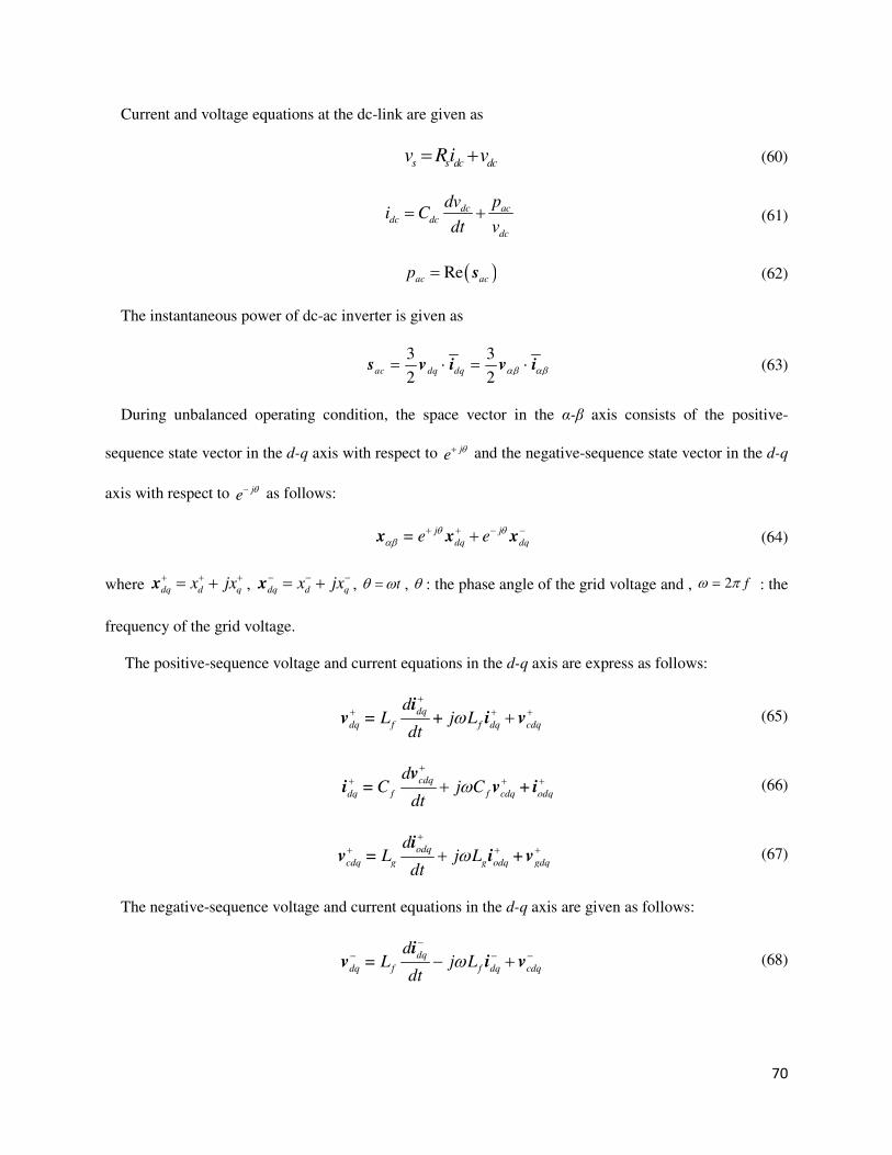
70
Current and voltage equations at the dc-link are given as
s s dc dcv Ri v= + (60)
dc acdc dc
dc
dv pi C
dt v= + (61)
( )Reac acp = s (62)
The instantaneous power of dc-ac inverter is given as
3 3
2 2ac dq dq αβ αβ= ⋅ = ⋅s v i v i (63)
During unbalanced operating condition, the space vector in the α-β axis consists of the positive-
sequence state vector in the d-q axis with respect to je θ+ and the negative-sequence state vector in the d-q
axis with respect to je θ− as follows:
j j
dq dq= e eθ θαβ
+ + − −+x x x (64)
where dq d qx jx+ + += +x , dq d qx jx− − −= +x , tθ ω= , θ : the phase angle of the grid voltage and , 2 fω π= : the
frequency of the grid voltage.
The positive-sequence voltage and current equations in the d-q axis are express as follows:
dq
dq f f dq cdq
d= L + j L
dtω
++ + ++
iv i v (65)
cdq
dq f f cdq odq
d= C j C +
dtω
++ + ++
vi v i (66)
odq
cdq g g odq gdq
d= L j L +
dtω
++ + ++
iv i v (67)
The negative-sequence voltage and current equations in the d-q axis are given as follows:
dq
dq f f dq cdq
d= L j L
dtω
−− − −− +
iv i v (68)

71
cdq
dq f f cdq odq
d= C j C +
dtω
−− − −−
vi v i (69)
odq
cdq g g odq gdq
d= L j L +
dtω
−− − −−
iv i v (70)
5.1.2 Dc power oscillation due to oscillating ac power under grid voltage unbalance
During grid voltage unbalance, ac active and reactive powers of the dc-ac inverter are expressed as
( ) ( )3
2
j t j t j t j t
ac dq dq dq dq ac ace e e e p jqω ω ω ω+ − − + − −= + ⋅ + = +s v v i i (71)
( ) ( )0 2 2cos 2 sin 2ac c sp p p t p tω ω= + + (72)
( ) ( )0 2 2cos 2 sin 2ac c sq q q t q tω ω= + + (73)
From (72) - (73), the dc components and the second order oscillating components of active and reactive
powers are given as follows:
( )0 1.5 d d q q d d q qp v i v i v i v i+ + + + − − − −= + + + (74)
( )2 1.5c d d q q d d q qp v i v i v i v i− + − + + − + −= + + + (75)
( )2 1.5s q d d q q d d qp v i v i v i v i− + − + + − + −= − − + (76)
( )0 1.5 q d d q q d d qq v i v i v i v i+ + + + − − − −= − + − (77)
( )2 1.5c q d d q q d d qq v i v i v i v i− + − + + − + −= − + − (78)
( )2 1.5s d d d q d d q qq v i v i v i v i− + − + + − + −= − − + + (79)
From (60) and (61), the dc power at the dc-link and the ac power of dc-ac inverter are written as
21 1dc dc dc dc s dc
s s
p v i v v vR R
= = − + (80)
21 1 dcac dc s dc dc dc
s s
dvp v v v C v
R R dt= − + − (81)
Based on the small signal modeling, the transfer function from acp% to dcp% is given as

72
( ) dc dcdc
ac dc
pG s
p s
ωω
= =+
%
% (82)
where 2 dc s
dc
dc s dc
V V
V R Cω
−= , sV is a dc term of the dc source voltage, and dcV is a dc term of the dc-link
voltage.
Substituting (65)-(70) into (72), the active power oscillation can be express as
( ) ( )2 2cos 2 sin 2ac c s acp P t P t pω ω= + + ∆% (83)
where acp∆ is the high order terms. 2cP and 2sP are the ac power oscillation coefficients .
And the active power oscillation coefficients are written as follows:
( )( )( )
( )
2 3
1.5
1.5
c g T oq od od oq
f g T C gq oq gd od gq oq gd od
f C gd gq gq gd gd gq gq gd
P Z i i i i
Z Y v i v i v i v i
Y v v v v v v v v
α
α α
α
− + − +
+ − + − − + − +
− + − + + − + −
= −
+ − + + +
+ − + + −
(84)
( )( )( )
( )
2 3
1.5
1.5
s g T od od oq oq
T C f g gq od gd oq gq od gd oq
f C gq gq gd gd gq gq gd gd
P Z i i i i
Z Y v i v i v i v i
Y v v v v v v v v
α
α α
α
− + − +
+ − + − − + − +
− + − + + − + −
= − +
+ − − − +
− + + +
(85)
where 3
T T f g fZ L L L Cω ω= − ,21f f fL Cα ω= − ,
21g g fL Cα ω= − , C fY Cω= , T g fL L L= + .
These results are caused by the modeling of the LCL filter based inverter. In the case of the L filter
based inverter modeling, the ac power oscillation coefficients are the same to (75) and (76) because the
inverter current equals to the output current through L filter. Therefore, conventional current references
are computed by (74) - (79) [101-104]. We need a new current reference in order to remove the dc power
oscillation of the LCL filter based DG inverter from (84) and (85).
The dc power oscillation is a result that the ac power oscillation in (83) passes a low pass filter in (82).
Therefore the high order term, acp∆ , can be filtered and ignored. Since the frequency of the oscillation

73
( 2ω ) is not high enough to be removed, the ac power oscillation coefficients become the dc power
oscillation coefficients as follows:
( ) ( )2 2cos 2 sin 2dc c sp P t P tω ω= +% (86)
If the double d-q frame current controller are applied to regulate unbalanced output current [98],
transfer functions from the d-q axis current references,*
odq
+i and *
odq
−i , to the d-q axis output currents, *
odq
+i
and *
odq
−i are given as
( )*
odq
c
odq
G s
++
+=
i
i, and ( )
*
odq
c
odq
G s
−−
−=
i
i (87)
*
odq
+i( )cG s+
*
odq
−i( )cG s−
( )dcG s
( )cos 2θ
( )sin 2θ
acp∆
acp%dcp%
gαβ+v
gαβ−v
odq
+i
odq
−i2cP
2sP
++
+
je θ− gdq
+v
je θgdq
−v
( )( )
2
2
cos 2
sin 2
dc c
s
p P
P
θ
θ
=
+
%
Fig. 60. Block diagram of the dc power oscillation generation under unbalanced grid voltage.
Fig. 60 shows the block diagram of the dc power oscillation generation under unbalanced grid voltage.
This analysis for a mechanism of the dc power oscillation generation is to minimize the dc power
oscillation of the LCL filter based DG inverter under grid voltage unbalance. If we can find conditions to
remove the dc power oscillation coefficients in (85) and (86), the dc power oscillation, dcp% , will be
rejected. The only way to remove the dc power oscillation is to generate the current references, *
odq
+i and
*
odq
−i . Therefore, it is necessary to find the current references to suppress power oscillation coefficients.

74
5.2 Performance of Conventional Control Scheme
5.2.1 Conventional current reference calculations [98]
The conditions to deliver a constant inverter power without power oscillations of L filter inverter are
given as
( )
( )
( )
( )
2
2
3
2
3
2
30
2
30
2
gd od gq oq gd od gq oq
gq od gd oq gq od gd oq
c d od q oq d od q oq
s q od d oq q od d oq
P v i v i v i v i
Q v i v i v i v i
p v i v i v i v i
p v i v i v i v i
+ + + + − − − −
+ + + + − − − −
− + − + + − + −
− + − + + − + −
= + + + = − + − = + + + = = − − + =
(88)
From (88), the power vector is written with the current components ( odi+, oqi+
, odi− and oqi−
) in the following
matrix expression:
2
2
3
2
gd gq gd gq od
gq gd gq gd oq
c d q d q od
s q d q d oq
P v v v v i
Q v v v v i
P v v v v i
P v v v v i
+ + − − +
+ + − − +
− − + + −
− − + + −
− − =
− −
(89)
By inverting this matrix, it is possible to find the current references to generate active and reactive
powers without active power oscillation under grid voltage unbalance, i.e.
1* *
* *
*
*
2
3 0
0
od gd gq gd gq
oq gq gd gq gd
od gd gq gd gq
oq gq gd gq gd
i v v v v P
i v v v v Q
i v v v v
i v v v v
−+ + + − −
+ + + − −
− − − + +
− − − + +
− − =
− −
(90)
Substituting (90) into (85) and (86), the dc power oscillation can be derived in the L and LCL filter
based inverters.
1) L filter based inverter ( 0fC = )

75
( ) ( )( ) ( )( )
2
2
1.5 1.5
1.5 1.5 0
1.5 0
c gq T od oq gd T od od
oq T od oq gd T oq od
s q od d oq q od d oq
P v Z i i v Z i i
v Z i i v Z i i
P v i v i v i v i
+ + − + + −
− − + − − +
+ − + − − + − +
= + + −
+ − + + =
= − − + =
(91)
Hence, the dc power oscillation is able to be removed as follows:
( ) ( )2 2cos 2 sin 2 0dc c sp P t P tω ω= + =% (91)
2) LCL filter based inverter
The 2cP and 2sP are not canceled as follows:
( ) ( )2 2cos 2 sin 2 0dc c sp P t P tω ω= + ≠% (92)
If the DG inverter is connected with the LCL filter, additional current, which is the capacitor current, is
generated. However, the current reference calculation in (90) is derived by considering the L filter based
inverter, which assumes that the inverter current equals to the output current. Fig. 61 shows simulation
waveforms of dc voltage and dc current oscillation suppression using conventional current reference in
(90). Results show that the dc current and dc voltage oscillations are not reduced under grid voltage
unbalance in the LCL filer based inverter.
Fig. 61. Simulation waveforms of dc voltage and dc current oscillation suppression using conventional current
reference.

76
5.2.3 Conventional double synchronous reference frame current control [98]
Fig. 62 shows the block diagram of conventional d-q frame current control. In order to extract the
positive- and negative-sequence components, either a notch filter at 2ω or an all pass filter can be
implemented. The positive-sequence current controller is designed with a PI regulator. The negative-
sequence current controller is the same to the positive-sequence current controller. The current references
are generated by (90). In order to analyze the dynamic response of conventional d-q frame current control,
the transfer function can be derived from the space vector analysis.
*cdq+v+
+−+
Tj Lωodq+i
gdq+v
*odq+i
+je θ αβv
2
LCL
d
dt
ς
ω
*cαβ+v +
−
*cdq−v+
+−+
Tj Lωodq−i
gdq−v
*odq−i
−je θ−
*cαβ−v
cαβv
j te ω−
j te ω
odq+i
odq−i
oαβi
j te ω−
j te ω
gdq+v
gdq−v
gαβv
oαβ+i
oαβ−i
gαβ+v
gαβ+v
bcSα+
+
Fig. 62. Block diagram of double d-q frame current control.
A space vector, αβx is written as
( ) ( ) ( )j t j t
dq dqt e t e tω ωαβ
+ − −= +x x x (93)
From Appendix C, a skew-symmetric complex operator of positive-sequence is expressed as
( )1ˆ1
2jqαβ
+ = +T (94)
A skew-symmetric complex operator of negative-sequence is expressed as

77
( )1ˆ1
2jqαβ
− = −T (95)
By applying (94) and (95) in (93), the positive- and negative- sequence state vectors in the α-β axis are
computed as
( ) ( ) ( ) ( )( )
( ) ( ) ( ) ( )2 2
1ˆ1
2
1 1ˆ ˆ
2 2
j t j t
dq dq
j jj t j t j t j t
dq dq dq dq
t jq e t e t
e t e qe t e t e qe t
ω ωαβ αβ
π πω ω ω ω
+ + − −
+ + − − − −
= + +
= + + +
T x x x
x x x x
(96)
( ) ( ) ( ) ( )( )
( ) ( ) ( ) ( )2 2
1ˆ1
2
1 1ˆ ˆ
2 2
j t j t
dq dq
j jj t j t j t j t
dq dq dq dq
t jq e t e t
e t e qe t e t e qe t
ω ωαβ αβ
π πω ω ω ω
− + − −
− −+ + − − − −
= − +
= + + +
T x x x
x x x x
(97)
Usually, the skew-symmetric operators in (94) and (95) are implemented by filtering methods such as
the second-order adaptive filter (AF) based on a generalized integrator and the second-order AF based on
a second-order generalized integrator [98]. These approaches are useful to extract symmetrical
components of the grid voltage in the phase look loop (PLL) for the grid synchronization because
response time of the PLL is sufficient with using a low gain in terms of the phase angle of the grid voltage.
However, the second-order filters to extract symmetrical components of the feedback current can affect
the phase margin of the current control loop substantially. Therefore, the first-order all pass filter (APF)
can be used to implement approximated phase-shifting operator.
Transfer function of the APF is given as
( ) sQ s
s
ωω
− +=
+ (98)
The phase-shifting operator based on the APF can be transformed to frequency domain as follows:

78
( ) ( ) ( )2ˆj
j tqe t e Q s s
πθ
ω − →x x (99)
( ) ( ) ( )2ˆj
j tqe t e Q s s
πθ
ω − →x x (100)
By applying (99) and (100) in (96) and (97), frequency responses of the positive- and negative- sequence
state vectors in the in the α-β axis are written as
( ) ( ) ( ) ( ) ( )
( )( ) ( ) ( )( ) ( )
2 22 21 1
2 2
1 11 1
2 2
j jj jj j
dq dq dq dq
j j
dq dq
j j
s e e e Q s s e e e Q s s
e Q s s e Q s s
se e
s s
π ππ πθ θθ θ
αβ αβ
θ θ
θ θαβ αβ
ωω ω
− − − + + + − − −
+ − −
+ − −
= + + +
= + + −
= ++ +
T x x x x x
x x
x x
(101)
( ) ( ) ( ) ( ) ( )
( )( ) ( ) ( )( ) ( )
2 22 21 1
2 2
1 11 1
2 2
j t jj jj j
dq dq dq dq
j j
dq dq
j j
s e e e Q s s e e e Q s s
e Q s s e Q s s
se e
s s
π ππ πω θθ θ
αβ αβ
θ θ
θ θαβ αβ
ωω ω
− − −− − − + + − − −
+ − −
+ − −
= + + +
= − + +
= ++ +
T x x x x x
x x
x x
(102)
Therefore, frequency responses of the positive- and negative- sequence state vectors in the in the d-q axis
are expressed as
( ) ( ) ( ) ( )2ˆ j j
dq dq dq
ss e s s e s
s s
θ θαβ αβ
ωω ω
+ − + + − −= = ++ +
x T x x x (103)
( ) ( ) ( ) ( )2ˆ j j
dq dq dq
ss e s s e s
s s
θ θαβ αβ
ωω ω
− − − += = ++ +
x T x x x (104)
From (103) and (104), the positive- and negative-sequence components in the d-q axis after applying the
phase-shifting operator based on the APF include the response of the first order low pass filter(LPF) as
follows:

79
0
ˆ
odq
odq
odqs
ωω
−
+
+=
+i
i
i, and
0
ˆ
odq
odq
odqs
ωω
+
−
−=
+i
i
i (105)
Fig. 63 shows the simplified double d-q frame current control loop. By applying the active damping
control, the equivalent transfer function from *
cv to cv becomes a second order system. Due to the first
order LPF in (105) for positive- and negative-sequence current components extraction, it will lose the
phase margin in the control loop. Hence, this double d-q frame current controller has a limitation to
achieve high bandwidth.
1
fL s
1
fC s
cdqv+−
+−
2
LCL
d
dt
ς
ω
*cdqv +
−
1
gL s
odqi
2
* 22
cdq LCL
cdq LCL LCLs s
ω
ζω ω+ +
v
v
−
+*odqi
( )PIG s
ˆodqi
s
ωω+
odqi
Fig. 63. Simplified double d-q frame current control loop.
Fig. 64. Step responses of conventional current controllers of L and LC filters based inverter.
Fig. 64 shows step responses of conventional current controllers of L and LC filters based dc-ac
inverters. The response times of controllers are determined by the order of the transfer function with

80
respect to the plant and filter. The conventional d-q frame current controller is designed with the current
using the d-q rotating frame and without filtering in the feedback. The transfer function of L filter based
inverter is the first order system with an integrator form. The LCL filter with active damping is the second
order system as shown in Fig. 63. Thus, the transfer function of LCL filter based inverter becomes the
third order system. The d-q frame current controller of the L filter based inverter in Fig.64 shows the
fastest response time, because there are no feedback filter and the LCL filter in the plant. But the double
d-q frame current controller of the LCL filter based inverter is more difficult to obtain the same response
time of the d-q frame current controller of the L filter based inverter, because it includes the second order
system in the plant as well as the filter in the feedback. Since the double d-q frame current controller is
proposed to regulate the current for the LCL filter based DG inverter under grid voltage unbalance, the
response time of the d-q axis current is limited in terms of the stability vs. bandwidth.
5.3 Proposed Control Scheme for Suppression of DC Power Oscillation
In this section, two methods to minimize the dc power oscillation are proposed. First, an improved
current reference is used to cancel coefficients of the dc power oscillation. Second, a modified reference
frame current control is proposed to overcome the performance limitation of the double d-q frame current
control using the conventional filter approach to extract the positive- and negative-sequence current
components. The proposed control scheme is able to not only regulate the unbalanced output current but
also enhance the bandwidth of controller.
5.3.1 Improved current reference calculation
The conditions to deliver a constant inverter power without power oscillations of LCL filter inverter are
given as
( )
( )( ) ( )2 2 2 2
3
2
3
2
cos 2 sin 2 0 0 and 0
gd od gq oq gd od gq oq
gq od gd oq gq od gd oq
dc c s c s
P v i v i v i v i
Q v i v i v i v i
p P t P t P Pω ω
+ + + + − − − −
+ + + + − − − −
= + + +
= − + − = + ⇔ = =
%
(106)

81
From (84), (85), and (106), the power vector is given with the following matrix:
2
2
0
03 3
2 2
gd gq gd gq od
gq gd gq gd oq
C
gq d gd q gq d gd qd q d q odc
gq q gd d gq qq d q d oqs
v v v v iP
v v v v iQY
v v v v v v v vv v v v iP
v v v v v v vv v v v iP
α α α αα α α α
+ + − − +
+ + − − +
+ − + − − + − +− − + + −
+ − + − − +− − + + −
− − = − − − +
+ + +− − gd dv− +
(107)
where 21g g fL Cα ω= − , C fY Cω= .
By inverting the voltage matrix in (107), new current reference vector is given as follows:
1* *
* *
*
2
*
2
2
3
od gd gq gd gq
oq gq gd gq gd
ffod d q d q c
ffoq q d q d s
i v v v v P
i v v v v Q
i v v v v P
i v v v v Q
α α α αα α α α
−+ + + − −
+ + + − −
− − − + +
− − − + +
− − =
− −
(108)
In order to cancel both dc current and dc voltage oscillations, oscillating power compensation terms are
given as
( )2
3
2
ff
c f gq d gd q gq d gd qP C v v v v v v v vω + − + − − + − += − − + (109)
( )2
3
2
ff
s f gq q gd d gq q gd dP C v v v v v v v vω + − + − − + − += + + + (110)
5.3.2 State Vector under Unbalance Operating Conditions
DG inverters are usually connected to the grid using a three-wire connection without zero-sequence
component. Therefore the zero-sequence component of the voltage vector can be ignored in the equations
presented in this chapter [98].
The state vector in the α-β axis consists of the positive-sequence state vector in the d-q axis and the
negative-sequence state vector in the d-q axis as follows:
( ) ( )1 d d
dq dq
q q
x x x= R R
x x x
α
β
θ θ+ −
−+ −
+
(111)
where dx +, qx+
: positive-sequence components in the d-q axis, and dx −, qx−
: negative-sequence components
in the d-q axis.

82
The d-q transformation with respect to je θ− is defined as
( )cos sin
sin cosdqR
θ θθ
θ θ
= − (112)
Fig. 65 shows the positive- and negative-sequence synchronous reference frames (or d-q frame) in the
α-β axis. The positive-sequence d-q frame is rotated anticlockwise. The negative-sequence d-q frame is
rotated clockwise (Appendix B).
axisα −
axisβ −
O
axis(+)d −
axis(+)q −
axis(-)d −axis(-)q −
Fig. 65. Positive- and negative-sequence synchronous reference frames
From (111) and (112), the state vector in the α-β axis can be organized as
cos
sin
d d q q
q q d d
x x x x x=
x x x x x
α
β
θθ
+ − + −
+ − + −
+ − + + −
(113)
By inverting the matrix in (113), the cosine and sine terms are expressed as
11 12
21 22
cos 1
sin
xa a
xa aD
α
β
θθ
=
(114)
where ( ) ( ) ( ) ( )2 2 2 2
d q d qD x x x x+ + − −= + − − , 11 d da x x+ −= − , 12 q qa x x+ −= − , 21 q qa x x+ −= − − , and
22 d da x x+ −= + .
By using the property of the trigonometric function, the trajectory of the state vector in the α-β axis
becomes a general ellipse equation by the following:

83
2 2Ax Bx x Cx Dα α β β+ + = (115)
where ( )2 2
11 21a aA
D
+= ,
( )11 12 21 222
a a a aB
D
+= ,
( )2 2
12 22a aC
D
+= .
Fig. 66 shows the loci of positive- and negative-sequence state vectors and unbalanced state vector in
the α-β axis. The ellipse is a trajectory by a circle of the negative-sequence vector with clockwise rotation,
traveling along the line of a circle of the positive-sequence vector with anticlockwise rotation.
tθ ω= −
tθ ω=
axisα −
axisβ −
αβ+x
O
αβ−x
αβx
αβ αβ αβ+ −= +x x x
j
dqe θαβ+ +=x x
j
dqe θαβ− − −=x x
Fig. 66. Loci of positive- and negative-sequence sate vectors and unbalanced sate vector in the α-β axis.
From (115) , the Bx xα β term can be eliminated by using the rotation of axes (Appendix D) as follows
formulas:
cos sinx x xα α βφ φ′ = − , and sin cosx x xβ α βφ φ′ = − + (116)
where 11
tan2
d q d q
d d q q
x x x x
x x x xφ
+ − − +−
+ − + −
+= − −
.
Then a standard ellipse equation is transformed as
2 2A x C x Dα β′ ′ ′ ′+ = (117)
where 2 2
cos cos sin sinA A B Cφ φ φ φ′ = + + ,2 2
sin cos sin cosC A B Cφ φ φ φ′ = − + .
Fig. 67 shows the rotation of axes between the general ellipse and the standard ellipse.

84
axisα −
axisβ −
O
φ
axisα ′ −axisβ ′ −
2 2 in the axisAx Bx x Cx Dα α β β α β+ + = −
2 2in the axisA x C x Dα β α β′ ′ ′ ′ ′ ′+ = −
cos sin
sin cos
x x x
x x x
α α β
β α β
φ φ
φ φ
′ ′= − ′ ′= +
Fig. 67. Rotation of axes between general ellipse and standard ellipse.
Moreover, a circle can be obtained by scaling the standard ellipse as follows formulas:
1
x xA
α α′ ′′=′
,1
x xA
β β′ ′′=′
(118)
Then the circle equation is expressed as
2 2x x Dα β′′ ′′+ = (119)
Fig. 68 shows the scaling between the canonical ellipse and the circle.
O axisα ′ −
axisβ ′ −
2 2 in the axisA x C x Dα β α β′ ′ ′ ′ ′ ′+ = −
1
1
x xA
x xA
α α
β β
′ ′′= ′ ′ ′′= ′
axisβ ′′ −
axisα ′′ −
2 2in the axisx x Dα β α β′′ ′′ ′′ ′′+ = −
Fig. 68. Scaling between canonical ellipse and circle.
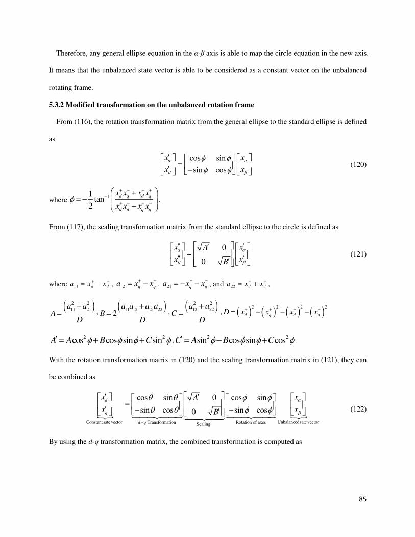
85
Therefore, any general ellipse equation in the α-β axis is able to map the circle equation in the new axis.
It means that the unbalanced state vector is able to be considered as a constant vector on the unbalanced
rotating frame.
5.3.2 Modified transformation on the unbalanced rotation frame
From (116), the rotation transformation matrix from the general ellipse to the standard ellipse is defined
as
cos sin
sin cos
x x
x x
α α
β β
φ φφ φ
′ = ′ −
(120)
where 11
tan2
d q d q
d d q q
x x x x
x x x xφ
+ − − +−
+ − + −
+= − −
.
From (117), the scaling transformation matrix from the standard ellipse to the circle is defined as
0
0
x xA
x xB
α α
β β
′′ ′′ = ′′ ′′
(121)
where 11 d da x x+ −= − , 12 q qa x x+ −= − , 21 q qa x x+ −= − − , and 22 d da x x+ −= + ,
( )2 2
11 21a aA
D
+= ,
( )11 12 21 222
a a a aB
D
+= ,
( )2 2
12 22a aC
D
+= , ( ) ( ) ( ) ( )2 2 2 2
d q d qD x x x x+ + − −= + − −
2 2cos cos sin sinA A B Cφ φ φ φ′ = + + ,
2 2sin cos sin cosC A B Cφ φ φ φ′ = − + .
With the rotation transformation matrix in (120) and the scaling transformation matrix in (121), they can
be combined as
UnbalancedsatevectorConstant satevector Trans Rotation of axesformation Scaling
cos sin 0 cos sin
sin cos sin cos0
d
q
d q
x xA
x xB
α
β
θ θ φ φθ θ φ φ
−
′ ′ = ′ − −′ 1442443 14424431442443
(122)
By using the d-q transformation matrix, the combined transformation is computed as

86
( ) ( ) ( )
( ) ( )
( ) ( )
2 1
2 1
0
0
cos sin
sin cos
dq dq dq
AT = R R
C
C
AA
C
A
θ θ φ
θ φ θ φ
θ φ θ φ
′′
′
+ +
= − + +
(123)
From (123), we define a new δ-γ transformation matrix as follows:
( ) ( ) ( )( ) ( )
2 1
2 1
cos sin, ,
sin cosi
kU k =
kδγ
θ φ θ φφ θ
θ φ θ φ+ +
− + + (124)
The inverse transform matrix is expressed as
( )( )
( ) ( )
( ) ( )
1 11
1 2 2 2
cos sin1
, , 1 1cos sin cos
iU k =
k k
δγ
θ φ θ φφ θ
φ φ θ φ θ φ−
+ − + − − + +
(125)
The unbalance factors, k , 1φ , and 2
φ , are defined as follows:
( ) ( )( ) ( )
2 2
2 2
d d q q
q q d d
x x x xk
x x x x
+ − + −
+ − + −
+ + −=
+ + − (126)
1
1tan
q q
d d
x x
x xφ
+ −−
+ −
−= +
, and 1
2tan
q q
d d
x x
x xφ
+ −−
+ −
+= −
(127)
From (113), the state vector in the α-β axis can be organized as
( ) ( )( ) ( )
cos sin
cos sin
d d q q
q q d d
x x x xx=
x x x x x
α
β
θ θ
θ θ
+ − − +
+ − + −
+ + − + + −
(128)
Then, it can be rewritten as
( )
( )
1
2
cos
sin
Xx
Xx
k
α
β
θ φ
θ φ
+ = +
(129)

87
In (129), the constant state vector in the δ-γ axis is expressed by the positive- and negative-sequence state
vectors in the d-q axis as follows:
( ) ( ) ( ) ( )2 2
1 2cos, ,
0
d d q qi
x x x x x x=U k
x x
δ αδγ
γ β
φ φφ θ+ − + − + + − − =
(130)
The δ-γ axis is the modified d-q axis on the unbalanced rotating frame. Then the unbalanced state vector
in the α-β axis is transformed to constant state vector in the δ-γ axis.
t
xδ
xγ
( )dqR θ
( )dqR θ−
t
dx+
qx+
t
1 2, , kφ φ
αβx
αβ+x
αβ−x
dx−
qx−
axisβ −
O axisα −O
axis(+)d −
axis(+)q −
axis(-)d −axis(-)q −
( ), ,iU kδγ φ θ
Fig. 69. Comparison between the δ-γ transformation and the d-q transformation under unbalanced operating
conditions
Fig 69 shows the comparison between the δ-γ transformation and the d-q transformation under
unbalanced condition. The locus of unbalanced state makes the ellipse in the α-β axis in (115). The
positive- and negative-sequence state vectors draw circles in (117). Unbalance factors ( k , 1φ , and 2
φ ) are
derived by the positive- and negative-sequence components in (126) and (127). With unbalanced factors,
the δ-γ transformation makes a constant state vector in the δ-γ axis. This means that unbalanced state
vector in the α-β axis is able to make constant state vector in (130). It includes positive- and negative-
sequence components in the d-q axis without tθ ω= .
5.3.3 Dynamic voltage equation on the unbalanced rotating frame
The voltage equation with the active damping controller in the α-β axis can be approximated as

88
o
c T g
dL
dt
αβαβ αβ= +
iv v (131)
To apply the voltage equation in the α-β axis, the δ-γ transformation is defined as
( )( ) ( )( ) ( )
* * *
2 1* *
* * *
2 1
cos sin, ,
sin cosi
kU k
kδγ
θ φ θ φφ θ
θ φ θ φ
+ + = − + +
(132)
where ( ) ( )( ) ( )
2 2* * * *
*
2 2* * * *
od od oq oq
oq oq od od
i i i ik
i i i i
+ − + −
+ − + −
+ + −=
+ + −,
* *
* 1
1 * *tan
oq oq
od od
i i
i iφ
+ −−
+ −
−= +
,
* *
* 1
2 * *tan
oq oq
od od
i i
i iφ
+ −−
+ −
+= −
, and the *
odi+,
*
oqi+,
*
odi−,
and *
oqi− are the current references computed by (108)-(110) to minimize the dc voltage and dc current
oscillations.
By applying the δ-γ transformation in (131), the voltage equation is expressed as
( ) ( ) ( )* * * * * *, , , , , ,gc o
i T i i
gc o
vv idU k L U k U k
vv idt
αα αδγ δγ δγ
ββ β
φ θ φ θ φ θ
= +
(133)
From (133), the voltage equation in the δ-γ axis is given as
( ) ( ) ( )
( ) ( )
* * 1 * * * *
* * 1 * *
Decoupling term
, , , , , ,
, , , ,
gc o
T i i i
gc o
go o
T T i i
go o
vv idL U k U k U k
vv idt
vi id dL L U k U k
vi idt dt
δδ αδγ δγ δγ
γγ β
δδ δδγ δγ
γγ γ
φ θ φ θ φ θ
φ θ φ θ
−
−
= +
= + +
14444444244444443
(134)
Since unbalance factors, *k and *
iφ , are computed by the current references, they are independent to the
feedback current in terms of dynamic state vector. Hence, the derivative of the unbalance factors can be
ignored, then
**
0, and 0iddk
dt dt
φ= = (135)
By computing the derivative of the δ-γ transformation, the decoupling term in (134) becomes as

89
( ) ( )( )
( )
* *
1 2* * 1 * *
* *
1 2
tan 1, , , ,
1 tani i
dU k U k
dtδγ δγ
φ φφ θ φ θ ω
φ φ−
− − = − −
(136)
From (134) and (136), a new voltage equation in the δ-γ axis is written as
( )( )
* **1 2
* * *
1 2
tan 1
1 tan
gc o o
T T
gc o o
vv i idL L
vv i idt
δδ δ δ
γγ γ γ
φ φω
φ φ
− − = + + − −
(137)
Based on this voltage equation, the δ-γ frame current control is designed with decoupling and
feedforward compensations. However, the grid voltage does not become a constant state vector in the δ-γ
axis because the δ-γ transformation is oriented by the current reference vector. The grid voltage in the α-β
axis can be express as
( )
( )
1
2
cos
sin
mg
mg
Vv
Vv
k
α
β
θ φ
θ φ
+ = +
(138)
where ( ) ( )( ) ( )
2 2
2 2
gd gd gq gq
gq gq gd g d
v v v vk
v v v v
+ − + −
+ − + −
+ + −=
+ + −,
1
1tan
gq gq
gd gd
v v
v vφ
+ −−
+ −
−= +
, 1
2tan
gq gq
gd gd
v v
v vφ
+ −−
+ −
+= −
.
The unbalance factors, *k and *
iφ , in the output current are not equal to the unbalance factors , k and
iφ ,in the grid voltage as follows:
* * *
1 1 2 2, , andk k φ φ φ φ≠ ≠ ≠ (139)
Therefore, the grid voltage in the δ-γ axis becomes a function of 2 tω , i.e.
( )( )
( )
( )
( )
1* *
2
* ** * *
1 2 1 2 1 2
* ** * *
1 2 1 2 1 2
cos
, ,sin
1 cos cos(2 ) cos(2 )
21 sin sin(2 ) sin(2 )
mg
im
g
m
Vv
=U k Vvk
k k
k kV
k k
k k
δδγ
γ
θ φφ θ
θ φ
φ φ θ φ φ θ φ φ
φ φ θ φ φ θ φ φ
+ +
+ − + + + − + +
= − − − + + + + +
(140)

90
Fig. 70 shows the loci of unbalanced current and voltage state vectors in the α-β axis. They are
orthogonal but asymmetrical. In the view of the δ-γ transformation with the output current vector, the
result of the δ-γ transformation with the grid voltage vector is oscillated with 2ω .
axisα −
axisβ −
t
2ω
t
gv δ
oi δ
O
gv δ
oi γ
oαβi
( ), ,iU kδγ φ θ oδγi
gαβv( ), ,iU kδγ φ θ gδγv
Fig. 70. Loci of unbalanced current and voltage vectors in the α-β axis.
5.3.4 Unbalanced grid voltage compensation on the unbalanced rotating frame
Fig. 71 shows the block diagram of current control loop in the δ-γ axis. Based on the δ-γ
transformation, the feedback current becomes a constant state. The equivalent plant in the δ-γ axis has the
δ-γ axis grid voltage oscillation in (140). To cancel this disturbance, the feedforward term is compensated.
However, the feedforward term is difficult to cancel the δ-γ axis grid voltage exactly because there is the
LCL filter with active damping. The oscillation term is delayed because of the second order system that is
equivalent to the transfer function of the LCL filter with active damping.
−
+*oδγi
( )PIG s1
TsL
2
22
LCL
LCL LCLs s
ω
ζω ω+ +
( )2j
g mV eθ φ
δγ+=%v
( )2ˆ jff
g mV eθ φ
δγ+=%v
−++
+
( )2ˆ LCLj
mV eθ φ φ+ −
t
oδγi
t
2ωgδγv
Fig. 71. Block diagram of current control loop in the δ-γ axis.

91
Fig. 72 shows the Bode plot of the LCL filter with active damping. Based on the frequency response,
the phase response, LCLφ , is 7.82° at 2ω (120Hz). This means that the δ-γ axis grid voltage in (140) is
delayed with 7.82° phase response if the feedforward compensation is applied in the controller. The value
of delayed phase is able to be computed from the frequency analysis of the second order system of the
LCL filter with active damping.
Fig. 72. Bode plot of LCL filter with active damping.
The frequency response of LCL filter with active damping is given as
( )2
2 22
22
LCLLCL s j
LCL LCL s j
G ss sω
ω
ωζω ω=
=
=+ +
(141)
where f g
LCL
f g f
L L
L L Cω
+= , 0.707ζ .
Then the phase response of LCL filter with active damping at 2ω (120Hz) is computed as
31
2 2 4
4tan
4
LCLLCL
LCL LCL
ζω ωφ
ω ω ω−
= − (142)
From (128), the modified feedforward vector with the phase compensation is given as
( )* *, ,
ff
g g
i LCLff
g g
v v= U k
v v
δ αδγ
γ β
φ θ φ
+
(143)

92
5.3.5 Proposed control scheme
Fig. 73 shows the proposed control block diagram for the dc power oscillation suppression. The
proposed d-q current reference matrix in (108)-(110) computes the positive- and negative-sequence
current references in the d-q axis. By using the d-q current reference, the δ-γ axis current reference is
given as
( ) ( ) ( )2 2* * * * * * *
1 2*
cos
0
o od od oq oq
o
i i i i i
i
δ
γ
φ φ+ − + − + + − − =
(144)
The unbalance factors and transformation are given in (132). The δ-γ frame current controller regulates
the δ-γ axis current with respect to the unbalanced current in the α-β axis with the decoupling and
feedforward compensations. In addition, the feedforward term in (143) compensates the δ-γ axis grid
voltage with the phase delay.
*oi δ
*oi γ
ffgv δ
ffgv γ
oi δ
oi γ
*cαβv
*αβv
abcS
dq+
v
dq−
v
αβv
αβ+v
αβ+v
( )dqR θ
+−
+
−
+
+
+
−
*P
*Q
dq+v
dq−
v
gdq+v ( )
1* *
* *
*
2
*
2
2
2
3
2
3
2
3
2
od gd gq gd gq
oq gq gd gq gd
ffod d q d q c
ffoq q d q d s
ff
c f gq d gd q gq d gd q
ff
s
i v v v v P
i v v v v Q
i v v v v P
i v v v v Q
P C v v v v v v v v
P
α α α αα α α α
ω
ω
−+ + + − −
+ + + − −
− − − + +
− − − + +
+ − + − − + − +
− − =
− −
= − − +
= ( )f gq q gd d gq q gd dC v v v v v v v v+ − + − − + − ++ + +gdq−
v
*odi+
*odi−
*oqi−
*oqi+
*k
*1φ
*2φ
( ) ( ) ( )
( ) ( )( ) ( )
2 2* * * * * * *
1 2*
2 2* * * *
*
2 2* * * *
* * * *
* 1 * 1
1 2* * * *
cos
0
tan , tan
o od od oq oq
o
od od oq oq
oq oq od od
oq oq oq oq
od od od od
i i i i i
i
i i i ik
i i i i
i i i i
i i i i
δ
γ
φ φ
φ φ
+ − + −
+ − + −
+ − + −
+ − + −− −
+ − + −
+ + − − =
+ + −=
+ + −
− += = + −
*oi δ
*oi γ
TLω
TLω
( )1 2tanTLω φ φ−
( )1 2tanTLω φ φ−
+
+
( )1 * *, ,iU kδγ φ θ−
*k*1φ *
2φ
oδγi
ffgδγv
( )* *, ,iU kδγ φ θ
*k*1φ *
2φ
( )LCLUδγ θ φ+
*k*1φ *
2φ
oαβi
gαβv
( )dqR θ−
gdq+v
gdq−
v
gαβ+v
gαβ+
v
( )dqR θ
( )dqR θ−
++−
+
gαβv
gqv+
tθ ω=
Fig. 73. Proposed control block diagram for dc power oscillation suppression.

93
5.4 Simulation Results
In order to validate the proposed control scheme, simulation is performed in Matlab. The unbalanced
grid voltage occurs from 0.15s to 0.25s.
Fig. 74 shows simulation waveforms of d-q axis output current, dc voltage, and dc current with
conventional and proposed control schemes. With conventional control approach, the dc voltage and dc
current in terms of dc power are not regulated under unbalanced grid voltage, although the double d-q
frame current loops are operated. On the other hand, in the proposed control approach, the dc voltage and
dc current are regulated with constant values under grid voltage unbalance. Compared with the transient
response time of the d-q axis output currents, the proposed control approach is faster than the
conventional control approach.
Fig. 74. Simulation waveforms of d-q axis output current, dc voltage, and dc current with conventional
and proposed control schemes.
Fig. 75 shows simulation waveforms of the α-β axis current and the δ-γ axis current of proposed control
scheme. The output current in the α-β axis is balanced from 0.1s to 0.15s and from 0.25s to 0.3s. The
unbalanced current is generated from 0.15s to 0.25s because the controller is regulating to provide
constant active power of the inverter under grid voltage unbalance. The loci of the α-β axis current is
changed from a circle under balanced operating condition to an ellipse under unbalanced operating

94
condition. However the δ-γ axis current is always constant without oscillation because the δ-γ
transformation makes constant state on unbalanced operating frame.
Fig. 76 shows simulation waveforms of three phase voltage, current, and dc power after applying the
proposed controller under grid voltage unbalance. By using the proposed current reference, there is no dc
power oscillation during unbalanced grid voltage.
Fig. 75. Simulation waveforms of the α-β axis current and the δ-γ axis current of proposed control scheme.
Fig. 76. Simulation waveforms of three phase voltage, current, and dc power of proposed control scheme.

95
5.5 Experimental Results
Fig. 77 shows the experimental setup of hardware in the loop using RTDS and dSPACE. Power switch
circuits including the DG inverter, LCL filter, step-down transformer connecting to the main power grid,
and other power components are built in RSCAD. They are emulated in the RTDS. The proposed current
control algorithm was implemented by the digital controller using the DSP control board
(TMS320F28335). All PWM signals are transmitted RTDS through GTDI card. All voltage and current
signals are measured from the output of GTAO card. The dSPACE generates the current reference based
on (108).
Fig. 77. Experimental setup of hardware in the loop using RTDS and dSPACE.
Fig. 78 shows experimental waveforms of conventional current control under balanced grid voltage.
Fig. 79 shows experimental waveforms of conventional current control under unbalanced grid voltage.
The conventional dual current control with current reference in (90) cannot remove the dc current and dc
voltage’s ripples under unbalanced grid voltage conditions. Fig. 80 shows experimental waveforms of
proposed current control under unbalanced grid voltage. The proposed current control shows that the dc
current and dc voltage’s ripples are minimized under unbalanced grid voltage condition. Therefore,
simulation and experimental results verified that the proposed control method can minimize the dc power
ripple under unbalanced operating conditions.

96
Fig. 78. Experimental waveforms of conventional control under balanced grid voltage.
Fig. 79. Experimental waveforms of conventional control under unbalanced grid voltage.
Fig. 80. Experimental waveforms of proposed control under unbalanced grid voltage.
97
5.6 Conclusion
This chapter proposed an enhanced control scheme of the LCL filter based DG inverter under grid
voltage unbalance. The unbalanced grid voltage is reflected by a dc power oscillation to the dc source
side. To minimize this oscillation, the double d-q frame current control schemes have been proposed.
However, the conventional d-q frame current control was limited only in the case of the L filter based
inverter. Therefore, the enhanced reference calculation was derived. By using new δ-γ transformation, the
δ-γ frame current controller enables regulation of a constant current in the δ-γ axis as well as improvement
of the bandwidth of the controller. With δ-γ axis current loops, the dc power oscillation was suppressed
effectively. The proposed control strategy could reduce the impact of the renewable energy under grid
voltage unbalance. As a result, constant dc power generation will also enhance the stability, and reliability
of renewable energy sources. Simulation and experimental results verified that the proposed control
method is able to minimize the dc power oscillation effectively under unbalanced operating conditions.

98
CHAPTER 6. SUMMARY AND FUTURE WORK
This dissertation proposed diverse control strategies for power electronic converters in order to
improve the control performance of a dc-dc converter under different operation modes and a DG inverter
under different operation modes and unbalanced operating conditions. It is summarized as follows:
1) A seamless control scheme for the dc-dc converter application with different operation modes is
proposed to make mode transitions between DCM and CCM seamlessly by adding a mode tracker, and
then the boost converter can smoothly operate by mixing the voltage and current control loop in both
operation modes.
2) A seamless control scheme for the DG inverter application with different operation modes is
proposed to make fast and stable mode transition technologies. The proposed approach is based on a
current controller and a feedforward voltage controller to minimize the grid overvoltage and to improve
the response time.
3) A modified reference frame based current control with improved current reference for the DG
inverter application under grid voltage unbalance is proposed to minimize the dc voltage and dc current
oscillations. With the proposed approach, the dc power oscillation is reduced effectively.
On the other hand, additional control approaches with proposed methods will be needed to improve the
performance of proposed control strategies under other conditions. Future work is suggested as follows:
1) Proposed seamless control strategy of dc-dc converters is applied in the boost converter. This control
scheme is able to be applied in other dc-dc converters such as buck converters. The dynamics analysis of
CCM and DCM of the buck converter is necessary to apply to the buck converter.
2) Proposed seamless control strategy for DG inverters is considered with overvoltage condition. In
order to extend the proposed control approach, the analysis of under voltage conditions will be needed to
guarantee the control stability of the proposed seamless control.
3) The current reference calculation and unbalanced current control method of the LCL filter based DG
inverter is considered under grid voltage unbalance without harmonics. However, the performance of the
proposed unbalanced current controller is limited to reduce the current distortion under grid voltage

99
unbalance and harmonics. As future work, a multiple synchronous reference frame based current control
scheme will be considered to enhance the performance of the unbalanced current control scheme.

100
PUBLICATIONS
1) Journal
[1] Tai-Sik Hwang; Sung-Yeul Park; "Seamless Boost Converter Control Under the Critical Boundary Condition
for a Fuel Cell Power Conditioning System," IEEE Transactions on Power Electronics, vol.27, no.8, pp.3616-
3626, Aug. 2012
[2] Tai-Sik Hwang; Tarca, M.J.; Sung-Yeul Park; "Dynamic Response Analysis of DC–DC Converter With
Supercapacitor for Direct Borohydride Fuel Cell Power Conditioning System,", IEEE Transactions on Power
Electronics, vol.27, no.8, pp.3605-3615, Aug. 2012
[3] Tai-Sik Hwang; Sung-Yeul Park, "A Seamless Control Strategy of a Distributed Generation Inverter for the
Critical Load Safety Under Strict Grid Disturbances," Power Electronics, IEEE Transactions on , vol.28, no.10,
pp.4780,4790, Oct. 2013
2) Conference
[4] Tai-Sik Hwang; Sung-Yeul Park; , "Seamless boost converter control in critical boundary condition for fuel cell
power conditioning system," Energy Conversion Congress and Exposition (ECCE), 2011 IEEE , vol., no.,
pp.3641-3648, 17-22 Sept. 2011
[5] Tai-Sik Hwang, Matthew J. Tarca and Sung-Yeul Park, “Dynamic Response Analysis of DC-DC Converter
with Supercapacitor for Direct Borohydride Fuel Cell Power Conditioning System”, 8th International
Conference on Power Electronics - ECCE Asia, May 30-June 3, 2011, The Shilla Jeju, Korea
[6] Matthew J. Tarca, Tai-Sik Hwang, and Sung-Yeul Park, “Design and Operation of an Autonomous Fuel Cell-
Supercapacitor Power System for Portable Applications”, 8th International Conference on Power Electronics -
ECCE Asia, May 30-June 3, 2011, The Shilla Jeju, Korea
[7] Tai-Sik Hwang; Sung-Yeul Park; , "A seamless control strategy of distributed generation inverter for critical
load safety under strict grid disturbance," Applied Power Electronics Conference and Exposition (APEC), 2012
Twenty-Seventh Annual IEEE , pp.254-261, 5-9 Feb. 2012
[8] Tai-Sik Hwang; Sung-Yeul Park; "DC Power Ripple Minimization of LCL filter based Distributed Generation
Inverter under Unbalanced Voltage Conditions," Applied Power Electronics Conference and Exposition
(APEC), 2013

101
APPENDIX A. MODELING OF THEREE PHASE LCL FILTER BASED DC-AC
INVERTER
A.1 Dc-ac inverter modeling in the abc axis
fL
av
gL
fC
aicav
dcv
dcC bv
cv
bi
ci
cbv
ccv
oai
obi
oci
gav
gbv
gcv
Fig. 81. Circuit diagram of three phase LCL filter based dc-ac inverter
Voltage and current equation in the abc axis are expressed as
abcabc f cabc
cabcabc f oabc
oabccabc g oabc
d= L +
dt
d= C
dt
d= L +
dt
+
iv v
vi i
iv v
(A-1)
where fL : the filter inductor, fC :the filter capacitor, gL :the gird inductor, [ ]T
abc a b cv v v=v : the
inverter voltage, [ ]T
cabc ca cb ccv v v=v : the capacitor voltage, T
gabc ga gb gcv v v = v : the grid
voltage, [ ]T
abc a b ci i i=i : the inverter current, and [ ]T
oabc oa ob oci i i=i : the output current.
A.2 α-β / d-q dc-ac inverter modeling using a vector notation
To transform the abc axis variables to the α-β axis variables, the α-β transformation matrix is given as

102
1 11
2 2 2
3 3 30
2 2
abcαβ
− −
=
−
r rx x (A-2)
where T
x xαβ α β = rx , and
T
abc a b cx x x= rx .
The α-β transformation matrix is invariant to time. By applying (A-2) in (A-1), the voltage and current
equations in the α-β axis are expressed as
f c
c
f o
o
c g o
d= L +
dt
d= C
dt
d= L +
dt
αβαβ αβ
αβαβ αβ
αβαβ αβ
+
rr r
rr r
rr r
iv v
vi i
iv v
(A-3)
where T
v vαβ α β = rv : the α-β axis inverter voltage,
T
c c cv vαβ α β = rv : the α-β axis capacitor
voltage, T
g g gv vαβ α β = rv : the α-β axis grid voltage,
T
i iαβ α β = ri : the α-β axis inverter current, and
T
o o oi iαβ α β = i : the α-β axis output current.
To transform the α-β axis variables to the to the d-q axis variables, the d-q transformation matrix is given
as flows:
( )cos sin
sin cosdqR
θ θθ
θ θ
= − (A-4)
cos sin
sin cosdq αβ
θ θθ θ
= −
r rx x (A-5)
where T
dq d qx x = x , and T
x xαβ α β = x .
The derivative of the α-β axis state vector with the d-q transformation matrix become as
( ) ( ) ( ) ( ) ( ) ( )( )1 1dq dq dq dq dq dq dq
d q vector
d d dR R R R R R
dt dt dt
αβαβθ θ θ θ θ θ− −
−
= =
rr r
14243
xx x (A-6)

103
( ) ( )( ) ( ) ( )( )1 1 dq
dq dq dq dq dq dq
dd dR R R R
dt dt dtθ θ θ θ− −= +
rr r xx x (A-7)
The derivative of the inverse d-q transformation matrix is expressed as
( )( )1 sin cos
cos sindq
dR
dt
θ θθ ω
θ θ− − −
= − (A.8)
Then, we can obtain as follows:
( ) ( )( )1 cos sin sin cos 0 1
sin cos cos sin 1 0dq dq
dR R
dt
θ θ θ θθ θ ω ω
θ θ θ θ− − − −
= = − − (A-9)
We can define the following matrix as
0 1
1 0J
− =
(A-10)
Therefore, (A.6) is given as
( ) dq
dq dq
ddR J
dt dt
αβθ ω= +
rrrxxx (A-11)
From (A-11) and (A-3), the voltage and current equations in the d-q axis are expressed as
dq
dq f dq cdq
cdq
dq f cdq odq
odq
cdq g odq o
d= L +J
dt
d= C J
dt
d= L +J
dtαβ
ω
ω
ω
+
+ +
+
rrr r
rr rr
rrr r
iv i v
vi v i
iv i v
(A.12)
A.3 α-β / d-q dc-ac inverter modeling using a complex space vector notation
To transform the abc axis variables to the to the α-β axis variables, the α-β transformation matrix is given
as
( )2 /3 4 /32
3
j ja b cx jx x x e x eπ π
αβ α β= + = + +x (A.13)

104
f c
c
c f o
o
c g o
d= L +
dt
d=C
dt
d= L +
dt
αβαβ αβ
αβαβ αβ
αβαβ αβ
+
iv v
vi i
iv v
(A.14)
To transform the α-β axis variables to the to the α-β axis variables, the d-q transformation operator is
given as
( ) jdqR e θθ −= (A.15)
jdq e θ
αβ−=x x (A.16)
where dq d qx jx= +x .
The derivative of the α-β axis state vector with the d-q transformation operator become as
( )j j j j j jdq
d q vector
d d de e e e e e
dt dt dt
αβθ θ θ θ θ θαβ
− − − −
−
= =
14243
xx x (A.17)
( ) ( ) dqj j j jdq dq
dd de e e e
dt dt dt
θ θ θ θ− −= +x
x x (A.18)
Then, we can obtain as follows:
( )j jde e j
dt
θ θ ω− = (A.19)
Therefore, (A.14) is given as
dqjdq
dde j
dt dt
αβθ ω− = +xx
x (A.20)
From (A-20) and (A-14), the voltage and current equations in the d-q axis are expressed as
dq
dq f dq cdq
cdq
dq f cdq odq
odq
cdq g odq o
d= L + j
dt
d= C j
dt
d= L + j
dtαβ
ω
ω
ω
+
+ +
+
iv i v
vi v i
iv i v
(A.21)

105
From either (A.12) or (A.21), the stat space equation in the d-q axis for the LCL filter based dc-ac
inverter is given as
dA B E
dt= + +
xx u w (A.21)
where T
d q cd cq od oqi i v v i i = x : the state variables, T
d qv v = u : the control input,
T
gd gqv v = w : the disturbance,
0 / 1 0 0 0
/ 0 0 1 0 0
0 0 0 / 1 0
0 0 / 0 0 1
0 0 0 0 0 /
0 0 0 0 / 0
f
f
f
f
g
g
L
L
CA
C
L
L
ωω
ωω
ωω
− −
= −
,
1/ 0
0 1/
0 0
0 0
0 0
0 0
f
f
L
L
B
=
, and
1/ 0
0 1/
0 0
0 0
0 0
0 0
g
g
L
L
E
=
.

106
APPENDIX B. GENERAL COMPLEX SPACE VECTOR
A general space vector, αβx , in the α-β axis is express with a summation of the nth order positive-sequence space
vectors ,n
αβ+x , in the α-β axis and the nth order negative-sequence space vectors,
n
αβ−x , in the α-β axis. And it is
expressed by a summation of the nth order positive-sequence d-q axis space vectors,n
dq
+x , with jne θ and the nth
order negative-sequence d-q space vectors, n
dq
−x ,with respect to jne θ− . The general space vector is written as
( )
( )1,2,3,
1,2,3,
n n
n
jn n jn n
dq dq
n
e e
αβ αβ αβ
θ θ
+ −
=
+ − −
=
= +
= +
∑
∑
L
L
x x x
x x
(B-1)
Fig. 82. Loci of space vectors in the α-β axis and their waveforms in time domain.
Fig. 82 shows the loci of the nth order space vectors in the α-β axis and their waveforms in time
domain.

107
APPENDIX C. SYMMETRICAL COORDINATE ANALYSIS
Based on the conventional symmetrical coordinate method [98], there are skew-symmetric
transformation matrices to extract the positive-sequence components and the negative-sequence
components in the α-β axis, i.e.
ˆ11
ˆ 12
qT
qαβ+ −
=
, and ˆ11
ˆ 12
qT
qαβ−
= − (C-1)
where 2ˆj
q eπ
−= is a 90˚-lagging phase-shifting operator applied on the time domain to obtain an in-
quadrature version of the input waveforms [98].
The phase-shifting operator, q , is a mathematical operator to make the phase shifting of the input
waveform as follows:
ˆ , 1, 2,3,2
n nq n t nπ
ω = − =
Lx x (C-2)
From (C-1), skew-symmetric operators with the phase-shifting operator are defined as
( )1ˆ1
2jqαβ
+ = +T , and ( )1ˆ1
2jqαβ
+ = −T (C-3)
By applying the skew-symmetric operators, a summation of the positive-sequence space vectors and
a summation of the negative-sequence space vectors are extracted as
1,2,3,
1,2,3,
n jn
dq
n
n jn
dq
n
e
e
θαβ αβ
θαβ αβ
+ + +
=
− − −
=
=
=
∑
∑
L
L
T x x
T x x
(C-4)
A band pass operator is defined as follows:

108
,
0,
n
n k if n k
if n k
==
≠
xG x (C-5)
Using the band pass operator, the nth-order positive- and negative- sequence space vectors in the α-β
axis are expressed as
n n jn
dq
n n jn
dq
e
e
θαβ αβ
θαβ αβ
+ +
− − −
=
=
G T x x
G T x x (C-6)
where 1,2,3,n = L .
Using the d-q transformation, the nth-order positive- and negative- sequence space vectors in the d-q
axis can be extracted as follows:
ˆ
ˆ
n jn n
dq
n jn n
dq
e
e
θαβ
θαβ
+ − +
− −
=
=
x x
x x (C-7)
These results are the representation of the complex space vector to compute the positive- and negative-
sequence components based on multiple d-q frames.

109
APPENDIX D. ROTATION OF AXES [135]
A general equation of the conic is given as
2 20Ax Bxy Cy Dx Ey F+ + + + + = (D-1)
To eliminate the xy-term in (D-1), a procedure called rotation of axes is used as follows.
( ),P x y′ ′=
x
y
O
θ
x′y′
α θ−
Fig. 83. Rotation of axes
From Fig. 83, using the formulas for the sine and cosine of the difference of two angles, we can obtain
as
( )( )
cos cos cos sin sin cos sin
sin sin cos cos sin sin sin
x r r r x y
y r r r y x
α θ α θ α θ θ θ
α θ α θ α θ θ θ
′ = − = + = +
′ = − = − = − (D-2)
where , cosx r α= , and siny r α= .
Solving (D-2), the coefficients of the new equation are obtained by making the substitutions
cos sin
sin cos
x x y
y x y
θ θθ θ
′ ′= − ′ ′= +
(D-3)
By substituting (D-3) into (D-1), we can obtain as follows:

110
2 2
2 2
cos cos sin sin
sin cos sin cos
cos sin
sin cos
A A B C
C A B C
D D E
E D E
F F
θ θ θ θ
θ θ θ θθ θθ θ
′ = + +
′ = − + ′ = + ′ = − +
′ =
(D-4)
In order to eliminate the x′ and y′ terms, we need to choose θ such that 0B′ = , as follows:
( ) ( )( )
( )
2 22 sin cos cos sin
sin 2 cos 2
sin 2 cot 2 0
B C A B
C A B
C AB
B
θ θ θ θ
θ θ
θ θ
′ = − + −
= − +
− = + =
(D-5)
where sin 2 0θ ≠ .
If 0B = , there is no rotation, because the xy-term is included in (D-1), In the case of 0B ≠ , we have
the condition to make 0B′ = as follows:
cot 2 , 0A C
BB
θ−
= ≠ (D-6)
By rotating the coordinate axes in (D-3) through the angle,θ , in (D-6), a standard equation of the
conic is given as
2 20A x Cy Dx E y F′ ′ ′ ′ ′+ + + + = (D-7)

111
REFERENCES
[1] X. Zhou, S. –Y. Park, “Design and analysis of a direct borohydride fuel cell dc-dc converter for
portable applications,” Proc. of ASME 2010 8th international fuel cell science 7 technology
conference, 14-16 Jun. 2010, Brooklyn NY.
[2] Itoh, J.-i.; Hayashi, F.; , "Ripple Current Reduction of a Fuel Cell for a Single-Phase Isolated
Converter Using a DC Active Filter With a Center Tap," Power Electronics, IEEE Transactions on ,
vol.25, no.3, pp.550-556, March 2010
[3] Changrong Liu; Jih-Sheng Lai; , "Low Frequency Current Ripple Reduction Technique With Active
Control in a Fuel Cell Power System With Inverter Load," Power Electronics, IEEE Transactions on ,
vol.22, no.4, pp.1429-1436, July 2007
[4] Kyung-Won Suh; Stefanopoulou, A.G.; , "Coordination of Converter and Fuel Cell Controllers,"
Intelligent Control, 2005. Proceedings of the 2005 IEEE International Symposium on, Mediterrean
Conference on Control and Automation, pp.563-568, 27-29 June 2005.
[5] Qian, Z.; Abdel-Rahman, O.; Batarseh, I.; , "An Integrated Four-Port DC/DC Converter for
Renewable Energy Applications," Power Electronics, IEEE Transactions on , vol.25, no.7, pp.1877-
1887, July 2010.
[6] Samosir, A.S.; Yatim, A.H.M.; , "Implementation of Dynamic Evolution Control of Bidirectional
DC–DC Converter for Interfacing Ultracapacitor Energy Storage to Fuel-Cell System," Industrial
Electronics, IEEE Transactions on , vol.57, no.10, pp.3468-3473, Oct. 2010
[7] Liu, W.; Chen, J.; Liang, T.; Lin, R.; Liu, C.; , "Analysis, Design, and Control of Bidirectional
Cascaded Configuration for a Fuel Cell Hybrid Power System," Power Electronics, IEEE
Transactions on , vol.25, no.6, pp.1565-1575, June 2010
[8] Ke Jin; Xinbo Ruan; Mengxiong Yang; Min Xu; , "A Hybrid Fuel Cell Power System," Industrial
Electronics, IEEE Transactions on , vol.56, no.4, pp.1212-1222, April 2009
[9] Wei-Shih Liu; Jiann-Fuh Chen; Tsorng-Juu Liang; Ray-Lee Lin; , "Multicascoded Sources for a
High-Efficiency Fuel-Cell Hybrid Power System in High-Voltage Application," Power Electronics,
IEEE Transactions on , vol.26, no.3, pp.931-942, March 2011
[10] Harfman-Todorovic, M.; Chellappan, M.; Palma, L.; Enjeti, P.; , "The role of supercapacitors in
designing fuel cell powered portable applications," Power Electronics Specialists Conference, 2008.
PESC 2008. IEEE, pp.2465-2472, 15-19 June 2008
[11] Itoh, J.-i.; Hayashi, F.; , "Ripple Current Reduction of a Fuel Cell for a Single-Phase Isolated
Converter Using a DC Active Filter With a Center Tap," Power Electronics, IEEE Transactions on ,
vol.25, no.3, pp.550-556, March 2010

112
[12] Todorovic, M.H.; Palma, L.; Enjeti, P.; , "Design of a wide input range DC-DC converter with a
robust power control scheme suitable for fuel cell power conversion," Applied Power Electronics
Conference and Exposition, 2004. APEC '04. Nineteenth Annual IEEE , vol.1, no., pp. 374- 379
Vol.1, 2004
[13] Jonq-Chin Hwang; Li-Hsiu Chen; Sheng-Nian Yeh; , "A three-leg fuel-cell boost converter with
novel digital-signal-processor based pulse-width modulation," TENCON 2007 - 2007 IEEE Region 10
Conference, pp.1-4, Oct. 30 2007-Nov. 2 2007
[14] Palma, L.; Harfman-Todorovic, M.; Enjeti, P.; Sewan Choi; , "Analysis of DC-DC Converter
Stability in Fuel Cell Powered Portable Electronic Systems," Power Electronics Specialists
Conference, 2006. PESC '06. 37th IEEE , pp.1-6, 18-22 June 2006
[15] Kenarangui, Y.; Wang, S.; Fahimi, B.; , "On the impact of fuel cell system response on power
electronics converter design," Vehicle Power and Propulsion Conference, 2006. VPPC '06. IEEE, pp.
6-8 Sept. 2006
[16] Van de Sype, D.M.; Koen De Gusseme; Van den Bossche, A.P.M.; Melkebeek, J.A.; , "Duty-
ratio feedforward for digitally controlled boost PFC converters," Industrial Electronics, IEEE
Transactions on , vol.52, no.1, pp. 108- 115, Feb. 2005
[17] Van de Sype, D.M.V.; De Gusseme, K.; Van den Bossche, A.P.; Melkebeek, J.A.; , "Duty-ratio
feedforward for digitally controlled boost PFC converters," Applied Power Electronics Conference
and Exposition, 2003. APEC '03. Eighteenth Annual IEEE , vol.1, no., pp. 396- 402 vol.1, 9-13 Feb.
2003,
[18] Jinbo Liu; Wenlong Ming; Fanghong Gao; , "A new control strategy for improving performance
of boost DC/DC converter based on input-output feedback linearization," Intelligent Control and
Automation (WCICA), 2010 8th World Congress on , pp.2439-2444, 7-9 July 2010
[19] Chen, Z.; Gao, W.; Hu, J.; Ye, X.; , "Closed-Loop Analysis and Cascade Control of a
Nonminimum Phase Boost Converter," Power Electronics, IEEE Transactions on , vol.26, no.4,
pp.1237-1252, April 2011
[20] Wenlong Ming; Jinbo Liu; , "A new experimental study of input-output feedback linearization
based control of Boost type DC/DC converter," Industrial Technology (ICIT), 2010 IEEE
International Conference on , pp.685-689, 14-17 March 2010
[21] Dingxin Shuai; Yunxiang Xie; Xiaogang Wang; , "The research of input-output linearization and
stabilization analysis of internal dynamics on the CCM Boost converter," Electrical Machines and
Systems, 2008. ICEMS 2008. International Conference on , pp.1860-1864, 17-20, Oct. 2008

113
[22] Morroni, J.; Corradini, L.; Zane, R.; Maksimovic, D.; , "Adaptive Tuning of Switched-Mode
Power Supplies Operating in Discontinuous and Continuous Conduction Modes," Power Electronics,
IEEE Transactions on , vol.24, no.11, pp.2603-2611, Nov. 2009
[23] Jian Sun; Mitchell, D.M.; Greuel, M.F.; Krein, P.T.; Bass, R.M.; , "Averaged modeling of PWM
converters operating in discontinuous conduction mode," Power Electronics, IEEE Transactions on ,
vol.16, no.4, pp.482-492, Jul 2001
[24] S. Cuk and R. D. Middlebrook, “A general unified approach to modeling switching DC-to-DC
converters in discontinuous conduction mode,” in Proc. IEEE PESC’77, 1977, pp. 36–57.
[25] R. Tymerski and V. Vorperian, “Generation, classification and analysis of switched-mode DC-to-
DC converters by the use of converter cells,” in Proc. INTELEC’86, Oct. 1986, pp. 181–195.
[26] Maksimovic, D.; Cuk, S.; , "A unified analysis of PWM converters in discontinuous modes,"
Power Electronics, IEEE Transactions on , vol.6, no.3, pp.476-490, Jul 1991
[27] Vorperian, V.; , "Simplified analysis of PWM converters using model of PWM switch. II.
Discontinuous conduction mode," Aerospace and Electronic Systems, IEEE Transactions on , vol.26,
no.3, pp.497-505, May 1990
[28] Maksimovic, D.; Zane, R.; , "Small-Signal Discrete-Time Modeling of Digitally Controlled
PWM Converters," Power Electronics, IEEE Transactions on , vol.22, no.6, pp.2552-2556, Nov.
2007
[29] Bryant, B.; Kazimierczuk, M.K.; , "Open-loop power-stage transfer functions relevant to current-
mode control of boost PWM converter operating in CCM," Circuits and Systems I: Regular Papers,
IEEE Transactions on , vol.52, no.10, pp. 2158- 2164, Oct. 2005
[30] Davoudi, A.; Jatskevich, J.; De Rybel, T.; , "Numerical state-space average-value modeling of
PWM DC-DC converters operating in DCM and CCM," Power Electronics, IEEE Transactions on ,
vol.21, no.4, pp.
[31] Sreekumar, C.; Agarwal, V.; , "A Hybrid Control Algorithm for Voltage Regulation in DC–DC
Boost Converter," Industrial Electronics, IEEE Transactions on , vol.55, no.6, pp.2530-2538, June
2008
[32] Tripathi, R.K.; Das, S.P.; Dubey, G.K.; , "Mixed-mode operation of boost switch-mode rectifier
for wide range of load variations," Power Electronics, IEEE Transactions on , vol.17, no.6, pp. 999-
1009, Nov 2002
[33] Lim, L. S.; Khambadkone, A. M.; , "A Simple Digital DCM Control Scheme for Boost PFC
Operating in Both CCM and DCM," Industry Applications, IEEE Transactions on , vol.47, no.4,
pp.1802-1812, July-Aug. 2011

114
[34] Abu Qahouq, J.A.; , "Control Scheme for Sensorless Operation and Detection of CCM and DCM
Operation Modes in Synchronous Switching Power Converters," Power Electronics, IEEE
Transactions on , vol.25, no.10, pp.2489-2495, Oct. 2010
[35] Zhonghui Bing; Xiong Du; Jian Sun; , "Generalization of a nonlinear average current control
method for CCM and DCM operation," Applied Power Electronics Conference and Exposition, 2008.
APEC 2008. Twenty-Third Annual IEEE , vol., no., pp.51-57, 24-28 Feb. 2008
[36] Kancherla, S.; Tripathi, R.K.; , "Nonlinear average current mode control for a DC-DC buck
converter in continuous and discontinuous conduction modes," TENCON 2008 - 2008 IEEE Region
10 Conference , vol., no., pp.1-6, 19-21 Nov. 2008
[37] Cheung, V.S.; Chung, H.S.; Lo, A.W.L.; , "Derivation of a nonlinear output capacitor current
programming technique applicable for a buck converter operating in CCM and DCM," Energy
Conversion Congress and Exposition (ECCE), 2010 IEEE , vol., no., pp.1979-1986, 12-16 Sept. 2010
[38] Ting-Ting Song; Chung, H.S.-h.; , "Boundary Control of Boost Converters Using State-Energy
Plane," Power Electronics, IEEE Transactions on , vol.23, no.2, pp.551-563, March 2008
[39] Huber, L.; Irving, B.T.; Jovanovic, M.M.; , "Closed-Loop Control Methods for Interleaved
DCM/CCM Boundary Boost PFC Converters," Applied Power Electronics Conference and
Exposition, 2009. APEC 2009. Twenty-Fourth Annual IEEE , vol., no., pp.991-997, 15-19 Feb. 2009
[40] Huber, L.; Irving, B.T.; Jovanovic, M.M.; , "Open-Loop Control Methods for Interleaved
DCM/CCM Boundary Boost PFC Converters," Power Electronics, IEEE Transactions on , vol.23,
no.4, pp.1649-1657, July 2008
[41] Huber, L.; Irving, B.T.; Jovanovic, M.M.; , "Review and Stability Analysis of PLL-Based
Interleaving Control of DCM/CCM Boundary Boost PFC Converters," Power Electronics, IEEE
Transactions on , vol.24, no.8, pp.1992-1999, Aug. 2009
[42] Jian-Min Wang; Sen-Tung Wu; Yanfeng Jiang; Huang-Jen Chiu; , "A Dual-Mode Controller for
the Boost PFC Converter," Industrial Electronics, IEEE Transactions on , vol.58, no.1, pp.369-372,
Jan. 2011
[43] Annual Energy Outlook 2011: With Projections to 2035, DOE/EIA-0383(2011), April 2011.
[44] M. Kazmierkowski, R. Krishnan, and F. Blaabjerg, Control in Power Electronics—Selected
Problems. New York: Academic, 2002.
[45] R. Teodorescu, F. Iov, and F. Blaabjerg, “Flexible development and test system for 11 kW wind
turbine,” in Proc. IEEE PESC, 2003, vol. 1, pp. 67–72.
[46] E. Twining and D. G. Holmes, “Grid current regulation of a three-phase voltage source inverter
with an LCL input filter,” IEEE Trans. Power Electron., vol. 18, no. 3, pp. 888–895, May 2003.

115
[47] S. Fukuda and T. Yoda, “A novel current-tracking method for active filters based on a sinusoidal
internal model,” IEEE Trans. Ind. Electron., vol. 37, no. 3, pp. 888–895, 2001.
[48] X. Yuan, W. Merk, H. Stemmler, and J. Allmeling, “Stationary-frame generalized integrators for
current control of active power filters with zero steady-state error for current harmonics of concern
under unbalanced and distorted operating conditions,” IEEE Trans. Ind. Appl., vol. 38, no. 2, pp.
523–532, Mar./Apr. 2002.
[49] R. Teodorescu and F. Blaabjerg, “Proportional-resonant controllers. A new breed of controllers
suitable for grid-connected voltage-source converters,” in Proc. OPTIM, 2004, vol. 3, pp. 9–14.
[50] D. Zmood and D. G. Holmes, “Stationary frame current regulation of PWM inverters with zero
steady-state error,” IEEE Trans. Power Electron., vol. 18, no. 3, pp. 814–822, May 2003.
[51] M. Ciobotaru, R. Teodorescu, and F. Blaabjerg, “Control of single-stage single-phase PV
inverter,” in Proc. PELINCEC, 2005, CDROM.
[52] José M. Espí Huerta, Jaime Castelló-Moreno, Jonatan Roberto Fischer, and Rafael García-Gil,
“Synchronous Reference Frame Robust Predictive Current Control for Three-Phase Grid-Connected
Inverters”, IEEE TRANSACTIONS ON INDUSTRIAL ELECTRONICS, VOL. 57, NO. 3, MARCH
2010
[53] Jaime Castelló Moreno, José M. Espí Huerta, Rafael García Gil, and Sergio Alejandro González,
“A Robust Predictive Current Control for Three-Phase Grid-Connected Inverters”, IEEE
TRANSACTIONS ON INDUSTRIAL ELECTRONICS, VOL. 56, NO. 6, JUNE 2009
[54] Q. Zeng and L. Chang, “An advanced SVPWM-based predictive current controller for three-
phase inverters in distributed generation systems,” IEEE Trans. Ind. Electron., vol. 55, no. 3, pp.
1235–1246, Mar. 2008.
[55] Y.-R. Mohamed and E. El-Saadany, “An improved deadbeat current control scheme with a novel
adaptive self-tuning load model for a three-phase PWM voltage-source inverter,” IEEE Trans. Ind.
Electron., vol. 54, no. 2, pp. 747–759, Apr. 2007.
[56] J. Rodriguez, J. Pontt, C. A. Silva, P. Correa, P. Lezana, P. Cortes, and U. Ammann, “Predictive
current control of a voltage source inverter,” IEEE Trans. Ind. Electron., vol. 54, no. 1, pp. 495–503,
Feb. 2007.
[57] H. Abu-Rub, J. Guzinski, Z. Krzeminski, and H. Toliyat, “Predictive current control of voltage-
source inverters,” IEEE Trans. Ind. Electron.,vol. 51, no. 3, pp. 585–593, Jun. 2004.
[58] G. Bode, P. C. Loh, M. Newman, and D. Holmes, “An improved robust predictive current
regulation algorithm,” IEEE Trans. Ind. Appl., vol. 41, no. 6, pp. 1720–1733, Nov./Dec. 2005.
[59] P. Mattavelli, “An improved deadbeat control for ups using disturbance observers,” IEEE Trans.
Ind. Electron., vol. 52, no. 1, pp. 206–212, Feb. 2005.

116
[60] Summers and R. Betz, “Dead-time issues in predictive current control,” IEEE Trans. Ind. Appl.,
vol. 40, no. 3, pp. 835–844, May/Jun. 2004.
[61] Y.-R. Mohamed and E. El-Saadany, “A control scheme for PWM voltage source distributed-
generation inverters for fast load-voltage regulation and effective mitigation of unbalanced voltage
disturbances,” IEEE Trans. Ind. Electron., vol. 55, no. 5, pp. 2072–2084, May 2008.
[62] Y.-R. Mohamed and E. El-Saadany, “An improved deadbeat current control scheme with a novel
adaptive self-tu'ning load model for a three-phase PWM voltage-source inverter,” IEEE Trans. Ind.
Electron., vol. 54, no. 2, pp. 747–759, Apr. 2007.
[63] Y. Dote and R. G. Hoft, Intelligent Control—Power Electronic Systems. Oxford, U.K.: Oxford
Univ. Press, 1998.
[64] M. J. Tyan, W. E. Brumsickle, and R. D. Lorenz, “Control topology options for single-phase UPS
inverters,” IEEE Trans. Ind. Appl., vol. 33, no. 2, pp. 493–500, Mar./Apr. 1997.
[65] U. B. Jensen, P. N. Enjeti, and F. Blaabjerg, “A new space vector based control method for UPS
systems powering nonlinear and unbalanced loads,” in Proc. IEEE Applied Power Electronics Conf.
(APEC’00), New Orleans, LA, Feb. 2000, pp. 895–901.
[66] T. Ito and S. Kawauchi, “Microprocessor-based robust digital control for UPS with three-phase
PWM inverter,” IEEE Trans. Power Electron., vol. 10, no. 2, pp. 196–203, Mar. 1995.
[67] Y. Y. Tzou, R. S. Ou, S. L. Jung, and M. Y. Chang, “High-performance programmable AC power
source with low harmonic distortion using DSP-based repetitive control technique,” IEEE Trans.
Power Electron., vol. 12, no. 4, pp. 715–725, Jul. 1997.
[68] T. Haneyoshi, A. Kawamura, and R. G. Hoft, “Waveform compensation of PWM inverter with
cyclic fluctuating loads,” IEEE Trans. Ind. Appl., vol. 24, no. 4, pp. 582–589, Jul./Aug. 1988.
[69] A. Kavamura, T. Haneyoshi, and R. G. Hoft, “Deadbeat controlled PWM inverter with parameter
estimation using only voltage sensor,” IEEE Trans. Power Electron., vol. 3, no. 2, pp. 118–124, Apr.
1988.
[70] T. Kawabata, T. Miyashita, and Y. Yamamoto, “Dead beat control of three phase PWM inverter,”
IEEE Trans. Power Electron., vol. 5, no. 1, pp. 21–28, Jan. 1990.
[71] T. Yokoyama and A. Kawamura, “Disturbance observer based fully digital controlled PWM
inverter for CVCF operation,” IEEE Trans. Power Electron., vol. 9, no. 5, pp. 473–480, Sep. 1994.
[72] J. S. Cho, S.-Y. Lee, H. S. Mok, and G. H. Choe, “Modified deadbeat digital controller for UPS
with 3-phase PWM inverter,” in Conf. Rec. IEEE-IAS Annu. Meeting, Phoenix, AZ, Oct. 1999, pp.
2208–2215.
[73] O. Kükrer, “Deadbeat control of a three-phase inverter with an output LC filter,” IEEE Trans.
Power Electron., vol. 11, no. 1, pp. 16–23, Jan. 1996.

117
[74] O. Kükrer and H. Komurcugil, “Deadbeat control method for singlephase UPS inverters with
compensation of computational delay,” Proc. IEE—Elect. Power Applicat., vol. 146, no. 1, pp. 123–
128, Jan. 1999.
[75] O.C. Montero-Hernandez and P.N. Enjeti, “Ride-through for critical loads. Exploring a low-cost
approach to maintaining continuous connections between buildings and/or industrial systems,” IEEE
Industry Applications Magazine, vol.8, no.6, pp. 45- 53, Nov/Dec 2002.
[76] M. V. Aware and D. Sutanto, “SMES for protection of distributed critical loads,” IEEE Trans.
Power Delivery, vol. 19, no. 3, pp. 1267–1275, Jul. 2004.
[77] S.W. Mohod and M.V. Aware, "Micro Wind Power Generator With Battery Energy Storage for
Critical Load," IEEE Systems Journal , vol.6, no.1, pp.118-125, March 2012.
[78] Junbum Kwon, Sunjae Yoon, Hyungjin Kim and Sewan Choi, “Fault ride through control with
voltage compensation capability for utility interactive inverter with critical load,” 2011 IEEE 8th
International Conference on Power Electronics and ECCE Asia, 2011, pp.3041-3047.
[79] Tai-Sik Hwang, Kwang-Seob Kim and Byung-Ki Kwon, “Control strategy of 600kW E-BOP for
molten carbonate fuel cell generation system,” International Conference on Electrical Machines and
Systems, 2008, pp.2366-2371.
[80] Kwang-Seob Kim, Chang-Jin Lim, Tai-Sik Hwang, Byung-Ki Kwon, Jae-Sik Kim, Chang-Ho
Choi and Sung-Gap Choi, "A 600KW electrical balance of plant with LCL filter for molten carbonate
fuel cell," EPE '09. 13th European Conference on Power Electronics and Applications, 2009, pp.1-7.
[81] Tai-Sik Hwang, Hye-Seong Heo and Kwang-Seob Kim, “High performance synchronization
algorithm for 600kW EBOP of fuel cell generation system," 2010 IEEE International Conference on
Industrial Technology (ICIT), 2010, pp.1195-1200.
[82] E.C. Aeloiza, P.N. Enjeti, L.A. Moran, O.C. Montero-Hernandez and Sangsun Kim, “Analysis
and design of a new voltage sag compensator for critical loads in electrical power distribution
systems," IEEE Trans. Ind. Electron , vol.39, no.4, pp. 1143- 1150, July-Aug. 2003.
[83] I.J. Balaguer, Qin Lei, Shuitao Yang, U. Supatti and Fang Zheng Peng, “Control for Grid-
Connected and Intentional Islanding Operations of Distributed Power Generation," IEEE Trans. Ind.
Electron, vol.58, no.1, pp.147-157, Jan. 2011.
[84] B. Mirafzal, M. Saghaleini and A. Kaviani, “An SVPWM-Based Switching Pattern for Stand-
Alone and Grid- Connected Three-Phase Single-Stage Boost Inverters," IEEE Trans. Power Electron,
vol.26, no.4, pp.1102-1111, April 2011.
[85] Junbum Kwon, Sunjae Yoon and Sewan Choi, “Indirect Current Control for Seamless Transfer of
Three-Phase Utility Interactive Inverters," IEEE Trans. Power Electron, vol.27, no.2, pp.773-781,
Feb. 2012.

118
[86] Zhilei Yao, Zan Wang, Lan Xiao and Yangguang Yan, “A novel control strategy for grid-
interactive inverter in grid-connected and stand-alone modes," 2006. APEC '06. Twenty-First Annual
IEEE Applied Power Electronics Conference and Exposition, 2006, pp.5 pp., 19-23.
[87] Zilong Yang, Hua Liao, Chunsheng Wu and Honghua Xu, “Analysis and Selection of Switch for
Double Modes Inverter in Micro-grid System,” 2008. ICEMS 2008. International Conference on
Electrical Machines and Systems,2009, pp 1778-1781.
[88] Shengli Huang, Li Kong and Haiping Xu, “Control Algorithm Research on Seamless Transfer for
Distributed Resource with a LCL Filter,” 2008. DRPT 2008. Third International Conference on
Electric Utility Deregulation and Restructuring and Power Technologies, 2008, pp 2810-2814.
[89] M.N. Arafat, S. Palle, Y. Sozer and I. Husain, “Transition Control Strategy Between Standalone
and Grid-Connected Operations of Voltage-Source Inverters,” IEEE Trans. Ind. Applicat., vol.48,
no.5, pp.1516-1525, Sept.-Oct. 2012
[90] Guoqiao Shen, Dehong Xu and Danji Xi, “Novel seamless transfer strategies for fuel cell
inverters from grid-tied mode to off-grid mode,” 2005. APEC 2005. Twentieth Annual IEEE Applied
Power Electronics Conference and Exposition, 2005, pp.109-113 Vol. 1.
[91] Zeng Liu and Jinjun Liu, “Seamless transfer strategy with outer current loop for three phase
inverter in distributed generation," 2010 IEEE Energy Conversion Congress and Exposition (ECCE),
2010, pp.3556-3560.
[92] R. Tirumala, N. Mohan and C. Henze, “Seamless Transfer of Grid-Connected PWM inverters
between Utility-Interactive and Stand-Alone Modes,” 2002. APEC 2002. Seventeenth Annual IEEE
Applied Power Electronics Conference and Exposition, 2002, pp1081-1086.
[93] Junbum Kwon, Sunjae Yoon and Sewan Choi, “Indirect Current Control for Seamless Transfer of
Three-Phase Utility Interactive Inverters,” IEEE Trans. Power Electron, vol.27, no.2, pp.773-781,
Feb. 2012.
[94] Hyosung Kim, Taesik Yu and Sewan Choi, “Indirect Current Control Algorithm for Utility
Interactive Inverters in Distributed Generation Systems,” IEEE Trans. Power Electron, vol.23, no.3,
pp.1342-1347, May 2008.
[95] Zhilei Yao, Lan Xiao and Yangguang Yan, “Seamless Transfer of Single-Phase Grid-Interactive
Inverters Between Grid-Connected and Stand-Alone Modes,” IEEE Trans. Power Electron, vol.25,
no.6, pp.1597-1603, June 2010.
[96] Xiaohuan Wang, Chunjiang Zhang, Xia Li and Zhongnan Guo, “Weighted control research on
seamless transfer for dual-mode three phase inverter in micro-grid,” 2011 International Conference
on Electrical Machines and Systems (ICEMS), 2011, pp.1-5, 20-23.

119
[97] R. Teodorescu and F. Blaabjerg, “Flexible control of small wind turbines with grid failure
detection operating in stand-alone and grid-connected mode,” IEEE Trans. Power Electron, vol.19,
no.5, pp. 1323- 1332, Sept. 2004.
[98] Remus Teodorescu, Marco Liserre, Pedro Rodríguez, Grid Converters for Photovoltaic and Wind
Power Systems, 416pp, Jan 2011.
[99] M. H. J. Bollen, Understanding Power Quality Problems: Voltage Sags and Interruptions.
Piscataway, NJ: IEEE Press, 2002.
[100] L. Moran, P. D. Ziogas, and G. Joos, “Design aspects of synchronous PWM rectifier-inverter
systems under unbalanced input voltage conditions,” IEEE Trans. Ind. Appl., vol. 28, no. 6, pp.
1286–1293, Nov./Dec. 1992.
[101] Hong-Seok Song; Kwanghee Nam; , "Dual current control scheme for PWM converter under
unbalanced input voltage conditions," Industrial Electronics, IEEE Transactions on , vol.46, no.5,
pp.953-959, Oct 1999
[102] Yongsug Suh; Lipo, T.A.; , "Control scheme in hybrid synchronous stationary frame for PWM
AC/DC converter under generalized unbalanced operating conditions," Industry Applications, IEEE
Transactions on , vol.42, no.3, pp. 825- 835, May-June 2006
[103] Y. Suh and T. A. Lipo, “Modeling and analysis of instantaneous active and reactive power for
PWM AC/DC converter under generalized unbalanced network,” IEEE Trans. Power Del., vol. 21,
no. 3, pp. 1530–1540, Jul. 2006
[104] J. G. Hwang, P. W. Lehn, and M. Winkelnkemper, “Control of grid connected AC-DC converters
with minimized DC link capacitance under unbalanced grid voltage condition,” in Conf. Rec. EPE,
2007, pp. 1–10.
[105] Roiu, D.; Bojoi, R.I.; Limongi, L.R.; Tenconi, A.; , "New Stationary Frame Control Scheme for
Three-Phase PWM Rectifiers Under Unbalanced Voltage Dips Conditions," Industry Applications,
IEEE Transactions on , vol.46, no.1, pp.268-277, Jan.-feb. 2010
[106] Rodriguez, P..; Timbus, A.V.; Teodorescu, R..; Liserre, M..; Blaabjerg, F..; , "Flexible Active
Power Control of Distributed Power Generation Systems During Grid Faults," Industrial Electronics,
IEEE Transactions on , vol.54, no.5, pp.2583-2592, Oct. 2007
[107] Fei Wang; Duarte, J.L.; Hendrix, M.A.M.; , "Pliant Active and Reactive Power Control for Grid-
Interactive Converters Under Unbalanced Voltage Dips," Power Electronics, IEEE Transactions on ,
vol.26, no.5, pp.1511-1521, May 2011
[108] Lie Xu; , "Enhanced Control and Operation of DFIG-Based Wind Farms During Network
Unbalance," Energy Conversion, IEEE Transactions on , vol.23, no.4, pp.1073-1081, Dec. 2008

120
[109] Zixin Li; Yaohua Li; Ping Wang; Haibin Zhu; Congwei Liu; Wei Xu; , "Control of Three-Phase
Boost-Type PWM Rectifier in Stationary Frame Under Unbalanced Input Voltage," Power
Electronics, IEEE Transactions on , vol.25, no.10, pp.2521-2530, Oct. 2010
[110] Qingrui Tu; Zheng Xu; Yong Chang; Li Guan; , "Suppressing DC Voltage Ripples of MMC-
HVDC Under Unbalanced Grid Conditions," Power Delivery, IEEE Transactions on , vol.27, no.3,
pp.1332-1338, July 2012
[111] W. Choi, P. N. Enjeti, and J. W. Howze, “Development of an equivalent circuit model of a fuel
cell to evaluate the effects of inverter ripple current,” in Proc. IEEE Applied Power Electronics Conf.
and Expo., Feb. 2004, pp. 355–361.
[112] G. Fontes, C. Turpin, R. Saisset, T. Meynard, and S. Astier, “Interactions between fuel cells and
power converters influence of current harmonics on a fuel cell stack,” in Proc. IEEE Power
Electronics Specialist Conf., Aachen, Germany, Jun. 2004, pp. 4729–47.
[113] Robert Warren Erickson, Dragan Maksimović, A Fundamentals of power electronics, Kluwer
Academic (2001) - Hardback - 883 pages - ISBN 0792372700
[114] Tai-Sik Hwang; Tarca, M.J.; Sung-Yeul Park; , "Dynamic response analysis of dc-dc converter
with supercapacitor for direct borohydride fuel cell power conditioning system," Power Electronics
and ECCE Asia (ICPE & ECCE), 2011 IEEE 8th International Conference on , vol., no., pp.2304-
2311, May 30 2011-June 3 2011
[115] IEEE Standard for Interconnecting Distributed Resources with Electric Power Systems, IEEE
Standard 1547, 2003.
[116] A.A. Rockhill, M. Liserre, R. Teodorescu and P. Rodriguez, “Grid-Filter Design for a
Multimegawatt Medium-Voltage Voltage-Source Inverter,” IEEE Trans. Ind. Electron, vol.58, no.4,
pp.1205-1217, April 2011
[117] K. Jalili and S. Bernet, “Design of Filters of Active-Front-End Two-Level Voltage-Source
Converters,” IEEE Trans. Ind. Electron, vol.56, no.5, pp.1674-1689, May 2009.
[118] J. Dannehl, F.W. Fuchs, S. Hansen and P.B. Thøgersen, “Investigation of Active Damping
Approaches for PI-Based Current Control of Grid-Connected Pulse Width Modulation Converters
With LCL Filters,” IEEE Trans. Ind. Applicat., vol.46, no.4, pp.1509-1517, July-Aug. 2010.
[119] Xuehua Wang, Xinbo Ruan, Shangwei Liu, C.K. Tse, “Full Feedforward of Grid Voltage for
Grid-Connected Inverter With LCL Filter to Suppress Current Distortion Due to Grid Voltage
Harmonics,” IEEE Trans. Power Electron, vol.25, no.12, pp.3119-3127, Dec. 2010
[120] Kwang-Seob Kim, Byung-Ki Kwon and Chang-Ho Choi, “A novel control algorithm of a three-
phase PWM inverter with output LC filter,” 2007 European Conference on Power Electronics and
Applications, 2007, pp.1-6.

121
[121] S. Buso, L. Malesani, and P. Mattavelli, “Comparison of current control techniques for active
filters applications,” IEEE Trans. Ind. Electron., vol. 45, no. 5, pp. 722–729, Oct. 1998.
[122] S. Buso, S. Fasolo, L. Malesani, and P. Mattavelli, “A dead-beat adaptive hysteresis current
control,” IEEE Trans. Ind. Appl., vol. 36, no. 4, pp. 1174–1180, Jul./Aug. 2000.
[123] L. Malesani, P. Mattavelli, and S. Buso, “Robust dead-beat current control for PWM rectifiers
and active filters,” IEEE Trans. Ind. Appl., vol. 35, no. 3, pp. 613–620, May/Jun. 1999.
[124] V. Cárdenas, N. Vázquez, C. Hernández, and S. Horta, “Analysis and design of a three phase
sliding mode controller for a shunt active power filter,” in Proc. IEEE PESC’99, Aug. 1999, vol. 1,
pp. 219–223.
[125] Xiaoming Yuan; Merk, W.; Stemmler, H.; Allmeling, J., "Stationary-frame generalized
integrators for current control of active power filters with zero steady-state error for current
harmonics of concern under unbalanced and distorted operating conditions," Industry Applications,
IEEE Transactions on , vol.38, no.2, pp.523,532, Mar/Apr 2002
[126] Gabe, I.J.; Massing, J.R.; Montagner, V.F.; Pinheiro, H.; , "Stability analysis of grid-connected
voltage source inverters with LCL-filters using partial state feedback," Power Electronics and
Applications, 2007 European Conference on , vol., no., pp.1-10, 2-5 Sept. 2007
[127] Liserre, M.; Teodorescu, R.; Blaabjerg, F.; , "Stability of photovoltaic and wind turbine grid-
connected inverters for a large set of grid impedance values," Power Electronics, IEEE Transactions
on , vol.21, no.1, pp. 263- 272, Jan. 2006
[128] Blasko, V.; Kaura, V.; , "A novel control to actively damp resonance in input LC filter of a three-
phase voltage source converter," Industry Applications, IEEE Transactions on , vol.33, no.2, pp.542-
550, Mar/Apr 1997
[129] Malinowski, M.; Bernet, S.; , "A Simple Voltage Sensorless Active Damping Scheme for Three-
Phase PWM Converters With an Filter," Industrial Electronics, IEEE Transactions on , vol.55, no.4,
pp.1876-1880, April 2008
[130] Hea-Gwang Jeong; Kyo-Beum Lee; Sewan Choi; Woojin Choi; , "Performance Improvement of
LCL-Filter-Based Grid-Connected Inverters Using PQR Power Transformation," Power Electronics,
IEEE Transactions on , vol.25, no.5, pp.1320-1330, May 2010
[131] Dick, C.P.; Richter, S.; Rosekeit, M.; Rolink, J.; De Doncker, R.W.; , "Active damping of LCL
resonance with minimum sensor effort by means of a digital infinite impulse response filter," Power
Electronics and Applications, 2007 European Conference on , vol., no., pp.1-8, 2-5 Sept. 2007
[132] Gullvik, W.; Norum, L.; Nilsen, R.; , "Active damping of resonance oscillations in LCL-filters
based on virtual flux and virtual resistor," Power Electronics and Applications, 2007 European
Conference on , vol., no., pp.1-10, 2-5 Sept. 2007

122
[133] Papavasiliou, A.; Papathanassiou, S.A.; Manias, S.N.; Demetriadis, G.; , "Current Control of a
Voltage Source Inverter Connected to the Grid via LCL Filter," Power Electronics Specialists
Conference, 2007. PESC 2007. IEEE , vol., no., pp.2379-2384, 17-21 June 2007
[134] Liserre, M.; Dell'Aquila, A.; Blaabjerg, F.; , "Genetic algorithm-based design of the active
damping for an LCL-filter three-phase active rectifier," Power Electronics, IEEE Transactions on ,
vol.19, no.1, pp. 76- 86, Jan. 2004
[135] Calculus: Early Transcendental Functions– January 1, 2014 by Ron Larson, Bruce H. Edwards
[136] Tai-Sik Hwang; Sung-Yeul Park; "Seamless Boost Converter Control Under the Critical Boundary
Condition for a Fuel Cell Power Conditioning System," IEEE Transactions on Power Electronics, vol.27, no.8,
pp.3616-3626, Aug. 2012
[137] Tai-Sik Hwang; Sung-Yeul Park; , "Seamless boost converter control in critical boundary condition for fuel
cell power conditioning system," Energy Conversion Congress and Exposition (ECCE), 2011 IEEE , vol., no.,
pp.3641-3648, 17-22 Sept. 2011
[138] Tai-Sik Hwang; Sung-Yeul Park, "A Seamless Control Strategy of a Distributed Generation Inverter for the
Critical Load Safety Under Strict Grid Disturbances," Power Electronics, IEEE Transactions on , vol.28, no.10,
pp.4780,4790, Oct. 2013
[139] Tai-Sik Hwang; Sung-Yeul Park; , "A seamless control strategy of distributed generation inverter for
critical load safety under strict grid disturbance," Applied Power Electronics Conference and Exposition
(APEC), 2012 Twenty-Seventh Annual IEEE , pp.254-261, 5-9 Feb. 2012
[140] Tai-Sik Hwang; Sung-Yeul Park; "DC Power Ripple Minimization of LCL filter based Distributed
Generation Inverter under Unbalanced Voltage Conditions," Applied Power Electronics Conference and
Exposition (APEC), 2013
Related Documents


