Control strategies for Efficiency Optimization of Composite Converters by Vivek Sankaranarayanan B.E., Anna University, 2011 M.S., University of Colorado Boulder, 2017 A thesis submitted to the Faculty of the Graduate School of the University of Colorado in partial fulfillment of the requirements for the degree of Doctor of Philosophy Department of Electrical, Computer and Energy Engineering 2021 Committee Members: Dragan Maksimovi´ c, Chair Robert W. Erickson Linden McClure Ercan M. Dede Mariko Shirazi

Welcome message from author
This document is posted to help you gain knowledge. Please leave a comment to let me know what you think about it! Share it to your friends and learn new things together.
Transcript

Control strategies for Efficiency Optimization of Composite
Converters
by
Vivek Sankaranarayanan
B.E., Anna University, 2011
M.S., University of Colorado Boulder, 2017
A thesis submitted to the
Faculty of the Graduate School of the
University of Colorado in partial fulfillment
of the requirements for the degree of
Doctor of Philosophy
Department of Electrical, Computer and Energy Engineering
2021
Committee Members:
Dragan Maksimovic, Chair
Robert W. Erickson
Linden McClure
Ercan M. Dede
Mariko Shirazi
Sankaranarayanan, Vivek (Ph.D., Electrical Engineering)
Control strategies for Efficiency Optimization of Composite Converters
Thesis directed by Prof. Dragan Maksimovic
Modular multilevel composite-converter architectures achieve fundamental performance im-
provements over conventional topologies in applications requiring large conversion ratios with wide
variations in input and output voltages, and power levels. Therefore, the composite topology is
a good fit for the dc-dc step-up stage in an electric-vehicle drivetrain system where maximizing
drive-cycle averaged efficiency, power density, and reliability are of prime importance. This thesis
develops scalable and modular hierarchical control strategies that achieve online efficiency opti-
mization in addition to closed-loop regulation for composite architectures at both the module and
the system levels.
At the module level, the online efficiency optimization strategy is focused on achieving wide-
range minimum-conduction zero-voltage-switching quasi-square-wave (ZVS-QSW) operation for the
multiphase buck/boost partial-power modules. The proposed approach, first developed on a half-
bridge boost module with bidirectional power flow, achieves optimal soft-switching at a given op-
erating point using feed-forward adjustments of the converter switching frequency and dead times.
The optimal timing parameters are determined by multivariate curve-fitting of comprehensive ana-
lytical models constructed from ZVS-QSW state-plane solutions. The proposed online-optimization
control strategy operating in conjunction with feedback regulation achieves minimum-conduction
ZVS-QSW operation under varying conditions. On an experimental half-bridge boost prototype,
the approach results in measured efficiencies greater than 98.0% for step-up conversion ratios up
to 2.5 and power levels from 2 to 10 kW.
The extension of the online-optimization strategies to multiphase boost and non-inverting
buck-boost converters features several necessary modifications to the feedback and feed-forward
loops. These modifications include the addition of current-balancing compensators to achieve a bal-

iii
anced interleaved operation, as well as separate sets of feed-forward coefficients with independent
control loops for the buck and the boost half-bridges of an asymmetric non-inverting buck-boost
converter. Finally, a frequency-based phase shedding strategy is introduced that limits the max-
imum switching frequencies and extends the range of optimal ZVS operation. The module-level
efficiency-optimization control strategies constitute a generalized approach to improving converter
efficiencies, which can be applied to other converter topologies.
System-level control strategies demonstrated in this work employ a decentralized, scalable
control architectures for composite converters to achieve closed-loop regulation, determine optimal
partial-power operating modes and achieve efficiency-maximizing mode transitions. Combining
system-level and module-level control strategies results in a composite boost converter prototype
that achieves a corporate average fuel economy (CAFE) efficiency of 99.0% and a power density of
22.4 kW/L.

iv
Acknowledgements
I am grateful to my advisor, Prof. Maksimovic, for his mentorship and support throughout
my time in CoPEC. His encouragement and direction has made the time spent working at CoPEC
an enriching experience.
I must also thank Prof. Erickson for providing me an opportunity to work on this project
and for his valuable feedback throughout this project.
Thanks to my colleague and project collaborator, Yucheng Gao. His work on modeling,
optimization, and synthesis of composite converters is foundational to this thesis.
I want to thank Eric Dede, Yuqing Zhou and Feng Zhou from the Toyota Research Institute for
the amazing work on the thermal management and packaging of the composite converter. Thanks
also to Mariko Shirazi and the Alaska Center for Energy and Power (ACEP) for the collaborations
on hardware-in-the-loop validations.
I would also like to thank Prof. Linden McClure for being part of my defense committee and
for his questions and suggestions on this work.
I would like to convey my gratitude to Advanced Research Projects Agency-Energy (ARPA-
E) for funding this work.
Thanks to all my past and present colleagues at CoPEC for all the help, suggestions, and
interesting discussions.
I must thank my parents for their love, encouragement and support.
Finally, I must thank my wife, Niveda, for standing by me to meet the demands of a doctoral
degree.

v
Contents
Chapter
1 Introduction 1
1.1 Electric-vehicle drivetrain architecture . . . . . . . . . . . . . . . . . . . . . . . . . . 1
1.2 Composite converter: architecture and summary of synthesis approach . . . . . . . . 3
1.2.1 Composite converter concept . . . . . . . . . . . . . . . . . . . . . . . . . . . 3
1.2.2 Summary of the composite-converter synthesis approach . . . . . . . . . . . . 4
1.3 Control system architecture for composite converters . . . . . . . . . . . . . . . . . . 7
2 Efficiency-optimized Control for a Half-bridge Boost Module 10
2.1 Qualitative introduction to turn-on switching losses and minimum-conduction ZVS-
QSW operation . . . . . . . . . . . . . . . . . . . . . . . . . . . . . . . . . . . . . . . 11
2.2 Overview of the control architecture for online efficiency optimization . . . . . . . . 14
2.3 Timing parameters for minimum-conduction ZVS-QSW operation . . . . . . . . . . 18
2.3.1 Variation with conversion ratio m . . . . . . . . . . . . . . . . . . . . . . . . 18
2.3.2 Variation with conversion ratio iL,avg . . . . . . . . . . . . . . . . . . . . . . 20
2.3.3 Effect of varying switch-node capacitance . . . . . . . . . . . . . . . . . . . . 21
2.3.4 Comprehensive analytical models . . . . . . . . . . . . . . . . . . . . . . . . . 22
2.4 Online efficiency optimization using multivariate polynomial curve-fitting . . . . . . 24
2.4.1 Multivariate polynomial curve-fitting . . . . . . . . . . . . . . . . . . . . . . . 25
2.4.2 Extension to bidirectional power flow . . . . . . . . . . . . . . . . . . . . . . . 27

vi
2.4.3 Evaluation of the curve-fit approach . . . . . . . . . . . . . . . . . . . . . . . 28
2.4.4 Current sensing and microcontroller implementation . . . . . . . . . . . . . . 30
2.4.5 Offline validation of the online-optimization strategy . . . . . . . . . . . . . . 32
2.5 Experimental validation of the online-efficiency optimization strategy on a half-
bridge boost module . . . . . . . . . . . . . . . . . . . . . . . . . . . . . . . . . . . . 33
2.5.1 Steady-state operation and efficiency at selected operating points . . . . . . . 34
2.5.2 Transient operation with online optimization . . . . . . . . . . . . . . . . . . 36
2.5.3 Impact of online optimization on converter losses . . . . . . . . . . . . . . . . 37
2.5.4 Limits of optimal ZVS-QSW operation . . . . . . . . . . . . . . . . . . . . . . 40
3 Considerations for ZVS-QSW Extension to Multiphase Modules 45
3.1 Overview of the online-optimization control strategy extension to multiphase modules 46
3.2 Balancing the average inductor currents between the interleaved phases . . . . . . . 48
3.2.1 Impact of current-sensor bandwidth on balanced operation . . . . . . . . . . 48
3.2.2 Current-balancing compensators . . . . . . . . . . . . . . . . . . . . . . . . . 50
3.3 Impact of component tolerances on minimum-conduction ZVS-QSW operation . . . 53
3.4 Extension to the multiphase buck-boost converter . . . . . . . . . . . . . . . . . . . . 56
3.4.1 Modifications to the feed-forward loop . . . . . . . . . . . . . . . . . . . . . . 57
3.4.2 Modifications to the feedback loops . . . . . . . . . . . . . . . . . . . . . . . . 59
3.5 Frequency-based phase shedding approach to extend ZVS-QSW range of operation . 62
4 System-level Control Strategies and Mode Transitions 68
4.1 Composite converter modes . . . . . . . . . . . . . . . . . . . . . . . . . . . . . . . . 68
4.1.1 A detailed view of composite converter operating modes . . . . . . . . . . . . 69
4.1.2 Implementation of mode-transition algorithms . . . . . . . . . . . . . . . . . 73
4.2 Characterization of composite converter performance . . . . . . . . . . . . . . . . . . 76
4.2.1 Validation of composite converter mode transitions . . . . . . . . . . . . . . . 76

vii
4.2.2 Efficiency characterization with variation in input voltage for different output
voltages . . . . . . . . . . . . . . . . . . . . . . . . . . . . . . . . . . . . . . . 77
4.2.3 Efficiency characterization with variation in output power for different output
voltages . . . . . . . . . . . . . . . . . . . . . . . . . . . . . . . . . . . . . . . 80
5 Conclusions and Future Directions 83
5.1 Summary of key contributions and results . . . . . . . . . . . . . . . . . . . . . . . . 83
5.1.1 Efficiency-optimized control of a half-bridge boost module . . . . . . . . . . . 83
5.1.2 Extension of the online efficiency-optimization approach to multiphase con-
verters . . . . . . . . . . . . . . . . . . . . . . . . . . . . . . . . . . . . . . . . 84
5.1.3 System-level efficiency-optimized control . . . . . . . . . . . . . . . . . . . . . 85
5.2 Possible directions for further research . . . . . . . . . . . . . . . . . . . . . . . . . . 86
Bibliography 87
Appendix
A Analytical Models for Minimum-conduction ZVS-QSW Operation 95

viii
Tables
Table
1.1 Composite-converter system specifications and design constraints . . . . . . . . . . . 5
1.2 Comparison of composite converter design constraints vs modeled performance . . . 7
2.1 List of half-bridge analytical models in the benchtop composite system . . . . . . . . 24
2.2 Boost converter parameters . . . . . . . . . . . . . . . . . . . . . . . . . . . . . . . . 34
2.3 Comparison of analytical and curve-fit optimal frequencies and dead times, together
with measured efficiencies at the steady-state operating points of Fig. 2.19 and Fig. 2.20. 36
2.4 Comparison of efficiency performance . . . . . . . . . . . . . . . . . . . . . . . . . . . 40
3.1 Nominal operating points and corresponding analytical values for validation of the
online efficiency-optimization strategy with bidirectional power flow of the two-phase
non-inverting buck-boost converter . . . . . . . . . . . . . . . . . . . . . . . . . . . . 61
4.1 Partial-power module constraints for realizing optimal composite converter operating
modes . . . . . . . . . . . . . . . . . . . . . . . . . . . . . . . . . . . . . . . . . . . . 70
4.2 Summary of composite converter mode transitions, boundary conditions and partial-
power module references . . . . . . . . . . . . . . . . . . . . . . . . . . . . . . . . . . 74

ix
Figures
Figure
1.1 Electric vehicle drivetrain architecture . . . . . . . . . . . . . . . . . . . . . . . . . . 2
1.2 Processed power and output voltage variation with HWFET . . . . . . . . . . . . . . 2
1.3 Composite converter concept . . . . . . . . . . . . . . . . . . . . . . . . . . . . . . . 3
1.4 SiC-based 30kW composite converter topology and performance improvement curve 4
1.5 Generalized 2-leg composite approach . . . . . . . . . . . . . . . . . . . . . . . . . . 5
1.6 CAFE-based representative operating points . . . . . . . . . . . . . . . . . . . . . . . 6
1.7 Selected composite converter topology . . . . . . . . . . . . . . . . . . . . . . . . . . 6
1.8 Hierarchical modular control architecture for composite converters . . . . . . . . . . 8
2.1 Turn-on switching loss mechanisms in a half-bridge boost module . . . . . . . . . . . 12
2.2 Suboptimal ZVS operation . . . . . . . . . . . . . . . . . . . . . . . . . . . . . . . . . 13
2.3 Minimum-conduction ZVS operation . . . . . . . . . . . . . . . . . . . . . . . . . . . 14
2.4 Online-optimization control architecture . . . . . . . . . . . . . . . . . . . . . . . . . 17
2.5 Timing parameter varation with conversion ratio, m . . . . . . . . . . . . . . . . . . 19
2.6 Converter state-plane representations for continuous and boundary conduction modes 19
2.7 Timing parameter variation with average inductor current . . . . . . . . . . . . . . . 20
2.8 Measurement and variation of charge-equivalent switch-node capcitance . . . . . . . 21
2.9 Timing parameter variation with equivalent switch-node capacitance . . . . . . . . . 22
2.10 Minimum-conduction ZVS-QSW comprehensive analytical models . . . . . . . . . . 23
x
2.11 Multivariate curve-fitting of the optimal switching frequency . . . . . . . . . . . . . 26
2.12 Multivariate curve-fitting of the optimal forced-zvs dead time . . . . . . . . . . . . . 27
2.13 Minimum-conduction ZVS-QSW for reverse power-flow . . . . . . . . . . . . . . . . . 28
2.14 Evaluation of the fits using residual plots . . . . . . . . . . . . . . . . . . . . . . . . 29
2.15 Inductor current sensing for feedback and feed-forward loops . . . . . . . . . . . . . 30
2.16 Controller implementation flowchart . . . . . . . . . . . . . . . . . . . . . . . . . . . 31
2.17 Offline validation of the online-optimization algorithm . . . . . . . . . . . . . . . . . 33
2.18 Single-phase boost prototype . . . . . . . . . . . . . . . . . . . . . . . . . . . . . . . 34
2.19 Single phase operational waveforms at selected operating points . . . . . . . . . . . . 35
2.20 Single phase reverse power flow waveforms . . . . . . . . . . . . . . . . . . . . . . . . 35
2.21 Magnified optimal -zvs transitions . . . . . . . . . . . . . . . . . . . . . . . . . . . . 36
2.22 Single phase closed-loop transient response with online-optimization . . . . . . . . . 37
2.23 Impact of converter operation away from minimum-conduction ZVS timing parameters 38
2.24 Efficiency comparison with fixed frequency and dead-time operation . . . . . . . . . 39
2.25 Temperature rise on a 2-die switch gate-driver at 350 kHz . . . . . . . . . . . . . . . 41
2.26 Suboptimal ZVS operation with switching frequency clamped to 350 kHz . . . . . . . 42
2.27 Near passthrough operation with minimum switching frequency limit . . . . . . . . . 43
2.28 Peak current limited operation at high output power levels . . . . . . . . . . . . . . 44
3.1 Online-optimization control architecture extended to multiphase converters . . . . . 47
3.2 Isolated amplifier current sensor and frequency response . . . . . . . . . . . . . . . . 48
3.3 Unbalanced four-phase boost converter operation . . . . . . . . . . . . . . . . . . . . 49
3.4 Current-balancing compensators . . . . . . . . . . . . . . . . . . . . . . . . . . . . . 51
3.5 Balanced four-phase boost converter operation . . . . . . . . . . . . . . . . . . . . . 52
3.6 Balanced two-phase boost operation with bidirectional power flow . . . . . . . . . . 52
3.7 Two-phase boost closed-loop transient response with online-optimization . . . . . . . 53
3.8 Component variation of planar inductors in 4-phase boost converter . . . . . . . . . 54

xi
3.9 Impact of component tolerances on ZVS-QSW operation . . . . . . . . . . . . . . . . 55
3.10 Non-inverting buck-boost converter circuit . . . . . . . . . . . . . . . . . . . . . . . . 56
3.11 Buck-boost feed-forward loop . . . . . . . . . . . . . . . . . . . . . . . . . . . . . . . 57
3.12 Single-phase buck-boost half-bridge waveforms . . . . . . . . . . . . . . . . . . . . . 58
3.13 Single phase buck-boost compensator structure . . . . . . . . . . . . . . . . . . . . . 59
3.14 Single phase buck-boost controller validation . . . . . . . . . . . . . . . . . . . . . . 60
3.15 Compensator structure for multiphase non-inverting buck-boost converter . . . . . . 61
3.16 Offline validation of the online-optimization algorithm . . . . . . . . . . . . . . . . . 62
3.17 Trajectory of optimal frequencies with varying m for different power levels . . . . . . 63
3.18 Frequency-based phase shedding approach . . . . . . . . . . . . . . . . . . . . . . . . 64
3.19 Single-phase boost converter efficiency curves for different conversion ratios . . . . . 65
3.20 Comparison of various phase-shedding strategies on a 4-phase boost converter . . . . 66
4.1 Composite converter simplified circuit . . . . . . . . . . . . . . . . . . . . . . . . . . 68
4.2 Composite converter modes . . . . . . . . . . . . . . . . . . . . . . . . . . . . . . . . 69
4.3 Composite converter MODE-0 . . . . . . . . . . . . . . . . . . . . . . . . . . . . . . 71
4.4 Composite converter passthrough mode and MODE-1 . . . . . . . . . . . . . . . . . 71
4.5 Composite converter MODE-2 . . . . . . . . . . . . . . . . . . . . . . . . . . . . . . 72
4.6 Composite converter MODE-3 . . . . . . . . . . . . . . . . . . . . . . . . . . . . . . 73
4.7 Mode transition algorithm implementation . . . . . . . . . . . . . . . . . . . . . . . . 75
4.8 Composite converter hardware prototype . . . . . . . . . . . . . . . . . . . . . . . . . 75
4.9 Validation of composite converter mode transitions . . . . . . . . . . . . . . . . . . . 76
4.10 Composite converter efficiency for input voltage variation . . . . . . . . . . . . . . . 78
4.11 Partial-power module waveforms at 250V input and 900V output voltage with 24kW
processed power . . . . . . . . . . . . . . . . . . . . . . . . . . . . . . . . . . . . . . 79
4.12 Composite converter efficiency for output power variation . . . . . . . . . . . . . . . 80

xii
4.13 Partial-power module waveforms at 350V input and 975V output voltage with 20kW
processed power . . . . . . . . . . . . . . . . . . . . . . . . . . . . . . . . . . . . . . 81
A.1 Minimum conduction state-plane diagram for numerical solution . . . . . . . . . . . 96
A.2 Minimum-conduction ZVS-QSW comprehensive analytical models for a 1-die half-
bridge 7.5 µH inductor . . . . . . . . . . . . . . . . . . . . . . . . . . . . . . . . . . . 99
A.3 Minimum-conduction ZVS-QSW comprehensive analytical models for a 2-die half-
bridge 7.5 µH inductor . . . . . . . . . . . . . . . . . . . . . . . . . . . . . . . . . . . 100

Chapter 1
Introduction
Rising CO2 levels in the atmosphere due to human activity have made climate change one
of humanity’s biggest challenges today. The fossil-fuel-based transportation industry is a major
contributor to greenhouse gas emissions and accounts for nearly one-third of the cumulative annual
CO2 emissions [12]. Unsurprisingly, efforts towards electrification of all manner of transportation
have, therefore, gained significant momentum in recent years. The electric-vehicle industry is one
of the most exciting sectors today, both for its potential for a positive impact on the climate and
its performance in the financial markets.
1.1 Electric-vehicle drivetrain architecture
Electric-vehicle drive train architectures typically include a bidirectional dc-dc boost con-
verter between the battery and the inverter/motor stage [12,13], as shown in Fig. 1.1. Despite the
added cost and complexity, the addition of a boost converter offers several advantages in the power
train system design. It decouples the battery and the inverter/motor stages, enabling high-power,
high-voltage traction systems with low-voltage battery interfaces, simplifying battery design and
safety. This decoupling also allows independent optimization of the inverter/motor stage leading to
highly-efficient designs that are insensitive to variations in battery voltage. An additional advan-
tage is that the dc bus voltage VBUS can now be dynamically adjusted and becomes an additional
degree of freedom for improving the motor drive efficiency.
The design of this dc-dc boost stage poses significant challenges. In an architecture that takes

2
Figure 1.1: Electric-vehicle drivetrain architecture with bidirectional dc-dc step-up converter be-tween the battery and the inverter/motor
advantage of the adjustable bus voltage, the boost converter must operate with a wide variation
in all operating conditions - input and output voltages, and processed power. Figures 1.2(a) and
(b) illustrate a typical bus voltage and output power variation in an HWFET EV driving profile.
Given the added variation of the input voltage depending on the battery state-of-charge, it is evident
that the converter must support both a wide variation in conversion ratio and a large maximum
conversion ratio. Furthermore, rather than focusing on a single operating point, maximizing the
average drive cycle efficiencies is crucial due to wide output power variation common in such
applications. Since the converter is intended for automotive applications, reliability is another
important metric for this converter.
Figure 1.2: Typical variation in bus voltage and output power levels in a HWFET driving profile
3
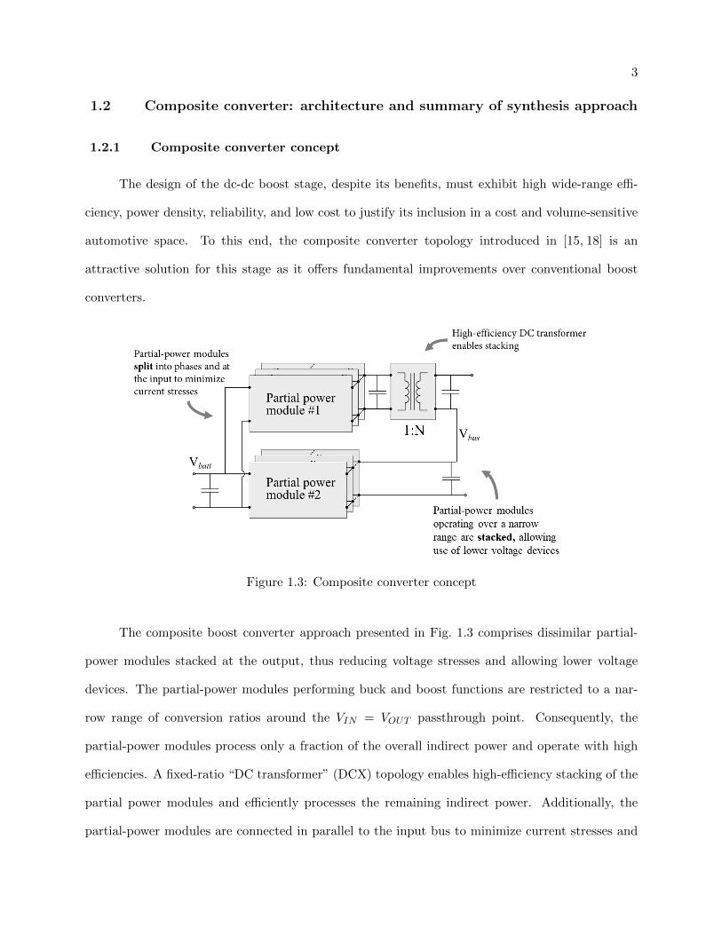
1.2 Composite converter: architecture and summary of synthesis approach
1.2.1 Composite converter concept
The design of the dc-dc boost stage, despite its benefits, must exhibit high wide-range effi-
ciency, power density, reliability, and low cost to justify its inclusion in a cost and volume-sensitive
automotive space. To this end, the composite converter topology introduced in [15, 18] is an
attractive solution for this stage as it offers fundamental improvements over conventional boost
converters.
Figure 1.3: Composite converter concept
The composite boost converter approach presented in Fig. 1.3 comprises dissimilar partial-
power modules stacked at the output, thus reducing voltage stresses and allowing lower voltage
devices. The partial-power modules performing buck and boost functions are restricted to a nar-
row range of conversion ratios around the VIN = VOUT passthrough point. Consequently, the
partial-power modules process only a fraction of the overall indirect power and operate with high
efficiencies. A fixed-ratio “DC transformer” (DCX) topology enables high-efficiency stacking of the
partial power modules and efficiently processes the remaining indirect power. Additionally, the
partial-power modules are connected in parallel to the input bus to minimize current stresses and

4
may further employ multiple interleaved phases to reduce system capacitor requirements.
Figure 1.4: (a) Sic-based 30 kW, 800 V composite converter topology, and (b) Performance im-provement of the composite architecture over conventional boost converter [47]
A 30 kW SiC composite converter capable of boosting up to 800 V output voltage was demon-
strated in [47]. Figure 1.4(a) illustrates the topology consisting of a 2-phase boost converter on
the bottom leg, a 2-phase buck, and a 1:1.5 turns-ratio dual active bridge on the top leg. The per-
formance improvement of this topology over conventional boost converter is plotted in Fig. 1.4(b).
The composite converter efficiency peaks at lower power operating points and remains fairly flat,
maximizing drive-cycle averaged efficiencies.
1.2.2 Summary of the composite-converter synthesis approach
The synthesis of composite converter architectures is quite involved. A scalable approach to
synthesis and optimal design of composite converter architecture given a set of system specifications
and design constraints is presented in [34]. A brief overview of this approach is presented here.
Synthesis of composite converter architecture exhibiting an EV drive-cycle tailored efficiency
characteristic, from the generalized two-leg composite topology shown in Fig. 1.5 for the system
specifications and design constraints in Table 1.1 requires two main steps -
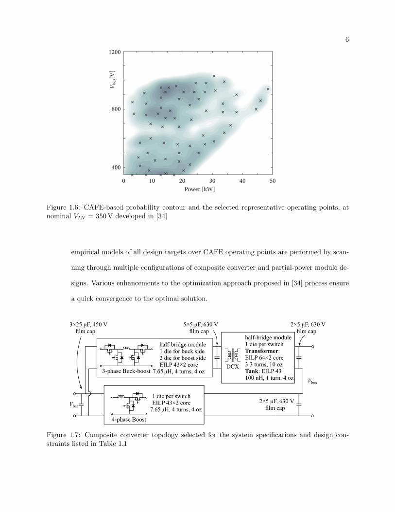
(1) Generation of CAFE-based subset of operating points for the dc-dc stage: The
city and highway drive-cycle operating points for the dc-dc boost stage —extracted from
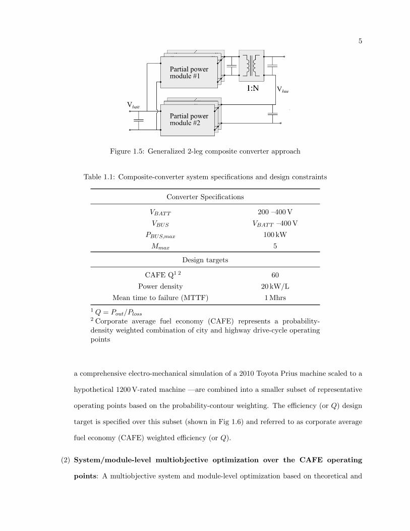
5
Figure 1.5: Generalized 2-leg composite converter approach
Table 1.1: Composite-converter system specifications and design constraints
Converter Specifications
VBATT 200 –400 V
VBUS VBATT –400 V
PBUS,max 100 kW
Mmax 5
Design targets
CAFE Q1 2 60
Power density 20 kW/L
Mean time to failure (MTTF) 1 Mhrs
1 Q = Pout/Ploss2 Corporate average fuel economy (CAFE) represents a probability-density weighted combination of city and highway drive-cycle operatingpoints
a comprehensive electro-mechanical simulation of a 2010 Toyota Prius machine scaled to a
hypothetical 1200 V-rated machine —are combined into a smaller subset of representative
operating points based on the probability-contour weighting. The efficiency (or Q) design
target is specified over this subset (shown in Fig 1.6) and referred to as corporate average
fuel economy (CAFE) weighted efficiency (or Q).
(2) System/module-level multiobjective optimization over the CAFE operating
points: A multiobjective system and module-level optimization based on theoretical and
6
Figure 1.6: CAFE-based probability contour and the selected representative operating points, atnominal VIN = 350 V developed in [34]
empirical models of all design targets over CAFE operating points are performed by scan-
ning through multiple configurations of composite converter and partial-power module de-
signs. Various enhancements to the optimization approach proposed in [34] process ensure
a quick convergence to the optimal solution.
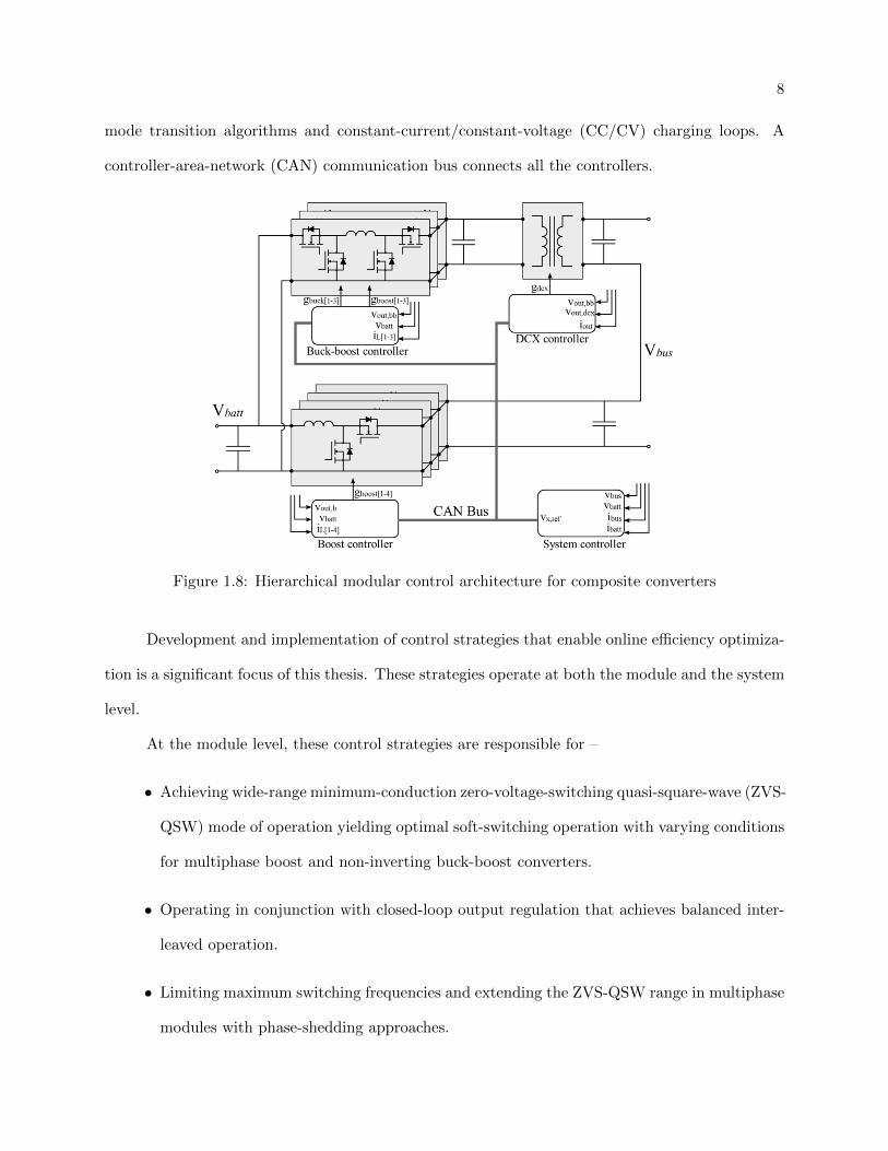
Figure 1.7: Composite converter topology selected for the system specifications and design con-straints listed in Table 1.1

7
The outcome of this synthesis approach is the fully specified composite converter topology
shown in Fig. 1.7 with the following salient features:
• A four-phase boost on the bottom leg and a three-phase non-inverting buck-boost on the
top leg followed by 1 : 1 effective turns-ratio dual active bridge (DAB) based DCX.
• The partial-power modules employ die-configurable half-bridge SiC modules provided by
Wolfspeed. Driven by trade-offs between reliability and efficiency, the non-inverting buck-
boost utilizes an asymmetric die configuration with 1-die devices for the buck bridge and
2-die devices for the boost bridge.
• All magnetic components are realized through planar technology. All inductors are rated
for a 90 A peak current.
As reported in Table 1.2, the modeled performance of the converter beats the design targets
by wide margins.
Table 1.2: Comparison of composite converter design constraints vs modeled performance
Parameter Design targets Modeled performance
CAFE-Q 60 98.9
Power density 20 kW/L 23.5 kW/L
MTTF 1 Mhrs 1.9 Mhrs
1.3 Control system architecture for composite converters
Given the composite converter topology in Fig. 1.7, this work begins with the specification of
a control system architecture and the primary control objectives. Figure 1.8 depicts a hierarchical
modular control architecture for the composite converter topology that consists of module-level and
system-level controllers. The module-level controllers are responsible for high-bandwidth output
regulation, transient response behaviors, and module-level protections for the corresponding partial-
power module. System-level controls include low-bandwidth tasks such as composite converter
8
mode transition algorithms and constant-current/constant-voltage (CC/CV) charging loops. A
controller-area-network (CAN) communication bus connects all the controllers.
Figure 1.8: Hierarchical modular control architecture for composite converters
Development and implementation of control strategies that enable online efficiency optimiza-
tion is a significant focus of this thesis. These strategies operate at both the module and the system
level.
At the module level, these control strategies are responsible for –
• Achieving wide-range minimum-conduction zero-voltage-switching quasi-square-wave (ZVS-
QSW) mode of operation yielding optimal soft-switching operation with varying conditions
for multiphase boost and non-inverting buck-boost converters.
• Operating in conjunction with closed-loop output regulation that achieves balanced inter-
leaved operation.
• Limiting maximum switching frequencies and extending the ZVS-QSW range in multiphase
modules with phase-shedding approaches.

9
Composite converter relies on efficient operating modes that specify what fraction of the
overall output voltage each partial-power module must contribute for a given input to output voltage
conversion ratio. The system-level controller determines the optimal partial-power operating modes
and achieves mode transitions that maximize efficiencies for a given conversion ratio. Additionally,
it must incorporate module-level efficiency optimization strategies.
The subsequent chapters of this thesis are organized as follows:
• Chapter 2 develops an online efficiency-optimization strategy for a half-bridge boost mod-
ule with bidirectional power flow with extensive validation of the proposed optimization
strategy on a single-phase boost converter prototype.
• Chapter 3 presents various considerations for extending these strategies to the multi-
phase boost and non-inverting buck-boost modules. Additionally, a frequency-based phase-
shedding technique that limits maximum converter frequencies and expands the ZVS-QSW
range is introduced.
• Chapter 4 addresses system-level control considerations and describes the composite con-
verter modes that maximize efficiency for a given operating point. Characterization of
composite converter efficiencies is presented combining module and system-level efficiency-
optimization control strategies.
• Chapter 5 concludes the thesis and presents directions for future research and development.

Chapter 2
Efficiency-optimized Control for a Half-bridge Boost Module
Frequency-dependent switching losses present a significant impediment to realizing high-
frequency compact switched-mode power converters [48]. Of principal concern are the turn-on
switching losses primarily dependent on the device parasitic output capacitances and the reverse
recovery of the rectifier body diodes. Particularly with fast turn-off wide band-gap devices, the
turn-on losses tend to be the dominant loss mechanism in high-frequency hard-switched converters
[4,9,43,53]. Reducing the turn-on losses is the key to achieving higher efficiencies, especially for wide
operating range converters such as PFC-rectifiers [40,61,71,76], inverters [39,63], and bidirectional
dc-dc converters in electric-vehicle (EV) powertrain applications [15,21,32,68].
This chapter develops an online efficiency optimization strategy for a half-bridge boost module
that achieves a significant reduction in turn-on switching losses by employing a well-known optimal
soft-switching technique called minimum-conduction zero-voltage-switched quasi square-wave mode
of operation. This optimization strategy, operating in conjunction with the feedback regulation of
the output voltage feedback, precisely adjusts the converter switching frequency and dead times
to ensure minimum-conduction ZVS-QSW operation with varying input/output voltages and bidi-
rectional power flow. In Sect.2.1, a qualitative introduction to turn-on switching loss is presented
by inspecting the main-switch turn-on transition of a boost converter switching cell. Various loss
components of this transition are diagrammed and the zero-voltage-switching quasi-square-wave
mode of converter operation that results in a significant reduction of these losses is discussed. This
soft-switching technique can be further optimized to yield the minimum-conduction ZVS-QSW

11
operation. The converter operation is these modes are visualized through normalized state-plane
representations. Section 2.2 provides a broad overview of the proposed online-optimization control
scheme that maintains minimum-conduction ZVS-QSW operation through optimal adjustment of
converter timing parameters at a given operating point. Section 2.3 illustrates the variation in op-
timal timing parameters with operating conditions and develops comprehensive analytical models
that capture this variation across the converter’s entire operating range. In Sect. 2.4, multivariate
polynomial curve-fitting approaches are developed for these analytical models, and implementation
details are discussed. Experimental results in Section 2.5 validate the proposed online-optimization
approach for bidirectional power flow as well as in transient operation. Additionally, efficiencies
achieved under varying operating conditions with this strategy are compared with conventional
fixed frequency/dead-time operation and single-parameter optimization approaches. This section
also experimentally illustrates the operational limits within which the converter achieves minimum-
conduction ZVS-QSW operation. These limits imposed on the converter due to various hardware
constraints cause the converter to lose minimum-conduction ZVS-QSW operation outside these
limits resulting in either a suboptimal ZVS or a hard-switched operation.
2.1 Qualitative introduction to turn-on switching losses and minimum-
conduction ZVS-QSW operation
A boost converter switching cell depicted in Fig.2.1(a) comprises a main switch Q1 and the
rectifier switch Q2 connected to an inductor L. The input and output voltages on the cell are VIN
and VOUT , respectively, and a current iL flows into the switch-node through the inductor. The
parasitic output capacitances of the two devices are lumped into a single half-bridge equivalent
capacitance, Ceq,Q. The theoretical waveforms for the rectifier-switch Q2 turn-off to the main-
switch Q1 turn-on transition are sketched in Fig. 2.1.
At the instant of Q2 turn-off, iL switches from the channel to the body diode of the switch
Q2. Once the dead-time period elapses, the main switch Q1 turns on, and the inductor current now
shifts to the Q1 channel. The Q1 channel, in addition to the inductor current, must also carry the

12
Figure 2.1: (a) A boost converter switching cell with the device parasitic capacitances lumped intoa single equivalent switch-node capacitance Ceq,Q (b) Hard-switched turn-on transition of the mainswitch Q1.
current resulting from the discharge of the switch-node capacitance and the Q2 body-diode reverse
recovery charge. Therefore, the turn-on loss energy Eon is the sum of the three components as
shown in Eqn. (2.1).
Eon =
∫onichvDSdt = Eoverlap + Eoss + Err (2.1)
where Eoverlap is the energy lost due to the overlap of the inductor current and drain-source voltage
across Q1, Eoss is the energy stored in the switch-node capacitance, and Err is the energy associated
with the losses due to reverse recovery process of the Q2 body diode [29]. The Eoverlap losses for a
given inductor current are proportional to the voltage that Q1 blocks when it turns on, whereas the
Eoss loss is proportional to the square of this voltage. In a boost converter each switch blocks the
output voltage VOUT if the off state. Given the hard-switched operation indicated in the waveforms
of Fig. 2.1(b), the overlap and Eoss losses are proportional to VOUT and V 2OUT respectively. This
dependence of these two turn-on loss mechanisms on the output voltage imposes a severe penalty on
system CAFE-Q in an electric vehicle application due to the prevalence of high-voltage, low-current
operating points in a typical drive cycle [16,33]. A detailed treatment of switching loss mechanisms
13
is provided in [9, 29,53].
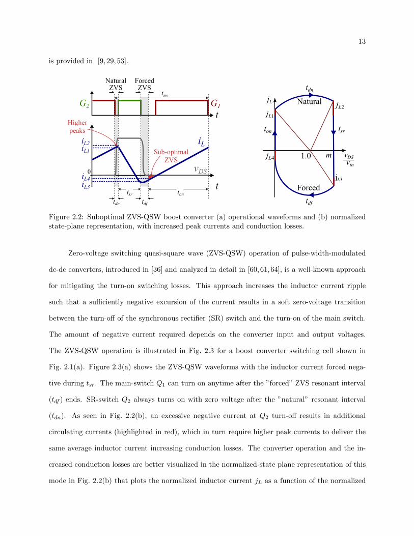
Figure 2.2: Suboptimal ZVS-QSW boost converter (a) operational waveforms and (b) normalizedstate-plane representation, with increased peak currents and conduction losses.
Zero-voltage switching quasi-square wave (ZVS-QSW) operation of pulse-width-modulated
dc-dc converters, introduced in [36] and analyzed in detail in [60,61,64], is a well-known approach
for mitigating the turn-on switching losses. This approach increases the inductor current ripple
such that a sufficiently negative excursion of the current results in a soft zero-voltage transition
between the turn-off of the synchronous rectifier (SR) switch and the turn-on of the main switch.
The amount of negative current required depends on the converter input and output voltages.
The ZVS-QSW operation is illustrated in Fig. 2.3 for a boost converter switching cell shown in
Fig. 2.1(a). Figure 2.3(a) shows the ZVS-QSW waveforms with the inductor current forced nega-
tive during tsr. The main-switch Q1 can turn on anytime after the ”forced” ZVS resonant interval
(tdf ) ends. SR-switch Q2 always turns on with zero voltage after the ”natural” resonant interval
(tdn). As seen in Fig. 2.2(b), an excessive negative current at Q2 turn-off results in additional
circulating currents (highlighted in red), which in turn require higher peak currents to deliver the
same average inductor current increasing conduction losses. The converter operation and the in-
creased conduction losses are better visualized in the normalized-state plane representation of this
mode in Fig. 2.2(b) that plots the normalized inductor current jL as a function of the normalized
14
switch-node voltage. The current normalization factor iB is defined as vIN/R0 where R0 is the
characteristic impedance√L/Ceq,Q. These losses can be minimized by optimally setting the neg-
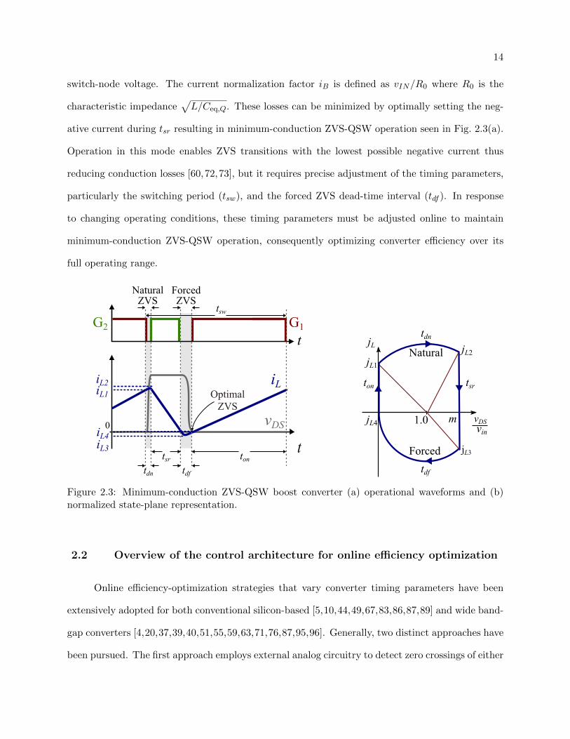
ative current during tsr resulting in minimum-conduction ZVS-QSW operation seen in Fig. 2.3(a).
Operation in this mode enables ZVS transitions with the lowest possible negative current thus
reducing conduction losses [60,72,73], but it requires precise adjustment of the timing parameters,
particularly the switching period (tsw), and the forced ZVS dead-time interval (tdf ). In response
to changing operating conditions, these timing parameters must be adjusted online to maintain
minimum-conduction ZVS-QSW operation, consequently optimizing converter efficiency over its
full operating range.
Figure 2.3: Minimum-conduction ZVS-QSW boost converter (a) operational waveforms and (b)normalized state-plane representation.
2.2 Overview of the control architecture for online efficiency optimization
Online efficiency-optimization strategies that vary converter timing parameters have been
extensively adopted for both conventional silicon-based [5,10,44,49,67,83,86,87,89] and wide band-
gap converters [4,20,37,39,40,51,55,59,63,71,76,87,95,96]. Generally, two distinct approaches have
been pursued. The first approach employs external analog circuitry to detect zero crossings of either
15
inductor current (ZCD) [40, 67, 71, 76, 83, 95] or switch-node voltage (ZVD) [37, 87, 96] and adjusts
timing parameters based on this information. This approach typically leads to implementation
complexity with sensitivity to noise and delays. Moreover, it also suffers from a lack of flexibility
since most converters considered have only unidirectional power flow. Reference [76] demonstrates
optimization for both inductor current polarities with two comparator circuits and flipping the
edge-trigger logic based on polarity.
The second class of online optimization approaches relies entirely on digital implementation.
For example, in [5, 89] the converter timing parameters are perturbed over a range and values
that maximize efficiency are applied. This strategy requires long convergence times for wide op-
erating ranges and may not achieve maximal efficiency since only one of the timing parameters is
swept. Lookup table-based approaches that adjust switching frequencies and operational modes
based on theoretical or empirically-determined table entries for a given operating condition are
adopted in [44, 63]. In applications where both the input/output voltages and converter power
levels must vary, the table dimensions grow, increasing storage requirements and complexity. Ap-
proaches that directly compute the timing parameters are presented in [4, 10, 39, 49, 55, 59]. These
approaches reduce the computational complexity by fixing one parameter such as peak SR turn-off
current [10, 39, 49], dead times [4, 55], or frequency [59] and online-adjusting the remaining pa-
rameter. This results in either hard-switched or sub-optimal ZVS operation over specific ranges.
A hybrid modulation strategy combining the discontinuous conduction and ZVS-QSW mode by
introducing additional switching intervals is proposed in [51]. Generally speaking, few previously
presented approaches achieve minimum-conduction ZVS-QSW operation over wide ranges since
most of them can vary only a single timing parameter. While it may theoretically be possible
to extend some of these approaches to both frequency and dead times, the resulting increase in
complexity could end up being prohibitive in practical implementation. The only exception is [86]
which demonstrates a control strategy that modifies both switching frequency and forced ZVS dead
times, and demonstrates bidirectional power flow for a conventional silicon-based boost converter.
However, this work oversimplifies the calculation of timing parameters by approximating the reso-
16
nant dead-time intervals as linear regions, and fails to capture the impact of varying switch-node
capacitance.
The optimization strategy proposed in this chapter achieves wide-range minimum-conduction
ZVS-QSW operation by online adjusting both the converter switching frequency and the forced-
ZVS dead time. The direct computation of the optimal timing parameters is achieved through
multivariate polynomial functions that are developed offline from surface-fitting the analytical so-
lutions and are easily implemented in the controller. A low-bandwidth feed-forward loop operating
concurrently with the feedback loop evaluates the polynomial functions that generate the optimal
timing parameters for sensed input/output voltages and average inductor current.
Calculation of the optimal switching frequency and dead times requires a solution of the
minimum-conduction ZVS-QSW state plane representation shown in Fig. 2.3(b). Although the
timing parameters calculated from the minimum-conduction ZVS-QSW state plane are unique
for a given combination of input voltage vIN , conversion ratio m, and processed power (average
inductor current), the state-plane equations governing the converter’s operation in this mode do
not have straightforward closed-form expressions. They must be numerically solved to obtain the
timing parameters. Since such a numerical computation is not suitable for direct implementation
on a controller platform, a twofold approach to simplifying online optimization is adopted in this
work. As a first step, analytical models for optimal timing parameters, fsw and tdf , are developed
offline through numerical solution of the minimum-conduction ZVS-QSW state-plane for the entire
region of converter operation. A multivariate polynomial function is then fit to these theoretical
models using a standard curve fitting toolbox [62]. This approach, first introduced in [74], simplifies
the online-optimization to evaluating polynomial functions (fit functions) that yield the optimal
timing parameters for given operating conditions. The fit functions are then easily implemented
on a microcontroller platform and evaluated in a low-bandwidth feed-forward loop operating in
conjunction with the feedback loop.
Figure 2.4 presents the resulting control architecture. The feedback loop responsible for the
output voltage regulation contains an outer voltage loop followed by an inner average current-
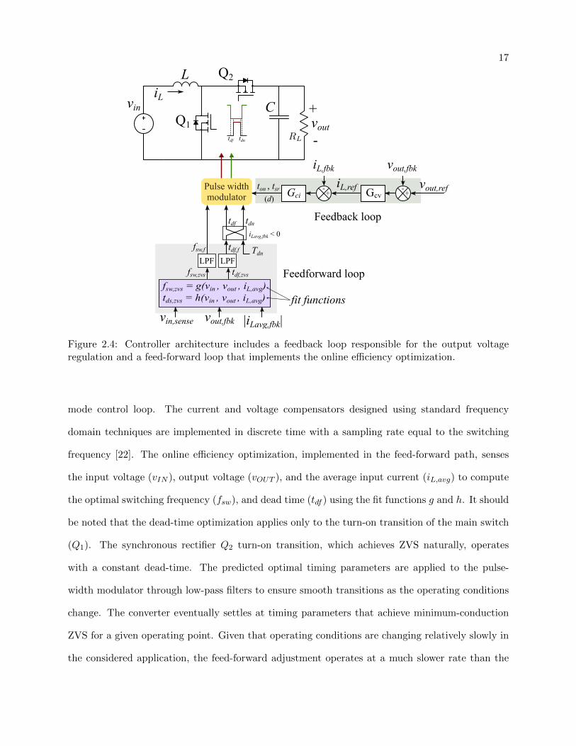
17
Figure 2.4: Controller architecture includes a feedback loop responsible for the output voltageregulation and a feed-forward loop that implements the online efficiency optimization.
mode control loop. The current and voltage compensators designed using standard frequency
domain techniques are implemented in discrete time with a sampling rate equal to the switching
frequency [22]. The online efficiency optimization, implemented in the feed-forward path, senses
the input voltage (vIN ), output voltage (vOUT ), and the average input current (iL,avg) to compute
the optimal switching frequency (fsw), and dead time (tdf ) using the fit functions g and h. It should
be noted that the dead-time optimization applies only to the turn-on transition of the main switch
(Q1). The synchronous rectifier Q2 turn-on transition, which achieves ZVS naturally, operates
with a constant dead-time. The predicted optimal timing parameters are applied to the pulse-
width modulator through low-pass filters to ensure smooth transitions as the operating conditions
change. The converter eventually settles at timing parameters that achieve minimum-conduction
ZVS for a given operating point. Given that operating conditions are changing relatively slowly in
the considered application, the feed-forward adjustment operates at a much slower rate than the

18
voltage regulation loop. Furthermore, as discussed further in Section 2.4.2, the proposed online-
optimization strategy is easily extended to bidirectional power flow by utilizing the absolute value
of the sensed average inductor current.
2.3 Timing parameters for minimum-conduction ZVS-QSW operation
A systematic approach to numerically solving a boost converter minimum-conduction state
plane for the optimal timing parameters over the full operating range is shown in Appendix A.
Before developing the analytical models and the resulting fit-functions from the solutions, it is
helpful to inspect the trajectory of the optimal timing parameters for variation in each of the
converter operating conditions (m, iL,avg, vIN ). This step yields insight into the converter operation
in minimum-conduction ZVS-QSW mode as well as the curve-fitting process.
2.3.1 Variation with conversion ratio m
Figure 2.5 shows the optimal switching frequency (fsw) and forced ZVS dead time (tdf ) as
functions of the conversion ratio m defined as m = vOUT /vIN . The plot is generated from the
analytical solutions by fixing the converter output voltage at 500 V (thereby fixing the equivalent
switch-node capacitance) and the average inductor current at 25 A, and by varying the input voltage
from 200 V to 400 V to vary m from 1.25 to 2.5. The optimal fsw shows a parabolic dependence
on m, with maxima at m = 2, whereas the optimal tdf splits into two curves across the m = 2
conversion line. The converter operation in minimum-conduction ZVS-QSW mode can be divided
into two distinct regions of operation, as illustrated in the state-plane diagrams of Fig. 2.6.
The m < 2 continuous conduction-mode of Fig. 2.6(a) requires a negative-current jL3 at the
synchronous-rectifier Q2 turn-off instant to satisfy the forced ZVS condition j2L3 + (m − 1)2 ≥ 1.
Setting the two terms equal results in minimum-conduction ZVS operation with jL3 set optimally
and the main switch Q1 turning on at strictly zero current and zero voltage.
Increasing m shifts the point (1.0, 0) on the state-plane horizontal axis inward towards (0, 0).
The optimal jL3 decreases (less-negative), resulting in smaller rectifier turn-on time tsr, thereby

19
Figure 2.5: Optimal fsw and tdf as functions of the conversion ratio m for fixed vOUT = 500 V andiL,avg = 25 A, and vIN varying from 200 V to 400 V.
Figure 2.6: State-plane diagrams for converter operation in (a) m < 2 continuous-conduction modeand (b) m > 2 boundary conduction mode.
increasing fsw. The normalized angle β becomes larger, increasing tdf . At m = 2, the point where
1 and m− 1 segments on the state plane are equal, both Q2 turn-off and Q1 turn-on occur at zero
current with optimal fsw and tdf reaching their maximum values. Angle β traverses an angle of π
with tdf = π√LCoss,Q. Increasing m further results in m > 2 boundary conduction mode shown in
Fig. 2.6(b). Turning off Q2 at strictly zero current results in minimum-conduction ZVS with Q1 now
turning on with optimal negative current jL4. Optimal jL4 follows the equation j2L4 + 1 = (m−1)2.
Both the optimal fsw and tdf decrease with increasing m in the boundary conduction mode. Even
though a negative current is not required in the boundary conduction mode since the converter

20
”naturally” achieves ZVS turn-on for Q1, precise timing parameter adjustments are still required
to ensure the rectifier switch turn off at zero current (to avoid body-diode conduction) in order to
achieve the minimum-conduction ZVS-QSW operation.
The optimal timing parameters are strongly dependent on the conversion ratio m. A curve-
fitting approach for optimal fsw requires a higher-order fit with respect to m. Optimal tdf requires
two independent fits across the m = 2 conversion boundary.
2.3.2 Variation with conversion ratio iL,avg
Figure 2.7(a) plots the optimal switching period and forced dead-time interval as functions of
the average inductor current (iL,avg) from 5-50 A with vIN fixed at 300 V and 500 V, respectively.
As evident from the state-plane diagram of Fig. 2.7(b), the jL < 0 region (negative vertical axis) is
independent of iL,avg, implying that the Q2 turn-off and Q1 turn-on currents (jL3 and jL4), and the
forced ZVS interval tdf depend only on the input and output voltages of the converter. Optimal tdf ,
therefore, remains constant for a given vIN and vOUT , whereas optimal tsw linearly increases with
iL,avg to accommodate the increasing values of ton and tsr, thereby implying an inverse dependence
of the optimal fsw on iL,avg.
Figure 2.7: (a) Optimal switching period, tsw, and forced dead-time interval, tdf as functions ofiL,avg varying from 5 A to 50 A for fixed vIN = 300 V and vOUT = 500 V, and (b) state-planediagrams for two different average inductor currents.

21
2.3.3 Effect of varying switch-node capacitance
The device parasitic output capacitance Coss exhibits a highly non-linear drain-source voltage
dependence. An analytical approach for taking the equivalent half-bridge switch-node capacitance
Ceq,Q (of Fig. 2.1(a)) into account is described in [24, 45] and requires calculating the charge-
equivalent capacitance Ceq,Q as per (2.2).
Ceq,Q =1
Vout
∫ Vout
0(Coss(v) + Coss(Vout − v)) dv (2.2)
Figure 2.8: (a) Measurement-based calibration of the equivalent switch-node capacitance calculatedfrom the oscillation period of the switch-node voltage in m = 2 discontinuous mode of operation,and (b) Charge-equivalent switch-node capacitance Ceq,Q of the half-bridge module as a functionof the dc output voltage using both analytical and the indirect measurement-based method.
Alternatively, an indirect measurement-based method can also be employed to accurately
estimate the equivalent switch-node capacitance for a given output voltage. In this approach, the
converter is purposely operated in discontinuous conduction mode (DCM) at a conversion ratio
of m = 2 for a specific input voltage, as illustrated in the waveforms of Fig 2.8(a). Once the
inductor current drops to zero at the end of the rectifier-diode turn-on interval, it continues to ring
with Ceq,Q. The switch-node voltage oscillates around Vin and, given a conversion ratio of exactly
2, attain a peak amplitude of 2Vin traversing switch-node voltage from 0 to Vout. The effective
capacitance Ceq,Q at Vout can be calculated from the observed oscillation period with a known
inductance L and is given as Ceq,Q = 1/(2πtprdL2). Consequently, by varying the input voltage
and adjusting the Q1 and Q2 turn-on intervals to ensure m = 2 DCM operation, Ceq,Q can be
22
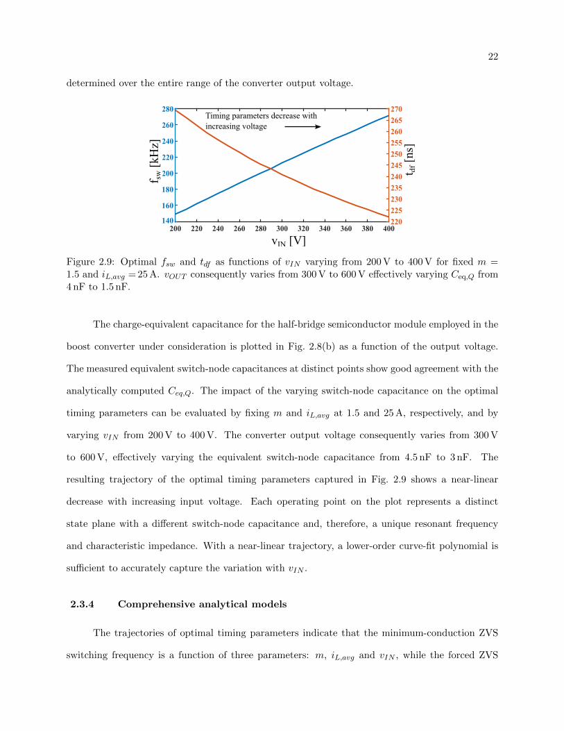
determined over the entire range of the converter output voltage.
Figure 2.9: Optimal fsw and tdf as functions of vIN varying from 200 V to 400 V for fixed m =1.5 and iL,avg = 25 A. vOUT consequently varies from 300 V to 600 V effectively varying Ceq,Q from4 nF to 1.5 nF.
The charge-equivalent capacitance for the half-bridge semiconductor module employed in the
boost converter under consideration is plotted in Fig. 2.8(b) as a function of the output voltage.
The measured equivalent switch-node capacitances at distinct points show good agreement with the
analytically computed Ceq,Q. The impact of the varying switch-node capacitance on the optimal
timing parameters can be evaluated by fixing m and iL,avg at 1.5 and 25 A, respectively, and by
varying vIN from 200 V to 400 V. The converter output voltage consequently varies from 300 V
to 600 V, effectively varying the equivalent switch-node capacitance from 4.5 nF to 3 nF. The
resulting trajectory of the optimal timing parameters captured in Fig. 2.9 shows a near-linear
decrease with increasing input voltage. Each operating point on the plot represents a distinct
state plane with a different switch-node capacitance and, therefore, a unique resonant frequency
and characteristic impedance. With a near-linear trajectory, a lower-order curve-fit polynomial is
sufficient to accurately capture the variation with vIN .
2.3.4 Comprehensive analytical models
The trajectories of optimal timing parameters indicate that the minimum-conduction ZVS
switching frequency is a function of three parameters: m, iL,avg and vIN , while the forced ZVS

23
dead-time interval depends only on m and vIN . The switching frequency analytical model can be
constructed from multiple surfaces wherein each surface represents the optimal fsw for the variation
in vIN and m for a given iL,avg. Analytical model for the optimal tdf consists of two surfaces split
across the m = 2 conversion ratio plane. The comprehensive analytical models for optimal timing
parameters over the converter’s full operating range are developed in Fig. 2.10.
Figure 2.10: Minimum-conduction ZVS-QSW (a) optimal fsw for different iL,avg values, and (b)optimal tdf , both plotted as functions of vIN and m for 2-die half-bridge 7.65 µH boost converterconfiguration.
Each unique combination of a device configuration and an inductor value results in a distinct
set of frequency and dead-time analytical models. The composite converter configuration of this
work requires three different models, as listed in Table 2.1. Due to different device configurations

24
Table 2.1: List of half-bridge analytical models in the benchtop composite system
Module Half-bridge, inductor configuration
4-phase Boost 1-die with 7.65 µH
3-phase Buck-Boost (Boost) 2-die with7.5 µH
3-phase Buck-Boost (Buck) 1-die with 7.5 µH
for the buck and the boost bridges, the buck/boost converter must employ two independent sets
of analytical models. The analytical models of Fig. 2.10 correspond to device configuration and
inductor value for the boost converter. The buck-boost converter analytical models are presented in
Appendix A which also details the steps involved in developing and plotting the models. Input volt-
age vIN is varied from 200 V to 400 V and vOUT from vIN to 600 V, both in steps of 5 V, representing
a theoretical variation of 1.0 to 3.0 in the converter’s conversion ratio m. The average inductor
iL,avg across the optimal fsw surfaces varies from 5 A to 50 A in steps of 5 A. The analytical models
account for the varying Ceq,Q and follow the optimal timing parameter trends presented earlier.
Although the frequency models indicate a wide variation in optimal fsw (from less than 100 kHz to
800 kHz), not all switching frequency values are attainable in the hardware implementation. The
converter is constrained to operate within the limits, fsw,min and fsw,max. Gate-driver ratings set
the maximum switching frequency threshold fsw,max while peak currents on the magnetics set the
lower limit fsw,min. Within these limits, the converter achieves minimum-conduction ZVS-QSW at
all operating points. At operating points that require optimal fsw beyond fsw,max, the converter
operates with sub-optimal ZVS switching frequency clamped to fmax. Likewise, the converter hard
switches with fsw fixed to fsw,min at operating points requiring optimal frequencies below fsw,min.
2.4 Online efficiency optimization using multivariate polynomial curve-
fitting
This section addresses implementation issues related to the online efficiency optimization
strategy where the converter switching frequency and the forced-ZVS dead time are adjusted in re-

25
sponse to operating conditions. Computation of the optimal timing parameters is achieved through
multivariate polynomial functions that are developed from surface-fitting the analytical solutions
developed in Section 2.3.4.
2.4.1 Multivariate polynomial curve-fitting
Based on the dependencies observed in Section 2.3.4, the analytical-model surfaces employ a
poly25 polynomial fit with a second-degree polynomial in input voltage vIN and a fifth-degree in
conversion ratio m. The poly25 polynomial comprises fifteen coefficients and is given by
y(vin,m) = p00 + p10.vin + p01.m+ p20.v2in + p11.vin.m+ p02.m
2
+ p21.v2in.m+ p12.vin.m
2 + p03.m3 + p22.v
2in.m
2 + p13.vin.m3
+ p04.m4 + p23.v
2in.m
3 + p14.vin.m4 + p05.m
5
(2.3)
where y is the optimal timing parameter (fsw or tdf ), and pi,j are the curve-fit coefficients.
The multivariate polynomial fitting of the optimal fsw demonstrated in Fig. 2.11 involves
two steps. First, independent poly25 surfaces corresponding to distinct iL,avg values uniquely fit
each analytical surface from the model. This step results in ten different poly25 surfaces,
fsw∣∣IL,avg=Ik
= p00∣∣Ik
+ p10∣∣Ik.vin + · · ·+ p05
∣∣Ik.m5
(k = 1, 2, · · · , 10)
(2.4)
Figure 2.11(a) illustrates this step for a single optimal fsw surface with iL,avg = 5 A. To
keep the poly25 terms tractable, the vIN axis is normalized with respect to the voltage sensor
full-scale value before the fitting process. In the second step, the corresponding coefficients (e.g.,
p00∣∣I1, p00
∣∣I2· · · p00
∣∣I10
) across the ten poly25 functions are curve-fit with iL,avg. Due to an inverse
dependence of the optimal fsw on the average inductor current, curve fitting the poly25 coefficients
with i−1L,avg results in a better fit. A common curve-fit order is employed across all coefficients
to simplify implementation while adequately reducing the root mean square error (RMSE) for fit
coefficients. Figure 2.11(a) illustrates the fit along with computed RMSE for two coefficients, p10,
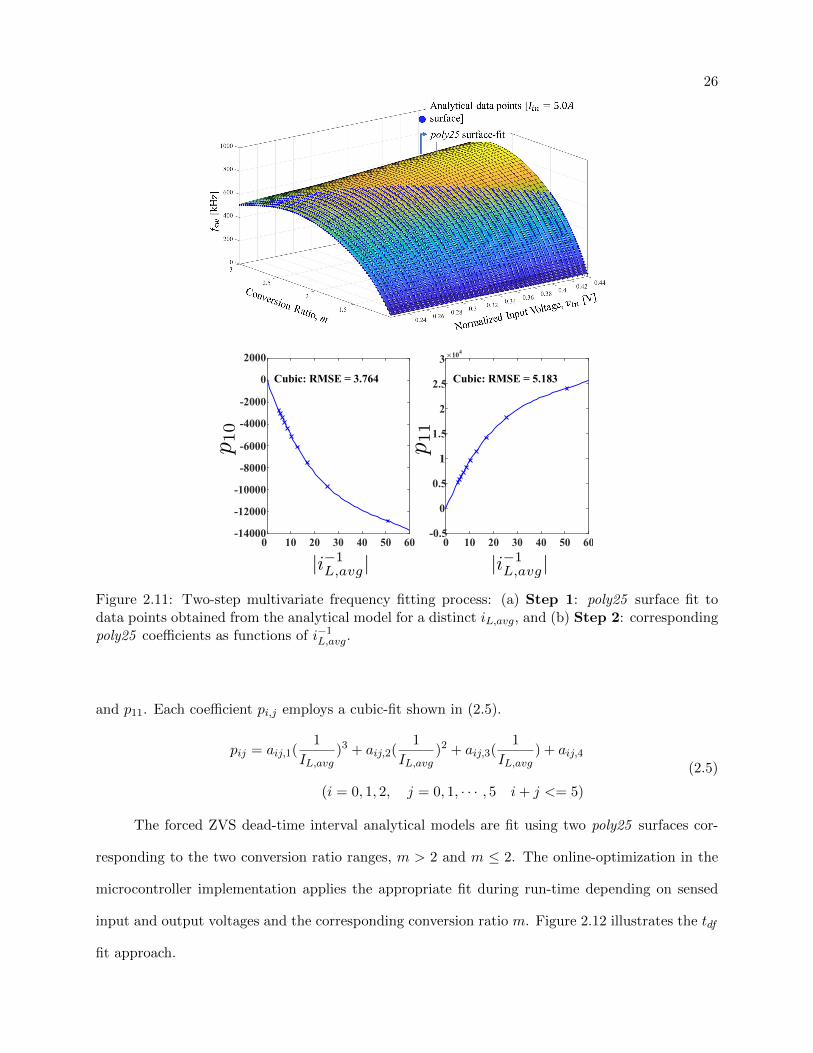
26
Figure 2.11: Two-step multivariate frequency fitting process: (a) Step 1: poly25 surface fit todata points obtained from the analytical model for a distinct iL,avg, and (b) Step 2: correspondingpoly25 coefficients as functions of i−1
L,avg.
and p11. Each coefficient pi,j employs a cubic-fit shown in (2.5).
pij = aij,1(1
IL,avg)3 + aij,2(
1
IL,avg)2 + aij,3(
1
IL,avg) + aij,4
(i = 0, 1, 2, j = 0, 1, · · · , 5 i+ j <= 5)
(2.5)
The forced ZVS dead-time interval analytical models are fit using two poly25 surfaces cor-
responding to the two conversion ratio ranges, m > 2 and m ≤ 2. The online-optimization in the
microcontroller implementation applies the appropriate fit during run-time depending on sensed
input and output voltages and the corresponding conversion ratio m. Figure 2.12 illustrates the tdf
fit approach.

27
Figure 2.12: Illustration of the forced-ZVS dead-time fitting approach.
2.4.2 Extension to bidirectional power flow
When the power flow reverses, the polarity of the average inductor current flips, and the
converter operates in the buck mode. The converter operating waveforms and the minimum-
conduction ZVS-QSW state plane diagram of Fig. 2.3 are redrawn in Fig. 2.13 for reverse power
flow. The converter processes the same power since the absolute value of iLavg, and the input/output
voltages are equal in both cases. The waveforms indicate that a polarity reversal in the inductor
current also flips the definitions of the main and the synchronous rectifier switch. Flipping the
switch definitions implies that the natural and the forced ZVS transition intervals also flip. For an
average negative polarity, the inductor current must now make a small positive excursion to ensure
ZVS turn-on for the switch Q2. The corresponding state-plane representation for reverse power flow
in Fig. 2.13(b) keeps the definitions of the time intervals and instantaneous current labels consistent
with the forward power flow. The forced ZVS dead-time interval flips to the jL > 0 region of the plot
and must be applied to the top switch Q2. Further inspection of the state plane diagram and the
analytical solution for reverse power flow reveals that the optimal timing parameters are identical
in both cases, given the same vIN , vOUT , and |iL,avg|. The analytical models and the curve-fitting
approaches developed in the previous sections are therefore independent of the current polarity. It

28
may also be observed that since the converter mode of operation is defined based on the magnitude
of the current at the rectifier turn-off instant, the continuous and boundary conduction modes of
operation also flip with the current polarity. Nevertheless, there is no impact on the optimal timing
parameters since the definition of the conversion ratio (vOUT /vIN where vOUT > vIN ) is consistent
in both modes. As indicated in the control architecture of Fig. 2.4, the feed-forward loop operates
with |iL,avg|, generates the optimal timing parameters, and applies tdf appropriately to the switch
undergoing the forced-ZVS transition.
Figure 2.13: Minimum-conduction ZVS-QSW for reverse power-flow: (a) operating waveforms, and(b) normalized state-plane diagram.
2.4.3 Evaluation of the curve-fit approach
Residual plots offer an insightful method to evaluate the fit performance and compare different
fit models. Residuals are the differences between the analytical data and fit data. Figure 2.14(a)
plots the residuals from the poly25 fitting of the analytical fsw surface with iL,avg = 20 A, and
Fig. 2.14(b) plots the dead-time residuals for the m > 2 boundary conduction mode surface.
In both plots, the residuals are scattered around zero without displaying a systematic pattern,
demonstrating that the poly25 model fits the analytical data well. Furthermore, the relatively low
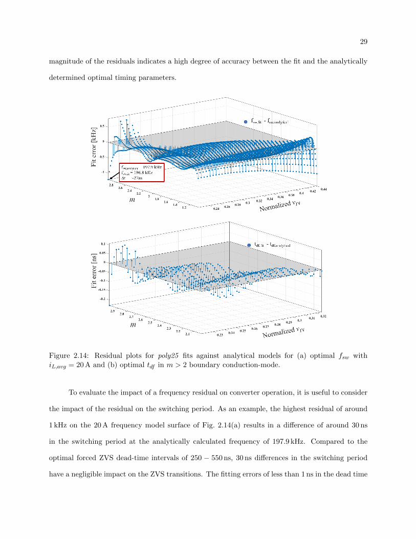
29
magnitude of the residuals indicates a high degree of accuracy between the fit and the analytically
determined optimal timing parameters.
Figure 2.14: Residual plots for poly25 fits against analytical models for (a) optimal fsw withiL,avg = 20 A and (b) optimal tdf in m > 2 boundary conduction-mode.
To evaluate the impact of a frequency residual on converter operation, it is useful to consider
the impact of the residual on the switching period. As an example, the highest residual of around
1 kHz on the 20 A frequency model surface of Fig. 2.14(a) results in a difference of around 30 ns
in the switching period at the analytically calculated frequency of 197.9 kHz. Compared to the
optimal forced ZVS dead-time intervals of 250 − 550 ns, 30 ns differences in the switching period
have a negligible impact on the ZVS transitions. The fitting errors of less than 1 ns in the dead time

30
are smaller than the controller’s minimum adjustable dead time of 2.5 ns. The residuals may also
be converted to fixed percentage errors that are independent of the analytical timing parameters.
The 1 kHz frequency residual, for example, represents an 0.55% error in the switching period.
2.4.4 Current sensing and microcontroller implementation
Figure 2.15: Inductor current sensing for feedback and feed-forward loops
Figure 2.15 illustrates the inductor current sensing strategy. Both the feedback and the feed-
forward loops utilize the output from the common sensing circuit. The sensing circuit consists of an
isolated current-sense amplifier [78] followed by a differential amplifier stage. The isolated amplifier
limits the circuit bandwidth to 950 kHz. Due to the limited bandwidth of the sensing circuit, the
feedback signal is subject to variable operating-point delays, which makes it more challenging to
obtain a precise average value of the sensed inductor current. The low-pass filtered version of
the the sensed signal is therefore provided as a separate input to an independent ADC channel.
The corner frequency of the analog filter is placed at around 1 kHz. This signal is further filtered
digitally to generate a digital representation of the average inductor current, which is then used as
an input to the feed-forward loop, as shown in Fig. 2.4 and Fig. 2.16.
Figure 2.16 shows a flowchart of the microcontroller implementation of the online-optimization
approach. The high-bandwidth feedback loop is executed in an interrupt service routine (ISR) trig-
gered at the controller sampling frequency, which equals the converter switching frequency. The
sampling frequency varies as the converter switching frequency is adjusted. The ISR gets the ADC
results, executes the voltage and the current loop compensator calculations, evaluates the duty
cycle command, and updates the pulse-width modulator (PWM) duty-cycle register based on the

31
Figure 2.16: Controller implementation flowchart.
PWM period register. Additionally, the ISR also applies digital low-pass filters on the sensed ADC
values to provide the feed-forward optimization loop with average values of the sensed converter
signals.
The low-bandwidth feed-forward loop can tolerate a certain amount of jitter between execu-
tion intervals and is therefore implemented outside the interrupt context in the main thread as a
200 Hz scheduled task. The task sequentially performs the frequency and dead-time optimization
steps. Online frequency optimization executes the frequency-fit steps of Section 2.4.1 in reverse.
The controller first computes the fifteen poly25 coefficients from cubic-fit functions of the sensed
average inductor current’s absolute value. Using these coefficients and the sensed input and out-
put voltages, the controller determines the optimal switching frequency by evaluating the poly25
surface-fit equation. The optimal forced ZVS dead time is then calculated by evaluating another
poly25 equation with the appropriate set of coefficients depending on the conversion ratio. The nat-

32
ural ZVS dead time is set to a constant value that ensures safe operation without shoot-through in
all operating conditions. To ensure that the feed-forward timing parameters are modified smoothly
through incremental changes, the optimal timing parameters are applied to the converter through
digital low-pass filters with a conservatively designed corner frequency of approximately 6 Hz to
minimize the impact on the feedback loops, while providing sufficiently fast updates to the timing
parameters in response to changes in operating conditions. The variables for natural and forced
ZVS dead times are updated based on the inductor current polarity. The PWM registers are up-
dated inside the feedback loop interrupt right before the computation of the duty cycle counts to
ensure integrity of the duty cycle with varying switching frequency.
The online-optimization strategy collectively for the two parameters requires storing 90
floating-point coefficients (50 cubic-fit and 30 poly25 coefficients) and computation of 17 curve-fit
equations (15 cubic-fit and two poly25 ) in addition to evaluating exponents of the input parame-
ters. These requirements are relatively small for modern microcontroller architectures [82]. The
overall execution time of 20 µs for the optimization algorithm (with feedback interrupts disabled)
measured on the utilized controller platform is only a small fraction of the period of the 200 Hz
feed-forward loop execution rate. Additionally, a 200 MHz clock of the controller platform (Table
2.2) allows for a 5 ns resolution in period adjustment that is adequate for a 100 kHz to 400 kHz
switching frequency range considered in this application.
2.4.5 Offline validation of the online-optimization strategy
Before implementing the optimization approach on the hardware prototype, an offline vali-
dation of the algorithm is performed by feeding the feed-forward optimization loop with a vector
of arbitrarily generated signals representing input/output voltages and average inductor currents.
The values received by the 200 Hz feed-forward loop are updated every second. The results for fre-
quency and dead-time offline validation are shown in Fig.2.17(a) and (b), respectively. The curve-fit
timing parameters represented by dashed lines closely match the analytical values shown in bold
red. The low-pass filtered values of the timing parameters applied in the converter controller are
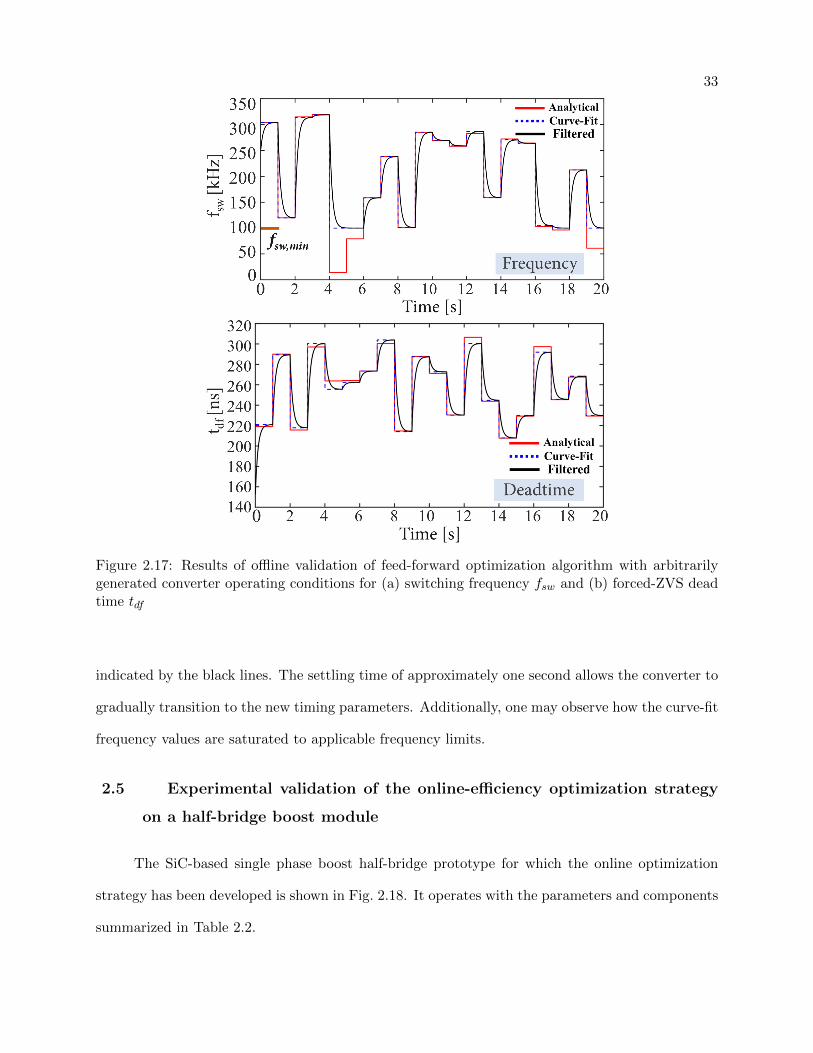
33
Figure 2.17: Results of offline validation of feed-forward optimization algorithm with arbitrarilygenerated converter operating conditions for (a) switching frequency fsw and (b) forced-ZVS deadtime tdf
indicated by the black lines. The settling time of approximately one second allows the converter to
gradually transition to the new timing parameters. Additionally, one may observe how the curve-fit
frequency values are saturated to applicable frequency limits.
2.5 Experimental validation of the online-efficiency optimization strategy
on a half-bridge boost module
The SiC-based single phase boost half-bridge prototype for which the online optimization
strategy has been developed is shown in Fig. 2.18. It operates with the parameters and components
summarized in Table 2.2.
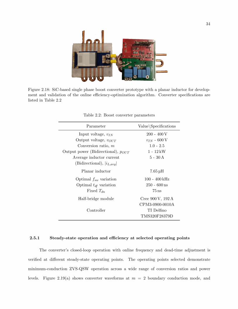
34
Figure 2.18: SiC-based single phase boost converter prototype with a planar inductor for develop-ment and validation of the online efficiency-optimization algorithm. Converter specifications arelisted in Table 2.2
Table 2.2: Boost converter parameters
Parameter Value\Specifications
Input voltage, vIN 200 - 400 V
Output voltage, vOUT vIN - 600 V
Conversion ratio, m 1.0 - 2.5
Output power (Bidirectional), pOUT 1 - 12 kW
Average inductor current 5 - 30 A
(Bidirectional), |iL,avg|
Planar inductor 7.65 µH
Optimal fsw variation 100 - 400 kHz
Optimal tdf variation 250 - 600 ns
Fixed Tdn 75 ns
Half-bridge module Cree 900 V, 192 A
CPM3-0900-0010A
Controller TI Delfino
TMS320F28379D
2.5.1 Steady-state operation and efficiency at selected operating points
The converter’s closed-loop operation with online frequency and dead-time adjustment is
verified at different steady-state operating points. The operating points selected demonstrate
minimum-conduction ZVS-QSW operation across a wide range of conversion ratios and power
levels. Figure 2.19(a) shows converter waveforms at m = 2 boundary conduction mode, and
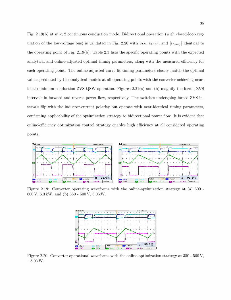
35
Fig. 2.19(b) at m < 2 continuous conduction mode. Bidirectional operation (with closed-loop reg-
ulation of the low-voltage bus) is validated in Fig. 2.20 with vIN , vOUT , and∣∣iL,avg∣∣ identical to
the operating point of Fig. 2.19(b). Table 2.3 lists the specific operating points with the expected
analytical and online-adjusted optimal timing parameters, along with the measured efficiency for
each operating point. The online-adjusted curve-fit timing parameters closely match the optimal
values predicted by the analytical models at all operating points with the converter achieving near-
ideal minimum-conduction ZVS-QSW operation. Figures 2.21(a) and (b) magnify the forced-ZVS
intervals in forward and reverse power flow, respectively. The switches undergoing forced-ZVS in-
tervals flip with the inductor-current polarity but operate with near-identical timing parameters,
confirming applicability of the optimization strategy to bidirectional power flow. It is evident that
online-efficiency optimization control strategy enables high efficiency at all considered operating
points.
Figure 2.19: Converter operating waveforms with the online-optimization strategy at (a) 300 -600 V, 6.3 kW, and (b) 350 - 500 V, 8.0 kW.
Figure 2.20: Converter operational waveforms with the online-optimization strategy at 350 - 500 V,−8.0 kW.

36
Figure 2.21: Magnified forced-ZVS transitions at 350 - 500 V, 8 kW for (a) forward and (b) reversepower flow.
2.5.2 Transient operation with online optimization
Figure 2.22 captures the converter’s closed-loop transient response for a step-change in the
output voltage reference from 400 V to 500 V, with the input voltage fixed at 300 V. This output
voltage step results in a corresponding step in the output power from 3 kW to 7.5 kW. The results
confirm that voltage regulation is unaffected by the feed-forward optimization of timing parameters.
The overshoot of about 25% in the inductor current results in a short settling time of about
a millisecond for the output voltage. Before the transient is applied, the converter operates with
optimal timing parameters of 316.7 kHz and 230 ns with a measured steady-state efficiency of 99.1%.
Post application of the step-reference transient, the converter settles at the new optimal values of
255.3 kHz and 255 ns over around 100 ms time interval to a new steady state with a measured
efficiency of 98.9%. The waveform inserts in Fig. 2.22 that illustrate the steady-state operation
before and after the transient confirm that the converter maintains minimum-conduction ZVS-QSW
operation with changing operating conditions.
Table 2.3: Comparison of analytical and curve-fit optimal frequencies and dead times, togetherwith measured efficiencies at the steady-state operating points of Fig. 2.19 and Fig. 2.20.
Operating Point Analytical values Curve-fit values Conduction MeasuredFig. Vin m IL,avg Fsw Tdr Fsw Tdr Mode Efficiency
2.19(a) 299.1 V 2.0 21.2 A 354.4 kHz 325 ns 353.8 kHz 320 ns boundary 98.6 %2.19(b) 350.2 V 1.4 21.4 A 253.2 kHz 225 ns 253.2 kHz 230 ns continuous 99.2 %
2.20 353.4 V 1.4 −21.3 A 252.8 kHz 225 ns 248.3 kHz 230 ns boundary 99.0 %
37
Figure 2.22: Closed-loop transient response with feed-forward optimization for a voltage referencestep from 400 V to 500 V.
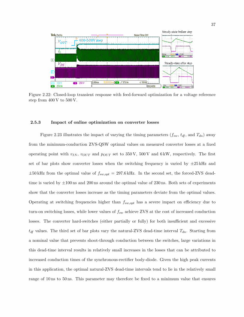
2.5.3 Impact of online optimization on converter losses
Figure 2.23 illustrates the impact of varying the timing parameters (fsw, tdf , and Tdn) away
from the minimum-conduction ZVS-QSW optimal values on measured converter losses at a fixed
operating point with vIN , vOUT and pOUT set to 350 V, 500 V and 6 kW, respectively. The first
set of bar plots show converter losses when the switching frequency is varied by ±25 kHz and
±50 kHz from the optimal value of fsw,opt = 297.6 kHz. In the second set, the forced-ZVS dead-
time is varied by ±100 ns and 200 ns around the optimal value of 230 ns. Both sets of experiments
show that the converter losses increase as the timing parameters deviate from the optimal values.
Operating at switching frequencies higher than fsw,opt has a severe impact on efficiency due to
turn-on switching losses, while lower values of fsw achieve ZVS at the cost of increased conduction
losses. The converter hard-switches (either partially or fully) for both insufficient and excessive
tdf values. The third set of bar plots vary the natural-ZVS dead-time interval Tdn. Starting from
a nominal value that prevents shoot-through conduction between the switches, large variations in
this dead-time interval results in relatively small increases in the losses that can be attributed to
increased conduction times of the synchronous-rectifier body-diode. Given the high peak currents
in this application, the optimal natural-ZVS dead-time intervals tend to lie in the relatively small
range of 10 ns to 50 ns. This parameter may therefore be fixed to a minimum value that ensures

38
safe operation at all operating points. Figure 2.23 indicates that for a converter to maintain high
efficiency with varying operating conditions, online adjustment of both the switching frequency and
the forced-ZVS interval is vital.
Figure 2.23: Impact of varying each timing parameter (fsw, tdf and Tdn) from the minimum-conduction ZVS-QSW optimal values (fsw,opt = 297.6 kHz, tdf,opt = 230 ns) on measured converterlosses. The losses are measured at the operating point vIN = 350 V, vOUT = 500 V and pOUT =6 kW.
Figure 2.24 compares the measured converter Q, defined as
Q =POUTPloss
=η
1− η(2.6)
where η is the converter efficiency, for the case when the converter is operating with optimal timing
parameters and for the case when the converter is operated conventionally, with fixed frequency
and dead-time values. With the converter input and output voltages fixed at 350 V and 500 V,
the output power levels are varied from 2 kW to 7 kW. The optimal dead-time (independent of
power) is 230 ns. The fixed frequency is set to 316 kHz, which equals the optimal value at 5 kW, and
the fixed dead times are set to 230 ns and 130 ns, respectively. The results in Fig. 2.24 reconfirm
that achieving wide-range high efficiencies requires varying both the switching frequency and the
forced-ZVS dead-time of the converter. Conventional fixed-frequency operation (even with dead-
time optimization, as in [59, 89]) results in significantly lower Q at higher-power operating points

39
due to partial/full hard-switching. At lower power levels with higher optimal frequencies, the fixed
frequency operation results in increased negative Q2 turn-off currents with sub-optimal ZVS and
higher conduction losses. Consequently, optimization strategies that vary switching frequency by
conservatively fixing the peak negative SR turn-off current [10, 49] result in increased conduction
losses. These losses tend to be particularly significant for m > 2 boundary-conduction mode, where
it is necessary to turn off Q2 at zero current to achieve minimum-conduction ZVS operation. The
plots of Fig. 2.24 also indicate the benefits of dead-time optimization. At 5 kW power level, where
the fixed and the optimal frequencies are equal, a shorter than optimal dead times results in a lower
Q due to increased switching losses. This trend continues at higher power levels, where insufficient
dead times lead to hard-switching of higher vDS voltages.
Figure 2.24: Measured converter Q = POUT /Ploss for online-optimized minimum-conduction ZVS-QSW operation in comparison with conventional fixed-frequency operation for vIN = 350 V, vOUT =500 V and converter power varied from 2 kW to 7 kW.
The converter achieves 99% efficiency for m < 2 conversion ratios over a wide power range,
which compares well to the similarly high-efficiency results reported in [68,73] at relatively low step-
up ratios. For higher step-up ratios (m > 2), as shown in Table 2.4, a significantly higher efficiency
and the converter Q increased by a factor of 2 are measured compared to the state-of-the-art boost
converter described in [21].

40
Table 2.4: Comparison of efficiency performance
Reference VIN m η [%] at 50% Q
[V] Rated Power
This work 250 2.4 98.0 49.0
[21] 300 2.7 96.1 24.6
2.5.4 Limits of optimal ZVS-QSW operation
Due to a wide variation in the converter operating range, the analytical models in Section 2.3.4
show a wide variation in theoretical timing parameters required to achieve optimal ZVS. As men-
tioned earlier, the hardware imposes switching frequency bounds on the converter. The converter
loses minimum-conduction ZVS outside these bounds and operates with either sub-optimal ZVS or
hard-switching. The three main constraints on switching frequency due to the converter hardware
are listed below:
(1) Gate driver thermal limits on the maximum frequency.
(2) Filter design and feedback controller stability limits on minimum frequency.
(3) Planar magnetics saturation flux-density limits on peak currents.
This section presents the conditions and the converter waveforms for operation outside these
minimum-conduction ZVS switching frequency bounds.
2.5.4.1 Gate driver thermal limits on the maximum frequency
Minimum-conduction ZVS-QSW operation at lower power levels requires higher switching
frequencies, increasing losses on the gate-driver ICs. The resulting temperature rise on the gate-
driver IC has an impact on overall system reliability [1, 34, 42]. Therefore, a maximum switching
frequency limit can be determined based on a maximum allowed gate-driver measured temperature
rise. Given that the composite converter consists of both one-die and two-die devices utilizing

41
identical gate-driver components and PCB layout, online optimization of one-die and two-die half-
bridge modules requires different maximum frequency limits. Based on experimental measurements
and overall system-reliability targets, a maximum allowable temperature rise of 45 ° °C results in
fsw,max of 400 kHz and 350 kHz for one-die and two-die devices, respectively. Figure 2.25 shows the
measured temperature rise on a two-die device gate driver.
Figure 2.25: Temperature rise on gate-driver IC with 2-die/ switch half-bridge modules at 350 kHzat 25.5C ambient
At operating points that require switching frequencies above fsw,max, the online-optimization
algorithm clamps the converter switching frequency to fsw,max resulting in sub-optimal ZVS with
higher conduction losses. The resulting waveforms at one such operating point are shown in
Fig. 2.26. The converter input and output voltages are 250 V and 550 V (a conversion ratio of
2.2), respectively, with a processed output power of 3.0 kW. The optimal analytical frequency of
380 kHz at this point exceeds the fsw,max limit of 350 kHz.
2.5.4.2 Filter design and feedback controller stability limits on minimum frequency
Figure 2.5 indicates that optimal frequencies decrease sharply as conversion ratios move
away from the m = 2 point. Since the converter is not designed to operate at conversion ratios
beyond 2.5, all optimal frequencies in the analytical model for m > 2 boundary conduction mode
are attainable. On the other hand, the converter must operate down to a conversion ratio of 1
(passthrough operation) in the m < 2 continuous conduction mode of operation. The converter
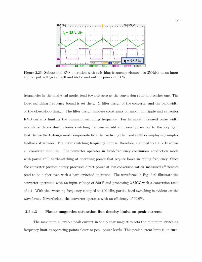
42
Figure 2.26: Suboptimal ZVS operation with switching frequency clamped to 350 kHz at an inputand output voltages of 250 and 550 V and output power of 3 kW
frequencies in the analytical model tend towards zero as the conversion ratio approaches one. The
lower switching frequency bound is set the L, C filter design of the converter and the bandwidth
of the closed-loop design. The filter design imposes constraints on maximum ripple and capacitor
RMS currents limiting the minimum switching frequency. Furthermore, increased pulse width
modulator delays due to lower switching frequencies add additional phase lag to the loop gain
that the feedback design must compensate by either reducing the bandwidth or employing complex
feedback structures. The lower switching frequency limit is, therefore, clamped to 100 kHz across
all converter modules. The converter operates in fixed-frequency continuous conduction mode
with partial/full hard-switching at operating points that require lower switching frequency. Since
the converter predominantly processes direct power at low conversion ratios, measured efficiencies
tend to be higher even with a hard-switched operation. The waveforms in Fig. 2.27 illustrate the
converter operation with an input voltage of 350 V and processing 3.8 kW with a conversion ratio
of 1.1. With the switching frequency clamped to 100 kHz, partial hard-switching is evident on the
waveforms. Nevertheless, the converter operates with an efficiency of 99.6%.
2.5.4.3 Planar magnetics saturation flux-density limits on peak currents
The maximum allowable peak current in the planar magnetics sets the minimum switching
frequency limit at operating points closer to peak power levels. This peak current limit is, in turn,
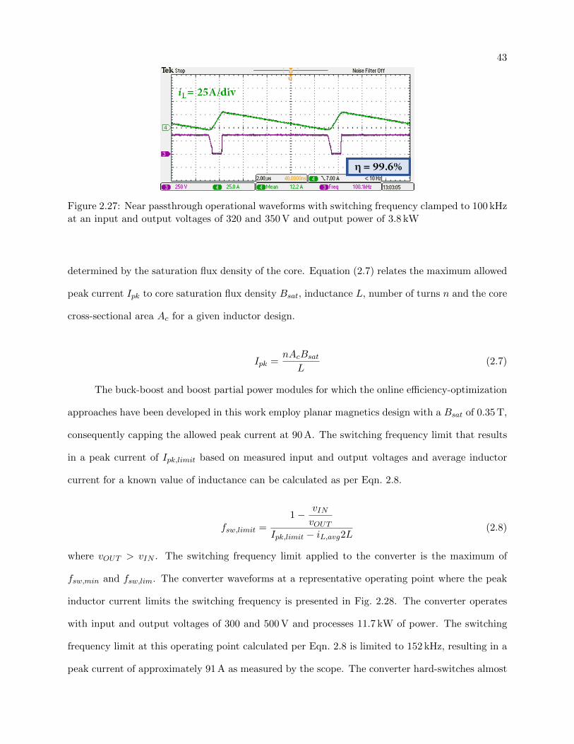
43
Figure 2.27: Near passthrough operational waveforms with switching frequency clamped to 100 kHzat an input and output voltages of 320 and 350 V and output power of 3.8 kW
determined by the saturation flux density of the core. Equation (2.7) relates the maximum allowed
peak current Ipk to core saturation flux density Bsat, inductance L, number of turns n and the core
cross-sectional area Ac for a given inductor design.
Ipk =nAcBsat
L(2.7)
The buck-boost and boost partial power modules for which the online efficiency-optimization
approaches have been developed in this work employ planar magnetics design with a Bsat of 0.35 T,
consequently capping the allowed peak current at 90 A. The switching frequency limit that results
in a peak current of Ipk,limit based on measured input and output voltages and average inductor
current for a known value of inductance can be calculated as per Eqn. 2.8.
fsw,limit =1− vIN
vOUTIpk,limit − iL,avg2L
(2.8)
where vOUT > vIN . The switching frequency limit applied to the converter is the maximum of
fsw,min and fsw,lim. The converter waveforms at a representative operating point where the peak
inductor current limits the switching frequency is presented in Fig. 2.28. The converter operates
with input and output voltages of 300 and 500 V and processes 11.7 kW of power. The switching
frequency limit at this operating point calculated per Eqn. 2.8 is limited to 152 kHz, resulting in a
peak current of approximately 91 A as measured by the scope. The converter hard-switches almost

44
entirely and operates with an efficiency of 98.5%.
Figure 2.28: Peak-current limited operation with the switching frequency clamped to a value(152 kHz) that results in the peak inductor current not exceeding 90 A. The converter operateswith input and output voltages of 300 and 600 V and output power of 11.7 kW
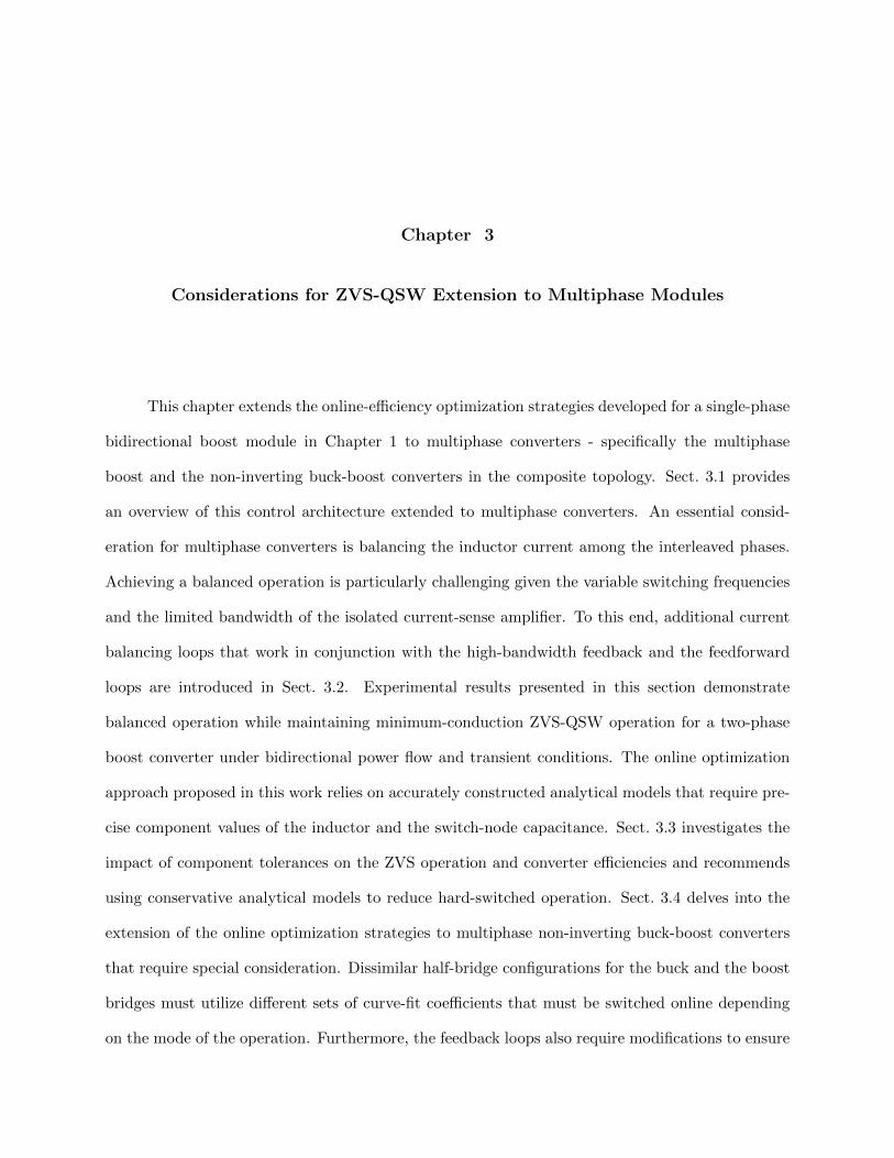
Chapter 3
Considerations for ZVS-QSW Extension to Multiphase Modules
This chapter extends the online-efficiency optimization strategies developed for a single-phase
bidirectional boost module in Chapter 1 to multiphase converters - specifically the multiphase
boost and the non-inverting buck-boost converters in the composite topology. Sect. 3.1 provides
an overview of this control architecture extended to multiphase converters. An essential consid-
eration for multiphase converters is balancing the inductor current among the interleaved phases.
Achieving a balanced operation is particularly challenging given the variable switching frequencies
and the limited bandwidth of the isolated current-sense amplifier. To this end, additional current
balancing loops that work in conjunction with the high-bandwidth feedback and the feedforward
loops are introduced in Sect. 3.2. Experimental results presented in this section demonstrate
balanced operation while maintaining minimum-conduction ZVS-QSW operation for a two-phase
boost converter under bidirectional power flow and transient conditions. The online optimization
approach proposed in this work relies on accurately constructed analytical models that require pre-
cise component values of the inductor and the switch-node capacitance. Sect. 3.3 investigates the
impact of component tolerances on the ZVS operation and converter efficiencies and recommends
using conservative analytical models to reduce hard-switched operation. Sect. 3.4 delves into the
extension of the online optimization strategies to multiphase non-inverting buck-boost converters
that require special consideration. Dissimilar half-bridge configurations for the buck and the boost
bridges must utilize different sets of curve-fit coefficients that must be switched online depending
on the mode of the operation. Furthermore, the feedback loops also require modifications to ensure
46
a smooth transition between the buck and the boost modes of operation. The minimum-conduction
ZVS-QSW operation in all four possible modes of the multiphase buck-boost converter operation is
validated through experimental results. In Sect. 3.5, the minimum-conduction ZVS-QSW range of
the multiphase converters is extended by employing a frequency-based phase-shedding technique.
In contrast to conventional power-based phase shedding that adjusts the number of operational
phases based on the processed power, the frequency-based technique looks at the converter switch-
ing frequency as a measure for phase shedding. This approach drastically reduces the number
of phase-shedding operations simplifying control and improving system reliability while achieving
efficiency improvements comparable with conventional phase shedding techniques. The impact of
the frequency-based phase shedding technique is contrasted with the conventional approach by
extrapolating the measured efficiency of a single-phase converter to a mutliphase operation.
3.1 Overview of the online-optimization control strategy extension to mul-
tiphase modules
Before extending the online-efficiency optimization control strategy proposed in Chapter 2
to multiphase converters, a survey of existing control strategies for variable timing-parameter ZVS
operation for multiphase converters is presented. Multiphase converters operate in an interleaved
mode that reduces the overall ripple on the output current and voltage, significantly reducing the
filter capacitance requirement [57, 69, 94]. This interleaving requires phase-shifted operation with
identical switching frequency for all the phases, making the extension of analog circuitry-based
ZVS approaches to multiphase converters particularly challenging. Analog approaches nevertheless
have been demonstrated in [8, 84] with [84] employing both zero-current and zero-voltage detec-
tion circuits while [8] utilizes peak current detection to achieve variable-frequency and dead-time
ZVS operation in forward power flow. Digital approaches to ZVS-QSW in multiphase convert-
ers have been demonstrated with lookup tables [58], constant SR turn-off current [10], and single
timing-parameter adjustments [28, 30, 56]. These approaches typically suffer limitations similar to
those discussed in the review of single-phase approaches in Chapter 2 - they are unable to achieve

47
minimum-conduction ZVS-QSW operation over a wide range.
Figure 3.1: Controller architecture includes a feedback loop responsible for the output voltageregulation and a feed-forward loop that implements the online efficiency optimization.
The online efficiency-optimization control strategy that achieves wide-range minimum-conduction
ZVS-QSW operation developed for a single half-bridge module in Chapter 2 is extended to multiple
phases in Fig. 3.1. Theoretically speaking, this extension is relatively straightforward. The feed-
back loop is modified to use independent inner average-current loops that ensure current balancing
among the phases. The voltage and current digital compensators follow the same single-phase design
except that the voltage compensator needs to account for maximum phase delay due to interleaved
execution of the phase current compensators of the nth last phase. Under ideal circumstances, the
feed-forward loop assumes a balanced interleave operation and utilizes the sensed average current
from any one of the phases for the curve-fitting. All phases operate with the same curve-fit switch-
ing frequency and forced natural-ZVS dead-time values. An additional phase-shift adjustment
block operating at the same rate as the feed-forward loop ensures balanced interleaved operation
by adjusting the pulse-width modulator phase-shift registers for the follower phases (phases 2 to n)
with the applied converter switching frequency. The analytical models and strategies for curve-fit
implementation and extension to reverse power flow remain the same as in Chapter 2.

48
3.2 Balancing the average inductor currents between the interleaved phases
3.2.1 Impact of current-sensor bandwidth on balanced operation
The idealized extension of the online efficiency-optimization control strategy to multiphase
converters presented in Fig. 3.1 assumes perfect balancing of the inductor current among the in-
terleaved phases. This assumption is typically not valid since asymmetry between the phases due
to component tolerances and timing mismatches (controller, gate-driver) results in imbalances in
the average inductor current between the phases [27,41,77,81,88]. Unbalanced operation not only
leads to increased ripple and conduction losses but also complicates the feed-forward loop imple-
mentation. The feed-forward loop can no longer assume balanced operation and pick an average
current value for fitting from an arbitrary phase lest a lower average value results in hard-switched
operation in other phases. Various digital balancing techniques have been explored in the litera-
ture, including techniques that employ individual phase current sensors and control loops [2,8] and
sensorless approaches [3,46]. Since the multiphase converters in this work operate over wide ranges
encompassing optimal and suboptimal ZVS and hard-switching, in addition to online adjusting the
number of phases, balancing techniques with individual sensors is preferable.
Figure 3.2: Isolated current-sense amplifier: (a) circuit diagram, and (b) magnitude plot of mea-sured transfer function vy/vx
The use of planar magnetics [31] and a meticulous layout design with a high degree of sym-
metry between the phases [56] can reduce current imbalances to a great extent. These strategies,
however, cannot compensate for current sharing imbalances arising from the current sensor itself.
Isolated current sensing strategies commonly employed in such high-frequency, high-power applica-
tions [54,79] operate with limited bandwidth. The inductor current-sensing circuit for each phase,

49
reproduced from Chapter 2 in Fig. 3.2(a), consists of a shunt-based isolated current-sense amplifier
followed by a differential amplifier. The differential amplifier output provides the sensed inductor
current to the feedback loop. A low-pass filtered version of this output provides an average inductor
current value to the feed-forward loop through a different microcontroller A/D channel. The mag-
nitude plot of the measured feedback sensing circuitry transfer-function (vy/vx) from the isolated
amplifier input to the non-isolated differential amplifier output for the four phases of the multiphase
boost converter is shown in Fig. 3.2(b). The −3 dB frequency of the individual current sensing cir-
cuit lies in the 700 to 900 kHz range. This cutoff-frequency range occurs in the same decade as the
fundamental frequency component of the inductor currents that lies in the 100 to 400 kHz range.
Depending on the duty cycle, the inductor currents may have significant harmonic components
that extend up to and beyond the sensor’s −3 dB range, resulting in operating point-dependent
distortion in the sensed signal. Furthermore, minor differences in the current sensor frequency
response in this range distort the individual phase currents by different amounts resulting in large
imbalances in the currents.
Figure 3.3: (a) Inductor current and (b) current-sensor output waveforms during unbalanced op-eration in a four-phase boost at 200 V to 400 V conversion with 2.8 kW
The inductor current waveforms for the four-phase boost converter under unbalanced oper-
ation at a specific operating point are shown in Fig. 3.3. The converter operates with input and
output voltages of 200 V and 400 V and processes an overall output power of 2.8 kW. All phases
operate in an interleaved manner with a switching frequency of 290 kHz, but the average value of
phase two inductor current is significantly lower than the other phases. The average current is, in

50
fact, negative, resulting in the power processed by phase two being entirely circulatory without any
active contribution to the output power. The measured inductor current signal waveforms for all
phases presented in Fig. 3.3(b) highlight the impact of the current sensor in driving the imbalances.
The distortion in the sensed signal due to current sensor bandwidth limitations is visible. The small
spikes in each signal indicate the instant the controller analog-to-digital converter samples the in-
ductor current. It may be observed that the sampling points are perfectly interleaved and occur
at relatively the same instants in the switching period of the corresponding phase. Although, the
digital current-controller loops function as intended and regulate the sampled points to a common
current reference generated by the outer voltage loop, there is little correlation between the sampled
value and the actual average current in the corresponding inductors due to the waveform distortion.
Therefore, the controller cannot detect the significantly reduced average current in the phase two
inductor, which operates with increased distortion.
3.2.2 Current-balancing compensators
Attempts to achieve balanced operation through software calibration of the measured cur-
rent sensors output generally prove futile due to the operating-point-dependent behavior of the
sensor. Figure 3.4 illustrates a more elegant approach using current-balancing compensators that
operate directly on the sensed average current measurements. The average current measurement
provided as an input to the feed-forward loop utilizes a filtered version of the same isolated-amplifier
current-sensor output by employing additional low-pass filtering. Essentially, the current-balancing
compensators strive to equalize all the measured average current values by making minor correc-
tions to individual inner current references. The common reference to the balancing compensator is
the calculated average of all the measured average phase currents. By appropriately adjusting the
inner current loop reference, each balancing compensator drives the error between the measured
average current of the respective phase and the calculated average reference to zero.
The current-balancing compensators are designed to operate at a bandwidth lower than both
the inner current and the outer voltage compensators to prevent interaction with the loops and

51
Figure 3.4: Low-bandwidth current-balancing compensators adjust current references for each phaseto equalize all the sensed average current measurements
modify the transient performance of the converter. A 100 Hz bandwidth for the current-balancing
compensators provides a sufficient margin from the voltage compensator while ensuring that the
average currents are adequately balanced for the 6 Hz feed-forward loop. The balancing compen-
sators are simple to design since the uncompensated loop-gain Tu from the balance compensator
output to the average current feedback in phase is simply the response of the low-pass filter and is
given as-
Tu =1
1 +s
wLPF
(3.1)
where wLPF is the low-pass-filter corner frequency in radians. The design consists of a discretized
proportional-integral compensator and requires no additional sensor other than the ones already
present in the system. The converter waveforms at the same operating point from Fig. 3.3 are
presented in Fig. 3.5(a) with the addition of the current-balancing compensators. The maximum
deviation of 3.10 A from the overall average input current of 3.6 A is around 13%. The converter
also operates with a switching frequency clamped to the maximum value 350 kHz, as expected
at this low-power operating point. The output waveforms from the current sensors are produced
in Fig. 3.5. The current-balancing loops are also directly extended to bidirectional power flow.
The two-phase boost converter waveforms with input and output voltages of 350 and 500 V and
10kW output power in both forward and reverse directions are shown in Fig. 3.6(a) and Fig. 3.6(b),
respectively. The waveforms indicate balanced operation in both directions of power flow with feed-
forward adjustment of timing parameters to achieve minimum-conduction ZVS-QSW operation.

52
Figure 3.5: (a) Inductor current and (b) current-sensor output waveforms during balanced operationin a four-phase boost at 200 V to 400 V conversion with 2.8 kW
Figure 3.6: Balanced two-phase boost converter operation with input and output voltages of 350 Vand 500 V and 10 kW processed power in (a) forward and (b) reverse operation
Figure 3.7 presents the transient-response waveforms for a two-phase boost converter during
a step-change in the output voltage reference from 400V to 500V with a corresponding change in
output power from 4 kW to 14kW. The outer voltage and inner current feedback loops ensure
fast settling times of approximately 100us after the step change, with the current-balancing loops
keeping the inductor currents between the phases well-balanced. The feed-forward loop, now (jus-
tifiably) assuming that the inductor currents are balanced, adjusts the converter timing parameters
based on the average inductor-current measurement of phase 1 to achieve minimum-conduction
ZVS-QSW operation, as confirmed by the waveform inserts. Before the transient is applied, the
converter operates with optimal timing parameters of 239.5 kHz and 200 ns with a measured steady-
state efficiency of 99.3%. Post application of the step-reference transient, the converter settles at
the new optimal values of 254.2 kHz and 225 ns over around 100 ms time interval to a new steady
state with a measured efficiency of 99.2%.
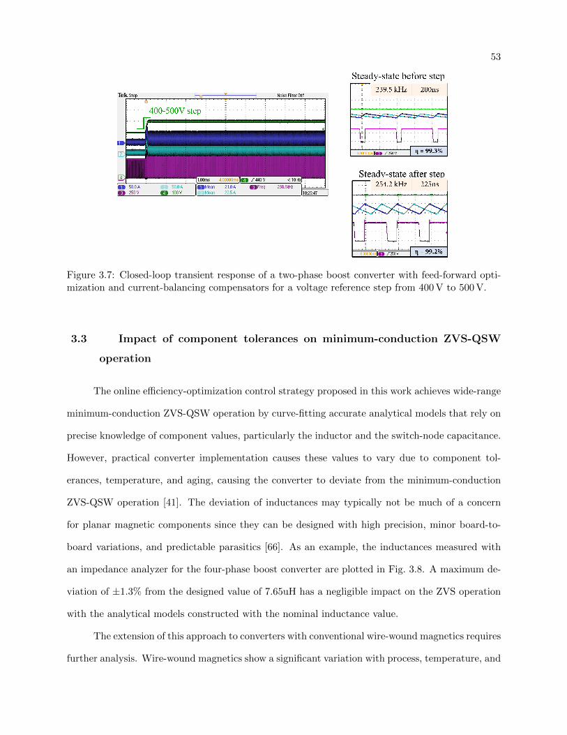
53
Figure 3.7: Closed-loop transient response of a two-phase boost converter with feed-forward opti-mization and current-balancing compensators for a voltage reference step from 400 V to 500 V.
3.3 Impact of component tolerances on minimum-conduction ZVS-QSW
operation
The online efficiency-optimization control strategy proposed in this work achieves wide-range
minimum-conduction ZVS-QSW operation by curve-fitting accurate analytical models that rely on
precise knowledge of component values, particularly the inductor and the switch-node capacitance.
However, practical converter implementation causes these values to vary due to component tol-
erances, temperature, and aging, causing the converter to deviate from the minimum-conduction
ZVS-QSW operation [41]. The deviation of inductances may typically not be much of a concern
for planar magnetic components since they can be designed with high precision, minor board-to-
board variations, and predictable parasitics [66]. As an example, the inductances measured with
an impedance analyzer for the four-phase boost converter are plotted in Fig. 3.8. A maximum de-
viation of ±1.3% from the designed value of 7.65uH has a negligible impact on the ZVS operation
with the analytical models constructed with the nominal inductance value.
The extension of this approach to converters with conventional wire-wound magnetics requires
further analysis. Wire-wound magnetics show a significant variation with process, temperature, and
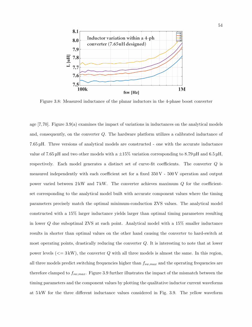
54
Figure 3.8: Measured inductance of the planar inductors in the 4-phase boost converter
age [7,70]. Figure 3.9(a) examines the impact of variations in inductances on the analytical models
and, consequently, on the converter Q. The hardware platform utilizes a calibrated inductance of
7.65 µH. Three versions of analytical models are constructed - one with the accurate inductance
value of 7.65 µH and two other models with a ±15% variation corresponding to 8.79 µH and 6.5 µH,
respectively. Each model generates a distinct set of curve-fit coefficients. The converter Q is
measured independently with each coefficient set for a fixed 350 V - 500 V operation and output
power varied between 2 kW and 7 kW. The converter achieves maximum Q for the coefficient-
set corresponding to the analytical model built with accurate component values where the timing
parameters precisely match the optimal minimum-conduction ZVS values. The analytical model
constructed with a 15% larger inductance yields larger than optimal timing parameters resulting
in lower Q due suboptimal ZVS at each point. Analytical model with a 15% smaller inductance
results in shorter than optimal values on the other hand causing the converter to hard-switch at
most operating points, drastically reducing the converter Q. It is interesting to note that at lower
power levels (<= 3 kW), the converter Q with all three models is almost the same. In this region,
all three models predict switching frequencies higher than fsw,max and the operating frequencies are
therefore clamped to fsw,max. Figure 3.9 further illustrates the impact of the mismatch between the
timing parameters and the component values by plotting the qualitative inductor current waveforms
at 5 kW for the three different inductance values considered in Fig. 3.9. The yellow waveform
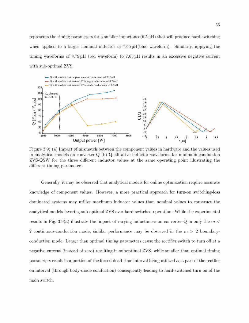
55
represents the timing parameters for a smaller inductance(6.5 µH) that will produce hard-switching
when applied to a larger nominal inductor of 7.65 µH(blue waveform). Similarly, applying the
timing waveforms of 8.79 µH (red waveform) to 7.65 µH results in an excessive negative current
with sub-optimal ZVS.
Figure 3.9: (a) Impact of mismatch between the component values in hardware and the values usedin analytical models on converter-Q (b) Qualitative inductor waveforms for minimum-conductionZVS-QSW for the three different inductor values at the same operating point illustrating thedifferent timing parameters
Generally, it may be observed that analytical models for online optimization require accurate
knowledge of component values. However, a more practical approach for turn-on switching-loss
dominated systems may utilize maximum inductor values than nominal values to construct the
analytical models favoring sub-optimal ZVS over hard-switched operation. While the experimental
results in Fig. 3.9(a) illustrate the impact of varying inductances on converter-Q in only the m <
2 continuous-conduction mode, similar performance may be observed in the m > 2 boundary-
conduction mode. Larger than optimal timing parameters cause the rectifier switch to turn off at a
negative current (instead of zero) resulting in suboptimal ZVS, while smaller than optimal timing
parameters result in a portion of the forced dead-time interval being utilized as a part of the rectfier
on interval (through body-diode conduction) consequently leading to hard-switched turn on of the
main switch.
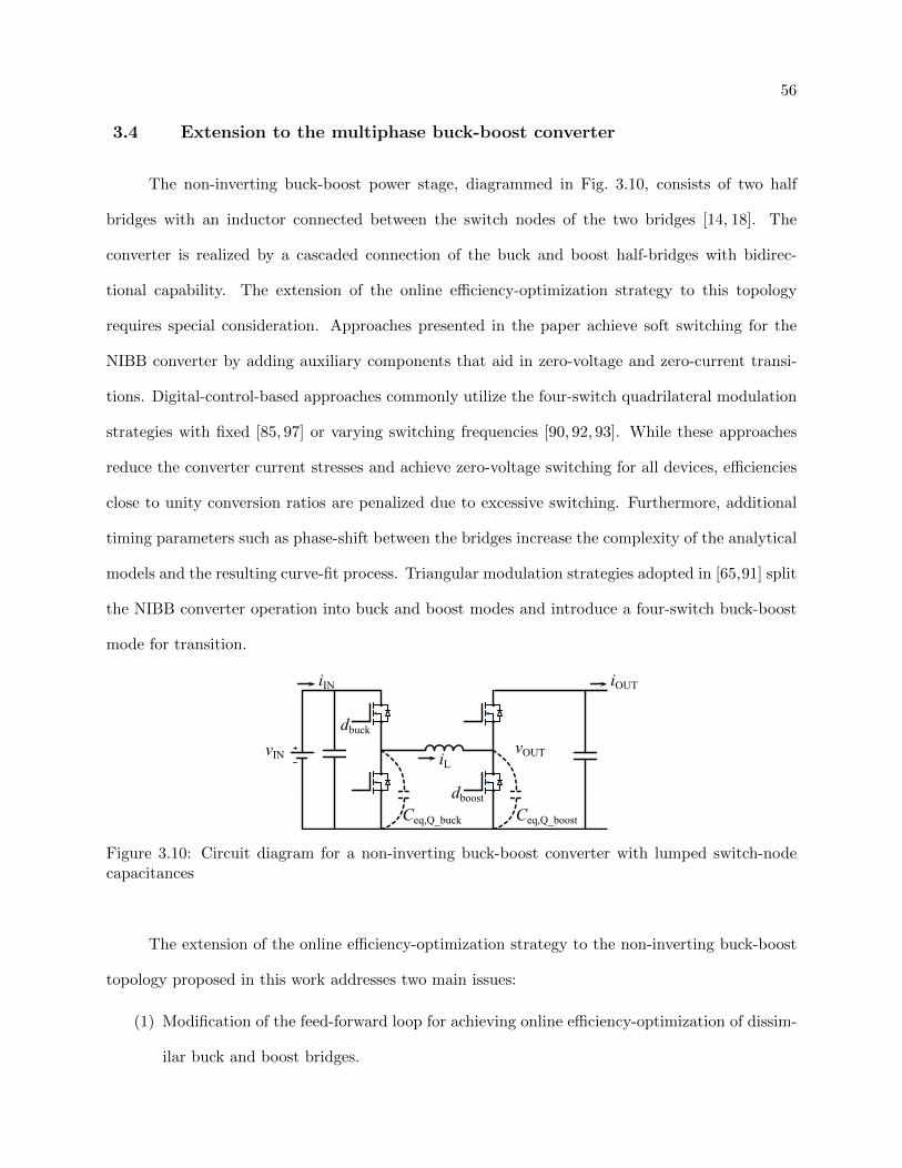
56
3.4 Extension to the multiphase buck-boost converter
The non-inverting buck-boost power stage, diagrammed in Fig. 3.10, consists of two half
bridges with an inductor connected between the switch nodes of the two bridges [14, 18]. The
converter is realized by a cascaded connection of the buck and boost half-bridges with bidirec-
tional capability. The extension of the online efficiency-optimization strategy to this topology
requires special consideration. Approaches presented in the paper achieve soft switching for the
NIBB converter by adding auxiliary components that aid in zero-voltage and zero-current transi-
tions. Digital-control-based approaches commonly utilize the four-switch quadrilateral modulation
strategies with fixed [85, 97] or varying switching frequencies [90, 92, 93]. While these approaches
reduce the converter current stresses and achieve zero-voltage switching for all devices, efficiencies
close to unity conversion ratios are penalized due to excessive switching. Furthermore, additional
timing parameters such as phase-shift between the bridges increase the complexity of the analytical
models and the resulting curve-fit process. Triangular modulation strategies adopted in [65,91] split
the NIBB converter operation into buck and boost modes and introduce a four-switch buck-boost
mode for transition.
Figure 3.10: Circuit diagram for a non-inverting buck-boost converter with lumped switch-nodecapacitances
The extension of the online efficiency-optimization strategy to the non-inverting buck-boost
topology proposed in this work addresses two main issues:
(1) Modification of the feed-forward loop for achieving online efficiency-optimization of dissim-
ilar buck and boost bridges.
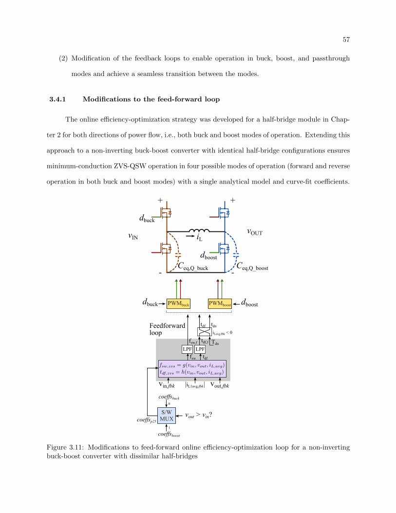
57
(2) Modification of the feedback loops to enable operation in buck, boost, and passthrough
modes and achieve a seamless transition between the modes.
3.4.1 Modifications to the feed-forward loop
The online efficiency-optimization strategy was developed for a half-bridge module in Chap-
ter 2 for both directions of power flow, i.e., both buck and boost modes of operation. Extending this
approach to a non-inverting buck-boost converter with identical half-bridge configurations ensures
minimum-conduction ZVS-QSW operation in four possible modes of operation (forward and reverse
operation in both buck and boost modes) with a single analytical model and curve-fit coefficients.
Figure 3.11: Modifications to feed-forward online efficiency-optimization loop for a non-invertingbuck-boost converter with dissimilar half-bridges

58
The drive-cycle-based multiobjective optimization approach emphasizes both the converter
reliability and efficiency for realizing the composite converter topology [34]. Given that a buck
mode of operation for the buck-boost topology occurs for a relatively small portion of the drive
cycle, an asymmetric configuration with a 1-die buck and 2-die boost offers the optimal tradeoff
between overall system reliability and efficiency. The feed-forward loop, accordingly modified as
per Fig. 3.11, utilizes two independent analytical models with a distinct set of coefficients for the
buck and the boost modes of operation. A software multiplexer provides the right coefficient-set
to the feed-forward loop depending on the mode of operation as determined by the relationship
between input and output voltages. As detailed in the subsequent section, independent feedback
loops for the buck and the boost half-bridges ensure the converter operates in one of the three
modes - buck, boost, or passthrough.
Figure 3.12: Buck and boost mode operational waveforms at identical operating conditions withdiffering die configurations
The waveforms for a single-phase non-inverting buck-boost converter operating with identical
input/output voltages and power levels are presented in Fig. 3.12. In the buck mode, the converter
steps down an input voltage of 350V to 200V while it steps up 200 V to 350 V in boost mode.
The converter processes an output power of 5.4 kW in both cases. The 2-die boost mode requires
higher timing parameter values than the 1-die buck mode to achieve minimum-conduction ZVS-
QSW operation for the same operating conditions. The converter also operates a slightly higher
efficiency in the boost mode due to the lower on-resistances of the two-die devices.

59
3.4.2 Modifications to the feedback loops
Typical approaches for controlling the non-inverting buck-boost converter near passthrough
(input and output voltages are close to equal in magnitude) and achieving buck-boost transitions
involve the addition of a buck-boost operating mode wherein all four devices are switched [38,52,65].
These approaches may not suit the composite converter topology since the buck-boost converter
is intentionally operated in the passthrough region for extended periods in different composite
converter operating modes. A complete passthrough operation with only the top switches of all
bridges turned on is desirable for reducing the control complexity and improving efficiency.
Figure 3.13: Single-phase compensator structure for the buck-boost converter with independentloops for the buck and the boost bridges
Employing independent compensator structures for the buck and the boost bridges, as shown
in Fig. 3.13, can achieve a complete passthrough with seamless transition. The outer voltage com-
pensators to both loops are provided the same output voltage reference with a small differential
component of V ∗. This differential component ensures that only one set of loops and the corre-
sponding bridge is active. The other bridge is naturally driven to passthrough operation with the
top switch turned on. Equations (3.2)-(3.4) govern the buck-boost converter operation for a given
input voltage and output voltage reference.
vIN < VOUT,ref − V ∗, BoostMode (3.2)
vIN > VOUT,ref + V ∗, BuckMode (3.3)
VOUT,ref − V ∗ <= vIN <= VOUT,ref + V ∗, Passthrough (3.4)
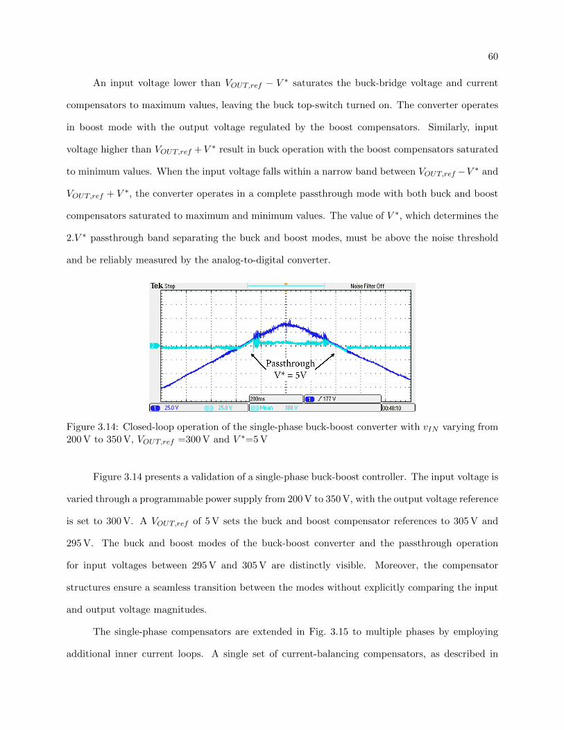
60
An input voltage lower than VOUT,ref − V ∗ saturates the buck-bridge voltage and current
compensators to maximum values, leaving the buck top-switch turned on. The converter operates
in boost mode with the output voltage regulated by the boost compensators. Similarly, input
voltage higher than VOUT,ref +V ∗ result in buck operation with the boost compensators saturated
to minimum values. When the input voltage falls within a narrow band between VOUT,ref −V ∗ and
VOUT,ref + V ∗, the converter operates in a complete passthrough mode with both buck and boost
compensators saturated to maximum and minimum values. The value of V ∗, which determines the
2.V ∗ passthrough band separating the buck and boost modes, must be above the noise threshold
and be reliably measured by the analog-to-digital converter.
Figure 3.14: Closed-loop operation of the single-phase buck-boost converter with vIN varying from200 V to 350 V, VOUT,ref =300 V and V ∗=5 V
Figure 3.14 presents a validation of a single-phase buck-boost controller. The input voltage is
varied through a programmable power supply from 200 V to 350 V, with the output voltage reference
is set to 300 V. A VOUT,ref of 5 V sets the buck and boost compensator references to 305 V and
295 V. The buck and boost modes of the buck-boost converter and the passthrough operation
for input voltages between 295 V and 305 V are distinctly visible. Moreover, the compensator
structures ensure a seamless transition between the modes without explicitly comparing the input
and output voltage magnitudes.
The single-phase compensators are extended in Fig. 3.15 to multiple phases by employing
additional inner current loops. A single set of current-balancing compensators, as described in

61
Figure 3.15: Compensator structure for the three-phase non-inverting buck-boost compensator withcurrent-balancing compensators
Table 3.1: Nominal operating points and corresponding analytical values for validation of theonline efficiency-optimization strategy with bidirectional power flow of the two-phase non-invertingbuck-boost converter
Device config. |Pout| per phase fsw tdf
1-die half-bridge 5 kW 148.8 kHz 270 ns
2-die half-bridge 6.5 kW 248.3 kHz 315 ns
Section 3.2, adjust the current references to both the buck and boost inner current loops to achieve
a balanced interleaved operation.
Figure 3.16(a) - (d) demonstrate online efficiency-optimization for a two-phase non-inverting
buck-boost converter for the four operating modes. Fig. 3.16(a) and (b) plot the converter wave-
forms for the forward and reverse power flow of the 1-die half-bridge. Fig. 3.16(c) and (d) plot the
corresponding waveforms for the operation of the 2-die half-bridge with Table 3.1 listing the nom-
inal processed power and analytical timing parameters for both sets of waveforms. The switching
cell circuits accompanying the waveforms illustrate the power-flow direction and input/output volt-
ages. The online-adjusted timing parameters marked on the plots—sensitive to load adjustments,
processed power, and sensor calibration—deviate from the expected nominal value yet achieve near
minimum-conduction ZVS-QSW operation with high efficiencies at considered operating points. In
conjunction with the feedback compensators, the current-balancing loops enable balanced inter-
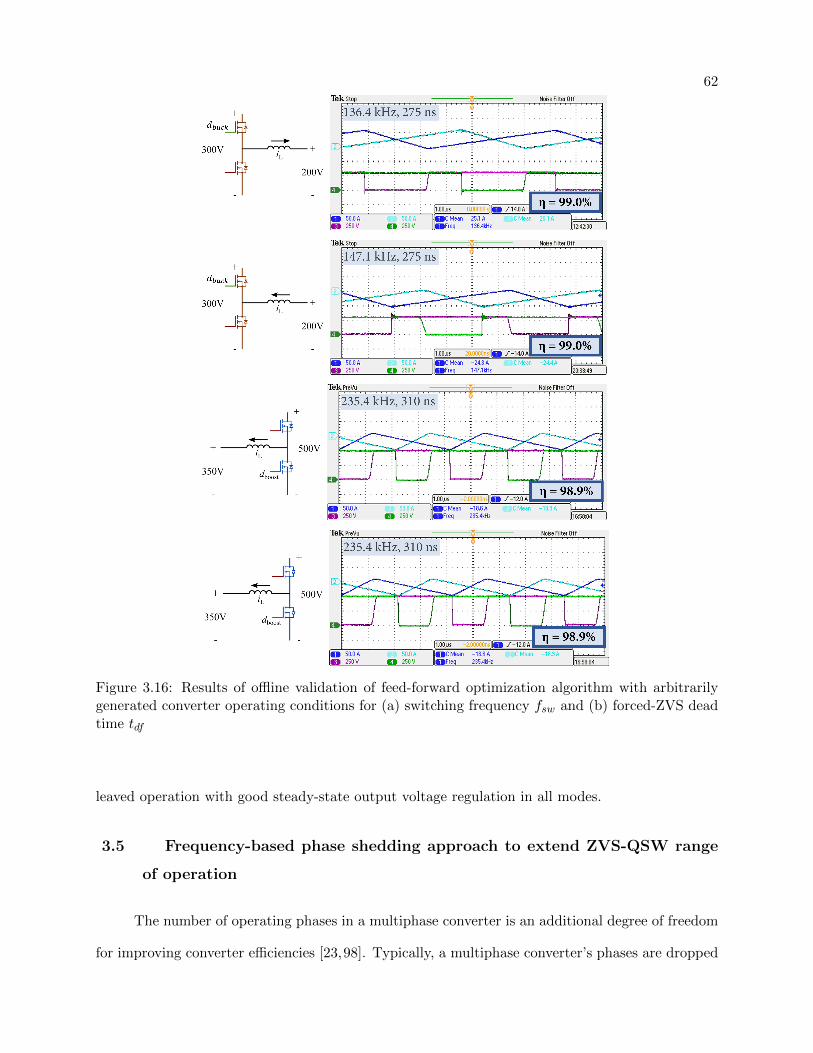
62
Figure 3.16: Results of offline validation of feed-forward optimization algorithm with arbitrarilygenerated converter operating conditions for (a) switching frequency fsw and (b) forced-ZVS deadtime tdf
leaved operation with good steady-state output voltage regulation in all modes.
3.5 Frequency-based phase shedding approach to extend ZVS-QSW range
of operation
The number of operating phases in a multiphase converter is an additional degree of freedom
for improving converter efficiencies [23,98]. Typically, a multiphase converter’s phases are dropped
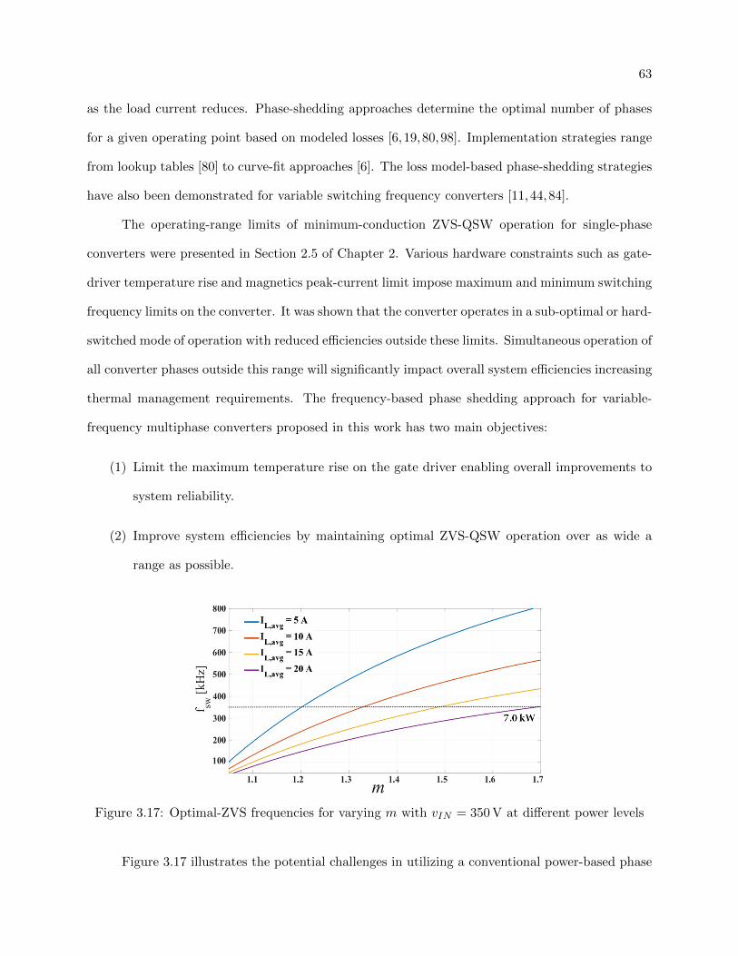
63
as the load current reduces. Phase-shedding approaches determine the optimal number of phases
for a given operating point based on modeled losses [6,19,80,98]. Implementation strategies range
from lookup tables [80] to curve-fit approaches [6]. The loss model-based phase-shedding strategies
have also been demonstrated for variable switching frequency converters [11,44,84].
The operating-range limits of minimum-conduction ZVS-QSW operation for single-phase
converters were presented in Section 2.5 of Chapter 2. Various hardware constraints such as gate-
driver temperature rise and magnetics peak-current limit impose maximum and minimum switching
frequency limits on the converter. It was shown that the converter operates in a sub-optimal or hard-
switched mode of operation with reduced efficiencies outside these limits. Simultaneous operation of
all converter phases outside this range will significantly impact overall system efficiencies increasing
thermal management requirements. The frequency-based phase shedding approach for variable-
frequency multiphase converters proposed in this work has two main objectives:
(1) Limit the maximum temperature rise on the gate driver enabling overall improvements to
system reliability.
(2) Improve system efficiencies by maintaining optimal ZVS-QSW operation over as wide a
range as possible.
Figure 3.17: Optimal-ZVS frequencies for varying m with vIN = 350 V at different power levels
Figure 3.17 illustrates the potential challenges in utilizing a conventional power-based phase
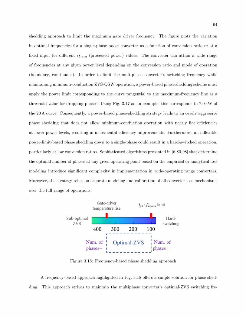
64
shedding approach to limit the maximum gate driver frequency. The figure plots the variation
in optimal frequencies for a single-phase boost converter as a function of conversion ratio m at a
fixed input for different iL,zvg (processed power) values. The converter can attain a wide range
of frequencies at any given power level depending on the conversion ratio and mode of operation
(boundary, continuous). In order to limit the multiphase converter’s switching frequency while
maintaining minimum-conduction ZVS-QSW operation, a power-based phase shedding scheme must
apply the power limit corresponding to the curve tangential to the maximum-frequency line as a
threshold value for dropping phases. Using Fig. 3.17 as an example, this corresponds to 7.0 kW of
the 20 A curve. Consequently, a power-based phase-shedding strategy leads to an overly aggressive
phase shedding that does not allow minimum-conduction operation with nearly flat efficiencies
at lower power levels, resulting in incremental efficiency improvements. Furthermore, an inflexible
power-limit-based phase shedding down to a single-phase could result in a hard-switched operation,
particularly at low conversion ratios. Sophisticated algorithms presented in [6,80,98] that determine
the optimal number of phases at any given operating point based on the empirical or analytical loss
modeling introduce significant complexity in implementation in wide-operating range converters.
Moreover, the strategy relies on accurate modeling and calibration of all converter loss mechanisms
over the full range of operations.
Figure 3.18: Frequency-based phase shedding approach
A frequency-based approach highlighted in Fig. 3.18 offers a simple solution for phase shed-
ding. This approach strives to maintain the multiphase converter’s optimal-ZVS switching fre-
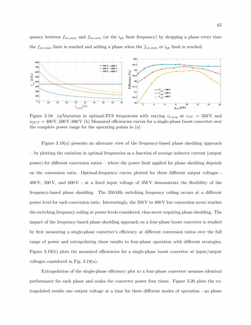
65
quency between fsw,max and fsw,min (or the ipk limit frequency) by dropping a phase every time
the fsw,max limit is reached and adding a phase when the fsw,min or ipk limit is reached.
Figure 3.19: (a)Variation in optimal-ZVS frequencies with varying iL,avg at vIN = 350 V andvOUT = 400 V, 500 V, 600 V (b) Measured efficiencies curves for a single-phase boost converter overthe complete power range for the operating points in (a)
Figure 3.19(a) presents an alternate view of the frequency-based phase shedding approach
—by plotting the variation in optimal frequencies as a function of average inductor current (output
power) for different conversion ratios —where the power limit applied for phase shedding depends
on the conversion ratio. Optimal-frequency curves plotted for three different output voltages -
400 V, 500 V, and 600 V - at a fixed input voltage of 350 V demonstrate the flexibility of the
frequency-based phase shedding. The 350 kHz switching frequency ceiling occurs at a different
power level for each conversion ratio. Interestingly, the 350 V to 400 V low conversion never reaches
the switching frequency ceiling at power levels considered, thus never requiring phase shedding. The
impact of the frequency-based phase shedding approach on a four-phase boost converter is studied
by first measuring a single-phase converter’s efficiency at different conversion ratios over the full
range of power and extrapolating these results to four-phase operation with different strategies.
Figure 3.19(b) plots the measured efficiencies for a single-phase boost converter at input/output
voltages considered in Fig. 3.19(a).
Extrapolation of the single-phase efficiency plot to a four-phase converter assumes identical
performance for each phase and scales the converter power four times. Figure 3.20 plots the ex-
trapolated results one output voltage at a time for three different modes of operation - no phase

66
Figure 3.20: Comparison of various phase-shedding strategies on a 4-phase boost converter withan input voltage of 350 V and output voltages of (a) 400 V, (b) 500 V and (c) 600 V
shedding (dashed line), power-based phase shedding with a 7.0 kW threshold (solid line), and
67
frequency-based phase shedding with a 350 kHz threshold. The converter power levels are assumed
to vary in the plot from right to left (high to low) so that the phases are shed one at a time as
indicated by the number of active phases on the curves corresponding to frequency and power-
based phase shedding operation. The frequency-based and power-based phase shedding approaches
are identical for the 600 V output voltage case in Fig. 3.20(a) since the 7.0 kW threshold at this
conversion ratio requires a 350 kHz optimum-ZVS frequency. In Fig. 3.20 plot for 500 V output
voltage, frequency-based phase shedding allows 4-ph operation over a broader output power range
with nearly flat efficiencies. The operational power range for three and four-phase operation is sim-
ilarly widened with efficiencies comparable to the power-based phase shedding approach applying
a fixed 7.0 kW threshold. The most significant impact of frequency-based phase shedding is on the
400 V output voltage plots in Fig. 3.20(c). Since the converter switching frequency never exceeds
350 kHz, frequency-based shedding allows four-phase operation through the entire range. This effi-
ciency closely matches the performance of the power-based phase shedding approach. Efficiencies
below 10kW of the four-phase converter drop sharply compared with the single-phase operation at
the same power levels. However, the magnitude of losses per phase is tiny and easily handled by
the thermal system rated for full power.
Frequency-based phase shedding limits maximum switching frequencies in multiphase con-
verters and strives to achieve minimum-conduction ZVS-QSW over as wide an operational range
as possible. The plots in Fig. 3.20 demonstrate that frequency-based phase-shedding and feed-
forward optimization results in optimal-ZVS operation at lower frequencies and approaches the
performance of power-based phase shedding with fewer transitions, thereby mitigating the impact
of temperature-cycling-based failure mechanisms [17,75].

Chapter 4
System-level Control Strategies and Mode Transitions
This chapter addresses system-level considerations for efficiency-optimized control of compos-
ite converters. Section 4.1 details the various operating modes for the given composite converter
topology, specifies the conditions for operation in every mode and addresses mode-transition imple-
mentation strategies. Section 4.2 presents the performance and closed-loop characterization of the
composite converter through different experimental setups, incorporating both module-level and
system-level efficiency optimization strategies.
4.1 Composite converter modes
Figure 4.1: A simplified circuit-diagram for the composite converter topology
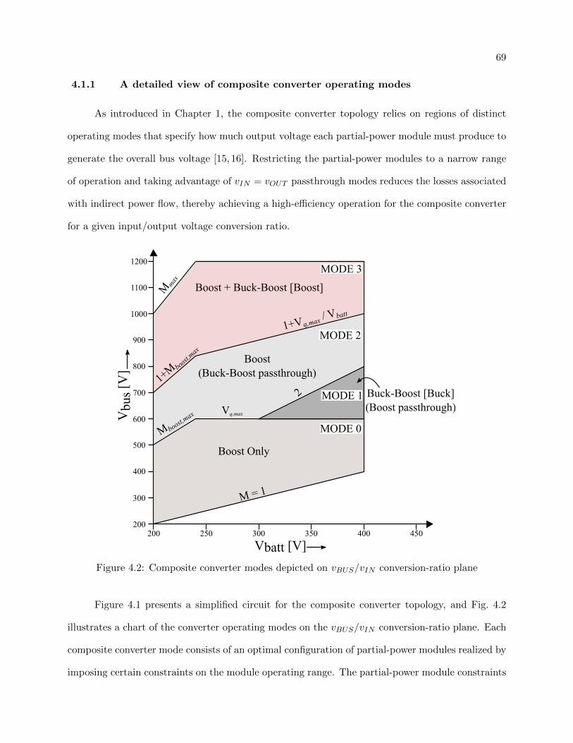
69
4.1.1 A detailed view of composite converter operating modes
As introduced in Chapter 1, the composite converter topology relies on regions of distinct
operating modes that specify how much output voltage each partial-power module must produce to
generate the overall bus voltage [15, 16]. Restricting the partial-power modules to a narrow range
of operation and taking advantage of vIN = vOUT passthrough modes reduces the losses associated
with indirect power flow, thereby achieving a high-efficiency operation for the composite converter
for a given input/output voltage conversion ratio.
Figure 4.2: Composite converter modes depicted on vBUS/vIN conversion-ratio plane
Figure 4.1 presents a simplified circuit for the composite converter topology, and Fig. 4.2
illustrates a chart of the converter operating modes on the vBUS/vIN conversion-ratio plane. Each
composite converter mode consists of an optimal configuration of partial-power modules realized by
imposing certain constraints on the module operating range. The partial-power module constraints

70
Table 4.1: Partial-power module constraints for realizing optimal composite converter operatingmodes
Parameter Description Value
Mboost,max Maximum conversion ratio for boost 2.5
Ndcx DCX fixed conversion ratio 1
Vq,max Maximum output voltage for each module 600 V
Mmax Maximum system conversion ratio (Vbus <= 1200 V) 5
mbuckboost Conversion-ratio range for buck-boost 0.5-2.5
listed in Table 4.1 are determined from the system/module-level loss modeling, reliability consider-
ations, and optimization performed in the topology synthesis step [34]. In addition to limiting the
modules’ operational ranges, the composite converter modes further optimize system efficiency by
ensuring that only one partial-power module switches in any mode with the other module/modules
turned off or operating in passthrough. With the 1:1 DCX functioning as a high-efficiency isolated
voltage follower to the buck-boost output, the composite converter output voltage is the sum of
the boost and the buck-boost output voltages.
The following paragraphs provide a detailed look at each composite converter mode, the
bounds and conditions for partial-power module operation in each mode.
4.1.1.1 MODE-0
Composite-converter MODE-0 is bounded by the maximum conversion ratio of the boost
converter and the maximum output voltage of a partial-power module. Within these bounds, the
boost converter provides the entire vBUS output, as shown in Fig. 4.3. The top stage produces
no output voltage since the buck-boost and the DCX inverter switches are turned off. The four
DCX-rectifier devices are turned-on to conduct the output current, minimizing conduction losses.
4.1.1.2 Composite converter passthrough mode and MODE-1
As mentioned previously, the composite converter output is the sum of the buck-boost and
boost converter output voltages. With both these converters operating in vIN = vOUT passthrough

71
Figure 4.3: Composite converter MODE-0
mode, the composite converter operates on the M = 2 line on the composite converter vBUS/vIN
plane with output twice the input voltage. The system efficiency is determined by the efficiency
of the DCX converter, which processes the entirety of the indirect power. Outside of MODE-0,
M = 2 composite passthrough operation shown in Fig. 4.4(a) results in the best overall composite
converter efficiencies over wide ranges.
For system conversion ratios lower than 2 for bus voltages exceeding the maximum per-module
output voltage capability vQ,max, the composite converter transition to MODE-1 diagrammed in
Fig. 4.4(b). The boost converter remains in passthrough with the buck-boost operating in the
buck-mode with conversion ratio M-1 to provide the remaining bus voltage (vBUS − vIN ).
Figure 4.4: (a) M = 2 composite converter passthrough mode (b) Composite converter MODE-1

72
4.1.1.3 MODE-2
As the system conversion ratio exceeds 2, the composite converter enters MODE-2 operation
when the bus voltage exceeds the maximum conversion ratio and output voltage capability of the
boost module alone. In MODE-2 —shown in Fig. 4.5 —the buck-boost converter transitions to
passthrough while the boost converter operates with the conversion ratio M − 1 to provide the
remaining output voltage (vBUS − vIN ).
It may be noted that operating the buck-boost converter in boost mode with the boost in
passthrough is an alternative configuration for the MODE-2. However, the minimum output power
requirements for ZVS operation of a conventionally modulated dual-active-bridge DCX topology
increases penalizing drive cycle efficiencies due to excessive hard-switched operation at low power
operating points [25]. A passthrough operation for the buck-boost lowering the ZVS requirements
for DCX is therefore preferable.
Figure 4.5: Composite converter MODE-2
4.1.1.4 MODE-3
The high system-conversion-ratio region of MODE-3 is the only mode where both the boost
and the buck-boost modules switch. The boost converter conversion ratio saturates to Mboost,max
(up to vq,max limit for the module voltage). The buck-boost converter operating in boost mode

73
provides the remaining output voltage. With module-level efficiency optimization strategies of
Chapters 2 and 3 in place for the partial-power modules, the boost and buck-boost converter exhibit
high efficiencies with minimum-conduction ZVS-QSW operation allowing the boost converter to
operate with a high conversion ratio and provide its maximum output capability at the majority
of the operating points. The
Figure 4.6: Composite converter MODE-3
4.1.2 Implementation of mode-transition algorithms
Table 4.2 summarizes the composite converter modes with the boundary conditions and
partial-power module references for each mode. As highlighted in Figure 4.7(a), the mode-transition
algorithm only runs on the boost and buck-boost modules and utilizes battery voltage and bus ref-
erence as inputs. Both converters independently measure the battery voltage vBATT while vBUS,ref
is supplied on the CAN bus through a central controller or another supervisory system. Based
on the boundary conditions in Table 4.2, the mode-transition algorithm generates the appropriate
modes and compensator voltage references for the module-level controllers. Appropriate clamps
on various references ensure that module-level and system-level operational limits are not violated.
The algorithm runs as a 100 Hz scheduled task in the main thread outside the ISR context.
The dual-active-bridge-based DCX module does not need to run the mode-transition algo-
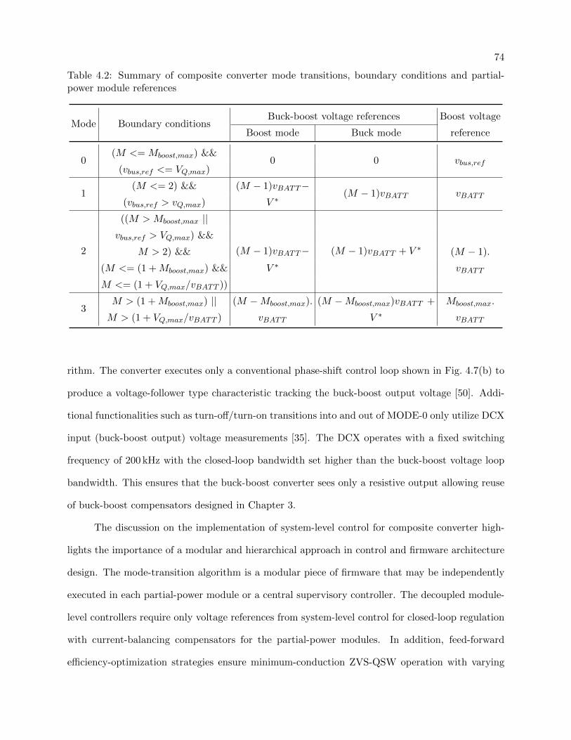
74
Table 4.2: Summary of composite converter mode transitions, boundary conditions and partial-power module references
Mode Boundary conditionsBuck-boost voltage references Boost voltage
Boost mode Buck mode reference
0(M <= Mboost,max) &&
0 0 vbus,ref(vbus,ref <= VQ,max)
1(M <= 2) && (M − 1)vBATT−
(M − 1)vBATT vBATT(vbus,ref > vQ,max) V ∗
2
((M > Mboost,max ||
(M − 1)vBATT− (M − 1)vBATT + V ∗vbus,ref > VQ,max) &&
M > 2) && (M − 1).
(M <= (1 +Mboost,max) && V ∗ vBATT
M <= (1 + VQ,max/vBATT ))
3M > (1 +Mboost,max) || (M −Mboost,max). (M −Mboost,max)vBATT + Mboost,max.
M > (1 + VQ,max/vBATT ) vBATT V ∗ vBATT
rithm. The converter executes only a conventional phase-shift control loop shown in Fig. 4.7(b) to
produce a voltage-follower type characteristic tracking the buck-boost output voltage [50]. Addi-
tional functionalities such as turn-off/turn-on transitions into and out of MODE-0 only utilize DCX
input (buck-boost output) voltage measurements [35]. The DCX operates with a fixed switching
frequency of 200 kHz with the closed-loop bandwidth set higher than the buck-boost voltage loop
bandwidth. This ensures that the buck-boost converter sees only a resistive output allowing reuse
of buck-boost compensators designed in Chapter 3.
The discussion on the implementation of system-level control for composite converter high-
lights the importance of a modular and hierarchical approach in control and firmware architecture
design. The mode-transition algorithm is a modular piece of firmware that may be independently
executed in each partial-power module or a central supervisory controller. The decoupled module-
level controllers require only voltage references from system-level control for closed-loop regulation
with current-balancing compensators for the partial-power modules. In addition, feed-forward
efficiency-optimization strategies ensure minimum-conduction ZVS-QSW operation with varying
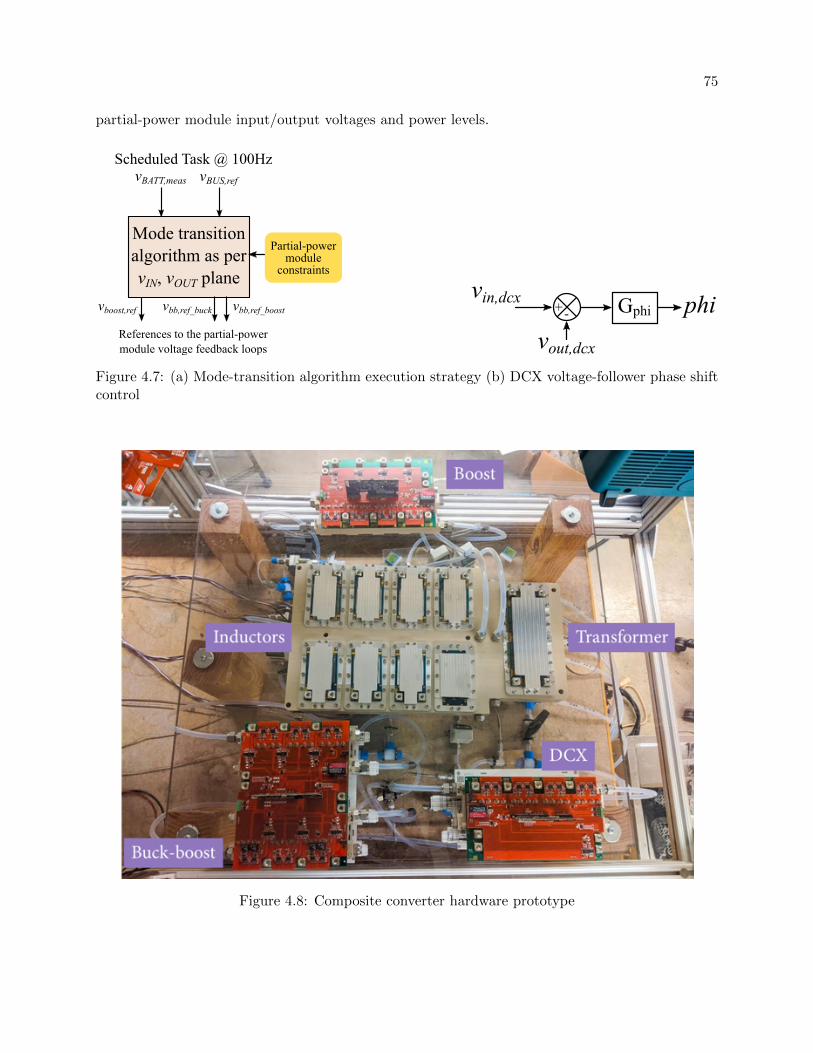
75
partial-power module input/output voltages and power levels.
Figure 4.7: (a) Mode-transition algorithm execution strategy (b) DCX voltage-follower phase shiftcontrol
Figure 4.8: Composite converter hardware prototype
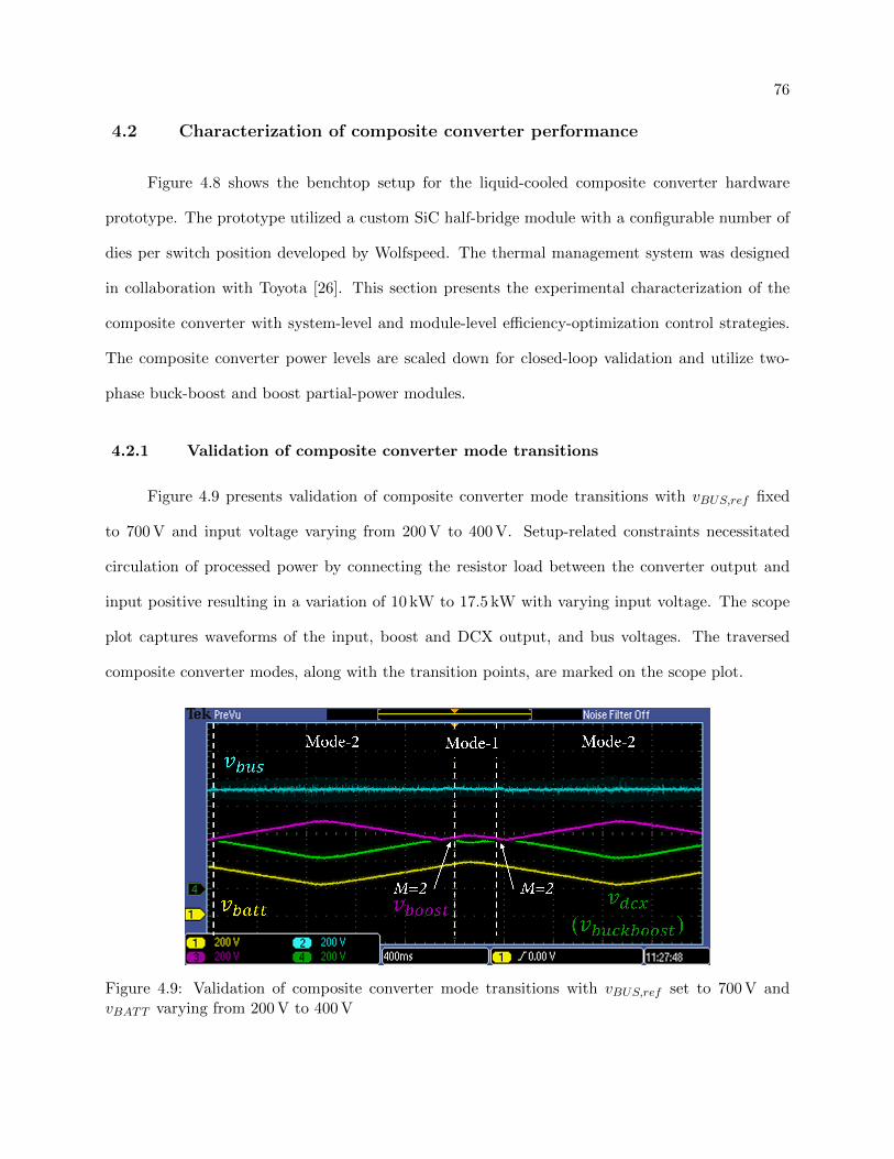
76
4.2 Characterization of composite converter performance
Figure 4.8 shows the benchtop setup for the liquid-cooled composite converter hardware
prototype. The prototype utilized a custom SiC half-bridge module with a configurable number of
dies per switch position developed by Wolfspeed. The thermal management system was designed
in collaboration with Toyota [26]. This section presents the experimental characterization of the
composite converter with system-level and module-level efficiency-optimization control strategies.
The composite converter power levels are scaled down for closed-loop validation and utilize two-
phase buck-boost and boost partial-power modules.
4.2.1 Validation of composite converter mode transitions
Figure 4.9 presents validation of composite converter mode transitions with vBUS,ref fixed
to 700 V and input voltage varying from 200 V to 400 V. Setup-related constraints necessitated
circulation of processed power by connecting the resistor load between the converter output and
input positive resulting in a variation of 10 kW to 17.5 kW with varying input voltage. The scope
plot captures waveforms of the input, boost and DCX output, and bus voltages. The traversed
composite converter modes, along with the transition points, are marked on the scope plot.
Figure 4.9: Validation of composite converter mode transitions with vBUS,ref set to 700 V andvBATT varying from 200 V to 400 V

77
For input voltages between 200 V and 350 V, the composite converter operates in Mode-2
with the buck-boost converter operating in passthrough tracking the input voltage – as observed the
output waveform of the voltage-follower DCX. The boost converter output adjusts its output voltage
in response to the varying input voltage to regulate vBUS to 700 V. The M = 2 passthrough mode
of operation occurs at 350 V input, beyond which the converter transitions to Mode-1 operation.
Boost transitions to passthrough mode with the buck-boost operating in buck-mode to maintain
the vBUS . The waveforms indicate smooth mode transitions with steady regulation of the output
bus in all modes, including transition points.
4.2.2 Efficiency characterization with variation in input voltage for different output
voltages
Figure 4.10 plots the measured composite converter efficiencies for operation with a fixed out-
put current of 25 A at different bus voltages with varying input voltages. The measured efficiencies
are overlayed on the theoretical vBUS/vIN conversion ratio plane and characterize the composite
converter efficiencies across all modes of operation.
The measured efficiencies increase along the positive x-axis with reducing conversion ratios
and decrease along the positive y-axis with increasing conversion ratios. The only exception is the
operation on M = 2 composite-passthrough line, where efficiencies are maximum for a given output
vBUS voltage. The efficiency measured at the 350 V to 700 V passthrough operation is slightly higher
than that measured at a smaller conversion ratio operating point of 400 V to 700 V, which requires
a switching operation of the buck-boost module. Overall, the composite converter operates with
high efficiency across the entire operating range. The minimum and maximum measured efficiency
results are summarized below:
• 98.0% efficiency in mode-3 with input/ output voltages at 250 V and 900 V (M = 3.6) at
24 kW.
• 99% efficiency in the boost-only mode with input/output voltages of 400 V and 600 V
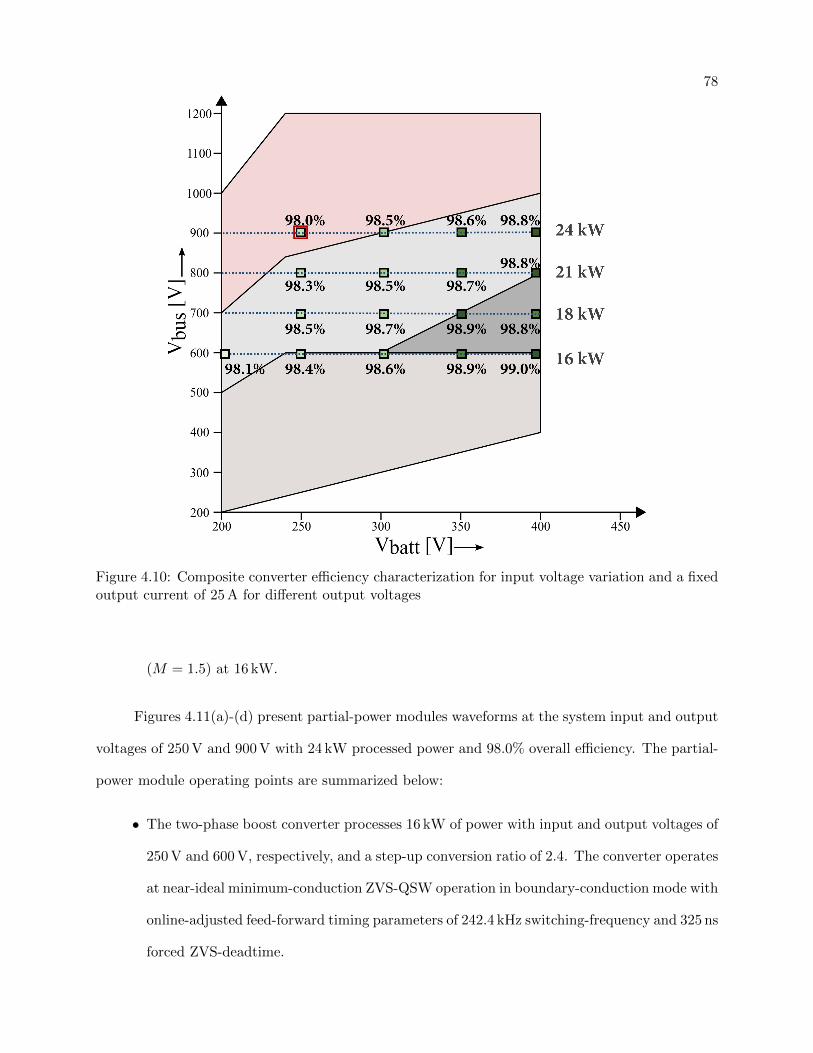
78
Figure 4.10: Composite converter efficiency characterization for input voltage variation and a fixedoutput current of 25 A for different output voltages
(M = 1.5) at 16 kW.
Figures 4.11(a)-(d) present partial-power modules waveforms at the system input and output
voltages of 250 V and 900 V with 24 kW processed power and 98.0% overall efficiency. The partial-
power module operating points are summarized below:
• The two-phase boost converter processes 16 kW of power with input and output voltages of
250 V and 600 V, respectively, and a step-up conversion ratio of 2.4. The converter operates
at near-ideal minimum-conduction ZVS-QSW operation in boundary-conduction mode with
online-adjusted feed-forward timing parameters of 242.4 kHz switching-frequency and 325 ns
forced ZVS-deadtime.
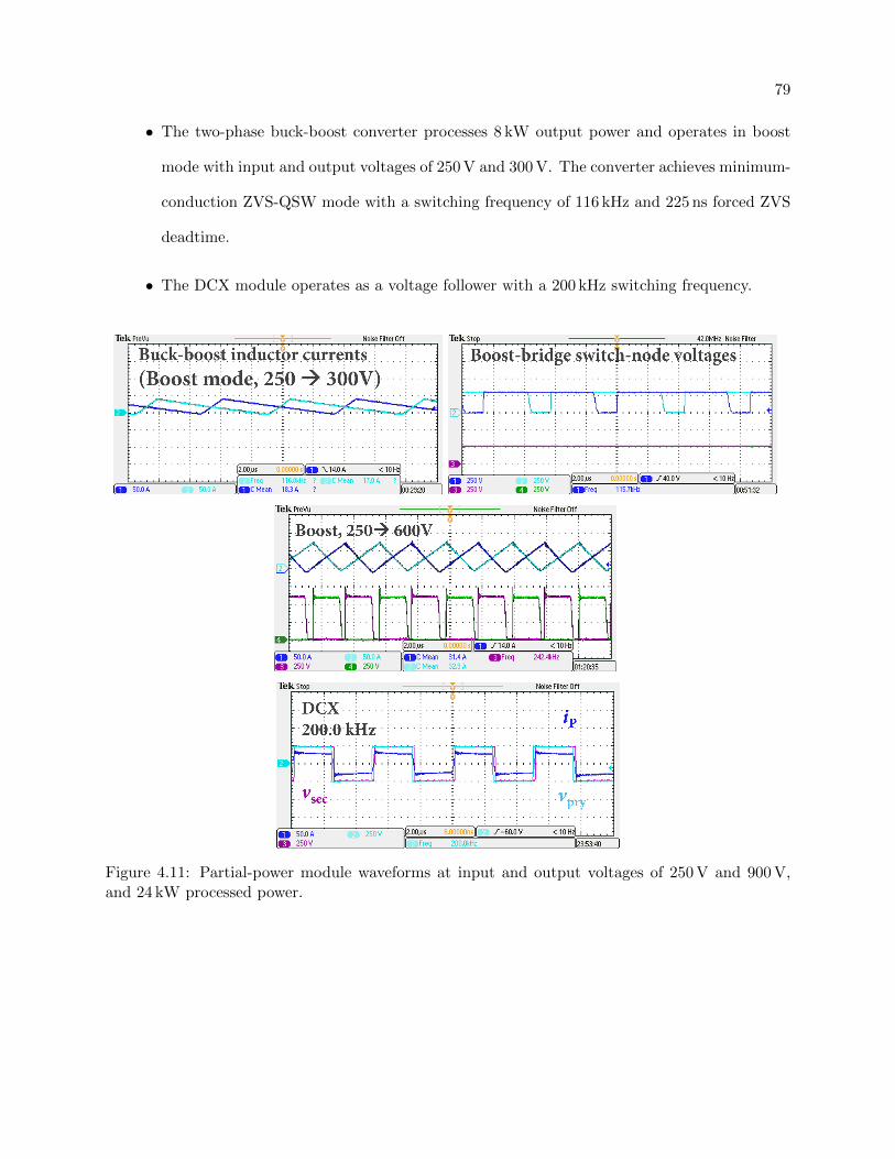
79
• The two-phase buck-boost converter processes 8 kW output power and operates in boost
mode with input and output voltages of 250 V and 300 V. The converter achieves minimum-
conduction ZVS-QSW mode with a switching frequency of 116 kHz and 225 ns forced ZVS
deadtime.
• The DCX module operates as a voltage follower with a 200 kHz switching frequency.
Figure 4.11: Partial-power module waveforms at input and output voltages of 250 V and 900 V,and 24 kW processed power.

80
4.2.3 Efficiency characterization with variation in output power for different output
voltages
Figure 4.12 plots the measured composite converter efficiencies for operation for variation in
processed power with a fixed input voltage of 350 V for different bus voltages. The curves present
composite converter efficiencies with varying power in different modes. With variation in power
levels and operating points, the number of interleaved phases for the boost and the buck-boost
modules are adjusted per the frequency-based phase-shedding strategy.
Figure 4.12: Composite converter efficiency characterization for output power variation with a fixedinput voltage of 350 V at different output voltages
The 600 V Mode-0 efficiency plot effectively plots the efficiency of the multiphase boost
module with additional conduction losses on the DCX rectifier switches. With the module-level
efficiency-optimization strategies presented earlier with frequency-based phase-shedding, the com-
posite converter efficiency remains flat over a wide range in Mode-0. In all other modes that
require DCX voltage-follower operation, the efficiency is relatively low at lower power levels due to
hard-switched operation in the DCX module. The efficiencies peak as the DCX module achieves
optimal-ZVS at specific power levels for corresponding operating voltages. Further increases in
power levels cause dips in system efficiencies due to increased conduction losses attributed to the
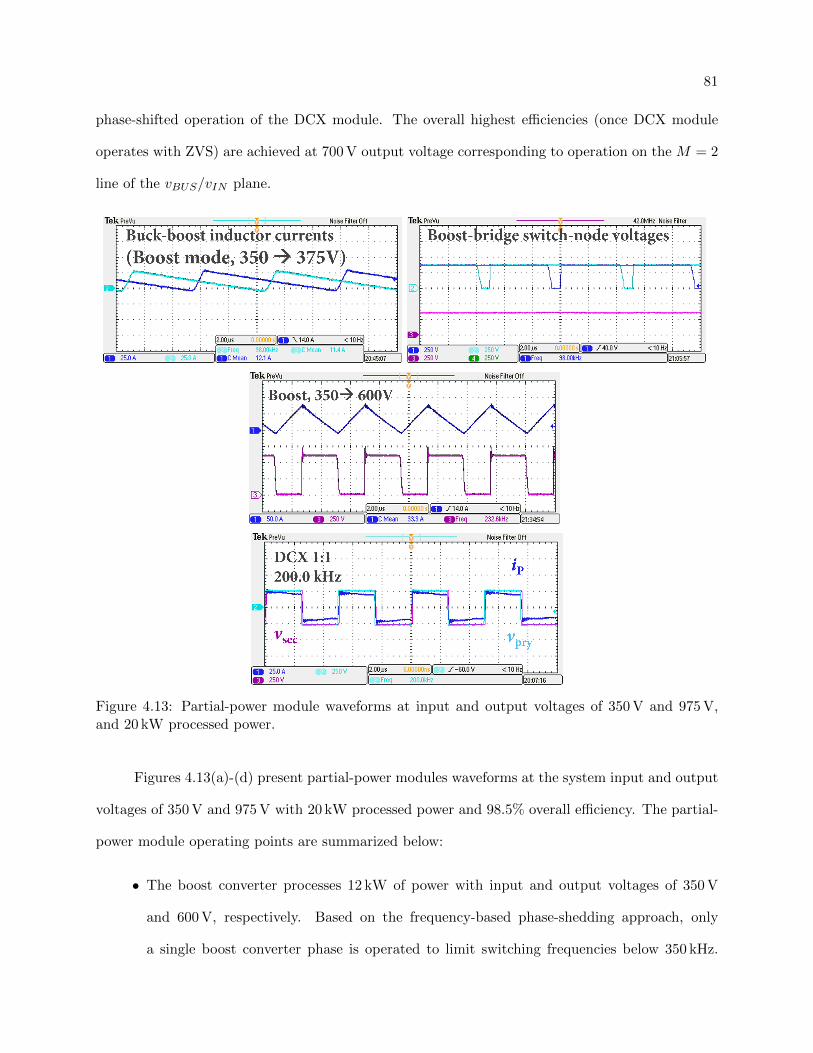
81
phase-shifted operation of the DCX module. The overall highest efficiencies (once DCX module
operates with ZVS) are achieved at 700 V output voltage corresponding to operation on the M = 2
line of the vBUS/vIN plane.
Figure 4.13: Partial-power module waveforms at input and output voltages of 350 V and 975 V,and 20 kW processed power.
Figures 4.13(a)-(d) present partial-power modules waveforms at the system input and output
voltages of 350 V and 975 V with 20 kW processed power and 98.5% overall efficiency. The partial-
power module operating points are summarized below:
• The boost converter processes 12 kW of power with input and output voltages of 350 V
and 600 V, respectively. Based on the frequency-based phase-shedding approach, only
a single boost converter phase is operated to limit switching frequencies below 350 kHz.

82
The converter realizes near-ideal minimum-conduction ZVS-QSW operation with 232.6 kHz
switching-frequency, and 330 ns forced ZVS-deadtime.
• The two-phase buck-boost converter processes 7.7 kW output power and operates in boost
mode with input and output voltages of 350 V and 375 V. The converter switching frequency
hits the minimum limit of 100 kHz. Despite partial hard-switching, module efficiencies are
high due to low conversion ratios.
• The DCX module operates as a voltage follower with a 200 kHz switching frequency.
Chapter 5
Conclusions and Future Directions
5.1 Summary of key contributions and results
This work focuses on the development of control strategies for optimizing the efficiency of
composite dc-dc converters. A composite converter architecture employs partial-power modules
that operate with a restricted range of conversion ratios around the VIN = VOUT passthrough point
achieving high efficiencies while processing much of the indirect power efficiently through dual active
bridge (DAB) based near-fixed-ratio “dc transformer” (DCX) converters. The proposed control
strategies enable online efficiency optimization of the composite converter with varying operating
conditions at both the module and the system level. The major contributions of this thesis and
the key results for the module and the system-level efficiency-optimization control strategies are
summarized in the following sections.
5.1.1 Efficiency-optimized control of a half-bridge boost module
An online efficiency-optimization control strategy is developed for a half-bridge boost module,
which dynamically adjusts the converter switching frequency and forced-ZVS dead times in a feed-
forward manner to achieve wide-range minimum-conduction zero-voltage switching, quasi-square-
wave (ZVS-QSW) operation. The feed-forward optimization loop operating in conjunction with
feedback regulation determines the optimal timing parameters through multivariate polynomial
curve fitting of analytical models constructed from state-plane solutions. Considering switch-node
capacitance variations, the analytical models comprehensively capture the optimal timing param-

84
eter trajectories in three-dimensional surfaces. Multivariate curve fitting of these surfaces results
in easily realizable polynomial functions that predict optimal timing parameters as functions of
input voltage, conversion ratio, and average inductor current with a straightforward extension to
bidirectional power flow.
The proposed online-optimization approach results in significant performance improvements
for the hardware prototype over conventional fixed-frequency and dead-time approaches. The
approach results in efficiencies greater than 98.0% for input voltages ranging from 200 V to 400 V,
step-up conversion ratios up to 2.5, and power levels between 2 and 10 kW. Furthermore, efficiencies
greater than 99% are measured over wide power levels for conversion ratios less than 2. Examining
the converter transient response confirms that the feed-forward optimization has no impact on
the closed-loop operation and achieves minimum-conduction ZVS-QSW operation under varying
operating conditions.
5.1.2 Extension of the online efficiency-optimization approach to multiphase con-
verters
Extending the online efficiency-optimization control strategy developed for a single half-
bridge module to multiphase converters requires several modifications to both the feedback and the
feed-forward loops.
• Additional low-bandwidth current-balancing compensators ensure a balanced operation in
variable-frequency multiphase converters by making minor adjustments to the inner phase-
current compensators to equalize the sensed average currents.
• Multiphase non-inverting buck-boost converters with different half-bridge configurations
for the buck and the boost half-bridges require separate analytical models with a distinct
set of curve-fit coefficients for the buck and the boost modes. Consequently, independent
feedback compensators are employed for the two bridges. A small differential component to
the two voltage-compensator references ensures smooth transitions between the buck and

85
boost modes through an intermediate no-switching passthrough mode.
• A frequency-based phase-shedding approach is introduced that limits the maximum switch-
ing frequencies and extends the range of minimum-conduction ZVS-QSW operation in mul-
tiphase converters. The strategy in conjunction with feed-forward optimization results in
optimal-ZVS operation at lower frequencies. It approaches the performance of conventional
power-based phase shedding with fewer phase transitions, thereby mitigating the impact of
temperature-cycling-based failure mechanisms.
The online efficiency-optimization strategies and its multiphase extension are generalized ap-
proaches to improving power converter efficiencies. The systematic approach to developing analyt-
ical models, the resulting curve fitting process, and the feed-forward and feedback implementation
techniques presented in this thesis can be applied to other converter topologies.
5.1.3 System-level efficiency-optimized control
The composite converter topology relies on efficient operating modes that maximize partial-
power module and system efficiencies for a given conversion ratio. In this work, system-level
control strategies are demonstrated for composite converters that employ a decentralized, scalable
control architecture to achieve closed-loop regulation, determine optimal partial-power operating
modes and achieve efficiency-maximizing mode transitions. Combining system-level and module-
level control strategies results in a composite boost converter topology that achieves efficiencies
greater than 98% for:
• 400 V ≤ vBUS ≤ 900 V
• 250 V ≤ vBATT ≤ 400 V
• 10 kW ≤ pOUT ≤ 30 kW
Furthermore, efficiencies close to 99% are measured for composite conversion ratio of 2 over
wide power ranges. Module and system-level efficiency-optimization control strategies enable design
86
of a composite boost converter prototype that achieves a corporate average fuel economy (CAFE)
efficiency of 99.0% and a power density of 22.4 kW/L.
5.2 Possible directions for further research
A number of possible research and development directions are possible based on the work
presented in this thesis:
• Efficiency-optimized control of the DAB-based DCX module: The module-level
efficiency optimization strategies in this work are focused on the multiphase boost and buck-
boost modules. The dual active bridge DCX module is operated at a fixed frequency as a
voltage follower to the buck-boost module output. As seen from system-level composite-
converter efficiency characterization - both low-power and high-power operating points
are impacted by the DCX performance. Feed-forward optimization of the DAB timing
parameters, sophisticated modulation techniques, and modifications to the DAB circuit
could further improve the system efficiencies.
• Additional composite-converter modes: In this work, the optimal composite con-
verter modes are determined solely from the converter input and output voltages. The
introduction of additional composite converter modes, dependent on input/output voltages
and processed power, resulting in a three-dimensional mode-transition chart, could offer
further performance improvements.
• Bidirectional power-flow/regenerative braking: While the module-level control strate-
gies are bidirectional, the composite converter with its associated system-level control
strategies is not fully characterized under reverse power flow. With an input series, out-
put parallel configuration of the composite boost topology under reverse power flow, a
bidirectional closed-loop operation would require additional balancing considerations and
modifications to the system and module-level control loops.

Bibliography
[1] MIL-217 (1991) Military Handbook: Reliability Prediction of Electronic Equipment. Depart-ment of Defense, Washington DC, USA, 1991.
[2] Jaber A. Abu-Qahouq. Analysis and design of n-phase current-sharing autotuning controller.IEEE Transactions on Power Electronics, 25(6):1641–1651, Jun 2010.
[3] Jaber A. Abu Qahouq, Lilly Huang, and Douglas Huard. Sensorless current sharinganalysis and scheme for multiphase converters. IEEE Transactions on Power Electronics,23(5):2237–2247, Sep 2008.
[4] B. Agrawal, L. Zhou, A. Emadi, and M. Preindl. Variable-frequency critical soft-switchingof wide-bandgap devices for efficient high-frequency nonisolated DC-DC converters. IEEETransactions on Vehicular Technology, 69(6):6094–6106, June 2020.
[5] W. Al-Hoor, J. A. Abu-Qahouq, L. Huang, W. B. Mikhael, and I. Batarseh. Adaptive digitalcontroller and design considerations for a variable switching frequency voltage regulator. IEEETransactions on Power Electronics, 24(11):2589–2602, November 2009.
[6] T.T. Anandha Ruban, Preetam Tadeparthy, Sankaran Aniruddhan, Vikram Gakhar, andMuthusubramanian Venkateswaran. Optimal dynamic phase add/drop mechanism in mul-tiphase dc-dc buck converters. In 2016 IEEE Applied Power Electronics Conference andExposition (APEC), page 1878–1881, Mar 2016.
[7] P. Andreassen and T.M. Undeland. Digital control techniques for current mode control ofinterleaved quasi square wave converter. In 2005 IEEE 36th Power Electronics SpecialistsConference, page 910–914, Jun 2005.
[8] Pal Andreassen, Giuseppe Guidi, and Tore M. Undeland. Digital variable frequency controlfor zero voltage switching and interleaving of synchronous buck converters. In 2006 12thInternational Power Electronics and Motion Control Conference, page 184–188, Aug 2006.
[9] A. Anthon, J. C. Hernandez, Z. Zhang, and M. A. E. Andersen. Switching investigations on aSiC MOSFET in a TO-247 package. In IECON 2014 - 40th Annual Conference of the IEEEIndustrial Electronics Society, pages 1854–1860, October 2014. ISSN: 1553-572X.
[10] J. Baek, W. Choi, and B. Cho. Digital adaptive frequency modulation for bidirectional DC–DCconverter. IEEE Transactions on Industrial Electronics, 60(11):5167–5176, November 2013.

88
[11] J. Baek, W. Choi, and B. Cho. Digital adaptive frequency modulation for bidirectional dc–dcconverter. IEEE Transactions on Industrial Electronics, 60(11):5167–5176, Nov 2013.
[12] Berker Bilgin, Pierre Magne, Pawel Malysz, Yinye Yang, Vera Pantelic, Matthias Preindl,Alexandre Korobkine, Weisheng Jiang, Mark Lawford, and Ali Emadi. Making the case forelectrified transportation. IEEE Transactions on Transportation Electrification, 1(1):4–17, Jun2015.
[13] Tania C. Cano, Ignacio Castro, Alberto Rodrıguez, Diego G. Lamar, Yehia F. Khalil, LauraAlbiol-Tendillo, and Parag Kshirsagar. Future of electrical aircraft energy power systems: Anarchitecture review. IEEE Transactions on Transportation Electrification, 7(3):1915–1929, Sep2021.
[14] F. Caricchi, F. Crescimbini, and A. Di Napoli. 20 kw water-cooled prototype of a buck-boostbidirectional dc-dc converter topology for electrical vehicle motor drives. In Proceedings of1995 IEEE Applied Power Electronics Conference and Exposition - APEC’95, volume 2, page887–892 vol.2, Mar 1995.
[15] H. Chen, H. Kim, R. Erickson, and D. Maksimovic. Electrified automotive powertrain architec-ture using composite DC–DC converters. IEEE Transactions on Power Electronics, 32(1):98–116, January 2017.
[16] H. Chen, K. Sabi, H. Kim, T. Harada, R. Erickson, and D. Maksimovic. A 98.7% effi-cient composite converter architecture with application-tailored efficiency characteristic. IEEETransactions on Power Electronics, 31(1):101–110, January 2016.
[17] Jianjun Chen, Xi Jiang, Zongjian Li, Hengyu Yu, Jun Wang, and Z. John Shen. Investigationon effects of thermal stress on sic mosfet degradation through power cycling tests. In 2020IEEE Applied Power Electronics Conference and Exposition (APEC), page 1106–1110, Mar2020.
[18] Jingquan Chen, D. Maksimovic, and R. Erickson. Buck-boost pwm converters having twoindependently controlled switches. In 2001 IEEE 32nd Annual Power Electronics SpecialistsConference (IEEE Cat. No.01CH37230), volume 2, page 736–741 vol.2, Jun 2001.
[19] Ying-Chi Chen, Jhih-Da Hsu, Yong-Ann Ang, and Ta-Yung Yang. A new phase sheddingscheme for improved transient behavior of interleaved boost pfc converters. In 2014 IEEEApplied Power Electronics Conference and Exposition - APEC 2014, page 1916–1919, Mar2014.
[20] Xu-Feng Cheng, Chenyang Liu, Dianlong Wang, and Yong Zhang. State-of-the-art review onsoft-switching technologies for non-isolated dc-dc converters. IEEE Access, 9:119235–119249,2021.
[21] Shamar Christian, Roberto A. Fantino, Roderick A. Gomez, Yue Zhao, and Juan C. Balda.High power density interleaved ZCS 80-kW boost converter for automotive applications. IEEEJournal of Emerging and Selected Topics in Power Electronics, pages 1–1, 2021.
[22] L. Corradini, D. Maksimovic, P Mattavelli, and R. Zane. Digital Control of High-FrequencySwitched-Mode Power Converters. Wiley-IEEE Press, 2015.
89
[23] A. Costabeber, P. Mattavelli, and S. Saggini. Digital time-optimal phase shedding in multi-phase buck converters. IEEE Transactions on Power Electronics, 25(9):2242–2247, Sep 2010.
[24] D. Costinett, D. Maksimovic, and R. Zane. Circuit-oriented treatment of nonlinear capaci-tances in switched-mode power supplies. IEEE Transactions on Power Electronics, 30(2):985–995, February 2015.
[25] Daniel Costinett, Dragan Maksimovic, and Regan Zane. Design and control for high efficiencyin high step-down dual active bridge converters operating at high switching frequency. IEEETransactions on Power Electronics, 28(8):3931–3940, Aug 2013.
[26] Ercan M. Dede, Yucheng Gao, Yuqing Zhou, Vivek Sankaranarayanan, Feng Zhou, DraganMaksimovic, and Robert W. Erickson. Thermal design, optimization, and packaging of planarmagnetic components. IEEE Transactions on Components, Packaging and ManufacturingTechnology, 11(9):1480–1488, Sep 2021.
[27] Gabriel Eirea and Seth R. Sanders. Phase current unbalance estimation in multiphase buckconverters. IEEE Transactions on Power Electronics, 23(1):137–143, Jan 2008.
[28] John Elmes, Rene Kersten, Issa Batarseh, Michael Pepper, and Keith Mansfield. Modularbidirectional dc-dc converter for hybrid/electric vehicles with variable-frequency interleavedsoft-switching. In 2009 IEEE Vehicle Power and Propulsion Conference, page 448–454, Sep2009.
[29] R. Erickson and D. Maksimovic. Fundamentals of Power Electronics. Springer, Cham, 2020.
[30] Roberto Fantino, Shamar Christian, and Juan C. Balda. Synchronous-variable-frequency con-trol of bidirectional dcm interleaved dc-dc converter for wide-range enhanced efficiency. IEEETransactions on Industrial Electronics, page 1–1, 2021.
[31] Minfan Fu, Chao Fei, Yuchen Yang, Qiang Li, and Fred C. Lee. Optimal design of planarmagnetic components for a two-stage gan-based dc–dc converter. IEEE Transactions on PowerElectronics, 34(4):3329–3338, Apr 2019.
[32] Y. Gao, V. Sankaranarayanan, E. M. Dede, A. Ghosh, D. Maksimovic, and R. W. Erickson.Drive-cycle optimized 99% efficient SiC boost converter using planar inductor with enhancedthermal management. In 2019 20th Workshop on Control and Modeling for Power Electronics(COMPEL), pages 1–7, June 2019.
[33] Y. Gao, V. Sankaranarayanan, E. M. Dede, A. Ghosh, D. Maksimovic, and R. W. Erick-son. Drive-cycle optimized 99% efficient SiC boost converter using planar inductor with en-hanced thermal management. In Proc. IEEE 20th Workshop Control Model. Power Electron.(COMPEL), pages 1–7, 2019.
[34] Yucheng Gao. Design and Optimization of a 100-kW Composite Converter for Electric VehicleDrivetrain. PhD thesis, University of Colorado at Boulder, 2021.
[35] Yucheng Gao, Vivek Sankaranarayanan, Robert W. Erickson, and Dragan Maksimovic. Softstartup strategies for dab-based dcx in composite converters. In 2020 IEEE Energy ConversionCongress and Exposition (ECCE), page 6130–6135, Oct 2020.
90
[36] C. P. Henze, H. C. Martin, and D. W. Parsley. Zero-voltage switching in high frequency powerconverters using pulse width modulation. In APEC ’88 Third Annual IEEE Applied PowerElectronics Conference and Exposition, pages 33–40, February 1988.
[37] Juan C. Hernandez, Maria C. Mira, Lars P. Petersen, Michael A. E. Andersen, and Niels H. Pe-tersen. Zero voltage switching control method for mhz boundary conduction mode converters.IEEE Transactions on Industrial Electronics, 67(2):1544–1554, Feb 2020.
[38] Ping-Ching Huang, Wei-Quan Wu, Hsin-Hsin Ho, and Ke-Horng Chen. Hybrid buck–boostfeedforward and reduced average inductor current techniques in fast line transient and high-efficiency buck–boost converter. IEEE Transactions on Power Electronics, 25(3):719–730, Mar2010.
[39] Q. Huang and A. Q. Huang. Variable frequency average current mode control for ZVS sym-metrical dual-buck H-bridge All-GaN inverter. IEEE Journal of Emerging and Selected Topicsin Power Electronics, 8(4):4416–4427, December 2020.
[40] Q. Huang, R. Yu, Q. Ma, and A. Q. Huang. Predictive ZVS control with improved ZVStime margin and limited variable frequency range for a 99% efficient, 130-W/in3 MHz GaNtotem-pole PFC rectifier. IEEE Transactions on Power Electronics, 34(7):7079–7091, July2019.
[41] Laszlo Huber, Brian T. Irving, and Milan M. Jovanovic. Open-loop control methods forinterleaved dcm/ccm boundary boost pfc converters. IEEE Transactions on Power Electronics,23(4):1649–1657, Jul 2008.
[42] IXYS Integrated Circuits Division. Reliability report: AEC-Q100-REV Automo-tive Qualification for IXDD604SI, IXDF604SI, IXDI604SI, IXDN604SI. Available:https://www.ixysic.com/Index/QualityReports/CodeV2A1.pdf, May 2012.
[43] E. A. Jones, F. F. Wang, and D. Costinett. Review of commercial GaN power devices andGaN-based converter design challenges. IEEE Journal of Emerging and Selected Topics inPower Electronics, 4(3):707–719, September 2016.
[44] S. H. Kang, D. Maksimovic, and I. Cohen. Efficiency optimization in digitally controlledflyback DC–DC converters over wide ranges of operating conditions. IEEE Transactions onPower Electronics, 27(8):3734–3748, August 2012.
[45] Matthias Kasper, Ralph M. Burkart, Gerald Deboy, and Johann W. Kolar. ZVS of powerMOSFETs revisited. IEEE Transactions on Power Electronics, 31(12):8063–8067, December2016.
[46] A. Kelly. Current share in multiphase dc–dc converters using digital filtering techniques. IEEETransactions on Power Electronics, 24(1):212–220, Jan 2009.
[47] Hyeokjin Kim, Hua Chen, Dragan Maksimovic, Robert Erickson, Zach Cole, Brandon Pass-more, and Kraig Olejniczak. Sic-mosfet composite boost converter with 22 kw/l power densityfor electric vehicle application. In 2017 IEEE Applied Power Electronics Conference andExposition (APEC), page 134–141, Mar 2017.
91
[48] J. W. Kolar, J. Biela, and J. Minibock. Exploring the pareto front of multi-objective single-phase PFC rectifier design optimization - 99.2% efficiency vs. 7kW/din3 power density. In2009 IEEE 6th International Power Electronics and Motion Control Conference, pages 1–21,May 2009.
[49] T. Konjedic, L. Korosec, M. Truntic, C. Restrepo, M. Rodic, and M. Milanovic. DCM-basedzero-voltage switching control of a bidirectional DC–DC converter with variable switchingfrequency. IEEE Transactions on Power Electronics, 31(4):3273–3288, April 2016.
[50] Florian Krismer and Johann W. Kolar. Accurate small-signal model for the digital controlof an automotive bidirectional dual active bridge. IEEE Transactions on Power Electronics,24(12):2756–2768, Dec 2009.
[51] Hoai Nam Le and Jun-Ichi Itoh. Wide-load-range efficiency improvement for high-frequencysic-based boost converter with hybrid discontinuous current mode. IEEE Transactions onPower Electronics, 33(2):1843–1854, 2018.
[52] Young-Joo Lee, Alireza Khaligh, and Ali Emadi. A compensation technique for smooth tran-sitions in a noninverting buck–boost converter. IEEE Transactions on Power Electronics,24(4):1002–1015, Apr 2009.
[53] X. Li, X. Li, P. Liu, S. Guo, L. Zhang, A. Q. Huang, X. Deng, and B. Zhang. Achievingzero switching loss in silicon carbide MOSFET. IEEE Transactions on Power Electronics,34(12):12193–12199, December 2019.
[54] Bo Liu, Ren Ren, Zheyu Zhang, Ben Guo, Fei Wang, and Daniel Costinett. Impacts of highfrequency, high di/dt, dv/dt environment on sensing quality of gan based converters and theirmitigation. CPSS Transactions on Power Electronics and Applications, 3(4):301–312, Dec2018.
[55] Y.-C. Liu, Y.-L. Syu, N. A. Dung, C. Chen, K.-D. Chen, and K. A. Kim. High-switching-frequency TCM digital control for bidirectional-interleaved buck converters without phase errorfor battery charging. IEEE Journal of Emerging and Selected Topics in Power Electronics,8(3):2111–2123, September 2020.
[56] Yu-Chen Liu, Yong-Long Syu, Nguyen Anh Dung, Chen Chen, Kai-De Chen, and Katherine A.Kim. High-switching-frequency tcm digital control for bidirectional-interleaved buck converterswithout phase error for battery charging. IEEE Journal of Emerging and Selected Topics inPower Electronics, 8(3):2111–2123, Sep 2020.
[57] Zhengyang Liu, Zhengrong Huang, Fred C. Lee, and Qiang Li. Digital-based interleavingcontrol for gan-based mhz crm totem-pole pfc. IEEE Journal of Emerging and Selected Topicsin Power Electronics, 4(3):808–814, Sep 2016.
[58] Zhengyang Liu, Fred C. Lee, Qiang Li, and Yuchen Yang. Design of gan-based mhz totem-polepfc rectifier. IEEE Journal of Emerging and Selected Topics in Power Electronics, 4(3):799–807,Sep 2016.
[59] D. Lyu, G. Shi, R. Min, Q. Tong, Q. Zhang, L. Li, and G. Shen. Extended off-time controlfor CRM boost converter based on piecewise equivalent capacitance model. IEEE Access,8:155891–155901, 2020.
92
[60] D. Maksimovic. Design of the zero-voltage-switching quasi-square-wave resonant switch. InProceedings of IEEE Power Electronics Specialist Conference - PESC ’93, pages 323–329, June1993.
[61] C. Marxgut, F. Krismer, D. Bortis, and J. W. Kolar. Ultraflat interleaved triangular currentmode (TCM) single-phase PFC rectifier. IEEE Transactions on Power Electronics, 29(2):873–882, February 2014.
[62] The MathWorks, Inc., Natick, MA. Curve Fitting Toolbox User’s Guide, 2020b. Version3.5.12.
[63] D. Neumayr, D. Bortis, E. Hatipoglu, J. W. Kolar, and G. Deboy. Novel efficiency-optimalfrequency modulation for high power density DC/AC converter systems. In 2017 IEEE 3rdInternational Future Energy Electronics Conference and ECCE Asia (IFEEC 2017 - ECCEAsia), pages 834–839, June 2017.
[64] K. D. T. Ngo. Generalization of resonant switches and quasi-resonant DC-DC converters.In 1987 IEEE Power Electronics Specialists Conference, pages 395–403, June 1987. ISSN:0275-9306.
[65] Hoang Vu Nguyen, Dong-Choon Lee, and Frede Blaabjerg. A novel sic-based multifunctionalonboard battery charger for plug-in electric vehicles. IEEE Transactions on Power Electronics,36(5):5635–5646, May 2021.
[66] Ziwei Ouyang and Michael A. E. Andersen. Overview of planar magnetic technol-ogy—fundamental properties. IEEE Transactions on Power Electronics, 29(9):4888–4900, Sep2014.
[67] Y. Panov and M. M. Jovanovic. Adaptive off-time control for variable-frequency, soft-switchedflyback converter at light loads. IEEE Transactions on Power Electronics, 17(4):596–603, July2002.
[68] Martin Pavlovsky, Giuseppe Guidi, and Atsuo Kawamura. Assessment of coupled and in-dependent phase designs of interleaved multiphase buck/boost dc–dc converter for ev powertrain. IEEE Transactions on Power Electronics, 29(6):2693–2704, 2014.
[69] Yang Qiu, Ming Xu, Kaiwei Yao, Juanjuan Sun, and F.C. Lee. The multi-frequency small-signal model for buck and multiphase interleaving buck converters. In Twentieth Annual IEEEApplied Power Electronics Conference and Exposition, 2005. APEC 2005., volume 1, pages392–398 Vol. 1, Mar 2005.
[70] C. Quinn, K. Rinne, T. O’Donnell, M. Duffy, and C.O. Mathuna. A review of planar magnetictechniques and technologies. In APEC 2001. Sixteenth Annual IEEE Applied Power ElectronicsConference and Exposition (Cat. No.01CH37181), volume 2, page 1175–1183 vol.2, Mar 2001.
[71] X. Ren, Y. Wu, Z. Guo, Z. Zhang, and Q. Chen. An online monitoring method of circuitparameters for variable on-time control in RM boost PFC converters. IEEE Transactions onPower Electronics, 34(2):1786–1797, February 2019.
[72] A. Rodriguez, A. Vazquez, M. R. Rogina, and F. Briz. Synchronous boost converter with highefficiency at light load using QSW-ZVS and SiC mosfets. IEEE Transactions on IndustrialElectronics, 65(1):386–393, January 2018.

93
[73] Maria R. Rogina, Alberto Rodriguez, Aitor Vazquez, and Diego G. Lamar. Improving theefficiency of sic-based synchronous boost converter under variable switching frequency tcm anddifferent input/output voltage ratios. IEEE Transactions on Industry Applications, 55(6):7757–7764, 2019.
[74] V. Sankaranarayanan, Y. Gao, R. W. Erickson, and D. Maksimovic. Online efficiency opti-mization of a closed-loop controlled sic-based boost converter. In 2020 IEEE Applied PowerElectronics Conference and Exposition (APEC), pages 285–291, 2020.
[75] Suyash Sushilkumar Shah and Subhashish Bhattacharya. Reliability oriented design of dualactive bridge converter for power supply on heavy-vehicles. In 2018 IEEE Energy ConversionCongress and Exposition (ECCE), page 4102–4109, Sep 2018.
[76] D. Shahzad, S. Pervaiz, N. Zaffar, and K. K. Afridi. Control of a gan-based high-power-density single-phase online uninterruptible power supply. In 2019 20th Workshop on Controland Modeling for Power Electronics (COMPEL), pages 1–6, 2019.
[77] Yanjun Shi, Yu Zhang, Lu Wang, and Hui Li. Reduction of emi noise due to nonideal inter-leaving in a 100 kw sic pv converter. IEEE Transactions on Power Electronics, 34(1):13–19,Jan 2019.
[78] Skyworks. Isolated Amplifier for Current Shunt Measurement, 2021.
[79] Alex Smith. Design considerations for isolated current sensing. Application Brief (SLYT810),2021.
[80] Jen-Ta Su and Chih-Wen Liu. A novel phase-shedding control scheme for improved light loadefficiency of multiphase interleaved dc–dc converters. IEEE Transactions on Power Electronics,28(10):4742–4752, Oct 2013.
[81] Juanjuan Sun, Yang Qiu, Ming Xu, and F.C. Lee. Dynamic current sharing analyses formultiphase buck vrs. In Twenty-First Annual IEEE Applied Power Electronics Conferenceand Exposition, 2006. APEC ’06., pages 7 pp.–, Mar 2006.
[82] Texas Instruments. TMS320F2837xD Dual-Core Microcontrollers, 2019.
[83] Aitor Vazquez, Kevin Martin, Manuel Arias, and Javier Sebastian. Variable-width hystereticanalog control for qsw-zvs and tcm source/sink converters. IEEE Transactions on PowerElectronics, 35(3):3195–3207, Mar 2020.
[84] Aitor Vazquez, Alberto Rodriguez, Diego G. Lamar, and Marta M. Hernando. Advancedcontrol techniques to improve the efficiency of ipop modular qsw-zvs converters. IEEETransactions on Power Electronics, 33(1):73–86, Jan 2018.
[85] Stefan Waffler and Johann W. Kolar. A novel low-loss modulation strategy for high-power bidi-rectional buck + boost converters. IEEE Transactions on Power Electronics, 24(6):1589–1599,Jun 2009.
[86] Baocheng Wang, Ye Yuan, Yang Zhou, and Xiaofeng Sun. Buck/boost bidirectional convertertcm control without zero-crossing detection. In 2016 IEEE 8th International Power Electronicsand Motion Control Conference (IPEMC-ECCE Asia), page 3073–3078, May 2016.
94
[87] K. Wang, H. Zhu, J. Wu, X. Yang, and L. Wang. Adaptive driving scheme for ZVS and mini-mizing circulating current in MHz CRM converters. IEEE Transactions on Power Electronics,36(4):3633–3637, April 2021.
[88] Zhigang Yao and Shuai Lu. A simple approach to enhance the effectiveness of passive currentsbalancing in an interleaved multiphase bidirectional dc–dc converter. IEEE Transactions onPower Electronics, 34(8):7242–7255, Aug 2019.
[89] V. Yousefzadeh and D. Maksimovic. Sensorless optimization of dead times in dc–dc converterswith synchronous rectifiers. IEEE Transactions on Power Electronics, 21(4):994–1002, July2006.
[90] Jingrong Yu, Maoyun Liu, Dongran Song, Jian Yang, and Mei Su. A soft-switching control forcascaded buck-boost converters without zero-crossing detection. IEEE Access, 7:32522–32536,2019.
[91] Zhe Yu, Holger Kapels, and Klaus F. Hoffmann. High efficiency bidirectional dc-dc con-verter with wide input and output voltage ranges for battery systems. In Proceedings ofPCIM Europe 2015; International Exhibition and Conference for Power Electronics, IntelligentMotion, Renewable Energy and Energy Management, page 1–8, May 2015.
[92] Zhe Yu, Holger Kapels, and Klaus F. Hoffmann. Extreme high efficiency non-inverting buck-boost converter for energy storage systems. In PCIM Europe 2016; International Exhibitionand Conference for Power Electronics, Intelligent Motion, Renewable Energy and EnergyManagement, page 1–8, May 2016.
[93] Zhe Yu, Holger Kapels, and Klaus F. Hoffmann. A novel control concept for high-efficiencypower conversion with the bidirectional non-inverting buck-boost converter. In 2016 18thEuropean Conference on Power Electronics and Applications (EPE’16 ECCE Europe), page1–10, Sep 2016.
[94] M.T. Zhang, M.M. Jovanovic, and F.C.Y. Lee. Analysis and evaluation of interleaving tech-niques in forward converters. IEEE Transactions on Power Electronics, 13(4):690–698, Jul1998.
[95] Y. Zhang, C. Chen, T. Liu, K. Xu, Y. Kang, and H. Peng. A high efficiency model-basedadaptive dead-time control method for GaN HEMTs considering nonlinear junction capacitorsin triangular current mode Operation. IEEE Journal of Emerging and Selected Topics in PowerElectronics, 8(1):124–140, March 2020.
[96] Z. Zhang, H. Lu, D. J. Costinett, F. Wang, L. M. Tolbert, and B. J. Blalock. Model-baseddead time optimization for voltage-source converters utilizing silicon carbide semiconductors.IEEE Transactions on Power Electronics, 32(11):8833–8844, November 2017.
[97] Zongjie Zhou, Haiyan Li, and Xinke Wu. A constant frequency zvs control system for thefour-switch buck–boost dc–dc converter with reduced inductor current. IEEE Transactions onPower Electronics, 34(7):5996–6003, Jul 2019.
[98] P. Zumel, C. Fernandez, A. de Castro, and O. Garcıa. Efficiency improvement in multiphaseconverter by changing dynamically the number of phases. In 2006 37th IEEE Power ElectronicsSpecialists Conference, page 1–6, Jun 2006.

Appendix A
Analytical Models for Minimum-conduction ZVS-QSW Operation
This section presents a step-by-step approach in MATLAB® to developing the analytical
models for minimum-conduction ZVS-QSW optimal timing parameters over the converter’s full
range of operation. The optimal timing parameters in the analytical models are obtained by
numerically solving the minimum-conduction ZVS state-plane equations of the converter subject to
operating point constraints (values of m, equivalent switch-node capacitance, and average inductor
current).
Step 1: Create the input parameter coordinate system
The vectors for input and output voltage, and the average inductor current are set up as
follows:
vin vec = 200, 205, · · · , 400
vout vec = 200, 205, · · · , 600
iL vec = 5, 10, · · · , 50
The input coordinate system (vIN , vOUT , iL,avg) consisting of all combinations of the the
three operating-point variables can be created using the function:
[vIN , vOUT , iL,avg] = meshgrid(vin vec, vout vec, iL vec)

96
Each input variable is stored as a three-dimensional (row, column, page) matrix. The size of
the each dimension is equal to the length of the corresponding vector. As an example, accessing
each of the three matrices with an index (31, 61, 4) results in an operating point with vIN , vOUT ,
and iL,avg equal to 350 V, 500 V and 20 A, respectively. Evaluating conversion ratio m at every
output/input voltage combination transforms the original coordinate system to the (vIN , m, iL,avg)
system.
Step 2: Compute the charge-equivalent switch-node capacitance
For a given output voltage in a boost converter, the charge equivalent switch-node capacitance
Ceq,Q follows from (2.2). The calculation of this capacitance, as detailed in [24], requires extracting
the device capacitance as a function of drain-to-source voltage from the device datasheet, plotting
the equivalent switch-node capacitance curve, and numerically integrating this curve to evaluate
the area under the curve. The charge-equivalent capacitance is computed for each value in the
vout vec. For the devices in the experimental prototype, this capacitance is plotted as a function
of the output voltage in Fig. 2.8(b).
Figure A.1: A state-plane diagram example for m < 2 continuous-conduction mode, with state-plane angles and normalization factors shown.

97
Step 3: Solution using the state-plane
The minimum-conduction ZVS-QSW state-plane requires vIN , vOUT , iL,avg, Ceq,Q, and the
constant inductance value L. The state-plane diagram is solved numerically to obtain the optimal
timing parameters, fsw and tdf . The voltage and current normalization factors, iB and vB, are
shown in the m < 2 state-plane of Fig. A.1 as an example.
The state-plane equations derived in [60] are rearranged in terms of the unknown quantities
jL1, jL2, jL3, jL4, and fsw,opt. The minimum-conduction ZVS requirement reduces the number of
unknown quantities by imposing the mode-dependent constraints:
jL4 = 0, for m < 2
jL4, jL3 = 0, for m = 2
jL3 = 0, for m > 2
The function vpasolve is used to numerically solve the system of equations for the specified
unknown quantities. The unknown quantities in the state plane all lie in the interval [0∞] that may
be specified as a search-range parameter to vpasolve. The numerical solver outputs the normalized
inductor currents and the optimal frequency fsw,opt. The forced-ZVS dead time interval tdf is
obtained by denormalizing the state-plane angle β found from the solutions for jL3 or jL4. For the
boost converter, β is given as:
β =
π2 + atan(m−1
jL3), for m < 2
π, for m = 2
π2 + atan( 1
jL4), for m > 2
An important point to note is that the values of m passed to the solver may vary from 0.5
to 3 since vOUT varies from 200 V to 600 V. Since the state plane diagrams considered here are
valid only for the boost mode of operation with m > 1, a precondition check is implemented before

98
invoking the numerical solver.
Step 4: Trimming the data and plotting the model results
The optimal timing parameters fsw,opt and tdf,opt are evaluated at every point in the coor-
dinate system of the input variables. The invalid operating point (m < 1) solutions are excluded
from the solutions by replacing them with NaN . Points exceeding any other limitations, such as
conversion ratio range, or power limits may be excluded similarly.
The model results are plotted using the surf function. Each surface corresponds to all valid
analytical solutions on a specific page for a particular iL,avg in fsw,opt and tdf,opt matrices. Since all
pages in the tdf,opt matrix are identical, only one needs plotting.
Frequency and dead-time analytical models for the buck-boost converter
The frequency and forced ZVS dead-time analytical models developed using the steps detailed
previously for minimum-conduction ZVS-QSW operation for the buck and boost half-bridges of
the non-inverting buck-boost converter are presented in Figures A.2 and A.3. The buck half-bridge
employs a 1-die per switch position half-bridge module, while the boost bridge utilizes a two-die
per switch position module with both bridges connected to a 7.5 µH inductor. Consequently, the
two-die analytical modules require larger time intervals to achieve minimum-conduction ZVS-QSW
operation over the same operational range. A downward shift in the frequency surfaces and an
upward shift in the dead-time analytical plane is therefore evident in the 2-die models of Fig.A.2
compared to 1-die models of Fig.A.3.
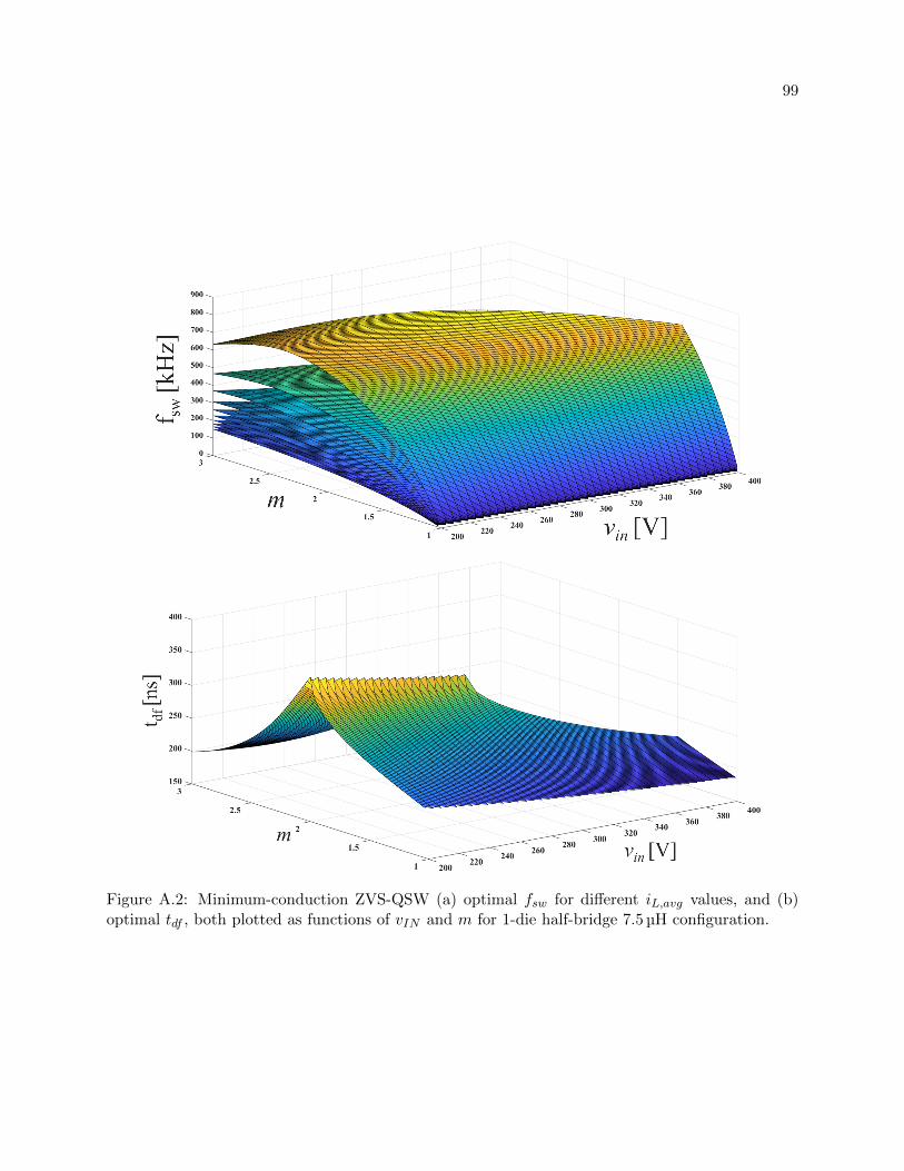
99
Figure A.2: Minimum-conduction ZVS-QSW (a) optimal fsw for different iL,avg values, and (b)optimal tdf , both plotted as functions of vIN and m for 1-die half-bridge 7.5 µH configuration.
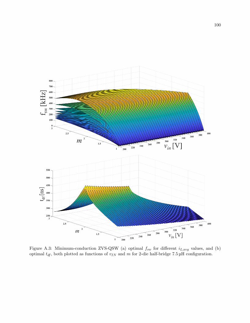
100
Figure A.3: Minimum-conduction ZVS-QSW (a) optimal fsw for different iL,avg values, and (b)optimal tdf , both plotted as functions of vIN and m for 2-die half-bridge 7.5 µH configuration.
Related Documents