ECOLE POLYTECHNIQUE FEDERALE DE LAUSANNE ÉCOLE POLYTECHNIQUE FÉDÉRALE DE LAUSANNE Control And Readout Electronics For DNA Biosensor Arrays by Nicolas Huguenin-Virchaux in the LSM - Microelectronic Systems Laboratory Professor Yusuf Leblebici Supervisor Yuksel Temiz CoSupervisor Sevil Zeynep Temel June 2010

Welcome message from author
This document is posted to help you gain knowledge. Please leave a comment to let me know what you think about it! Share it to your friends and learn new things together.
Transcript

ECOLE POLYTECHNIQUE FEDERALE DE LAUSANNE
ÉCOLE POLYTECHNIQUEFÉDÉRALE DE LAUSANNE
Control And Readout Electronics For
DNA Biosensor Arrays
by
Nicolas Huguenin-Virchaux
in the
LSM - Microelectronic Systems Laboratory
Professor Yusuf Leblebici
Supervisor Yuksel Temiz
CoSupervisor Sevil Zeynep Temel
June 2010

Abstract
by Nicolas Huguenin-Virchaux
The advancement of microelectronics and its application in biochemistry has led to
promising implementations of new biosensors. Instead of bulky external equipment to
excite, amplify and detect an optical signal from a so called passive biosensor, there are
analog and digital microelectronics directly integrated on chip to quantify an electro-
chemical sensor current. These active biosensors open a whole new field of applications
and can be used in mobile environment and point-of-care applications such as diagnos-
tics, health care and biochemistry research. The purpose of this semester project is to
compare different implementations of a microelectronic interface and to implement the
most promising architecture. The schematic and layout will be done using state of the
art Cadence Design automation software for the UMC180 process technology, and the
simulation of the overall system will be discussed.

Acknowledgements
I first would like to thank my adviser, Yuksel Temiz from the Microelectronic Systems
Laboratory, for his continuous support in the semester thesis. He was always there to
listen and give good advice. My thanks also go to Prof. Yusuf Leblebici, director of the
laboratory, and Alain Vachoux for providing me with the necessary EDA design tools and
the working environment at LSM. In addition, I would like to thank Sevil Zeynep Temel
for her hints and explanations concerning the layout. Finally I also would like to thank
my family, especially my parents, for their unconditional support and encouragement to
pursue my interests.
ii
Contents
Abstract i
Acknowledgements ii
List of Figures v
1 Introduction To Electrochemical DNA-Sensing 1
1.1 What Is An Electrochemical Biosensor . . . . . . . . . . . . . . . . . . . . 1
1.2 Potentiostatic Setup For Cyclic Voltammetry . . . . . . . . . . . . . . . . 2
1.3 Electrochemical Reaction . . . . . . . . . . . . . . . . . . . . . . . . . . . 3
2 Comparison Of Different Architectures 5
2.1 Dual Slope ADC (fixed time integration)[1]: . . . . . . . . . . . . . . . . . 5
2.1.1 Sizing The Architecture . . . . . . . . . . . . . . . . . . . . . . . . 6
2.1.2 Discussion Of The Dual Slope Integrator . . . . . . . . . . . . . . . 7
2.2 Current Input To Frequency Conversion . . . . . . . . . . . . . . . . . . . 8
2.2.1 Sizing The Architecture . . . . . . . . . . . . . . . . . . . . . . . . 8
2.2.2 Discussion . . . . . . . . . . . . . . . . . . . . . . . . . . . . . . . . 9
2.3 Semi Synchronous Σ∆-ADC [2] . . . . . . . . . . . . . . . . . . . . . . . . 10
2.3.1 Discussion . . . . . . . . . . . . . . . . . . . . . . . . . . . . . . . . 12
3 Experimental Setup Of Current To Frequency Conversion Technique 13
3.1 Top Level Schematic Of The Circuit . . . . . . . . . . . . . . . . . . . . . 13
3.2 Sizing Of The Overall System . . . . . . . . . . . . . . . . . . . . . . . . . 14
4 Building Blocks In .18u Technology 15
4.1 Comparator . . . . . . . . . . . . . . . . . . . . . . . . . . . . . . . . . . . 15
4.1.1 Sizing Of The Transistors . . . . . . . . . . . . . . . . . . . . . . . 16
4.2 3-level Comparator Block . . . . . . . . . . . . . . . . . . . . . . . . . . . 18
4.3 Sign Detection Block . . . . . . . . . . . . . . . . . . . . . . . . . . . . . . 19
4.4 Counter Block . . . . . . . . . . . . . . . . . . . . . . . . . . . . . . . . . 22
5 Layout 23
5.1 Layout Of The Comparator . . . . . . . . . . . . . . . . . . . . . . . . . . 23
6 Simulation Results And Discussion Of The Overall System 25
6.1 Putting It All Together . . . . . . . . . . . . . . . . . . . . . . . . . . . . 25
iii

Contents iv
6.1.1 Sizing Of The Reset Transistors . . . . . . . . . . . . . . . . . . . . 26
6.2 Simulation Results . . . . . . . . . . . . . . . . . . . . . . . . . . . . . . . 26
7 Conclusion 30
7.1 What Remains To Be Done . . . . . . . . . . . . . . . . . . . . . . . . . . 30
A Schematics 31
B Simulation Results 33
C UMC.18 Model Parameters 35
Bibliography 36

List of Figures
1.1 Conceptual drawing of a biochip . . . . . . . . . . . . . . . . . . . . . . . 1
1.2 Potentiostat . . . . . . . . . . . . . . . . . . . . . . . . . . . . . . . . . . . 2
1.3 Grounded WE potentiostat and current sensing configuration . . . . . . . 3
1.4 Working electrode showing probe and target . . . . . . . . . . . . . . . . . 4
1.5 Voltogram, showing oxidation and reduction peak . . . . . . . . . . . . . . 4
2.1 Dual slope ADC period . . . . . . . . . . . . . . . . . . . . . . . . . . . . 6
2.2 Dual slope simulation results . . . . . . . . . . . . . . . . . . . . . . . . . 7
2.3 Integrator output voltage, simulation results . . . . . . . . . . . . . . . . . 9
2.4 I-to-F conversion: simulation for 406pA . . . . . . . . . . . . . . . . . . . 9
2.5 Semi-synchronous Σ∆ converter . . . . . . . . . . . . . . . . . . . . . . . . 10
2.6 Schematic of Σ∆ converter . . . . . . . . . . . . . . . . . . . . . . . . . . 11
3.1 Functional block diagram of I-To-F-conversion . . . . . . . . . . . . . . . 14
4.1 Schematic of the comparator . . . . . . . . . . . . . . . . . . . . . . . . . 16
4.2 Schematic of 3 level comparator block . . . . . . . . . . . . . . . . . . . . 19
4.3 Transfer characteristic of 3 level comparator block . . . . . . . . . . . . . 19
4.4 3 level comparator block, simulation results . . . . . . . . . . . . . . . . . 20
4.5 Sign detection block . . . . . . . . . . . . . . . . . . . . . . . . . . . . . . 21
4.6 Simulation of sign detection circuit . . . . . . . . . . . . . . . . . . . . . . 21
4.7 10 bit counter . . . . . . . . . . . . . . . . . . . . . . . . . . . . . . . . . . 22
5.1 Layout of the comparator . . . . . . . . . . . . . . . . . . . . . . . . . . . 24
5.2 Transistor placement . . . . . . . . . . . . . . . . . . . . . . . . . . . . . . 24
5.3 Extracted layout . . . . . . . . . . . . . . . . . . . . . . . . . . . . . . . . 24
6.1 Final System . . . . . . . . . . . . . . . . . . . . . . . . . . . . . . . . . . 25
6.2 Final system: simulation of small currents . . . . . . . . . . . . . . . . . . 27
6.3 Final system: simulation of sign detection block . . . . . . . . . . . . . . . 28
6.4 Final system: simulation of 1nA and counter . . . . . . . . . . . . . . . . 28
6.5 Final system: simulation of 100nA . . . . . . . . . . . . . . . . . . . . . . 29
6.6 Final system: Zoom into simulation of 100nA . . . . . . . . . . . . . . . . 29
A.1 dual slope architecture, schematic from Levine . . . . . . . . . . . . . . . 31
A.2 Current to frequency conversion, bidirectional . . . . . . . . . . . . . . . . 31
A.3 D-FF schematic . . . . . . . . . . . . . . . . . . . . . . . . . . . . . . . . . 32
A.4 T-FF schematic . . . . . . . . . . . . . . . . . . . . . . . . . . . . . . . . . 32
B.1 Simulation of 250mV hysteretic Comparator . . . . . . . . . . . . . . . . . 33
v

List of Figures vi
B.2 Simulation of reset transistors . . . . . . . . . . . . . . . . . . . . . . . . . 34
C.1 Model parameters for UMC.18 process . . . . . . . . . . . . . . . . . . . . 35

Chapter 1
Introduction To Electrochemical
DNA-Sensing
1.1 What Is An Electrochemical Biosensor
A biosensor is an integrated device that is capable of detecting a biochemical reaction and
converting it into a signal that can be processed and interpreted. There are many ways
to detect the biochemical reaction, but the most common ones are using photometric
or electrochemical phenomena. This semester project focuses on the second group, the
so called electrochemical biosensors. Since they don’t have to detect a photometric
response they work without the need of bulky external equipment. Moreover, they can
have the biologically active layer fabricated in a post-CMOS fabrication step. This
allows very compact designs having multiple sensors arranged in an array on one single
chip. Another possibility for compact packaging might be to stack the active layer on
top of the CMOS-IC by using through-silicon-vias (TSV) for interconnections. This is
currently a matter of research.
Figure 1.1: Conceptual drawing of a biochip, source: [3]
1
Chapter 1. Introduction To Electrochemical DNA-Sensing 2
Such small and portable biochips have all the required components integrated (Lab-
on-chip) and can be used autonomously for rapid diagnostic tests and point-of-care
applications where the result should be available as soon as possible. The most common
implementations of these biosensors use a measurement technique called cyclic voltam-
metry to detect the presence of a DNA target molecule in the sensor cell.
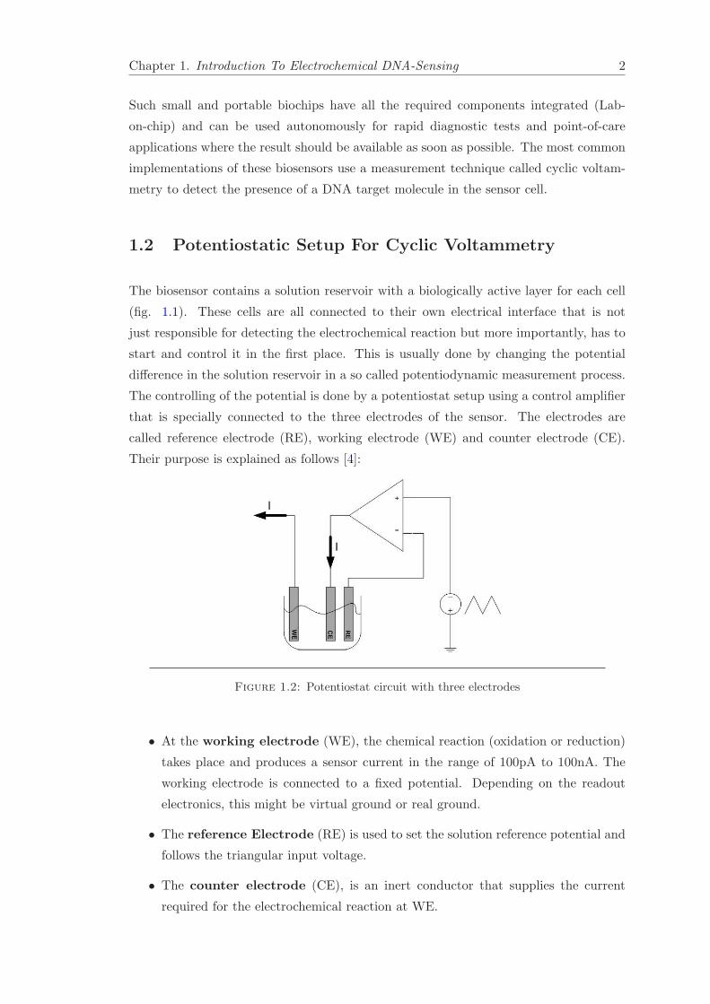
1.2 Potentiostatic Setup For Cyclic Voltammetry
The biosensor contains a solution reservoir with a biologically active layer for each cell
(fig. 1.1). These cells are all connected to their own electrical interface that is not
just responsible for detecting the electrochemical reaction but more importantly, has to
start and control it in the first place. This is usually done by changing the potential
difference in the solution reservoir in a so called potentiodynamic measurement process.
The controlling of the potential is done by a potentiostat setup using a control amplifier
that is specially connected to the three electrodes of the sensor. The electrodes are
called reference electrode (RE), working electrode (WE) and counter electrode (CE).
Their purpose is explained as follows [4]:
Figure 1.2: Potentiostat circuit with three electrodes
• At the working electrode (WE), the chemical reaction (oxidation or reduction)
takes place and produces a sensor current in the range of 100pA to 100nA. The
working electrode is connected to a fixed potential. Depending on the readout
electronics, this might be virtual ground or real ground.
• The reference Electrode (RE) is used to set the solution reference potential and
follows the triangular input voltage.
• The counter electrode (CE), is an inert conductor that supplies the current
required for the electrochemical reaction at WE.

Chapter 1. Introduction To Electrochemical DNA-Sensing 3
Because the input voltage changes in time according to a triangular signal, it causes the
potential difference WE-RE to follow accordingly. This measurement technique is also
called cyclic voltammetry and is used very frequently in amperometric (e.g. current)
measurement. There are basically three possibilities to configure the potentiostat. The
most popular one is the grounded WE configuration (figure 1.2, figure 1.3 on the left),
and is equivalent to the grounded RE configuration since both follow the input signal.
The third configuration with a grounded CE, is not considered any further for this
project, because it needs additional components and is more complex [4].
Figure 1.3: Grounded WE potentiostat, current sensing configuration, source: [4]
Since the current, that appears on the WE is very small and sensitive, it cannot be
measured directly. Therefore a transimpedance amplifier is needed to convert the current
into a larger voltage (figure 1.3, right side). Working directly with the sensor current
has several disadvantages, e.g. connection of WE only to a virtual ground. In some
cases when there is only oxidation, or only reduction, it might be better to use a current
mirror topology, and to analyze a copy of the sensor current instead. Unfortunately,
in our application the current from the DNA biosensor is bidirectional, that’s why the
optimized current mirror based potentiostat proposed in the paper from Ahmadi [4] is
not a useful possibility for the DNA biosensor.
1.3 Electrochemical Reaction
During a cyclic voltammetry sweep, a triangular input voltage signal is applied to the
control amplifier. With the DNA biosensor application in mind, the frequency and am-
plitude are defined as 0.05 Hz and ± 0.5 V. This corresponds to a slope of ± 25mV/s
which is an important key parameter in electrochemical measurements. The frequency
has to be low enough, to ensure that the reaction in the biosensor can take place. De-
pending on it’s application, the working electrode (gold electrode) is specially prepared
having immobilized single stranded DNA probes (ssDNA) mounted on the surface. This

Chapter 1. Introduction To Electrochemical DNA-Sensing 4
ssDNA contains the complementary genetic code of the sequence that should be de-
tected by the biochip. The solution, that is added into the reservoir, contains DNA
target molecules that are either complementary or not. If they are, hybridization oc-
curs, and the target molecules connect with the surface immobilized probes.
After this hybridization, the cyclic voltammetry process starts. During one sweep, the
potential difference WE-RE starts to rise. When the Odixation potential is reached, a
marker molecule (e.g Ferrocene) undergoes a one electron oxidation, thus releases an
electron and produces the oxidation peak with a forward current out of the working
electrode. Afterwards, during the ramp down of the input voltage, the marker molecule
reduces, thus takes up the electron and reverses the reaction. The current flows then
back into the sensor and the reduction peak is captured in the voltogram (fig. 1.5). In
case of hybridization (matching of target and probe), the marker molecules are much
nearer to the WE surface and therefore producing an oxidation/reduction peak, that
is clearly visible in the voltogram. Whereas in the non binding case there is no visible
peak. Repeating this cycle for several times, allows to deduce from the voltogram the
presence and concentration of a certain complementary DNA sequence in the analyte.
Figure 1.4: Working elec-trode showing probe and tar-
getFigure 1.5: Voltogram, showing oxidation and
reduction peak

Chapter 2
Comparison Of Different
Architectures
As it was stated before, the sensor current at the working electrode is very small and
sensitive. To measure it as accurately without interference and to convert it into a digital
signal is thus crucial for the performance of the biosensor. In this chapter, several ADC
topologies will be discussed. The simulation will be performed using ideal components
from the design Kit (hk370) of Austria Microsystems using .35u Technology. The voltage
references vdd and vss are at ±1.65 V.
2.1 Dual Slope ADC (fixed time integration)[1]:
The schematic of the dual slope integration ADC is shown in Appendix A.1. Each
sampling period works in two phases. First, the input current is integrated over a fixed
time interval leading to a change of the output voltage UI . Then the input current
(working electrode) is disconnected and a reference current source with opposite sign is
triggered to discharge the voltage until it reaches again 0 Volt .
The Time to discharge the capacitor will be counted with a high speed reference clock
and allows to calculate the input current.
UI = − 1
C
∫ t1
0
Iindt−1
C
∫ t2
0
Irefdt = 0
Assuming a constant input current Iin and reference current Iref for the small sampling
interval yields
− 1
C· Iin · t1 −
1
C· Iref · t2 = 0
5

Chapter 2. Comparison Of Different Architectures 6
Figure 2.1: Integration and Discharging phase for two different currents.
putting the fixed integration time as: t1 = (Zmax + 1)T and the discharging time as
t2 = Z · T with Z the number of Cycles leads to:
− 1
CIin(Zmax + 1) · T − 1
CIrefZ · T = 0
1C
and T can be crossed out. The number of discharging cycles Z can then be expressed
as follows:
Z = − IinIref
· (Zmax + 1)
solving for the input current gives finally:
Iin = − Z
Zmax + 1· Iref
2.1.1 Sizing The Architecture
The biosensor will produce currents in the range of Imin=100pA to Imax=100nA. There-
fore in case of maximum input current, the reference sources must be chosen with the
same magnitude Imax to be able to discharge the capacitor in time t2 = t1. Choosing the
size of the capacitor is crucial for the maximum current. Having Imax=100nA applied to
an integrator with 15pF capacitance takes around 250ms to reach 1.65V at the output:
i = C · dudt
assuming constant input current and solving for ∆t:
∆t =C · Uimax
=15pF · 1.65V
100nA= 247.5µs
Having a smaller input current applied, will charge the capacitor only partially. After a
proportionally shorter time the discharging will be finished. The following currents have

Chapter 2. Comparison Of Different Architectures 7
been simulated using a fixed integration time of 250µs and constant reference current
sources of ± 100nA. Since the input current (sensor current from the working electrode)
is applied to the negative terminal of the integrator according to Levine[1], the output
voltage of the integrator UI drops as shown in the simulation:
Figure 2.2: UI -Voltage in function of different currents [100nA, 50nA, 25nA, 12.5nA,6.25nA, 3.125nA, 1.5625nA]
Sampling the discharging time t2 and counting the number of periods (Z) until the
capacitor is discharged allows to calculate the input current. Using a 10bit counter
(Zmax = 1024) and sampling frequency of 4MHz allows to cover currents from 100nA
down to 100pA in the 250µs discharging window.
2.1.2 Discussion Of The Dual Slope Integrator
The architecture is very scalable, and the main parameters like integrator capacitor,
sampling frequency and resolution can be easily adjusted. But the architecture has also
some disadvantages: Many control signals and clocks are needed. For example a low
frequency clock to start and stop the integration phase, a high speed clock to count the
time of the discharging phase, a start and stop signal for the counter and finally a reset
signal for the counter. All these signal have to be put together into a control block (state
machine) which makes simulation in the cadence analog design environment more tricky.
Then for small currents, the resolution is rather poor, because the discharging phase is
very short (figure 2.2). The most serious disadvantage is, that in case of small input
currents, the waiting time is very long until the next sampling period starts. Therefore
the architecture does not seem very efficient in terms of resolution (sampling points)
and accuracy for low input currents.
Chapter 2. Comparison Of Different Architectures 8
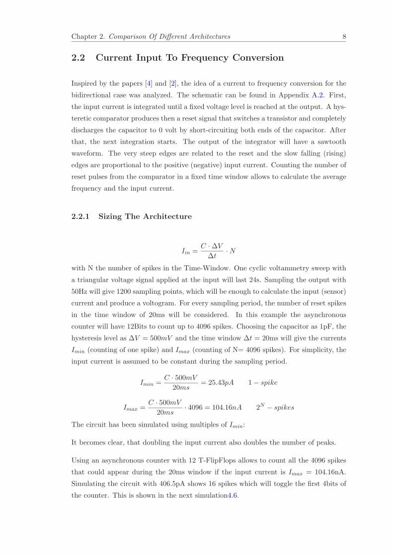
2.2 Current Input To Frequency Conversion
Inspired by the papers [4] and [2], the idea of a current to frequency conversion for the
bidirectional case was analyzed. The schematic can be found in Appendix A.2. First,
the input current is integrated until a fixed voltage level is reached at the output. A hys-
teretic comparator produces then a reset signal that switches a transistor and completely
discharges the capacitor to 0 volt by short-circuiting both ends of the capacitor. After
that, the next integration starts. The output of the integrator will have a sawtooth
waveform. The very steep edges are related to the reset and the slow falling (rising)
edges are proportional to the positive (negative) input current. Counting the number of
reset pulses from the comparator in a fixed time window allows to calculate the average
frequency and the input current.
2.2.1 Sizing The Architecture
Iin =C ·∆V
∆t·N
with N the number of spikes in the Time-Window. One cyclic voltammetry sweep with
a triangular voltage signal applied at the input will last 24s. Sampling the output with
50Hz will give 1200 sampling points, which will be enough to calculate the input (sensor)
current and produce a voltogram. For every sampling period, the number of reset spikes
in the time window of 20ms will be considered. In this example the asynchronous
counter will have 12Bits to count up to 4096 spikes. Choosing the capacitor as 1pF, the
hysteresis level as ∆V = 500mV and the time window ∆t = 20ms will give the currents
Imin (counting of one spike) and Imax (counting of N= 4096 spikes). For simplicity, the
input current is assumed to be constant during the sampling period.
Imin =C · 500mV
20ms= 25.43pA 1− spike
Imax =C · 500mV
20ms· 4096 = 104.16nA 2N − spikes
The circuit has been simulated using multiples of Imin:
It becomes clear, that doubling the input current also doubles the number of peaks.
Using an asynchronous counter with 12 T-FlipFlops allows to count all the 4096 spikes
that could appear during the 20ms window if the input current is Imax = 104.16nA.
Simulating the circuit with 406.5pA shows 16 spikes which will toggle the first 4bits of
the counter. This is shown in the next simulation4.6.

Chapter 2. Comparison Of Different Architectures 9
Figure 2.3: Vint simulated for Iin= 25.43pA, 50.86pA, 101.72pA, 203.44pA, 406.5pA.
Figure 2.4: The first four bits toggle when counting up to 16).
2.2.2 Discussion
At first this architecture seems not very attractive because two comparators are needed
which requires additional Si area for the final layout. But on the other hand the inte-
gration capacitor is much smaller which might compensate the additional area of the
2nd comparator. Another advantage is that the control signals (rst, comparator output
signals, ...) are basically not depending on each other. Therefore no control block with

Chapter 2. Comparison Of Different Architectures 10
a finite state machine is needed and the whole circuit can be easily simulated. The
resolution for small currents is very good.
2.3 Semi Synchronous Σ∆-ADC [2]
The circuit proposed by A.Gore uses only one hysteretic comparator and therefore re-
duces the size considerably. The idea is basically an improvement of the conventional
Σ∆-ADC, that is used in many applications. Major drawback of the conventional Σ∆-
ADC is the high switching rate, which increases substrate noise and power consumption.
To reduce the switching rate, a hysteretic comparator is introduced. But adding hystere-
sis has also a drawback: At the end of the synchronous Σ∆-Phase the integrator voltage
stays in an unknown state anywhere between ±∆ V. This voltage, also called residue,
will be added up in the following sampling cycles, leading to an error trail bounded by
the threshold voltages of the comparator. To avoid this error, a second asynchronous
phase is proposed. During this 2nd phase, which is also called extended counting or
compensation step, the remaining voltage will be charged/discharged using only the ref-
erence current to a known value. This extended counting phase or compensation step
allows to start the next cycle from a known state and permits to increase the resolution
by one additional bit.
Figure 2.5: architecture proposed by A.Gore.
The schematic has been done using the 250mV hysteretic comparator from the previous
architecture and a capacitance of 15pF. Transmission gates are chosen as switches to
connect and disconnect the working electrode or reference current sources, because of
their high resistance in non-conducting state.

Chapter 2. Comparison Of Different Architectures 11
Figure 2.6: Transmission Gates as switches.
During the synchronous phase the integrator voltage at each clock cycle can be expressed
as.
Un = Un−1 +
(
IinIref
−Dn
)
IrefTclk
C
Dn = sign (Un−1 +Dn−1∆)
(2.1)
In the extended counting phase, the working electrode is disconnected and the integrator
is charged/discharged only by the reference current until the comparator switches from
1 to -1. The output voltage can then be expressed by:
U∗
n = U∗
n−1 −Dn
IrefTclk
C
D∗
n = sign (Un−1 +Dn−1∆)
(2.2)
with Dn ∈ {−1,+1} being a variable for the logic levels of the comparator as low and
high. Using directly the comparator output to control the switching of the reference
current sources allows to turn -Iref on with Dn high, respectively +Iref with Dn low.
By defining the start state U0 of the synchronous counting phase and the end state of
the extended counting phase UNext as equal, and for example +∆2volt, allows to write
the equations 2.1 and 2.2 as:
UN = U0 +
(
IinIref
−N∑
n=1
Dn
)
Iref · Tclk
C
UNext = UN −Next∑
n=1
D∗
n · Iref · Tclk
C(= U0)

Chapter 2. Comparison Of Different Architectures 12
using the two formulas and solving for Iin allows finally to solve for the sensor current:
Iin =
(
N∑
n=1
Dn +
Next∑
n=1
D∗
n
)
· IrefN
+ errorterm
2.3.1 Discussion
The semi-synchronous Σ∆ conversion proposed by A.Gore [2] is a very nice and area
efficient implementation. It reduces considerably the switching rate compared to con-
ventional Σ∆-ADC and is very power efficient. Unfortunately it requires a lot of control
signals such as start/stop of synchronous phase, start/stop of extended counting phase,
a synchronous up/down counter with a reset, a multiplexer and two memory cells for
ΣD and Σ D∗ of the two phases. The simulation and testing turned out to be too
complicated and therefore this architecture was not considered for final implementation.
But it would definitely be the most promising architecture, with high resolution, high
sensitivity, low power and small area.

Chapter 3
Experimental Setup Of Current
To Frequency Conversion
Technique
After simulation and detailed analysis of the three different architectures, the current
to frequency technique from section 2.2 was chosen for final implementation. The ad-
vantages where mainly, that the circuit runs on it’s own, without many control signals
that depend on each other. Therefore the simulation turns out be very simple. For the
final implementation, the decision was made, to move from the Austria Microsystems
process AMS.35 to the newer UMC.18 fabrication. Reasons where primarily the cheaper
production costs due to the other designs in the LSM lab which will all be fabricated on
the same wafer using the same UMC.18 process technology.
3.1 Top Level Schematic Of The Circuit
Moving from AMS.35u technology to the UMC.18u made a lot of changes necessary.
The reduction of the biasing voltage from ±1.65 V down to ± 900mV, required the
recalculation of all parameters with the new model parameters. Then certain schematics
of components such as D-FF and T-FF where no longer available from a library and
had to be redone. The overall circuit showing all the different sub-blocks is shown in
fig. 3.1.
13

Chapter 3. Experimental Setup Of Current To Frequency Conversion Technique 14
Figure 3.1: Toplevel of current to frequency conversion circuit
3.2 Sizing Of The Overall System
The system was sized to be able of converting currents in the range from 100pA to
100nA. Choosing the hysteresis level and capacitor size allows to adapt the circuit to
this specification.
Imin = C · dUdt
corresponds to one peak in the sampling window. Assuming constant input current
allows to write:
Imin = C · U∆t
and to solve for the sampling period ∆t:
∆t =C ·∆V
Imin
=1pF · 250mV
100pA= 2.5ms
When the maximum current is applied, the number of peaks in the sampling period will
increase to it’s maximum of 210 with each peak reaching the comparator threshold after
≈ 2.5µ s. Using this values, allows to get a 10bit number out of the counter with a
frequency of f = 12.5ms
= 400Hz. This corresponds to 8000 measurement points during
one cyclic voltammetry sweep, which is enough to draw the voltogram:
Tcyclicvoltammetrysweepperiod
Tsamplingperiod
=20s
2.5ms= 8000

Chapter 4
Building Blocks In .18u
Technology
The building blocks are implemented using the standard transistors from the UMC 18 CMOS
library. VDD and VSS are defined as±900mV and therefore the transistor P 18 MM
and N 18 MM are chosen.
4.1 Comparator
Usually hysteresis is added to a comparator by using an input resistor R1 and and
feedback resistor R2. The Threshold voltages are then given by 1:
V +th = Vdd ·
R2
R1 +R2
V −
th = Vss ·R2
R1 +R2
(4.1)
However, there are several disadvantages using external resistors. First they have to be
large in order not to influence the current flow inside the comparator. Second, they will
occupy a lot of chip area and might not have the exact expected value due to process
variations. Third they build a large resistive load, that has to be driven by the output
of the comparator or the output of the integrator op amp. Therefore a much more
suitable implementation is chosen with internal feedback resistances. It occupies much
less area and consumes less power. The two differential input pair transistors (NM1,
NM2) are building a negative feedback from the output back to the input. The four
PMOS transistors on top (PM1, PM2, PM3, PM4) create a positive feedback.
1http://www.maxim-ic.com/app-notes/index.mvp/id/3616
15

Chapter 4. Building Blocks in .18u Technology 16
Figure 4.1: ∆ 250mV hysteretic comparator
4.1.1 Sizing Of The Transistors
Because the analog comparator is very sensitive to process variations, the gate length is
chosen to be three times larger than the minimal gate length. By doing this, the small
variations in the transistor dimensions have much less impact on the behavior of the
transistor. The model parameters are shown in Appendix C.1.
Biasing Circuit
The transistor NM3 has to be in strong inversion and saturation for a desired biasing
current of 10uA. The inversion factor is therefore chosen to be around 40 for very strong
inversion. The ratio can be calculated as:
(
W
L
)
NM3
=10µA
2 · nµCox · IF · U2t
≈ 1.54 ≈ 820
540
The transistor in the left branch, has a 10 times larger WL
ratio in order to conduct a
ten times larger current:
(
W
L
)
NM4
=100µA
2 · nµCox · IF · U2t
≈ 1.54 ≈ 8200
540
Chapter 4. Building Blocks in .18u Technology 17
The large width is divided up into 10 fingers to get a better aspect ratio2. The voltage
difference between vdd and the drain of NM4 is still relatively large. Therefore a high
resistor would be needed to generate a small current of 100uA. To reduce the high value
of the resistor and thus the layout size, an additional diode connected transistor is in-
serted. This transistor MN5 with the same dimensions as MN4 produces an additional
voltage drop and allows to decrease the resistor considerably by having the same current
100uA.
Comparator Circuit
The comparator function is implemented by the negative feedback transistor (NM1,
NM2) and the positive feedback transistors (PM1, PM2, PM3, PM4). The NMOS
transistors are also sized to operate in strong inversion and saturation, but this time the
current that flows through the transistors is only 5uA. The inversion factor IF is chosen
to be around 30, to get a nice ratio of:
(
W
L
)
NM1,NM2
=I02
2 · n · µ · Cox · IF · U2T
≈ 1 ≈ 720n
720n
The remaining PMOS positive feedback transistors (PF3, PF4, PF5, PF6)have to be
sized in order to get the desired feedback factor which in return defines the hysteresis
level 3.
Vth = V ref ±√
2 · n · IBias
β
(√k − 1√k + 1
)
Solving for k and considering a hysteresis of ∆ 250mV and βNM1,NM2 = KP · WL
defines
k as 3.35. this Feedback factor k is defined by the ratio of
k =W/LPM2
W/LPM1
=W/LPM3
W/LPM4
=2412/540
720/540= 3.35
. Simulation with these values and a reference at zero volt, makes the comparator switch
around ±118mV. Therefore the width W of PM2 and PM3 are slightly increased to get
switching later at ± 125mV.
k1 =W/LPM2
W/LPM1
=2620/540
720/540k2 =
W/LPM3
W/LPM4
=2680/540
720/540
2common method to reduce the aspect ratio of large transistors3lecture notes Analog 2, Prof.Maher Kayal, EPFL 2010

Chapter 4. Building Blocks in .18u Technology 18
The increase of the feedback factor (the width of PM2 and PM3) seems to be necessary,
because the bulk of the input differential pair cannot be connected to its source as it is
shown in the lecture notes4. For the layout the bulk of all NMOS transistors have to be
connected to the lowest potential (vss).
Output Stage
To get a rail to rail single ended output of the comparator, a special output stage is
needed consisting of the transistors PM5, PM6, NM6 and NM7. This output stage
provides reasonable voltage swing and output resistance. The chosen topology makes a
conversion from differential input to single ended output [5]. Because the load of the
comparator is not expected to be very large, the capacitive drive is not further increased
with an inverter chain. The transistor sizes of the output stage are chosen to be three
times larger then the minimum dimensions:
(
W
L
)
PM5,PM6,NM6,NM7
=720
540
The final dimensions in [nm] for the comparator are:
PM1 PM2 PM3 PM4 PM5 PM6 R
W 720 2620 2680 720 720 720 1000
L 540 540 540 540 540 540 3670
Table 4.1: PMOS Transistor Sizes for comparator
NM1 NM2 NM3 NM4 NM5 NM6 NM7
W 720 720 820 8200 8200 720 720
L 720 720 580 580 580 950 950
Table 4.2: NMOS Transistor Sizes for comparator
The simulation result of this comparator is shown in Appendix B.1.
4.2 3-level Comparator Block
Two of the above comparators are used to form a three level hysteretic comparator
Block. The upper comparator produces a signal D1, that rises to high, as soon as the
input exceeds the upper threshold at 250mV, and will be set back when the input voltage
reaches 0V again (lower threshold). Similar is the behavior of the lower comparator. If
4lecture notes: Analog 2 of Prof. Maher Kayal, EPFL 2010

Chapter 4. Building Blocks in .18u Technology 19
the input voltage decreases below -250mV the signal is going high, but as soon as it rises
above 0V it changes to low again (fig 3.4).
Figure 4.2
Figure 4.3: input outputtransfer characteristic of 3level hysteretic comparator
block
Unfortunately by applying the reference voltage ± 125mV to the comparators, the turn-
ing points change slightly due to unsymmetry of the circuit. It’s therefore necessary to
change again the sizes of the positive feedback resistor PM1, PM2, PM3 and PM4 for
the upper and the lower comparator. The final values after some simulations yields:
PM1 PM2 PM3 PM4
W 720 2570 2590 720
L 540 540 540 540
Table 4.3: comparator producing D1
PM1 PM2 PM3 PM4
W 720 2900 2650 720
L 540 540 540 540
Table 4.4: comparator producing D2
The simulation of the changed schematic with optimized transistor sizes shows the right
behavior for the signals D1 and D2. Those two signals will later be used to trigger the
reset of the integrator capacitor. Because the reset happens very fast, the comparators
will only produce very short pulses (spikes) at the output.
Chapter 4. Building Blocks in .18u Technology 20
Figure 4.4: Simulation results of 3 level Comparator Block
4.3 Sign Detection Block
Counting the number of these spikes in a fixed time window will provide just informa-
tion about the magnitude of the current. To make a decision about its direction, it
becomes necessary to make a distinction between spikes from each comparator output.
The simplest idea would be to use two counters, one for each comparator output. By
observing the total number of spikes from D1 and D2 it becomes possible to make a
decision about the direction of the current during that sampling interval.
ΣD1 > ΣD2: the current is negative
ΣD1 < ΣD2: the current is positive
ΣD1 = ΣD2: the current is 0 A
This implementation is not very efficient because two 10bit counters require a lot of
space. But by taking into account that the input current varies only slowly during one
sampling period, the problem can be simplified. In most of the samples, the spikes come
all from one comparator output while the other one does not produce spikes. Therefore
it’s no problem to sum up both spikes from D1 and D2 with the same counter. The
only problem arises when the current direction changes within a sampling period and
produces first spikes in one comparator, and then afterwards in the second. But this
case is very rare and occurs just in the zero crossing points of the voltogram (fig. 1.5).

Chapter 4. Building Blocks in .18u Technology 21
The idea of the simplification is to observe which comparator produced the first spike,
and to decide with this information the sign of the current. After that, all spikes re-
gardless of which comparator output, are summed up and provide the magnitude of the
current during that sample.
The following circuit is used to detect which comparator produced the first spike. The
D-FF, XOR and inverter where done using minimal dimension transistors because the
digital circuit is not that much sensitive to process variations. The schematic of the
D-FF is shown in Appendix A.3.
Figure 4.5: Edge detection circuit to sense the direction of the current
The two Delay FF and the XOR Gate form an edge detection circuit with output Q1
(Q2). This output will be reset after every sampling period with an active low signal.
The output Q1(Q2) goes high, when two conditions are fulfilled: the first spike comes
from D1(D2) and the other circuit has not detected a spike yet Q2N (Q1N).
The simulation results that where obtained explain the idea:
The current direction bits Q1 and Q2 are reset after every 300us with an active low reset
signal. Depending on the first spike (marker A or B) one of these two bits is set to high,
and prevents the other bit of going high in the same sample period as it is shown in the
period after the 4th reset.
4.4 Counter Block
Both comparator outputs are connected through an XOR-gate to the counter. This
10Bit counter detects all the spikes, regardless from which comparator they are coming
and will be reset after each sampling Period. The number of spikes is used to calculate

Chapter 4. Building Blocks in .18u Technology 22
Figure 4.6: Simulation of sign detection circuit
the magnitude of the sensor current during each sampling period. The counter is imple-
mented using 10 toggle flipflops with an active low reset. The schematic of the T-FF is
shown in Appendix A.4.
The Counter has been simulated to count up to 1000 and was then reset with an active
low RST signal at around 19ms. All the 10 output ports will be connected to the negated
output of its Toggle FF, to get a binary up counter.
Figure 4.7: Simulation result, counting up to 1000

Chapter 4. Building Blocks in .18u Technology 23
It’s important to note, that the reset signal puts the counter back into its initial state
[111...1] and the first spike will be denoted with output vector [000...0]. The number of
counted spikes is therefore always equal to the output of the counter +1.

Chapter 5
Layout
According to the project description, it was planned to draw the layout of the overall
system. But the migration from AMS.035 to UMC.18 Technology turned out to be very
time consuming. Because the schematics and layout of the FF are no longer available,
the layout of the sign detection block and counter was not done. For the final simulation
of the overall system, the schematic will be used instead for these missing blocks.
5.1 Layout Of The Comparator
Drawing the layout of the comparator required several trials and changes in the schematic.
The ideal resistor had to be changed into a real resistor (rnrhm1000 mm) from
UMC18 CMOS library. Then the biasing current mirror had to be sized properly with
a finger structure for the transistors NM4 and NM5. Also the input differential pair
transistors had to be changed with their bulk connection to vss. This made resizing of
the feedback transistors necessary. After solving these problems in the schematic the
layout was started. The transistors where arranged trying to keep the arrangement of
the schematic whenever possible. This allows the current to flow in one direction from
vdd to vss. Also the high current from the biasing circuit was put to the side like in
the schematic, in order not to interfere with the sensible comparator. The PMOS are
mostly on top near vdd and in the n-well, and the NMOS are more on the bottom near
the vss contacts. The layout was finally compressed as much as possible using minimal
distances between the metal lines, transistors, contacts, ...
24

Chapter 5. Layout 25
Figure 5.1: Layout after passing DRC check
Figure 5.2: Transistor placement
Figure 5.3: Extracted layout showing parasitic capacitances and resistors

Chapter 6
Simulation Results And
Discussion Of The Overall System
6.1 Putting It All Together
The overall system was put together using the extracted layout of the integrator op
amp1 and the 3 level comparator block. The other parts, such as sign detection block
and counter, where simulated using their schematic in place of the missing layout.
Figure 6.1: Final system showing all blocks
The final system in fig:6.1 has some minor changes compared to the schematic in chap-
ter3 fig:3.1. The six transistors in front of the op amp are necessary for the disconnection
of the WE from the readout electronics during the reset of the integrator. The disconnec-
tion of the WE happens when either D1, D2 or RST is high, thus building a connection
through one of the three parallel NMOS transistors to ground. In all other cases, the
path to ground is open, and the three serial NMOS switches are closed (D1∧D2∧RST )
1work of Gmel Gerrit, working on the same topic
26
Chapter 6. Results and Discussion 27
leading the current directly to the integrator. By applying this principle, the shorting
of the integrator capacitor, does not influence the working electrode.
6.1.1 Sizing Of The Reset Transistors
Another thing that had to be changed, was the size of the reset transistors for shorting
the capacitor. Using minimum dimensions provided first very disappointing results. The
reset happened too fast with an undershoot of nearly 100mV. The Comparator switched
then back to zero, and the next integration started from -100mV instead of zero volt.
Therefore the sizes had to be changed to around WL
= 240n2.3u
in order to increase the
resistance. The reasoning was, that the RC time constant should be increased so that
the reset takes more time, goes slower to 0V without a large (over)undershoot. This
resizing also helped to increase the pulse width of the comparator signals D1 and D2
from 30ns to 190ns. This was in fact considered an advantage, since the setup times of
the D-FF and T-FF where not checked. Simulation results where obtained for a 200pA
current, thus producing 2 spikes within the sampling window. A detailed zoom of the
spike at around ≈ 1.25ms is shown in Appendix B.2.
6.2 Simulation Results
Several simulations where performed using different input currents. Applying 100pA
should produce 1 spike in the 2.5ms time interval and defines also the resolution limit
of this architecture. Increasing the current should lead to proportionally more spikes.
This behavior was verified using multiples of Imin as it is shown in 6.2:
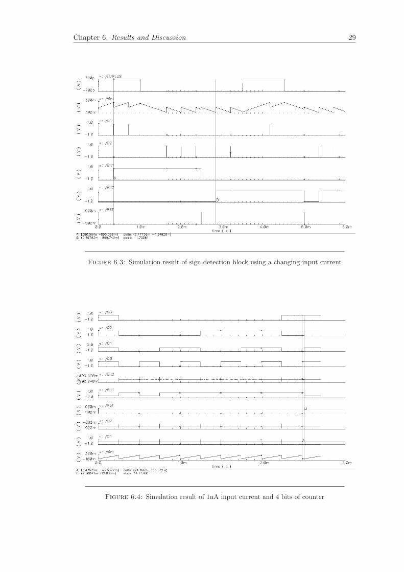
The behavior of the sign detection block is simulated by applying an input current that
changes from +700pA to -700pA within one sampling period. It is shown, that the first
spike coming from D1 sets Bit1 and prevents the other bit from going high in the same
sampling period until it is reset by the RST signal. In the second sampling period it’s
shown that the first spike coming from D2 sets Bit2 until it is again reset at 5ms. The
result of this simulation is shown in fig: 6.3.
Applying higher currents at the input was used to check if the counter is working and
if the accuracy of the overall system holds up to the expectations. Simulation with
1nA, corresponds to 10 times the minimal current Imin and produces 10 spikes. The
counter, which after the initial reset is in state [11...1] changes with the first spike into
[00...0]. For the next 9 spikes he is continueously incremented to 9, which is shown in
the simulation (fig. 6.4) by the waveforms [Q0, Q1, Q2, Q3].

Chapter 6. Results and Discussion 28
Figure 6.2: Simulation result of integrator voltage and comparator output for multi-ples of Imin [100pA, 200pA, 300pA, 400pA, 500pA] from bottom to top
Using the maximum current, produces a large number of peaks as shown int fig. 6.6.
By zooming in, it is shown, that the final values of the counter is not near to 1000. It
only shows someting around 768 with [Q0, ...Q9]= [1111111101].
The accuracy is therefor not quite satisfying. Due to the sizing of the reset transistors
(section 6.1.1) the error has increased. The reset time can not be ignored anymore for
high currents, and has to be included for the calculation and timing. If for example
1024 spikes where counted during the sampling period, then the overall reset time of
all spikes is about: ≈ 1024 · 350ns = 358.4µs which corresponds to approximately one
spike missing in the end of the sampling period, and an error of Imin. Another problem
concerns the accuracy of the 3 level comparator block. When tested seperetly, it worked
very accurate 4.4. But in the final system, the input waveform is different. Instead of
the triangular signal between vss and vdd, there is now a sawtooth input signal, that
barely crosses ±250mV . Simulating with Imin showed that the comparator switched
already at 248mV up and 0 V down. For Imax it switched at 250mV up and 2mV down.
Therefore the comparator behaves slightly different, depending on the input current
and its corresponding sawtooth signal Vint. These effects have to be included in for the
interpretation of the counter output.
Chapter 6. Results and Discussion 29
Figure 6.3: Simulation result of sign detection block using a changing input current
Figure 6.4: Simulation result of 1nA input current and 4 bits of counter

Chapter 6. Results and Discussion 30
Figure 6.5: Simulation result of 100nA, showing the ten bits of the counter
Figure 6.6: Simulation result of 100nA, showing the ten bits of the counter at 2.5ms

Chapter 7
Conclusion
The electrical interface for an electrochemical biosensor array was examined. Three
topologies where simulated using ideal components from .35µ design kit of Austria Mi-
crosystems. For the final implementation using the UMC.18 process technology, the
current to frequency conversion technique was chosen. This architecture was imple-
mented using only NMOS and PMOS transistors from SP 018 library. The layout of
opamp1 and comparator block was drawn. The final simulation results where obtained
using the extracted layouts of op amp and comparator block. The other parts such as
counter and sign detection block where simulated with the schematic.
7.1 What Remains To Be Done
Unfortunately, the intention to draw the layout of the overall system was too ambitious.
The sign detection block and counter layout will have to be done in a later step. Also
the error calculation and estimation could be done more seriously. So that the system is
more accurate for high currents. The timing of the reset phase and the exact switching
of the comparator will be necessary to get the best performance out of this architecture.
Very crucial for the performance will be the noise analysis. Since the application uses
very low frequencies, the 1fstarts to play an important role and begins to dominate over
the thermal noise. On a higher level, the sample points can be interpolated to get a
smooth voltogram curve. Time multiplexing of the different sensor cells can help to save
hardware space and power. Also the error that was introduced before by adding the
spikes from D1 and D2 with the same counter, might be further reduced by averiging
the sample point at the zero crossings of the voltogram.
1work of Gmel Gerrit, working on the same topic
31

Appendix A
Schematics
Figure A.1: Dual Slope Architecture proposed by Levine [1]
Figure A.2: Current to frequency conversion (bidirectional)
32

Appendix 1. schematics 33
Figure A.3: schematic for D-FF, from A-Cells library of Austria Microsystems)
Figure A.4: schematic of a T-FF, from A-Cells library of Austria Microsystems)

Appendix B
Simulation Results
Figure B.1: Simulation results of the Comparator with 250mV hysteresis andVref=0V
34

Appendix 2. parameters 35
Figure B.2: Comparison of reset transistors with minimal dimensions and optimizedvalues

Appendix C
UMC.18 Model Parameters
Figure C.1: Model parameters for UMC.18 process technology, source
36

Bibliography
[1] Peter M Levine, Student Member, Ping Gong, Rastislav Levicky,
and Kenneth L Shepard. Active CMOS Sensor Array for Elec-
trochemical Biomolecular Detection. 43(8):1859–1871, 2008. URL
http://bioee.ee.columbia.edu/downloads/2008/ActiveCMOSIEEE.pdf.
[2] Amit Gore and Shantanu Chakrabartty. A Multi-channel
Femtoampere-sensitivity Conductometric Array for Biosens-
ing Applications. New York, pages 6489–6492, 2006. URL
http://ieeexplore.ieee.org/stamp/stamp.jsp?arnumber=04012346.
[3] Andrew Mason, Yue Huang, Chao Yang, and Jichun Zhang. Amperometric Readout
and Electrode Array Chip for Bioelectrochemical Sensors. Test, pages 3562–3565,
2007.
[4] Mohammad Mahdi Ahmadi, Graham A Jullien, and Life Fellow. Current-
Mirror-Based Potentiostats for Three-Electrode Amperometric Elec-
trochemical Sensors. Configurations, 56(7):1339–1348, 2009. URL
http://ieeexplore.ieee.org/stamp/stamp.jsp?arnumber=04629303.
[5] Phillip E. Allen and Dougls R. Holberg. CMOS Analog Circuit Design. Oxford
University Press, 2nd editio edition. ISBN 0-19-511644-5.
37
Related Documents