CONTROL AND POWER MANAGEMENT SCHEMES FOR DISTRIBUTED AND BATTERY POWERED SYSTEMS by WANGXIN HUANG JABER ABU QAHOUQ, COMMITTEE CHAIR TIM A. HASKEW KENNETH G. RICKS FEI HU KEITH A. WILLIAMS A DISSERTATION Submitted in partial fulfillment of the requirements for the degree of Doctor of Philosophy in the Department of Electrical and Computer Engineering in the Graduate School of The University of Alabama TUSCALOOSA, ALABAMA 2016

Welcome message from author
This document is posted to help you gain knowledge. Please leave a comment to let me know what you think about it! Share it to your friends and learn new things together.
Transcript
CONTROL AND POWER MANAGEMENT SCHEMES FOR
DISTRIBUTED AND BATTERY POWERED SYSTEMS
by
WANGXIN HUANG
JABER ABU QAHOUQ, COMMITTEE CHAIR
TIM A. HASKEW KENNETH G. RICKS
FEI HU KEITH A. WILLIAMS
A DISSERTATION
Submitted in partial fulfillment of the requirements for the degree of Doctor of Philosophy in the
Department of Electrical and Computer Engineering in the Graduate School of
The University of Alabama
TUSCALOOSA, ALABAMA
2016

Copyright Wangxin Huang 2016 ALL RIGHTS RESERVE
ii
ABSTRACT
Battery systems are widely used in many applications including portable electronics,
EVs/HEVs, and distributed smart power grids. In addition to battery technologies, the battery
management system (BMS) plays a critical role in enabling the widespread adoption of battery-
powered applications. This dissertation work focuses on addressing several issues and improving
performance of several aspects of battery powered applications. These focused topics include
online monitoring of battery impedance, charge balancing between battery cells during both
discharging and charging operation, and power electronic topologies and control in order to
improve reliability, efficiency, and density of the battery-powered applications.
In chapter 2, a practical method is presented in order to achieve accurate online battery
impedance measurement while maintaining output voltage regulation of the power converter.
The proposed method is based on converter duty cycle control and perturbation. As a result, all
the external signal injection circuitries are eliminated.
In chapter 3 and 4, the charge balancing issue is addressed from the root by automatically
adjusting the discharge/charge rate of each cell based on a new distributed battery system
architecture with energy sharing control. The proposed energy sharing controller does not require
any charge/energy transfer between the cells, thus eliminating the power losses during energy
transfer process.
iii
To gain insights into the dynamics of the energy sharing controlled distributed battery
system, the state-space averaging small-signal modeling and controller design is performed in
Chapter 5. Simulation and experimental results are presented for verification.
Single-inductor multiple-output DC-DC converter has gained increased popularity in the
portable applications where a battery is used to power multiple loads. However, a common issue
facing the SIMO converter design is the cross regulation between the multiple outputs during
steady-state and dynamic operations. To address this issue, a power-multiplexed controller is
presented in Chapter 6 which eliminates the cross regulation between the outputs by
multiplexing the conduction of each output channels. Each output is independently regulated
under steady-state and dynamic operations regardless of the operating mode, i.e., continuous or
discontinuous conduction mode.
Chapter 7 summarizes this work and provides conclusions before discussing some
possible future research directions related to this dissertation work.
iv
LIST OF ABBREVIATIONS AND SYMBOLS
EVs Electric Vehicles
PHEVs Plug-in Hybrid Electric Vehicles
BMS Battery Management System
SOC
State-of-Charge
SOH State-of-Health
SIMO Single-Inductor Multiple-Output
NiMH Nickel-metal-hydride
Cavailable The amount of charges remaining in the battery
Cmax The total amount of charges when the battery is fully charged
ANN Artificial Neural Network
OCV Open Circuit Voltage
CAN Control Area Network
EIS Electrochemical Impedance Spectroscopy
HCSD Harmonic Compensated Synchronous Detection
PM Power Multiplexed
v
DCM Discontinuous Conduction Mode
CCM Continuous Conduction Mode
Voc(SOC) SOC dependent voltage source
Zbattery Impedance of the battery
fp Perturbation frequency
Vac Amplitude of the AC component of the battery voltage
Iac Amplitude of the AC component of the battery current
zϕ The phase of the battery impedance
Vo_dc DC output voltage
Ddc DC duty cycle
Vbattery_dc DC voltage of the battery
Ibattery_dc DC current of the battery
T1 Instant when impedance measurement mode is triggered
dac Small duty cycle sinusoidal perturbation signal
Dac Amplitude of the small duty cycle sinusoidal perturbation signal
Vbattery-pp Peak-to-peak value of the battery voltage
Ibattery-pp Peak-to-peak value of the battery current
vi
M Number of cycle Vbattery-pp and Vbattery-pp are measured
TH1 Threshold for Vbattery-pp
TH2 Threshold for Ibattery-pp
q Quantization error
ADC Analog-to-Digital Converter
LSB Least significant bit
Vrange Input analog voltage range of the ADC
N The number of bits of the ADC after analog to digital conversion
vϕ Phase of the AC voltage
iϕ Phase of the AC current
fsw Switching frequency
Xvalley Register in the digital controller that holds the valley value of the signal
Xpeak Register in the digital controller that holds the peak value of the signal
TI Texas Instruments Corportion
d Duty cycle of the power converter
C-rate The rate at which the battery discharges or charges normalized to the
capacity of the battery
vii
DOD Depth of discharge
OCVest Estimated OCV value of the battery
Vref Output voltage reference value of the power converter
Vref_dc DC Output voltage reference value of the power converter
Vref_ac AC Output voltage reference value of the power converter
fk Kth perturbation frequency
Ak Amplitude of the sinusoidal wave with the frequency of fk
kθ Phase delay of the sinusoidal wave with the frequency of fk
B.C. Balancing circuit
ZCS Zero-current switching
BPM Battery power module
DCR DC resistance of the inductor
ESR Equivalent series resistance of the capacitor
PCB Printed circuit board
Vbus-ref The DC bus voltage reference
Vr-ref output voltage reference for the power converter in BPMr
αvr Voltage multiplier in discharge mode
viii
Mv The sum of the voltage multiplier values in discharge mode
Vr The output voltage of BPMr power converter
Vbus DC bus voltage
Vpack Battery pack voltage
GvB(s) Continuous-time transfer function of the compensator used in the voltage
control loop in discharge mode
GvB(z) Discrete-time transfer function of the compensator used in the voltage
control loop in discharge mode
PID Proportional-Integral-Derivative
SOCv-ref The reference SOC in discharge mode
βvr The SOC balancing loop multiplier in discharge mode
Nv_active The number of active BPMs
δr Enable/Disable multipliers
Gdhgr DC voltage gain for the power converters in BPMr in discharge mode
Zcellr Zcellr is the internal impedance of the battery cellr
Vcell Cell voltage
Io Load current
ix
DPWM digital Pulse-Width-Modulation
CCCM Constant current charging mode
CVCM Constant voltage charging mode
Ic Capacity current
Vmax The maximum charging voltage of the battery
Mi The sum of voltage multipliers in charge mode
Icell-avg The average cell current in charge mode
Vcell-avg The average cell voltage in charge mode
Gchgr DC voltage gain for the power converter in BPMr
ηr Efficiency of the BPMr
Por Output power of the BPMr
Pinr Input power of the BPMr
Tvr-dhg BPMr output voltage control loop gain in discharge mode
Tsocr-dhg BPMr SOC control loop gain in discharge mode
Slr Low-side switch in BPMr power converter
Sur High-side switch in BPMr power converter
Ts Switching period of the BPM power converter
x
X Equilibrium state vector
µs Microsecond
Gvdr-dhg(s) Duty cycle control to BPMr converter output voltage transfer function in
discharge mode
Gidr-dhg(s) Duty cycle control to cellr current transfer function in discharge mode
Zor(s) Open loop output impedance of the BPMr
Gsocir-dhg Cellr current Icellr to SOCr transfer function for BPMr
T Sampling period of the SOC value
Q Rated capacity of the cell in coulomb
DPWMr modulator gain in discharge mode
uncompensated BPM output voltage loop gain in discharge mode
RHP right-half-plane
Continuous-time BPM output voltage control loop compensator in
discharge mdoe
Discrete-time BPM output voltage control loop compensator
Touter-dhg-uncomps Uncompensated outer loop gain in discharge mode
%&' Continuous-time BPM SOC control loop compensator in discharge mdoe
xi
%&' Discrete-time BPM SOC control loop compensator in discharge mdoe
Duty cycle control to BPM input voltage transfer function in charge mode
Gidr-chg(s) Duty cycle control to cellr current transfer function in charge mode
Gsocir-chg cellr current to cellr SOC transfer function in constant current charging
mode
uncompensated BPM input voltage loop gain in charge mode
Touter-dhg-uncomps Uncompensated outer loop gain in charge mode
Gcells Average cell current control loop compensator
*++ Duty cycle control to cellr voltage transfer function
Average cell voltage control loop compensator
PMIC Power management integrated circuit
RF Radio frequency
LCD Liquid crystal display
SOC System-on-chips
fo Switching frequency of the output switches in SIMO converter
Td Dead time between the commutation of the output switches
xii
Vin Input voltage of the SIMO converter
∆IL1 Change in the inductor current
Sor rth output switch
Vor Output voltage of rth channel in SIMO converter
Trs_ch1_opt Optimal inductor current reset value for channel one
PCBS Parallel connected battery strings
SCBG Series connected battery groups
Np The number of cells in parallel connection
Ns The number of cells in series connection

xiii
ACKNOWLEDGEMENTS
The author would first like to express his heartfelt gratitude to his advisor Dr. Jaber Abu
Qahouq for his guidance, discussion, encouragement and support throughout this work. Dr. Abu
Qahouq’s critical thinking and extensive knowledge has been the source of inspiration for the
author. Dr. Abu Qahouq's hardworking and perseverance has also set a great example for the
author to follow in both his professional career and life.
The author is also grateful to his dissertation committee members Dr. Tim A. Haskew,
Dr. Fei Hu, Dr. Kenneth Ricks, and Dr. Keith Williams for their valuable time and support.
The author would also like to acknowledge the discussion and help of his colleagues in
the laboratory including Mr. Zhigang Dang, Dr. Vara Prasad Arikatla, Dr. Yuncong Jiang, Mr.
Yuan Cao, Mr. Lin Zhang, and Mr. Zhiyong Xia.
Last but not the least, the author is very grateful to his family and Yufei (Sophie) Jie.
This work would have not been possible without their endless love and support.
xiv
CONTENTS
ABSTRACT .................................................................................................................................... ii
LIST OF ABBREVIATIONS AND SYMBOLS .......................................................................... iv
ACKNOWLEDGEMENTS ......................................................................................................... xiii
LIST OF TABLES ....................................................................................................................... xix
LIST OF FIGURES .......................................................................................................................xx
1. INTRODUCTION .....................................................................................................................1
1.1. Overview ...................................................................................................................................1
1.2. Architecture of Battery Energy Storage Systems .....................................................................2
A. Battery Pack/Cell(s) ..............................................................................................................5
B. Cell Monitoring and Protection .............................................................................................6
C. State-of-Charge Estimation ...................................................................................................6
D. State-of-Health Estimation ....................................................................................................9
E. Battery Modeling ...................................................................................................................9
F. Cell Balancing .....................................................................................................................11
G. Charge Control ....................................................................................................................11
H. Thermal Management ..........................................................................................................11
I. Communication ...................................................................................................................12
1.3. Battery Impedance Measurement ...........................................................................................12
1.4. Cell Balancing .........................................................................................................................14
1.5. Cross Regulation of Single-Inductor Multiple-Output DC-DC Switching Converters ..........15
xv
1.6. Dissertation Outline ................................................................................................................17
2. ONLINE BATTERY IMPEDANCE MEASUREMENT METHOD .....................................19
2.1. Introduction .............................................................................................................................19
2.2. Online Battery Impedance Measurement................................................................................23
2.3. Proof-of-Concept Experimental Results .................................................................................32
A. Battery Impedance Measurement Results ..........................................................................32
B. Online Impedance-Based SOC Estimation Results ...........................................................36
C. Comments on Temperature Effects on The SOC Estimation for Lithium-Ion Batteries ...37
2.4. Summary .................................................................................................................................38
3. ENERGY SHARING CONTROLLER IN BATTERY DISCHARGE MODE ......................39
3.1. Introduction .............................................................................................................................39
3.2. Centralized Battery Energy Storage System Architecture ......................................................40
3.3. Basics Behind the Distributed Battery System Architecture ..................................................44
3.4. Principle of Operation of the Energy Sharing Controller in Discharge Mode .......................47
3.5. Steady-State Analysis of the Energy Sharing Controller in Discharge Mode ........................51
3.6. Proof-of-Concept Experimental Prototype Results ................................................................55
A. Experimental Setup ............................................................................................................55
B. Experimental Results in Discharge Mode..........................................................................57
3.7. Summary .................................................................................................................................61
4. ENERGY SHARING CONTROLLER IN BATTERY CHARGE MODE ...........................63
4.1. Introduction .............................................................................................................................63
xvi
4.2. Conventional Battery Charging Control Algorithm ................................................................ 63
4.3. Operation of Battery Charging Controller with Energy Sharing ............................................65
4.4. Steady-State Analysis of The Energy Sharing Controller in Charge Mode ...........................69
4.5. Experimental Results in Charge Mode ...................................................................................73
4.6. Additional Comments .............................................................................................................74
4.7. Summary .................................................................................................................................78
5. SMALL-SIGNAL MODELING AND ENERGY SARING CONTROLLER DESIGN ........79
5.1. Introduction .............................................................................................................................79
5.2. Energy Sharing Controller Modeling and Design for Discharge Operation ............................ 80
A. Small-Signal Model ........................................................................................................... 80
B. Derivation of Transfer Functions ....................................................................................... 82
C. Compensator Design .......................................................................................................... 86
5.3. Energy Sharing Controller Design in Constant Current Charging Mode ................................89
A. Small-Signal Model ........................................................................................................... 89
B. Derivation of Transfer Functions ....................................................................................... 91
C. Compensator Design .......................................................................................................... 94
5.4. Energy Sharing Controller Design in Constant Voltage Charging Mode ................................97
A. Small-Signal Model ........................................................................................................... 97
B. Derivation of Transfer Function ......................................................................................... 98
C. Average Cell Voltage Loop Compensator Design ............................................................. 98
5.5. Simulation and Experimental Model Validation .....................................................................99
xvii
5.6. Summary ...............................................................................................................................102
6. POWER MULTIPLEXED CONTROLLER FOR SIMO CONVERTERS ..........................104
6.1. Introduction ...........................................................................................................................104
6.2. SIMO Topology with The PM Control Scheme .................................................................... 107
6.3. Steady-State Analysis of The SIMO Topology with PM Control Scheme Under Various Operation Modes .................................................................................................................109
A. Output Channels Both Operate in DCM .......................................................................... 110
B. Output Channels Both Operate in CCM ........................................................................... 114
C. Output Channels Operate in Different Modes .................................................................. 118
6.4. Proof-of-Concept Experimental Prototype Results ...............................................................118
A. Steady-State Operations ................................................................................................... 119
B. Dynamic Operations ......................................................................................................... 122
C. Three-Output SIMO Experimental Results ...................................................................... 124
D. Additional Comments ...................................................................................................... 127
6.5. Summary ...............................................................................................................................128
7. CONCLUSIONS AND FUTURE WORK ............................................................................129
7.1. Summary of Conclusions ......................................................................................................129
7.1.1. Online Impedance Measurement Method ..........................................................................130
7.1.2. Energy Sharing Controller for Cell Balancing in Battery Discharge Mode .....................130
7.1.3. Battery Charging Controller with Energy Sharing ............................................................131
7.1.4. Small-Signal Modeling and Energy Sharing Controller Design .......................................132
xviii
7.1.5. Power Multiplexed Controller for SIMO Converters ........................................................132
7.2. Future Research Directions ...................................................................................................133
7.2.1. Accurate SOC Estimation .................................................................................................133
7.2.2. Online Battery SOH Estimation.........................................................................................134
7.2.3. High Power Density Integration of The Distributed Battery System ................................134
7.2.4. Adaptive Optimization of The Inductor Current Reset Time ............................................135
REFERENCES ............................................................................................................................136
xix
LIST OF TABLES
1.1. Characteristics of Several Popular Rechargeable Battery Chemistries....................................5
2.1. Main Specifications of The Battery........................................................................................32
3.1. Classification of Some Example Cell Balancing Method.......................................................42
3.2. Main BPM Design Parameters................................................................................................56
5.1. Equilibrium Operating Point Parameter Values in Discharge Mode......................................84
5.2. Main BPM Design Parameters ...............................................................................................84
5.3. Equilibrium Operating Point Parameter Values in Charge Mode..........................................92
6.1. Design Specifications of SIMO Converter...........................................................................118
xx
LIST OF FIGURES
1.1. Conceptual block diagram of a state-of-the-art BMS ............................................................4
1.2. A sketch of OCV vs. SOC for a lithium-ion battery ................................................................8
1.3. An example electrical battery model ....................................................................................10
1.4. Circuit diagram of (a) multiple switching DC-DC power converter architecture (b)
single-input multiple-output switching DC-DC power conerter architecture .....................16
2.1. A typical simplified electrical battery model ........................................................................20
2.2. (a) Circuit diagram of DC load impedance measurement method; (b) Circuit
diagram of AC signal injection impedance measurement method .......................................21
2.3. Circuit diagram of a bidirectional DC-DC boost/buck power converter with the
proposed impedance measurement method ..........................................................................24
2.4. Operating waveforms of the battery system during the proposed impedance
measurement process ...........................................................................................................25
2.5. The flowchart of the proposed online impedance measurement algorithm. Part (a)
The complete online impedance measurement operation; Part (b) online
detection/identification of the system steady-state condition ...............................................27
2.6. The flowchart for online detection of the peak and valley values of the battery
voltage or battery current over M perturbation cycle (used in the flowchart of Fig.
2.5). .......................................................................................................................................28
2.7. (a) The impedance of the battery at various perturbation frequencies, at the SOC
of 60% and C-rate of 0.5C; (b) The impedance of the battery at various C-rates,
various SOCs and at the perturbation frequency of 1 kHz ..................................................33
2.8. Sample experimental waveforms when the battery impedance measurements are
performed under various C-rates, various SOCs, and various perturbation
frequencies (as marked on each part of the figure). Top (Green) trace: battery
voltage (1 ms/div (a-o), 60 mV/div (a-i), 80 mV/div (j-l), 10 mV/div (m-o)), middle
(pink) trace: battery current (1 ms/div (a-o) ,500 mA/div (a-l), 100 mA/div (m-o)),
bottom (red) trace: load/output voltage of power converter (1 ms/div (a-o), 110
xxi
mV/div (a-i), 300 mV/div (j-l), 110 mV/div (m-o)), all oscilloscope channels/traces
are AC coupled .....................................................................................................................35
2.9. Sample experimental curves for online estimated open circuit voltage versus SOC
at various C-rates (the three lines overlap on most of the graph) ......................................36
3.1. The simplified block diagram of a conventional battery energy storage system
architecture for electric vehicles application example ........................................................41
3.2. The simplified block diagram of the distributed battery energy storage system
architecture with the proposed energy sharing control for EV application example ..........45
3.3. Part 1 of the energy sharing controller’s basic block diagram during discharging
operation, i.e., the BPM output voltage regulation control loop .........................................47
3.4. Part 2 of the energy sharing controller's basic block diagram during discharging
operation, i.e., SOC balancing control loop ........................................................................49
3.5. System configuration of the distributed battery energy storage system architecture
with the proposed energy sharing controller in discharge mode .........................................52
3.6. (a) Duty cycle D1 as a function of αv1 and αv2, and (b) Duty cycle D2 as a function of
αv1 and αv2 for a two-BPM battery system in discharge mode .............................................54
3.7. Experimental results for (a) voltage multiplier values; (b) BPM output voltage
reference values; (c) from top to bottom: bus voltage, the output voltage for BPM2,
the output voltage for BPM1, the current of the battery cell2, and the current of the
battery cell1; (d) SOC values of the two battery cells, as the proposed energy
sharing controller achieves SOC balancing during battery discharging operation
under 5% initial SOC difference between the two battery cells ...........................................58
3.8. Experimental results for (a) voltage multiplier values; (b) BPM output voltage
reference values; (c) SOC values of the two battery cells; (d) from top to bottom:
bus voltage, the output voltage for BPM2, the output voltage for BPM1, the current
of the battery cell2, and the current of the battery cell1, as the energy sharing
controller achieves SOC balancing during discharging under 5% initial SOC
difference between the two battery cells and load current transient ...................................61
4.1. (a) A simplified battery charging controller flowchart;(b)A typical charging curve
for lithium-ion battery ..........................................................................................................65
xxii
4.2. Block diagram of the distributed battery energy storage system with the proposed
energy sharing controller in charge mode ...........................................................................66
4.3. Part 1 of the upgraded energy sharing controller’s basic block diagram during
CCCM operation, i.e., the BPM input voltage control loop and average cell
charging current control loop ..............................................................................................67
4.4. Part 2 of the energy sharing controller's basic block diagram during CCCM
operation, i.e., SOC balancing control loop. .......................................................................67
4.5. The upgraded energy sharing controller's block diagram during CVCM operation...........69
4.6. System configuration of the distributed battery energy storage system architecture
with the upgraded energy sharing controller in charge mode .............................................70
4.7. Duty cycle D1 as a function of αi1 and αi2, and (b) Duty cycle D2 as a function of αi1 and αi2
for a two-BPM battery system in charge mode ..........................................................................72
4.8. Experimental results for (a) voltage multiplier values; (b) BPM input voltage
reference values ....................................................................................................................73
4.9. SOC values of the two battery cells; (b) from top to bottom: bus voltage, the input
voltage for BPM2, the input voltage for BPM1, the charging current of the battery
cell2, and the charging current of the battery cell1, as the energy sharing controller
achieves SOC balancing during charging under 5% initial SOC difference between
the two battery cells ..............................................................................................................75
4.10. Part 2 of the energy sharing controller's basic block diagram during discharging
operation with cell-voltage based charge balancing control loop ......................................77
5.1. Small-signal model of the energy sharing controlled distributed battery system in
discharge mode ....................................................................................................................81
5.2. Circuit diagram of the BPM operating as a boost converter in discharge mode ................83
5.3. The bode plot of the uncompensated (dashed curve) and compensated (solid curve)
BPM output voltage loop gain in discharge mode ...............................................................87
5.4. The bode plot of uncompensated (dashed curve) and compensated (solid curve)
outer SOC balancing control loop gain in discharge mode .................................................88
xxiii
5.5. Small-signal model of the energy-sharing controlled distributed battery system in
constant current charging mode ..........................................................................................89
5.6. Circuit diagram of rth BPM operating as a buck converter in charge mode .......................91
5.7. The bode plot of uncompensated (dashed curve) and compensated (solid curve)
BPM input voltage loop gain in CCCM ...............................................................................94
5.8. The bode plot of uncompensated (dashed curve) and compensated (solid curve)
Outer loop gain in constant current charging mode ............................................................95
5.9. The bode plot of uncompensated (dashed curve) and compensated (solid curve)
average cell current control loop gain .................................................................................96
5.10. Small-signal model of the energy-sharing controlled distributed battery system in
CVCM ...................................................................................................................................97
5.11. The bode plot of uncompensated (dashed curve) and compensated (solid curve)
average cell voltage control loop gain .................................................................................98
5.12. (a) Simulation model waveforms (top trace: V2; bottom trace: V1; horizontal axis
unit: second; vertical axis unit: volt) and (b) experimental waveforms for the BPM
output voltages when V1-ref is changed from 8V to 6V while V2-ref is changed from
8V to 10V ............................................................................................................................100
5.13. (a) Simulation model waveforms (top trace: V2; bottom trace: V1; horizontal axis
unit: second; vertical axis unit: volt) and (b) experimental waveforms for the BPM
output voltages when SOC1 is suddenly changed from 80% to 75% under cell
balanced condition where SOC1 = SOC2 = 80%..............................................................101 5.14. (a) Simulation model waveforms (top trace: V2; bottom trace: V1; horizontal axis
unit: second; vertical axis unit: volt) and (b) experimental waveforms for the BPM
output voltages when V1-ref is changed from 8V to 6V while V2-ref is changed from
8V to 10V ............................................................................................................................101
5.15. (a) Simulation model waveforms (top trace: V2; bottom trace: V1; horizontal axis
unit: second; vertical axis unit: volt) and (b) experimental waveforms for the BPM
output voltages when SOC1 is suddenly changed from 80% to 85% under cell
balanced condition where SOC1 = SOC2 = 80% ...............................................................102
6.1. Illustration of the N-output buck-derived SIMO converter ................................................107
xxiv
6.2. Ideal timing diagram of the N-output SIMO converter with the proposed PM
control scheme during steady-state operation ...................................................................108
6.3. Main theoretical operation waveforms of the PM controlled SIMO converter with
the two channels both operating in DCM ..........................................................................109
6.4. Equivalent circuits for the main intervals/modes of operation of the PM controlled
SIMO under various operation modes ...............................................................................111
6.5. Main theoretical operation waveforms of the PM controlled SIMO converter with
the two channels both operating in CCM ...........................................................................115
6.6. Main theoretical operation waveforms of the PM controlled SIMO converter with
the channel one operating in DCM and the channel two operating CCM ........................117
6.7. Experimental waveforms of the two-output SIMO converter when the two channels
both operate in DCM with Io1=200 mA and Io2=500 mA. (a) Gate-to-source driving
signals (Vgs) for the power switches; (b) output voltages and inductor current ................119
6.8. Experimental waveforms of the two-output SIMO converter when the two channels
both operate in CCM with Io1=2 A and Io2=1.5 A. Output voltages (top two traces)
and inductor current (bottom trace) ...................................................................................120
6.9. Experimental waveforms of the two-output SIMO converter when the two channels
operate in different modes with Io1=2 A (CCM), and Io2=200 mA (DCM). Output
voltages (top two traces) and inductor current (bottom trace) ..........................................121
6.10. Experimental waveforms for the two-output SIMO converter when one channel is
under load transient condition while the other is under steady-state condition.
Output voltages (top two traces) and inductor current (bottom trace). (a) Io1=200
mA-500mA-200mA and Io2=200 mA, (b) Io1=200 mA and Io2=200 mA-500mA-
200mA, (c) Io1=500 mA-2A-500mA and Io2=2 A, (d) Io1=2 A and Io2=500 mA-2A-
500mA .................................................................................................................................121
6.11. Experimental waveforms for the two-output SIMO converter when two outputs are
both under load transient condition. Output voltages (top two traces) and load
currents (bottom two traces). (a) Io1=200 mA-500mA-200mA and Io2=500 mA-2A-
500mA; (b) Io1=500 mA-2A-500mA and Io2=200 mA-500mA-200mA ...............................122

xxv
6.12. Efficiency curves of the two-output buck SIMO converter prototype with the
proposed power multiplexed control at (a) fixed load current two;(b) fixed load
current one .........................................................................................................................123
1
CHAPTER 1
INTRODUCTION
1.1 Overview
Electrochemical batteries are widely used in a variety of applications such as portable
electronics, Electrical Vehicles (EVs)/Plug-in Hybrid Electric Vehicles (PHEVs), and distributed
microgrids to store and supply electrical energy thanks to their high energy density [1-6]. The
battery, such as lithium-ion chemistry, is typically comprised of two electrodes which are
isolated by a separator and soaked in the electrolyte in order to facilitate the movement of irons
[A12-A13]. While the battery chemistry has evolved over the past few decades [7, 12-13], the
growth of battery capacity and energy density is slower than desired for many applications such
as EVs and mobile devices.
In parallel with the advances of battery technology, battery management system (BMS)
performance is another key factor enabling the widespread adoption of technologies such as
EVs/PHEVs [1, 6-7, 11, 14] and distributed microgrids [2-5], among other emerging
applications. The BMS plays a critical role in ensuring safe, reliable, and efficient operation of
the battery energy storage system (BESS).
A BMS typically incorporates several functional blocks, which are covered next in this
chapter. Some of the common design techniques associated with each functional block are
presented and discussed. This dissertation work focuses on addressing some of the issues/needs
associated with battery systems and their applications including: (1) The need for practical
online battery impedance measurement which can potentially be utilized in the future as an input
2
for effective diagnostic tool for state-of-charge (SOC) and state-of-health (SOH) estimation; (2)
the need for more reliable and efficient battery cells SOC balancing during battery discharging
and charging operation in order to avoid cell over/under charging/discharging while being able to
increase system capacity utilization; (3) the need for high efficiency and high power density
power electronic converters especially when battery is used to power multiple electronic loads.
1.2 Architecture of Battery Energy Storage Systems
A state-of-the-art battery energy storage system is comprised of two major parts, i.e.,
battery cells (e.g. put in the form of battery pack) and BMS. The major desired BMS functions
include SOC estimation, SOH monitoring, control and management of discharge/charge
operation, and temperature monitoring and cooling, communications [1-7]. Depending on the
application, the battery energy storage systems vary widely in architecture, battery chemistry,
functional blocks, size, thermal and mechanical design, among others.
Battery energy storage system is widely used in portable electronics applications such as
cellular phone, tablet and notebook [8-10] to power various electronic loads such as
application/baseband processor, Liquid Crystal Display (LCD) screen and RF power amplifier.
In such portable electronics applications, the battery energy storage system typically consists of a
single or a small number of lithium-ion battery cells in addition to several BMS functional
blocks including:
(1) Cell monitoring (voltage, current and temperature) and protection [40-41]
(2) Charge control [42-43]
(3) Fuel gauge to provide SOC estimation [42-43]
3
For high-power energy storage applications, such as EVs/PHEVs and distributed
microgrids, the complexity, size, cost and weight of the battery system are increased
substantially compared to that used in portable electronics applications [1-6, 11]. The battery
pack in such high-power applications generally consist of a large number of battery modules
connected in series and/or in parallel in order to provide higher voltage and current to the load.
Each battery module is made up of many cells connected in series and/or parallel as well. Such
modularized structure provides better controllability and higher robustness as the BMS control
algorithms can be implemented at three different levels, i.e., cell level, module level, and pack
level.
As the number of cells in the battery pack increases, the cell monitoring and protection
circuitries get more complex, costly, and occupy larger space. More sophisticated BMS functions
are required in order to guarantee efficient and robust operation of the battery system. One of the
common issues associated with such high-power energy storage systems is the charge imbalance
between the cells. During discharging (or charging) operation, the SOC values of the cells may
be different due to reasons such as manufacturing tolerance, non-uniform temperature
distribution across the cells/modules in the battery pack, and non-uniform aging. As a result,
some of the cells are fully discharged or fully charged earlier than the other cells. In that
scenario, the whole battery system should be shut down immediately in order to prevent
overdischarging of the cells fully discharged, or prevent overcharging of the cells fully charged.
This, however, would result in waste of the energy remaining in those cells which have not yet
been fully discharged or result in not charging the system to its full potential during charging
operation (system potential capacity is not fully utilized). To address this issue, cell balancing
function is needed to ensure that the SOC values of the cells are balanced while they are being
4
discharged or charged and subsequently reach the end of discharge cycle or charge cycle
simultaneously. It should be noted that in order to achieve cell balancing the cells may not be
discharged or charged at the same rate due to different characteristics of each cell such as health
condition, internal impedance, and capacity, among other factors.
In addition, thermal management is especially crucial in the high-power battery energy
storage systems as the large amount of heat generated during discharging and charging
operations can cause performance degradation, or in a worse case scenario, catastrophic failure
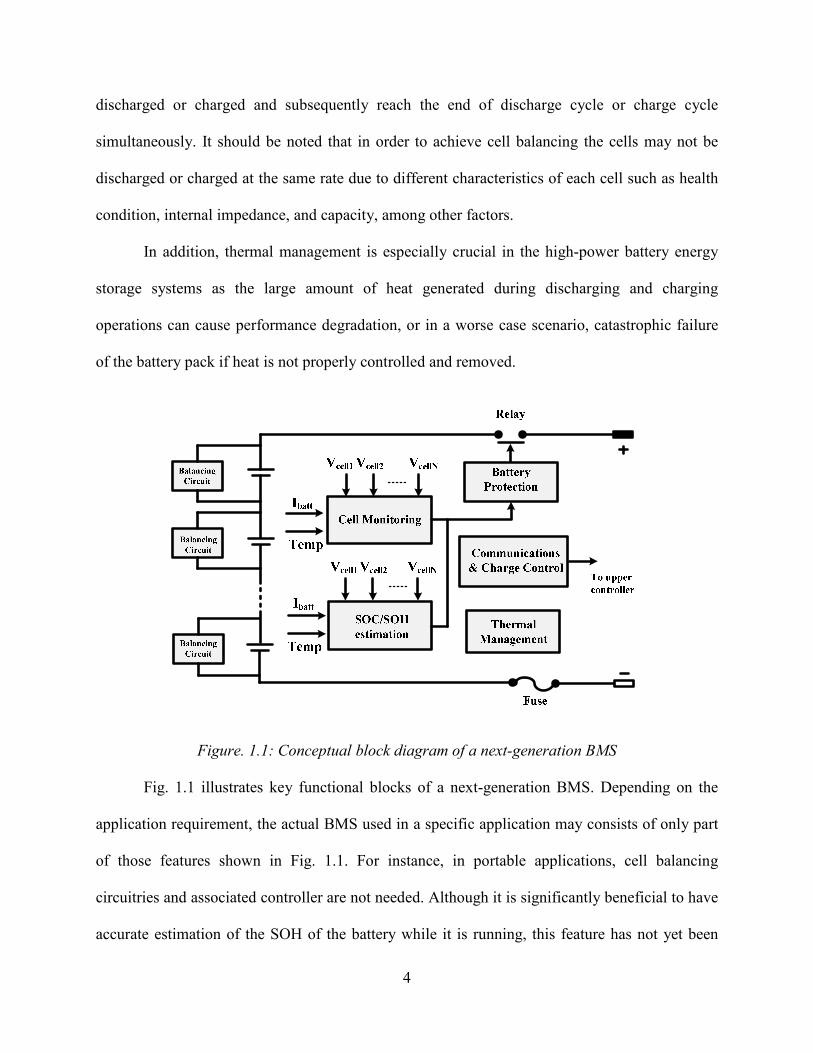
of the battery pack if heat is not properly controlled and removed.
Figure. 1.1: Conceptual block diagram of a next-generation BMS
Fig. 1.1 illustrates key functional blocks of a next-generation BMS. Depending on the
application requirement, the actual BMS used in a specific application may consists of only part
of those features shown in Fig. 1.1. For instance, in portable applications, cell balancing
circuitries and associated controller are not needed. Although it is significantly beneficial to have
accurate estimation of the SOH of the battery while it is running, this feature has not yet been
5
fully demystified, and therefore, has not been extensively applied to the practical battery system
applications due to the complexity of the factors which can impact the SOH of the battery. Each
of the functional blocks shown in Fig. 1.1 are introduced in the following subsections.
A. Battery Pack/Cell(s)
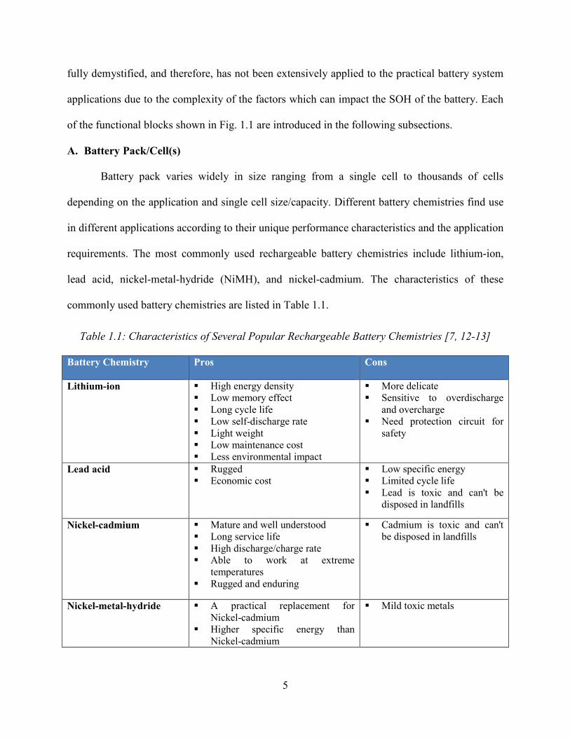
Battery pack varies widely in size ranging from a single cell to thousands of cells
depending on the application and single cell size/capacity. Different battery chemistries find use
in different applications according to their unique performance characteristics and the application
requirements. The most commonly used rechargeable battery chemistries include lithium-ion,
lead acid, nickel-metal-hydride (NiMH), and nickel-cadmium. The characteristics of these
commonly used battery chemistries are listed in Table 1.1.
Table 1.1: Characteristics of Several Popular Rechargeable Battery Chemistries [7, 12-13]
Battery Chemistry Pros Cons
Lithium-ion High energy density Low memory effect Long cycle life Low self-discharge rate Light weight Low maintenance cost Less environmental impact
More delicate Sensitive to overdischarge
and overcharge Need protection circuit for
safety
Lead acid Rugged Economic cost
Low specific energy Limited cycle life Lead is toxic and can't be
disposed in landfills
Nickel-cadmium Mature and well understood Long service life High discharge/charge rate Able to work at extreme
temperatures Rugged and enduring
Cadmium is toxic and can't be disposed in landfills
Nickel-metal-hydride A practical replacement for Nickel-cadmium
Higher specific energy than Nickel-cadmium
Mild toxic metals

6
Due to the advantages including high energy density, long cycle life, low memory effect,
less environmental impact, and low self-discharge rate, lithium-ion chemistry has received the
most significant attention in the past decade and become increasingly popular in portable
electronics, EVs/PHEVs, and distributed microgrids energy storage applications. The lithium-ion
family of batteries has been gradually replacing the nickel and lead-acid based chemistries which
has dominated the battery world until the 1990s [12-13].
B. Cell Monitoring and Protection
Voltage, current and temperature of each cell in the battery pack are constantly monitored
for various purposes including
1) Protect the cell from overdischarge and overcharge which is hazardous to the cell,
especially for lithium-ion chemistry
2) Protect the cell from being discharged/charged at excessive rates which can greatly
shorten the usable capacity and cycle life of the cell
3) Maintain appropriate operating temperature range to optimize battery performance
4) Provide voltage, current and temperature inputs to the SOC and/or SOH estimation
algorithms
C. State-of-Charge Estimation
State-of-charge (SOC) is one of the most important state indicators for the battery. It is
generally defined as the ratio of the amount of charges remaining in the battery (Qr) to the total
amount of charges (Qf) when the battery is fully charged, as given by
678 = :;:< (1.1)
7
In other words, SOC indicates the amount of electrical energy the battery is able to
supply before it is depleted. The purposes of battery SOC estimation include but are not limited
to the following:
1. Avoid overdischarging/overcharging of the battery
2. User convenience
3. Required for cell balancing
A variety of approaches have been proposed in the literature as those presented in [12-18]
to estimate the SOC of the battery. These SOC estimation methods can be classified into the
following categories:
1) Coulomb counting method [12]. By integrating the current flowing in and out of the battery
over time, the amount of charges available in the battery can be estimated. Despite its
simplicity, the coulomb counting method does not take into account some key factors that
can affect the accuracy of SOC estimation, such as the temperature variation,
charge/discharge rate and battery aging effect. Moreover, the coulomb counting method is
sensitive to the accuracy of the initial current value and current measurement.
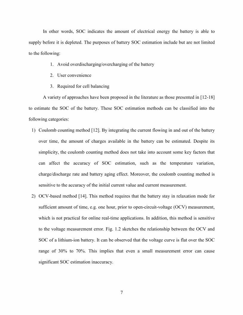
2) OCV-based method [14]. This method requires that the battery stay in relaxation mode for
sufficient amount of time, e.g. one hour, prior to open-circuit-voltage (OCV) measurement,
which is not practical for online real-time applications. In addition, this method is sensitive
to the voltage measurement error. Fig. 1.2 sketches the relationship between the OCV and
SOC of a lithium-ion battery. It can be observed that the voltage curve is flat over the SOC
range of 30% to 70%. This implies that even a small measurement error can cause
significant SOC estimation inaccuracy.
8
Figure. 1.2. A sketch of OCV vs. SOC for a lithium-ion battery
3) Electrochemical model-based methods [18]. Despite their accuracy, this type of methods
generally are based on solving the detailed nonlinear differential equations which describe
the electrochemical behavior of the battery. This requires significant computational
resources, and therefore, are not suited for online real-time applications.
4) Electrical circuit model-based methods [19-22]. This type of methods require electrical
battery models which characterize electrochemical behavior and dynamics of the battery.
Adaptive and non-linear techniques, such as extended Kalman filter and sliding-mode
observer, can be used to improve the accuracy of the electrical circuit models. However,
these techniques would increase the complexity of implementation. Moreover, the
estimation error could be large due to the noise present in the system.
5) Computational intelligence-based methods, such as artificial neural network (ANN), fuzzy
logic method and support vector regression methods [23-25]. The disadvantage of this type
of methods is the need for learning/training process with a large amount of prior
data/knowledge.
9
D. State-of-Health Estimation
State-of-health (SOH) is another important state indicator for the battery. Unfortunately,
there has been no established definition of the SOH. In some literature [20, 23, 26], SOH is
defined as the ratio of the present usable/available capacity (8=) to the rated capacity of the
battery (8), as given by
67> = '?'; (2)
SOH can be used as a measure of the health condition of the battery and its ability to
deliver specified performance compared with a fresh battery. Like human being, the health
condition of the battery tends to deteriorate over time due to irreversible physical and chemical
changes occurring with usage [13].
In general, capacity and impedance variation of the battery are regarded as the leading
indicators of the SOH of the battery [15-16, 20, 23, 26]. Unlike the estimation of the SOC, SOH
estimation does not usually have stringent requirement of the tracking/estimation speed due to
much slower dynamics associated with the variation of the SOH. Several SOH estimation
methods have been presented in the literature, the majority of which fall into two categories, i.e.,
capacity estimation and computational intelligence-based techniques [27-30].
AC battery impedance data have been shown to be effective in reflecting variations in the
electrochemical processes which reveal the changes taking place in the battery electrode surface
and diffusion layer [31]. Therefore, AC impedance of the battery can potentially be utilized as an
effective tool for assessing the health condition of the battery, as will be discussed in details later
in this chapter.
E. Battery Modeling
10
A model which represents the electrochemical characteristics and dynamics of the battery
is essential for the states (e.g., SOC and SOH) estimation, circuit simulation and analysis, and
battery design and characterization. A wide variety of battery models have been presented in the
literature [18-20, 26-31]. These models have varying degrees of complexity and accuracy. In
general, these models fall under three categories, i.e., electrochemical models, analytical models
and electrical circuit models.
As mentioned earlier, electrochemical models are based on detailed nonlinear differential
equations which describe the chemical reactions that occur inside the battery. Despite their high
accuracy, these models do not usually find practical use in real-time applications due to the need
of detailed knowledge of the battery chemical processes and much computational resources.
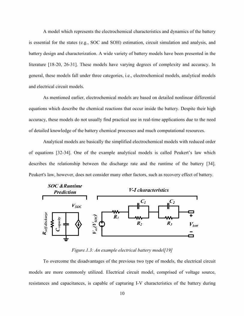
Analytical models are basically the simplified electrochemical models with reduced order
of equations [32-34]. One of the example analytical models is called Peukert’s law which
describes the relationship between the discharge rate and the runtime of the battery [34].
Peukert's law, however, does not consider many other factors, such as recovery effect of battery.
Figure.1.3: An example electrical battery model[19]
To overcome the disadvantages of the previous two type of models, the electrical circuit
models are more commonly utilized. Electrical circuit model, comprised of voltage source,
resistances and capacitances, is capable of capturing I-V characteristics of the battery during
11
discharging and charging operation. Fig. 1.3. shows an example electrical circuit battery model
[19]. By identifying the RC parameters of the model based on the measured voltage, current and
temperature information, the SOC and SOH of the battery can be estimated in real time. There
are some other battery models which combine the analytical model and electrical circuit model,
as the one presented in the literature [20].
F. Cell Balancing
In multi-cell battery systems, in order to ensure charge balance between the battery cells
during discharging and charging operation, cell balancing circuits and controls are needed as an
integral part of the BMS. More details regarding the cell balancing will be available later in this
chapter.
G. Charge Control
Different battery packs have different charge rate limit depending on the chemistry,
capacity and series/parallel configuration of the cells being used. The objective is to achieve
highest possible charging speed without compromising the charging efficiency, safety and life of
the battery. This would require coordination of BMS and battery charge controller [40-41].
H. Thermal Management
The chemical reactions that occur inside the battery is dependent on temperature. The
nominal battery performance is generally specified over a temperature range which may vary by
applications. Operating at high and low temperatures can cause the battery performance to
deviate from the nominal performance. For instance, operating at low temperature results in
lower usable capacity of the battery. Therefore, thermal management is necessary for the battery
system in order to deliver its specified performance. By performing heat-transfer analysis of the
12
battery pack based on its cell chemistry and architecture, liquid or air cooling can be used to
remove the heat.
I. Communication
Communication is another important building block of the BMS functions. For example
in the EVs/PHEVs applications, the BMS is usually coupled to other vehicle systems which
communicate with the BMS via CAN communication interface. In some cases, there may also be
system programming, monitoring and data logging requirements using RS232 series bus [13].
1.3 Battery Impedance Measurement
While the battery can be electrically modeled as a combination of voltage source,
capacitors and resistors, it is a challenging task to accurately identify each of the model
parameters which adaptively vary with many factors in real time, such as SOC, temperature,
discharge/charge rate. Impedance, as a lumped representation of the RC network in the model,
can be a effective tool to reveal the electrochemical characteristics of the battery. The impedance
of the battery provides useful information on the performance of the battery and can also help to
detect trouble spots hidden in the battery since the degradation of electrodes and electrolyte
should be reflected in the variation of the impedance [12-13]. The battery impedance variations
across different frequency ranges are revealed to be directly correlated to the health condition of
the battery [15, 30-31]. Therefore, battery impedance measurement can potentially be used as an
effective tool to assess the SOH of the battery.
The battery AC impedance spectroscopy can also be used to estimate the SOC of the
battery by comparing the measured electrochemical impedance spectrum against the long-term
experimental data collected across the full SOC range [15].
13
Offline battery impedance measurement methods, such as electrochemical impedance
spectroscopy (EIS), has been extensively studied in the literature [28-31]. In EIS, a small charge
neutral AC voltage/current signal is applied to the battery and the current/voltage response of the
battery is captured to determine the impedance of the battery at a given frequency. A frequency
sweep over a specified frequency range is performed in order to draw an impedance spectrum of
the battery. Since the EIS measurement are performed sequentially, it can take a long period of
time to complete, which make it not ideal for online real-time applications such as EVs/PHEVs
and smart grids. In addition, EIS measurements require extra signal injection circuit/hardware.
For these reasons, EIS measurement is generally limited to lab characterization and testing.
Despite rapidly growing demands in real-time applications, online fast battery impedance
measurement has not been discussed extensively in the literature. A method named "Harmonic
Compensated Synchronous Detection (HCSD)" is presented in [31] where an AC current signal
composed of a sum of sinusoidal waves with a range of frequencies is injected to the battery. The
impedance of the battery at each frequency of interest is then determined simultaneously. The
duration of a complete measurement cycle can be reduced to a period of the lowest injected
frequency. However, this method still requires signal injection through external circuits.
Moreover, this method have only been tested under the scenario where the battery is directly
connected to an emulated load. This rarely is the case in practical online applications where the
battery typically is interfaced to the load via a DC-DC switching power converter in order to
provide necessary voltage/current regulation. The transfer function and impedance of the power
converter or power system may impact the accuracy of the impedance measurement with the
HCSD method.
14
One of the major focuses of this dissertation work is on proposing and developing a true
online battery impedance measurement method. In the proposed method, instead of injecting AC
signal through external generator, the duty cycle value of the DC-DC power converter that
interfaces the battery to the load is perturbed in a sinusoidal manner at a given frequency around
its steady-state DC value. The resulted sinusoidal ripples of the battery voltage and battery
current are measured in order to determine the AC impedance of the battery at the perturbation
frequency. The proposed method can be performed either continuously or periodically without
interrupting the normal operation of the battery system and DC-DC power converter. This work
also provides an example where the obtained impedance data is utilized for online SOC
estimation of lithium-ion batteries.
1.4 Cell Balancing
The second focus of this dissertation work is on cell balancing. As briefly introduced
earlier in this chapter, cell balancing circuits and associated controller can be implemented as an
integral part of the battery management system (BMS) in order to ensure uniform
discharging/charging between the battery cells.
A wide variety of cell balancing methods have been presented in the literature which will
be reviewed and discussed in details in chapter 3. In general, the cell balancing methods fall into
two main categories: passive (dissipative) and active (energy-recovery) cell balancing schemes.
Passive cell balancing schemes basically dissipate the excess energy of the cells that have higher
SOC values in the form of heat. On the other hand, active cell balancing methods achieve cell
balancing by transferring/redistributing the excess energy between the battery cells or between
the cells and the pack. Therefore, active cell balancing schemes generally are more efficient but
more costly and complex to implement than passive cell balancing schemes.
15
In this dissertation work, the cell imbalance issue is addressed from a totally different
perspective than existing solutions. An energy sharing based cell balancing control scheme is
proposed for a distributed battery energy storage system architecture. Instead of treating the cell
balancing system and DC bus voltage regulation system as two independent systems, the
proposed distributed battery system architecture with energy sharing controller combines these
two systems into a single system. The re-designed DC-DC power stage with the proposed energy
sharing controller is utilized to achieve SOC balancing between the battery cells and DC bus
voltage regulation at the same time. The cells' SOC imbalance issue is addressed from the root
by using the energy sharing control concept to automatically adjust the discharge/charge rate of
each battery cell while maintaining total regulated DC bus voltage. The energy transfer between
the battery cells which is usually required in the conventional cell balancing schemes is no
longer needed. As a result, the power losses along the energy transfer path are eliminated. Due to
the difference in the nature of discharging and charging operation, the energy sharing controller
design and implementation are different in discharge and charge mode.
1.5 Cross Regulation of Single-Inductor Multiple-Output DC-DC Switching Converters
Single-Inductor Multiple-Output (SIMO) DC-DC switching converter is a cost-effective
alternative to multiple-individual-switching-converter architecture in many applications such as
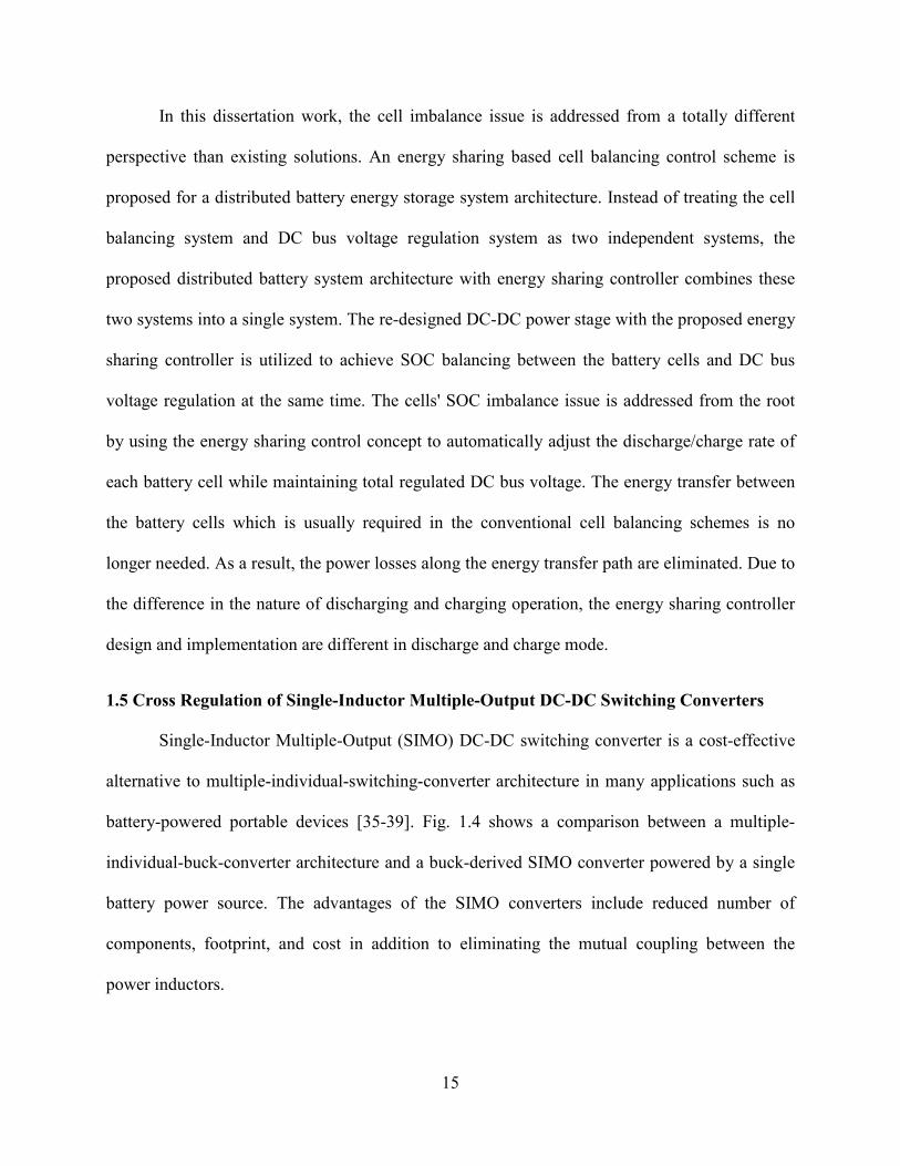
battery-powered portable devices [35-39]. Fig. 1.4 shows a comparison between a multiple-
individual-buck-converter architecture and a buck-derived SIMO converter powered by a single
battery power source. The advantages of the SIMO converters include reduced number of
components, footprint, and cost in addition to eliminating the mutual coupling between the
power inductors.
16
(a) (b)
Figure. 1.4: Circuit diagram of (a) multiple switching DC-DC power converter architecture (b)
single-input multiple-output switching DC-DC power conerter architecture
However, due to the fact that the multiple output voltage rails are coupled to the same
switching node in a SIMO converter, the cross regulation between the outputs can severely
degrade the output voltage regulation performance during steady-state and dynamic operations
and may even cause system instability in a worst case scenario. To address this issue, this
dissertation work proposes a new control scheme called power-multiplexed control (PM control).
By operating the output switches at a lower frequency than the power stage switches, each output
is independently regulated when the corresponding output switch is turned on. This PM control
scheme completely eliminates the cross regulation between the outputs under both steady-state
and dynamic operations regardless of the operating mode, i.e., CCM (continuous conduction
mode) or DCM (discontinuous conduction mode).
17
1.6 Dissertation Outline
Next chapter presents an online battery impedance measurement method. The theoretical
basis of the proposed method is first introduced followed by implementation details of each
block of the digital controller. The experimental results are then presented to validate the
proposed method. An example is also provided at the end of Chapter 2 where the obtained
impedance data are used to estimate the SOC of a lithium-ion battery.
Chapter 3 presents an energy sharing controller based on a distributed battery energy
storage system architecture which results in achieving cell balancing between the battery cells
while regulating the DC bus voltage during discharging operation. The distributed battery system
architecture is first introduced and compared against the conventional centralized architecture in
terms of structure, operation, control strategy, among others. Then the operation of the proposed
energy sharing controller is introduced and discussed in details in the context of discharging
operation. The steady-state analysis of the distributed battery system with the energy sharing
controller is also presented in this chapter. The operation and design of each control loop are
covered in Chapter 3. Experimental results are presented in the last section of Chapter 3 to
demonstrate the effectiveness and feasibility of the proposed concept.
Since the battery charging operation is quite different than discharging operation by
nature, the energy sharing controller proposed in Chapter 3 is upgraded by integrating the energy
sharing control concept with a battery charging control algorithm in order to achieve cell
balancing while the battery is being charged. The principle of operation of different control
loops, including SOC balancing, BPM converter input voltage regulation and average cell
current/voltage control loops, are discussed in details in Chapter 4. The experimental results for
both constant current charging mode (CCCM) and constant voltage charging mode (CVCM)

18
operation are also given for verification. At the end of Chapter 4, several comments are made
regarding the energy sharing controlled distributed battery system in terms of the size, cost,
efficiency.
In order to understand the dynamics and provide insights to the energy sharing control
loop design, small-signal modeling and analysis of the energy sharing controlled distributed
battery system is performed and presented in Chapter 5. The small-signal models are constructed
and associated transfer functions are derived for different operating modes including discharging,
constant current charging and constant voltage charging mode. Based on the derived small signal
models, the control loops are compensated by using the rule-of-thumb frequency-domain design
guidelines. Simulation and experimental validation are conducted on a two-cell distributed
battery system prototype to prove the effectiveness of the derived small signal models and
designed compensators.
Chapter 6 presents the PM control for SIMO converters in order to eliminate the cross
regulation between the outputs of a SIMO converter. The architecture of the SIMO topology and
the basic operation principle of the PM control scheme are first presented and discussed. The
steady-state operation analysis of the PM controlled SIMO converter during both DCM and
CCM operations are also presented. Experimental results obtained from a two-output buck SIMO
converter prototype are presented and discussed to verify the proposed concept .
The last chapter summarizes and concludes this dissertation research work in addition to
giving some directions for future work.
19
CHAPTER 2
ONLINE BATTERY IMPEDANCE MEASUREMENT METHOD
2.1 Introduction
The electrochemical batteries have been extensively used for energy storage and supply
in industrial, telecommunications, medical, electric utility, consumer and portable electronics
applications [1-5, 1-7]. In the past decade, a variety of emerging applications that require
batteries have received significant attentions including portable electronics (e.g. smart phones
and tablets), EVs and smart grids. The battery energy storage system plays a key role in such
applications because it can significantly impact the performance, life, cost, reliability and safety
of such systems. While rapid progress has been made in terms of the battery technologies, few
transformative advances have emerged in regard to the BMS that is needed to ensure efficient,
safe and robust operation of the battery pack [7].
A state-of-the-art BMS typically implements various functions and capabilities including
cell-level voltage, current and temperature monitoring and protection, battery pack prognosis and
diagnosis, state of charge (SOC) estimation and state of health (SOH) estimation, cell balancing,
and/or communications, among others [14-17, 27-30, 44-50]. The impedance of the battery is an
important parameter because it provides useful information on the performance of the battery
and can also help to detect trouble spots hidden in the battery system [15-17, 27-30, 44-50].
To achieve efficient power and energy management of the battery system, accurate SOC
information of the battery is needed as a measure of the electrical energy remaining in the
battery. Several SOC estimation methods have been proposed as in the literature [15-17, 27, 48-
50, 57]. Some of the commonly used methods have been reviewed and compared in Chapter 1.
20
Among these methods, battery impedance based approaches can potentially result in higher
accuracy of estimation as the impedance itself already takes into account several factors, such as
capacity variation and temperature variation, which are usually neglected in other methods.
As the battery ages, the impedance of the battery tends to increase. Comparing the actual
impedance with either the impedance when the battery was new or a reference impedance value
that is set based on long-term experimental data can be utilized as a measure of the SOH of the
battery [29]. AC impedance spectroscopy method [15-16, 30, 44, 46-47] can also be used to
estimate the SOH of the battery based on analyzing the impedance spectra.
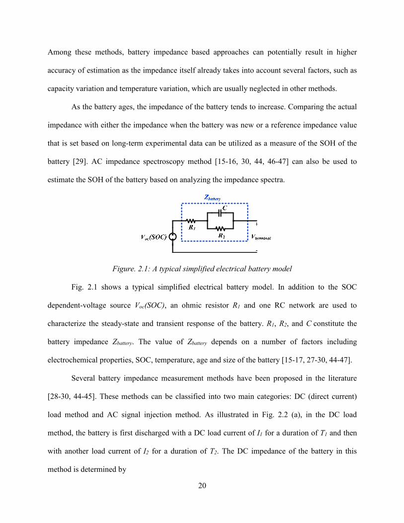
Figure. 2.1: A typical simplified electrical battery model
Fig. 2.1 shows a typical simplified electrical battery model. In addition to the SOC
dependent-voltage source Voc(SOC), an ohmic resistor R1 and one RC network are used to
characterize the steady-state and transient response of the battery. R1, R2, and C constitute the
battery impedance Zbattery. The value of Zbattery depends on a number of factors including
electrochemical properties, SOC, temperature, age and size of the battery [15-17, 27-30, 44-47].
Several battery impedance measurement methods have been proposed in the literature
[28-30, 44-45]. These methods can be classified into two main categories: DC (direct current)
load method and AC signal injection method. As illustrated in Fig. 2.2 (a), in the DC load
method, the battery is first discharged with a DC load current of I1 for a duration of T1 and then
with another load current of I2 for a duration of T2. The DC impedance of the battery in this
method is determined by
21
1 2
_
2 1
battery dc
V Vz
I I
−=− (2.1)
where V1 and V2 are the terminal voltages of the battery under DC load current values of I1 and
I2, respectively. As the name suggests, the DC load method yields only the ohmic DC resistance
value of the battery.
Battery
+
-
V
(a) (b)
Figure. 2.2: (a) Circuit diagram of DC load impedance measurement method; (b) Circuit
diagram of AC signal injection impedance measurement method
On the other hand, the AC signal injection method is more often used for AC impedance
measurement of the battery. The basic idea of the AC signal injection method is to excite the
battery with a small AC sinusoidal current/voltage signal at a given frequency f , as illustrated in
Fig. 2.2 (b), and then measuring the AC voltage/current response of the battery to the injected
AC current/voltage signal in order to determine the AC impedance of the battery by using (2.2).
( ) zjac
batteryac
Vz f e
I
ϕ= (2.2)
where Vac and Iac are the amplitudes of the AC component of the battery voltage and battery
current, respectively, and zϕ is the phase of the battery impedance. The AC signal injection
method is relatively complicated and costly due to the need for extra devices/circuitries to
generate the required AC excitation signal and to measure the response.
22
Moreover, in what is referred to in the literature as “online impedance measurement”
methods [28-30, 44-46], the battery under test is typically directly connected to an emulated
constant current or constant resistive load (e.g. using a commercial battery tester), as illustrated
in Fig. 2.2 (a) and (b), instead of being connected to an actual running system. In the latter case,
a power converter is usually used to interface the battery with the load in order to provide
necessary voltage/current regulation. Therefore, the transfer function and impedance of the
power converter or power system, which is connected to the battery, might impact the accuracy
of impedance measurement, which has not been discussed clearly in the literature [28-30, 44-45].
Other potential issues include system instability, interruption of the power converter normal
operation, and/or noise and disturbance from the injected AC signal.
In this chapter, a true “online” battery impedance measurement method is first proposed.
The term “online” here refers to the fact that the battery impedance measurement is performed
during system operation. In the proposed method, instead of injecting AC signal through external
generator, the duty cycle value of the DC-DC power converter, which is used to interface the
battery with the load, is perturbed in a sinusoidal fashion at a given frequency around its steady
state DC value (the duty cycle value needed to achieve a desired output voltage regulation). This
duty cycle perturbation results in sinusoidal variations of the battery voltage and battery current
around their corresponding steady-state DC values. The sinusoidal ripples of the battery voltage
and battery current are then measured and used to determine the AC impedance of the battery at
the perturbation frequency. The proposed method can be performed either continuously or
periodically without interrupting the normal operation of the battery system and the power
converter. Moreover, this chapter provides an example where the obtained impedance data is
used for online SOC estimation of lithium-ion batteries.
23
The remainder of this chapter is organized as follows: the principle of operation of the
basic online impedance measurement method is introduced and the implementation details are
discussed in Section II. Section III presents the proof-of-concept experimental prototype results
and discussion.
2.2 Online Battery Impedance Measurement
As mentioned earlier, in the battery-powered devices or systems, a DC-DC power
converter is usually used to interface the battery with the load in order to provide voltage/current
regulation. In many applications, this DC-DC power converter is usually bidirectional in order to
allow for both charge and discharge operations of the battery system. A variety of DC-DC power
converter topologies are available and the choice of the topology is mainly a function of target
power level, power density, size and cost requirements, as well as integration and packaging
simplicity for a given application.
A conventional non-isolated bidirectional DC-DC boost/buck converter, as shown in Fig.
2.3, is utilized in this work for illustration and validation. This bidirectional DC-DC power
converter operates as a boost converter during discharge mode in order to step up the voltage to
the voltage level required by the load and operates as a buck converter in battery charge mode in
order to step down the voltage to the battery voltage.
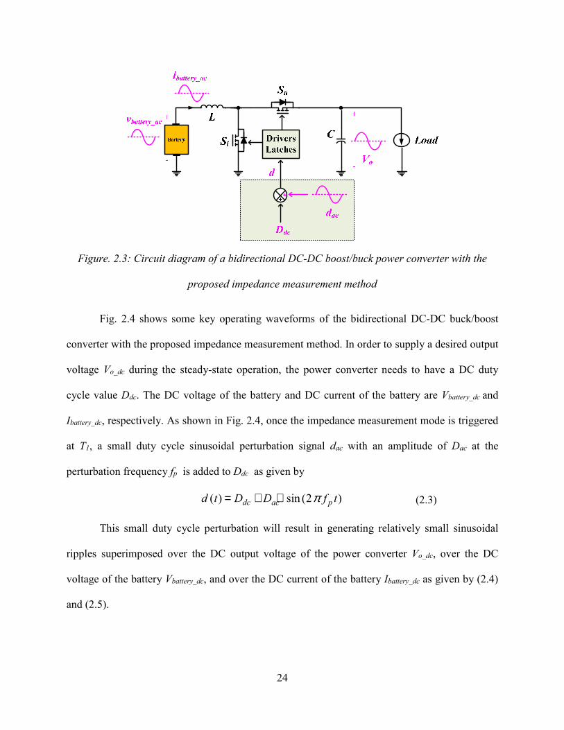
24
Figure. 2.3: Circuit diagram of a bidirectional DC-DC boost/buck power converter with the
proposed impedance measurement method
Fig. 2.4 shows some key operating waveforms of the bidirectional DC-DC buck/boost
converter with the proposed impedance measurement method. In order to supply a desired output
voltage Vo_dc during the steady-state operation, the power converter needs to have a DC duty
cycle value Ddc. The DC voltage of the battery and DC current of the battery are Vbattery_dc and
Ibattery_dc, respectively. As shown in Fig. 2.4, once the impedance measurement mode is triggered
at T1, a small duty cycle sinusoidal perturbation signal dac with an amplitude of Dac at the
perturbation frequency fp is added to Ddc as given by
( ) sin (2 )dc ac pd t D D f tπ= + ⋅ (2.3)
This small duty cycle perturbation will result in generating relatively small sinusoidal
ripples superimposed over the DC output voltage of the power converter Vo_dc, over the DC
voltage of the battery Vbattery_dc, and over the DC current of the battery Ibattery_dc as given by (2.4)
and (2.5).
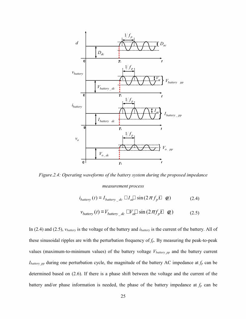
25
batteryi
d
batteryv
ov
dcD
_battery dcV
_battery dcI
_o dcV
acD
_battery ppV
_battery ppI
_o ppV
1 pf
1 pf
1 pf
1 pf
acV
acI
Figure.2.4: Operating waveforms of the battery system during the proposed impedance
measurement process
_( ) sin (2 )battery battery dc ac p ii t I I f tπ φ= + ⋅ + (2.4)
_( ) sin (2 )battery battery dc ac p vv t V V f tπ φ= + ⋅ + (2.5)
In (2.4) and (2.5), vbattery is the voltage of the battery and ibattery is the current of the battery. All of
these sinusoidal ripples are with the perturbation frequency of fp. By measuring the peak-to-peak
values (maximum-to-minimum values) of the battery voltage Vbattery_pp and the battery current
Ibattery_pp during one perturbation cycle, the magnitude of the battery AC impedance at fp can be
determined based on (2.6). If there is a phase shift between the voltage and the current of the
battery and/or phase information is needed, the phase of the battery impedance at fp can be
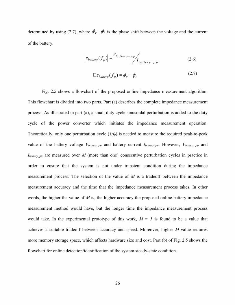
26
determined by using (2.7), where v iϕ ϕ− is the phase shift between the voltage and the current
of the battery.
( ) bat ter y p pbattery p
batter y p p
Vz f
I−
−= (2.6)
( )battery p v iz f ϕ ϕ∠ = − (2.7)
Fig. 2.5 shows a flowchart of the proposed online impedance measurement algorithm.
This flowchart is divided into two parts. Part (a) describes the complete impedance measurement
process. As illustrated in part (a), a small duty cycle sinusoidal perturbation is added to the duty
cycle of the power converter which initiates the impedance measurement operation.
Theoretically, only one perturbation cycle (1/fp) is needed to measure the required peak-to-peak
value of the battery voltage Vbattery_pp and battery current Ibattery_pp. However, Vbattery_pp and
Ibattery_pp are measured over M (more than one) consecutive perturbation cycles in practice in
order to ensure that the system is not under transient condition during the impedance
measurement process. The selection of the value of M is a tradeoff between the impedance
measurement accuracy and the time that the impedance measurement process takes. In other
words, the higher the value of M is, the higher accuracy the proposed online battery impedance
measurement method would have, but the longer time the impedance measurement process
would take. In the experimental prototype of this work, M = 5 is found to be a value that
achieves a suitable tradeoff between accuracy and speed. Moreover, higher M value requires
more memory storage space, which affects hardware size and cost. Part (b) of Fig. 2.5 shows the
flowchart for online detection/identification of the system steady-state condition.
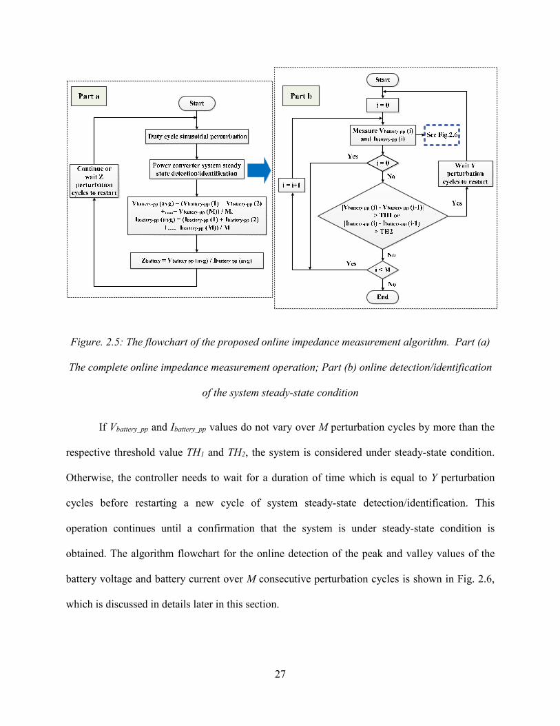
27
Figure. 2.5: The flowchart of the proposed online impedance measurement algorithm. Part (a)
The complete online impedance measurement operation; Part (b) online detection/identification
of the system steady-state condition
If Vbattery_pp and Ibattery_pp values do not vary over M perturbation cycles by more than the
respective threshold value TH1 and TH2, the system is considered under steady-state condition.
Otherwise, the controller needs to wait for a duration of time which is equal to Y perturbation
cycles before restarting a new cycle of system steady-state detection/identification. This
operation continues until a confirmation that the system is under steady-state condition is
obtained. The algorithm flowchart for the online detection of the peak and valley values of the
battery voltage and battery current over M consecutive perturbation cycles is shown in Fig. 2.6,
which is discussed in details later in this section.
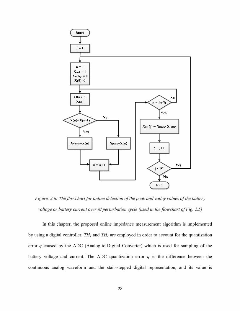
28
Figure. 2.6: The flowchart for online detection of the peak and valley values of the battery
voltage or battery current over M perturbation cycle (used in the flowchart of Fig. 2.5)
In this chapter, the proposed online impedance measurement algorithm is implemented
by using a digital controller. TH1 and TH2 are employed in order to account for the quantization
error q caused by the ADC (Analog-to-Digital Converter) which is used for sampling of the
battery voltage and current. The ADC quantization error q is the difference between the
continuous analog waveform and the stair-stepped digital representation, and its value is
29
uniformly distributed between -0.5×LSB and +0.5×LSB (LSB stands for Least Significant Bit of
the digital/binary number) as given by
0.5 0.5LSB q LSB− ⋅ ≤ ≤ + ⋅ (2.8)
The value of LSB is equal to the resolution of the ADC, Vrange/2N , where Vrange is the full
scale input analog voltage range of the ADC, and N is the number of bits (number of bits in the
digital number or word) of the ADC. Therefore, the maximum quantization error maxq for battery
voltage/current sampling can be expressed as
max / (2 2 )Nrangeq V= ⋅
(2.9)
Since the peak-to-peak value Vbattery_pp (or Ibattery_pp) is obtained by subtracting the
maximum value and the minimum value of vbattery (or ibattery), there is a maximum quantization
error in the worst case scenario in the calculation of Vbattery_pp (or Ibattery_pp) which equals twice
the quantization error given by (2.9). This maximum quantization error (qpp_max) is given by
_ max / 2Npp rangeq V= (2.10)
Based on this, TH1 and TH2 threshold values are defined as given by (2.11) and (2.12).
TH1 (for Vbattery_pp) and TH2 (for Ibattery_pp) are used in the algorithm in order to account for the
quantization error caused by the finite ADC resolution.
1
1 1 / 2NrangeTH V= (2.11)
2
2 2 / 2NrangeTH V= (2.12)
where Vrange1 is the full scale input analog voltage range of the ADC that is used to sample the
battery voltage, N1 is the number of bits of the ADC that is used to sample the battery voltage.
30
Vrange2 is the full scale input analog voltage range of the ADC that is used to sample the battery
current, and N2 is the number of bits of the ADC that is used to sample the battery current.
If the change in Vbattery_pp (or Ibattery_pp) values over M consecutive perturbation cycles is
less than TH1 (or TH2), then the system can be considered under steady-state condition.
Otherwise, the system is considered under transient condition and another cycle of system
steady-state detection/identification will need to be started after a duration of time that is equal to
Y perturbation cycles.
As soon as the system steady-state condition status is confirmed, the Vbattery_pp and
Ibattery_pp values over M consecutive perturbation cycles are averaged and used to determine the
magnitude of the battery AC impedance based on (2.6). The proposed impedance measurement
method can either be performed continuously or periodically by waiting Z perturbation cycles
before restarting a new cycle of impedance measurement.
If there is a phase shift between the voltage and the current of the battery and it is desired
to obtain the information of this phase shift as in (2.7), the time delay (td) between the peak of
the battery voltage and the peak of the battery current is recorded in the digital controller. Then,
the phase can be obtained by
360 / (1/ ) 360v i d p d pt f t fϕ ϕ− = ⋅ = ⋅ ⋅o o (2.13)
Fig. 2.6 shows the flowchart for online detection of the peak and valley values of the
battery voltage or battery current over M perturbation cycles. X represents the battery voltage or
battery current signal. A counter is used to count the number of switching cycles, and the initial
value n of this counter is set to 1. Another counter is used to count the number of perturbation
cycles, and the initial value j of this counter is also set to 1. One value of the signal X is obtained
31
per switching cycle, and therefore, the number of signal values obtained per perturbation cycle is
equal to fsw/fp. As the value of n increases, if the value of X, i.e., X(n), is less than its previous
value X(n-1), then this value is recorded as the current valley value in the Xvalley register.
Otherwise, this value is recorded as the current peak value in the Xpeak register. When n reaches a
value that is equal to fsw/fp indicating that a full perturbation cycle sampling and detection is
completed, the values recorded in the Xpeak and Xvalley registers are the peak value and the valley
value of the signal for this perturbation cycle, respectively. This operation continues for M
perturbation cycles. Note that the ADC sampling rate of the signal can be set equal to the
switching frequency (fsw) and in this case only one ADC sample is used to obtain one value of
the signal X per switching cycle. In order to minimize the error and achieve higher accuracy, the
sampling rate of the ADC can be set higher than the switching frequency and multiple ADC
samples per switching cycle (i.e., oversampling) are averaged in order to obtain one value of the
signal X per switching cycle. This one value per switching cycle is what is needed in the
flowchart of Fig. 2.6.
Measuring the DC impedance value by using the proposed method that utilizes the duty
cycle perturbation of the power converter is relatively simple. Two values for the voltage of the
battery (V1 and V2) and two values for the current of the battery (I1 and I2) are obtained for two
duty cycle values (D1 and D2), respectively. Then the DC impedance can be calculated by
1 2
_
2 1
battery dc
V Vz
I I
−=− (2.14)
2.3 Proof-of-Concept Experimental Results
A proof-of-concept experimental laboratory prototype is built in order to validate the
proposed online impedance measurement method and its utilization in an example online SOC
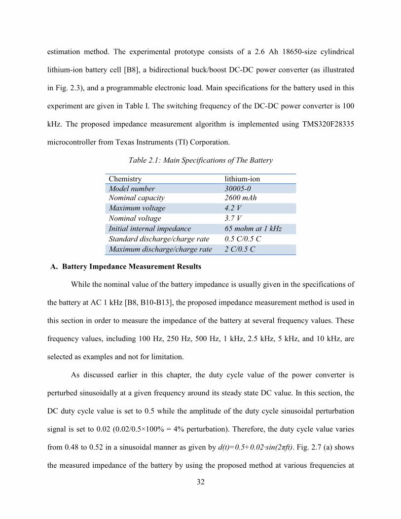
32
estimation method. The experimental prototype consists of a 2.6 Ah 18650-size cylindrical
lithium-ion battery cell [B8], a bidirectional buck/boost DC-DC power converter (as illustrated
in Fig. 2.3), and a programmable electronic load. Main specifications for the battery used in this
experiment are given in Table I. The switching frequency of the DC-DC power converter is 100
kHz. The proposed impedance measurement algorithm is implemented using TMS320F28335
microcontroller from Texas Instruments (TI) Corporation.
Table 2.1: Main Specifications of The Battery
Chemistry lithium-ion
Model number 30005-0
Nominal capacity 2600 mAh
Maximum voltage 4.2 V
Nominal voltage 3.7 V
Initial internal impedance 65 mohm at 1 kHz
Standard discharge/charge rate 0.5 C/0.5 C
Maximum discharge/charge rate 2 C/0.5 C
A. Battery Impedance Measurement Results
While the nominal value of the battery impedance is usually given in the specifications of
the battery at AC 1 kHz [B8, B10-B13], the proposed impedance measurement method is used in
this section in order to measure the impedance of the battery at several frequency values. These
frequency values, including 100 Hz, 250 Hz, 500 Hz, 1 kHz, 2.5 kHz, 5 kHz, and 10 kHz, are
selected as examples and not for limitation.
As discussed earlier in this chapter, the duty cycle value of the power converter is
perturbed sinusoidally at a given frequency around its steady state DC value. In this section, the
DC duty cycle value is set to 0.5 while the amplitude of the duty cycle sinusoidal perturbation
signal is set to 0.02 (0.02/0.5×100% = 4% perturbation). Therefore, the duty cycle value varies
from 0.48 to 0.52 in a sinusoidal manner as given by d(t)=0.5+0.02·sin(2πft). Fig. 2.7 (a) shows
the measured impedance of the battery by using the proposed method at various frequencies at
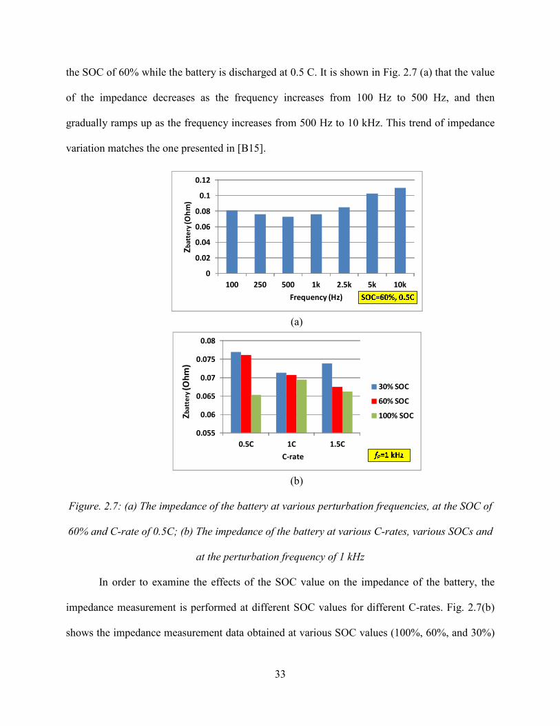
33
the SOC of 60% while the battery is discharged at 0.5 C. It is shown in Fig. 2.7 (a) that the value
of the impedance decreases as the frequency increases from 100 Hz to 500 Hz, and then
gradually ramps up as the frequency increases from 500 Hz to 10 kHz. This trend of impedance
variation matches the one presented in [B15].
0
0.02
0.04
0.06
0.08
0.1
0.12
100 250 500 1k 2.5k 5k 10k
Zb
att
ery
(O
hm
)
Frequency (Hz)
(a)
0.055
0.06
0.065
0.07
0.075
0.08
0.5C 1C 1.5C
Zb
att
ery
(O
hm
)
C-rate
30% SOC
60% SOC
100% SOC
(b)
Figure. 2.7: (a) The impedance of the battery at various perturbation frequencies, at the SOC of
60% and C-rate of 0.5C; (b) The impedance of the battery at various C-rates, various SOCs and
at the perturbation frequency of 1 kHz
In order to examine the effects of the SOC value on the impedance of the battery, the
impedance measurement is performed at different SOC values for different C-rates. Fig. 2.7(b)
shows the impedance measurement data obtained at various SOC values (100%, 60%, and 30%)
34
and various C-rates (0.5 C, 1 C, and 1.5 C) when the duty cycle of the power converter is
perturbed at 1 kHz. It can be observed from Fig. 2.7(b) that the impedance of the lithium-ion
battery increases with the depth of discharge (DOD) for different C-rates. For example, when the
battery is discharged at 0.5 C, the impedance of the battery increases from 65.28 mΩ to 76.92
mΩ as the SOC decreases from 100% to 30%. The experimental results/data at 1C and 1.5C
discharge rates show similar trends. Note that the measured impedance of the battery at 1 kHz
closely matches the one provided in the specification of the battery [B8].
Fig. 2.8 shows sample experimental waveforms during the process of the impedance
measurements using the proposed method under selected frequency values and combinations of
SOC and C-rate. Each waveform includes, from top to bottom, the voltage of the battery, the
current of the battery, and the output voltage of the power converter. From the experimental
waveforms shown in Fig. 2.8, it can clearly be observed that the sinusoidal ripple values of the
output voltage of the power converter caused by the duty cycle perturbation are less than 5% of
the corresponding DC values in most cases, and less than 10% of the corresponding DC values in
all cases. This indicates that the proposed method does not interrupt the normal operation of the
power converter. In addition, the complete impedance measurement process takes only a few
sinusoidal perturbation cycles (five in this paper). These two features make the proposed
impedance measurement method ideal for online applications. It should also be noted that the
sinusoidal ripple values could be reduced by using smaller duty cycle perturbation values.
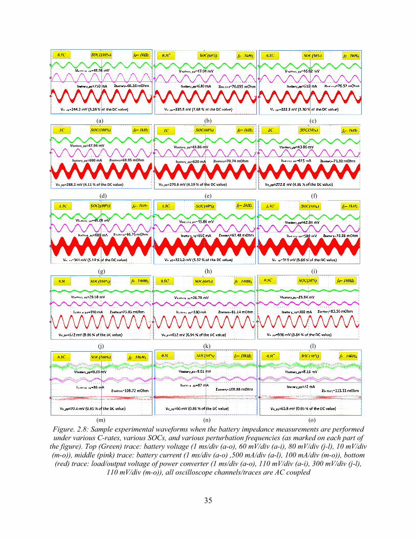
35
(a) (b) (c)
fp= 1kHz1C SOC(100%)
Vbattery_pp=47.94 mV
Vo_pp=288.2 mV (4.11 % of the DC value)
Ibattery_pp=690 mA zbattery=69.95 mOhm
fp= 1kHz1C SOC(60%)
Vbattery_pp=43.86 mV
Vo_pp=270.6 mV (4.19 % of the DC value)
Ibattery_pp=620 mA zbattery=70.74 mOhm
(d) (e) (f)
(g) (h) (i)
(j) (k) (l)
(m) (n) (o)
Figure. 2.8: Sample experimental waveforms when the battery impedance measurements are performed
under various C-rates, various SOCs, and various perturbation frequencies (as marked on each part of
the figure). Top (Green) trace: battery voltage (1 ms/div (a-o), 60 mV/div (a-i), 80 mV/div (j-l), 10 mV/div
(m-o)), middle (pink) trace: battery current (1 ms/div (a-o) ,500 mA/div (a-l), 100 mA/div (m-o)), bottom
(red) trace: load/output voltage of power converter (1 ms/div (a-o), 110 mV/div (a-i), 300 mV/div (j-l),
110 mV/div (m-o)), all oscilloscope channels/traces are AC coupled
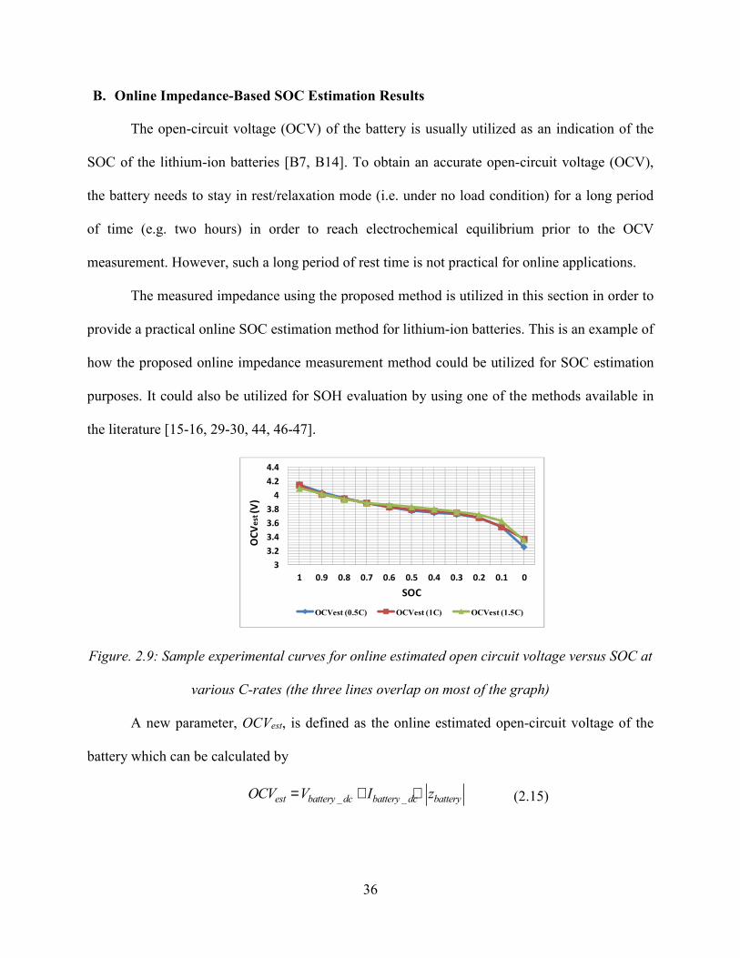
36
B. Online Impedance-Based SOC Estimation Results
The open-circuit voltage (OCV) of the battery is usually utilized as an indication of the
SOC of the lithium-ion batteries [B7, B14]. To obtain an accurate open-circuit voltage (OCV),
the battery needs to stay in rest/relaxation mode (i.e. under no load condition) for a long period
of time (e.g. two hours) in order to reach electrochemical equilibrium prior to the OCV
measurement. However, such a long period of rest time is not practical for online applications.
The measured impedance using the proposed method is utilized in this section in order to
provide a practical online SOC estimation method for lithium-ion batteries. This is an example of
how the proposed online impedance measurement method could be utilized for SOC estimation
purposes. It could also be utilized for SOH evaluation by using one of the methods available in
the literature [15-16, 29-30, 44, 46-47].
3
3.2
3.4
3.6
3.8
4
4.2
4.4
1 0.9 0.8 0.7 0.6 0.5 0.4 0.3 0.2 0.1 0
OC
Ve
st(V
)
SOC
OCVest (0.5C) OCVest (1C) OCVest (1.5C)
Figure. 2.9: Sample experimental curves for online estimated open circuit voltage versus SOC at
various C-rates (the three lines overlap on most of the graph)
A new parameter, OCVest, is defined as the online estimated open-circuit voltage of the
battery which can be calculated by
_ _est battery dc battery dc batteryOCV V I z= + ⋅ (2.15)
37
where |Zbattery| is the magnitude of the battery impedance in Ω, Vbattery_dc is the DC voltage of the
battery in volts with the direction shown in Fig. 2.3, and Ibattery_dc is the DC current of the battery
in amperes with the direction shown in Fig. 2.3. Ibattery_dc is positive when the battery is
discharging and is negative when the battery is charging.
Based on the information of the battery impedance at 1 kHz (as an example) which were
presented earlier in this section, and in combination with the measured DC voltage and DC
current of the battery, the OCVest versus SOC curves at various C-rates are plotted as shown in
Fig. 2.9. It can be observed from Fig. 2.9 that these curves almost overlap. Therefore, this curve
can be utilized to perform a simple online SOC estimation. Once the impedance of the battery is
obtained, OCVest can be calculated based on (2.15) and then the corresponding SOC value can be
estimated by mapping the calculated OCVest value to the OCVest versus SOC curve shown in Fig.
2.9.
C. Comments on Temperature Effect on The SOC Estimation for Lithium-Ion Batteries
Temperature is a key factor that affects the accuracy of the SOC estimation [15-17, 27,
48-49, 52, 57-58], which has not been sufficiently addressed in the literature. For example, in the
conventional coulomb counting method, the value of the battery capacity is usually assumed to
be the rated capacity at a nominal temperature without compensation as a function of the
temperature [16]. Other example SOC estimation methods include model-based methods [48-
49]. While in these model-based methods the Resistance-Capacitance (RC) parameters of the
battery model account for the temperature effects, other variables like OCV that are also
temperature dependent are not accounted for. In the proposed online impedance-based SOC
estimation method for lithium-ion batteries, in addition to taking the temperature effects into
account in the measured battery impedance itself, different OCVest versus SOC curves at
38
different operating temperatures can be measured if needed in order to further compensate for the
temperature variations. Based on the real-time measured temperature value of the battery, the
corresponding OCVest versus SOC curve can be used for SOC estimation.
2.4 Summary
This chapter first presents a basic online impedance measurement method for
electrochemical batteries. Instead of performing external AC voltage/current signal injection, the
impedance measurement is achieved through the control of the DC-DC power converter
interfacing the battery with the load/system. As a result, the signal generation circuits/devices
required by the conventional impedance measurement methods are eliminated, leading to
reduced cost, design complexities and size of the overall system.
The proposed online impedance measurement method can be performed either
continuously or periodically without interrupting the normal operation of the battery system and
power converter. Also, the complete impedance measurement process takes only a few
perturbation cycles, which makes the proposed method well suited for real-time battery
impedance monitoring.
In addition, a practical online SOC estimation method for lithium-ion batteries is
provided in this chapter based on the obtained information of the battery impedance. With the
proposed method, there is no need to put the battery in rest/relaxation mode for a long period of
time in order for the battery to reach electrochemical equilibrium prior to the OCV measurement.
Experimental results have validated the effectiveness of the proposed online impedance
measurement method and its utilization in the online SOC estimation.
39
CHAPTER 3
ENERGY SHARING CONTROLLER IN BATTERY DISCHARGE MODE
3.1 Introduction
This chapter presents an energy sharing based cell balancing control scheme for a
distributed battery energy storage system architecture where the cell balancing system and the
DC bus voltage regulation system are combined into a single system. The battery cells are
decoupled from one another by connecting each cell with a small lower power DC-DC power
converter. The small power converters are utilized to achieve both SOC balancing between the
battery cells and DC bus voltage regulation at the same time. The battery cells’ SOC imbalance
issue is addressed from the root by using the energy sharing concept to automatically adjust the
discharge/charge rate of each cell while maintaining a regulated DC bus voltage. Consequently,
there is no need to transfer the excess charge/energy between the cells for SOC balancing which
leads to reduced power losses.
In this chapter, the conventional centralized battery energy storage architecture is first
reviewed in Section II where the cell balancing issue and commonly used solutions are reviewed.
Section III presents the basic concept behind the distributed battery energy storage system
architecture which the proposed energy sharing controller will be used for. The operational
principle of the proposed energy sharing controller is discussed for discharging operation in
Section IV. Theoretical steady-state analysis of the proposed energy sharing SOC balancing
system during discharging operation is presented in Section V. Proof-of-concept experimental
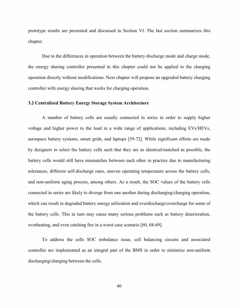
40
prototype results are presented and discussed in Section VI. The last section summarizes this
chapter.
Due to the differences in operation between the battery discharge mode and charge mode,
the energy sharing controller presented in this chapter could not be applied to the charging
operation directly without modifications. Next chapter will propose an upgraded battery charging
controller with energy sharing that works for charging operation.
3.2 Centralized Battery Energy Storage System Architecture
A number of battery cells are usually connected in series in order to supply higher
voltage and higher power to the load in a wide range of applications, including EVs/HEVs,
aerospace battery systems, smart grids, and laptops [59-72]. While significant efforts are made
by designers to select the battery cells such that they are as identical/matched as possible, the
battery cells would still have mismatches between each other in practice due to manufacturing
tolerances, different self-discharge rates, uneven operating temperature across the battery cells,
and non-uniform aging process, among others. As a result, the SOC values of the battery cells
connected in series are likely to diverge from one another during discharging/charging operation,
which can result in degraded battery energy utilization and overdischarge/overcharge for some of
the battery cells. This in turn may cause many serious problems such as battery deterioration,
overheating, and even catching fire in a worst case scenario [60, 68-69].
To address the cells SOC imbalance issue, cell balancing circuits and associated
controller are implemented as an integral part of the BMS in order to minimize non-uniform
discharging/charging between the cells.
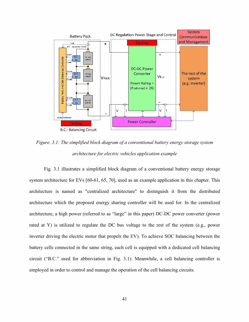
41
Figure. 3.1: The simplified block diagram of a conventional battery energy storage system
architecture for electric vehicles application example
Fig. 3.1 illustrates a simplified block diagram of a conventional battery energy storage
system architecture for EVs [60-61, 65, 70], used as an example application in this chapter. This
architecture is named as "centralized architecture" to distinguish it from the distributed
architecture which the proposed energy sharing controller will be used for. In the centralized
architecture, a high power (referred to as “large” in this paper) DC-DC power converter (power
rated at Y) is utilized to regulate the DC bus voltage to the rest of the system (e.g., power
inverter driving the electric motor that propels the EV). To achieve SOC balancing between the
battery cells connected in the same string, each cell is equipped with a dedicated cell balancing
circuit (“B.C.” used for abbreviation in Fig. 3.1). Meanwhile, a cell balancing controller is
employed in order to control and manage the operation of the cell balancing circuits.
42
A wide variety of cell balancing methods have been presented in the literature [59, 61-67,
73-79]. In general, the cell balancing methods fall under two main categories: passive and active
cell balancing schemes. Table 3.1 shows the classification of some example cell balancing
methods presented in the literature. A typical passive cell balancing method is to connect a shunt
resistor and a switch in parallel with each battery cell [59]. The excess energy is dissipated
through the shunt resistors in the form of heat. This scheme has the advantages of low cost,
simple circuit configuration, and ease of implementation. However, this comes at the expense of
additional energy dissipation and heat.
Table 3.1: Classification of Some Example Cell Balancing Methods
BALANCING
CATECORY
TECHNIQUE PROS CONS LITERATURE
Passive Shunt resistor Simple Low cost
0% efficiency [59]
Active Cell to cell (charge transfer between adjacent cells)
Relatively simple Modest control
complexity
Low efficiency Low balancing
speed
[61][62]
Active Cell to cell (charge transfer between arbitrary cells through multi-winding transformer)
High efficiency High balancing speed
Not practical if cell count is high
Hard to fabricate symmetrical windings
[63]
Active Cell to module (charge transfer between galvanic isolated converter)
Relatively simple Modest efficiency High balancing speed
High power isolated converter
Complicated control
[76][77]
Active Cell bypassing (cell disconnected from the current path)
Relatively simple Modest balancing
speed
High current switch
Low efficiency
[78][79]
Active cell balancing methods are more promising to be utilized in the next-generation
EVs/PHEVs and smart grid battery energy storage systems due to its ability to achieve high
efficiency. Instead of dissipating the excess energy, active cell balancing methods achieve cell
balancing by transferring the excess energy between the battery cells. Depending on how the
43
energy is redistributed between the cells, active cell balancing methods can be classified into the
following categories: cell to cell, cell to module, bypassing. In general, the efficiency of the
active balancing circuits with appropriate design is above 90% compared to 0% efficiency of
passive balancing.
Switched-capacitor based circuits are commonly used to transfer energy between cells,
thanks to its simplicity [61]. To achieve higher efficiency of energy transfer, resonant switched-
capacitor balancing circuit can be utilized such as the one presented in [62], where a small
inductor is added to form a resonant tank with the capacitor. Zero-current switching (ZCS)
operation can be achieved at the turn-off switching transition of the MOSFETs, leading to
reduced power losses. However, with this type of balancing circuit, energy are only transferred
between adjacent battery cells. If the energy is to be transferred from the battery cell on one end
of the battery string to the cell on the other end, a significant portion of the energy can be lost
along the energy transfer path.
To overcome this issue, multi-winding transformer based balancing circuits can be
utilized, as in [63]. The balancing circuit topology presented in [63] allows the energy to be
transferred between arbitrary cells in the battery string. However, the multi-winding transformer
based balancing circuits typically suffer from two major issues. The first issue is that the
balancing performance of the circuit depends heavily on the symmetry of the transformer
windings. Another issue is that it is difficult to fabricate a transformer with several tens or
hundreds of symmetrical windings for high power applications where a large number of battery
cells are connected in series. A common solution to this issue would be to modularize the battery
cells and then use an additional balancing circuit stage to balance the modules. However, this
would lead to increased system design complexity, cost and size.
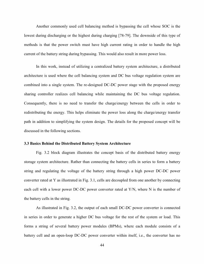
44
Another commonly used cell balancing method is bypassing the cell whose SOC is the
lowest during discharging or the highest during charging [78-79]. The downside of this type of
methods is that the power switch must have high current rating in order to handle the high
current of the battery string during bypassing. This would also result in more power loss.
In this work, instead of utilizing a centralized battery system architecture, a distributed
architecture is used where the cell balancing system and DC bus voltage regulation system are
combined into a single system. The re-designed DC-DC power stage with the proposed energy
sharing controller realizes cell balancing while maintaining the DC bus voltage regulation.
Consequently, there is no need to transfer the charge/energy between the cells in order to
redistributing the energy. This helps eliminate the power loss along the charge/energy transfer
path in addition to simplifying the system design. The details for the proposed concept will be
discussed in the following sections.
3.3 Basics Behind the Distributed Battery System Architecture
Fig. 3.2 block diagram illustrates the concept basis of the distributed battery energy
storage system architecture. Rather than connecting the battery cells in series to form a battery
string and regulating the voltage of the battery string through a high power DC-DC power
converter rated at Y as illustrated in Fig. 3.1, cells are decoupled from one another by connecting
each cell with a lower power DC-DC power converter rated at Y/N, where N is the number of
the battery cells in the string.
As illustrated in Fig. 3.2, the output of each small DC-DC power converter is connected
in series in order to generate a higher DC bus voltage for the rest of the system or load. This
forms a string of several battery power modules (BPMs), where each module consists of a
battery cell and an open-loop DC-DC power converter within itself, i.e., the converter has no
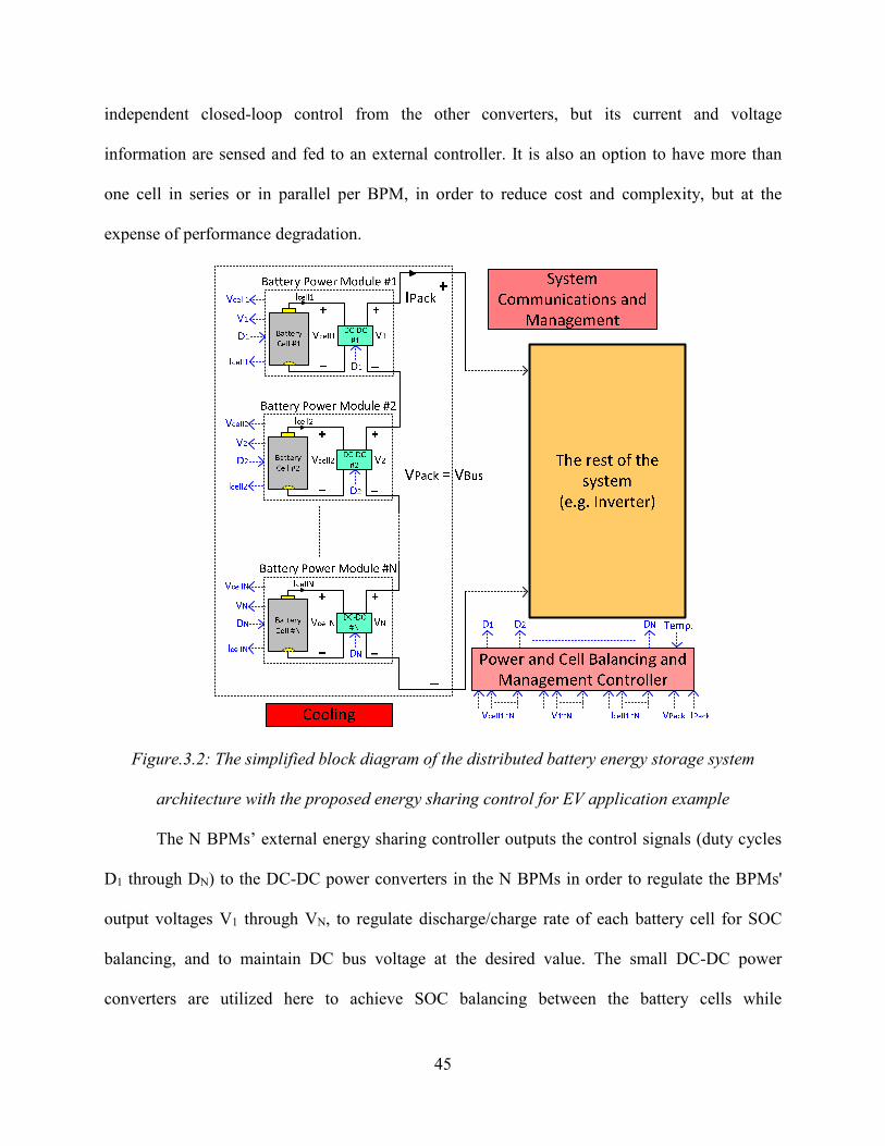
45
independent closed-loop control from the other converters, but its current and voltage
information are sensed and fed to an external controller. It is also an option to have more than
one cell in series or in parallel per BPM, in order to reduce cost and complexity, but at the
expense of performance degradation.
Figure.3.2: The simplified block diagram of the distributed battery energy storage system
architecture with the proposed energy sharing control for EV application example
The N BPMs’ external energy sharing controller outputs the control signals (duty cycles
D1 through DN) to the DC-DC power converters in the N BPMs in order to regulate the BPMs'
output voltages V1 through VN, to regulate discharge/charge rate of each battery cell for SOC
balancing, and to maintain DC bus voltage at the desired value. The small DC-DC power
converters are utilized here to achieve SOC balancing between the battery cells while
46
maintaining DC bus voltage regulation. Therefore, there is no need to use two independent
converter systems for cell balancing and DC bus voltage regulation as seen in the centralized
architecture. This leads to reduced system design complexity. Moreover, from the system point
of view, if the small low-power DC-DC converters are well designed with comparable or higher
efficiency than the big high-power DC-DC converter that is utilized in the conventional
architecture, the cell balancing is achieved with effectively 100% efficiency in the proposed
architecture (i.e., there are no additional power losses caused by cells SOC balancing operation).
The small DC-DC power converter used in each BPM needs to be bidirectional in order
to allow for both charging and discharging operations. The DC-DC power converter needs to be
of the isolated type when isolation is required. A variety of candidate isolated and non-isolated
topologies are available for this application [71-72, 80-83, 92-94]. For simplification, the
conventional non-isolated bidirectional DC-DC buck/boost converter is used in this work for
illustration and verification. This bidirectional power converter operates as a DC-DC boost
converter with the battery cell as the input and the DC bus as the output during discharging
operation, and operates as a DC-DC buck converter with the DC bus as the input and the battery
cell as the output during charging operation. The selection of the power converter circuit
topology is a function of many variables such as the target BPM power rating, power conversion
efficiency, power density, cost, integration/packaging simplicity, and EMI requirement.
It should be noted that the output-series connected multiple converters architecture itself
is not new and has been utilized in many applications, such as those on photovoltaic applications
[84-86]. Another concept is presented in [87] which utilizes distributed battery architecture.
However, the basic concept in [87] is based on calculating the duty cycle values and discharge
intervals required to achieve cell balancing and output voltage regulation by using theoretical
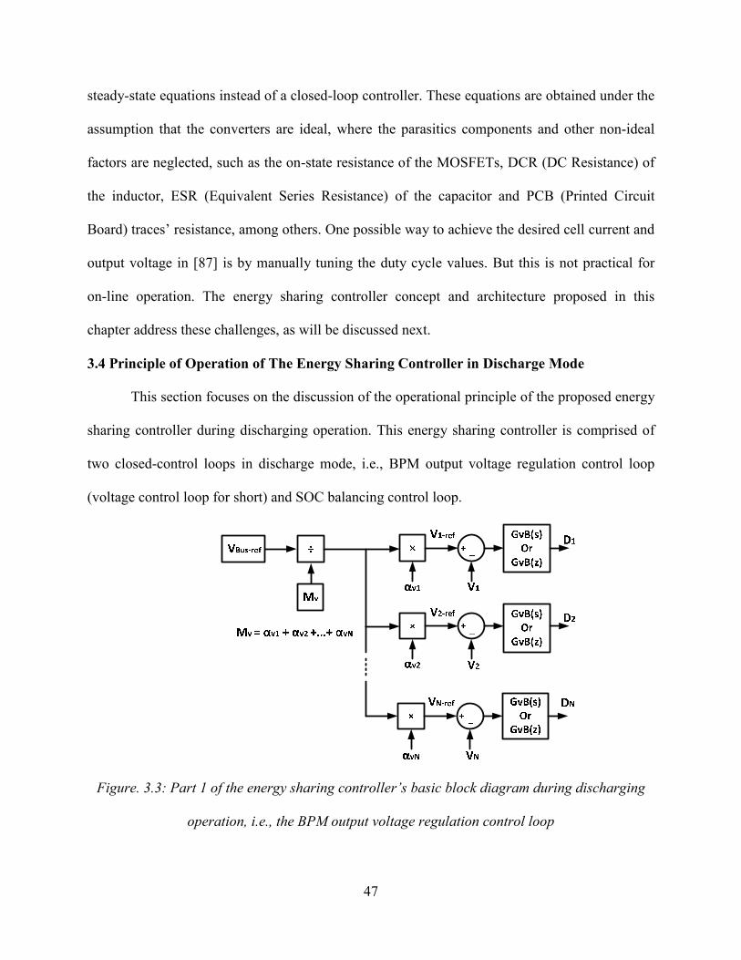
47
steady-state equations instead of a closed-loop controller. These equations are obtained under the
assumption that the converters are ideal, where the parasitics components and other non-ideal
factors are neglected, such as the on-state resistance of the MOSFETs, DCR (DC Resistance) of
the inductor, ESR (Equivalent Series Resistance) of the capacitor and PCB (Printed Circuit
Board) traces’ resistance, among others. One possible way to achieve the desired cell current and
output voltage in [87] is by manually tuning the duty cycle values. But this is not practical for
on-line operation. The energy sharing controller concept and architecture proposed in this
chapter address these challenges, as will be discussed next.
3.4 Principle of Operation of The Energy Sharing Controller in Discharge Mode
This section focuses on the discussion of the operational principle of the proposed energy
sharing controller during discharging operation. This energy sharing controller is comprised of
two closed-control loops in discharge mode, i.e., BPM output voltage regulation control loop
(voltage control loop for short) and SOC balancing control loop.
Figure. 3.3: Part 1 of the energy sharing controller’s basic block diagram during discharging
operation, i.e., the BPM output voltage regulation control loop
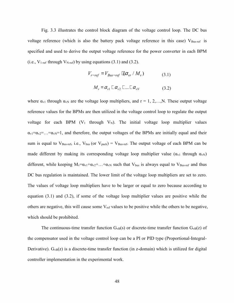
48
Fig. 3.3 illustrates the control block diagram of the voltage control loop. The DC bus
voltage reference (which is also the battery pack voltage reference in this case) VBus-ref is
specified and used to derive the output voltage reference for the power converter in each BPM
(i.e., V1-ref through VN-ref) by using equations (3.1) and (3.2).
( / )r ref Bus ref vr vV V Mα− −= ⋅ (3.1)
vNvvvM ααα +++= ...21 (3.2)
where αv1 through αvN are the voltage loop multipliers, and r = 1, 2,…,N. These output voltage
reference values for the BPMs are then utilized in the voltage control loop to regulate the output
voltage for each BPM (V1 through VN). The initial voltage loop multiplier values
αv1=αv2=…=αvN=1, and therefore, the output voltages of the BPMs are initially equal and their
sum is equal to VBus-ref, i.e., Vbus (or Vpack) = VBus-ref. The output voltage of each BPM can be
made different by making its corresponding voltage loop multiplier value (αv1 through αvN)
different, while keeping Mv=αv1+αv2+…+αvN such that Vbus is always equal to VBus-ref and thus
DC bus regulation is maintained. The lower limit of the voltage loop multipliers are set to zero.
The values of voltage loop multipliers have to be larger or equal to zero because according to
equation (3.1) and (3.2), if some of the voltage loop multiplier values are positive while the
others are negative, this will cause some Vref values to be positive while the others to be negative,
which should be prohibited.
The continuous-time transfer function GvB(s) or discrete-time transfer function GvB(z) of
the compensator used in the voltage control loop can be a PI or PID type (Proportional-Integral-
Derivative). GvB(z) is a discrete-time transfer function (in z-domain) which is utilized for digital
controller implementation in the experimental work.
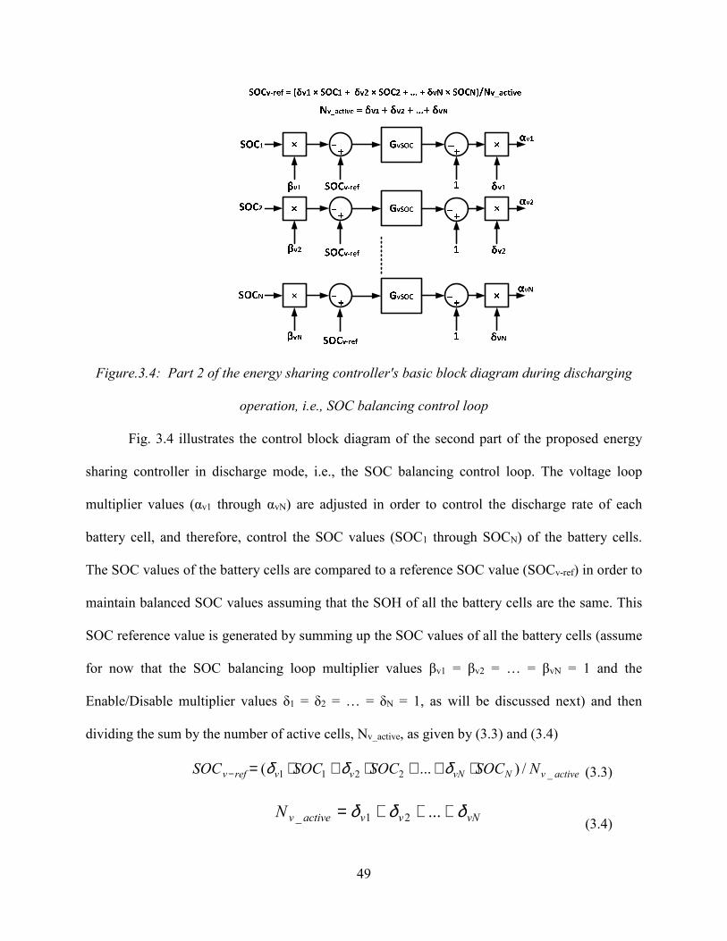
49
Figure.3.4: Part 2 of the energy sharing controller's basic block diagram during discharging
operation, i.e., SOC balancing control loop
Fig. 3.4 illustrates the control block diagram of the second part of the proposed energy
sharing controller in discharge mode, i.e., the SOC balancing control loop. The voltage loop
multiplier values (αv1 through αvN) are adjusted in order to control the discharge rate of each
battery cell, and therefore, control the SOC values (SOC1 through SOCN) of the battery cells.
The SOC values of the battery cells are compared to a reference SOC value (SOCv-ref) in order to
maintain balanced SOC values assuming that the SOH of all the battery cells are the same. This
SOC reference value is generated by summing up the SOC values of all the battery cells (assume
for now that the SOC balancing loop multiplier values βv1 = βv2 = … = βvN = 1 and the
Enable/Disable multiplier values δ1 = δ2 = … = δN = 1, as will be discussed next) and then
dividing the sum by the number of active cells, Nv_active, as given by (3.3) and (3.4)
activevNvNvvrefv NSOCSOCSOCSOC _2211 /)...( ⋅++⋅+⋅=− δδδ (3.3)
vNvvactivevN δδδ +++= ...21_
(3.4)
50
If the SOC value of a battery cell is smaller or larger than the SOC reference value (i.e.,
the other battery cells’ SOC values), this will affect its corresponding voltage loop multiplier
value which in turn affects the output voltage reference value for that specific BPM. Since the
output current of all BPMs in the string is the same, this different output voltage will affect the
discharge rate of that specific cell because the output power of a BPM in this case is a function
of the output voltage of the BPM. This operation will continue until the SOC values of all the
battery cells are balanced. Adjusting the output voltage of a BPM while maintaining the total DC
bus voltage regulated means that the energy drawn from that battery cell is controlled, which
controls the discharge rate of that battery cell. This energy sharing control concept automatically
and quickly results in SOC balancing between the battery cells in the battery pack. In Fig. 3.4,
the compensator’s transfer function GvSOC utilized in the SOC balancing control loop can also be
a PI or a PID type.
The plant that is controlled here is the control-to-output transfer function of the BPM
boost converter. The inner loop (voltage control loop) should be designed to be faster than the
outer SOC balancing control loop. The compensators, GvB and GvSOC, could be designed based
on the rule-of-thumb frequency-domain controller design guidelines and criteria which includes
crossover frequency (unit-gain bandwidth), stability margins. The detailed small-signal modeling
and energy sharing controller design are presented in Chapter 5.
The SOC balancing loop multipliers (βv1 through βvN) can be used to control (alter) the
desired SOC value for a specific battery cell in order to make the SOC or discharge rate of a
battery cell larger or smaller than it is for the rest of the battery cells. Each SOC balancing loop
multiplier can have positive values from 0 to 1. It can be a function of the SOH of the battery cell
(assuming that SOH information is available for each cell [68-69]). If this multiplier value is
51
larger, the SOC balancing control loop will think that this battery cell has a larger SOC value
than it actually has and therefore it will discharge the battery cell at a faster rate, and vice versa.
The βv1 through βvN multipliers are added to the proposed controller for future utilization. These
multipliers are not utilized in this paper and their values are set to βv1 = βv2 = … = βvN = 1.
The Enable/Disable multipliers (δ1 through δN) have values of either 1 or 0 in order to
enable or disable a BPM control (if a BPM is to be removed from the system). Each BPM has
two output terminals which can be connected after removing/disconnecting a BPM in order to
maintain a working system. A BPM can manually be removed and the corresponding two
terminals in the corresponding socket can manually be shorted/connected. A possible future
work is to investigate methods to automatically realize bypassing of a BPM during online
operation. This might require adding extra components. The Enable/Disable multiplier δr for a
given BPM is set to zero only when the corresponding BPM is removed. When a BPM is
removed from the system, the corresponding voltage loop multiplier (αvr) for that BPM is equal
to 0 because δr = 0, as illustrated in Fig. 3.4, and the corresponding two output voltage terminals
for that BPM are shorted in order to provide current flowing path. Once an Enable/Disable
multiplier is set to zero, this will affect equations (3.2)-(3.4) and the SOC balancing and DC bus
voltage regulation operations will continue as they should assuming that the maximum allowed
output voltage of each BPM is not exceeded.
3.5 Steady-State Analysis of The Energy Sharing Controller in Discharge Mode
This section presents theoretical steady-state analysis of the energy sharing controlled
distributed battery system during discharging operation. Fig. 3.5 shows the system configuration.
To simplify analysis, assume that all the power converter components are ideal, which means the
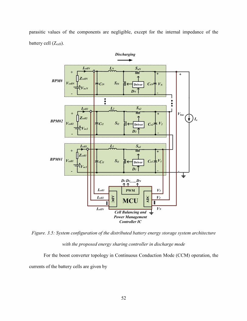
52
parasitic values of the components are negligible, except for the internal impedance of the
battery cell (Zcell).
SuN
SlN
LN
Driver
+
-DN
IcellN
+
-
Su2
Sl2
L2
Driver
+
-D2
Icell2
+
-
Su1
Sl1
L1
Driver
+
-
Vcell1
D1
Icell1
+
-
MCU
PWM
D1 D2 DN…..
VN
V2
V1
Vcell2
VcellN
VocN
Voc2
Voc1
Io
ZcellN
Zcell2
Zcell1
Icell1
Icell2
IcellN
V1
V2
VN
CoN
Co2
Ci1
BPM#
Cell Balancing and
Power Management
Controller IC
+
-
Vbus
BPM#2
BPM#1
CiN
Ci2
Co1
Discharging
Figure. 3.5: System configuration of the distributed battery energy storage system architecture
with the proposed energy sharing controller in discharge mode
For the boost converter topology in Continuous Conduction Mode (CCM) operation, the
currents of the battery cells are given by
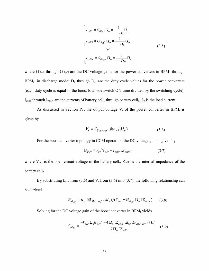
53
1 11
2 22
1
1
1
1
1
1
cell dhg o o
cell dhg o o
cellN dhgN o oN
I G I ID
I G I ID
I G I ID
= ⋅ = ⋅ − = ⋅ = ⋅ − = ⋅ = ⋅ −
M (3.5)
where Gdhg1 through GdhgN are the DC voltage gains for the power converters in BPM1 through
BPMN in discharge mode; D1 through DN are the duty cycle values for the power converters
(each duty cycle is equal to the boost low-side switch ON time divided by the switching cycle);
Icell1 through IcellN are the currents of battery cell1 through battery cellN. Io is the load current.
As discussed in Section IV, the output voltage Vr of the power converter in BPMr is
given by
( )r Bus ref vr vV V Mα−= ⋅ (3.6)
For the boost converter topology in CCM operation, the DC voltage gain is given by
( )dhgr r ocr cellr cellrG V V I Z= − ⋅ (3.7)
where Vocr is the open-circuit voltage of the battery cellr; Zcellr is the internal impedance of the
battery cellr.
By substituting Icellr from (3.5) and Vr from (3.6) into (3.7), the following relationship can
be derived
( ) ( )dhgr vr Bus ref v ocr dhgr o cellrG V M V G I Zα −= ⋅ − ⋅ ⋅ (3.8)
Solving for the DC voltage gain of the boost converter in BPMr yields
2 4 ( )
2
ocr ocr o cellr vr Bus ref v
dhgro cellr
V V I Z V MG
I Z
α −− ± − ⋅ ⋅ ⋅ ⋅=
− ⋅ ⋅ (3.9)
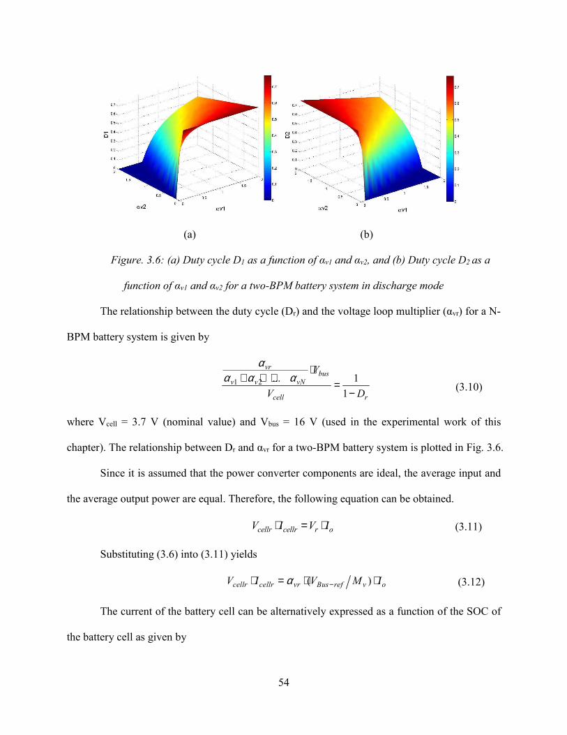
54
(a) (b)
Figure. 3.6: (a) Duty cycle D1 as a function of αv1 and αv2, and (b) Duty cycle D2 as a
function of αv1 and αv2 for a two-BPM battery system in discharge mode
The relationship between the duty cycle (Dr) and the voltage loop multiplier (αvr) for a N-
BPM battery system is given by
1 2 ... 1
1
vrbus
v v vN
cell r
V
V D
αα α α
⋅+ + + =
− (3.10)
where Vcell = 3.7 V (nominal value) and Vbus = 16 V (used in the experimental work of this
chapter). The relationship between Dr and αvr for a two-BPM battery system is plotted in Fig. 3.6.
Since it is assumed that the power converter components are ideal, the average input and
the average output power are equal. Therefore, the following equation can be obtained.
cellr cellr r oV I V I⋅ = ⋅ (3.11)
Substituting (3.6) into (3.11) yields
( )cellr cellr vr Bus ref v oV I V M Iα −⋅ = ⋅ ⋅ (3.12)
The current of the battery cell can be alternatively expressed as a function of the SOC of
the battery cell as given by
55
( )cellr rI Q dSOC dt= ⋅ (3.13)
where Q is the rated capacity of the battery cell, assuming that all the battery cells have the same
capacity.
By substituting (13) into (12), the following equation can be derived,
( ) ( )r vr Bus ref v o cellrdSOC dt V M I Q Vα −= ⋅ ⋅ ⋅ (3.14)
The proposed energy sharing controller dynamically control the voltage multiplier values
αv1 through αvN in order to achieve SOC balancing between the battery cells during discharging
operation.
3.6 Proof-Of-Concept Experimental Prototype Results
A. Experimental Setup
To validate and evaluate the performance of the proposed energy sharing controller, a
scaled-down distributed battery energy storage system prototype with the proposed energy
sharing controller is built in the laboratory. The system configuration of the experimental
prototype is illustrated in Fig. 3.5. The experimental prototype consists of two 18650-size
cylindrical lithium-ion battery cells, two bidirectional DC-DC synchronous buck/boost power
converters and a programmable DC electronic load (Chroma 6312) which is used to emulate the
rest of the system after the DC bus. The proposed energy sharing controller is implemented using
TMS320F28335 floating-point Microcontroller/DSP from Texas Instrument Inc. (TI). The digital
compensators used in the SOC balancing control loop and the voltage control loop are both of PI
type. The TMS320F28335 is simply utilized for the proof-of-concept prototyping, which has
more than needed processing power and capabilities for the two-cell prototype in this work. In an
actual product, depending on the number of cells and the desired performance, a controller with
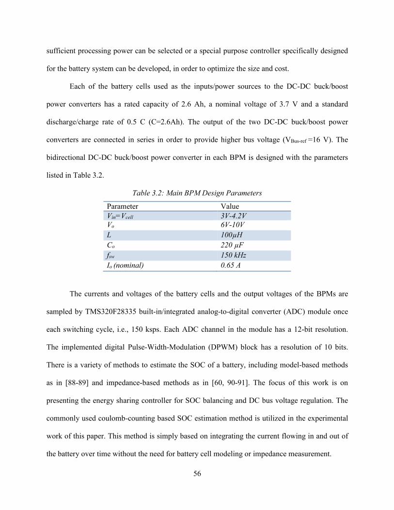
56
sufficient processing power can be selected or a special purpose controller specifically designed
for the battery system can be developed, in order to optimize the size and cost.
Each of the battery cells used as the inputs/power sources to the DC-DC buck/boost
power converters has a rated capacity of 2.6 Ah, a nominal voltage of 3.7 V and a standard
discharge/charge rate of 0.5 C (C=2.6Ah). The output of the two DC-DC buck/boost power
converters are connected in series in order to provide higher bus voltage (VBus-ref =16 V). The
bidirectional DC-DC buck/boost power converter in each BPM is designed with the parameters
listed in Table 3.2.
Table 3.2: Main BPM Design Parameters
Parameter Value
Vin=Vcell 3V-4.2V
Vo 6V-10V
L 100µH
Co 220 µF
fsw 150 kHz
Io (nominal) 0.65 A
The currents and voltages of the battery cells and the output voltages of the BPMs are
sampled by TMS320F28335 built-in/integrated analog-to-digital converter (ADC) module once
each switching cycle, i.e., 150 ksps. Each ADC channel in the module has a 12-bit resolution.
The implemented digital Pulse-Width-Modulation (DPWM) block has a resolution of 10 bits.
There is a variety of methods to estimate the SOC of a battery, including model-based methods
as in [88-89] and impedance-based methods as in [60, 90-91]. The focus of this work is on
presenting the energy sharing controller for SOC balancing and DC bus voltage regulation. The
commonly used coulomb-counting based SOC estimation method is utilized in the experimental
work of this paper. This method is simply based on integrating the current flowing in and out of
the battery over time without the need for battery cell modeling or impedance measurement.
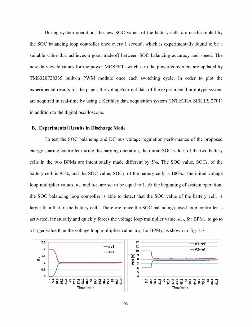
57
During system operation, the new SOC values of the battery cells are used/sampled by
the SOC balancing loop controller once every 1 second, which is experimentally found to be a
suitable value that achieves a good tradeoff between SOC balancing accuracy and speed. The
new duty cycle values for the power MOSFET switches in the power converters are updated by
TMS320F28335 built-in PWM module once each switching cycle. In order to plot the
experimental results for the paper, the voltage/current data of the experimental prototype system
are acquired in real-time by using a Keithley data acquisition system (INTEGRA SERIES 2701)
in addition to the digital oscilloscope.
B. Experimental Results in Discharge Mode
To test the SOC balancing and DC bus voltage regulation performance of the proposed
energy sharing controller during discharging operation, the initial SOC values of the two battery
cells in the two BPMs are intentionally made different by 5%. The SOC value, SOC1, of the
battery cell1 is 95%, and the SOC value, SOC2, of the battery cell2 is 100%. The initial voltage
loop multiplier values, αv1 and αv2, are set to be equal to 1. At the beginning of system operation,
the SOC balancing loop controller is able to detect that the SOC value of the battery cell2 is
larger than that of the battery cell1. Therefore, once the SOC balancing closed loop controller is
activated, it naturally and quickly forces the voltage loop multiplier value, αv2, for BPM2 to go to
a larger value than the voltage loop multiplier value, αv1, for BPM1, as shown in Fig. 3.7.
0
0.5
1
1.5
2
2.5
0
5.4
10
.8
16
.2
21
.6 27
32
.4
37
.8
43
.2
48
.6 54
59
.4
64
.8
70
.2
75
.6 81
86
.4
91
.8
av
Time (min)
av1
av2
4
5
6
7
8
9
10
11
12
0
5.4
10
.8
16
.2
21
.6 27
32
.4
37
.8
43
.2
48
.6 54
59
.4
64
.8
70
.2
75
.6 81
86
.4
91
.8
Vre
f (V
)
Time(min)
V1-ref
V2-ref
58
(a) (b)
00.10.20.30.40.50.60.70.80.9
11.1
0
5.4
10
.8
16
.2
21
.6 27
32
.4
37
.8
43
.2
48
.6 54
59
.4
64
.8
70
.2
75
.6 81
86
.4
91
.8
SO
C
Time (min)
SOC1
SOC2
(c) (d)
Figure. 3.7: Experimental results for (a) voltage multiplier values; (b) BPM output voltage
reference values; (c) from top to bottom: bus voltage, the output voltage for BPM2, the output
voltage for BPM1, the current of the battery cell2, and the current of the battery cell1; (d) SOC
values of the two battery cells, as the proposed energy sharing controller achieves SOC
balancing during battery discharging operation under 5% initial SOC difference between the
two battery cells
It can be observed from Fig. 3.7 (a) that αv2 reaches the pre-set maximum saturation
value, αvmax = 2, while αv1 reaches the pre-set minimum saturation value, αvmin = 0. This is in
order to make the output voltage of BPM2 larger than the output voltage of BPM1 in order to
discharge battery cell2 faster until SOC balancing is achieved. It can also be observed from Fig.
3.7 (a) that the voltage multiplier values get closer to each other by time until they are both
approximately equal to one when both battery cells have the same SOC values as they discharge.
Note that the reason why the voltage loop multiplier values are not exactly equal to one after the
SOC values get balanced is that the power converters in the two BPMs are not exactly
symmetrical due to components manufacturing tolerance, non-uniform PCB traces parasitics and
59
wiring/connections, among others. The SOC balancing control loop will automatically adjust the
voltage loop multiplier values such that the desired SOC balancing is achieved and maintained.
As discussed in Section IV, the BPM output voltage reference for the BPMr is equal to Vr-
ref = VBus-ref *(αvr/Mv). Based on this, once the energy sharing controller is activated, the output
voltage reference for BPM2, V2-ref, should be equal to VBus-ref=16 V while the output voltage
reference for BPM1, V1-ref, should be equal to 0 V. However, because the power converter
operates as a boost converter in the discharge mode, the output voltage of the BPM should be
higher than the input voltage (i.e., cell voltage, 3 V-4.2 V). For this reason, the minimum output
voltage reference value, Vmin-ref, is set to 6 V in this case, while the maximum output voltage
reference, Vmax-ref, is set to 10 V (Vmax-ref +Vmin-ref =VBus-ref =16 V). Therefore, V1-ref is forced to
be 6 V at the beginning of the operation, while V2-ref is forced to be 10 V, as shown in the
experimental result of Fig. 3.7 (b). Then, these two output voltage reference values are utilized in
the voltage control loop to regulate the output voltages (V1 and V2) for the two BPMs, as shown
in Fig. 3.7 (c). The output power for each BPM is a function of the output voltage for the BPM
under the same output current. Therefore, the battery cell2 is discharged at a faster rate than the
battery cell1 at the beginning of the operation, as shown in Fig. 3.7 (d), where the SOC values of
the two battery cells are plotted based on the acquired experimental data. It can also be observed
from Fig. 3.7 (c) and (d) that as the controller operation progresses, the SOC values of the two
battery cells gradually converge closer to each other which in turn makes the output voltage
differences between the two BPMs to decrease gradually. Therefore, the discharge rates of the
two battery cells gradually get closer to each other. As a result of the proper operation of the
energy sharing controller, the SOC values of the two battery cells get balanced approximately
t=10.8 minutes after the system operation starts, as shown in Fig. 3.7 (d). After that, the output
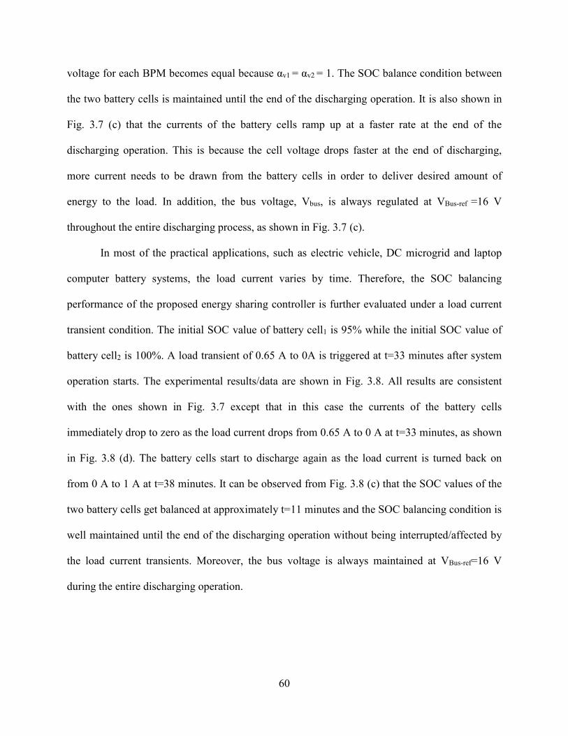
60
voltage for each BPM becomes equal because αv1 = αv2 = 1. The SOC balance condition between
the two battery cells is maintained until the end of the discharging operation. It is also shown in
Fig. 3.7 (c) that the currents of the battery cells ramp up at a faster rate at the end of the
discharging operation. This is because the cell voltage drops faster at the end of discharging,
more current needs to be drawn from the battery cells in order to deliver desired amount of
energy to the load. In addition, the bus voltage, Vbus, is always regulated at VBus-ref =16 V
throughout the entire discharging process, as shown in Fig. 3.7 (c).
In most of the practical applications, such as electric vehicle, DC microgrid and laptop
computer battery systems, the load current varies by time. Therefore, the SOC balancing
performance of the proposed energy sharing controller is further evaluated under a load current
transient condition. The initial SOC value of battery cell1 is 95% while the initial SOC value of
battery cell2 is 100%. A load transient of 0.65 A to 0A is triggered at t=33 minutes after system
operation starts. The experimental results/data are shown in Fig. 3.8. All results are consistent
with the ones shown in Fig. 3.7 except that in this case the currents of the battery cells
immediately drop to zero as the load current drops from 0.65 A to 0 A at t=33 minutes, as shown
in Fig. 3.8 (d). The battery cells start to discharge again as the load current is turned back on
from 0 A to 1 A at t=38 minutes. It can be observed from Fig. 3.8 (c) that the SOC values of the
two battery cells get balanced at approximately t=11 minutes and the SOC balancing condition is
well maintained until the end of the discharging operation without being interrupted/affected by
the load current transients. Moreover, the bus voltage is always maintained at VBus-ref=16 V
during the entire discharging operation.
61
0
0.5
1
1.5
2
2.5
0
3.9
7.8
11
.7
15
.6
19
.5
23
.4
27
.3
31
.2
35
.1 39
42
.9
46
.8
50
.7
54
.6
58
.5
62
.4
66
.3
70
.2
av
Time (min)
av1
av2
4
5
6
7
8
9
10
11
12
0
3.9
7.8
11
.7
15
.6
19
.5
23
.4
27
.3
31
.2
35
.1 39
42
.9
46
.8
50
.7
54
.6
58
.5
62
.4
66
.3
70
.2
Vre
f
Time (min)
V1-ref
V2-ref
(a) (b)
00.10.20.30.40.50.60.70.80.9
11.1
0
3.9
7.8
11
.7
15
.6
19
.5
23
.4
27
.3
31
.2
35
.1 39
42
.9
46
.8
50
.7
54
.6
58
.5
62
.4
66
.3
70
.2
SO
C
Time (min)
SOC1
SOC2
(c) (d)
Figure. 3.8: Experimental results for (a) voltage multiplier values; (b) BPM output voltage
reference values; (c) SOC values of the two battery cells; (d) from top to bottom: bus voltage, the
output voltage for BPM2, the output voltage for BPM1, the current of the battery cell2, and the
current of the battery cell1, as the energy sharing controller achieves SOC balancing during
discharging under 5% initial SOC difference between the two battery cells and load current
transient
3.7 Summary
An energy sharing controller is proposed in this chapter based on a distributed battery
energy storage system architecture. The re-designed DC-DC power stage and the proposed
energy sharing controller are utilized to achieve SOC balancing between the battery cells while
providing DC bus voltage regulation to the rest of the system or load. As a result, there is no
need for two independent converter systems for cell SOC balancing and DC bus voltage
62
regulation. This leads to reduced design complexity of the battery energy storage system. The
proposed energy sharing controller addresses the battery cells' SOC imbalance issue from the
root by adjusting the discharge rate of each battery cell while maintaining total regulated DC bus
voltage. The energy transfer between the battery cells that is usually required in the conventional
cell balancing schemes is no longer needed, thus eliminating the power losses caused by the
charge/energy transfer process.
The experimental prototype results validate the performance of the proposed energy
sharing controller during discharging operation. The developed architecture and energy sharing
controller is candidate for many battery energy storage applications including EVs/PHEVs
(which utilize power distribution scheme that has a DC-DC power converter), DC microgrids,
aerospace battery systems, laptop computers battery packs, and other portable devices with
multi-cell battery energy storage.
63
CHAPTER 4
BATTERY CHARGING CONTROLLER WITH ENERGY SHARING
4.1 Introduction
The energy sharing controller proposed in last chapter addresses the cell balancing issue
during battery discharging operation with high cell balancing speed and efficiency while
eliminating the need for dedicated cell balancing circuits. Given the differences in the operation
nature between battery discharge and charge mode, the energy sharing controller proposed in the
last chapter is upgraded in this chapter in order to achieve cell balancing while the battery cells
are being charged.
In this chapter, a conventional battery charging control algorithm is first reviewed and
then integrated with the energy sharing control concept to produce a complete cell balancing
solution for charging mode. The principle of operation of the upgraded battery charging
controller with energy sharing is introduced and discussed. The steady-state analysis of the
energy sharing controlled distributed battery system is also presented in the context of charging
operation. Proof-of-concept experimental results are given to verify the feasibility of the
proposed concept. At the end of this chapter, several comments are provided in terms of the cost,
efficiency and complexity of the energy sharing controller for both discharging and charging
operation.
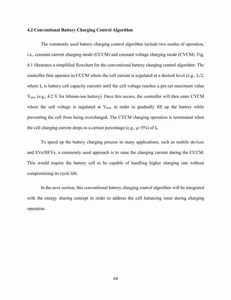
64
4.2 Conventional Battery Charging Control Algorithm
The commonly used battery charging control algorithm include two modes of operation,
i.e., constant current charging mode (CCCM) and constant voltage charging mode (CVCM). Fig.
4.1 illustrates a simplified flowchart for the conventional battery charging control algorithm. The
controller first operates in CCCM where the cell current is regulated at a desired level (e.g., Ic/2,
where Ic is battery cell capacity current) until the cell voltage reaches a pre-set maximum value
Vmax (e.g., 4.2 V for lithium-ion battery). Once this occurs, the controller will then enter CVCM
where the cell voltage is regulated at Vmax in order to gradually fill up the battery while
preventing the cell from being overcharged. The CVCM charging operation is terminated when
the cell charging current drops to a certain percentage (e.g., µ=5%) of Ic.
To speed up the battery charging process in many applications, such as mobile devices
and EVs/HEVs, a commonly used approach is to raise the charging current during the CCCM.
This would require the battery cell to be capable of handling higher charging rate without
compromising its cycle life.
In the next section, this conventional battery charging control algorithm will be integrated
with the energy sharing concept in order to address the cell balancing issue during charging
operation.
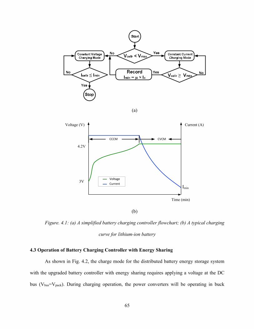
65
(a)
Voltage (V)
Time (min)
4.2V
3VVoltage
Current
Current (A)
Imin
CCCM CVCM
(b)
Figure. 4.1: (a) A simplified battery charging controller flowchart; (b) A typical charging
curve for lithium-ion battery
4.3 Operation of Battery Charging Controller with Energy Sharing
As shown in Fig. 4.2, the charge mode for the distributed battery energy storage system
with the upgraded battery controller with energy sharing requires applying a voltage at the DC
bus (Vbus=Vpack). During charging operation, the power converters will be operating in buck
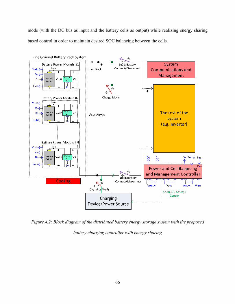
66
mode (with the DC bus as input and the battery cells as output) while realizing energy sharing
based control in order to maintain desired SOC balancing between the cells.
Figure.4.2: Block diagram of the distributed battery energy storage system with the proposed
battery charging controller with energy sharing
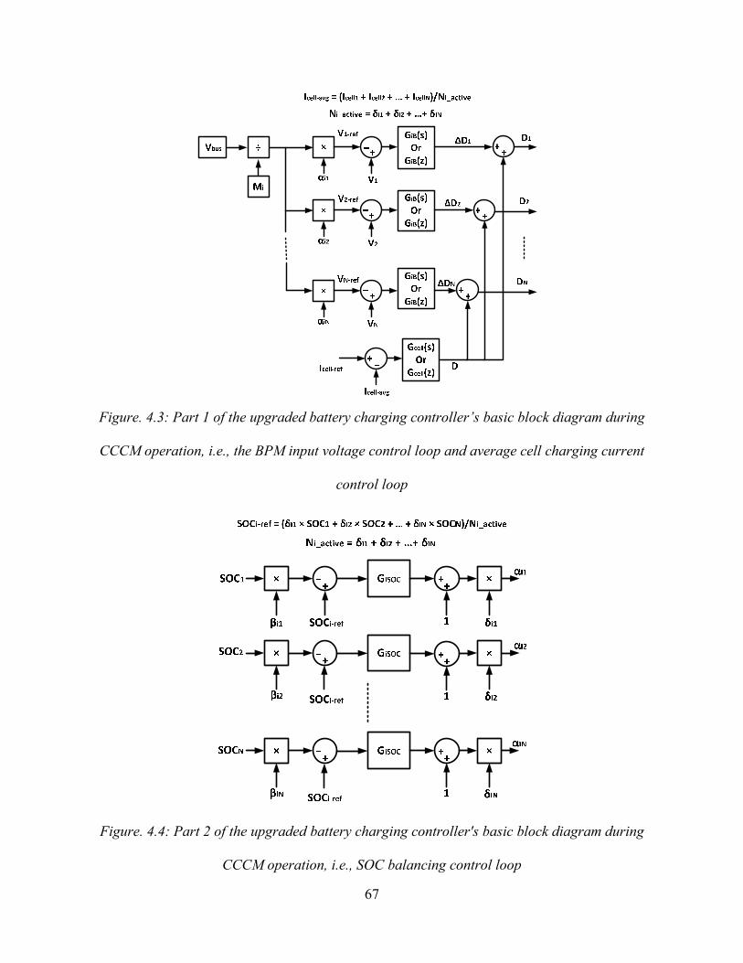
67
Figure. 4.3: Part 1 of the upgraded battery charging controller’s basic block diagram during
CCCM operation, i.e., the BPM input voltage control loop and average cell charging current
control loop
Figure. 4.4: Part 2 of the upgraded battery charging controller's basic block diagram during
CCCM operation, i.e., SOC balancing control loop
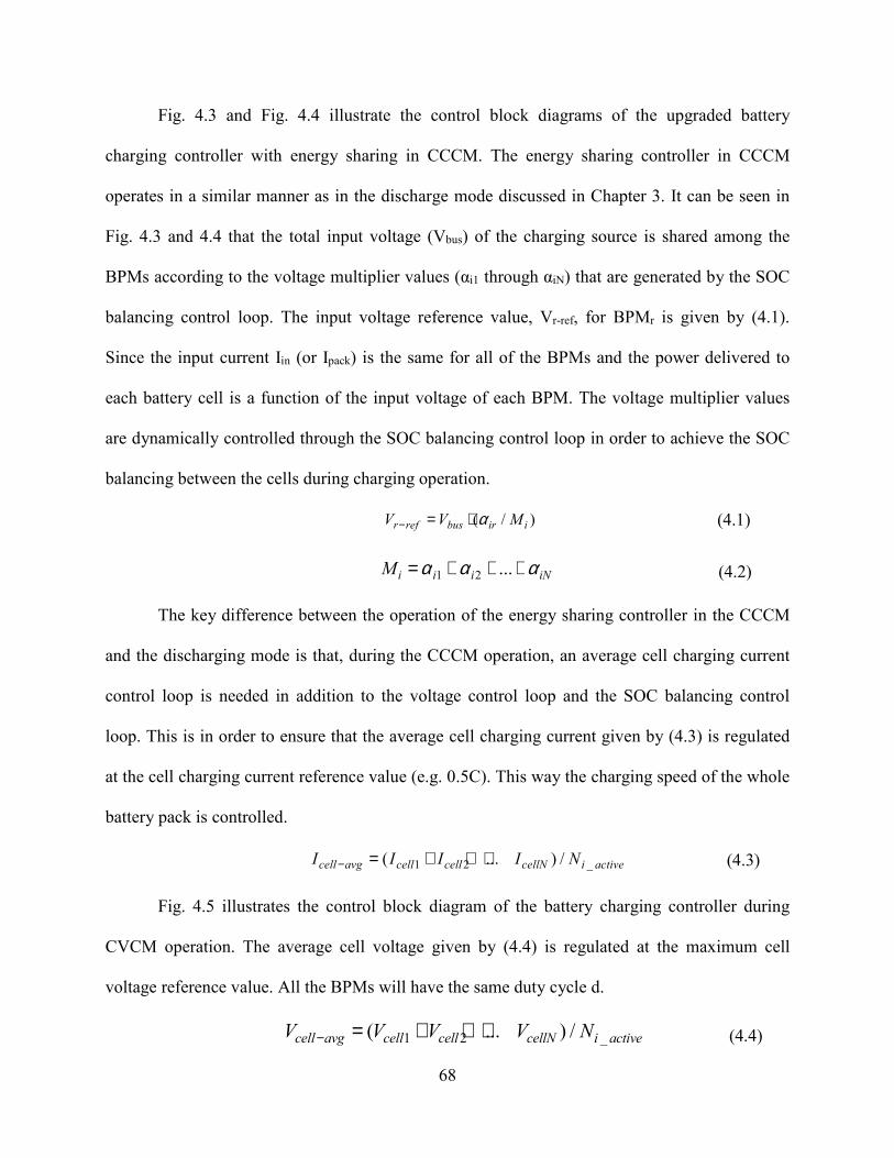
68
Fig. 4.3 and Fig. 4.4 illustrate the control block diagrams of the upgraded battery
charging controller with energy sharing in CCCM. The energy sharing controller in CCCM
operates in a similar manner as in the discharge mode discussed in Chapter 3. It can be seen in
Fig. 4.3 and 4.4 that the total input voltage (Vbus) of the charging source is shared among the
BPMs according to the voltage multiplier values (αi1 through αiN) that are generated by the SOC
balancing control loop. The input voltage reference value, Vr-ref, for BPMr is given by (4.1).
Since the input current Iin (or Ipack) is the same for all of the BPMs and the power delivered to
each battery cell is a function of the input voltage of each BPM. The voltage multiplier values
are dynamically controlled through the SOC balancing control loop in order to achieve the SOC
balancing between the cells during charging operation.
( / )r ref bus ir iV V Mα− = ⋅ (4.1)
iNiiiM ααα +++= ...21 (4.2)
The key difference between the operation of the energy sharing controller in the CCCM
and the discharging mode is that, during the CCCM operation, an average cell charging current
control loop is needed in addition to the voltage control loop and the SOC balancing control
loop. This is in order to ensure that the average cell charging current given by (4.3) is regulated
at the cell charging current reference value (e.g. 0.5C). This way the charging speed of the whole
battery pack is controlled.
1 2 _( ... ) /cell avg cell cell cellN i activeI I I I N− = + + + (4.3)
Fig. 4.5 illustrates the control block diagram of the battery charging controller during
CVCM operation. The average cell voltage given by (4.4) is regulated at the maximum cell
voltage reference value. All the BPMs will have the same duty cycle d.
1 2 _( ... ) /cell avg cell cell cellN i activeV V V V N− = + + + (4.4)
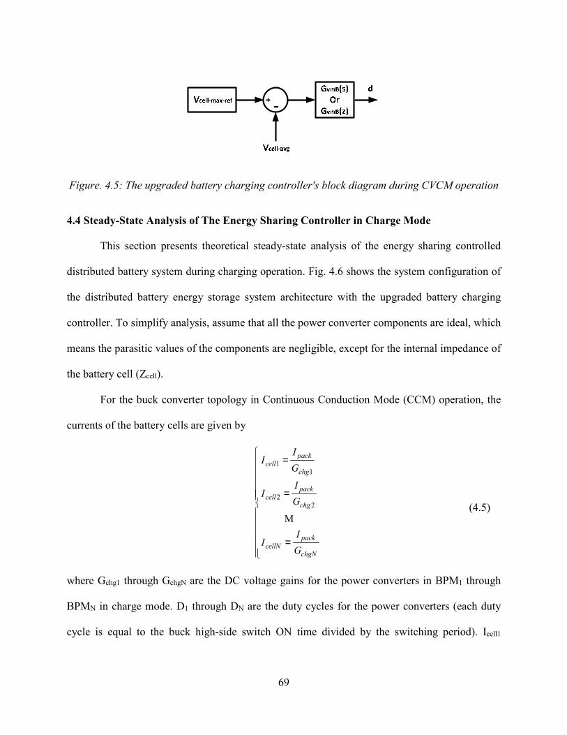
69
Figure. 4.5: The upgraded battery charging controller's block diagram during CVCM operation
4.4 Steady-State Analysis of The Energy Sharing Controller in Charge Mode
This section presents theoretical steady-state analysis of the energy sharing controlled
distributed battery system during charging operation. Fig. 4.6 shows the system configuration of
the distributed battery energy storage system architecture with the upgraded battery charging
controller. To simplify analysis, assume that all the power converter components are ideal, which
means the parasitic values of the components are negligible, except for the internal impedance of
the battery cell (Zcell).
For the buck converter topology in Continuous Conduction Mode (CCM) operation, the
currents of the battery cells are given by
11
22
packcell
chg
packcell
chg
packcellN
chgN
II
G
II
G
II
G
=
=
=
M (4.5)
where Gchg1 through GchgN are the DC voltage gains for the power converters in BPM1 through
BPMN in charge mode. D1 through DN are the duty cycles for the power converters (each duty
cycle is equal to the buck high-side switch ON time divided by the switching period). Icell1
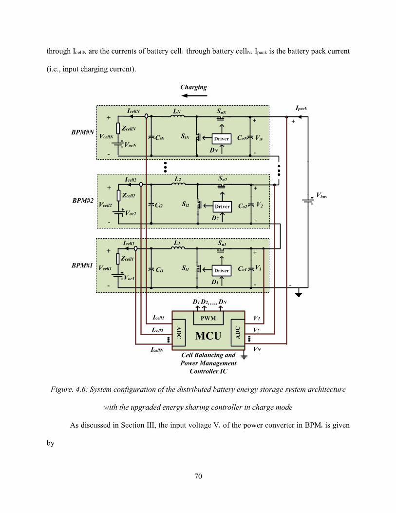
70
through IcellN are the currents of battery cell1 through battery cellN. Ipack is the battery pack current
(i.e., input charging current).
SuN
SlN
LN
Driver
+
-DN
IcellN
+
-
Su2
Sl2
L2
Driver
+
-D2
Icell2
+
-
Su1
Sl1
L1
Driver
+
-
Vcell1
D1
Icell1
+
-
MCU
PWM
AD
C
AD
C
D1 D2 DN…..
VN
V2
V1
Vcell2
VcellN
VocN
Voc2
Voc1
ZcellN
Zcell2
Zcell1
Icell1
Icell2
IcellN
V1
V2
VN
CoN
Co2
Ci1
BPM#N
Cell Balancing and
Power Management
Controller IC
+
-
VbusBPM#2
BPM#1
CiN
Ci2
Co1
Charging
Ipack
Figure. 4.6: System configuration of the distributed battery energy storage system architecture
with the upgraded energy sharing controller in charge mode
As discussed in Section III, the input voltage Vr of the power converter in BPMr is given
by
71
( )r Bus ir iV V Mα= ⋅ (4.6)
For the buck converter topology in CCM operation, the DC voltage gain is given by
( )chgr ocr cellr cellr rG V I Z V= + ⋅ (4.7)
where Vocr is the open-circuit voltage of the battery cellr; Zcellr is the internal impedance of the
battery cellr.
By substituting Icellr from (4.5) and Vr from (4.6) into (4.7), the following relationship can
be derived
packocr cellr
chgrchgr
irBus
i
IV Z
GG
VM
α
+= (4.8)
Solving for the DC voltage gain of the buck converter in BPMr yields
2 4
2
irocr ocr Bus pack cellr
ichgr
irBus
i
V V V I ZM
G
VM
α
α
± += (4.9)
The relationship between the duty cycle (Dr) and the voltage loop multiplier (αir) for a N-
BPM battery system in charge mode is given by
1 2 ...
cellr
irbus
i i iN
VD
Vα
α α α
=
+ + +
(4.10)
where Vcell = 3.7 V (nominal value) and Vbus = 16 V (used in the experimental work of this
chapter). The relationship between Dr and αir for a two-BPM battery system is plotted in Fig. 4.7.
Since it is assumed that the power converter components are ideal, the average input and
the average output power are equal. Therefore, the following equation can be obtained.
cellr cellr r packV I V I⋅ = ⋅ (4.11)
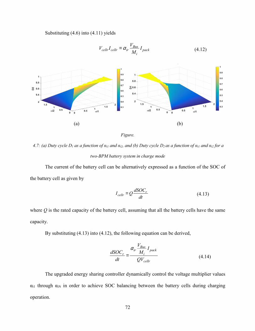
72
Substituting (4.6) into (4.11) yields
Bus
cellr cellr ir packi
VV I I
Mα= (4.12)
(a) (b)
Figure.
4.7: (a) Duty cycle D1 as a function of αi1 and αi2, and (b) Duty cycle D2 as a function of αi1 and αi2 for a
two-BPM battery system in charge mode
The current of the battery cell can be alternatively expressed as a function of the SOC of
the battery cell as given by
r
cellr
dSOCI Q
dt= (4.13)
where Q is the rated capacity of the battery cell, assuming that all the battery cells have the same
capacity.
By substituting (4.13) into (4.12), the following equation can be derived,
Busir pack
ir
cellr
VI
MdSOC
dt QV
α= (4.14)
The upgraded energy sharing controller dynamically control the voltage multiplier values
αi1 through αiN in order to achieve SOC balancing between the battery cells during charging
operation.
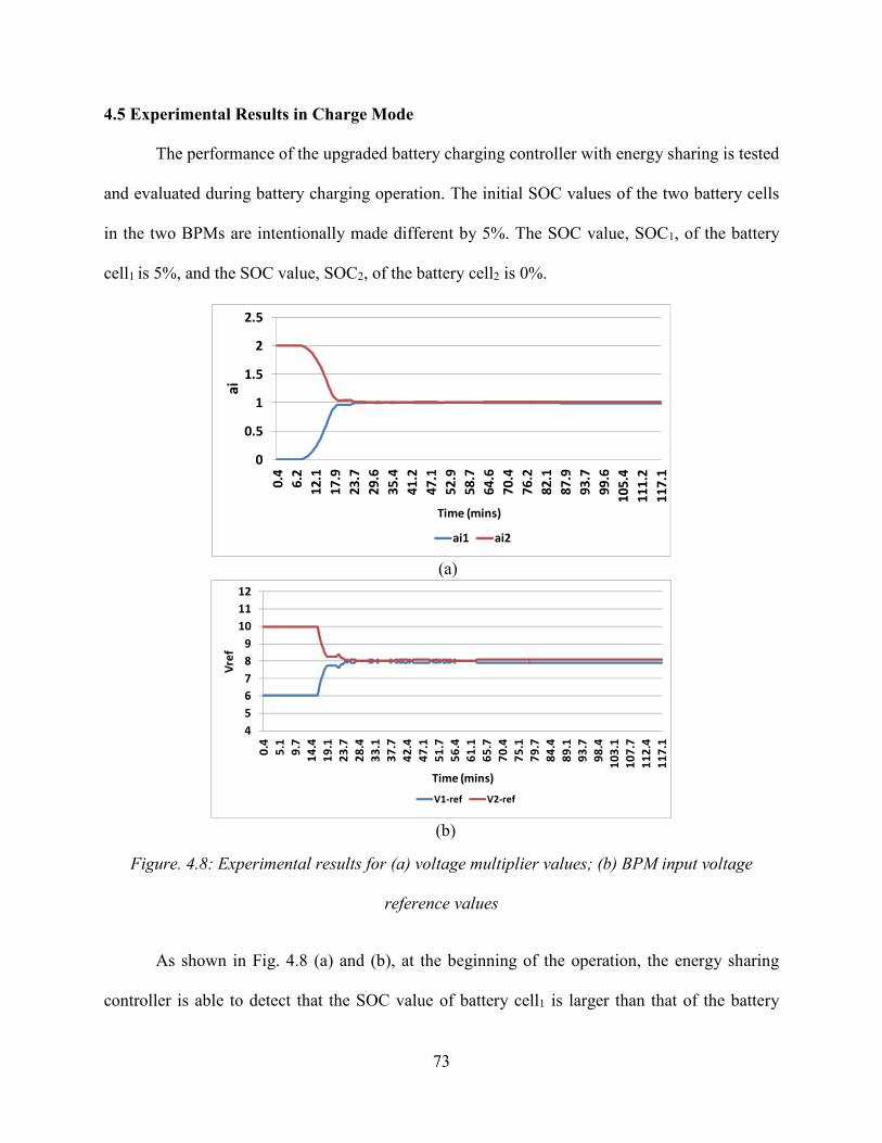
73
4.5 Experimental Results in Charge Mode
The performance of the upgraded battery charging controller with energy sharing is tested
and evaluated during battery charging operation. The initial SOC values of the two battery cells
in the two BPMs are intentionally made different by 5%. The SOC value, SOC1, of the battery
cell1 is 5%, and the SOC value, SOC2, of the battery cell2 is 0%.
0
0.5
1
1.5
2
2.5
0.4
6.2
12
.1
17
.9
23
.7
29
.6
35
.4
41
.2
47
.1
52
.9
58
.7
64
.6
70
.4
76
.2
82
.1
87
.9
93
.7
99
.6
10
5.4
11
1.2
11
7.1
ai
Time (mins)
ai1 ai2
(a)
4
5
6
7
8
9
10
11
12
0.4
5.1
9.7
14
.4
19
.1
23
.7
28
.4
33
.1
37
.7
42
.4
47
.1
51
.7
56
.4
61
.1
65
.7
70
.4
75
.1
79
.7
84
.4
89
.1
93
.7
98
.4
10
3.1
10
7.7
11
2.4
11
7.1
Vre
f
Time (mins)
V1-ref V2-ref
(b)
Figure. 4.8: Experimental results for (a) voltage multiplier values; (b) BPM input voltage
reference values
As shown in Fig. 4.8 (a) and (b), at the beginning of the operation, the energy sharing
controller is able to detect that the SOC value of battery cell1 is larger than that of the battery
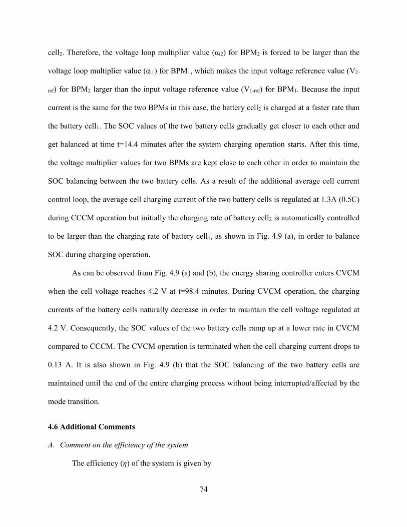
74
cell2. Therefore, the voltage loop multiplier value (αi2) for BPM2 is forced to be larger than the
voltage loop multiplier value (αi1) for BPM1, which makes the input voltage reference value (V2-
ref) for BPM2 larger than the input voltage reference value (V1-ref) for BPM1. Because the input
current is the same for the two BPMs in this case, the battery cell2 is charged at a faster rate than
the battery cell1. The SOC values of the two battery cells gradually get closer to each other and
get balanced at time t=14.4 minutes after the system charging operation starts. After this time,
the voltage multiplier values for two BPMs are kept close to each other in order to maintain the
SOC balancing between the two battery cells. As a result of the additional average cell current
control loop, the average cell charging current of the two battery cells is regulated at 1.3A (0.5C)
during CCCM operation but initially the charging rate of battery cell2 is automatically controlled
to be larger than the charging rate of battery cell1, as shown in Fig. 4.9 (a), in order to balance
SOC during charging operation.
As can be observed from Fig. 4.9 (a) and (b), the energy sharing controller enters CVCM
when the cell voltage reaches 4.2 V at t=98.4 minutes. During CVCM operation, the charging
currents of the battery cells naturally decrease in order to maintain the cell voltage regulated at
4.2 V. Consequently, the SOC values of the two battery cells ramp up at a lower rate in CVCM
compared to CCCM. The CVCM operation is terminated when the cell charging current drops to
0.13 A. It is also shown in Fig. 4.9 (b) that the SOC balancing of the two battery cells are
maintained until the end of the entire charging process without being interrupted/affected by the
mode transition.
4.6 Additional Comments
A. Comment on the efficiency of the system
The efficiency (η) of the system is given by
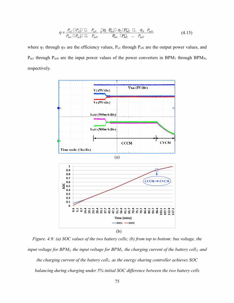
75
1 2 1 1 2 2
1 2 1 2
... ...
... ...o o oN in in N inN
in in inN in in inN
P P P P P P
P P P P P P
η η ηη + + + ⋅ + ⋅ + + ⋅= =+ + + + + +
(4.15)
where η1 through ηN are the efficiency values, Po1 through PoN are the output power values, and
Pin1 through PinN are the input power values of the power converters in BPM1 through BPMN,
respectively.
(a)
0
0.1
0.2
0.3
0.4
0.5
0.6
0.7
0.8
0.9
1
0.4
5.1
9.7
14
.4
19
.1
23
.7
28
.4
33
.1
37
.7
42
.4
47
.1
51
.7
56
.4
61
.1
65
.7
70
.4
75
.1
79
.7
84
.4
89
.1
93
.7
98
.4
10
3.1
10
7.7
11
2.4
11
7.1
SO
C
Time (mins)
SOC1 SOC2
(b)
Figure. 4.9: (a) SOC values of the two battery cells; (b) from top to bottom: bus voltage, the
input voltage for BPM2, the input voltage for BPM1, the charging current of the battery cell2, and
the charging current of the battery cell1, as the energy sharing controller achieves SOC
balancing during charging under 5% initial SOC difference between the two battery cells
76
With an optimized design based on the state-of-art commercially available electronic
devices and PCB layout technique, the bidirectional DC-DC buck/boost converter used in each
BPM can achieve a peak efficiency of 96%-98%, therefore, the overall efficiency η of the
complete system is 96%-98%. Compared to the conventional architecture where there are
independent cell SOC balancing converter across each cell in addition to the high-power DC bus
voltage regulation converter, the proposed architecture is expected to have comparable or higher
efficiency because:
1) Power loss exists in the cell balancing converters in the conventional architecture. This
power loss is caused by the energy transfer between the battery cells in order to achieve cell
balancing. In this work, the same power conversion stage used for voltage regulation is also used
for SOC balancing without the need to add additional SOC balancing circuits or converters for
each cell.
2) High-power-rating devices are needed for the big high-power DC bus voltage
regulation converter in the conventional architecture. Generally speaking, high-power-rating
devices have higher parasitic component values which lead to higher power loss and lower
efficiency than the small low-power converters utilized in this work.
B. Comment on the cost of the system
The cost incurred in the larger high-power DC-DC power converter in the conventional
architecture is replaced by the cost incurred by the smaller lower-power DC-DC power
converters in the distributed architecture. The cost and power loss of the cell balancing circuits or
converters placed across the cells in order to achieve SOC balancing in the conventional
architecture are eliminated when using the energy sharing controller architecture presented in
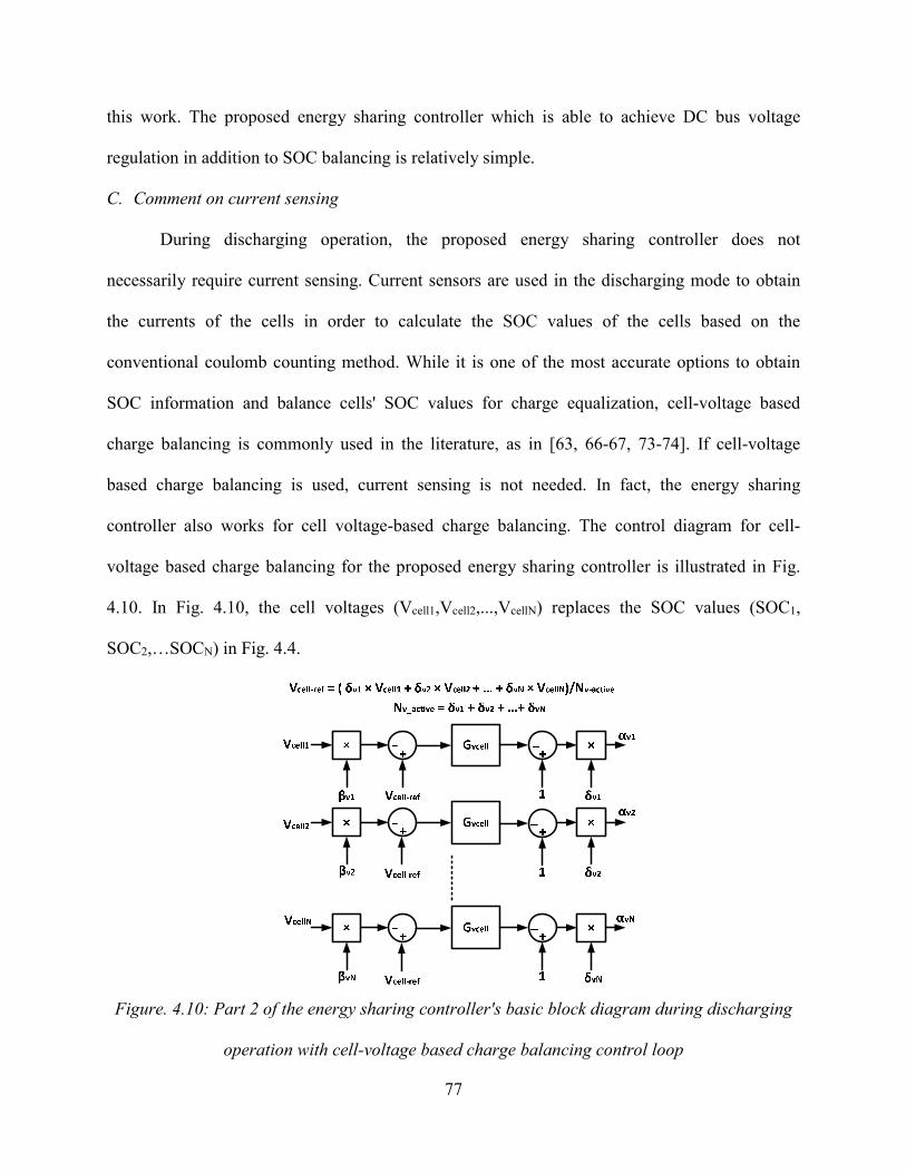
77
this work. The proposed energy sharing controller which is able to achieve DC bus voltage
regulation in addition to SOC balancing is relatively simple.
C. Comment on current sensing
During discharging operation, the proposed energy sharing controller does not
necessarily require current sensing. Current sensors are used in the discharging mode to obtain
the currents of the cells in order to calculate the SOC values of the cells based on the
conventional coulomb counting method. While it is one of the most accurate options to obtain
SOC information and balance cells' SOC values for charge equalization, cell-voltage based
charge balancing is commonly used in the literature, as in [63, 66-67, 73-74]. If cell-voltage
based charge balancing is used, current sensing is not needed. In fact, the energy sharing
controller also works for cell voltage-based charge balancing. The control diagram for cell-
voltage based charge balancing for the proposed energy sharing controller is illustrated in Fig.
4.10. In Fig. 4.10, the cell voltages (Vcell1,Vcell2,...,VcellN) replaces the SOC values (SOC1,
SOC2,…SOCN) in Fig. 4.4.
Figure. 4.10: Part 2 of the energy sharing controller's basic block diagram during discharging
operation with cell-voltage based charge balancing control loop
78
During the charging operation, the proposed energy sharing controller does require
current sensing for the battery cells. However, another option which can be used to reduce
current sensing size and cost is to indirectly sense the current values. Instead of using the
conventional sensing resistor method that results in additional power dissipation and increase in
size and cost, the method that utilizes FET drain-source resistance (Rds(on)) as an indirect way to
sense the current can be utilized [95-96]. In the bidirectional buck/boost converter topology
utilized in this work, two power MOSFETs are used as the switching devices. By measuring the
voltage at the switching node (the point where the two FETs are connected), the current
information can be obtained.
4.7 Summary
The energy sharing controller proposed in last chapter is upgraded in this chapter by
integrating a battery charging control algorithm with the energy sharing concept in order to
address the cell balancing issue during charging operation. The upgraded energy sharing
controller also addresses the battery cells' SOC imbalance issue from the root by adjusting the
charge rate of each battery cell while maintaining the average cell current to be regulated at the
desired level. The energy transfer between the battery cells that is usually required in the
conventional cell balancing schemes is also eliminated. This leads to increased efficiency of the
battery system. The experimental prototype results validate the performance of the upgraded
energy sharing controller during charging operation.
79
CHAPTER 5
SMALL-SIGNAL MODELING AND ENERGY SHARING CONTROLLER DESIGN
5.1 Introduction
An energy sharing controller has been proposed and developed in Chapter 3 to achieve
cell balancing in battery discharge mode with high cell balancing speed and efficiency. The
energy sharing concept is upgraded and integrated with a battery charging algorithm in Chapter 4
in order to achieve cell balancing during battery charging operation. Steady-state operation and
analysis of the energy sharing controller has been presented in Chapter 3 and 4 for discharging
and charging operation, respectively. In order to gain deeper insights into the dynamics of the
energy sharing controlled distributed battery system and facilitate the energy sharing controller
design, detailed small-signal modeling and analysis is performed in this chapter for each
operating mode, i.e., discharge mode, constant current charging mode and constant voltage
charging mode. In each mode, the corresponding small signal model of the system is first
constructed followed by derivation of associated transfer functions. Finally, the control loops
including BPM voltage, SOC balancing, average cell current and average cell voltage loops are
compensated based on rule-of-thumb frequency-domain design guidelines and criteria, i.e.,
control bandwidth and stability margins.
Several different small-signal modeling techniques are introduced and discussed in [97],
including basic AC modeling, state-space averaging, circuit averaging techniques. While the
procedures of each modeling technique may vary, the end results are essentially the same. In this
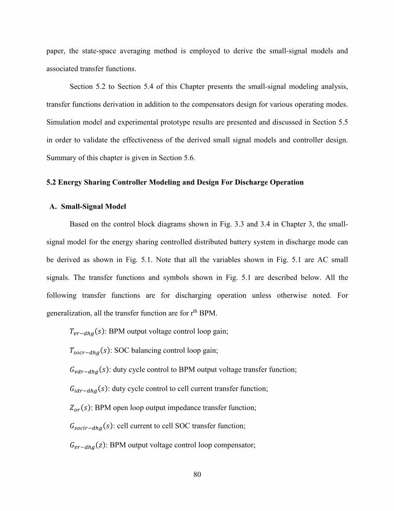
80
paper, the state-space averaging method is employed to derive the small-signal models and
associated transfer functions.
Section 5.2 to Section 5.4 of this Chapter presents the small-signal modeling analysis,
transfer functions derivation in addition to the compensators design for various operating modes.
Simulation model and experimental prototype results are presented and discussed in Section 5.5
in order to validate the effectiveness of the derived small signal models and controller design.
Summary of this chapter is given in Section 5.6.
5.2 Energy Sharing Controller Modeling and Design For Discharge Operation
A. Small-Signal Model
Based on the control block diagrams shown in Fig. 3.3 and 3.4 in Chapter 3, the small-
signal model for the energy sharing controlled distributed battery system in discharge mode can
be derived as shown in Fig. 5.1. Note that all the variables shown in Fig. 5.1 are AC small
signals. The transfer functions and symbols shown in Fig. 5.1 are described below. All the
following transfer functions are for discharging operation unless otherwise noted. For
generalization, all the transfer function are for rth BPM.
: BPM output voltage control loop gain;
@: SOC balancing control loop gain;
: duty cycle control to BPM output voltage transfer function;
A: duty cycle control to cell current transfer function;
B: BPM open loop output impedance transfer function;
@A: cell current to cell SOC transfer function;
: BPM output voltage control loop compensator;
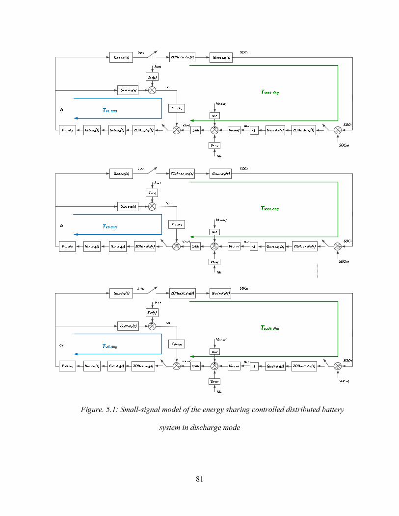
81
Figure. 5.1: Small-signal model of the energy sharing controlled distributed battery
system in discharge mode
82
@: SOC balancing control loop compensator;
C: BPM output voltage sensing gain (including the voltage sensor gain and the
analog-to-digital converter gain);
: PWM modulator gain;
>: digital controller computation delay model;
B7>: zero order hold model for BPM output voltage sampling;
B7>A*++: zero order hold model for cell current sampling;
B7>@: zero order hold model for cell SOC sampling;
The converter design parameters and equilibrium operating point (when the battery cells
are balanced) are the same for all the BPMs. Therefore, the compensators design for all the
BPMs are identical. The following section presents the derivation of the transfer functions for rth
BPM during discharging operation.
B. Derivation of Transfer Functions
In discharge mode, the BPM converters operate in boost mode with the battery cells
being the inputs as shown in Fig. 5.2. The independent state variables of a BPM converter in this
mode are the inductor current or cell current icell(t) and the BPM converter output voltage v(t).
The input variables are cell open circuit voltage Voc(t) and output current or battery pack current
ipack(t). The output variables are the same as the state variables.
Next, the state equations for rth BPM during each subinterval are derived from Fig. 5.2. When
Slr is on and Sur is off during drTs time duration, the state equations are
DE AFGHH;II = JK − M*++K ∙ B*++8 ;II = −M=OK (5.1)
83
where dr is the duty cycle and Ts is the switching period of the BPM converter. Other variables
are as defined in Fig. 5.2. When Sur is on and Slr is off during (1-dr)Ts time duration, the state
equation is given by
DE AFGHH;II = JK − M*++K ∙ B*++ − JK8 ;II = M*++K − M=OK (5.2)
Equations (5.1) and (5.2) can be rewritten in the following state-space form:
C PII = QRSK + URVK (5.3)
C PII = QWSK + UWVK (5.4)
Where C = XE 00 8Z , Q1 = X−B*++ 00 0Z , U1 = X1 00 −1Z , Q2 = X−B*++ −11 0 Z , U2 = X1 00 −1Z, SK = XAFGHH;I;I Z, and VK = ^ _F;IA`?FaIb.
The next step is to evaluate the state-space averaged equilibrium equations. The averaged
matrix A is
Q = cQ1 + cdQ2 = c X−B*++ 00 0Z + cd X−B*++ −11 0 Z = ^−B*++ −cdcd 0 b (5.5)
where Dr'=1-Dr
Figure. 5.2: Circuit diagram of the BPM operating as a boost converter in discharge mode
Similarly, the averaged matrix B is
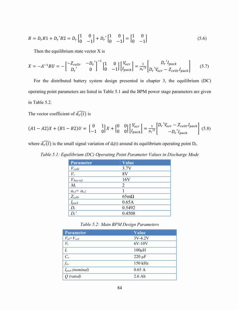
84
U = cU1 + cdU2 = c X1 00 −1Z + cd X1 00 −1Z = X1 00 −1Z (5.6)
Then the equilibrium state vector X is
e = −QRUf = − ^−B*++ −cdcd 0 bR X1 00 −1Z ^ gh=Ob = Ri;jk l cdh=Ocdg − B*++h=Om (5.7)
For the distributed battery system design presented in chapter 3, the equilibrium (DC)
operating point parameters are listed in Table 5.1 and the BPM power stage parameters are given
in Table 5.2.
The vector coefficient of nKo is
Q1 − Q2e + U1 − U2f = X 0 1−1 0Z e + X0 00 0Z ^ gh=Ob = Ri;jk lcdg − B*++h=O−cdh=O m (5.8)
where nKo is the small signal variation of dr(t) around its equilibrium operating point Dr.
Table 5.1: Equilibrium (DC) Operating Point Parameter Values in Discharge Mode
Parameter Value
Vcellr 3.7V
Vr 8V
Vbus-ref 16V
Mv 2
αv1= αv2 1
Zcellr 65mΩ
Ipack 0.65A
Dr 0.5492
Dr' 0.4508
Table 5.2: Main BPM Design Parameters
Parameter Value
Vin=Vcell 3V-4.2V
Vr 6V-10V
L 100µH
Co 220 µF
fsw 150 kHz
Ipack (nominal) 0.65 A
Q (rated) 2.6 Ah
85
The small-signal AC state equations therefore become
XE 00 8Z nnK lp*++KoJKo m = ^−B*++ −cdcd 0 b lp*++KoJKo m
+ X1 00 −1Z l JKop=OKo m + Ri;jk lcdg − B*++h=O−cdh=O m nKo (5.9) When written in scalar from, (5.9) becomes
qrsrtE uFGHH;IoI = −B*++p*++Ko − cdJKo + JKo
+ Ri;jk cdgnKo − B*++h=OnKo8 ;IoI = cdp*++Ko − p=OKo − v`?Fai;j nKo
(5.10)
Since the dynamics of the cell open circuit voltage variation JKo is very slow compared to
the dynamics of the BPM converter, it can be assumed that the AC small signal variation of the
cell open circuit voltage around its equilibrium point is 0, i.e., JKo =0. Based on this,
performing Laplace Transformation on (5.10) yields
qrsrtEM*++ = −B*++M*++ − cdJ + Ri;jk cdgn−B*++h=On8J = cdM*++ − M=O − Ri;j h=On (5.11)
where s is the Laplace Transform operator (s=jω). Let the small signal variation of independent
variable M=O = 0 and simplify (5.11) yields
qrsrtEM*++ = −B*++M*++ − cdJ + Ri;jk cdgn−B*++h=On8J = cdM*++ − Ri;j h=On (5.12)
Based on (5.12), the following transfer functions can be derived
= @@ = %wxyFGHH;z`?Fa;j x |;ji;j_F;yFGHH;v`?Fa%wxyFGHH;%'xi;jk (5.13)
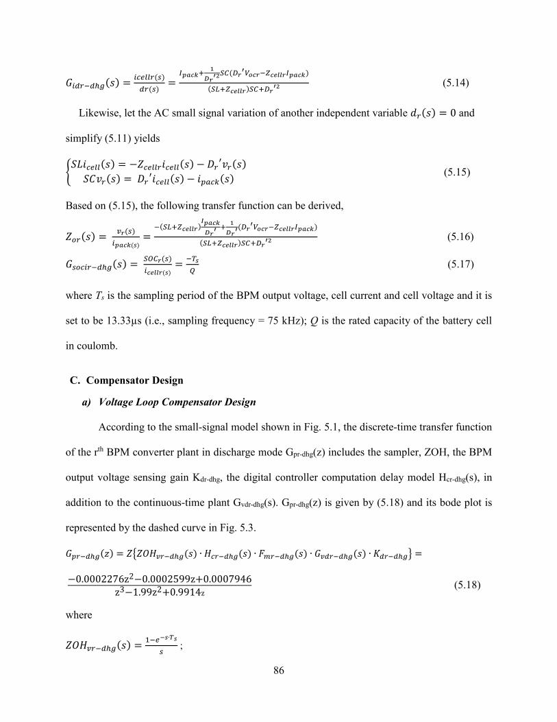
86
A = A*++@@ = v`?Fax |;jk%'i;j_F;yFGHH;v`?Fa%wxyFGHH;%'xi;jk (5.14)
Likewise, let the AC small signal variation of another independent variable n = 0 and
simplify (5.11) yields
~6EM*++ = −B*++M*++ − cdJ68J = cdM*++ − M=O (5.15)
Based on (5.15), the following transfer function can be derived,
B = ;@A`?Fa = %wxyFGHH;z`?Fa;j x |;ji;j_F;yFGHH;v`?Fa%wxyFGHH;%'xi;jk (5.16)
@A = %&';@AFGHH; = : (5.17)
where Ts is the sampling period of the BPM output voltage, cell current and cell voltage and it is
set to be 13.33µs (i.e., sampling frequency = 75 kHz); Q is the rated capacity of the battery cell
in coulomb.
C. Compensator Design
a) Voltage Loop Compensator Design
According to the small-signal model shown in Fig. 5.1, the discrete-time transfer function
of the rth BPM converter plant in discharge mode Gpr-dhg(z) includes the sampler, ZOH, the BPM
output voltage sensing gain Kdr-dhg, the digital controller computation delay model Hcr-dhg(s), in
addition to the continuous-time plant Gvdr-dhg(s). Gpr-dhg(z) is given by (5.18) and its bode plot is
represented by the dashed curve in Fig. 5.3.
= BB7> ∙ > ∙ ∙ ∙ C = −0.0002276z2−0.0002599z+0.0007946z3−1.99z2+0.9914z (5.18)
where
B7> = R*∙@ ;
87
> = @∙ ; Td is the digital controller computation delay and it is equal to Td = 1.5Tsw
in the experimental implementation;
= RRW ; C = 11.13.
Figure. 5.3: The bode plot of the uncompensated (dashed curve) and compensated (solid curve)
BPM output voltage control loop gain in discharge mode
In this voltage control loop design, the target control bandwidth is limited by the right-
half-plane (RHP) zero located at 3.87 kHz, as can be observed from the dashed curve in Fig. 5.3.
With a compensator Gvr-dhg(z) given by (5.19), the compensated BPM output voltage control loop
gain (Tvr-dhg(z) = Gpr-dhg(z)⋅Gvr-dhg(z)) achieves a control bandwidth of 1.53 kHz and a phase
margin of 35.5°, as shown on the solid curve in Fig. 5.3.
= ..kR.x.R (5.19)
b) SOC Balancing Loop Compensator Design
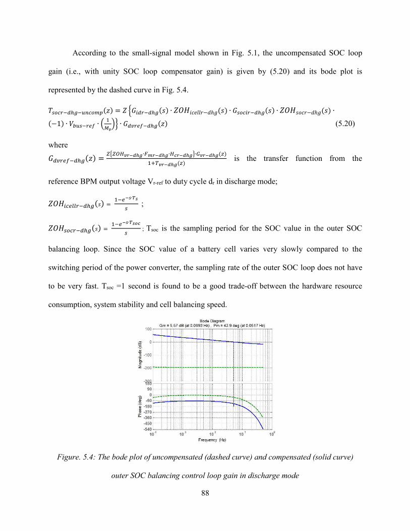
88
According to the small-signal model shown in Fig. 5.1, the uncompensated SOC loop
gain (i.e., with unity SOC loop compensator gain) is given by (5.20) and its bode plot is
represented by the dashed curve in Fig. 5.4.
@ = B A ∙ B7>M−nℎ ∙ @A ∙ B7>−nℎ ∙−1 ∙ g @* ∙ R ¡¢£ ∙ * (5.20)
where * = yy&¤¡;¥¦∙§¨;¥¦∙¤F;¥¦∙©¡;¥¦ªRx¡;¥¦ª is the transfer function from the
reference BPM output voltage Vr-ref to duty cycle dr in discharge mode;
B7>A*++ = R*∙@ ; B7>@ = R*∙_F@ ; Tsoc is the sampling period for the SOC value in the outer SOC
balancing loop. Since the SOC value of a battery cell varies very slowly compared to the
switching period of the power converter, the sampling rate of the outer SOC loop does not have
to be very fast. Tsoc =1 second is found to be a good trade-off between the hardware resource
consumption, system stability and cell balancing speed.
Figure. 5.4: The bode plot of uncompensated (dashed curve) and compensated (solid curve)
outer SOC balancing control loop gain in discharge mode
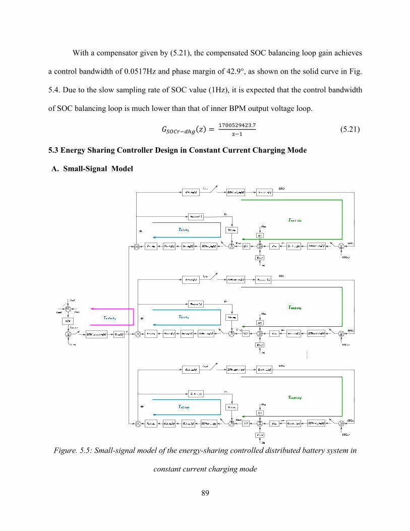
89
With a compensator given by (5.21), the compensated SOC balancing loop gain achieves
a control bandwidth of 0.0517Hz and phase margin of 42.9°, as shown on the solid curve in Fig.
5.4. Due to the slow sampling rate of SOC value (1Hz), it is expected that the control bandwidth
of SOC balancing loop is much lower than that of inner BPM output voltage loop.
%&' = RWW«.R (5.21)
5.3 Energy Sharing Controller Design in Constant Current Charging Mode
A. Small-Signal Model
Figure. 5.5: Small-signal model of the energy-sharing controlled distributed battery system in
constant current charging mode
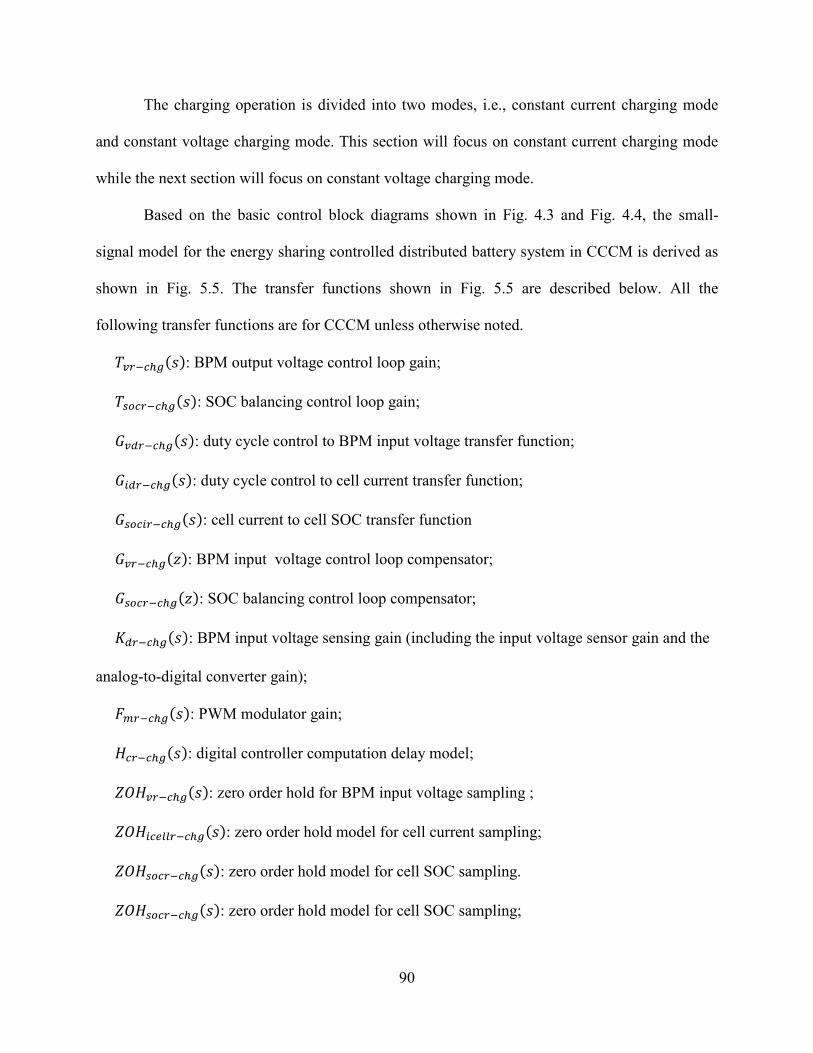
90
The charging operation is divided into two modes, i.e., constant current charging mode
and constant voltage charging mode. This section will focus on constant current charging mode
while the next section will focus on constant voltage charging mode.
Based on the basic control block diagrams shown in Fig. 4.3 and Fig. 4.4, the small-
signal model for the energy sharing controlled distributed battery system in CCCM is derived as
shown in Fig. 5.5. The transfer functions shown in Fig. 5.5 are described below. All the
following transfer functions are for CCCM unless otherwise noted.
: BPM output voltage control loop gain;
@: SOC balancing control loop gain;
: duty cycle control to BPM input voltage transfer function;
A: duty cycle control to cell current transfer function;
@A: cell current to cell SOC transfer function
: BPM input voltage control loop compensator;
@: SOC balancing control loop compensator;
C: BPM input voltage sensing gain (including the input voltage sensor gain and the
analog-to-digital converter gain);
: PWM modulator gain;
>: digital controller computation delay model;
B7>: zero order hold for BPM input voltage sampling ;
B7>A*++: zero order hold model for cell current sampling;
B7>@: zero order hold model for cell SOC sampling.
B7>@: zero order hold model for cell SOC sampling;
91
B7>A*++=: zero order hold model for average cell current sampling.
Each BPM still consists of two independent control loops, i.e., BPM converter input
voltage control loop and SOC control loop. In addition, all BPMs share an average cell current
control loop. The following section presents derivation of the transfer functions associated with
each control loop in CCCM.
Figure. 5.6: Circuit diagram of rth BPM operating as a buck converter in charge mode
B. Derivation of Transfer Functions
During charging operation, the converters operate as buck converters with the cells being
the outputs as shown in Fig. 5.6. The independent state variables of each BPM converter in this
case are the inductor current or cell current icell(t) and the BPM input voltage v(t). The input
variables are cell open circuit voltage Voc(t) and input current or pack current ipack(t). The output
variables are the same as the state variables.
Next, the state equations for rth BPM during each subinterval are derived. When Sur is on and
Slr is off during drTs time duration, the state equations are
DE AFGHH;II = JK − M*++K ∙ B*++ − JK8 ;II = M=OK − M*++K (5.22)
When Slr is on and Sur is off during (1-dr)Ts time duration:
DE AFGHH;II = −M*++K ∙ B*++ − JK8 ;II = M=OK (5.23)
92
Equations (5.22) and (5.23) can be rewritten in the following state-space form: C PII = QRSK + URVK (5.24)
C PII = QWSK + UWVK (5.25)
Where ¬ = XE 00 8Z, SK = XAFGHH;I;I Z , VK = ^ _F;IA`?FaIb,Q1 = X−B*++ 1−1 0Z , U1 = X−1 00 1Z , Q2 = X−B*++ 00 0Z , ®n U2 = X−1 00 1Z
The next step is to evaluate the state-space averaged equilibrium equations. The averaged
matrix A is
Q = cQ1 + cdQ2 = c X−B*++ 1−1 0Z + cd X−B*++ 00 0Z = ^−B*++ c−c 0 b (5.26)
Similarly, the averaged matrix B is
U = cU1 + cdU2 = c X−1 00 1Z + cd X−1 00 1Z = X−1 00 1Z (5.27)
Therefore, the equilibrium state vector X is
e = −QRUf = − ^−B*++ c−c 0 bR X−1 00 1Z ^ gh=Ob = ¯ v`?Fai;_F;i; + yFGHH;i;k h=O° (5.28)
The equilibrium operating point parameters used in the charge mode are listed in Table 5.3.
Table 5.3: Equilibrium Operating Point Parameter Values in Charge Mode
Parameter Value
Vcellr 3.7V
Vr 8V
Vbus 16V
Mi 2
αi1= αi2 1
Zcellr 65mΩ
Icell-ref 1.3A
Ipack 0.615A
Dr 0.4731
Dr' 0.5269
The vector coefficient of nKo is
93
Q1 − Q2e + U1 − U2f = X 0 1−1 0Z e + X0 00 0Z ^ gh=Ob = ¯_F;i; + yFGHH;i;k h=O− v`?Fai;° (5.29)
The small-signal AC state equations therefore become
XE 00 8Z I lp*++KoJKo m = ^−B*++ c−c 0 b lp*++KoJKo m + X−1 00 1Z l JKop=OKo m +¯_F;i; + yFGHH;i;k h=O− v`?Fai;
° nKo (5.30)
When written in scalar from, (5.30) becomes
qrsrtE uFGHH;IoI = −B*++p*++Ko + cJKo − JKo
+_F;i; + yFGHH;i;k h=OnKo 8 ;IoI = −cp*++Ko + p=OKo − v`?Fai; nKo
(5.31)
Again, it is assumed that JKo =0 here. Then performing Laplace Transform on (5.31) yields
D6EM*++ = −B*++M*++ + cJ + _F;i; + yFGHH;i;k h=On68J = −cM*++ + M=O − v`?Fai; n (5.32)
Let the AC small signal variation of another independent variable M=O = 0 and simplify
(5.32) yields
D6EM*++ = −B*++M*++ + cJ + _F;i; + yFGHH;i;k h=On68J = −cM*++ − v`?Fai; n (5.33)
Based on (5.33), the following transfer functions can be derived,
= @@ = %wxyFGHHz`?Fa; _F;x±FGHH; v`?Fa%wxyFGHH%'xi;k (5.34)
A = A*++@@ = v`?Fax%'²_F;; x±FGHH;k v`?Fa%wxyFGHH%'xi;k (5.35)
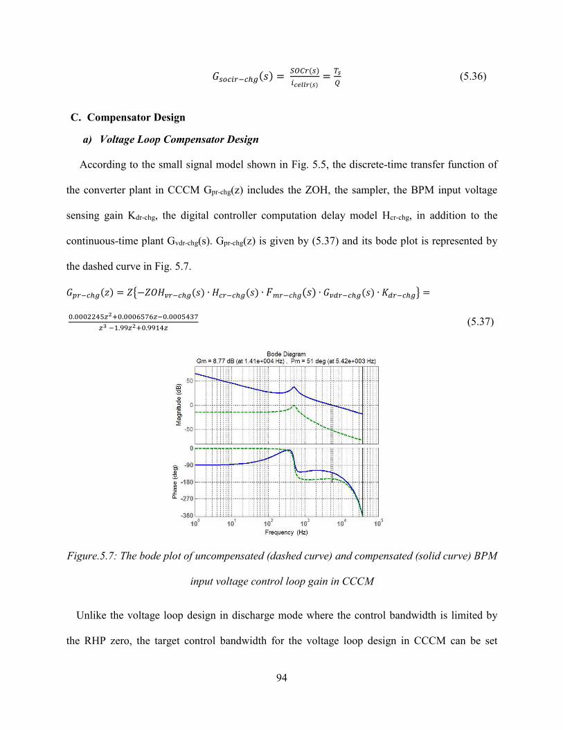
94
@A = %&'@AFGHH; = : (5.36)
C. Compensator Design
a) Voltage Loop Compensator Design
According to the small signal model shown in Fig. 5.5, the discrete-time transfer function of
the converter plant in CCCM Gpr-chg(z) includes the ZOH, the sampler, the BPM input voltage
sensing gain Kdr-chg, the digital controller computation delay model Hcr-chg, in addition to the
continuous-time plant Gvdr-chg(s). Gpr-chg(z) is given by (5.37) and its bode plot is represented by
the dashed curve in Fig. 5.7.
= B−B7> ∙ > ∙ ³−ℎ ∙ ∙ C = .WWªkx.ª.«ª´ R.ªkx.Rª (5.37)
Figure.5.7: The bode plot of uncompensated (dashed curve) and compensated (solid curve) BPM
input voltage control loop gain in CCCM
Unlike the voltage loop design in discharge mode where the control bandwidth is limited by
the RHP zero, the target control bandwidth for the voltage loop design in CCCM can be set
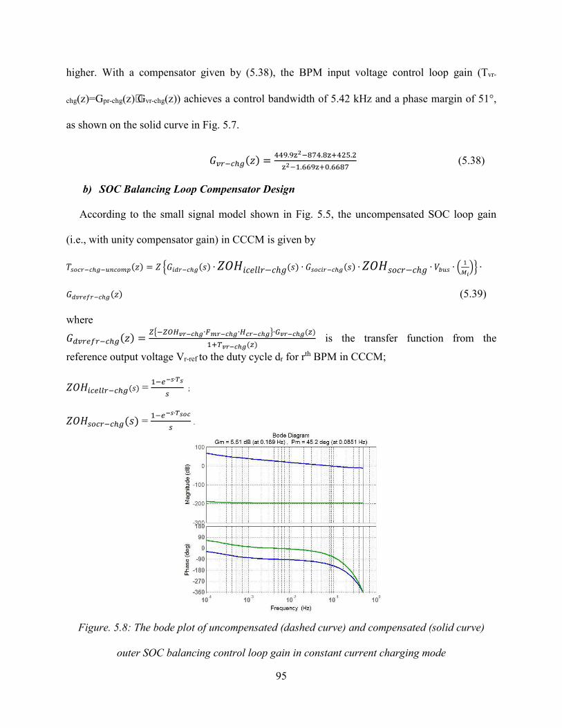
95
higher. With a compensator given by (5.38), the BPM input voltage control loop gain (Tvr-
chg(z)=Gpr-chg(z)⋅Gvr-chg(z)) achieves a control bandwidth of 5.42 kHz and a phase margin of 51°,
as shown on the solid curve in Fig. 5.7.
= .kµ.µxW.WkR.x.µ (5.38)
b) SOC Balancing Loop Compensator Design
According to the small signal model shown in Fig. 5.5, the uncompensated SOC loop gain
(i.e., with unity compensator gain) in CCCM is given by
@ = B A ∙ B7>M−ℎ ∙ @A ∙ B7>−ℎ ∙ g @ ∙ R ¶¢£ ∙* (5.39)
where * = yy&¤¡;F¥¦∙§¨;F¥¦∙¤F;F¥¦∙©¡;F¥¦ªRx¡;F¥¦ª is the transfer function from the
reference output voltage Vr-ref to the duty cycle dr for rth BPM in CCCM; B7>A*++ =
R*∙@ ; B7>@ =
R*∙_F@ .
Figure. 5.8: The bode plot of uncompensated (dashed curve) and compensated (solid curve)
outer SOC balancing control loop gain in constant current charging mode
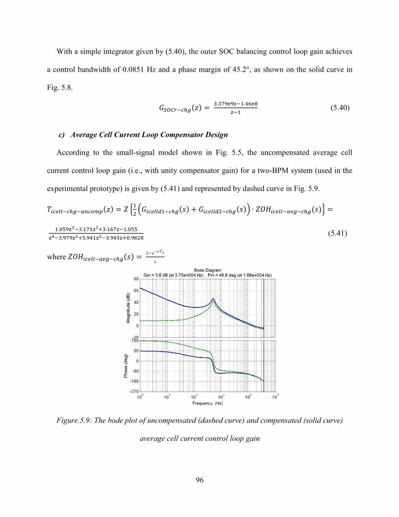
96
With a simple integrator given by (5.40), the outer SOC balancing control loop gain achieves
a control bandwidth of 0.0851 Hz and a phase margin of 45.2°, as shown on the solid curve in
Fig. 5.8.
%&' = «.«·R.·µR (5.40)
c) Average Cell Current Loop Compensator Design
According to the small-signal model shown in Fig. 5.5, the uncompensated average cell
current control loop gain (i.e., with unity compensator gain) for a two-BPM system (used in the
experimental prototype) is given by (5.41) and represented by dashed curve in Fig. 5.9.
A*++ = B RW A*++R + A*++W¢ ∙ B7>A*++=£ = R.´«.RRkx«.RR.¸«.´x.Rk«.x.µWµ (5.41)
where B7>A*++= = 1−−∙
Figure.5.9: The bode plot of uncompensated (dashed curve) and compensated (solid curve)
average cell current control loop gain
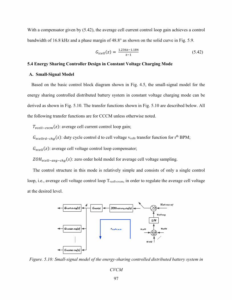
97
With a compensator given by (5.42), the average cell current control loop gain achieves a control
bandwidth of 16.8 kHz and a phase margin of 48.8° as shown on the solid curve in Fig. 5.9.
A*++ = R.W«R.RµR (5.42)
5.4 Energy Sharing Controller Design in Constant Voltage Charging Mode
A. Small-Signal Model
Based on the basic control block diagram shown in Fig. 4.5, the small-signal model for the
energy sharing controlled distributed battery system in constant voltage charging mode can be
derived as shown in Fig. 5.10. The transfer functions shown in Fig. 5.10 are described below. All
the following transfer functions are for CCCM unless otherwise noted.
*++: average cell current control loop gain;
*++: duty cycle control d to cell voltage vcellr transfer function for rth BPM;
*++: average cell voltage control loop compensator;
B7>*++=: zero order hold model for average cell voltage sampling.
The control structure in this mode is relatively simple and consists of only a single control
loop, i.e., average cell voltage control loop Tvcell-cvcm, in order to regulate the average cell voltage
at the desired level.
Figure. 5.10: Small-signal model of the energy-sharing controlled distributed battery system in
CVCM
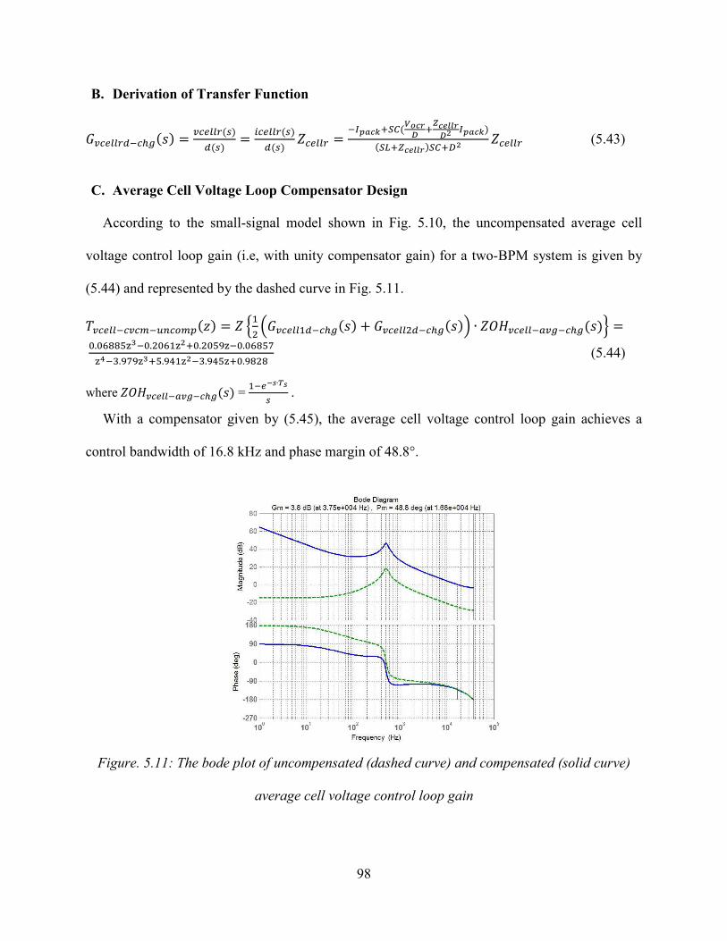
98
B. Derivation of Transfer Function
*++ = *++@@ = A*++@@ B*++ = v`?Fax%'²_F; x±FGHH;k v`?Fa%wxyFGHH;%'xik B*++ (5.43)
C. Average Cell Voltage Loop Compensator Design
According to the small-signal model shown in Fig. 5.10, the uncompensated average cell
voltage control loop gain (i.e, with unity compensator gain) for a two-BPM system is given by
(5.44) and represented by the dashed curve in Fig. 5.11.
*++ = B RW *++R + *++W¢ ∙ B7>*++=£ = .µµ´.WRkx.W.µ¸«.´x.Rk«.x.µWµ (5.44)
where B7>*++= = R*∙@ .
With a compensator given by (5.45), the average cell voltage control loop gain achieves a
control bandwidth of 16.8 kHz and phase margin of 48.8°.
Figure. 5.11: The bode plot of uncompensated (dashed curve) and compensated (solid curve)
average cell voltage control loop gain
99
*++ = R.WRµ.WWR (5.45)
5.5 Simulation and Experimental Model Validation
The derived small-signal models and designed compensators for different operating modes
are validated using both simulation model and experimental prototype results. The simulation
model (based on the derived transfer functions used in a mathematical block diagram based
system model) built in MATLAB®/SIMULIK software package. The designed compensators for
different control loops are implemented by using TMS320S28335 microcontroller and tested on
a two-cell distributed battery system prototype. The design parameters of the simulation model
and experimental prototype are the same and they are as listed in Table 5.2. The simulation and
experimental results are shown in Fig. 5.12 through Fig. 5.13 for discharging operation and in
Fig. 5.14 through Fig. 5.15 for charging operation.
It might be of importance to note that the MATLAB®/SIMULIK simulation model utilizes
the derived small-signal transfer functions equations and compensators obtained in this paper.
Therefore, if the resulted system dynamic responses from the experimental hardware match the
dynamic responses obtained from the MATLAB®/SIMULIK simulation model, this implies that
the developed small-signal model and compensators in this paper are valid.
The performance of the inner BPM output voltage control loop is first tested by disabling the
SOC control loop in the discharge mode. The voltage loop multipliers (αv1 and αv2) are initially
set to be equal to 1 which results in V1-ref = V2-ref = 8V. Then the voltage loop multiplier values
are varied against each other with αv1 being initially set to the minimum value 0 while αv2 is
initially set to the maximum value 2. This leads to V1-ref = 6V and V2-ref=10V. As shown in Fig.
5.12, the simulation model results and the experimental results for each BPM output voltage
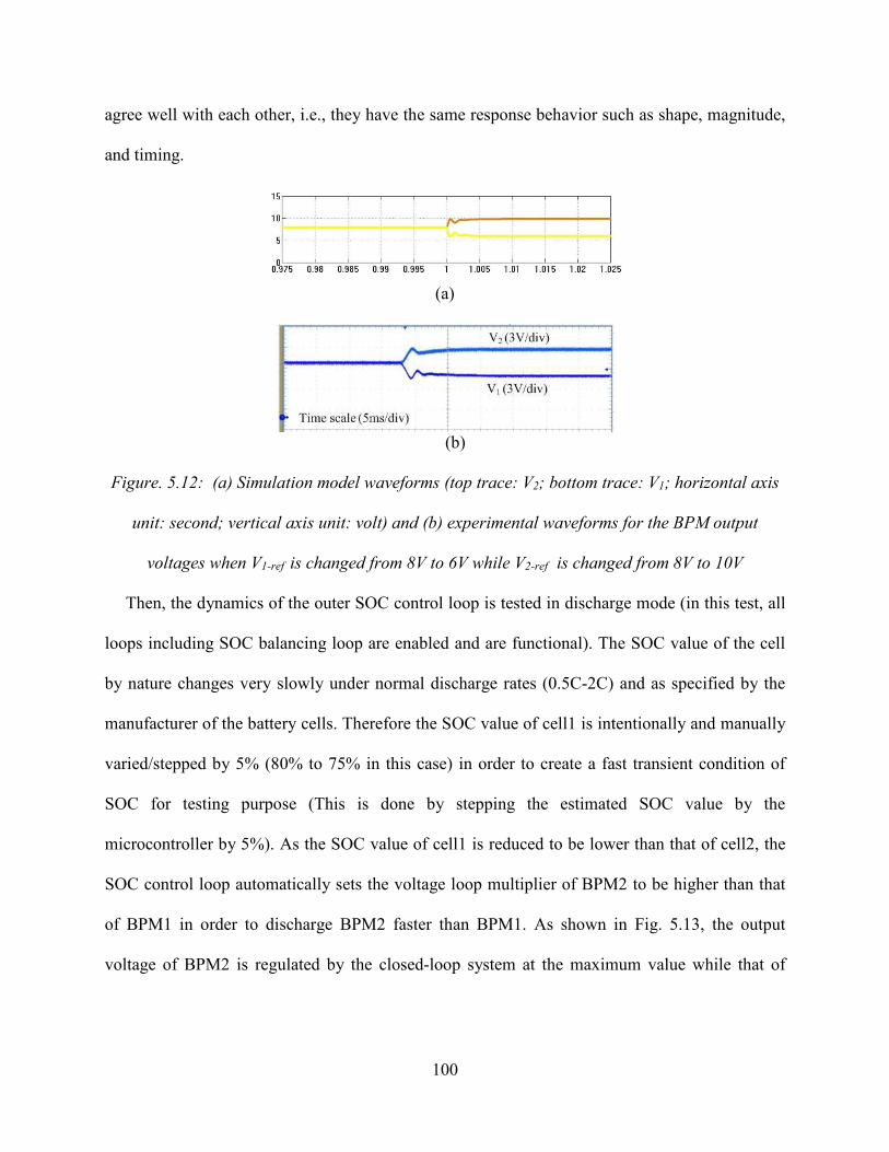
100
agree well with each other, i.e., they have the same response behavior such as shape, magnitude,
and timing.
(a)
(b)
Figure. 5.12: (a) Simulation model waveforms (top trace: V2; bottom trace: V1; horizontal axis
unit: second; vertical axis unit: volt) and (b) experimental waveforms for the BPM output
voltages when V1-ref is changed from 8V to 6V while V2-ref is changed from 8V to 10V
Then, the dynamics of the outer SOC control loop is tested in discharge mode (in this test, all
loops including SOC balancing loop are enabled and are functional). The SOC value of the cell
by nature changes very slowly under normal discharge rates (0.5C-2C) and as specified by the
manufacturer of the battery cells. Therefore the SOC value of cell1 is intentionally and manually
varied/stepped by 5% (80% to 75% in this case) in order to create a fast transient condition of
SOC for testing purpose (This is done by stepping the estimated SOC value by the
microcontroller by 5%). As the SOC value of cell1 is reduced to be lower than that of cell2, the
SOC control loop automatically sets the voltage loop multiplier of BPM2 to be higher than that
of BPM1 in order to discharge BPM2 faster than BPM1. As shown in Fig. 5.13, the output
voltage of BPM2 is regulated by the closed-loop system at the maximum value while that of
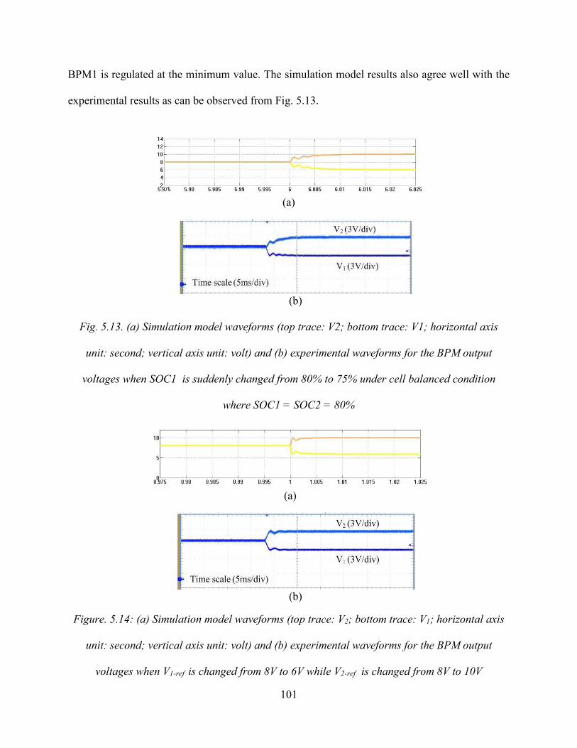
101
BPM1 is regulated at the minimum value. The simulation model results also agree well with the
experimental results as can be observed from Fig. 5.13.
(a)
(b)
Fig. 5.13. (a) Simulation model waveforms (top trace: V2; bottom trace: V1; horizontal axis
unit: second; vertical axis unit: volt) and (b) experimental waveforms for the BPM output
voltages when SOC1 is suddenly changed from 80% to 75% under cell balanced condition
where SOC1 = SOC2 = 80%
(a)
(b)
Figure. 5.14: (a) Simulation model waveforms (top trace: V2; bottom trace: V1; horizontal axis
unit: second; vertical axis unit: volt) and (b) experimental waveforms for the BPM output
voltages when V1-ref is changed from 8V to 6V while V2-ref is changed from 8V to 10V
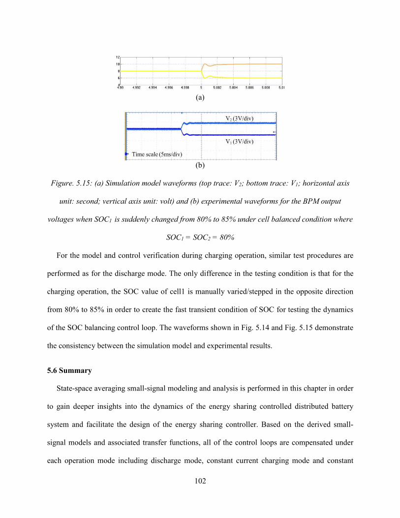
102
(a)
(b)
Figure. 5.15: (a) Simulation model waveforms (top trace: V2; bottom trace: V1; horizontal axis
unit: second; vertical axis unit: volt) and (b) experimental waveforms for the BPM output
voltages when SOC1 is suddenly changed from 80% to 85% under cell balanced condition where
SOC1 = SOC2 = 80%
For the model and control verification during charging operation, similar test procedures are
performed as for the discharge mode. The only difference in the testing condition is that for the
charging operation, the SOC value of cell1 is manually varied/stepped in the opposite direction
from 80% to 85% in order to create the fast transient condition of SOC for testing the dynamics
of the SOC balancing control loop. The waveforms shown in Fig. 5.14 and Fig. 5.15 demonstrate
the consistency between the simulation model and experimental results.
5.6 Summary
State-space averaging small-signal modeling and analysis is performed in this chapter in order
to gain deeper insights into the dynamics of the energy sharing controlled distributed battery
system and facilitate the design of the energy sharing controller. Based on the derived small-
signal models and associated transfer functions, all of the control loops are compensated under
each operation mode including discharge mode, constant current charging mode and constant

103
voltage charging mode by using rule-of-thumb frequency-domain design guidelines and criteria,
such as control bandwidth and stability margins. The derived models and compensators design
are validated by both simulations and experiments on a two-cell distributed battery system
prototype.
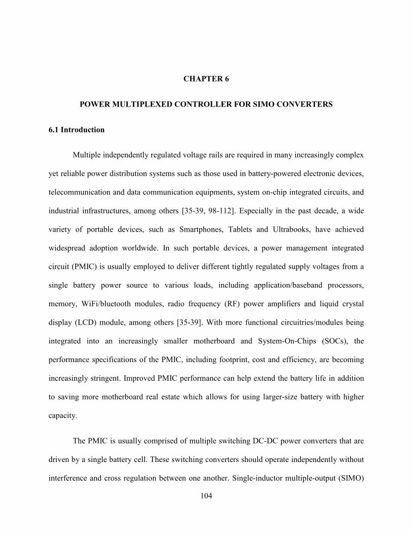
104
CHAPTER 6
POWER MULTIPLEXED CONTROLLER FOR SIMO CONVERTERS
6.1 Introduction
Multiple independently regulated voltage rails are required in many increasingly complex
yet reliable power distribution systems such as those used in battery-powered electronic devices,
telecommunication and data communication equipments, system on-chip integrated circuits, and
industrial infrastructures, among others [35-39, 98-112]. Especially in the past decade, a wide
variety of portable devices, such as Smartphones, Tablets and Ultrabooks, have achieved
widespread adoption worldwide. In such portable devices, a power management integrated
circuit (PMIC) is usually employed to deliver different tightly regulated supply voltages from a
single battery power source to various loads, including application/baseband processors,
memory, WiFi/bluetooth modules, radio frequency (RF) power amplifiers and liquid crystal
display (LCD) module, among others [35-39]. With more functional circuitries/modules being
integrated into an increasingly smaller motherboard and System-On-Chips (SOCs), the
performance specifications of the PMIC, including footprint, cost and efficiency, are becoming
increasingly stringent. Improved PMIC performance can help extend the battery life in addition
to saving more motherboard real estate which allows for using larger-size battery with higher
capacity.
The PMIC is usually comprised of multiple switching DC-DC power converters that are
driven by a single battery cell. These switching converters should operate independently without
interference and cross regulation between one another. Single-inductor multiple-output (SIMO)
105
switching converter is a cost-effective alternative solution to the multiple individual switching
converters architecture. By using only a single power inductor and/or less power switching
devices, SIMO converter can potentially lead to reduced size, cost, component count in addition
to eliminating mutual coupling between the power inductors which are closely integrated on a
high-density board or chip [35-39]. However, due to the fact that the multiple output voltage rails
are coupled to the same switching node in a SIMO converter, the cross regulation between the
outputs can severely degrade the output voltage regulation performance during steady-state and
dynamic operations and may even cause system instability in a worst case scenario.
This cross regulation effect has been extensively studied in the literature as in [35-39, 98-
106] and a number of control schemes have been proposed aiming to address this issue. For
example, in [35], a time-multiplexed control scheme is proposed to suppress the cross regulation
between the outputs in boost or buck-boost derived SIMO converter operating in discontinuous
conduction mode (DCM). This control scheme, however, is not well suited for the buck-derived
SIMO converter where the switches are located at the input side instead of the output. Moreover,
the controller presented in [35] is only suitable for DCM operation. When the SIMO converter
enters continuous conduction mode (CCM) at heavy loads, this controller is no longer effective
because the variation of the voltage/current in one output will directly affect the amount of
energy delivered to other outputs, thus causing cross regulation. To suppress the cross regulation
of the SIMO converter in CCM, a modified control scheme is proposed in [36] where a dc offset
current is introduced in order to initialize the inductor current to the same value at the beginning
of each switching cycle. This concept results in reduced cross regulation in CCM while
maintaining low inductor current and output voltage ripples for higher efficiency and lower
switching noise. The downside of this concept, however, is that it requires an extra freewheel
106
switch and current sensing circuitries in addition to a sophisticated technique to determine the
optimal dc offset current value under different load current conditions. In [37], a predictive
digital current mode controller is proposed, where the duty cycle value for each switch in the
SIMO converter is calculated based on the current reference value and the estimated inductor
current. While resulting in reduced cross regulation, this controller requires fairly high
computational capabilities and resources. A state feedback control mechanism is presented in
[38] where the state information of each output is fed to the control loops of other outputs.
Although reduced cross regulation is achieved at small load transients, the complexity of the
control architecture is expected to increase exponentially as the number of outputs increases.
Also, the performance of the controller is sensitive to the variations of the converter parameters.
In summary, the main challenges associated with the SIMO converter still persist.
Motivated by this fact, this work proposes a new control scheme called power-multiplexed
control (PM control). By operating the output switches at a lower frequency than the power stage
switches, each output is independently regulated when the corresponding output switch is turned
on. This control scheme completely eliminates the cross regulation between the outputs under
both steady-state and dynamic operations.
The remainder of this chapter is organized as follows: Section II describes the
architecture of the SIMO topology and the basic operation principle of the PM control scheme.
Section III presents the steady-state operation analysis of the PM controlled SIMO converter
during both DCM and CCM operations. Experimental results are presented and discussed in
Section IV. Section V summarizes this chapter.
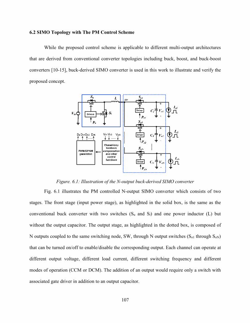
107
6.2 SIMO Topology with The PM Control Scheme
While the proposed control scheme is applicable to different multi-output architectures
that are derived from conventional converter topologies including buck, boost, and buck-boost
converters [10-15], buck-derived SIMO converter is used in this work to illustrate and verify the
proposed concept.
Figure. 6.1: Illustration of the N-output buck-derived SIMO converter
Fig. 6.1 illustrates the PM controlled N-output SIMO converter which consists of two
stages. The front stage (input power stage), as highlighted in the solid box, is the same as the
conventional buck converter with two switches (Su and Sl) and one power inductor (L) but
without the output capacitor. The output stage, as highlighted in the dotted box, is composed of
N outputs coupled to the same switching node, SW, through N output switches (So1 through SoN)
that can be turned on/off to enable/disable the corresponding output. Each channel can operate at
different output voltage, different load current, different switching frequency and different
modes of operation (CCM or DCM). The addition of an output would require only a switch with
associated gate driver in addition to an output capacitor.
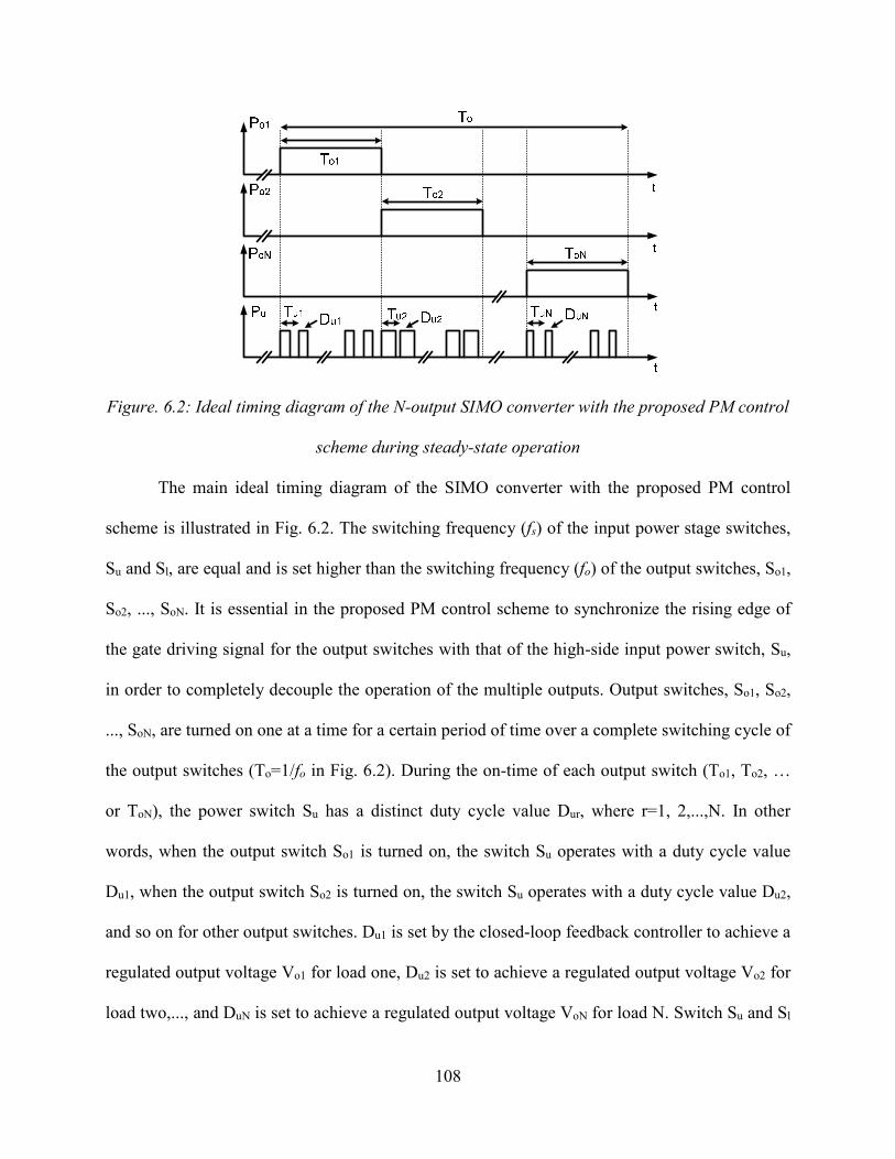
108
Figure. 6.2: Ideal timing diagram of the N-output SIMO converter with the proposed PM control
scheme during steady-state operation
The main ideal timing diagram of the SIMO converter with the proposed PM control
scheme is illustrated in Fig. 6.2. The switching frequency (fs) of the input power stage switches,
Su and Sl, are equal and is set higher than the switching frequency (fo) of the output switches, So1,
So2, ..., SoN. It is essential in the proposed PM control scheme to synchronize the rising edge of
the gate driving signal for the output switches with that of the high-side input power switch, Su,
in order to completely decouple the operation of the multiple outputs. Output switches, So1, So2,
..., SoN, are turned on one at a time for a certain period of time over a complete switching cycle of
the output switches (To=1/fo in Fig. 6.2). During the on-time of each output switch (To1, To2, …
or ToN), the power switch Su has a distinct duty cycle value Dur, where r=1, 2,...,N. In other
words, when the output switch So1 is turned on, the switch Su operates with a duty cycle value
Du1, when the output switch So2 is turned on, the switch Su operates with a duty cycle value Du2,
and so on for other output switches. Du1 is set by the closed-loop feedback controller to achieve a
regulated output voltage Vo1 for load one, Du2 is set to achieve a regulated output voltage Vo2 for
load two,..., and DuN is set to achieve a regulated output voltage VoN for load N. Switch Su and Sl
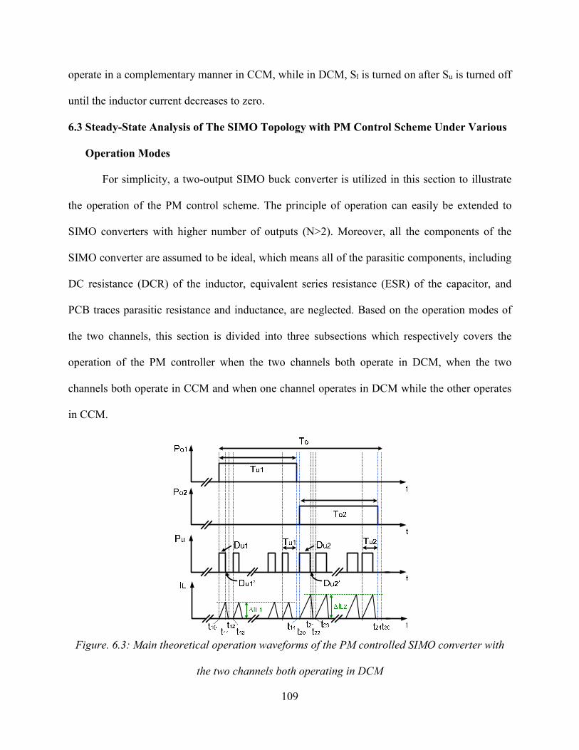
109
operate in a complementary manner in CCM, while in DCM, Sl is turned on after Su is turned off
until the inductor current decreases to zero.
6.3 Steady-State Analysis of The SIMO Topology with PM Control Scheme Under Various
Operation Modes
For simplicity, a two-output SIMO buck converter is utilized in this section to illustrate
the operation of the PM control scheme. The principle of operation can easily be extended to
SIMO converters with higher number of outputs (N>2). Moreover, all the components of the
SIMO converter are assumed to be ideal, which means all of the parasitic components, including
DC resistance (DCR) of the inductor, equivalent series resistance (ESR) of the capacitor, and
PCB traces parasitic resistance and inductance, are neglected. Based on the operation modes of
the two channels, this section is divided into three subsections which respectively covers the
operation of the PM controller when the two channels both operate in DCM, when the two
channels both operate in CCM and when one channel operates in DCM while the other operates
in CCM.
Figure. 6.3: Main theoretical operation waveforms of the PM controlled SIMO converter with
the two channels both operating in DCM
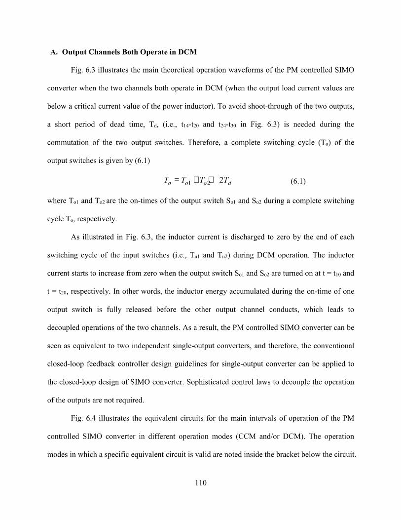
110
A. Output Channels Both Operate in DCM
Fig. 6.3 illustrates the main theoretical operation waveforms of the PM controlled SIMO
converter when the two channels both operate in DCM (when the output load current values are
below a critical current value of the power inductor). To avoid shoot-through of the two outputs,
a short period of dead time, Td, (i.e., t14-t20 and t24-t30 in Fig. 6.3) is needed during the
commutation of the two output switches. Therefore, a complete switching cycle (To) of the
output switches is given by (6.1)
1 2 2o o o dT T T T= + + (6.1)
where To1 and To2 are the on-times of the output switch So1 and So2 during a complete switching
cycle To, respectively.
As illustrated in Fig. 6.3, the inductor current is discharged to zero by the end of each
switching cycle of the input switches (i.e., Tu1 and Tu2) during DCM operation. The inductor
current starts to increase from zero when the output switch So1 and So2 are turned on at t = t10 and
t = t20, respectively. In other words, the inductor energy accumulated during the on-time of one
output switch is fully released before the other output channel conducts, which leads to
decoupled operations of the two channels. As a result, the PM controlled SIMO converter can be
seen as equivalent to two independent single-output converters, and therefore, the conventional
closed-loop feedback controller design guidelines for single-output converter can be applied to
the closed-loop design of SIMO converter. Sophisticated control laws to decouple the operation
of the outputs are not required.
Fig. 6.4 illustrates the equivalent circuits for the main intervals of operation of the PM
controlled SIMO converter in different operation modes (CCM and/or DCM). The operation
modes in which a specific equivalent circuit is valid are noted inside the bracket below the circuit.
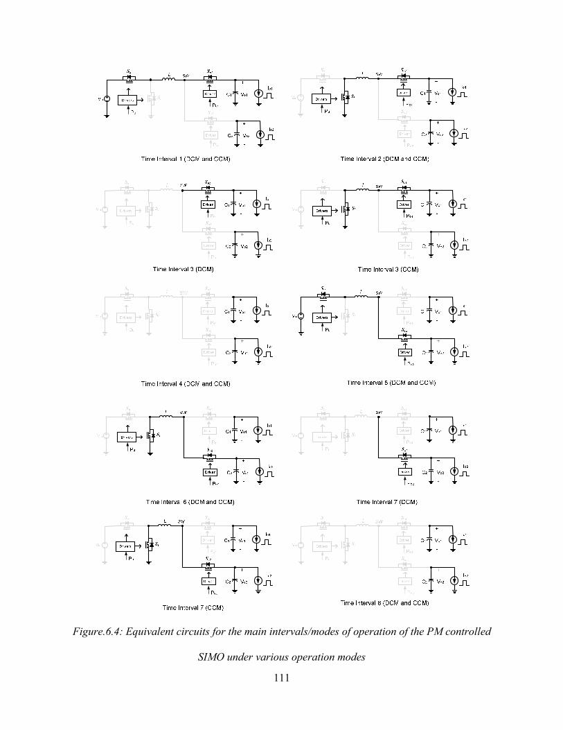
111
Figure.6.4: Equivalent circuits for the main intervals/modes of operation of the PM controlled
SIMO under various operation modes

112
The description for each DCM interval of operation during a complete switching cycle
(To) of the output switches are summarized as follows:
Time Interval 1 (t10~t11): during this time interval, the output switch So1 is turned on while
the output switch So2 is turned off. Meanwhile, switch Su is turned on while Sl is turned off. The
input voltage source charges the inductor and causes the inductor current to increase. The
relationship between the input voltage Vin, output voltage Vo1, the change in the inductor current
∆IL1, and the charging time is given by (6.2). In the meantime, the output capacitor Co2 supplies
energy to the load two.
11
11 10
in oL V VI
t t L
−∆ =− (6.2)
Time Interval 2 (t11~t12): during this time interval, the output switch So1 continues to be
turned on while the output switch So2 continues to be turned off. Meanwhile, switch Su is turned
off while Sl is turned on. The inductor is discharged to zero while delivering energy to the load
one. The relationship between the output voltage Vo1, the change in the inductor current ∆IL1,
and the discharging time is given by (6.3). In the meantime, the output capacitor Co2 still supplies
energy to the load two.
11
12 11
oL VI
t t L
∆ =− (6.3)
Time Interval 3 (t12~t13): during this time interval, the output switch So1 continues to be
turned on while the output switch So2 continues to be turned off. Meanwhile, both switch Su and
Sl are turned off. The inductor current value remains at zero. The output capacitor Co1 supplies
energy to the load one while the output capacitor Co2 supplies energy to the load two.
Applying the voltage-second balance theory to the inductor and capacitor charge balance
theory to the output capacitor one yields (6.4) and (6.5), respectively.
113
1 1
'1 1
o u
in u u
V D
V D D=
+ (6.4)
'1 1 1 1 1
1
( )( )
2
u u u in o u uL
D D D V V D TI
L
+ −= (6.5)
where Du1' is equal to the time the inductor current takes to discharge to zero divided by the
switching cycle of switch Su; IL1 is the average inductor current during on-time of the output
switch So1, and it is also given by (6.6) because the inductor current is effectively zero for
channel one when the output switch So1 is turned off while So2 is turned on.
1 1
11 1 1
o o o oL
o o o
I T V TI
T R T= = (6.6)
where Ro1 is the load resistance for output one and Io1 is the load current for output one. Based on
(6.4), (6.5) and (6.6), the DC voltage gain for the channel one can be derived as given by
1
21 1
2
1 1 4
o
in u
V
V K D=
+ + (6.7)
where K1=2LTo/(Ro1Tu1To1), and Du1 is the duty cycle value of switch Su when the output switch
So1 is turned on.
Time Interval 4 (t14~t20): during this short dead-time period, the input switches Su and Sl
are both turned off and the output switches So1 and So2 are turned off as well. Unlike the
synchronous rectifier in the front power stage of the SIMO converter, the body diodes of the two
output switches So1 and So2 cannot conduct during this dead-time period to provide a path for the
inductor current to flow. Therefore, it is critical to ensure that the inductor current returns to zero
before the dead-time period starts in order to avoid a voltage spike on the output switching node
SW. DCM operation certainly meets this requirement as the inductor current returns to zero by
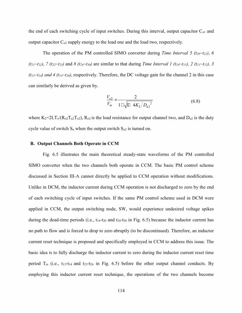
114
the end of each switching cycle of input switches. During this interval, output capacitor Co1 and
output capacitor Co2 supply energy to the load one and the load two, respectively.
The operation of the PM controlled SIMO converter during Time Interval 5 (t20~t21), 6
(t21~t22), 7 (t22~t23) and 8 (t24~t30) are similar to that during Time Interval 1 (t10~t11), 2 (t11~t12), 3
(t13~t14) and 4 (t14~t20), respectively. Therefore, the DC voltage gain for the channel 2 in this case
can similarly be derived as given by.
2
22 2
2
1 1 4
o
in u
V
V K D=
+ + (6.8)
where K2=2LTo/(Ro2Tu2To2), Ro2 is the load resistance for output channel two, and Du2 is the duty
cycle value of switch Su when the output switch So2 is turned on.
B. Output Channels Both Operate in CCM
Fig. 6.5 illustrates the main theoretical steady-state waveforms of the PM controlled
SIMO converter when the two channels both operate in CCM. The basic PM control scheme
discussed in Section III-A cannot directly be applied to CCM operation without modifications.
Unlike in DCM, the inductor current during CCM operation is not discharged to zero by the end
of each switching cycle of input switches. If the same PM control scheme used in DCM were
applied in CCM, the output switching node, SW, would experience undesired voltage spikes
during the dead-time periods (i.e., t14-t20 and t24-t30 in Fig. 6.5) because the inductor current has
no path to flow and is forced to drop to zero abruptly (to be discontinued). Therefore, an inductor
current reset technique is proposed and specifically employed in CCM to address this issue. The
basic idea is to fully discharge the inductor current to zero during the inductor current reset time
period Trs (i.e., t13-t14 and t23-t24 in Fig. 6.5) before the other output channel conducts. By
employing this inductor current reset technique, the operations of the two channels become
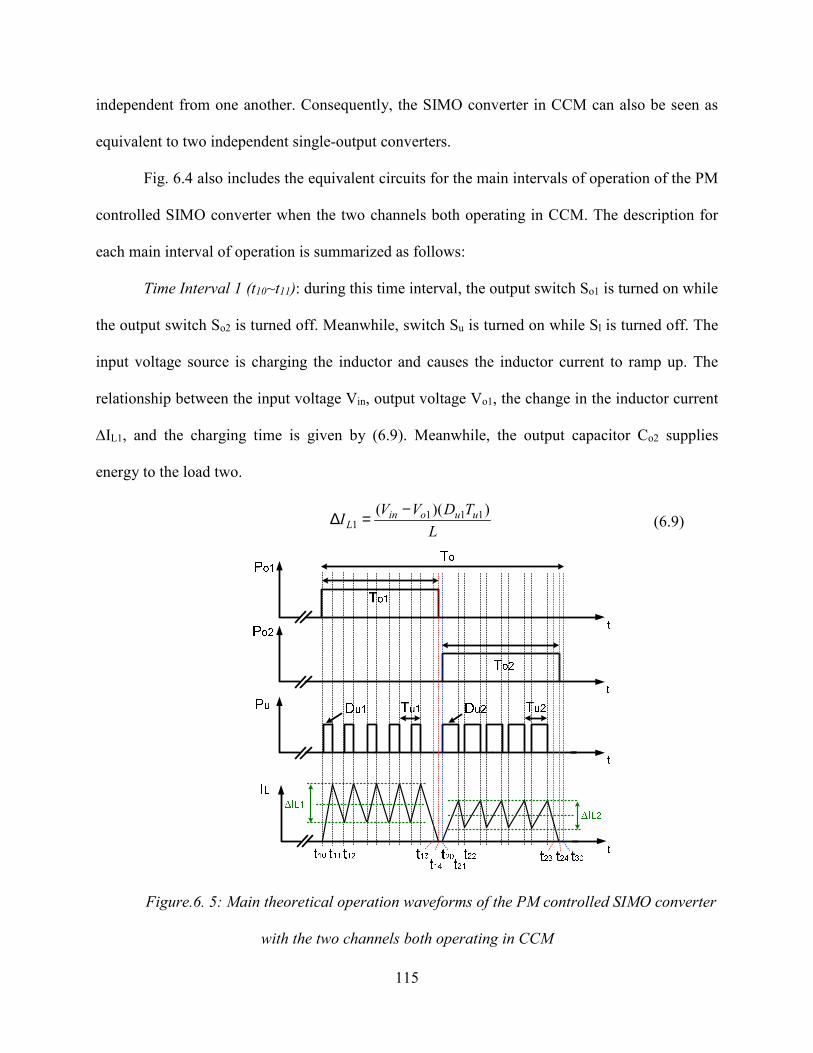
115
independent from one another. Consequently, the SIMO converter in CCM can also be seen as
equivalent to two independent single-output converters.
Fig. 6.4 also includes the equivalent circuits for the main intervals of operation of the PM
controlled SIMO converter when the two channels both operating in CCM. The description for
each main interval of operation is summarized as follows:
Time Interval 1 (t10~t11): during this time interval, the output switch So1 is turned on while
the output switch So2 is turned off. Meanwhile, switch Su is turned on while Sl is turned off. The
input voltage source is charging the inductor and causes the inductor current to ramp up. The
relationship between the input voltage Vin, output voltage Vo1, the change in the inductor current
∆IL1, and the charging time is given by (6.9). Meanwhile, the output capacitor Co2 supplies
energy to the load two.
1 1 1
1
( )( )in o u uL
V V D TI
L
−∆ = (6.9)
Figure.6. 5: Main theoretical operation waveforms of the PM controlled SIMO converter
with the two channels both operating in CCM
116
Time Interval 2 (t11~t12): In this mode, the output switch So1 continues to be turned on and
the output switch So2 continues to be turned off. Meanwhile, switch Su is turned off while Sl is
turned on. The inductor is discharged while delivering energy to the load one. The relationship
between the output voltage Vo1, the change in the inductor current ∆IL1, and the discharge time is
given by (6.10). The output capacitor Co2 continues to supply energy to the load two. Based on
(6.9) and (6.10), the DC voltage gain for the channel one is given by (6.11)
1 1 1
1
(1 )o u uL
V D TI
L
−∆ = (6.10)
1
1o
uin
VD
V= (6.11)
Time Interval 3 (t13~t14): during this time interval, the inductor current is being reset. The
output switch So1 continues to be turned on while the output switch So2 continues to be turned
off. Switch Su continues to be turned off and Sl continues to be turned on. Output capacitor Co2
continues to supply energy to the load two. The inductor continues to discharge with a slew rate
of Vo1/L.
The optimal inductor current reset time for channel one Trs_ch1_opt occurs when the
inductor current reaches zero right before the dead-time period starts at t=t14, as shown in Fig.
6.5. Therefore, Trs_ch1_opt is given by
1 1
_ 1_1
( 2)L Lrs ch opt
o
I I LT
V
− ∆= (6.12)
Substituting (6.6) and (6.10) into (6.12) yields
1 1 1 1
1 1_ 1_
1
(1 )( )
2o o o u u
o ors ch opt
o
V T V D TL
R T LT
V
−−= (6.13)
Generalizing (6.13) for any other channel yields
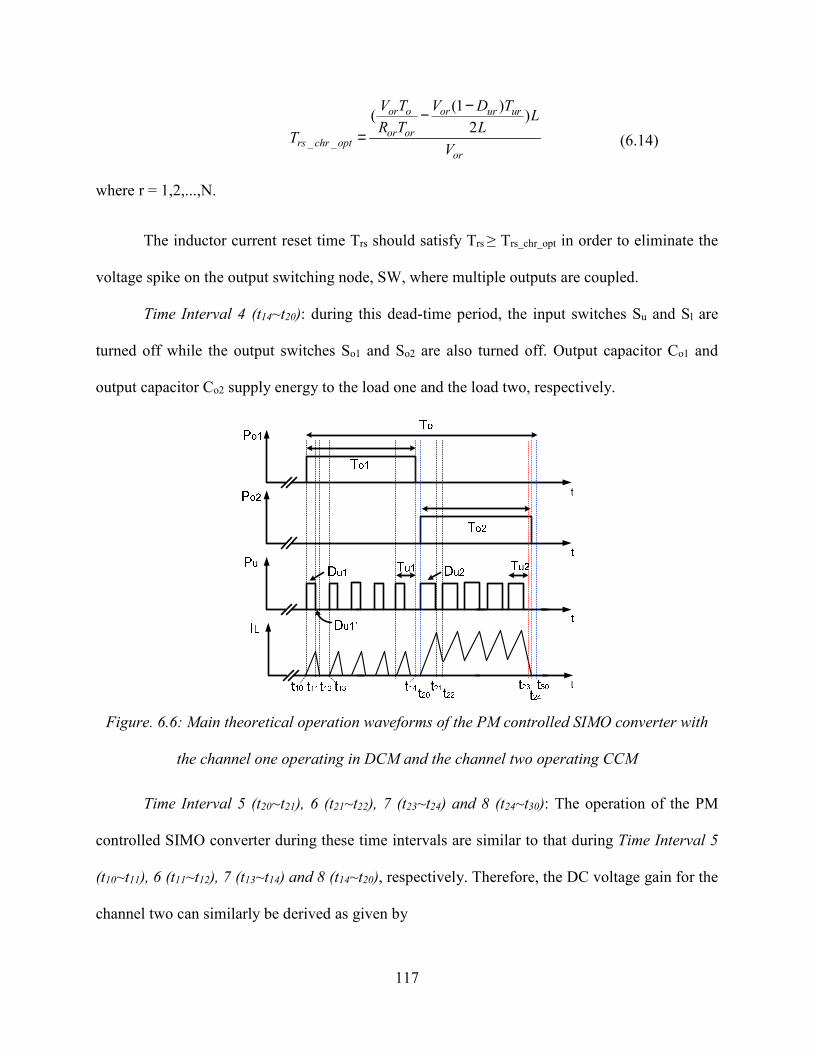
117
_ _
(1 )( )
2or o or ur ur
or orrs chr opt
or
V T V D TL
R T LT
V
−−= (6.14)
where r = 1,2,...,N.
The inductor current reset time Trs should satisfy Trs ≥ Trs_chr_opt in order to eliminate the
voltage spike on the output switching node, SW, where multiple outputs are coupled.
Time Interval 4 (t14~t20): during this dead-time period, the input switches Su and Sl are
turned off while the output switches So1 and So2 are also turned off. Output capacitor Co1 and
output capacitor Co2 supply energy to the load one and the load two, respectively.
Figure. 6.6: Main theoretical operation waveforms of the PM controlled SIMO converter with
the channel one operating in DCM and the channel two operating CCM
Time Interval 5 (t20~t21), 6 (t21~t22), 7 (t23~t24) and 8 (t24~t30): The operation of the PM
controlled SIMO converter during these time intervals are similar to that during Time Interval 5
(t10~t11), 6 (t11~t12), 7 (t13~t14) and 8 (t14~t20), respectively. Therefore, the DC voltage gain for the
channel two can similarly be derived as given by
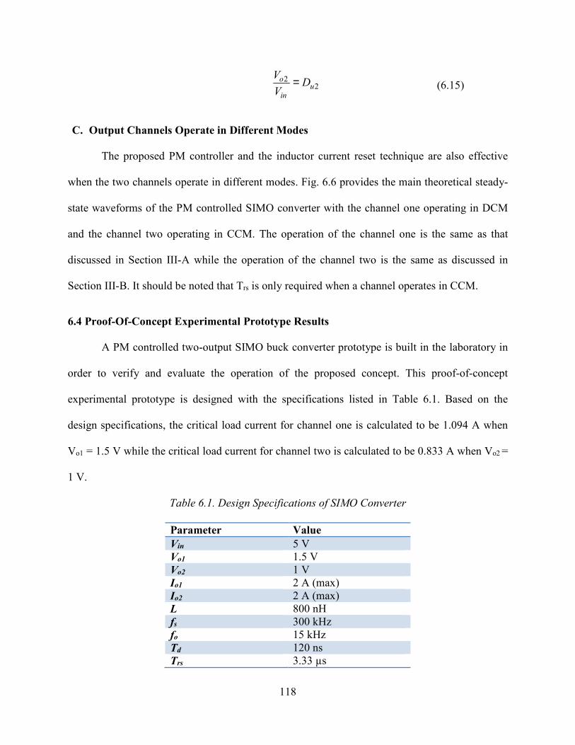
118
2
2o
uin
VD
V= (6.15)
C. Output Channels Operate in Different Modes
The proposed PM controller and the inductor current reset technique are also effective
when the two channels operate in different modes. Fig. 6.6 provides the main theoretical steady-
state waveforms of the PM controlled SIMO converter with the channel one operating in DCM
and the channel two operating in CCM. The operation of the channel one is the same as that
discussed in Section III-A while the operation of the channel two is the same as discussed in
Section III-B. It should be noted that Trs is only required when a channel operates in CCM.
6.4 Proof-Of-Concept Experimental Prototype Results
A PM controlled two-output SIMO buck converter prototype is built in the laboratory in
order to verify and evaluate the operation of the proposed concept. This proof-of-concept
experimental prototype is designed with the specifications listed in Table 6.1. Based on the
design specifications, the critical load current for channel one is calculated to be 1.094 A when
Vo1 = 1.5 V while the critical load current for channel two is calculated to be 0.833 A when Vo2 =
1 V.
Table 6.1. Design Specifications of SIMO Converter
Parameter Value
Vin 5 V
Vo1 1.5 V
Vo2 1 V
Io1 2 A (max)
Io2 2 A (max)
L 800 nH
fs 300 kHz
fo 15 kHz
Td 120 ns
Trs 3.33 µs
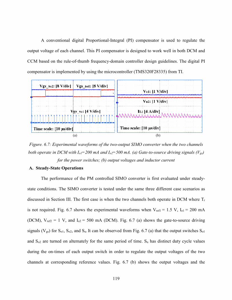
119
A conventional digital Proportional-Integral (PI) compensator is used to regulate the
output voltage of each channel. This PI compensator is designed to work well in both DCM and
CCM based on the rule-of-thumb frequency-domain controller design guidelines. The digital PI
compensator is implemented by using the microcontroller (TMS320F28335) from TI.
(a) (b)
Figure. 6.7: Experimental waveforms of the two-output SIMO converter when the two channels
both operate in DCM with Io1=200 mA and Io2=500 mA. (a) Gate-to-source driving signals (Vgs)
for the power switches; (b) output voltages and inductor current
A. Steady-State Operations
The performance of the PM controlled SIMO converter is first evaluated under steady-
state conditions. The SIMO converter is tested under the same three different case scenarios as
discussed in Section III. The first case is when the two channels both operate in DCM where Tr
is not required. Fig. 6.7 shows the experimental waveforms when Vref1 = 1.5 V, Io1 = 200 mA
(DCM), Vref2 = 1 V, and Io2 = 500 mA (DCM). Fig. 6.7 (a) shows the gate-to-source driving
signals (Vgs) for So1, So2, and Su. It can be observed from Fig. 6.7 (a) that the output switches So1
and So2 are turned on alternately for the same period of time. Su has distinct duty cycle values
during the on-times of each output switch in order to regulate the output voltages of the two
channels at corresponding reference values. Fig. 6.7 (b) shows the output voltages and the
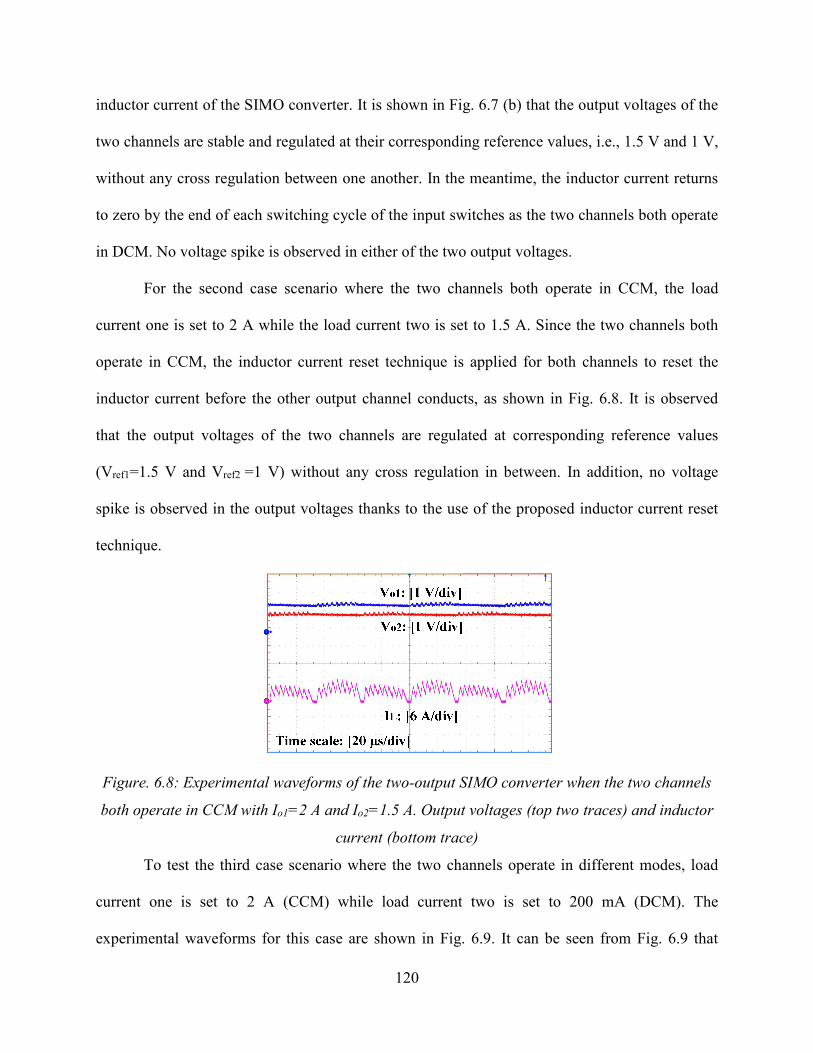
120
inductor current of the SIMO converter. It is shown in Fig. 6.7 (b) that the output voltages of the
two channels are stable and regulated at their corresponding reference values, i.e., 1.5 V and 1 V,
without any cross regulation between one another. In the meantime, the inductor current returns
to zero by the end of each switching cycle of the input switches as the two channels both operate
in DCM. No voltage spike is observed in either of the two output voltages.
For the second case scenario where the two channels both operate in CCM, the load
current one is set to 2 A while the load current two is set to 1.5 A. Since the two channels both
operate in CCM, the inductor current reset technique is applied for both channels to reset the
inductor current before the other output channel conducts, as shown in Fig. 6.8. It is observed
that the output voltages of the two channels are regulated at corresponding reference values
(Vref1=1.5 V and Vref2 =1 V) without any cross regulation in between. In addition, no voltage
spike is observed in the output voltages thanks to the use of the proposed inductor current reset
technique.
Figure. 6.8: Experimental waveforms of the two-output SIMO converter when the two channels
both operate in CCM with Io1=2 A and Io2=1.5 A. Output voltages (top two traces) and inductor
current (bottom trace)
To test the third case scenario where the two channels operate in different modes, load
current one is set to 2 A (CCM) while load current two is set to 200 mA (DCM). The
experimental waveforms for this case are shown in Fig. 6.9. It can be seen from Fig. 6.9 that
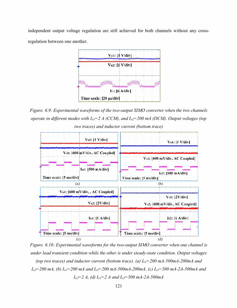
121
independent output voltage regulation are still achieved for both channels without any cross-
regulation between one another.
Figure. 6.9: Experimental waveforms of the two-output SIMO converter when the two channels
operate in different modes with Io1=2 A (CCM), and Io2=200 mA (DCM). Output voltages (top
two traces) and inductor current (bottom trace)
(a) (b)
(c) (d)
Figure. 6.10: Experimental waveforms for the two-output SIMO converter when one channel is
under load transient condition while the other is under steady-state condition. Output voltages
(top two traces) and inductor current (bottom trace). (a) Io1=200 mA-500mA-200mA and
Io2=200 mA, (b) Io1=200 mA and Io2=200 mA-500mA-200mA, (c) Io1=500 mA-2A-500mA and
Io2=2 A, (d) Io1=2 A and Io2=500 mA-2A-500mA
Time scale: [5 ms/div]
Vo1: [600 mV/div, , AC Coupled]
Vo2: [2V/div]
Io1: [1 A/div]
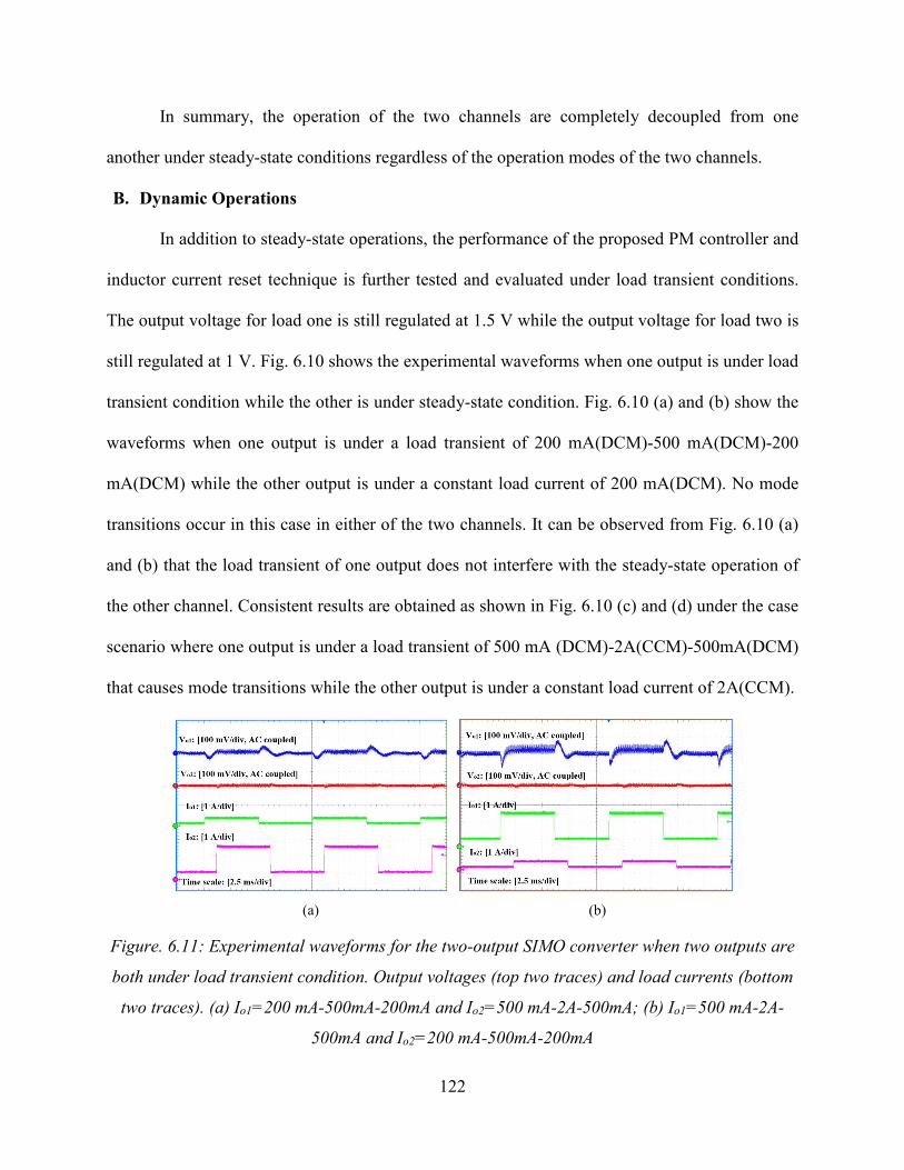
122
In summary, the operation of the two channels are completely decoupled from one
another under steady-state conditions regardless of the operation modes of the two channels.
B. Dynamic Operations
In addition to steady-state operations, the performance of the proposed PM controller and
inductor current reset technique is further tested and evaluated under load transient conditions.
The output voltage for load one is still regulated at 1.5 V while the output voltage for load two is
still regulated at 1 V. Fig. 6.10 shows the experimental waveforms when one output is under load
transient condition while the other is under steady-state condition. Fig. 6.10 (a) and (b) show the
waveforms when one output is under a load transient of 200 mA(DCM)-500 mA(DCM)-200
mA(DCM) while the other output is under a constant load current of 200 mA(DCM). No mode
transitions occur in this case in either of the two channels. It can be observed from Fig. 6.10 (a)
and (b) that the load transient of one output does not interfere with the steady-state operation of
the other channel. Consistent results are obtained as shown in Fig. 6.10 (c) and (d) under the case
scenario where one output is under a load transient of 500 mA (DCM)-2A(CCM)-500mA(DCM)
that causes mode transitions while the other output is under a constant load current of 2A(CCM).
(a) (b)
Figure. 6.11: Experimental waveforms for the two-output SIMO converter when two outputs are
both under load transient condition. Output voltages (top two traces) and load currents (bottom
two traces). (a) Io1=200 mA-500mA-200mA and Io2=500 mA-2A-500mA; (b) Io1=500 mA-2A-
500mA and Io2=200 mA-500mA-200mA
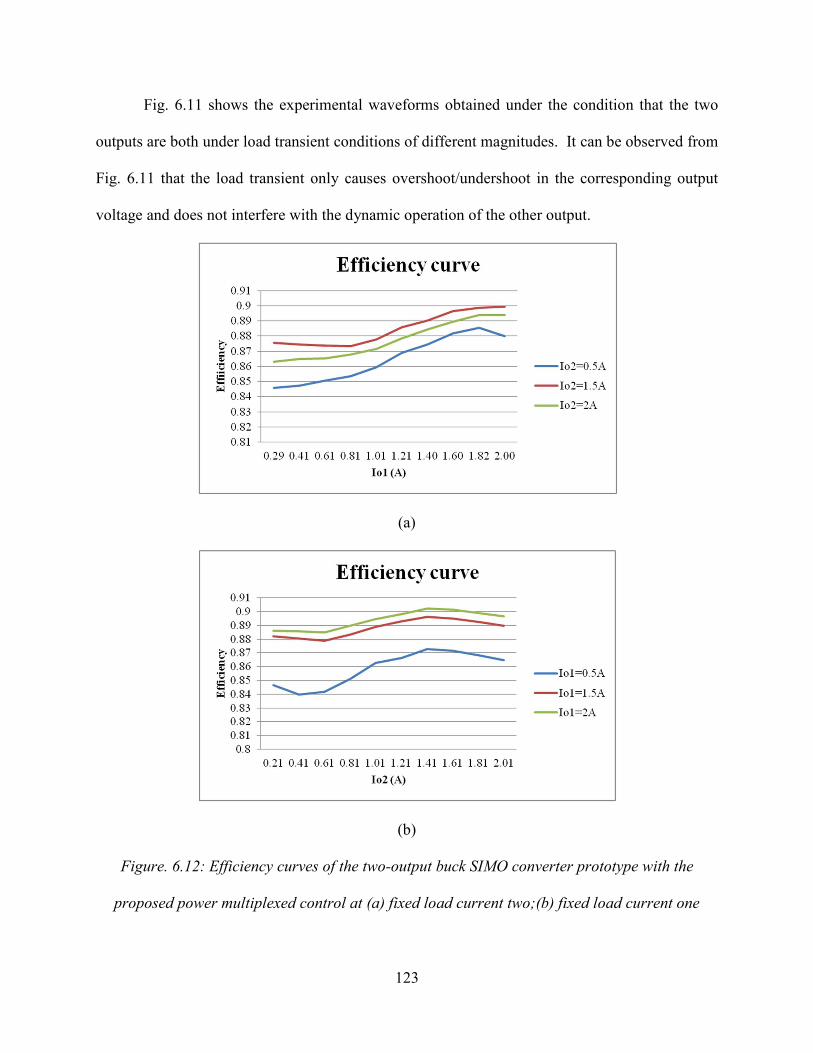
123
Fig. 6.11 shows the experimental waveforms obtained under the condition that the two
outputs are both under load transient conditions of different magnitudes. It can be observed from
Fig. 6.11 that the load transient only causes overshoot/undershoot in the corresponding output
voltage and does not interfere with the dynamic operation of the other output.
(a)
(b)
Figure. 6.12: Efficiency curves of the two-output buck SIMO converter prototype with the
proposed power multiplexed control at (a) fixed load current two;(b) fixed load current one
124
Fig. 6.12 shows the efficiency curves of the two-output buck SIMO converter prototype
with the proposed PM controller under different operating conditions. It can be seen that the
efficiency of the converter peaks at 90.2% when the load current one is 2A and load current two
is 1.41A. Also, it can be noticed that the efficiency curves exhibit consistent trends at different
load currents.
C. Three-Output SIMO Experimental Results
Sample experimental results obtained from a preliminary three-output SIMO converter
prototype are shown in this section to further show the effectiveness of the proposed PM
controller. Fig. 6.13 through Fig.6.15 show the steady state waveforms for the prototype with
three outputs. Note that the input and output switches’ frequencies are set at 300kHz and 30kHz,
respectively. In other words, each output switch period contains 10 input switch periods. The
duty cycle values for the three output switches are 40%, 30%, 30%. The reference output voltage
and load current information for each channel are summarized below:
Vref1 = 1.5V, Io1 = 0.5A Vref2 = 1.8V, Io2 = 0.7A Vref3 = 1.5V, Io3 = 0.6A
It can be observed from Fig. 6.15 that the output voltage of each channel is regulated at
its reference value without any cross regulation between the channels.
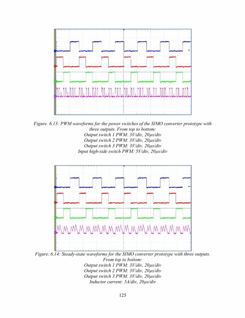
125
Figure. 6.13: PWM waveforms for the power switches of the SIMO converter prototype with
three outputs. From top to bottom:
Output switch 1 PWM: 3V/div, 20µs/div
Output switch 2 PWM: 3V/div, 20µs/div
Output switch 3 PWM: 3V/div, 20µs/div
Input high-side switch PWM: 5V/div, 20µs/div
Figure. 6.14: Steady-state waveforms for the SIMO converter prototype with three outputs.
From top to bottom:
Output switch 1 PWM: 3V/div, 20µs/div
Output switch 2 PWM: 3V/div, 20µs/div
Output switch 3 PWM: 3V/div, 20µs/div
Inductor current: 5A/div, 20µs/div
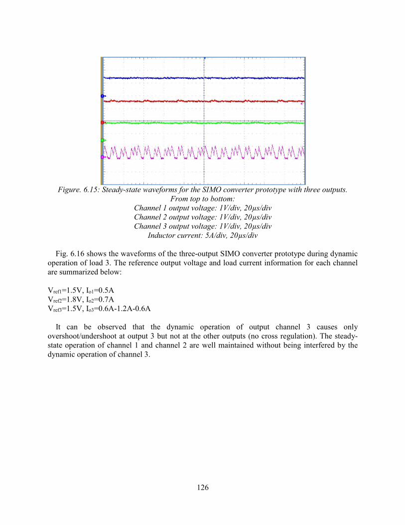
126
Figure. 6.15: Steady-state waveforms for the SIMO converter prototype with three outputs.
From top to bottom:
Channel 1 output voltage: 1V/div, 20µs/div
Channel 2 output voltage: 1V/div, 20µs/div
Channel 3 output voltage: 1V/div, 20µs/div
Inductor current: 5A/div, 20µs/div
Fig. 6.16 shows the waveforms of the three-output SIMO converter prototype during dynamic operation of load 3. The reference output voltage and load current information for each channel are summarized below: Vref1=1.5V, Io1=0.5A Vref2=1.8V, Io2=0.7A Vref3=1.5V, Io3=0.6A-1.2A-0.6A It can be observed that the dynamic operation of output channel 3 causes only overshoot/undershoot at output 3 but not at the other outputs (no cross regulation). The steady-state operation of channel 1 and channel 2 are well maintained without being interfered by the dynamic operation of channel 3.
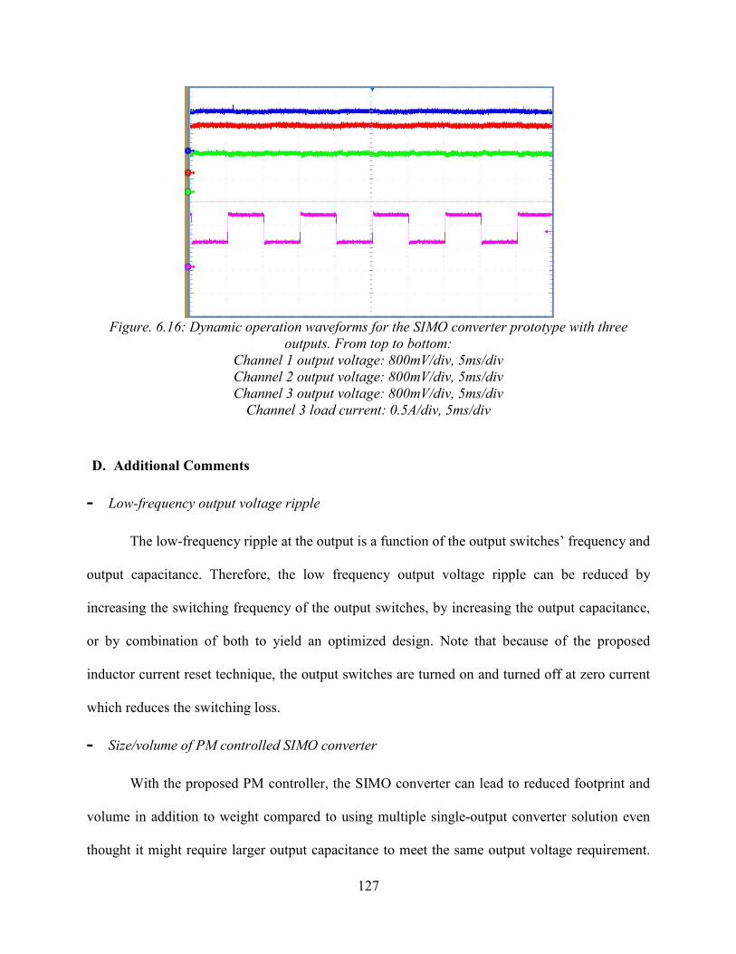
127
Figure. 6.16: Dynamic operation waveforms for the SIMO converter prototype with three
outputs. From top to bottom:
Channel 1 output voltage: 800mV/div, 5ms/div
Channel 2 output voltage: 800mV/div, 5ms/div
Channel 3 output voltage: 800mV/div, 5ms/div
Channel 3 load current: 0.5A/div, 5ms/div
D. Additional Comments
- Low-frequency output voltage ripple
The low-frequency ripple at the output is a function of the output switches’ frequency and
output capacitance. Therefore, the low frequency output voltage ripple can be reduced by
increasing the switching frequency of the output switches, by increasing the output capacitance,
or by combination of both to yield an optimized design. Note that because of the proposed
inductor current reset technique, the output switches are turned on and turned off at zero current
which reduces the switching loss.
- Size/volume of PM controlled SIMO converter
With the proposed PM controller, the SIMO converter can lead to reduced footprint and
volume in addition to weight compared to using multiple single-output converter solution even
thought it might require larger output capacitance to meet the same output voltage requirement.
128
This is because the footprint and volume reduction resulted from the power inductors, switches,
drivers, and their corresponding traces/interconnections surpasses the added foot print and
volume of the output capacitors. Note that the technological advances has resulted in increasing
the capacitors’ density at a faster rate than increasing the power inductors’ density.
It can be shown that for an example SIMO converter design with three outputs, more than
14% net reduction in component’s footprint and more than 20% net reduction in component’s
volume can be achieved when using commercially available components. For this SIMO
converter with the proposed controller, it require one power inductor instead of three power
inductors, five MOSFETs instead of six MOSFETs, and five gate drivers instead of six gate
drivers, while requiring some additional output capacitors to meet the same ripple requirements
when the SIMO converter’s output switches operate at lower switching frequency than the
switching frequency of three individual single output converters.
6.5 Summary
This chapter presents a power-multiplexed control scheme for a SIMO power switching
converter. The PM control scheme results in eliminating the cross regulation between the
multiple outputs while maintaining voltage regulation for each output during steady-state and
dynamic operations. To eliminate the voltage spike on the output switching node during CCM
operation, a simple inductor current reset technique is proposed. The PM controller can be
implemented with a low-cost microcontroller or analog circuitries due to its simplicity. A two-
output buck derived SIMO converter is utilized as an example in this work to illustrate and verify
the operation of the proposed controller. Experimental results verify the effectiveness and
performance of the proposed PM control scheme under different case scenarios.
129
CHAPTER 7
CONCLUSIONS AND FUTURE WORK
7.1 Summary of Conclusions
Batteries have been widely used in many applications including portable electronics,
EVs/HEVs, and distributed smart power grids. In addition to the advances of the battery
technologies, the BMS plays a critical role in ensuring the efficient, reliable and safe operation of
the battery pack and the system it powers. Among the functions of BMS, part of this dissertation
work focus on addressing the issues related to online battery impedance
measurement/monitoring and cell balancing for discharging and charging operation.
In addition to the BMS issues, this dissertation also addresses the common cross
regulation issue related to the SIMO converters which have gain popularity in battery-powered
applications due to the advantages including reduced number of components, size and cost as
compared to multiple-converter solution. The cross regulation issue has been a key obstacle
preventing the widespread adoption of the SIMO converter in broad range of applications.
To address the aforementioned issues, this dissertation proposes several advanced control
and power management schemes utilizing the flexibility of digital controller. The contribution of
this research work include the research and development of the following concepts: (1) Online
battery impedance measurement method; (2) Energy sharing controller for cell balancing in
battery discharge mode; (3) Battery charging controller with energy sharing for cell balancing
during charging operation; (5) Small-signal modeling and analysis of the energy sharing
controlled distributed battery system; (6) Power-multiplexed controller addressing the cross
130
regulation issue of the SIMO converters during both steady-state and dynamic operation
regardless of the operating mode of each output channel, i.e., CCM or DCM. All of the proposed
control and power management schemes have been validated and evaluated with proof-of-
concept experimental prototype results.
7.1.1. Online Impedance Measurement Method
This dissertation first proposes an online impedance measurement method for
electrochemical batteries. The battery impedance measurement is realized via the control and
perturbation of the DC-DC power converter which interfaces the battery with the load. With the
proposed method, the signal generation circuits/devices required by the existing impedance
measurement methods are eliminated, which leads to reduced cost, design complexities and size
of the overall system. This method can be performed either continuously or periodically without
interrupting the normal operation of the battery system and power converter. The proposed
method is well suited for real-time battery impedance monitoring.
In addition, a practical online SOC estimation method for lithium-ion batteries is
provided in this dissertation based on the obtained impedance data. With the proposed method,
there is no need to put the battery in rest/relaxation mode for a long period of time in order to
reach electrochemical equilibrium prior to the OCV measurement. Experimental results have
validated the effectiveness of the proposed online impedance measurement method and its
utilization in the online SOC estimation.
7.1.2. Energy Sharing Controller for Cell Balancing in Battery Discharge Mode
An energy sharing controller is proposed in this dissertation based on a distributed battery
system architecture. The DC-DC power converters with the proposed energy sharing controller
are utilized to achieve SOC balancing between the battery cells while providing DC bus voltage
131
regulation to the rest of the system or load. As a result, there is no need for two independent
converter systems for cell SOC balancing. This results in reduced design complexity of the
battery energy storage system.
The proposed energy sharing controller addresses the battery cells' SOC imbalance issue
from the root by adjusting the discharge rate of each cell while maintaining the total regulated
DC bus voltage. The energy transfer between the battery cells which is usually required in the
existing cell balancing solutions is no longer needed, thus eliminating the power losses caused by
the energy transfer process.
The proof-of-concept experimental prototype results have validated the performance of
the proposed energy sharing controller during discharging operation. The developed architecture
and energy sharing controller is an attractive candidate for many battery energy storage
applications including EVs/PHEVs (which utilize power distribution scheme that has a DC-DC
power converter), DC microgrids, aerospace battery systems, laptop computers battery packs,
and other portable devices with multi-cell battery energy storage.
7.1.3. Battery Charging Controller with Energy Sharing
The energy sharing controller proposed in the Chapter 3 is upgraded by integrating a
battery charging control algorithm with the energy sharing concept in order to address the cell
balancing issue during battery charging operation. The upgraded battery charging controller also
addresses the battery cells' charge imbalance issue from the root by adjusting the charge rate of
each battery cell while maintaining the average cell current to be regulated at a given level. The
energy transfer between the battery cells is eliminated, thus leading to increased efficiency of the
battery system. The experimental prototype results have validated the cell balancing performance
of the upgraded battery charging controller with energy sharing during charging operation.
132
7.1.4. Small-Signal Modeling and Energy Sharing Controller Design
State-space averaging small-signal modeling and analysis is performed in Chapter 5 in
order to gain deeper insights into the dynamics of the energy sharing controlled distributed
battery system during both discharging and charging operation. Based on the derived small-
signal models and associated transfer functions, the control loops are compensated for different
operation mode, including discharge mode, constant current charging mode and constant voltage
charging mode, based on the rule-of-thumb frequency-domain design guidelines and criteria. The
simulation and experimental results obtained from a two-cell distributed battery system
prototype have validated the derived small signal models and designed closed-loop
compensators.
7.1.5. Power-Multiplexed Controller for SIMO Converters
In addition to addressing several BMS issues, this dissertation also proposes a power-
multiplexed control scheme to address the cross regulation issue of SIMO switching converters
which are increasingly used in portable applications where a battery powers multiple electronic
loads. The PM control scheme completely decouples the operation of each output by
multiplexing the conduction of each output switch. To eliminate the voltage spike on the output
switching node during CCM operation, a simple inductor current reset technique is proposed.
The PM controller can be implemented with a low-cost microcontroller or analog circuitries
thanks to its simplicity. A two-output buck derived SIMO converter is utilized as an example in
this work to illustrate and verify the operation of the proposed controller. Proof-of-concept
experimental results are presented to verify the operation of the proposed PM control scheme
under different case scenarios.
133
7.2 Future Research Directions
The following subsections give a brief outlook on some possible future research
directions that are related to the work presented in this dissertation.
7.2.1. Accurate SOC Estimation
In Chapter 3 and 4, an energy sharing controller is proposed to achieve SOC balancing
between the battery cells in a battery pack during discharging and charging operation,
respectively. The accuracy of the SOC estimation directly impacts the performance and
reliability of the proposed energy sharing controller as it is the case in other SOC balancing
schemes. If the SOC estimation is not accurate, overdischarge or overcharge of the cells is likely
to occur. The commonly used coulomb counting method is utilized in this work for the battery
SOC estimation. As mentioned in Chapter 3 and 4, coulomb counting method has some
downsides. For instance, it does not take into account factors that may change the usable
capacity of the battery, such as temperature variation, discharge/charge rate, and aging effects,
among others. Moreover, the coulomb counting method is highly sensitive to the initial SOC
value and current measurement accuracy. The disadvantages of some other SOC estimation
methods are summarized in Section 1.2.C of Chapter 1. Therefore, a more accurate and reliable
SOC estimation method is needed in order to achieve desired cell balancing performance of the
proposed energy sharing controller. In addition to the need for an accurate and fast current sensor
(fast ADC is needed if digital control is used), the battery impedance information obtained by the
method proposed in Chapter 2 has the potential to be used for providing insights into the health
condition and capacity variation of the battery. This can lead to a more accurate SOC estimation
results.
134
7.2.2. Online Battery SOH Estimation
Another important aspect of BMS is the SOH estimation of the battery cells during online
operation for efficient power and energy management of the battery system. By modifying the
single cell impedance measurement method proposed in Chapter 2, online multi-cell impedance
measurement can be accomplished with the distributed battery system architecture used in
Chapter 3 and 4. As the impedance of the battery itself reflects the variation of many factors such
as temperature, capacity and electrochemical characteristics, the accuracy of the SOH estimation
should be improved if the impedance data is utilized along with the approachs/techniques
presented in the literature. For example, reference [30-31] reveal that the battery impedance
growth at the trough frequency of the second semi-circle on the impedance spectrum highly
correlates with the power fade, or SOH, of the battery cell. Other new techniques can also be
explored to produce a more accurate and robust SOH estimation.
7.2.3. High Power Density Integration of The Distributed Battery System
In order to be applied in real-world applications, such as EVs/HEVs, the proposed energy
sharing controlled distributed battery system architecture must be optimized in terms of power
density, efficiency, cost, EMI, and thermal performance, among others. To achieve higher power
density BPM design, other topologies can also be explored which feature lower count of
magnetic components (such as switch-capacitor based converter topologies), fewer power
switches, and reduced filter requirement, among others. Efficiency can be further improved by
using power FETs with lower gate charge, less parasitics and lower on-resistance. In addition,
the BPM efficiency is expected to be improved by using multi-layer PCB design with better
component placement and trace routing.

135
From the battery system point of view, higher power density can be achieved through
better integration of the BPMs and external functional blocks, such as thermal management and
communication, among others.
7.2.4. Adaptive Optimization of The Inductor Current Reset Time
During the CCM operation of the PM controlled SIMO converter discussed in Chapter 6,
the inductor current needs to be reset before another output channel conducts in order to prevent
the cross regulation between the outputs. In this work, the inductor current reset time is set to a
large value with sufficient margin allowing the inductor current to fully reset under all load and
input voltage conditions. However, in order to achieve optimized efficiency and output voltage
ripple, it is advantageous to dynamically optimize this inductor current reset time under different
operating conditions. This could be achieved by calculating the time it takes for the inductor
current to drop to zero under different Vin and Io conditions at the beginning of the conduction
period of a given output channel.
136
REFERENCES
CHAPTER 1
(1) A. Kuperman, U. Levy, J. Goren, A. Zafransky, and A. Savernin, " Battery Charger for Electric Vehicle Traction Battery Switch Station," IEEE Trans. Ind. Electron., vol. 60, no. 12, pp. 5391- 5399, Dec. 2013.
(2) David Velasco de la Fuente, Cesar L. Trujillo Rodriguez, and Gabriel Garcera, " Photovoltaic Power System with Battery Backup with Grid-Connection and Islanded Operation Capabilities, " IEEE Trans. Ind. Electron., vol. 60, no. 4, pp. 1571-1581, April 2013.
(3) Manuela Sechilariu, Baochao Wang, and Fabrice Locment, " Building Integrated Photovoltaic System with Energy Storage and Smart Grid Communication, " IEEE Trans. Ind. Electron., vol. 60, no. 4, pp. 1607- 1618, April 2013.
(4) Aymen Chaouachi, Rashad M., Kamel Andoulsi, and Ken Nagasaka, " Multiobjective Intelligent Energy Management for a Microgrid, " IEEE Trans. Ind. Electron., vol. 60, no. 4, pp. 1688 - 1698, April 2013.
(5) Carlos G.C.Branco, Rene P. Torrico-Bascope, Cicero M. T. Cruz, and Francisco K. de A. Lima, " Proposal of Three-Phase High-Frequency Transformer Isolation UPS Topologies for Distributed Generation Applications, " IEEE Trans. Ind. Electron., vol. 60, no. 4, pp. 1520-1531, April 2013.
(6) Roy Chaoming, Cheng-Ting Liu, and Din-Yuen Chan, " A reinforcement-Learning-Based Assisted Power Management with QoR Provisioning for Human-Electric Hybrid Bicycle," IEEE Trans. Ind. Electron., vol. 59, no. 8, pp. 3350-3359, Aug. 2012.
(7) Advanced Research Projects Agency – Energy (ARPA-E), U. S. Department of Energy, “Advanced Management and Protection of Energy Storage Devices,” DE-FOA-0000675, April 2012.
(8) iPhone 4S teardown reveals $196 cost and changes in key suppliers [online]. Available: http://venturebeat.com/2011/10/20/iphone-4s-teardown-reveals-196-cost-and-key-suppliers/.
(9) iPad Mini 4 teardown: a hard to repair mini iPad Air 2 [online]. Available: http://www.slashgear.com/ipad-mini-4-teardown-a-hard-to-repair-mini-ipad-air-2-18405432/.
(10) Retina Macbook 2015 teardown [online]. Available: https://ifixit.org/blog/7147/retina-macbook-2015-teardown/.
137
(11) Tesla Model S electric car spotted in Abu Dhabi [online]. Available:
http://www.drivearabia.com/news/2013/12/20/tesla-model-s-electric-car-spotted-dubai-abu-dhabi-uae/.
(12) Battery University [online]. Available: . http://batteryuniversity.com/learn/article/secondary_batteries.
(13) Cell Chemistries - How Batteries Work [online]. Available: http://www.mpoweruk.com/chemistries.htm
(14) Mori W. Yatsui, and Hua Bai, “Kalman Filter Based State-of-Charge Estimation for Lithium-ion Batteries in Hybrid Electric Vehicles Using Pulse Charging,” in Proc. IEEE Veh. Power Propulsion Conf., Sept. 2011, pp. 1-5.
(15) F. Huet, “A Review of Impedance Measurements for Determination of the State-of-Charge or State-of-Health of Secondary Batteries,” J. Power Sources, vol. 70, pp. 59-69, 1998.
(16) Akram Eddahech, Olivier Briat, and Jean Michel Vinassa, “Real-time SOC and SOH estimation for EV Li-ion Cell Using Online Parameters Identification,” in Proc. IEEE Energy Conv. Congr. Expo., Sept. 2012, pp. 4501-4505.
(17) Hongwen He, Rui Xiong, Xiaowei Zhang, Fengchun Sun, and JinXin Fan, “State-of-Charge Estimation of the Lithium-Ion Battery Using an Adaptive Extended Kalman Filter Based on an Improved Thevenin Model,” IEEE Trans. Veh. Technol., vol. 60, no.4, pp. 1461-1469, May 2011.
(18) M. Doyle, T.F.Fuller, and J.Newman, "Modeling of galvanostatic charge and discharge of the lithium/polymer/insertation cell," J.Electrochem.Soc., vol. 140, no. 6, pp. 1526-1533, June 1993.
(19) Min Chen and Gabriel A. Rincon-Mora, "Accurate Electrical Battery Model Capable of Predicting Runtime and I-V Performance," IEEE Trans. on Energy Conversion, vol. 21, no. 2, pp. 504-511, June 2006.
(20) Taesic Kim and Wei Qiao, "A Hybrid Battery Model Capable of Capturing Dynamic Circuit Characteristics and Nonlinear Capacity Effects," IEEE Trans. on Energy Conversion, vol. 26, no. 4, pp. 1172-1180, December 2011.
(21) B.S Bhangu, P. Bentley, D.A. Stone, and C.M. Bingham, "Nonlinear observers for predicting state-of-carge and stage-of-health of lead-acid batteries for hybrid-electric vehicles," IEEE Trans. Veh. Tech., vol. 54, pp. 783-794, 2005.

138
(22) A. Vasebi, S. M. T. Bathaee, and M. Partovibakhsh, "Predicting state of charge of lead-acid batteries for hybrid electric vehicles by extended Kalman filter," Energy Convers. Manage. vol. 49, pp. 75-82, 2008.
(23) W.X. Shen, K.T. Chan, and C.C. Chan, "Neural network-based residual capaity indicator for nickel-metal hydribe batteries in electric vehicles," IEEE Trans. Veh. Teh., vol. 54, no. 5, pp. 1705-1712, Sept. 2005.
(24) S. Malkhandi, "Fuzzy logic-based learning system and estimation of state of charge of lead-acid battery," Eng. Appl. Artif. Intel., vol. 19, pp. 479-485, 2006.
(25) T. Hansen and C. Wang, "Support vector based battery state of charge estimator," J. Power Sources, vol. 141, pp. 351-358, 200.
(26) Taesi Kim, Wei Qiao, and Liayu Qu, "Online SOC and SOH estimation for multicell lithium-ion batteries based on an adaptive hybrid battery model and sliding-mode observer," in Proc. IEEE Energy Conversion Congress and Exposition (ECCE), Sept 2013, pp. 292-298.
(27) Markus Einhorn, Fiorentino Valerio Conte, Christian Kral, and Juergen Fleig, “A Method for Online Capacity Estimation of Lithium Ion Battery Cells Using the State of Charge and the Transferred Charge,” IEEE Tran. Ind. Appl., vol. 48, no. 2, pp. 736-741, Mar. 2012.
(28) Peter A. Lindahl, Matthew A. Cornachione, and Steven R. Shaw, “A Time-Domain Least Squares Approach to Electrochemical Impedance Spectroscopy,” IEEE Tran. Instrum. and Meas., vol. 61, no. 12, pp. 3303-3311, Dec. 2012.
(29) Lennart Jonsson, "Method of monitoring the internal impedance of an accumulator battery in an uninterruptible power supply," U.S. Patent, 5 457 377, Oct. 10, 1995.
(30) Jon P. Christophersen, David F. Glenn, Chester G. Moltoch, Randy B. Wright, Chinh D. Ho, Vincent S. Battaglia, "Electrochemical impedance spectroscopy testing on the advanced technology development program lithium-ion cells," in Proc. IEEE Veh. Technol. Conf., 2002, pp. 1851-1855.
(31) Jon P. Christophersen, Ph.D. dissertation, "Battery State-of-Health Assessment Using a Near Real-Time Impedance Measurement Technique Under No-Load and Load Conditions," April 2011.
(32) D. Linden and T.B. Reddy, Handbook of Batteries, 3rd ed. New York: McGraw Hill, 2001.
(33) J. Manwell and J. Mcgowan, "Lead acid battery storage model for hybrid energy system," Solar Energy, vol. 50, pp. 399-405, 1993.
139
(34) J. Manwell and J. Mcgowan, "Extension of the kinetic battery model for wind/hybrid power system," in Proc. 5th Eur. Wind Energy Assoc. Conf., 1994, pp. 1182-1187.
(35) Dongsheng Ma, Wing-Hung Ki, Chi-Ying Tsui, and Philip K.T. Mok, "Single-inductor multiple-output switching converters with time-multiplexing control in discontinuous conduction mode," IEEE Journal of Solid-State Circuits, Vol.38, No.1, Page(s): 89-100, Nov. 2003.
(36) Dongsheng Ma, Wing-Hung Ki, and Chi-Ying Tsui, "A pseudo-CCM/DCM SIMO switching converter with freewheel switching," IEEE Journal of Solid-State Circuits, Vol.38, No.6, Page(s): 1007-1014, June 2003.
(37) Zhonghan Shen, Xuegui Chang, Weiwei Wang, Xi Tan, Na Yan, and Hao Min, "Predictive digital current control of single-inductor multiple-output converters in CCM with low cross regulation," IEEE Transactions on Industrial Electronics, Vol.27, No.4, Page(s): 1917-1925, April 2012.
(38) Pradipta Patra, Jyotirmoy Ghosh, and Amit Patra, "Control scheme for reduced cross-regulation in single-inductor multiple-output DC-DC converters," IEEE Transactions on Industrial Electronics, Vol.60, No.11, Page(s): 5095-5104, Nov. 2013.
(39) Jaya Deepti Dasika, Behrooz Bahrani, Maryam Saeedifard, Alireza Karimi, and Alfred Rufer, "Multivariable control of single-inductor dual-output buck converters," IEEE Transactions on Power Electronics, Vol.29, No.4, Page(s): 2061-2070, April 2014.
(40) http://www.ti.com/lit/ds/symlink/bq2970.pdf
(41) http://www.ti.com/general/docs/lit/getliterature.tsp?genericPartNumber=bq24311&fileType=pdf
(42) http://www.ti.com/lit/ds/symlink/bq27532-g1.pdf
(43) http://www.ti.com/lit/ds/symlink/bq27530-g1.pdf
CHAPTER 2
(44) D.H.J.Baert, and A.A.K. Vervaet, “Determination of the State-of-Health of VRLA Batteries by Means of Noise Measurements,” in Proc. IEEE Int. Telecommun. Energy Conf., pp. 301-306, Oct. 2001.
(45) R.G. Hoffmann, J.E. Slade, J.L. Morrison, “Development and Test of a Real Time Battery Impedance Estimation System,” in Proc. IEEE Aero. Conf., July 2006, pp. 1-8.
(46) C.O.Yoon, Y.Barsukov, J.H.Kim, “ Method of and Apparatus for Measuring Battery Capacity by Impedance Spectrum Analysis,” US patent, 6,208,147 B1, Mar. 27, 2001.
140
(47) Jon P. Christophersen, John Morrison, William Morrison, and Chester Motloch, “Rapid Impedance Spectrum Measurements for State-of-Health Assessment of Energy Storage Devices,” in Proc. SAE World Congr. Exh., May 2012, pp. 1-12.
(48) H. Rahimi-Eichi, F. Baronti, and M.-Y.Chow, “Modeling and Online Parameter Identification of Li-Polymer Battery Cells for SOC estimation,” in Proc. IEEE Int. Symp. Ind. Electron., May 2012, pp. 1336-1341.
(49) H. Rahimi-Eichi, F. Baronti, and M.-Y.Chow, “Online adaptive parameter identification and state-of-charge coestimation for lithium-polymer battery cells," IEEE Trans. Ind. Electron., vol. 61, no. 4, pp. 2053-2061, April 2014.
(50) Xidong Tang, Xiaofeng Mao, Jian Lin, and Brian Koch, "Li-ion Battery Parameter Estimation for State of Charge," in Proc. IEEE Amer. Contr. Conf., July 2011, pp. 941-946.
(51) Tenergy cylindric Lithium-ion cell 30005-0 datasheet, Tenergy Corp., Fremont, CA.
(52) Battery University. Internal Impedance [online]. Available: http://batteryuniversity.com/learn/article/how_to_measure_internal_resistance.
(53) HA055275 (2008, Jan. 28). Specification of lithium ion polymer battery [Online]. http://www.batteryspace.com/Prod-specs/A055275-21Ah.pdf
(54) 6745135k (2008, Jan. 10). Polymer lithium-ion battery product specification [Online]. http://www.batteryspace.com/prod-specs/4108.pdf
(55) ICR18650 S3 2200mAh. Rechargeable lithium ion battery product specification [Online]. http://www.batteryspace.com/prod-specs/4869.pdf
(56) Tenergy cylindrical lithium-ion cell 30003-0 datasheet, Tenergy Corp., Fremont, CA.
(57) Martin Coleman, Chi Kwan Lee, Chunbo Zhu, and William Gerard Hurley, "State-of-charge Determination from EMF Voltage Estimation: Using Impedance, Terminal voltage, and Current for Lead-acid and Lithium-ion Batteries," IEEE Trans. on Ind. Electron., vol. 54, no. 5, pp. 2550-2557, Oct. 2007.
(58) J. L. Jespersen, A. E. Tonnese, K. Norregaard, L. Overgaard, F. Elefsen, "Capacity Measurements of Li-ion Batteries Using AC Impedance Spectroscopy," World Electric Vehicle J. , vol. 3, pp. 1-7, May 2009.
CHAPTER 3
(59) Jian Cao, Nigel Schofield, and Ali Emadi, “Battery Balancing Methods: A Comprehensive Review,” in Proc. IEEE Veh. Power Propulsion Conf., Sept. 2008, pp. 1-6.
141
(60) Wangxin Huang and Jaber A. Abu Qahouq, "An online battery impedance measurement
method using DC-DC power converter control," IEEE Trans. Ind. Electron., vol. 61, no. 11, pp. 5987-5995, Nov. 2014.
(61) C. Pascual and P.T.Krein, “Switched Capacitor System for Automatic Series Battery equalization,” in Proc. 12th IEEE Appl. Power Electron. Conf. Expo., Feb.1997, pp. 439-446.
(62) Ye Yuanmao, K.W.E. Cheng, and Y.P.B.Yeung, “Zero-current switching switched-capacitor zero-voltage-gap automatic equalization system for series battery strings,” IEEE Trans. Power Electron., vol.27, no. 7, pp. 3234-3242, July 2012.
(63) Siqi Li, Chunting Chris Mi, and Mengyang Zhang,"A High-Efficiency Active Battery-Balancing Circuit Using Multiwinding Transformer," IEEE Trans. Ind. Appl., vol. 49, no. 1, pp. 198-207, Jan./Feb. 2013.
(64) Einhorn, Markus, Wolfgang Guertlschmid, Thomas Blochberger, Rupert Kumpusch, Robert Permann, Fiorentino Valerio Conte, Christian Kral, and Juergen Fleig. "A current equalization method for serially connected battery cells using a single power converter for each cell." IEEE Trans. Veh. Technol., vol. 60, no. 9, pp. 4227-4237, Sept. 2011.
(65) Chol-Ho Kim, Moon-Young Kim, Hong-Sun Park, and Gun-Woo Moon, “A Modularized Two-Stage Charge Equalizer With Cell Selection Switches for Series-Connected Lithium-Ion Battery String in an HEV,” IEEE Trans. Power Electron., vol. 27, no. 8, pp. 3764-3774, Aug. 2012.
(66) Masatoshi Udo and Koji Tanaka, "Double-switch single-transformer cell voltage equalizer using a half-bridge inverter and a voltage multiplier for series-connected supercapacitors," IEEE Trans. Veh. Technol., vol. 61, no. 9, pp. 3920-3930, Nov. 2012.
(67) Masatoshi Uno and Koji Tanaka, "Single-switch cell voltage equalizer using multistacked buck-boost converters operating in discontinuous conduction mode for series-connected energy storage cells," IEEE Trans. Veh. Technol., vol. 60, no. 8, pp. 3635-3645, Oct. 2011.
(68) Mehdi Gholizadeh and Farzad R. Salmasi, "Estimation of state of charge, unknown nonlinearities, and state of health of a lithium-ion battery based on a comprehensive unobservable Model," IEEE Trans. Ind. Electron., vol. 61, no. 3, pp. 1335-1344, Mar. 2014.
(69) Mehrnoosh Shahriari and Mohammad Farrokhi,,"Online state-of-health estimation of VRLA batteries using state of charge," IEEE Trans. Ind. Electron., vol. 60, no. 1, pp. 191-202, Jan. 2013.
142
(70) Wangxin Huang and Jaber A. Abu Qahouq, "Distributed battery energy storage system architecture with energy sharing control for charge balancing", in Proc. 29th, IEEE Appl. Power Electron. Conf. Expo., Mar. 2014, pp. 1126-1130.
(71) Serkan Dusmez and Alireza Khaligh, "A Compact and Integrated Multifunctional Power Electronics Interface for Plug-In Electric Vehicles," IEEE Trans. Power Electron., vol. 28, no. 12, pp. 5690-5701, May 2013.
(72) Serkan Dusmez and Alireza Khaligh, "A charge-nonlinear-carrier-controlled reduced-part single-stage integrated power electronics interface for automotive applications," IEEE Trans. Veh. Technol., vol. 63, no.3, Mar. 2014.
(73) Yuang-Shung Lee, and Guo-Tian Cheng, "Quasi-resonant zero-current-switching bidirectional converter for battery equalization applications," IEEE Trans. Power Electron., vol. 21, no.5, pp. 1213-1224, Sept. 2006.
(74) Yi-Hsun Hsieh, Tsorng-Juu Liang, Shih-Ming (Orion) Chen, Wan-Yi Horng, and Yi-Yuan Chung, "A novel high-efficiency compact-size low-cost balancing method for series-connected battery applications," IEEE Trans. Power Electron., vol. 28, no.12, pp. 5927-5939, Dec. 2013.
(75) A. Imtiaz and F. H. Khan, "Time shared flyback converter based regenerative cell balancing technique for series connected li-ion battery strings," IEEE Trans. Power Electron., vol. 28, no.12, pp. 5960 - 5975 Dec. 2013.
(76) M. Einorn, W. Roessler, and J. Fleig, "Improved performance of a serally connected Li-ion batteries with active cell balancing in electric vehicles," IEEE Trans. Veh. Technol., vol.60, no. 6, pp. 2448-2457, July 2011.
(77) M.-Y. Kim, J.-W. Kim, C.-H. Ki,, S.-Y.Cho, and G.-W. Moon, "Automatic charge equalization circuit based on regulated voltage source for series connected lithium-ion batteries," in Proc. 2011 IEEE 8TH Int. Conf. Power Electronics and ECCE Asia (ICPE&ECCE), PP. 2248-2255.
(78) A. Manenti, A. Abba, A. Merati, S. M. Saaresi, and A. Geraci, "A New BMS Architecture Based on Cell Redundancy," IEEE Trans. Ind. Electron., vol. 58, no. 9, pp. 4314-4322, Sept. 2011.
(79) F. Baronti, G. Fantechi, R. Ronchella, and R. Saletti, "Design of a module switch for battery pack reconfiguration in high-power applications," in Proc. 2012 IEEE Int. Symp. Industrial Electronics (ISIE), pp. 1330-1335.
(80) T.-F. Wu, J.-G. Yang, C.-L. Kuo, Y.-C. Wu, "Soft-Switching Bidirectional Isolated Full-Bridge Converter With Active and Passive Snubbers ," IEEE Trans. Ind. Electron., vol. 61, no. 3, pp. 1368-1376, Mar. 2014.
143
(81) Hongfei Wu, Peng Xu, Haibing Hu, Zihu Zhou, Yan Xing, "Multiport Converters Based on Integration of Full-Bridge and Bidirectional DC–DC Topologies for Renewable Generation Systems," IEEE Trans. Ind. Electron., vol. 61, no. 2, pp. 856-869, Feb. 2014.
(82) Jae-Won Yang and Hyun-Lark Do, "High-efficiency bidirectional DC-DC converter with low circulating current and ZVS characteristic throughout a full range of loads," IEEE Trans. Ind. Electron., vol. 61, no. 7, pp. 3248-3256, July 2014.
(83) P. Patra, J. Ghosh, A. Patra, "Control Scheme for Reduced Cross-Regulation in Single-Inductor Multiple-Output DC–DC Converters ," IEEE Trans. Ind. Electron., vol. 60, no. 11, pp. 5095-5104, Nov. 2013.
(84) Ramos-Paja, C.A., Spagnuolo. G., Petrone. G., and Vitelli. M., "A multivariable MPPT algorithm for granular control of photovoltaic systems," in Proc. IEEE Int. Symp. Ind. Electron., July 2010, pp. 3433-3437.
(85) Robert C.N.Pilawa-Podgurski, and David J. Perreault, "Submodule integrated distributed maximum power point tracking for solar photovoltaic applications," IEEE Trans. Power Electron., vol. 28, no. 6, pp. 2957-2967, June 2013.
(86) Jaber A. Abu Qahouq and Yuncong Jiang "Distributed photovoltaic solar system architecture with single-power inductor single-power converter and single-sensor maximum power point tracking controller," IET Power Electron., available in IET digital library as of September 2014, DOI: 10.1049/iet-pel.2013.0893.
(87) Li-Ren Yu, Yao-Ching Hsieh, Wei-Chen Liu, and Chin-Sien Moo, "Balanced discharging for serial battery power modules with boost converters," in Proc. IEEE Int. Conf. Sys. Sci. Eng., July 2013, pp. 449-453.
(88) H. Rahimi-Eichi, F. Baronti, and M.-Y.Chow, “Online adaptive parameter identification and state-of-charge coestimation for lithium-polymer battery cells," IEEE Trans. Ind. Electron., vol. 61, no. 4, pp. 2053-2061, Apr. 2014.
(89) Mehdi Gholizadeh and Farzad R. Salmasi, "Estimation of state of charge, unknown nonlinearities, and state of health of a lithium-ion battery based on a comprehensive unobservable model," IEEE Trans. Ind. Electron., vol. 61, no.3, pp. 1355-1344, May 2014.
(90) F. Huet, “A Review of Impedance Measurements for Determination of the State-of-Charge or State-of-Health of Secondary Batteries,” J. Power Sources, vol. 70, pp. 59-69, 1998.
(91) A. Zenati, Ph. Deprez, and H. Razik, “Estimation of the SOC and the SOH of Li-ion Batteries, by Combining Impedance Measurements with the Fuzzy Logic Inference,” in Proc. 36th Annu. IEEE Conf. Ind. Electron. , Nov. 2010, pp. 1773-1778.
144
(92) Makoto Hagiwara and Hirofumi Akagi, "Experiment and simulation of a modular push-pull PWM," IEEE Trans. Ind. Appl., vol. 50, no. 2, pp. 1131-1140, Mar./Apr. 2014.
(93) Jaber A.Abu Qahouq and Vara Prasad Arikatla, "Online closed-loop autotuning digital controller for switching power converters," IEEE Trans. Ind. Electron., vol. 60, no. 5, pp. 1747-1758, May 2013.
(94) Cong Li, Luis Herrera, Jizhou Jia, Lixing Fu, Alexander Isurin, Alexander Cook, Yi Huang, and Jin Wang, "Design and implementation of a bidirectional isolated cuk converter for low-voltage and high-current automotive DC source applications," IEEE Trans. Veh. Technol., vol. 63, no. 6, pp. 2567 - 2577, July 2014.
CHAPTER 4
(95) Gabriel A. Rincon-Mora, and H. Pooya Forghani-zadeh (2005, Mar. 16), Accurate and lossless current sensing techniques for power applications -- A practical myth? [Online]. Available: http://www.eetimes.com/document.asp?doc_id=1273006.
(96) Ron Lenk (1998), Optimum current sensing techniques in CPU converters [Online]. Application bulletin AB-20 http://electronix.org.ru/datasheet/FairChild/AB-20.PDF.
CHAPTER 5
(97) Erickson, Robert W., and Dragan Maksimovic. Fundamentals of power electronics. Springer Science & Business Media, 2007.
CHAPTER 6
(98) Daniele Trevisan, Paolo Mattavelli, and Paolo Tenti, "Digital control of single-inductor multiple-output step-down DC-DC converters in CCM," IEEE Transaction on Industrial Electronics, Vol.55, No.9, Page(s): 3476-3483, Sept. 2008.
(99) A. Pizzutelli and Mo. Ghioni, "Novel control technique for single inductor multiple output converters operating in CCM with reduced cross-regulation," IEEE Applied Power Electronics Conference and Exposition, page(s): 1502-1507, Feb 24-28, 2008.
(100) Yi Zhang, and Dongsheng Ma, "A fast-response hybrid SIMO power converter with adaptive current compensation and minimized cross-regulation," IEEE Journal of Solid-State Circuits, Vol.49, No.5, Page(s): 1242-1255, May 2014.
(101) Ming-Hsin Huang, and Ke-Horng Chen, "Single-inductor multi-output (SIMO) DC-DC converters with high light-load efficiency and minimized cross-regulation for portable devices," IEEE Journal of Solid-State Circuits, Vol.44, No.4, Page(s): 1099-1011, June 2009.
145
(102) XiaoCheng Jing, Philip K.T.Mok, and Ming Chak Lee, "A wide-load-range constant-charge-auto-hopping control single-inductor-dual-output boost regulator with minimized cross-regulation," IEEE Journal of Solid-State Circuits, Vol.46, No.10, Page(s): 2350-2362, Oct. 2011.
(103) Xiaocheng Jing, and Philips K.T.Mok, "Power loss and switching noise reduction techniques for single-inductor multiple-output regulator," IEEE Transactions on Circuits and Systems-I: Regular Papers, Vol.60, No.10, Page(s): 2788-2798, Oct. 2013.
(104) Po-Hung Chen and Philex Ming-Yan Fan, "An 83.4% peak efficiency single-inductor multiple-output based adaptive gate biasing DC-DC converter for thermoelectric energy harvesting," IEEE Transactions on Circuits and Systems-I: Regular Papers, Vol. 62, No. 2, Page(s): 405-412, Feb. 2015.
(105) Xueshan Liu, Jianping Xu, Zhangyong Chen and Nan Wang, "Single-inductor dual-output buck-boost power factor correction converter," IEEE Transactions on Industrial Electronics, Vol. 62, No. 2, Page(s): 943-952, Feb. 2015.
(106) Rong-Jong Wai and Jun-Jie Liaw, "High-efficiency isolated single-input multiple-output bidirectional converter," IEEE Transactions on Power Electronics, Vol. 30, No. 9, Page(s): 4914-4930, April 2015.
(107) Olive Ray, Anil Prasad Josyula, Santanu Mishra, and Avinash Joshi, "Integrated dual-output converter," IEEE Transactions on Industrial Electronics, Vol. 62, No. 1, Page(s): 371-382, Dec. 2014.
(108) Andoni Urtasun and Dylan Dah-Chuan Lu, "Control of a single-switch two-input buck converter for MPPT of two PV strings," IEEE Transactions on Industrial Electronics, 10.1109/TIE.2015.2432097, as of May 2015.
(109) Wu Chen, Guangjiang Wang, Xinbo Ruan, Wei Jiang and Wei Gu, "Wireless input-voltage-sharing control strategy for input-series output-parallel (ISOP) system based on positive output-voltage gradient method," IEEE Transactions on Industrial Electronics, Vol. 61, No. 11, Page(s): 6022 - 6030, Nov. 2014.
(110) Xinke Wu, Chen Hu, Junming Zhang and Chen Zhao "Series-parallel autoregulated charge-balancing rectifier for multioutput light-emitting diode driver," IEEE Transactions on Industrial Electronics, Vol. 61, No. 3, Page(s): 1262-1268, Mar. 2014.
(111) Wangxin Huang and Jaber Abu Qahouq, "Energy sharing control scheme for state-of-charge balancing of distributed battery energy storage system," IEEE Transactions on Industrial Electronics, Vol.62, No. 5, Page(s): 2764-2776, May 2015.
(112) Wangxin Huang, Jaber Abu Qahouq, Zhigang Dang and Christopher Johnson, "DCM control scheme for single-inductor multiple-output DC-DC converter with no cross-

146
regulation," IEEE Applied Power Electronics Conference and Exposition, Page(s): 385-391, March 2015.
Related Documents