목차 Contents 목차 Contents 1. Introduction 2. ARM Programming Model 2.1 Pipelines 2.2 Exceptions and Interrupts 3. ARM Core 4. ARM Instruction Set Architecture 4.1 ARM 4.2 Thumb 4.3 Coprocessor 5. Memory Management

Welcome message from author
This document is posted to help you gain knowledge. Please leave a comment to let me know what you think about it! Share it to your friends and learn new things together.
Transcript

목 차 Contents목 차 Contents
1. Introduction
2. ARM Programming Model
2.1 Pipelines
2.2 Exceptions and Interrupts
3. ARM Core
4. ARM Instruction Set Architecture
4.1 ARM
4.2 Thumb
4.3 Coprocessor
5. Memory Management
6. Cache Management

Introduction

Brief History of ARM
ARM (Advanced RISC Machines)Established in November 1990UK-based joint venture► Apple Computer, Acorn Computer Group, and VLSI Technology
Its products includeHardware IPs► ARM core designs► Peripheral IP (Intellectual Property)
Design LibrariesSoftware IPs► Power Management / Security MonitorDevelopment tools► Modeling / Design / Debugging

Comparison between CISC and RISC
Simple Instructions
ComplexInstructions
ComplexAddressing
Modes
Simple Instructions
CacheMemory
RegisterFile
Memory Access Instructions
Pipeline
CISC RISC
Components in Cores
Properties
(+) Short Program Size Less memory requirementSmaller chip size
(+) Less Semantic GapHigh level language vs.
assembly implementation
(-) High Hardware Complexity
(+) Fixed Length InstructionsUniform memory access
(+) Large Cache(+) Pipeline(+) Simple Addressing Modes (+) Large Register File
(-) Higher Clock Frequency(-) Need for Compiler Support
ARM cores are basically a RISC…

Common RISC Philosophy
Reduced number of instructionsSimple instructions ► Can be executed in a single cycle► Complicated operations by combining several simple instructionsFixed-length instructions for making pipeline simple
PipelinesIdeally, one instruction per clock cycle
RegistersLarge general-purpose register setAct as a fast local memory store for all data processing operations
Load-store architectureSeparate load and store instructionsEnable memory access optimization (memory access scheduling, out-of-order memory access, etc.)

Additional Philosophy by ARM
Ultimate GoalLow power consumption for portable embedded applicationsReduction of development costs
RequirementsHigh code densitySupport for slow and low-cost memory devicesReduction of die areaHardware debug technology
The ARM core is not a pure RISC architecture
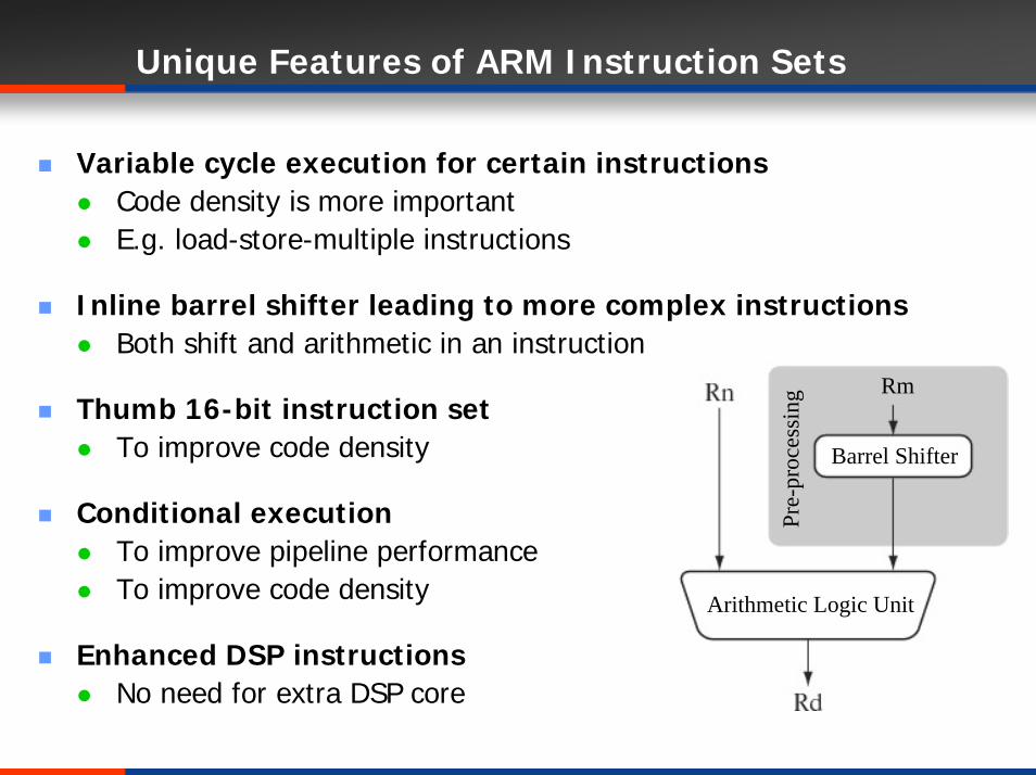
Unique Features of ARM Instruction Sets
Variable cycle execution for certain instructionsCode density is more importantE.g. load-store-multiple instructions
Inline barrel shifter leading to more complex instructionsBoth shift and arithmetic in an instruction
Thumb 16-bit instruction setTo improve code density
Conditional executionTo improve pipeline performanceTo improve code density
Enhanced DSP instructionsNo need for extra DSP core
Rm
Barrel Shifter
Arithmetic Logic Unit
Pre-
proc
essi
ng

Example of ARM-based Embedded Device
Coprocessor Interface

ARM Architecture Evolution
SA-110
ARM7TDMI
Load-store instrsfor signed and unsigned halfword / byte
System mode
Thumb instruction set (16-bit)
2
4
ARM9TDMI
SA-1110
ARM720T ARM940T
Improved ARM/Thumb state change
CLZ (Count Leading Zero) instr.
5TE
Saturated maths
DSP multiply-accumulate instructions
XScale
ARM1020E
ARM9E-S
ARM966E-S
3
Early ARM architectures
1
4T
Instruction Set Version
5TEJJazelle(Java bytecodeaccelerator)
ARM9EJ-S ARM926EJ-S
ARM7EJ-S ARM1026EJ-S
6SIMD Instructions
Multi-processing
V6 Memory architecture (VMSA)
Unaligned and mixed endian data support
ARM1136EJ-S

ARM Nomenclature
All ARM cores after the ARM7TDMI include the TDMI features
JTAGIEEE 1149.1Debugging feature
EmbeddedICE macrocellBreakpointsWatchpoints
SynthesizableProcessor core supplied as source code
ARM{x}{y}{z}{T}{D}{M}{I}{E}{J}{F}{S}
x Family (7, 8, 9, 10, 11, …)
y Memory management / protection unit
z Cache
T Thumb 16-bit decoder
D JTAG debug
M Fast Multiplier
I EmbeddedICE macrocell
EDSP Enhanced instructions (assumes TDMI)
J Jazelle
F Vector Floating-point Unit
S Synthesizable Version

ARM7 Family
32/16-bit RISC Architecture
Unified bus architectureBoth instructions and data use the same bus
3 stage pipelining Fetch / Decode / Execution
Coprocessor interface
EmbeddedICE-RT support
JTAG interface unit
Optional support for MMU (Memory Mangement Unit)Easy to port operating systems with virtual addressing capabilityE.g. ARM720T

ARM7 Family Cont
ARM9 Family
32/16-bit RISC Architecture
Harvard ArchitectureSeparate memory bus architecture
5 stage pipelining
Coprocessor interface
EmbeddedICE-RT support
JTAG interface unit
Embedded Trace Macro CellTrace instruction and data execution in real time on the processorUseful when debugging applications with time-critical segments
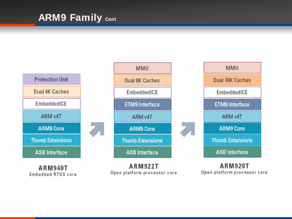
ARM9 Family Cont
ARM10 Family
6 stage pipeline
Parallel load/store unitAllow computation to continue while data transfers complete
64-bit data bus
Optional support for Vector Floating-Point7th stage in pipelineIncrease FP performance
Out-of-order completion
ExampleARM1020E► Separate 32K D+I caches► VFP (Vector Floating-Point) / MMU (Memory Management Unit)ARM1026EJ-S► Both MPU (Memory Protection Unit) and MMU

ARM1026EJ-S Block Diagram
ARM10EJ-S integer core in an ARMv5TEJ implementation
32-bit ARM16-bit Thumb8-bit Jazelle instruction set
MMUSingle TLB for both instruction and data
Memory Protection Unit (MPU)Partition external memory into 8-protection regions
Cache (I/D)Configurable to 0KB or 4-128KB
Tightly Coupled Memory (TCM)Configurable to 0KB or 4KB-1MB

ARM11 Family
8-stage pipelineLoad-store pipelineArithmetic pipeline
Parallel load/store unitAllow computation to continue while data transfers completeNon-blocking cache
64-bit data bus
Out-of-order completion
The first core to implement ARMv6SIMD (Single Instruction Multiple Data) extensions for media processing, specifically designed to increase video processing performanceDSP support (dual 16-bit MAC instructions)
ExampleARM1136J-SARM1136JF-S

ARM1136JF-S Block Diagram
ARM11 Core in an ARMv6 implementation
32-bit ARM16-bit Thumb8-bit Jazelle instruction set
Load Store Unit (LSU)Manages all load and store operationsLoad-store pipeline► Decouples loads and
stores from the MAC and ALU pipelines
Prefetch Unit
Memory systemHarvard architecture64-bit datapaths2-channel DMA into TCM

Cortex-A8
Successor to the ARM11
Dual-issue in-order execution superscalar pipeline13 stages
Support for NEON signal processing extensions64/128-bit hybrid SIMD architectureMultimedia and signal processing applications► 3D graphics, speech processing, compressed audio decoding, image
processing, telephony, sound synthesis, etc.Its own pipeline (10 stages) and register fileNeed for vectorizing compilerTarget for OpenMAX API
Thumb-2 instruction set

Cortex-A8 Architecture

Thumb-2
Exising 16-bit Thumb instructions augmented byNew 16-bit instructions for improved program flowNew 32-bit instructions derived from ARM instruction equivalents► For co-processor access, privileged instructions and special function
instructions such as SIMD
Access to equivalents for virtually all ARM instructions
Code blending is no longer requiredNo ARM/thumb modes

ARM Programming Model

Data Types
Supported Data TypesByte: 8 bits
Halfword: 16 bits (aligned to 2-byte boundaries)
Word: 32 bits (aligned to 4-byte boundaries)
Number RangeUnsigned: 0 ~ 2N – 1
Signed: -2N-1 ~ +2N-1 – 1
NotesAll data operations are performed on word quantities
Load/Store transfer B, HW, W with zero-extending and sign-extending

Memory and Memory-mapped I/O
Address Space32 bits address bus 232 Bytes from the address 0 to 232-1
Address calculations are normally performed using integer instructions
Memory-mapped I/OI/O device address defined within a single memory address space
CPU
AddressableRegion
I/O Area
0Control Reg.Status Reg.I/O Buffer
MemoryAccess
I/OOperation
4G - 1 I/O DeviceMain Memory

Byte Order
Processors can number bytes within a word so the byte with the lowest number is either the leftmost or rightmost one.
Big Endian (32bit data - 0x1234abcd)
Little Endian (32bit data - 0x1234abcd)
1212 3434 abab cdcd0
4
8
232-4
0 1 2 3
cdcd abab 3434 1212
0 1 2 3
0
4
8
232-4

Big/Little Endian
Big Endian Processor : (IBM, Motorola, SPARC)High-order-byte-first, human-friendly type
Standard on the network (TCP/IP)
Little Endian Processor: ( DEX VAX, Intel X86)Low-order-byte-first, computer-friendly type
Easy to perform the cast operation
RISC Microprocessors support Dual-Endiansince its simple instruction and operand type.
How to figure out?
int x = 1; if (*(char *) &x) == 1)
printf(“little endian”);else
printf(“big endian”);

Instruction and Operand Alignment
0 1 2 3Aligned Access
Good for performance
Byte: 4N, 4N+1, 4N+2, 4N+3
Half Word: 4N, 4N+2
Word: 4N
Unaligned AccessGood for memory usage
Half Word: 4N+1, 4N+3
Word: 4N+1, 4N+2, 4N+3
4N4N+44N+84N+C
Aligned Access
0 1 2 3
4N4N+44N+84N+C
Unligned Access
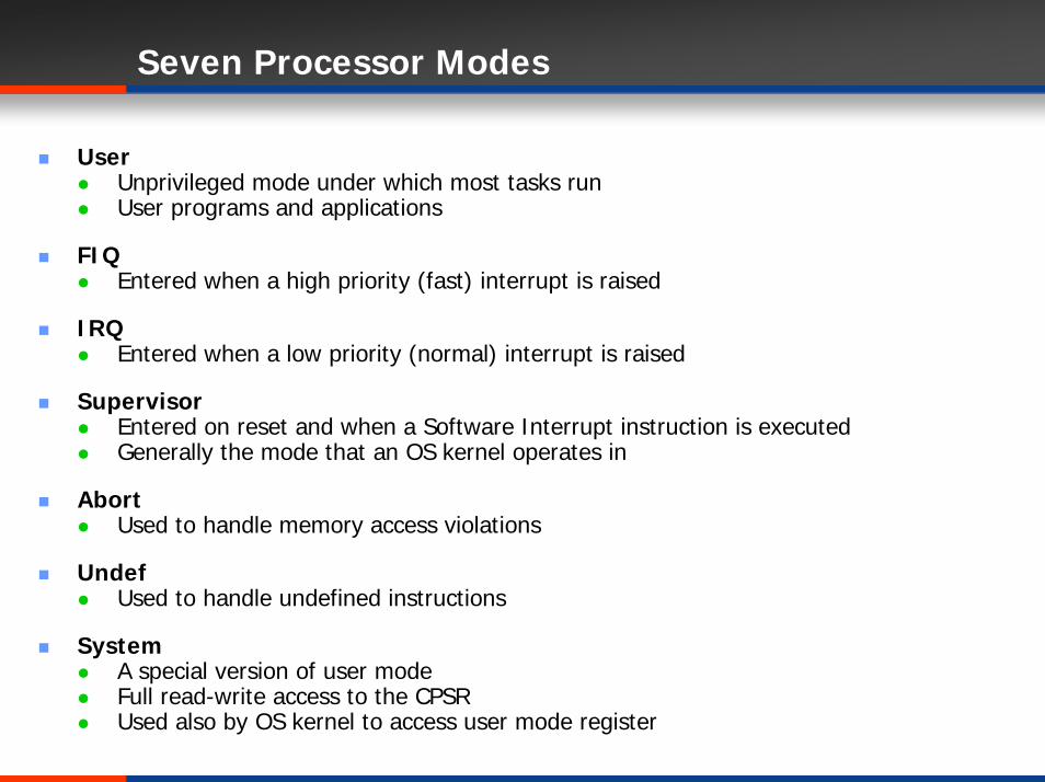
Seven Processor Modes
User Unprivileged mode under which most tasks runUser programs and applications
FIQEntered when a high priority (fast) interrupt is raised
IRQEntered when a low priority (normal) interrupt is raised
SupervisorEntered on reset and when a Software Interrupt instruction is executedGenerally the mode that an OS kernel operates in
AbortUsed to handle memory access violations
UndefUsed to handle undefined instructions
SystemA special version of user modeFull read-write access to the CPSRUsed also by OS kernel to access user mode register

Register Organization

Registers
ARM has 37 registers all of which are 32-bits long.1 dedicated PC (program counter)1 dedicated CPSR (current program status register)5 dedicated SPSR (saved program status registers)30 general purpose registers
The current processor mode governs which of several banks is accessible. Each mode can access
r0-r12: general registersr13: stack pointer (SP) r14: link register (LR)r15: program counter (PC)CPSR: current program status register
Privileged modes (except System) can also accessa particular SPSR (saved program status register)

Current Program Status Register
2731
N Z C V Q
28 67
I F T mode
1623 815 5 4 024
f s x c
UndefinedJ Undefined
Condition code flagsN = Negative result from ALU
Z = Zero result from ALU
C = ALU operation Carried out
V = ALU operation Overflowed
Sticky Overflow flag - Q flagArchitecture 5TEJ only
Indicates if saturation has occurred
J bitArchitecture 5TEJ only
J = 1: Processor in Jazelle state
Interrupt Disable bits.I = 1: Disables the IRQ.F = 1: Disables the FIQ.
T BitArchitecture xT onlyT = 0: Processor in ARM stateT = 1: Processor in Thumb state
Mode bitsSpecify the processor mode

Condition Code Flag
N (Negative/Less Than Flag)(Result < 0) (N = 1)
Z (Zero Flag)(Result == 0) (Z = 1)
C (Carry/Borrow/Extend Flag)ADD: (carry over) (C = 1)SUB: (borrow) (C = 0)Shift: (C = the bit shifted out last)
V (Overflow Flag)ADD/SUB: (Overflow) (V = 1)
e.g.FFFFFFFF
+ 00001000----------
00000FFF
N = ( ), Z = ( ), C = ( ), V = ( )

Processor States
ARM Thumb Jazelle
Instruction Size 32-bit 16-bit 8-bit
Core instructions 58 30Over 60% of Java : H/W
The rest : S/W
cpsrT=0
J=0
T=1
J=0T=0, J=1
Conditional execution Most Branch
Data processinginstructions
Barrel shifter + ALU
Separate barrel shifter and ALU
Registers 15 GPRs + PC 8 GPRs +

Processor Modes
Mode Abbrev. Privileged Bits [4:0]
Abort abt Yes 10111
10001
10010
10011
11111
11011
10000
Fast Interrupt fiq Yes
Interrupt request irq Yes
Supervisor svc Yes
System sys YesA special version of user mode
Full read-write access to CPSR
Undefined und Yes
User usr No

Program Counter (R15)
In ARM stateAll instructions are 32 bits wideAll instructions must be word alignedThe pc value stored in bits [31:2] with bits [1:0] undefined
In Thumb stateAll instructions are 16 bits wideAll instructions must be halfword alignedThe pc value stored in bits [31:1] with bit [0] undefined
In Jazelle state:All instructions are 8 bits wideProcessor performs a word access to read 4 instructions at once

Pipelines

Pipeline
The mechanism a RISC processor uses to execute instructions

Pipeline Example: ARM7
InstructionFetch
Fetch
ARMDecodeThumb-ARM
Decompress RegSelect
RegRead
Decode Execute
Shift ALU RegWrite
FetchInstruction fetch from Instruction Cache
DecodeThumb ARM DecompressARM DecodeOperand decode
ExecuteRegister Read + Shift + ALU + Write back
If Load, Store, BranchExtra cycles
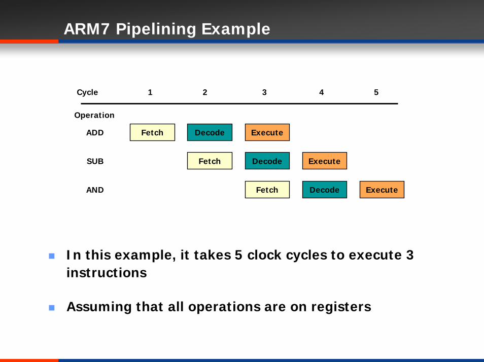
ARM7 Pipelining Example
Cycle 1 2 3 4 5
Operation
Fetch Decode ExecuteADD
Fetch Decode ExecuteSUB
Fetch Decode ExecuteAND
In this example, it takes 5 clock cycles to execute 3 instructions
Assuming that all operations are on registers

Exceptions and Interrupts

Exceptions and Interrupts
On the occurrence of an exception or interruptPC a specific memory address within the vector table
Vector tableA set of instructions that branch to specific routines to handle a particular exception or interruptLocated at 0x00000000 by default
Optionally, located at a high address in memory (at 0xffff0000)
Vector Table
Vector table can be at 0xFFFF0000 on ARM720T
and on ARM9/10 family devices
FIQ
IRQ
(Reserved)
Data Abort
Prefetch Abort
Software Interrupt
Undefined Instruction
Reset
0x1C
0x18
0x14
0x10
0x0C
0x08
0x04
0x00

Exception Vector Table
Exception Shorthand Vector address High address
Reset RESET 0x00000000 0xffff0000
Undefined instruction UNDEF 0x00000004 0xffff0004
Software interrupt SWI 0x00000008 0xffff0008
Prefetch abort PABT 0x0000000c 0xffff000c
Data abort DABT 0x00000010 0xffff0010
Reserved - 0x00000014 0xffff0014
Interrupt request IRQ 0x00000018 0xffff0018
Fast interrupt request FIQ 0x0000001c 0xffff001c

Exception Handling
When an exception occurs, the ARM:Copies CPSR into SPSR_<mode>Sets appropriate CPSR bits ► Change to ARM state► Change to exception mode ► Disable interrupts (if appropriate)Stores the return address in LR_<mode>Sets PC to vector address
To return, exception handler needs to:Restore CPSR from SPSR_<mode>Restore PC from LR_<mode>
This can only be done in ARM state.

Exception Handling Operation
ResetWhen the processor’s Reset input is asserted► CPSR ⇐ Supervisor + I + F► PC ⇐ 0x00000000
Undefined InstructionIf an attempt is made to execute an instruction that is undefined► LR_undef ⇐ Undefined Instruction Address + #4► PC ⇐ 0x00000004, CPSR ⇐ Undefined + I► Return with : MOVS pc, lr
Prefetch AbortInstruction fetch memory abort, invalid fetched instruction► LR_abt ⇐ Aborted Instruction Address + #4, SPSR_abt ⇐ CPSR► PC ⇐ 0x0000000C, CPSR ⇐ Abort + I► Return with : SUBS pc, lr, #4
Exception Handling Operation
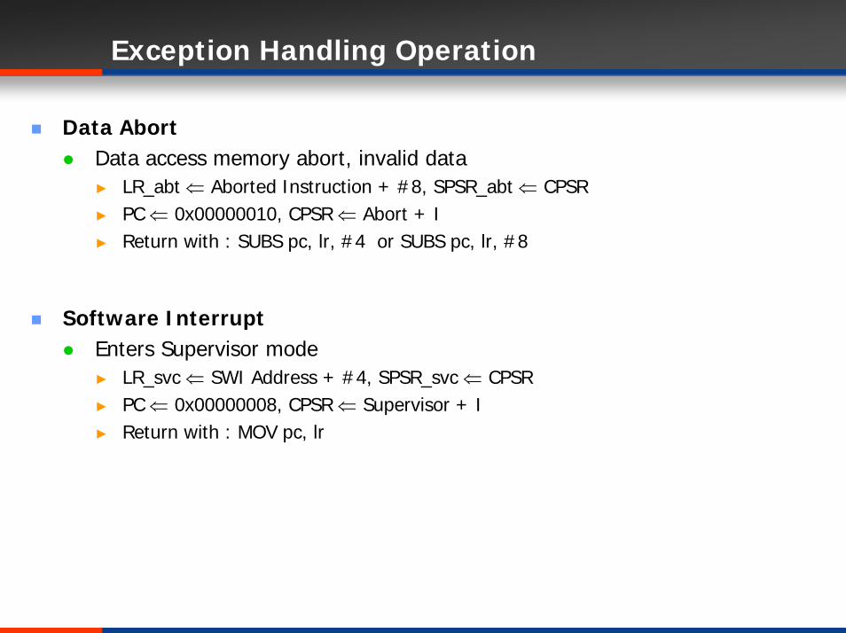
Data AbortData access memory abort, invalid data ► LR_abt ⇐ Aborted Instruction + #8, SPSR_abt ⇐ CPSR► PC ⇐ 0x00000010, CPSR ⇐ Abort + I► Return with : SUBS pc, lr, #4 or SUBS pc, lr, #8
Software InterruptEnters Supervisor mode ► LR_svc ⇐ SWI Address + #4, SPSR_svc ⇐ CPSR► PC ⇐ 0x00000008, CPSR ⇐ Supervisor + I► Return with : MOV pc, lr

Exception Handling Operation
Interrupt RequestExternally generated by asserting the processor’s IRQ input► LR_irq ⇐ PC - #4, SPSR_irq ⇐ CPSR► PC ⇐ 0x00000018, CPSR ⇐ Interrupt + I► Return with : SUBS pc, lr, #4
Fast Interrupt RequestExternally generated by asserting the processor’s FIQ input► LR_fiq ⇐ PC - #4, SPSR_fiq ⇐ CPSR► PC ⇐ 0x0000001C, CPSR ⇐ Fast Interrupt + I + F► Return with : SUBS pc, lr, #4 ► Handler @0x1C speeds up the response time

ARM Core

Core Extensions
Cache
TCM (Tight Coupled Memory)
Memory Management HardwareNon-protected Memory
MPU (Memory Protection Unit)
MMU (Memory Management Unit)
Coprocessors

Cache
Improves the overall system performance
< A simplified Von-Neumann architecture with cache >

TCM
Improves deterministic real-time response
Appears as memory in the address map
< A simplified Harvard architecture with TCMs >

Memory Management Hardware
Non-protected memorySmall embedded systems that require no protection from rouge application
MPU Defines memory regions and access permissionsLimited protection
MMUMore sophisticated platform operating systems that support multitaskingFull protection

MPU
DevicesI/O
Region 4
Task 3
Task 2
Task 1
SystemShared
SystemProtected
Region 2
Region 3
Region 1
0x110000000xFFFFFFFF
0x000380000x10000000
0x00030000
0x00028000
0x000200000x00020000
0x00015000
0x000100000x00000000

Coprocessors
Extends the processing features of a core by extending the instruction set or by providing configuration registers
Coprocessor instructions are processed in the decode stage
If found, offered to the relevant coprocessor
Vector Floating-Point (VFP) operations
CP10/CP11
System Control Coprocessor
CP15
Controls the cache, TCMs, MPU, MMU

ARM Instruction Set
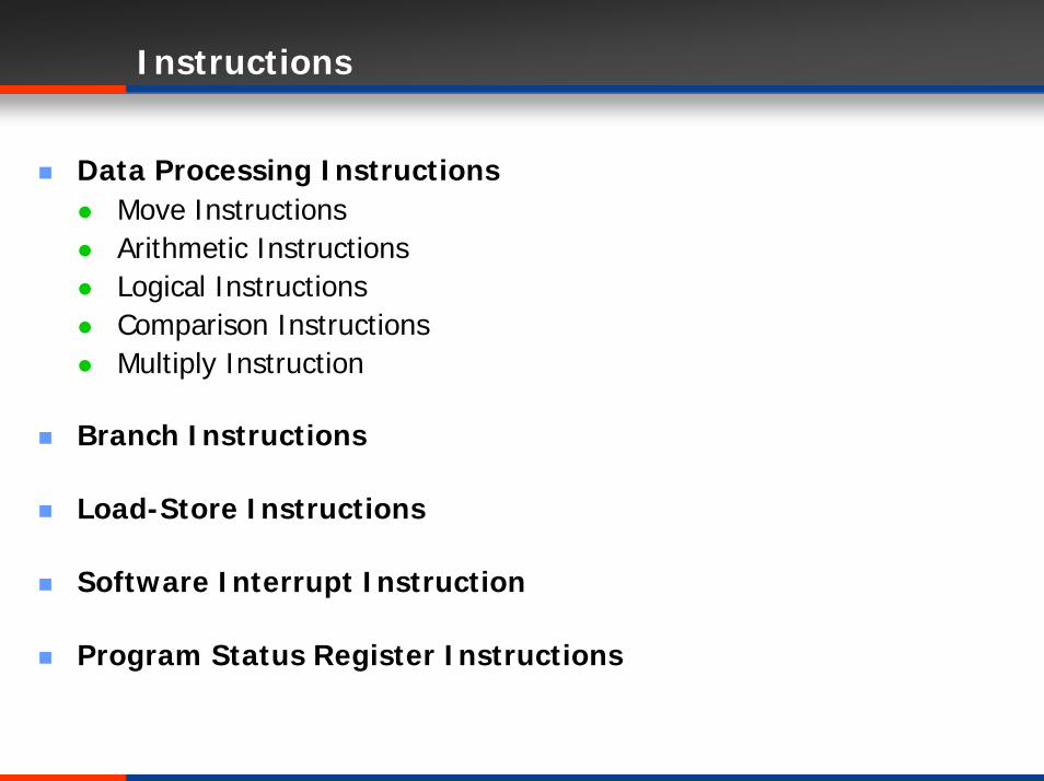
Instructions
Data Processing InstructionsMove InstructionsArithmetic InstructionsLogical InstructionsComparison InstructionsMultiply Instruction
Branch Instructions
Load-Store Instructions
Software Interrupt Instruction
Program Status Register Instructions

ARM Instructions
Encoded in a 32-bit word
OP code + two or three registers
Executed in a cycle
8, 16, 32 bit memory access Memory access only through LOAD and STORE instructions
Conditional execution of instructionsAll instructions are conditionally executedThe S suffix on a data processing instruction make the flags in the CPSR updated
Condition
31
OP code
28 27 20 19 16 15 12 11 4 3 0
Rn Rd Other info Rm
Conditional Execution
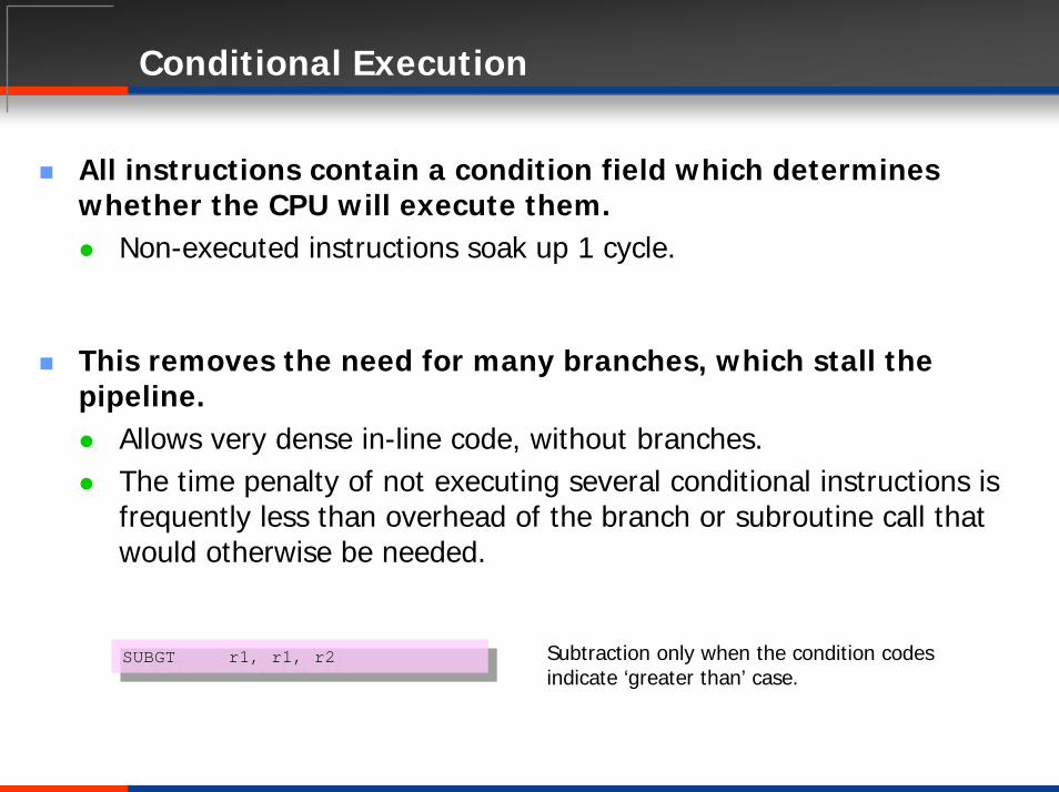
All instructions contain a condition field which determines whether the CPU will execute them.
Non-executed instructions soak up 1 cycle.
This removes the need for many branches, which stall the pipeline.
Allows very dense in-line code, without branches.The time penalty of not executing several conditional instructions is frequently less than overhead of the branch or subroutine call that would otherwise be needed.
SUBGT r1, r1, r2SUBGT r1, r1, r2 Subtraction only when the condition codes indicate ‘greater than’ case.

The Condition Field
31 28 27 0
Cond Reserved
Cond Mnemonic Meaning Condition flag state
Equal Z = 1
Z = 0
C = 1
C = 0
0100 MI Minus/Negative N = 1
0101 PL Plus/Positive or Zero N = 0
1000 HI Unsigned higher C=1 & Z=0
1001 LS Unsigned lower or same C=0 | Z=1
1010 GE Signed >= N==V
1011 LT Signed < N!=V
1100 GT Signed > Z==0,N==V
1101 LE Signed <= Z==1 or N!=V
1110 AL Always
1111 (NV) Unpredictable
0110 VS Overflow O = 1
0111 VC No overflow O = 0
Not Equal
Carry set / unsigned >=
Carry clear / unsigned <
0000 EQ
0001 NE
0010 CS/HS
0011 CC/LO

Using and updating the Condition Field
To execute an instruction conditionally, simply postfix it with the appropriate condition
For example an add instruction takes the form:► ADD r0,r1,r2 ; r0 = r1 + r2 (ADDAL)
To execute this only if the zero flag is set:► ADDEQ r0,r1,r2 ; If zero flag set then…
; ... r0 = r1 + r2
Data processing operations do not affect the condition flags.
To cause the condition flags to be updated, the instruction needs to be postfixed with an “S”.
For example to add two numbers and set the condition flags:► ADDS r0,r1,r2 ; r0 = r1 + r2
; ... and set flags

Conditional Execution Example
gcd CMP r1, r2
BEQ complete
BLT lessthan
SUB r1, r1, r2
B gcd
lessthan SUB r2, r2, r1
B gcd
complete . . .
gcd CMP r1, r2
BEQ complete
BLT lessthan
SUB r1, r1, r2
B gcd
lessthan SUB r2, r2, r1
B gcd
complete . . .
while (a != b) {
if (a > b) a -= b;
else b -= a;
}
while (a != b) {
if (a > b) a -= b;
else b -= a;
}
gcd CMP r1, r2
SUBGT r1, r1, r2
SUBLT r2, r2, r1
BNE gcd
. . .
gcd CMP r1, r2
SUBGT r1, r1, r2
SUBLT r2, r2, r1
BNE gcd
. . .
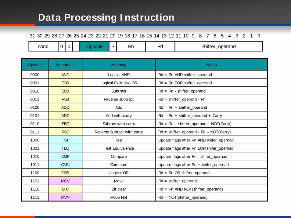
Data Processing Instruction
31 30 29 28 27 7 6 5 4 026 25 24 23 22 21 20 19 18 17 16 15 14 13 12 11 810 9 3 2 1
cond 0 0 I SOpcode Rn Shifter_operandRd
Opcode Mnemonic Meaning Action
Logical AND Rd = Rn AND shifter_operand
Rd = Rn EOR shifter_operand
Rd = Rn - shifter_operand
Rd = shifter_operand - Rn
0100 ADD Add Rd = Rn + shifter_operand
0101 ADC Add with carry Rd = Rn + shifter_operand + Carry
1000 TST Test Update flags after Rn AND shifer_opernad
1001 TEQ Test Equivalence Update flags after Rn EOR shifer_opernad
1010 CMP Compare Update flags after Rn - shifer_opernad
1011 CMN Commom Update flags after Rn + shifer_opernad
1100 ORR Logical OR Rd = Rn OR shifter_operand
1101 MOV Move Rd = shifter_operand
1110 BIC Bit clear Rd = Rn AND NOT(shifter_operand)
1111 MVN Move Not Rd = NOT(shifter_operand)
0110 SBC Subract with carry Rd = Rn – shifter_operand – NOT(Carry)
0111 RSC Reverse Subract with carry Rd = shifter_operand - Rn – NOT(Carry)
Logical Exclusive OR
Subtract
Reverse subtract
0000 AND
0001 EOR
0010 SUB
0011 RSB

MOVE Instruction : MOV
MOV: MoveMove a 32-bit value to a register
Syntax1. MOV<cond>{S} <Rd>, #<rotated_immed>
2. MOV<cond>{S} <Rd>, <Rm> {, <shift>}
ExamplesMOV r0, #0xff000000 r0 = 0xff000000
MOV pc, lr pc = lr
MOV r0, r1, LSL#2 r0 = r1 << 2

MOVE Instruction : MVN
MVN : Move NOTMove the NOT of the 32-bit value into a register
Syntax1. MVN<cond>{S} <Rd>, #<rotated_immed>
2. MVN<cond>{S} <Rd>, <Rm> {, <shift>}
ExamplesMVN r0, #0xff000000 r0 = 0x00ffffff
MVN r0, r1 r0 = ~r1
MVN r0, r1, LSL#2 r0 = ~(r1*4)

Barrel Shifter
To shift the 32-bit binary pattern in one of the source registers left or right
Pre-processing or shift occurs within the cycle time of the instruction
Data processing instruction not using the barrel shifter
MUL (multiply)CLZ (count leading zeros)QADD (signed saturated 32-bit add)Etc.
Rm
Barrel Shifter
Result N
Arithmetic Logic Unit
Pre-
proc
essi
ng
No
Pre-
proc
essi
ng

Barrel Shifter Operations
Mnemonic Description Shift Result Shift Amount y
LSL Logical shift left x LSL y x << y #0-31 or Rs
LSR Logical shift right x LSR y (unsigned) x >> y #1-32 or Rs
ASR Arithmetic right shift x ASR y (signed) x >> y #1-32 or Rs
ROR Rotate right x ROR y ((unsigned) x >> y) | ( x << (32-y)) #1-31 or Rs
RRX Rotate right extended x RRX y (c flag << 31) | ((unsigned) x >> 1) none

Logical Shift (LSL, LSR)
Rotate Right (ROR)
Rotate Right Extension (RRX)
bn-1 bn-2 … b1 b0
00
shift rightB ← LSR B
shift leftB ← LSL B
0 bn-1 … b2 b1 bn-2 bn-3 … b0 0
bn-1 bn-2 … b1 b0
shift right: B ← ROR B
b0 bn-1 … b2 b1
bn-1 bn-2 … b1 b0C
Shifts

Arithmetic Shift for Signed Binary NumbersArithmetic shift right (ASR) : B ← ASR B
► divide by 2
6/2 = ASR 6 : 0110 -> 0011 (3)
-6/2 = ASR –6 : 1010 -> 1101 (-3)
bn-1 bn-2 … b1 b0
bn-1 bn-1 … b2 b1
sign bit
Shifts

Arithmetic Instruction : ADD
ADD : AddAdd two 32-bit values
Syntax1. ADD<cond>{S} <Rd>, <Rn>, #<rotated_immed>2. ADD<cond>{S} <Rd>, <Rn>, <Rm> {, <shift>}
ExamplesADD r0, r1, #4 r0 = r1 + 4ADD r0, r0, r0, LSL#2 r0 = r0 + r0*4
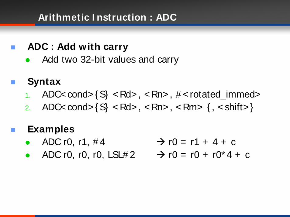
Arithmetic Instruction : ADC
ADC : Add with carryAdd two 32-bit values and carry
Syntax 1. ADC<cond>{S} <Rd>, <Rn>, #<rotated_immed>2. ADC<cond>{S} <Rd>, <Rn>, <Rm> {, <shift>}
ExamplesADC r0, r1, #4 r0 = r1 + 4 + cADC r0, r0, r0, LSL#2 r0 = r0 + r0*4 + c

Arithmetic Instruction : SUB
SUB : SubtractSubtract two 32-bit values
Syntax 1. SUB<cond>{S} <Rd>, <Rn>, #<rotated_immed>2. SUB<cond>{S} <Rd>, <Rn>, <Rm> {, <shift>}
ExamplesSUB r0, r0, #1 r0 = r0 - 1SUB r0, r0, r0, LSL#2 r0 = r0 - r0 * 4

Arithmetic Instruction : SBC
SBC : Subtract with carrySubtract with carry of two 32-bit values
Syntax 1. SBC<cond>{S} <Rd>, <Rn>, #<rotated_immed>2. SBC<cond>{S} <Rd>, <Rn>, <Rm> {, <shift>}
ExamplesSBC r0, r0, #1 r0 = r0 - 1 - (~c) SBC r0, r1, r2 r0 = r1 - r2 - (~c)

Arithmetic Instruction : RSB
RSB : Reverse SubtractReverse subtract of two 32-bit values
Syntax1. RSB<cond>{S} <Rd>, <Rn>, #<rotated_immed>2. RSB<cond>{S} <Rd>, <Rn>, <Rm> {, <shift>}
ExampleRSB r0, r0, #0 r0 = -r0 RSB r0, r1, r1, LSL#3 r0 = r1*7
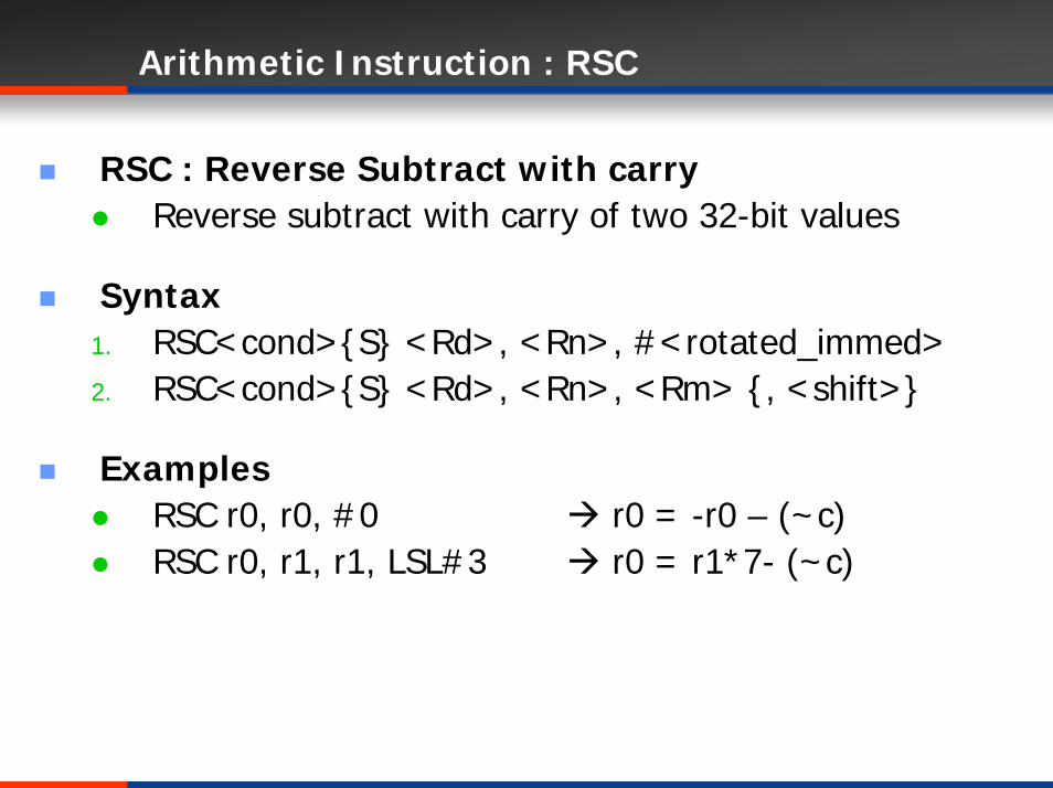
Arithmetic Instruction : RSC
RSC : Reverse Subtract with carryReverse subtract with carry of two 32-bit values
Syntax1. RSC<cond>{S} <Rd>, <Rn>, #<rotated_immed>2. RSC<cond>{S} <Rd>, <Rn>, <Rm> {, <shift>}
ExamplesRSC r0, r0, #0 r0 = -r0 – (~c) RSC r0, r1, r1, LSL#3 r0 = r1*7- (~c)

Logical Instruction : AND
ANDLogical bitwise AND of two 32-bit values
Syntax1. AND<cond>{S} <Rd>, <Rn>, #<rotated_immed>
2. AND<cond>{S} <Rd>, <Rn>, <Rm> {, <shift>}
ExampleAND r0, r0, #0xff r0 = r0 & 0xff

Logical Instruction : ORR
ORRLogical bitwise OR of two 32-bit values
Syntax 1. ORR<cond>{S} <Rd>, <Rn>, #<rotated_immed>
2. ORR<cond>{S} <Rd>, <Rn>, <Rm> {, <shift>}
ExampleORR r0, r0, #0xff r0 = r0 | 0xff
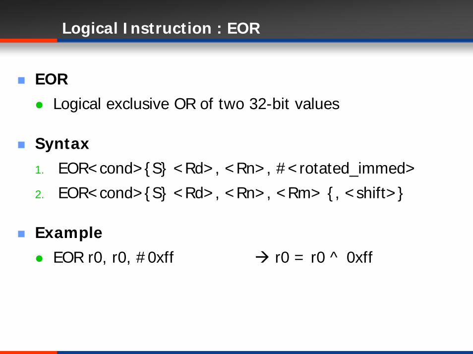
Logical Instruction : EOR
EORLogical exclusive OR of two 32-bit values
Syntax1. EOR<cond>{S} <Rd>, <Rn>, #<rotated_immed>
2. EOR<cond>{S} <Rd>, <Rn>, <Rm> {, <shift>}
ExampleEOR r0, r0, #0xff r0 = r0 ^ 0xff

Logical Instruction : BIC
BIC : Bit ClearLogical bit clear (AND NOT)
Syntax1. BIC<cond>{S} <Rd>, <Rn>, #<rotated_immed>
2. BIC<cond>{S} <Rd>, <Rn>, <Rm> {, <shift>}
ExampleBIC r0, r0, #0x1<<22

Comparison Instruction : CMP
CMP : CompareUpdates the CPSR flag bits
Not affect other registers
Flags set as a result of Rn - N
Syntax 1. CMP<cond> <Rn>, #<rotated_immed>
2. CMP<cond> <Rn>, <Rm> {, <shift>}
ExampleCMP r0, r1 r0 - r1

Comparison Instruction : CMN
CMNCompare negatedUpdates the CPSR flag bitsNot affect other registersFlags set as a result of Rn + N
Syntax 1. CMN<cond> <Rn>, #<rotated_immed>2. CMN<cond> <Rn>, <Rm> {, <shift>}
ExampleCMN r0, #3 r0 + 3 = r0 – (-3)

Comparison Instruction : TST
TSTTest bits of a 32-bit value
Flags set as a result of Rn & N
Syntax1. TST<cond> <Rn>, #<rotated_immed>
2. TST<cond> <Rn>, <Rm> {, <shift>}
ExampleTST r0, #0xff r0 & 0xff

Comparison Instruction : TEQ
TEQ : Test EquivalenceTest for equality of two 32-bit values
Flags set as a result of Rn ^ N
Syntax 1. TEQ<cond> <Rn>, #<rotated_immed>
2. TEQ<cond> <Rn>, <Rm> {, <shift>}
ExampleTEQ r0, #1 r0 ^ 1

Multiply : MUL
MUL : MultiplyMultiply the contents of a pair of registers
Syntax1. MUL<cond>{S} <Rd>, <Rm>, <Rs>
ExampleMUL r0, r1, r2 r0 = r1 * r2

Multiply : MLA
MLA : Multiply and AddMultiply and accumulate the contents of a pair of registers
Syntax1. MLA<cond>{S} <Rd>, <Rm>, <Rs>, <Rn>
ExampleMLA r0, r1, r2, r3 r0 = r1 * r2 + r3

Multiply : Long (64-bit) Multiply
Long MultiplyMultiply singed/unsigned 64-bit value
Syntax<instr><cond>{S} <RdLo>, <RdHi>, <Rm>, <Rs>
ExampleSMLAL r0, r1, r2, r3 [r0,r1] = [r0,r1] + r2 * r3
SMULL r0, r1, r2, r3 [r0,r1] = r2 * r3
UMLAL r0, r1, r2, r3 [r0,r1] = [r0,r1] + r2 * r3
UMULL r0, r1, r2, r3 [r0,r1] = r2 * r3

Branch Instructions
Changes the flow of executionEx) subroutines, if-then-else, loops
InstructionsB branch
BL branch and link
BX branch exchange
BLX branch exchange with link
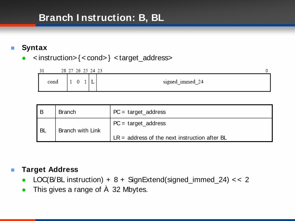
Branch Instruction: B, BL
Syntax <instruction>{<cond>} <target_address>
Target AddressLOC(B/BL instruction) + 8 + SignExtend(signed_immed_24) << 2This gives a range of ± 32 Mbytes.
B Branch PC = target_address
BL Branch with LinkPC = target_address
LR = address of the next instruction after BL
Branch Instruction: B, BL
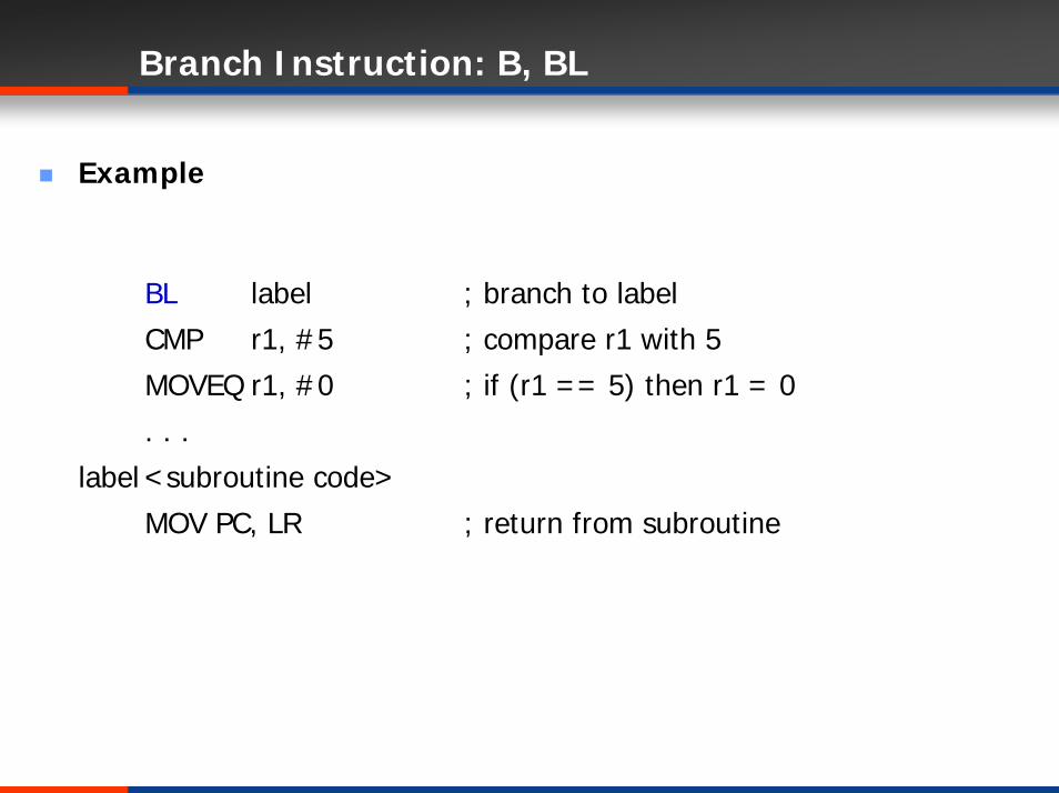
Example
BL label ; branch to label
CMP r1, #5 ; compare r1 with 5
MOVEQ r1, #0 ; if (r1 == 5) then r1 = 0
. . .
label <subroutine code>
MOV PC, LR ; return from subroutine
Branch instructions
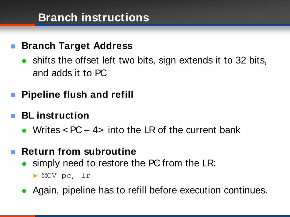
Branch Target Addressshifts the offset left two bits, sign extends it to 32 bits, and adds it to PC
Pipeline flush and refill
BL instruction Writes <PC – 4> into the LR of the current bank
Return from subroutinesimply need to restore the PC from the LR:► MOV pc, lr
Again, pipeline has to refill before execution continues.

Load-Store Instructions
Transfer data between memory and processor registers
Three typesSingle-register transfer► LDR/STR
Multiple-register transfer► LDM/STM
Swap data► SWP

Single Register Transfer
Moves a single data item in and out of a register
Signed/unsigned words(32-bit), halfwords(16-bit), and bytes

Memory Addressing Modes
Memory AccessIndexed Addressing Mode
Effective Address A signed offset + base register (Rn)► A signed offset = immediate or register (Rm)
ExamplesLDR R1, [R0, #10] Rd [R2 + #10]LDR R1, [R2] R1 [R2]
STR R1, [R2] [R2] R1
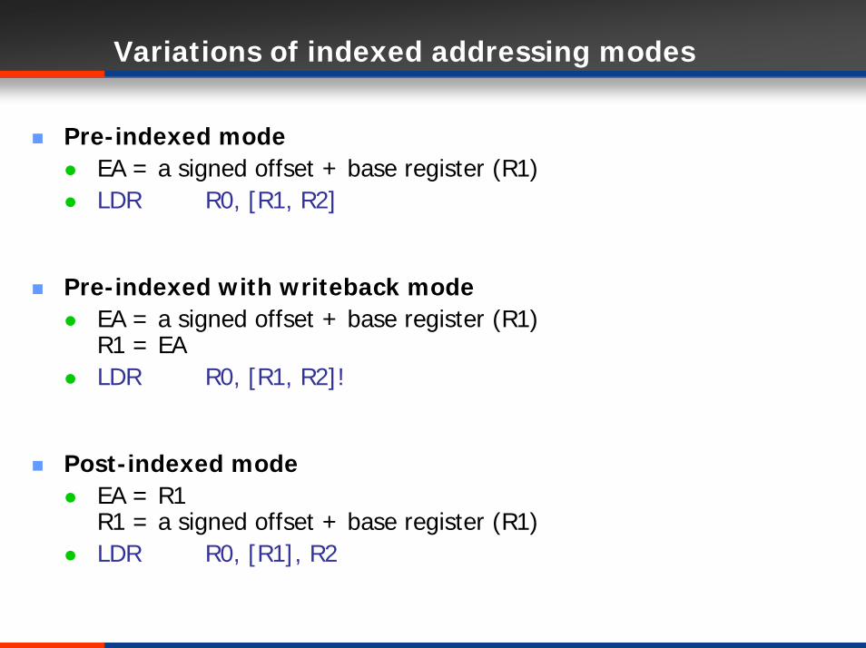
Variations of indexed addressing modes
Pre-indexed modeEA = a signed offset + base register (R1)LDR R0, [R1, R2]
Pre-indexed with writeback modeEA = a signed offset + base register (R1)R1 = EALDR R0, [R1, R2]!
Post-indexed modeEA = R1R1 = a signed offset + base register (R1)LDR R0, [R1], R2

Example: Memory Addressing Modes
•100 = 25 x 4
•1000
•word (4 bytes)
•(a) Post-indexed addressing with writeback
•25
•2008
•Base register
•(b) Pre-indexed addressing with writeback
•2012
•Base register (Stack pointer)
•*•*•*
•6
•1100
•R2
•R0
•-17
•*•*•*
•321•1200
•100 = 25 x 4
•1000
•Offset register
•R10
•R5
•27•27
•-•2012
•after execution of
•Memory•address
•Push instruction
•Load instruction:
•LDR R1,[R2],R10,LSL #2
•Push instruction:
•STR R0,[R5,#-4]!
•52 = offset
•1000
•word (4 bytes)
• ITEM = 1060 •Operand
• Memory• address
•updated [PC] = 1008
•(a) Relative addressing mode
•1000
•200 = offset
•1000
•1200
•Base register
•(b) Pre-indexed addressing mode
•200
•Offset register
•*•*•*
•*•*•*
•*•*•*
•*•*•*
•*•*•*
•LDR R1, ITEM
•1004
•1008 •-
•-
•STR R3, [R5, R6] •R5
•R6
•Operand

Multiple Register Transfer
Transfer multiple registers between memory and the processor in a single instruction
Non-RISC Style
Can increase interrupt latencyARM does not usually interrupt instructions while executing
SyntaxLDM{<cond>}<addressing mode> Rn{!}, <regs>{^}!: register updated after the operation^: move CPSR altogetherAddressing modes► IA (Increment After)► IB (Increment Before)► DA (Decrement After)► DB (Decrement Before)
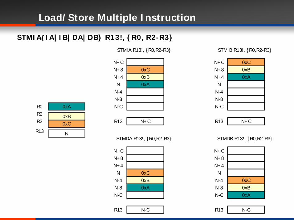
Load/Store Multiple Instruction
STMIA{IA|IB|DA|DB} R13!, {R0, R2-R3}
STMIA R13!, {R0,R2-R3} STMIB R13!, {R0,R2-R3}
0xANN+4N+8N+C
0xA
R3 0xC
R2 0xB
R0
NR13
0xB0xC
N-4N-8N-C
0xAN
N+4N+8N+C
0xB0xC
N-4N-8N-C
N+C N+CR13 R13
STMDA R13!, {R0,R2-R3} STMDB R13!, {R0,R2-R3}
0xA
NN+4N+8N+C
0xB0xC
N-4N-8N-C 0xA
NN+4N+8N+C
0xB0xCN-4
N-8N-C
N-C N-CR13 R13

Stack Push Operations
Ascending Stack
Full Ascending (FA) Stack Empty Ascending (EA) Stack
NN+4N+8
NN+4N+8
N+C N+CSP
STMEA (STMIA)
SP
STMFA (STMIB)
Descending Stack
EFull Descending (FD) Stack mpty Descending (ED) Stack
NN+4N+8
SP
NN+4N+8
SPN+C N+C
STMFD (STMDB) STMED (STMDA)

Using BL, STM and LDM
In ATPCS(ARM Thumb Procedure Call Standard)The stack implementation is full-descending, with the current extent of the stack held in the register SP (r13).
Register r4-r10 is used for variables
r0-r3 is used for function parameters or scratch register
r0 contains return value
function1......add r0, r1, r2bl function2and r0, r1, r2......
function2stmfd sp!, {r4-r6, lr}mov r5, #5mov r6, #6add r4, r5, r6add r4, r0mov r0, r4ldmfd sp!, {r4-r6, pc}

Atomic operation of a memory read followed by a memory write which moves byte or word quantities between registers and memory.
Syntax:SWP{<cond>}{B} Rd, Rm, [Rn]
Thus to implement an actual swap of contents make Rd = Rm.
The compiler cannot produce this instruction.
Rm Rd
Rn
32
1
temp
Memory
pointer
New Val
Old Val
Old Val
Swap and Swap Byte Instructions

Software Interrupt : SWI
Causes a software interrupt exceptionProvides a mechanism for applications to call operating system routines
Implementing a user-defined instruction
SyntaxSWI{<cond>} SWI_number
OperationLR_svc = address of instruction following the SWISPSR_svc = CPSRPC = Vector_Table[2]; offset 8CPSR_mode= SVCCPSR_I = 1 (mask IRQ interrupts)

SWI Handler
2831 2427 0
Cond 1 1 1 1 Comment field (ignored by Processor)
Condition Field
23
SWI_number<SWI instruction> AND NOT (0xff000000)The location of <SWI instruction> is calculated based on the link register LR
swi_handlerSTMFD sp!, {r0-r12, lr}LDR r10, [lr, #-4]BIC r10, r10, #0xff000000BL service_routine ; now r10 has the SWI
numberLDMFD sp!, {r0-r12, pc}^

PSR Instructions
MRS and MSR allow contents of CPSR/SPSR to be transferred from appropriate status register to a general purpose register.
All of status register, or just the flags, can be transferred.
SyntaxMRS{<cond>} Rd, <CPSR|SPSR>MSR{<cond>} <CPSR|SPSR>, RmMSR{<cond>} <CPSR|SPSR>_<fields>, RmMSR{<cond>} <CPSR|SPSR>_<fields>, #imm► The immediate must be 32 bit long, of which the 4 msbs are written to
the flag bits
ExampleMRS r1, CPSRBIC r1, r1, #0x80 ; enables IRQ interruptsMSR CPSR_c, r1

Using MRS and MSR
Currently reserved bits, may be used in future, therefore:they must be preserved when altering PSRthe value they return must not be relied upon when testing other bits.
Thus read-modify-write strategy must be followed when modifying any PSR:
Transfer PSR to register using MRSModify relevant bitsTransfer updated value back to PSR using MSR
NoteIn User Mode, all bits can be read but only the flag bits can be written to.
2731
N Z C V Q
28 67
I F T mode
1623 815 5 4 024
f s x c
UndefinedJ Undefined

Using MRS and MSR
This codes is from stack initialization of boot code
...UNDEFMODE EQU 0x1bMODEMASK EQU 0x1fNOINT EQU 0xc0UndefStack EQU (_STACK_BASEADDRESS-0x2400) ;0x31ff5c00
...
InitStacksmrs r0,cpsrbic r0,r0,#MODEMASKorr r1,r0,#UNDEFMODE|NOINTmsr cpsr_cxsf,r1 ;UndefModeldr sp,=UndefStack
...
Coprocessors

Coprocessors
Supports 16 coprocessorsProvides additional computation capabilityControls the memory subsystem including caches and memory management
Three types of coprocessor instructionsCoprocessor data processing
Coprocessor (to/from ARM) register transfers
Coprocessor memory transfers (load and store to/from memory)
A coprocessor may be implemented in hardware
in software (via the undefined instruction exception)
in both (common cases in hardware, the rest in software)

Coprocessor 15 Instruction
CP15 - System control coprocessorConfigures the processor coreHas a set of dedicated registers to store configuration information► Cache configuration and management► Tightly-Coupled Memory (TCM) configuration and management► Memory Management Unit (MMU) configuration and management► DMA control► Debug accesses to the caches and Translation Lookaside Buffer (TLB)► System performance monitoring.
SyntaxCDP{<cond>} cp#, opcode1, Cd, Cn{, opcode2}<MRC|MCR>{<cond>} cp#, opcode1, Cd, Cn, Cm{, opcode2}<LDC|STC>{<cond>} cp#, Cd, addressing
ExampleMRC p15, 0, r1, c1, c0, 0 ; CP15 c1 r1

Sample use of CP15 in ARM1136
Thumb Instructions

The Thumb Concept
16-bit Re-encoded Subset of the ARM Instruction SetBetter code density than ARM Increase performance of ARM system using 16-bit bus
Use Advantages of 32-bit Architecture with RestrictionInternally, 16-bit instructions are remapped into 32-bit ones► ARM7TDMI: Decompress logic during decoding stage► ARM9TDMI: Separated decoding logic for fast pipelining
Example: ADD Rd, #immediate
1 1 1 0 0 0 0 0 8-bit immediate0 0 1 10 1 0 0 0 Rd 0 Rd
0 0 1 8-bit immediate1 0 Rd
Always ConditionCode
Major op-code:Move/compare/add/subWith immediate value
Minor op-code:ADD
Destination andSource Register
Immediate value
ARM Code
Thumb Code

Thumb Code in Action
if(x>=0)return x;
elsereturn –x;
Simple C Routine
iabs CMP r0, #0RSBLT r0, r0, #0MOV pc, lr
ARM Assemblyiabs CMP r0, #0
BGE returnNEG r0, r0
return MOV pc, lr
Thumb Assembly
Code Instructions Size(Byte) Normalized 16-bit bus 32-bit bus6 access 3 access
4 access4 access
1.0
0.67
12
8ARM 3
Thumb 4

Thumb Characteristics
16 bit instructionsSome of 32 bit ARM instructions are not implementedDecoded into equivalent 32-bit instructions in ARM
Adv.Small program codes (70% of ARM codes)Faster execution (130% faster in 16-bit memory system)Less energy consumption
Disadv.More instructions► Use ARM instructions for high speed operationWhen entering into an exception mode, ARM mode is enabled. Less flexible

Thumb State Registers
User & System FIQ IRQ Supervisor Abort Undef
R0 R0 R0 R0 R0 R0R1 R1 R1 R1 R1 R1R2 R2 R2 R2 R2 R2R3 R3 R3 R3 R3 R3R4 R4 R4 R4 R4 R4R5 R5 R5 R5 R5 R5R6 R6 R6 R6 R6 R6R7 R7 R7 R7 R7 R7SP SP_fiq SP_irq SP_svc SP_abt SP_undLR LR_fiq LR_irq LR_svc LR_abt LR_und
Program CounterPC PC PC PC PC PC
Program Status RegisterCPSR CPSR CPSR CPSR CPSR CPSR
SPSR_fiq SPSR_irq SPSR_svc SPSR_abt SPSR_fiq

Mapping of Thumb Regs onto ARM Regs
Thumb State ARM State
R0~R7
Access viaSpecial instruction
Stack Pointer(SP)
Link Register(LP)
Program Counter(PC)
CPSR
SPSR
R0~R7
R8~R12
Stack Pointer(R13)
Link Register(R14)
Program Counter(R15)
CPSR
SPSR

State Transition between ARM and Thumb
......
ADR R0, Into_T+1
BX R0
CODE16
Into_T
......
ADR R5, Back_A
BX R5
ALIGN
CODE32
Back_A
......
Switching State Example
ARM StateARM State Thumb StateThumb State
1. BX Instruction2. Return from Exception Mode
if exception occurs in Thumb State
1. BX Instruction2. Taking an Exception

Branch Instructions
B<cond> <target_address>Forward or backward branches of up to 256 bytes
B <target _address>Forward or backward branches of up to 2KB
BL <target_address>Branch and Link: forward or backward up to 4MB
2 instruction implementation
BX <Rm>Branch and Exchange: branch with address in Rm
Optionally, switch to ARM state

Data Processing Instructions
Addition, Subtraction, MultiplicationADC|SBC|CMN|CMP|NEG|MUL Rd, RmADD|SUB Rd, Rn, RmADD|SUB Rd, Rn, #0 ~ 7ADD|SUB|CMP Rd, #0 ~255
Bit-wise Operation AND|BIC|EOR|ORR|TST|MOV|MVN Rd, RmMOV Rd, #0 ~ 255
Shift OperationASR|LSR Rd, Rm, #1 ~ 32ASR|LSL|LSR|ROR Rd, RsLSL Rd, Rm, #0 ~ #31
High Register InstrucitonsMOV|ADD|CMP Rd, RnADD|SUB SP, #0 ~ 508ADD Rd, SP|PC, #0 ~ 1020

Load/Store and SWI Instructions
LDR|LDRH|LDRB|STR|STRH|STRB <Rd>, [<Rn>, #<offset_5>]Word scaled by 4, HW scaled by 2
LDR|LDRH|LDRSH|LDRB|STR|STRH|STRB Rd, [Rn, Rm]
LDR Rd, [PC, #<offset_8>]Scaled by 4
LDR|STR Rd, [SP, #<offset_8>]Scaled by 4
LDMIA|STMIA Rn!, <registers>
PUSH {<registers>} STMDB SP!, <registers>
POP {<registers>} LDMIA SP!, <registers>
SWI <immed_8>

Pseudo Instructions

ARM Pseudo-Instructions
ADR/ADRLLoad a program-relative or register-relative address into a registerADR: generates one instruction (ADD or SUB)► +/-255 bytes for non-aligned address► +/-1020 bytes for word-aligned addressADRL: generates two data processing instructions► +/-64KB for non-aligned address► +/-256KB for word-aligned address
SyntaxADR{<cond>}{L} <Rd>, <expr><expr> := a program-relative or register-relative expression
Examplestart MOV r0,#10
ADR r4, start ; => SUB r4, pc, #0xC
ADRL r5, start + 60000 ; => ADD r5, pc, #0xe800
ADD r5, r5, #0x250

ARM Pseudo-Instructions
LDRLoad a register with either► a 32-bit constant value or an address
SyntaxLDR{<cond>} <Rd>, =[<expr>|<label_expr>]
ExampleLDR r3,=0xff0 ; MOV r3, #0xff0LDR r1,=0xfff ; LDR r1, [pc, offest_to_litpool]
; …; litpool DCD 0xfff
LDR r2,=place ; LDR r2, [pc, offset_to_litpool]; …; litpool DCD place
ARM Pseudo-Instructions
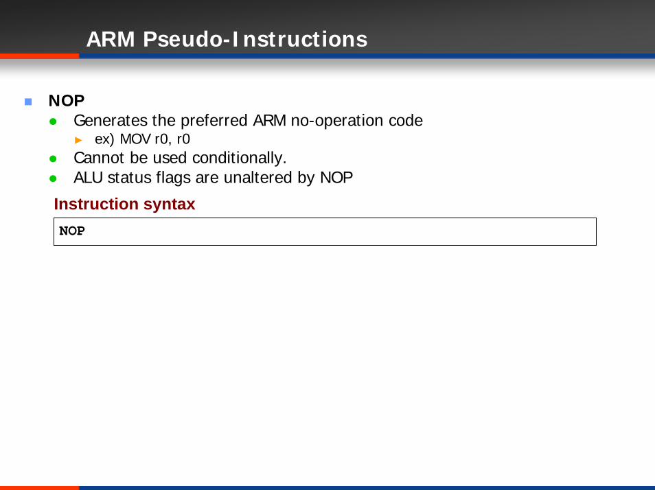
NOPGenerates the preferred ARM no-operation code► ex) MOV r0, r0Cannot be used conditionally.ALU status flags are unaltered by NOP
Instruction syntaxNOP

Directives

ARM Assembly Language Basic
Simple Example
AREA ARMex, CODE, READONLY; Name is ARMex
ENTRY ; Mark first instruction to executestart
MOV r0, #10 ; Set up parameters MOV r1, #3ADD r0, r0, r1 ; r0 = r0+r1
stopMOV r0, #0x18LDR r1, =0x20026 ; Application ExitSWI 0x123456 ; ARM semihosting SWI
END ; Mark end of file

ARM Assembly Language Basic
Line
Case rulescan be upper or lower cases, but not mixed
Line lengthlong line can be split onto several lines by backslash (₩)► but limited by 128 ~ 256
Labelssymbols that represent address► calculated during assembly
Local labels%{F|B}{A|T}nn: 0 ~ 99
Comments;
{label} {instruction|directive|pseudo-instruction} {;comment}

ARM Assembly Language Basic
ConstantsNumbers► Decimal: 123► Hexadecimal: 0x78► n_xxx
n: base between 2 and 9xxx: number in that base
Boolean► {TRUE}, {FALSE}
Characters► ‘a’, ‘b’, …Strings► “abcde 123 $$ xyz”

Directives
AREAinstructs assembler to assemble a new code or data sectionsections are independent indivisible chunks of code or data manipulated by the linker
► CODE, DATA► READONLY, READWRITE
ENTRYentry point for application
ENDinstructs the assembler to stop processing this source file
CODE32/CODE16instructs the assembler to assemble as ARM/Thumb instructions
AREA sectionname{, attr}{,attr} …

Directives
DCB (=), DCW, DCD (&), DCQ, DCIAllocates 1, 2, 4, 8 and integer of memory, respectively
Integer defining an ARM or Thumb instruction
► expr: numeric expression, program-relative expression
Example
{label} DCx expr{, expr}
Data1 DCD 1, 5, 20 ; defines 3 word of 1, 5, 20Hello DCB “hello”, 0Data2 DCD mem06+4 ; defines 1 word of label mem06 + 4MyVal DCI 0xEA000000
Directives
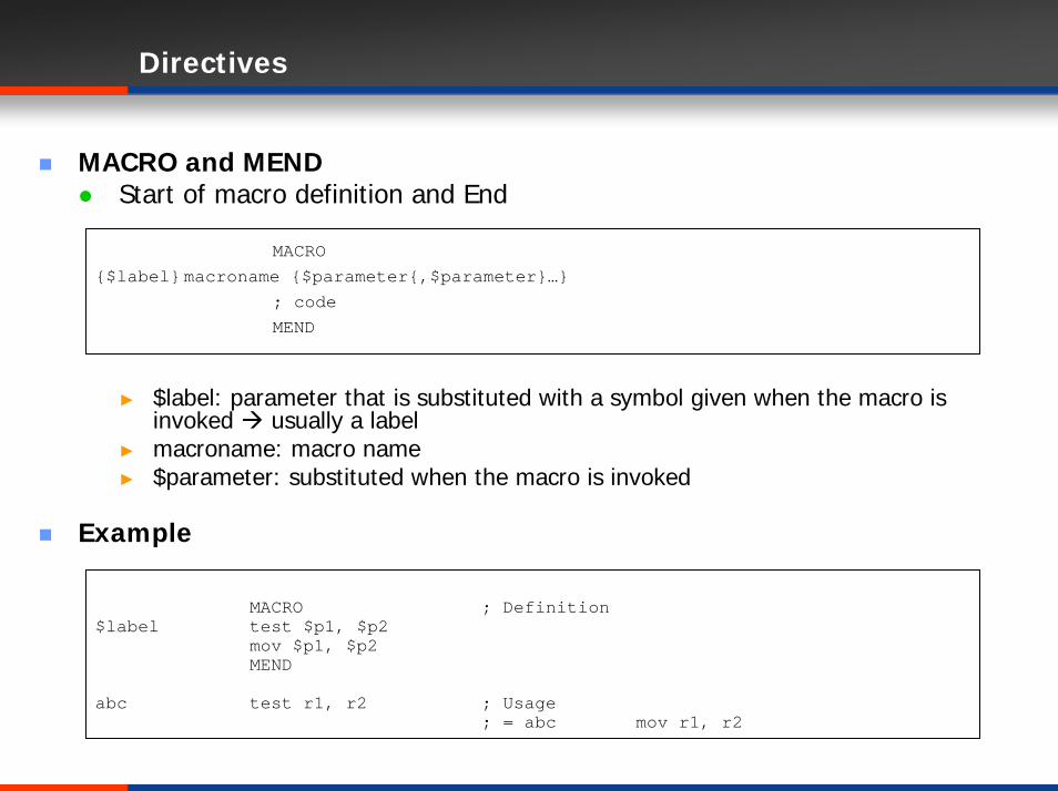
MACRO and MENDStart of macro definition and End
► $label: parameter that is substituted with a symbol given when the macro is invoked usually a label
► macroname: macro name► $parameter: substituted when the macro is invoked
Example
MACRO{$label}macroname {$parameter{,$parameter}…}
; codeMEND
MACRO ; Definition$label test $p1, $p2
mov $p1, $p2MEND
abc test r1, r2 ; Usage; = abc mov r1, r2

Program Example
Calling subroutine
AREA subrout, CODE, READONLY
ENTRYstart MOV r0, #10
MOV r1, #3BL doadd
stop MOV r0, #0x18LDR r1, =0x20026SWI 0x123456
doadd ADD r0, r0, r1MOV pc, lrEND

Program Example
Thumb assembly language
AREA ThumbSub, CODE, READONLY
ENTRYCODE32
header ADR r0, start+1BX r0
CODE16
start MOV r0, #10MOV r1, #3BL doadd
stop MOV r0, #0x18LDR r1, =0x20026SWI 0xAB ; Thumb semihosting SWI
doadd ADD r0, r0, r1MOV pc, lrEND

Questions

ARM
ARM의 RISC 특성으로인한장점을쓰시오
Little endian의 computer friendly 특성에관한예를드시오
ARM register인 SP, LR, PC, CPSR의역할을쓰시오
Exception시참조하는 Vector Table중, FIQ의위치가Table 최하위주소에위치하여얻을수있는장점은?
ARM instruction에서 condition code를가짐으로써얻을수있는이점을쓰시오

ARM
32Bit Machine 상의 h’0000_00A8 의주소에위치한명령어 <BL h’0000_0F24> 가수행되었을때, 다음 PC와LR의값을구하라.
SWI 명령이수행되었을때발생하는 register의변화를설명하시오.
Related Documents
![제09장.ppt [호환 모드] - KOREATECH · 2016. 10. 31. · 미사용상태 미사용상태를가진설계 n F-F은2n이진상태를가짐 이중사용하지않은상태는 don't](https://static.cupdf.com/doc/110x72/60b1ac230cc8a219f71d2eb9/oe09ppt-eeoe-koreatech-2016-10-31-effoe-effoeeee.jpg)


![M06 arith2.ppt [호환 모드] - KOREATECH](https://static.cupdf.com/doc/110x72/625c7a6b52b9094c02225188/m06-koreatech.jpg)