Computer Organization and Components Lecture 5: I/O Systems, part I David Broman Associate Professor, KTH Royal Institute of Technology Assistant Research Engineer, University of California, Berkeley IS1500, fall 2015 Slides version 1.0 Part I Basic I/O and Timers David Broman [email protected] 2 Part II Buses and DMA Course Structure Module 3: Logic Design Module 4: Processor Design Module 1: C and Assembly Programming Module 5: Memory Hierarchy Module 2: I/O Systems Module 6: Parallel Processors and Programs LE1 EX1 LAB1 LE2 LE3 LE4 S1 LAB2 LE5 LE6 EX2 LE7 LE8 EX3 LAB3 LAB4 LE9 LE10 S2 LAB5 LE11 EX4 LAB6 LE12 LE13 EX5 S3 Proj. Expo LE14

Welcome message from author
This document is posted to help you gain knowledge. Please leave a comment to let me know what you think about it! Share it to your friends and learn new things together.
Transcript
Computer Organization and Components
Lecture 5: I/O Systems, part I
David Broman Associate Professor, KTH Royal Institute of Technology
Assistant Research Engineer, University of California, Berkeley
IS1500, fall 2015
Slides version 1.0
Part I Basic I/O and Timers
David Broman [email protected]
2
Part II Buses and DMA
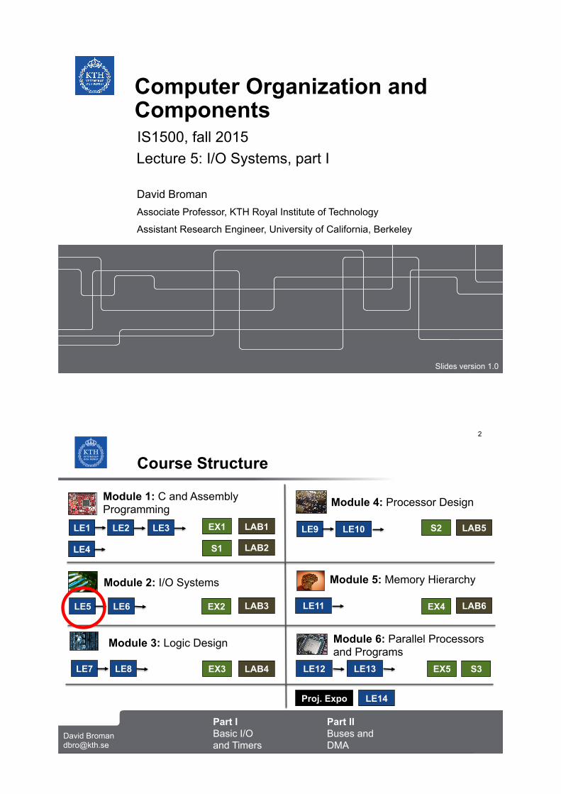
Course Structure
Module 3: Logic Design
Module 4: Processor Design Module 1: C and Assembly Programming
Module 5: Memory Hierarchy Module 2: I/O Systems
Module 6: Parallel Processors and Programs
LE1 EX1 LAB1 LE2 LE3
LE4 S1 LAB2
LE5 LE6 EX2
LE7 LE8 EX3
LAB3
LAB4
LE9 LE10 S2 LAB5
LE11 EX4 LAB6
LE12 LE13 EX5 S3
Proj. Expo LE14
Part I Basic I/O and Timers
David Broman [email protected]
3
Part II Buses and DMA
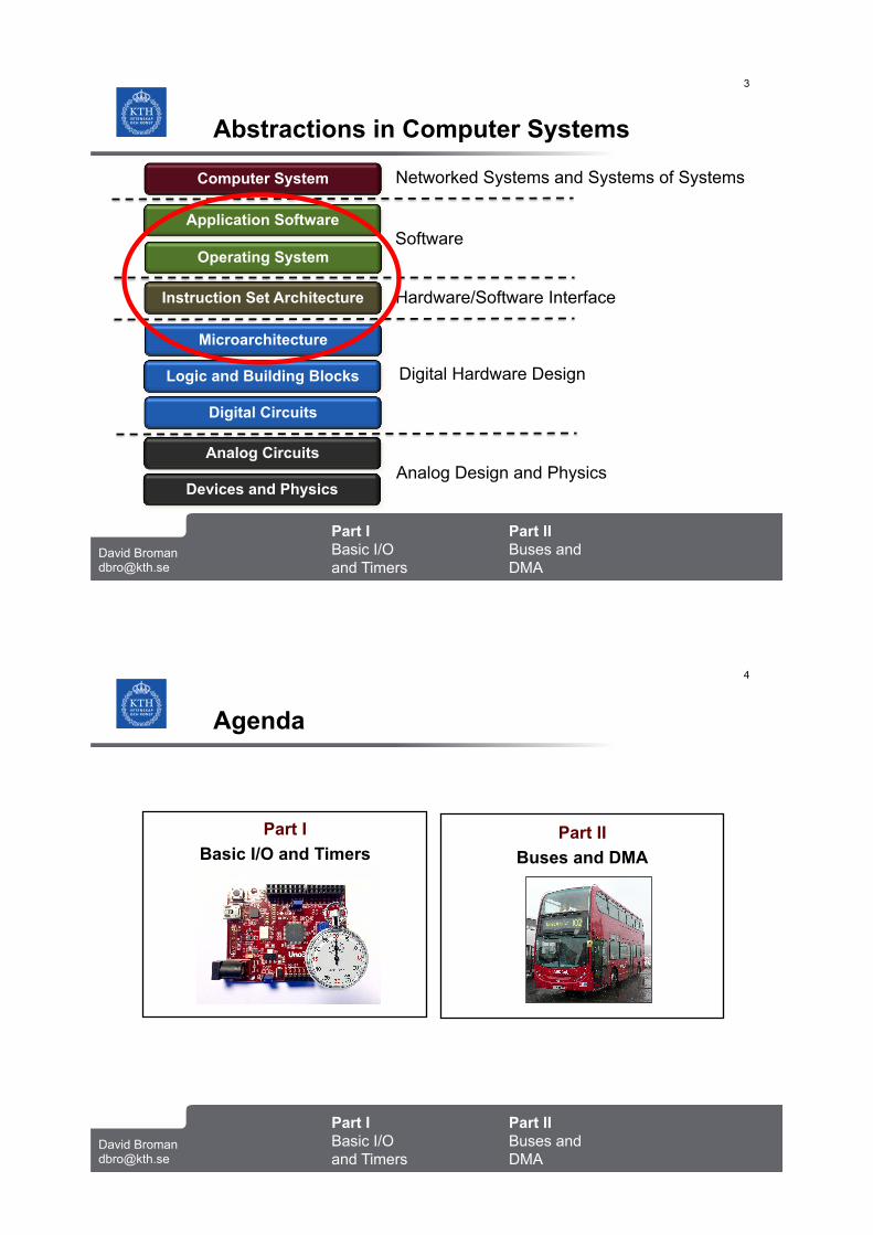
Abstractions in Computer Systems
Instruction Set Architecture
Microarchitecture
Logic and Building Blocks
Digital Circuits
Analog Circuits
Devices and Physics
Operating System
Application Software
Computer System Networked Systems and Systems of Systems
Software
Hardware/Software Interface
Digital Hardware Design
Analog Design and Physics
Part I Basic I/O and Timers
David Broman [email protected]
4
Part II Buses and DMA
Agenda
Part I
Basic I/O and Timers Part II
Buses and DMA

Part I Basic I/O and Timers
David Broman [email protected]
5
Part II Buses and DMA
Part I
Basic I/O and Timers
Acknowledgement: The structure and several of the good examples are derived from the book “Digital Design and Computer Architecture” (2013) by D. M. Harris and S. L. Harris.
Part I Basic I/O and Timers
David Broman [email protected]
6
Part II Buses and DMA
I/O Devices - Examples
Keyboard
Device
Compiler Tool Chains
Processor
Memory
I/O = Input / Output
Source: Patterson & Hennessy, “Computer Organiziation and Design” 4th edition, 2012
Behavior Partner Data Rate (Mbit/sec)
Input Human 0.0001 Mouse Input Human 0.0038 Laser Printer Output Human 3.2000 Graphics Display Output Human 800.0 – 8000.0 Network/LAN Input/Output Machine 100.0 – 10000.0 Flash Memory Storage Machine 32.0 – 200.0
In embedded systems, I/O devices can be, for instance, microwave controller, fuel injector in an engine, motors, etc.
I/O Devices (also called peripherals) for a PC or mobile device.
Part I Basic I/O and Timers
David Broman [email protected]
7
Part II Buses and DMA
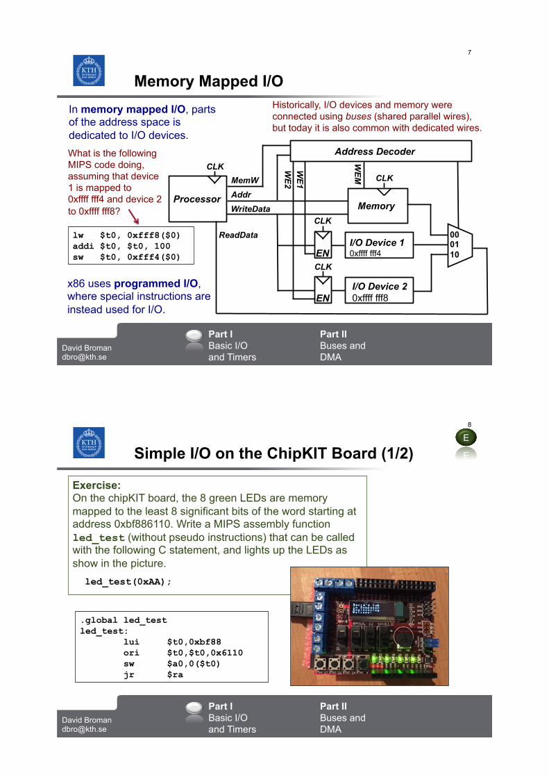
Memory Mapped I/O In memory mapped I/O, parts of the address space is dedicated to I/O devices.
Processor
Address Decoder
Memory
I/O Device 1 0xffff fff4 EN
I/O Device 2 0xffff fff8
EN
00 01 10
CLK
CLK
CLK
CLK MemW Addr WriteData
WE2
WE1
WEM
What is the following MIPS code doing, assuming that device 1 is mapped to 0xffff fff4 and device 2 to 0xffff fff8?
Historically, I/O devices and memory were connected using buses (shared parallel wires), but today it is also common with dedicated wires.
ReadData lw $t0, 0xfff8($0) addi $t0, $t0, 100 sw $t0, 0xfff4($0)
x86 uses programmed I/O, where special instructions are instead used for I/O.
Part I Basic I/O and Timers
David Broman [email protected]
8
Part II Buses and DMA
Simple I/O on the ChipKIT Board (1/2)
Exercise: On the chipKIT board, the 8 green LEDs are memory mapped to the least 8 significant bits of the word starting at address 0xbf886110. Write a MIPS assembly function led_test (without pseudo instructions) that can be called with the following C statement, and lights up the LEDs as show in the picture.
led_test(0xAA);
.global led_test led_test: lui $t0,0xbf88 ori $t0,$t0,0x6110 sw $a0,0($t0) jr $ra
E
Part I Basic I/O and Timers
David Broman [email protected]
9
Part II Buses and DMA
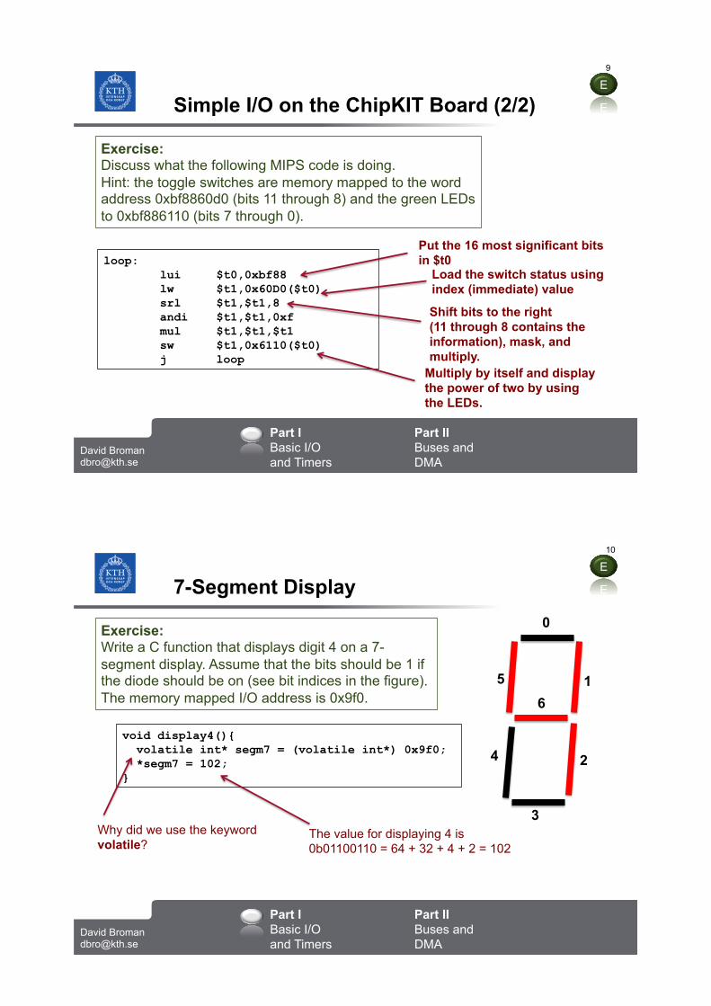
Simple I/O on the ChipKIT Board (2/2)
Exercise: Discuss what the following MIPS code is doing. Hint: the toggle switches are memory mapped to the word address 0xbf8860d0 (bits 11 through 8) and the green LEDs to 0xbf886110 (bits 7 through 0).
loop: lui $t0,0xbf88 lw $t1,0x60D0($t0) srl $t1,$t1,8 andi $t1,$t1,0xf mul $t1,$t1,$t1 sw $t1,0x6110($t0) j loop
Put the 16 most significant bits in $t0
Shift bits to the right (11 through 8 contains the information), mask, and multiply.
E
Load the switch status using index (immediate) value
Multiply by itself and display the power of two by using the LEDs.
Part I Basic I/O and Timers
David Broman [email protected]
10
Part II Buses and DMA
7-Segment Display
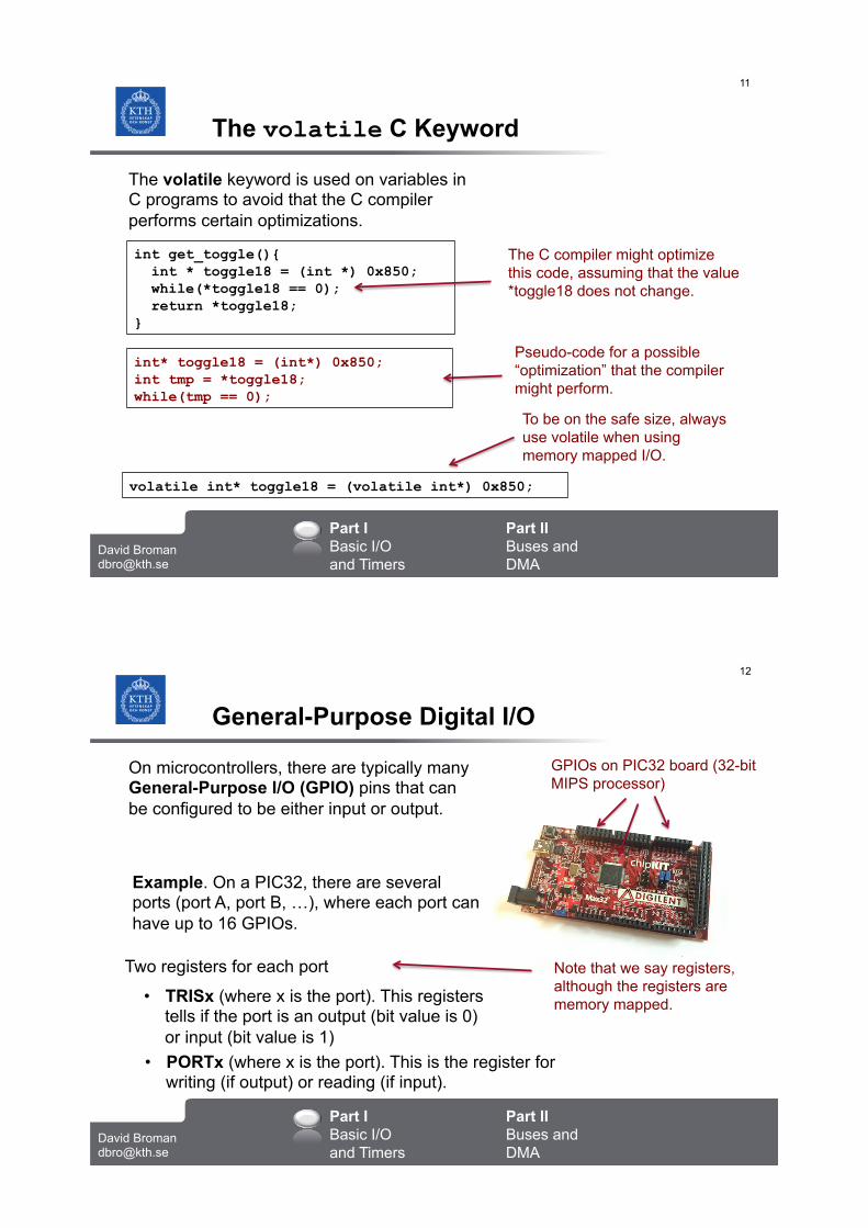
Exercise: Write a C function that displays digit 4 on a 7-segment display. Assume that the bits should be 1 if the diode should be on (see bit indices in the figure). The memory mapped I/O address is 0x9f0.
E
0
1
2
3
4
5 6
void display4(){ volatile int* segm7 = (volatile int*) 0x9f0; *segm7 = 102; }
The value for displaying 4 is 0b01100110 = 64 + 32 + 4 + 2 = 102
Why did we use the keyword volatile?
Part I Basic I/O and Timers
David Broman [email protected]
11
Part II Buses and DMA
The volatile C Keyword
int get_toggle(){ int * toggle18 = (int *) 0x850; while(*toggle18 == 0); return *toggle18; }
The C compiler might optimize this code, assuming that the value *toggle18 does not change.
The volatile keyword is used on variables in C programs to avoid that the C compiler performs certain optimizations.
volatile int* toggle18 = (volatile int*) 0x850;
int* toggle18 = (int*) 0x850; int tmp = *toggle18; while(tmp == 0);
Pseudo-code for a possible “optimization” that the compiler might perform.
To be on the safe size, always use volatile when using memory mapped I/O.
Part I Basic I/O and Timers
David Broman [email protected]
12
Part II Buses and DMA
General-Purpose Digital I/O
On microcontrollers, there are typically many General-Purpose I/O (GPIO) pins that can be configured to be either input or output.
GPIOs on PIC32 board (32-bit MIPS processor)
Example. On a PIC32, there are several ports (port A, port B, …), where each port can have up to 16 GPIOs.
Two registers for each port
• TRISx (where x is the port). This registers tells if the port is an output (bit value is 0) or input (bit value is 1)
• PORTx (where x is the port). This is the register for writing (if output) or reading (if input).
Note that we say registers, although the registers are memory mapped.
Part I Basic I/O and Timers
David Broman [email protected]
13
Part II Buses and DMA
GPIO and Basic I/O for chipKIT boards
43 GPIO pins. GPIO pins are connected when the shield is attached to the Uno32 board. These pins are also connected to other components on the I/O shield.
4 push buttons
8 LEDs
4 switches
Basic IO shield. Uno32
Part I Basic I/O and Timers
David Broman [email protected]
14
Part II Buses and DMA
General-Purpose Digital I/O Information
Links on the course webpage under “Literature and Resources”
How can we find out how to use the different ports?
Answer: Reference manuals, data sheets, and header files.
Example: which port and bit should be used for reading the status of push button number 1?
Part I Basic I/O and Timers
David Broman [email protected]
15
Part II Buses and DMA
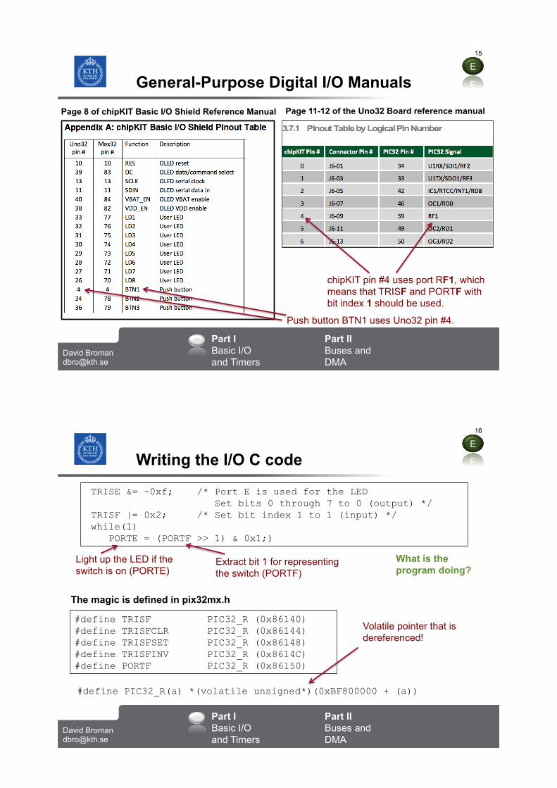
General-Purpose Digital I/O Manuals Page 11-12 of the Uno32 Board reference manual Page 8 of chipKIT Basic I/O Shield Reference Manual
Push button BTN1 uses Uno32 pin #4.
chipKIT pin #4 uses port RF1, which means that TRISF and PORTF with bit index 1 should be used.
E
Part I Basic I/O and Timers
David Broman [email protected]
16
Part II Buses and DMA
Writing the I/O C code
The magic is defined in pix32mx.h
#define TRISF PIC32_R (0x86140) #define TRISFCLR PIC32_R (0x86144) #define TRISFSET PIC32_R (0x86148) #define TRISFINV PIC32_R (0x8614C) #define PORTF PIC32_R (0x86150)
TRISE &= ~0xf; /* Port E is used for the LED Set bits 0 through 7 to 0 (output) */ TRISF |= 0x2; /* Set bit index 1 to 1 (input) */ while(1) PORTE = (PORTF >> 1) & 0x1;)
What is the program doing?
Extract bit 1 for representing the switch (PORTF)
Light up the LED if the switch is on (PORTE)
#define PIC32_R(a) *(volatile unsigned*)(0xBF800000 + (a))
Volatile pointer that is dereferenced!
E

Part I Basic I/O and Timers
David Broman [email protected]
17
Part II Buses and DMA
Timers Timers are I/O devices that are used to measure time.
A timer is driven by a clock source. Either internal (synchronous with processor clock) or external (asynchronous).
Period Register
Control Register(s)
Clock Source
Timer Value
Timers can be configured in different ways, but have basically the following components.
Example, 50Mhz external clock.
Can use prescaling k:1. It counts every k tick. For instance 256:1
• Tells if time-out is reached.
• Stop/start counting • Check if running.
Write registers, saying the start number when counting (or final, depending if counting up or down)
Read register. A “snap-shot” of the timer value.
Part I Basic I/O and Timers
David Broman [email protected]
18
Part II Buses and DMA
Part II
Buses and DMA
Part I Basic I/O and Timers
David Broman [email protected]
19
Part II Buses and DMA
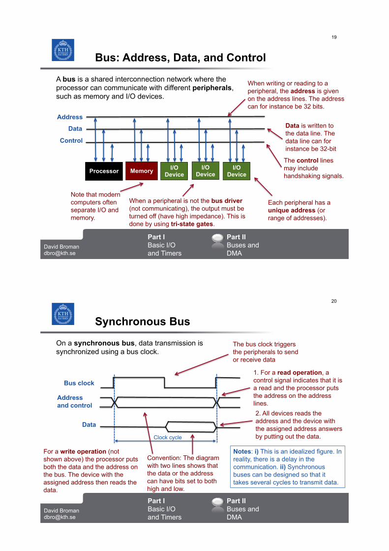
Bus: Address, Data, and Control
Address
Each peripheral has a unique address (or range of addresses).
Data
Control
A bus is a shared interconnection network where the processor can communicate with different peripherals, such as memory and I/O devices.
I/O Device
Memory
Processor
I/O Device
I/O Device
When writing or reading to a peripheral, the address is given on the address lines. The address can for instance be 32 bits.
Data is written to the data line. The data line can for instance be 32-bit
The control lines may include handshaking signals.
Note that modern computers often separate I/O and memory.
When a peripheral is not the bus driver (not communicating), the output must be turned off (have high impedance). This is done by using tri-state gates.
Part I Basic I/O and Timers
David Broman [email protected]
20
Part II Buses and DMA
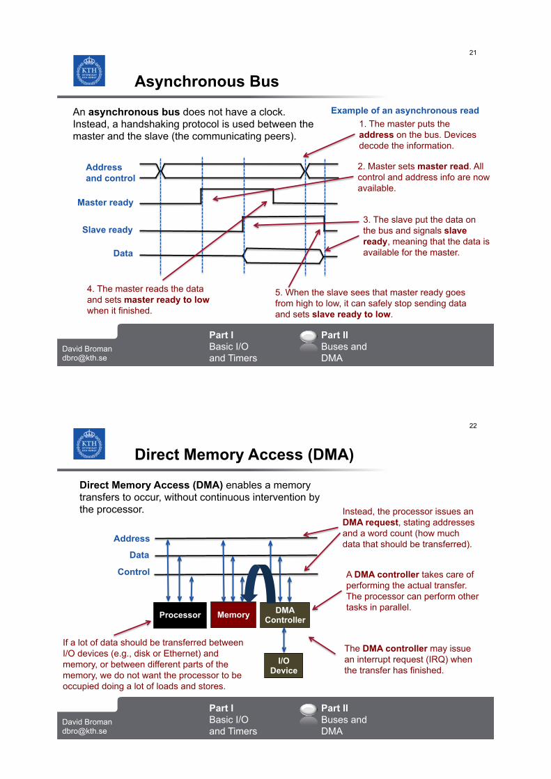
Synchronous Bus
Bus clock
The bus clock triggers the peripherals to send or receive data
Address and control
Data
On a synchronous bus, data transmission is synchronized using a bus clock.
Clock cycle
Convention: The diagram with two lines shows that the data or the address can have bits set to both high and low.
1. For a read operation, a control signal indicates that it is a read and the processor puts the address on the address lines. 2. All devices reads the address and the device with the assigned address answers by putting out the data.
For a write operation (not shown above) the processor puts both the data and the address on the bus. The device with the assigned address then reads the data.
Notes: i) This is an idealized figure. In reality, there is a delay in the communication. ii) Synchronous buses can be designed so that it takes several cycles to transmit data.
Part I Basic I/O and Timers
David Broman [email protected]
21
Part II Buses and DMA
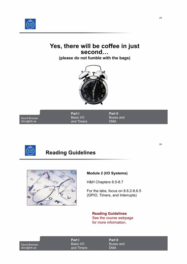
Asynchronous Bus
Master ready
Example of an asynchronous read
Address and control
Data
An asynchronous bus does not have a clock. Instead, a handshaking protocol is used between the master and the slave (the communicating peers).
Slave ready
1. The master puts the address on the bus. Devices decode the information.
2. Master sets master read. All control and address info are now available.
3. The slave put the data on the bus and signals slave ready, meaning that the data is available for the master.
4. The master reads the data and sets master ready to low when it finished.
5. When the slave sees that master ready goes from high to low, it can safely stop sending data and sets slave ready to low.
Part I Basic I/O and Timers
David Broman [email protected]
22
Part II Buses and DMA
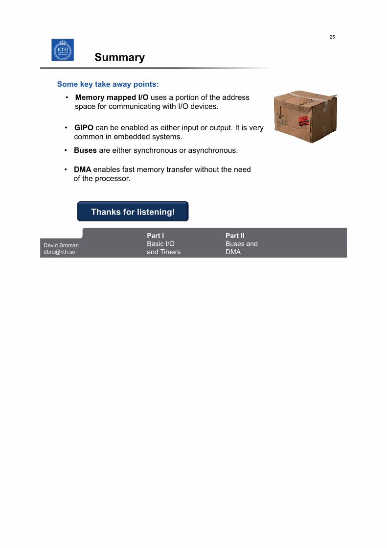
Direct Memory Access (DMA)
Address
Data
Control
Direct Memory Access (DMA) enables a memory transfers to occur, without continuous intervention by the processor.
DMA Controller
Memory
Processor
I/O Device
If a lot of data should be transferred between I/O devices (e.g., disk or Ethernet) and memory, or between different parts of the memory, we do not want the processor to be occupied doing a lot of loads and stores.
Instead, the processor issues an DMA request, stating addresses and a word count (how much data that should be transferred).
A DMA controller takes care of performing the actual transfer. The processor can perform other tasks in parallel.
The DMA controller may issue an interrupt request (IRQ) when the transfer has finished.
Part I Basic I/O and Timers
David Broman [email protected]
23
Part II Buses and DMA
Yes, there will be coffee in just
second… (please do not fumble with the bags)
Part I Basic I/O and Timers
David Broman [email protected]
24
Part II Buses and DMA
Reading Guidelines
Module 2 (I/O Systems) H&H Chapters 8.5-8.7 For the labs, focus on 8.6.2-8.6.5 (GPIO, Timers, and Interrupts)
Reading Guidelines See the course webpage for more information.
Part I Basic I/O and Timers
David Broman [email protected]
25
Part II Buses and DMA
Summary
Thanks for listening!
Some key take away points: • Memory mapped I/O uses a portion of the address
space for communicating with I/O devices.
• GIPO can be enabled as either input or output. It is very common in embedded systems.
• Buses are either synchronous or asynchronous.
• DMA enables fast memory transfer without the need of the processor.
Related Documents