Computer Organization and Architecture Introduction

Computer Organization and Architecture Introduction.
Dec 24, 2015
Welcome message from author
This document is posted to help you gain knowledge. Please leave a comment to let me know what you think about it! Share it to your friends and learn new things together.
Transcript

Computer Organization and Architecture
Introduction

Architecture & Organization 1
Architecture is those attributes visible to the programmer Instruction set, number of bits used for data
representation, I/O mechanisms, addressing techniques.
e.g. Is there a multiply instruction?Organization is how features are
implemented, typically hidden from the programmer Control signals, interfaces, memory technology. e.g. Is there a hardware multiply unit or is it
done by repeated addition?

Architecture & Organization 2
All Intel x86 family share the same basic architecture
The IBM System/370 family share the same basic architecture
This gives code compatibility At least backwards But… increases complexity of each new generation.
May be more efficient to start over with a new technology, e.g. RISC vs. CISC
Organization differs between different versions

Levels of Machines
Computers are complex; easier to understand if broken up into hierarchical components.

Structure & Function
At each level the designer should consider Structure : the way in which components
relate to each other Function : the operation of individual
components as part of the structure
Let’s look at the computer hardware top-down starting with function. Later we’ll look at software

Function
All computer functions are: Data processing Data storage Data movement Control

Functional view
Functional view of a computer
DataMovementApparatus
ControlMechanism
DataStorageFacility
DataProcessingFacility

Operations (1)
Data movement e.g. keyboard to screen
DataMovementApparatus
ControlMechanism
DataStorageFacility
DataProcessingFacility

Operations (2)
Storage e.g. Internet download to disk
DataMovementApparatus
ControlMechanism
DataStorageFacility
DataProcessingFacility

Operation (3)
Processing from/to storage e.g. updating bank statement
DataMovementApparatus
ControlMechanism
DataStorageFacility
DataProcessingFacility

Operation (4)
Processing from storage to I/O e.g. printing a bank statement
DataMovementApparatus
ControlMechanism
DataStorageFacility
DataProcessingFacility

Structure
Major Components of a Computer Central Processing Unit (CPU) – Controls the
operation of the computer and performs data processing
Main Memory – Stores data Input Output (I/O) – Moves data between the
computer and the external environment System Interconnect – Some mechanism that
provides for communications between the system components, typically a bus (set of wires)

Structure - Top Level
Computer
Main Memory
InputOutput
SystemsInterconnection
Peripherals
Communicationlines
CentralProcessing Unit
Computer

Generic System Bus
System Bus = Data, Address, and Control Bus (set of wires, e.g. 32 wires each)Typically multiple I/O buses, power bus, etc.

Structure - CPU
Major components of the CPU Control Unit (CU) – Controls the operation of the
CPU Arithmetic and Logic Unit (ALU) – Performs data
processing functions, e.g. arithmetic operations Registers – Fast storage internal to the CPU, but
contents can be copied to/from main memory CPU Interconnect – Some mechanism that
provides for communication among the control unit, ALU, and registers
Structure - The CPU
Computer Arithmeticand Login Unit
ControlUnit
Internal CPUInterconnection
Registers
CPU
I/O
Memory
SystemBus
CPU

Structure – Inside the CPU
The implementation of registers and the ALU we will leave primarily to EE 241
We will say a bit about the architecture of the control unit, there are many possible approaches. A common approach is the microprogrammed
control unit, where the control unit is in essence itself a miniature computer, where a CPU instruction is implemented via one or more “micro instructions”
Sequencing Logic – Controlling the order of eventsMicroprogram Control Unit – Internal controlsMicroprogram Registers, Memory

Structure – A Microprogrammed Control Unit
CPU
ControlMemory
Control Unit Registers and Decoders
SequencingLogin
ControlUnit
ALU
Registers
InternalBus
Control Unit

Computer Evolution and Performance
Better, Faster, Cheaper?

History: ENIAC background
Electronic Numerical Integrator And Computer
Eckert and MauchlyUniversity of PennsylvaniaTrajectory tables for weapons, BRLStarted 1943Finished 1946
Too late for war effort
Used until 1955

ENIAC - details
Decimal (not binary)20 accumulators of 10 digits (ring of 10 tubes)Programmed manually by switches18,000 vacuum tubes30 tons15,000 square feet140 kW power consumption (about $10/hr
today)5,000 additions per second

Vacuum Tubes
Grid regulates flow from of electrons from the cathode


von Neumann/Turing
ENIAC : Very tedious to manually wire programsvon Neumann architecture:
Stored Program concept Main memory storing programs and data ALU operating on binary data Control unit interpreting instructions from memory
and executing Input and output equipment operated by control unit Princeton Institute for Advanced Studies
IAS Completed 1952

Structure of von Neumann machine
MainMemory
Arithmetic and Logic Unit
Program Control Unit
InputOutputEquipment

IAS - details
1000 x 40 bit words Binary number 2 x 20 bit instructions
Set of registers (storage in CPU) Memory Buffer Register Memory Address Register Instruction Register Instruction Buffer Register Program Counter Accumulator Multiplier Quotient
0 1 39
Sign bit
Number Word
Instruction Word
0 8 20 28 39
LeftOpCode Address
RightOpCode Address

Structure of IAS - detail
MainMemory
Arithmetic and Logic Unit
Program Control Unit
InputOutputEquipment
MBR
Arithmetic & Logic Circuits
MQAccumulator
MAR
ControlCircuits
IBR
IR
PC
Address
Instructions& Data
Central Processing Unit

IAS Instruction Cycle
The IAS repetitively performs the instruction cycle: Fetch
Opcode of the next instruction is loaded into the IR Address portion is loaded into the MAR Instruction either taken from the IBR or obtained from memory
by loading the PC into the MAR, memory to the MBR, then the MBR to the IBR and the IR
• To simplify electronics, only one data path from MBR to IR Execute
Circuitry interprets the opcode and executes the instruction Moving data, performing an operation in the ALU, etc.
IAS had 21 instructions Data transfer, Unconditional branch, conditional branch,
arithmetic, address modification

Commercial Computers
1947 - Eckert-Mauchly Computer Corporation
UNIVAC I (Universal Automatic Computer)US Bureau of Census 1950 calculationsBecame part of Sperry-Rand CorporationLate 1950s - UNIVAC II
Faster More memory Upward compatible with older machines

IBM
Punched-card processing equipment1953 - the 701
IBM’s first stored program computer Scientific calculations
1955 - the 702 Business applications
Lead to 700/7000 series

Transistors
Replaced vacuum tubesSmallerCheaperLess heat dissipationSolid State deviceMade from Silicon (Sand)Invented 1947 at Bell LabsShockley, Brittain, Bardeen

Transistor Based Computers
Second generation of machinesNCR & RCA produced small transistor
machinesIBM 7000DEC - 1957
Produced PDP-1

IBM 7094
Last member of the 7000 series 50 times faster than the 701
1.4 uS vs. 30 uS cycle 32K memory vs. 2K Main memory: Core memory vs. Tubes CPU memory: transistors vs. Tubes 185 vs. 24 opcodes Instruction fetch overlap, reduced another trip
to memory (exception are branches) Data channels, independent I/O module for
devices

3rd Generation: Integrated Circuits
Self-contained transistor is a discrete component Big, manufactured separately, expensive, hot
when you have thousands of them
Integrated Circuits Transistors “etched” into a substrate, bundled
together instead of discrete components Allowed thousands of transistors to be
packaged together efficiently

Microelectronics
Literally - “small electronics”A computer is made up of gates, memory
cells and interconnectionsThese can be manufactured on a
semiconductor, e.g. silicon wafer Thin wafer divided into chips Each chip consists of many gates/memory cells Chip packaged together with pins, assembled
on a printed circuit board

Generations of Computer
Vacuum tube - 1946-1957 Transistor - 1958-1964 Small scale integration - 1965 on
Up to 100 devices on a chip Medium scale integration - to 1971
100-3,000 devices on a chip Large scale integration - 1971-1977
3,000 - 100,000 devices on a chip Very large scale integration - 1978 to date
100,000 - 100,000,000 devices on a chip Pentium IV has about 40 million transistors
Ultra large scale integration Over 100,000,000 devices on a chip (vague term)

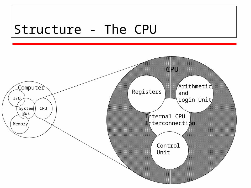
Moore’s Law
Increased density of components on chip Gordon Moore : co-founder of Intel Number of transistors on a chip will double every year Since 1970’s development has slowed a little
Number of transistors doubles every 18 months Cost of a chip has remained almost unchanged Higher packing density means shorter electrical paths,
giving higher performance Smaller size gives increased flexibility Reduced power and cooling requirements Fewer interconnections increases reliability Intel 8/13/02: Announced 0.09 micron process
Human hair ~70 microns
Growth in CPU Transistor Count

IBM 360 series
1964 Replaced (& not compatible with) 7000 series
Reason: Needed to break out of constraints of the 7000 architecture
First planned “family” of computers Similar or identical instruction sets Similar or identical O/S Increasing speed Increasing number of I/O ports (i.e. more terminals) Increased memory size Increased cost (not always the case today!)
Multiplexed switch structure

DEC PDP-8
1964First minicomputer (after miniskirt!)Did not need air conditioned roomSmall enough to sit on a lab bench$16,000
$100k+ for IBM 360
Embedded applications & OEMBUS STRUCTURE

DEC - PDP-8 Bus Structure
OMNIBUS
ConsoleController
CPU Main Memory I/OModule
I/OModule
96 separate signal paths to carry control, address, data signalsHighly flexible, allowed modules to be plugged in for different configurations

Other Innovations - Semiconductor Memory
1970FairchildSize of a single core
i.e. 1 bit of magnetic core storage Held 256 bits
Non-destructive readMuch faster than coreCapacity approximately doubles each year

Intel
1971 - 4004 First microprocessor All CPU components on a single chip 4 bit
Followed in 1972 by 8008 8 bit Both designed for specific applications
1974 - 8080 Intel’s first general purpose microprocessor
Evolution: 8086, 8088, 80286, 80386, 80486, Pentium Pentium Pro, Pentium II, Pentium III, Pentium IV, Itanium

Speeding it up
Smaller manufacturing process (0.09 micron)PipeliningOn board cacheOn board L1 & L2 cacheBranch predictionData flow analysisSpeculative executionParallel execution

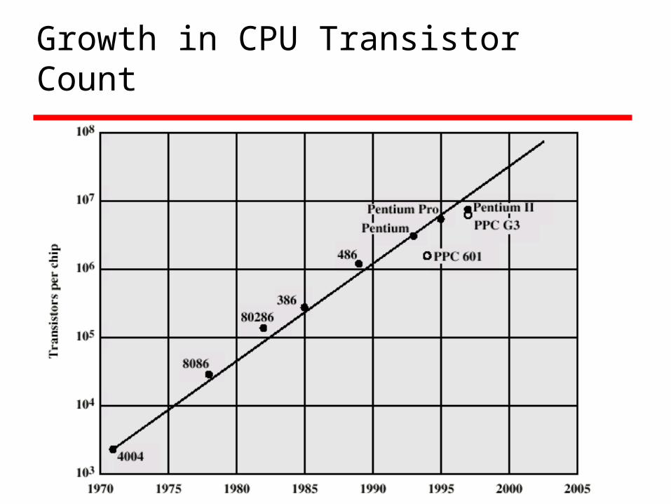
Performance Mismatch
Processor speed increasedMemory capacity increasedMemory speed lags behind processor
speed
Common memory chip technology DRAM = Dynamic Random Access Memory

DRAM and Processor Characteristics

Trends in DRAM use
Solutions
Increase number of bits retrieved at one time Make DRAM “wider” rather than “deeper”
Change DRAM interface Cache
Reduce frequency of memory access More complex cache and cache on chip
Increase interconnection bandwidth High speed buses Hierarchy of buses
Similar problems with I/O devices, e.g. graphics, network Need balance in computer design
Related Documents