1 Computer Engineering 440 Digital Design: II Course Lecture Notes Summer 2002 © W.D. Little Dept. of Electrical and Computer Engineering University of Victoria

Welcome message from author
This document is posted to help you gain knowledge. Please leave a comment to let me know what you think about it! Share it to your friends and learn new things together.
Transcript

1
Computer Engineering 440
Digital Design: II
Course Lecture NotesSummer 2002
©W.D. Little
Dept. of Electrical and ComputerEngineering
University of Victoria

2
Preface
These lecture notes complement the material covered in thetextbook and the lab book for the course. The material covered is afollow on from the material covered in CENG 290. The textbook forthe course is Contemporary Logic Design by Randy H. Katz,Benjamin/Cummings, 1994.

3
CENG 440 Lecture Topics
ArithmeticAddition
Ripple AddersCarry Lookahead AddersCarry Select AddersCarry Save Adders
SubtractionMultiplication
Unsigned Array Multiplication2s Complement MultiplicationLong Multiplication
DivisionRestoring DivisionNonrestoring Division
Logic AnalyzerBlock diagramSoftwareSamplingClockingTriggeringDisplay
XILINX FPGAsXC2064 Logic Cell Array StructureXC2064 I/O Block StructureXC2064 Configurable Logic Block StructureConfiguration Memory CellFlip Flop ImplementationLogic Function GenerationGeneral Purpose InterconnectDirect InterconnectMiscellaneous FeaturesXC4000
Rewiew of CENG 290Mixed Mode LogicWired-AND and Wired-ORCMOS Transmission Gates

4
Flip-FlopsData Transfer
Finite State Machine DesignSimple Design ExampleSummary of Moore and Mealy Sequential CircuitsNumbers of States, Transitions and Outputs in FSMsAlgorithmic State Machine (ASM) NotationAnalysis of FSMsFSM Design Examples
A Finite String RecognizerTraffic Light ControllerDigital Combination Lock

5
Finite State Machine OptimizationState Minimization
Row-matching MethodImplication Chart Method
State AssignmentFlip-Flop ChoiceFinite State Machine Partitioning
Finite State Machine ImplementationVHDLTraffic Light Controller Implementation
Computer OrganizationRegister Transfer NotationDatapath OrganizationsMealy and Moore Implementations of ControllerCounter Implementation of ControllerROM Based Controllers

6
• Arithmetic
Many digital systems must perform arithmetic. Depending uponsystem requirements the following characteristics must be tradedoff
1. speed2. cost3. precision4. range5. standardization
Almost all digital arithmetic is now performed on data in unsignedbinary format, twos complement format or IEEE floating pointformat. In the following pages we will look at some basic unsignedbinary and twos complement arithmetic techniques for addition,subtraction, multiplication and division. Floating point arithmeticwill not be examined directly, however, the methods we do look atare used within floating point arithmetic systems.
Addition
Unsigned binary arithmetic and twos complement arithmetic use thesame algorithms and hardware except that sign detection andoverflow detection are different. For exampleoverflow = ab/c + /a/bc when twos complement numbers with signbits a and b are added to form a sum with sign bit c. When unsignedbinary numbers are added, overflow is given by the carry out.
Ripple Adders
Simple cascaded full adders. Carry propagation determinesaddition speed.
Carry Lookahead Adders
Bits to be added are handled in groups (eg 4) and carrylookahead generators generate carry_generated signals, G, andcarry_propagate signals, P, to reduce the time for carries topropagate through a group. Carry lookahead adders for long addersare usually arranged in a tree structure to propagate carries quickly

7
across the whole structure. The size of a carry lookahead group islimited by the fan-in of the gates used to generate the carry,propagate and generate signals. Most fast adders use the carrylookahead method.
Carry Select Adders
A carry select adder uses two adders for each group of bits.One of the adders assumes the carry coming into the group is a 0and the other assumes the incoming carry is a 1. Logic is used toselect the sum bits from one of the adders as soon as it is knowwhich of the two assumed carry inputs is the correct carry in forthe group. The figure below shows a simple 8-bit carry select adderwhere two 4-bit adders are used for the high order bits of the adder.
4-bit adder
4-bit adder
4-bit adder
1 0 1 01 01 0
0
1
Cin
S7 S6 S5 S4 S3 S2 S1 S0
C4
CT
CB
C8
C8 = CT/C4 + CBC4This can be simplifiedby noting that if CB=0,CT cannot be 1.Note that the above 8-bit adder can be used to implement a 16-bitcarry select adder and this procedure may be used to build a 2n bitadder.
Note also that the 8-bit adder can be built to have 4 gate delays anda 2n bit adder will have 2n -2 gate delays.

8

9
Carry Save Adders
A CSA is used to add several values without suffering the delay ofseveral adders. A CSA adder is simply an ordered set of unconnectedfull-adder modules. Each CSA adder adds 3 values using the 3 inputsof a full adder as the inputs for 3 corresponding bits of the values.The carry outs of the full adders are connected one position to theleft and added at a lower level.
The figure below shows a 4-bit CSA and a tree of CSAs used to add 68-bit values A,B,C,D,E,F. The kinks in the carry lines of the treeindicate the lines are connected one place to the left. Note thatlonger CSAs are required near the bottom of the tree. One regularadder is also required at the bottom of the tree. Only 2 gate delaysare required for signals to propagate through a CSA.

10
CSA
CSA
CSA
CSA
adder
A B C D E F
Cout
Cin
SUM
8-bit 8-bit
9-bit
10-bit
11-bit
CSA Tree Structure
FA3 FA2 FA1 FA0
a3 b3 c3 a2 b2 c2 a1 a0b1 b0c1 c0
cout3 cout2 cout1 cout0s0s1s2s3
Example 4-bit CSA

11
Subtraction
Subtraction is almost always carried out by addition of the twoscomplement. This in turn is done by adding the logical complementwith an input carry of 1. It is also possible, of course, to use half andfull subtractor modules in the same way that half and full addermodules are used to perform addition.
Multiplication
Unsigned parallel/serial multiplication
For P = M x B where
P = {p15p14...p1p0}, A = {m7m6...m1m0}, B ={b7b6...b1b0}
a simple form of the parallel/serial algorithm is as follows.
P = 0For i =0 to 7
P = P + mi x B x 28P = P/2
Endfor
A suitable datapath for this procedure is as follows
8-bit adder
8-bit B register
mi
8-bit Pl register9-bit Ph register
load9 shift17

12
Initially the 9 most significant bits of the P register, Ph, are cleared,and the multiplier, M, is loaded into the 8 least significant bits Pl.The multiplicand, B, is loaded into the B register. On each cycle thecontroller loads 9 bits from the adder if mi = 1 and then shifts the17 bit P register right 1 bit. After 8 cycles, the 16 bit product isavailable as the 16 least significant bits of the P register. Note thatthe load and shift could be combined. This would save cycles andeliminate the need for a 17th bit in the P register.
Unsigned Array Multiplication
The serial operations carried out by the parallel/serial multipliercan be done by the following array multiplier.

13
a7 a6 a0
a7 a6 a0
a7 a6 a0
0 00
m0
m1
m7
p0p1p7p14p15
adder
adder
adder
The implementation given above would be rather slow because ofthe long propagation times through the adders. This propagationtime can be greatly reduced by using carry save adders for alladders but the bottom adder. When this is done the entire multiplierexcept the final adder can be implemented with the following gatedCSA modules.

14
FAa b c
scout
2s Complement Multiplication
An algorithm developed by A.D. Booth (now retired and living inSooke) is commonly used for multiplication of 2s complementnumbers.
Consider P = M x A where M and A are both 8 bit 2s complementnumbers.
6M = -m7 27 + Σ mi 2i for a 2s complement number.
i=0
If we define m-1 = 0 then we can write
7M = Σ (mi-1 -mi) 2i
i=0
This tells us that we can perform 2s complement multiplication inmuch the same manner as unsigned multiplication if we
add_multiplicand = mi-1/mi
sub_multiplicand = /mi-1mi
add_zero = (mi-1=mi)

15
Long Multiplication
Multiplication of long numbers can be performed by multipleparallel or serial multiplications. Consider the multiplication of two16 numbers treated as 8-bit components
P = (28a + b)(28c + d)
= 216ac + 28(ad + bc) + bd
The component multiplications can be arranged for addition asillustrated below.
---------------- bd ---------------- ad ---------------- bc
---------------- ac _____________________________ ---------------------------------- P
The 8 least significant bits of bd are the 8 least significant bits of theproduct. Two 8-bit CSAs can be used to add the three 8-bit numbersthat form the middle 16 bits of the product. An 8-bit adder formsthe 8 most significant bits of the 32-bit product.
The above approach can be used to implement multipliers fornumbers of length 2n . Note that a 1-bit multiplier is an AND gate!
Division
There are two classical algorithms for performing division ofunsigned binary numbers; restoring division and non-restoringdivision. Modern high-speed division algorithms use an iterativeapproach that depends upon fast multiplication.
Division algorithms determine an n bit quotient, Q, and an n bitremainder, R, corresponding to an n bit numerator, N, and an n bitdenominator, D. We assume that N,D,Q and R are all integers.Therefore
N/D = Q + R/D

16
The restoring and nonrestoring algorithms follow from manual longdivision. Consider the following decimal and binary examples
1 7 1 2 3 4 51 1 9
4 43 41 0 51 0 2
3
0 0 7 2 6
101 1 1 0 1 0 0 1 1
0 0 1 0 1 0 1 0
1 0 1
1 1 01 0 1
1 0 11 0 1
0 0 0 1In these examples it is seen that we first determine how many timesD goes into the most significant digit of N. The number of times itgoes is the value of the most significant digit of Q. The remainderafter the first cycle is then concatenated with the next digit of N andthe process is repeated to get all quotient digits and the finalremainder.
Restoring Division
For 8-bit binary numbers, we can use a 16 bit X register and performarithmetic on the most significant 8 bits of X that we will call Xh.The algorithm is as follows
X = NFor i = 7 to 0
X = 2XX = X - 28DIf Xh >= 0 then qi = 1
else qi = 0X = X + 28D
Endfor
This algorithm determines the quotient bits q7....q0 and theremainder R which is the final value of Xh. If qi in the algorithm isreplaced by X0, the final value of X will contain R in the high byteand Q in the low byte. Note also that if we add the 2s complement ofD to subtract D from Xh, a carry out of the addition will indicatethat Xh >=0.

17
Nonrestoring Division
Note that if Xh is <0 in the restoring algorithm, the following 3operations are performed on X before the next If statement
X = X + 28DX = 2XX = X - 28D
These are equivalent to X = 2(X + 28D) - 28D = 2X + 28D.That is, rather than restore X to a positive value , we can simply shiftand add D when the previous bit is 0. The nonrestoring algorithm istherefore
q8 = 1X = NFor i = 7 to 0
X = 2XIf (qi+1 = 1) then X = X -28D
else X = X +28DIf (Xh >= 0) then qi = 1
else qi = 0EndforIf (q0 = 0) then X = X +28D
This algorithm can be tailored to hardware by modifying it asfollows
X=NX = 2XX = X +28 x 2s comp of DX0 = carry out of the above additionFor i = 6 to 0
X = 2XIf (X1 = 1) then X = X +28 x 2s comp of D
else X = X + 28DX0 = carry out of the above addition
EndforIf (X0 = 0) then X = X + 28D

18
Upon completion, the high byte of X contains R and the low bytecontains Q.
•Logic Analyzer
•Multiple channel instrument for analyzing digital circuits.•Dedicated instrument or computer based instrument•ECE has new IBM PC based Borge logic analyzers•Key Functions
-Sampling-Clocking-Triggering-Display
•Block Diagram

19
8K X 24RAM
XILINXFPGA
BUSINTERFACE
8-bitISABUS
24 DataInputs
Clk0
Clk1
Clk2
Clk3
POD BUSCARD

20
•Software
GUI interface for
•labelling signals•selecting internal (async) of external (sync) clocking•setting up clocks•run/stop•setting up trigger operation•selecting radix of bus signals•selecting timing diagram or state display•controlling cursors•saving and loading setup files•saving and loading data files
•Sampling
•signals sampled at clock times and stored in RAM•50 MHz maximum clock frequency•Xilinx pad circuit loading
•Clocking
•internal from 1KHz to 50 MHz•external to 50 MHZ•each external clock can be
-rising edge clock ↑-falling edge clock ↓-high level qualifier -low level qualifier _
•clock edges ORed together•clock qualifiers ANDed together
ex: (Clk0↑ OR Clk1↓) AND (Clk2 AND Clk3_)

21
•Triggering
•Define up to four 24 bit trigger words, word A, word B, word C, word D that represent four signal patterns
•Define up to four sequence levels using the following decisions
WAITWAIT NOT
IF (alternately may use JUMP)IF NOT (alternately may use JUMP NOT)DELAY
•Trigger instance when defined levels satisfied.
Example
level 1WAIT for Word B to be valid for 10 clocks
and to occur 1 times then goto level2
level 2WAIT for Word C then goto level 3
level 3DELAY 500 samples then goto level 4
level 4IF Word A then TRIGGERelse goto level 1
•Specify number of samples to be collected before and after trigger instance.

22
•Display
•Display timing diagrams•Display data in state form (binary, decimal, hex, ASCII)•zoom in and out

23
•XILINX FPGAs
•Widely used CMOS FPGAs•Often call logic cell array LCA•Several hundred products including
•XC2000 family•XC3000 family•XC4000 family•EPROM based PLDs•Hardwired LDs•Compatible EPROMs•CAD software
•See Databooks or http://www.xilinx.com/•CENG 440 uses XC2064, CENG 450 uses XC4000 series•Capacity from 8 X 8 to 32 X 32 logic cells/chip•Flip flop toggle rates to 270 MHz•3.3 and 5 volt supply voltages•multiple package types•Costs from $5 to $500•35% /year speed improvement•55% /year density improvement•46% /year decrease in cost/function
•cell function and interconnect data stored in configuration RAM shift register
•XACT or other CAD software used for design

24
•XC2064 Logic Cell Array Structure

25
•XC2064 I/O Block Structure

26
•XC2064 Configurable Logic Block Structure

27
•Configuration Memory Cell
•Flip Flop Implementation

28
•Logic Function Generation
• 16 X 1 RAM used to lookup logic function

29
•General Purpose Interconnect
•Direct Interconnect

30
•Miscellaneous Features
•Long lines•I/O clock lines•Direct I/O connections on border•Global Buffer•Alternate Buffer•Oscillator Amplifier

31
•Configuration Data
•12,038 bits / LCA downloaded to configuration shift register RAM
•Configuration Modes

32
•Master Mode Parallel
•Master Mode Serial

33
•Peripheral Mode
•Slave Mode

34
•Master Mode with Slaves

35
•XC4000 Configurable Logic Block

36
•XC4000 I/O Block
•Single Length Connections
-

37
•Review of CENG 290
•Mixed-Mode Logic
•Use polarized mnemonics
X(H) logic variable X is asserted (ie =1) whenthe labeled signal is high
X(L) logic variable X is asserted (ie =1) whenthe labeled signal is low
•Note that X(H) = /X(L)
•Example
Mixed-mode realization of the AND operation, c = ab.
a(H)a(H)
b(H)b(H)
b(L)b(L)
c(H)
c(H) c(L)
c(L)
a(L)a(L)
Positive logic AND gate Positive logic NAND gate
Positive logic OR gatePositive logic NOR gate
•Given input signals and required output signal, use available gates to realize required AND and OR
operations. Label all internal signals.

38
•Wired-AND and Wired-OR
-Direct driven by a low or high impedance output.-High level generated by pull-up resistor
+5V +5V
a(H)
b(H)
c(H)
c = a . b
a(L)
b(L)
c(L)
c = a + b
•Example
+5V
a(H)
b(L)
c(H)
d(L)
a./b(L)
c./d(L)
a./b + c./d (L)

39
•CMOS Transmission Gates
Input Output
c
/c
Circuit Symbol
Function For c high, Output = InputFor c low, Output = high Z
Comments PMOS transistor not required if Input always low.
NMOS transistor not required if Inputalways high.
When designing circuits using steering logic, must generate both high and low
levels.
40
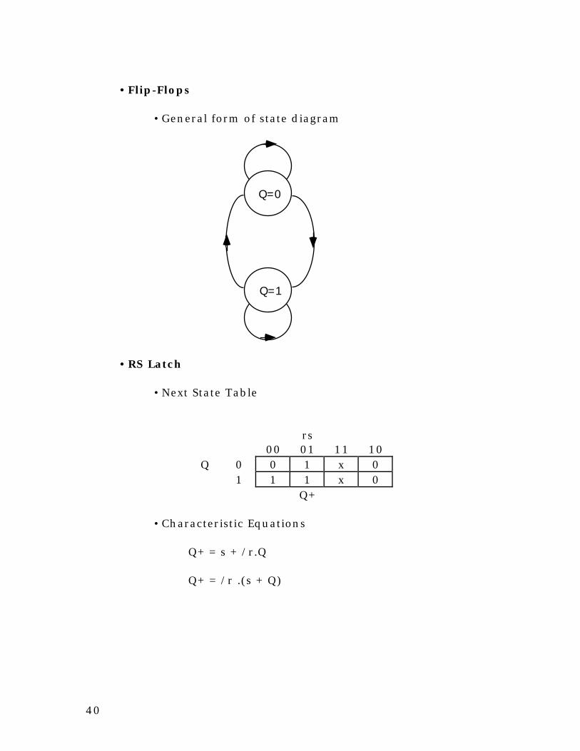
•Flip-Flops
•General form of state diagram
Q=1
Q=0
•RS Latch
•Next State Table
rs00 01 11 10
Q 0 0 1 x 01 1 1 x 0
Q+
•Characteristic Equations
Q+ = s + /r.Q
Q+ = /r .(s + Q)
41
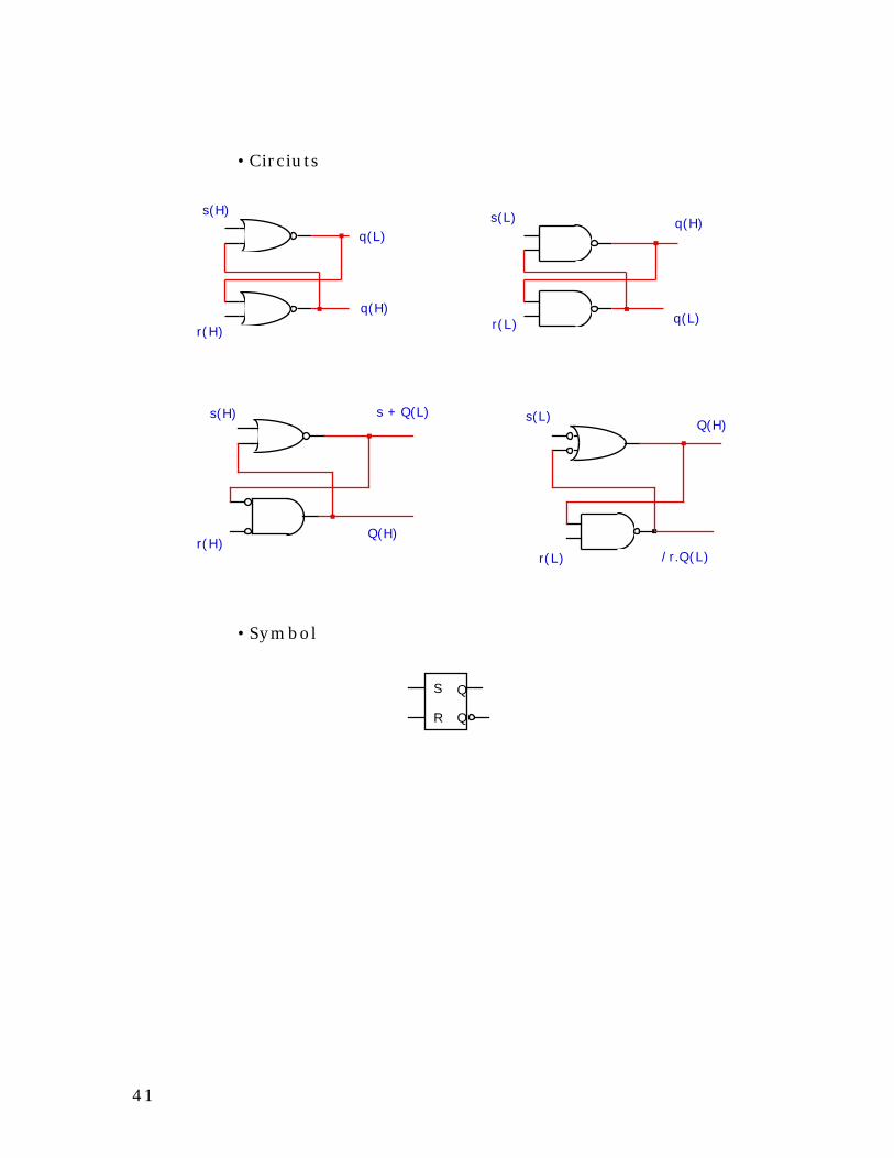
•Circiuts
s(H)
r(H)
s(L)
r(L)q(H)
q(L)q(H)
q(L)
s(L)
r(L)
Q(H)
/r.Q(L)
s(H)
Q(H)r(H)
s + Q(L)
•Symbol
Q
QR
S

42
•RS Latch with enable
Q
QR
S Q
QR
SC
S
R
C
•Circuit •Symbol
•Timing Diagram
C
transparent transparent
S
Q
Tsetup Thold
Tprop
Device is often called a level sensitive transparent latch

43
•D Latch
Q
QR
SC
D
C
Q
Q
D
C
•Circiut•Symbol
•JK Master/Slave Flip_Flop
•Next State K-map
JK00 01 11 10
Q 0 0 0 1 11 1 0 0 1
Q+
•Characteristic Equation
Q+ = J./Q + /K.Q
•Excitation K-map for RS implementation
JK00 01 11 10
Q 0 X0 X0 01 011 0X 10 10 0X
RS
•Excitation Equations
R = K.Q S = J./Q

44
Q
QR
SC
Q
QR
SC
C
Q
Q
JKJ
Q
/Q
K
C/C
•Circuit•Symbol
P
/P
•Comments
The left latch can set or reset while C = 1 andhence
the new state may not be determined by values of J,K at time of clock negative edge. This is the 1s or
0s catching problem.
Example of 1s catching: If Q = 0 and J = 1 momentarily while C = 1 and J,K = 0 on clock negative edge, the new Q will be 1 rather than 0.
Example of 0s catching: If Q = 1 and K = 1 momentarily while C = 1 and J,K = 0 on clock negative edge, the new Q will be 0 rather than 1.

45
•Edge triggered D flip-flops
•Characteristic equation
Q+ = D
•Symbols
D
C
Q
Q
D
C
Q
Q
+ edge triggered D flip-flop
-edge triggered D flip-flop

46
• Edge triggered JK flip-flop
•D flip flop excitation equation
D = J./Q + /K.Q
D
C
Q
Q
C
Q
Q
JK
J
/K
•Circuit
•Symbol

47
•Data Transfer
•Single phase clocking
•Typical Circuit
D
C
Q
Q
D
C
Q
Q
X
C
•Key Parameters
Tsetup, Thold, Tprop, Tskew, Tclock
•Timing Diagram
C @ left ff
C @ right ff
Tskew
Tsetup for right ff Thold for right ff
X Tprop
•So that right ff gets old value of left ff:Tprop for left ff > Tskew + Thold for right ff
•Tclock > Tprop for left ff + Tsetup for right ff

48
•Two-phase Clocking
•Used to tolerate more clock skew than single phase clocking. The cost is twice the number of
storage elements.
•Circuit
D
C
Q
Q
D
C
Q
Q
D
C
Q
Q
D
C
Q
Q
C1
C2
Stage2Stage1
•Input elements of each stage updated on + edge of C1.•Output elements of each stage updated on + edge of C2.
•May use + and - edges of a single clock if negative edge triggered flip-flops used for output stages.

49
•Finite State Machine Design
•Chapter 8 of text.
•Design Procedure
1. Understand problem-English descriptions-timing diagrams
2. Obtain abstract representation of the FSM-state diagrams-algorithmic state machine notation
3. Perform state minimization4. Perform state assignment5. Choose flip-flop types6. Implement

50
•Simple Design Example
•1. Design serial odd parity machine, ie, 1 output iff odd number of 1 bits have arrived.
•Timing diagram for a Moore Machine
clock
input
output

51
•2 State Diagram for Moore Machine
Odd [1]
Even [0]
reset
0
1
0
1
•3 to 6 Excitation Map for D flip-flop
Q0 1
Input 0 0 11 1 0
D
D = Q EOR Input
D
C
Q
QInput
Output

52
•Timing Diagram for a Meay Machine
clock
input
output
•State Diagram for a Mealy Machine
one
reset/0
two
0/0
1/1
0/1
1/0

53
•3 to 6Encode state one with Q = 0.Encode state two with Q = 1Choose + edge D flip-flop
•Excitation and Output Maps
Q0 1
Input 0 00 111 11 00
D/Output
D = Output = Q EOR Input
•Circuit
D
C
Q
QInput
Output

54
•Summary of Moore and Mealy Sequential Circuits
•For Moore: Outputs = Function(Present state).Therefore Outputs specified in state symbol of
state diagram. Output changes only after a logic delay following a state change.
•For Mealy:Outputs = Function(present state, Inputs).Therefore Outputs specified on arcs of state
diagram. Outputs may change whenever Inputs or Present state change. Because Outputs may change when Inputs change, the Outputs are not synchronous. May use an additional flip-flop to synchronize the outputs. This introduces a 1 cycle delay, however.
•Synchronized Mealy Circuit
PresentState
D
C
Q
QCInput
UnsynchronizedOutput
SynchronizedOutput
InputLogic
OutputLogic

55
•Numbers of States, Transitions and Outputs in FSMs
Let L = Number of flip-flopsM = Number of inputs linesN = Number of output lines
•Number of states
max number = 2L
min number = 1
•Number of transitions from a state
max number = 2M
min number = 1
•Number of transitions into a state
max number = 2M . 2L
min number = 0
•Number of ouput patterns
max number for Moore = min (2N, 2L)
max number for Mealy = min (2N, 2L+M)
min number = 1

56
•Algorithmic State Machine (ASM) Notation
•State diagram notation that explicitly specifies allbinary input and output patterns is limiting for large
circuits.
•ASM notation is an alternative more suited to large circuits.
•ASM notation uses a state block for each state as shownbelow
Fig 8.19
•Block may have 0 or more condition boxes and output boxes. Output boxes only used for Mealy machines. Outputs may be qualified as asserted H or L. Conditional outputs may be further qualified as being asserted immediately or upon next clock pulse.

57
•Example equivalent FSMs
figs 8.26 and 8.27

58
•Analysis of FSMs
•Given a circuit, derive an abstract representation such as a state diagram or ASM notation representation. Text describes Signal Trace Method and Next State/Output Function Analysis. The Signal Trace Method considers sample timing diagrams to derive state transition tables. The method is limited to small systems and is difficult to apply. We will ignore it.
•Next State/Output Function Analysis
•Example
Fig 8.33
•Observations
•State variables: A,B•Input: X•Output: Z•Circuit is unsynchronized Mealy

59
•Analysis
•Excitation Equations
D = (A + X)BJ = /A EOR XK = /X
•Output Equation
Z = /XB + XA
•Next State Equations
A+ = D = AB + BX
B+ = J/B + /KB for JK flip-flopA/BX + /A/B/X + BX
•Next state and Output Maps
Fig8.36
•ASM chart
Fig 8.37

60
•FSM Design Examples
•A Finite String Recognizer
A finite string recognizer has one input, X, and one output, Z. The output is asserted whenever the
input sequence ...010... has been observed providing the input sequence ...100... has not been observed.
•Understand problem
•Sample timing diagram assuming Mealy machine.
C
Z
X
•First try at state diagram
reset/0
0/0
1/0
0/1
1/0
0/0
0/0

61
•Final state diagram
S1
S2
S3
reset/0
0/0
1/0
0/1
1/0
0/0
0/0
0/01/1
0,1/0
1/0
1/0
S4
S5
S2
S3
S6

62
•Traffic Light Controller
•Farm road crosses a highway•signal, C, detects presence of a farm vehicle waiting to cross highway.•times between setting a timer with signal ST and the timer generating signals TS and TL are
used for the duration of yellow and the duration of green respectively.
•highway stays green unless farm vehicle detected.•highway green for a time never less than time determined by TL.
•Controller input signals
•reset•C cross highway•TS time short expired•TL time long expired
•Controller output signals•HG, HY, HR (green, yellow, red signals
for highway lights)•FG, FY, FR (green, yellow, red signals
for farm road)•ST set timer
•States
•S0 highway green, farmroad red•S1 highway yellow, farmroad red•S2 farmroad green, highway red•S3 farmroad yellow, highway red

63
•Typical timer signal timing
ST
TS
TL
clock

64
•ASM Chart
S0
S1
S2
S3
HG,FR
HY,FR
FG,HR
FY,HR
TL.C
ST
ST
ST
ST
TS
TL + /C
TS
1
0
1
1
1
0
0
0
reset

65
•State Diagram
reset
/TL + /C
/TS
/TL.C
/TS
TL.C/ST
TS/ST
TL + /C/ST
TS/ST
S0
S1
S2
S3

66
•Implementation
•A detailed implementation is described in Ch. 10.The following observations apply to
implementation:
*The inputs to the controller should be synchronized with the controller clock to
avoid metastability.
*A 74163 counter is the basis for a good timer.
*The excitation equations for the controller are functions of 5 variables. Deriving and
minimizing these is nontrivial.
•Digital Combination Lock
Design the controller for a 3-bit (mickey mouse) combinationlock as illustrated below.
Reset
eNter
Key-in
L0
L1
L2
Unlock
Error
Controller
The 3 bits provided to Unlock the lock are entered sequentially viathe Key-in input. A bit is entered by asserting eNter for 1 clockperiod once the selected value of Key-in has been established. TheKey-in sequence to unlock the lock is L0,L1,L2. If the correctsequence is entered Unlock is asserted. If the correct sequence is

67
not entered Error is asserted. The following state diagram can bederived.
start
idle0
idle1
idle2
idle4
idle5
idle3
[U] [E]
R
R + /N
/R.N.(K=L0) /R.N.(K/=L0)
/R
/N
/N
/R
/N
/N
RR
N.(K=L1)
N.(K/=L1)
N.(K=L2)
N.(K/=L2)
N
N
•Finite State Machine Optimization
We will study
•State Minimization-row-matching method-implication chart method
•State Assignment
•Flip-flop choice
•FSM partitioning

68
•State Minimization
In generating a state diagram for a FSM it is often the case thatmore states than are actually required are found. When this is thecase there are redundant equivalent states that can be eliminated togive a simpler yet equivalent FSM. The elimination of redundantequivalent states may result in the need for fewer state flip-flops ormay give rise to simpler excitation equations.
Two FSMs are equivalent if identical input sequences to the twomachines give identical output sequences.
Two states are equivalent if their next states and outputs areidentical. This definition is used to eliminate one of a pair ofequivalent states from a FSM.
•Row-matching Method
•repetitively compare all pairs of states using a next state table. Remove equivalent states as comparisons proceed.
•Example
present next state outputstate x=0 x=1 x=0 x=1S0 S1 S2 0 0S1 S3 S4 0 0S2 S5 S6 0 0S3 S7 S8 0 0S4 S9 S10 0 0S5 S11 S12 0 0S6 S13 S14 0 0S7 S0 S0 0 0S8 S0 S0 0 0S9 S0 S0 0 0S10 S0 S0 1 0S11 S0 S0 0 0S12 S0 S0 1 0S13 S0 S0 0 0S14 S0 S0 0 0

69
States S7, S8, S9, S11, S13, S14 are equivalent to say Sa.States S10 and S12 are equivalent to say state Sb.We therefore generate the following intermediate table.
present next state outputstate x=0 x=1 x=0 x=1S0 S1 S2 0 0S1 S3 S4 0 0S2 S5 S6 0 0S3 Sa Sa 0 0S4 Sa Sb 0 0S5 Sa Sb 0 0S6 Sa Sa 0 0Sa S0 S0 0 0Sb S0 S0 1 0
States S3 and S6 are equivalent to say Sc.States S4 and S5 are equivalent to say Sd.We therefore generate the following table.
present next state outputstate x=0 x=1 x=0 x=1S0 S1 S2 0 0S1 Sc Sd 0 0S2 Sd Sc 0 0Sc Sa Sa 0 0Sd Sa Sb 0 0Sa S0 S0 0 0Sb S0 S0 1 0
No further reduction can occur. Therefore this is the reduced state table.
When self loops are present, this method does not always give the most reduced FSM.

70
•Implication Chart Method
This method always gives the most reduced FSM but it is a little more complex than the row-matching method.
This method uses a matrix chart that show which states need to be equivalent for the states corresponding to the cells of the chart to be equivalent.
•Example
Next state tablepresent next state outputstate x=0 x=1 x=0 x=1S0 S1 S2 0 0S1 S3 S4 0 0S2 S5 S6 0 0S3 S0 S0 0 0S4 S0 S0 1 0S5 S0 S0 0 0S6 S0 S0 1 0
Initial Implication ChartS1 S1-S3
S2-S4S2 S1-S5
S2-S6S3-S5S4-S6
S3 S0-S1S0-S2
S0-S1S0-S4
S0-S5S0-S6
S4 X X X XS5 S0-S1
S0-S2S0-S3S0-S4
S0-S5S0-S6
S0-S0S0-S0
X
S6 X X X X S0-S0S0-S0
X
S0 S1 S2 S3 S4 S5

71
The cell corresponding to S3,S1, for example ,shows that S0 must be equivalent to S1 (indicated by S0-S1)and S0 must be equivalent to S4 (indicated by S0-S4) for S3 to be equivalent to S1. An X indicates the states corresponding to the cell
cannot be equivalent.
Systematically use the Xs in the implications chart to place place additional Xs in the chart. For example, since there is anX in the S2,S4 cell, we place an X in the S1, S0 cell because S1,S0 cannot be equivalent unless S2 and S4 are equivalent.
Final Implication Chart S1 XS2 X S3-S5
S4-S6S3 X X XS4 X X X XS5 X X X S0-S0
S0-S0X
S6 X X X X S0-S0S0-S0
X
S0 S1 S2 S3 S4 S5
Therefore S4 and S6 are equivalent to say Sa, S3 and S5 are equivalent to say Sb, and S1 and S2 are equivalent to say Sc. The next state table therefore becomes
Reduced next state tablepresent next state outputstate x=0 x=1 x=0 x=1S0 Sc Sc 0 0Sc Sb Sa 0 0Sb S0 S0 0 0Sa S0 S0 1 0
72
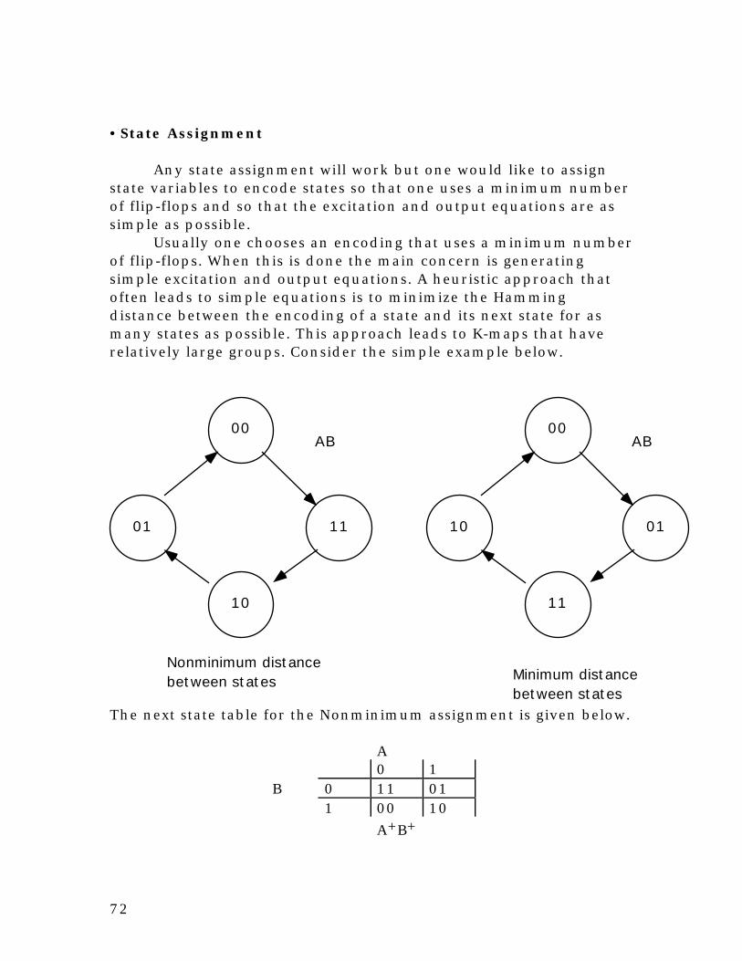
•State Assignment
Any state assignment will work but one would like to assignstate variables to encode states so that one uses a minimum numberof flip-flops and so that the excitation and output equations are assimple as possible.
Usually one chooses an encoding that uses a minimum numberof flip-flops. When this is done the main concern is generatingsimple excitation and output equations. A heuristic approach thatoften leads to simple equations is to minimize the Hammingdistance between the encoding of a state and its next state for asmany states as possible. This approach leads to K-maps that haverelatively large groups. Consider the simple example below.
AB AB00
0110
11
00
10
01 11
Nonminimum distancebetween states Minimum distance
between statesThe next state table for the Nonminimum assignment is given below.
A0 1
B 0 11 011 00 10
A+B+

73
The next state equation for A+ does not simplify.
The next state table for the minimum assignment is given below.
A0 1
B 0 01 001 11 10
A+B+
The next state equations for both A+ and B+ do simplify.
When assigning states to a state diagram the following prioritiesshould be given to minimizing the Hamming distance between thestates under consideration.
Highest Priority
A B
i/j i/k
When 2 or more state have the same next state for the sameinputs, the highest priority should be given to minimizing thedistance between the present states.

74
Medium Priority
A B
When 2 or more states are the next states of a common state,medium priority should be given to minimizing the distance betweenthe next states.
Lowest Priority
A B
i/j i/j
When 2 or more states have the same outputs for the sameinputs, the distance between the states should be minimized.

75
Example of using the prioritiesConsider assigning states to the following state diagram.
0/0 1/0
0,1/0
0,1/0
1/0 1/0
1/0
1/0
0/0 0/0
0/0
0/1
S0
S1 S2
S3 S4
S5 S6
Highest priority for minimum distance.
S3,S4S5,S6
Medium priority for minimum distance.
S1,S2S3,S4S3,S4S5,S6
Lowest priority for minimum distance.
for 0/0 S0,S1,S2,S3,S4,S5for 1/0 S0,S1,S2,S3,S4,S5,S6
With the following assignment, all the high and medium prioritiiesand most of the lowest priorities are distance 1.
Q1Q2
00 01 11 10Q3 0 S0 S1 S3

76
1 S5 S2 S4 S6
One-Hot Encodings
With one-hot encoding, only one state flip-flop is set for eachstate. The Hamming distance between any two states is thus 2. Thisis not a dense encoding since more flip-flops are used than requiredbut assignment and output equation generation is easy.
•Flip-Flop Choice
D flip-flop FSMs are easiest to design but JKs may lead tosimpler circuits. It is not common to use a mix of flip-flop types.There are no guidelines for choosing flip-flop types. The type isoften determined by the type of flip-flop available with thetechnology to be used for implementation. For example, most PALand the Xilinx LCAs have D flip-flops but not JK flip-flops.
•Finite State Machine Partitioning
For various reasons it may be necessary to partition a FSM into2 or more FSMs. Consider partitioning the following FSM into a leftFSM and and a right FSM along the dashed line.
S1
S2
S3 S4
S5
S6
C1
C2
C3
C4C5

77
When the machine is in the states of the left machine the rightmachine is idle and visa versa. When a transisition occurs from theleft machine being active to the right machine being active the leftmachine enters an introduced idle state Sa and the right machineleaves its introduced idle state Sb. The reverse happens when atransition occurs from the right machine to the left machine. Theintroduced states Sa and Sb together with the conditions for makingthe transitions are shown below.
S1
S2
S3
C2.S6
C3 + C5
C4
Sa
C1
C2.S6
S4
S5
S6C1.S1
C5.S2
C2
SbC3.S2+C4.S3
C1.S1+C3.S2+C4.S3+C5.S2Note carefully how the conditions are specified to enter and leavethe idle states. Note also that some of the transition conditions andstate variables must be available in both the left and the right FSMs.

78
Example
Consider partitioning the up/down counter shown below in itsoriginal form and its partitioned form. Self loops are not shown butevery state has a self loop that is taken when the explicit transitionsare not taken.
S1
S3
S5S0
S2
S4
UU
U
U U
U
D
D
D
D
D
D
S0
S2
S4S1
S3
S5
Sa Sb
D
U
U.S2UU
U
DD
D
D
U
D
D.S0
U.S5
D.S3

79
•FSM Implementation
This portion of the course deals with generating circuits fromabstract FSM representations such as state diagrams and ASMnotation. In theory a CAD package should be able to provide themapping from a state diagram, for example, to a circuit. This is notyet widely available, however, and it is usually necessary to generatelogic equations from the state diagram that are suitable for theavailable hardware or CAD sytem that is to be used.
When using discrete logic such as TTL the circuit components mustbe selected before the appropriate equations can be generated. Thisrequires an understanding of the components available in the TTLfamily.
When using custom VLSI or PLDs some knowledge of the targethardware is usually required and a good knowledge of the CADsystem is required. If the CAD system is low level like Xilinx Xact, forexample, considerable knowledge of the hardware is required togenerate the necessary design equations. If the CAD system is highlevel like VHDL, for example, little detailed knowledge of the targethardware is often required.
Chapter 10 of the text gives several examples of how the logicequations for some sample FSMs are written in the ABEL CADlanguage for the implementation of PAL circuits. Some knowledge ofthe target PAL is desireable in order to program equations that mapefficiently to the available PAL hardware.
A sample VHDL program is given below. The program gives a precisedescription of some hardware. The program can be compiled togenerate data for prescribed hardware, the program can be checkedfor syntax errors and the program can be used as a source of datafor circuit simulation.

80
•VHDL
entity and2 isport (a,b : in bit; y : out bit);
end and2;
architecture basic of and2 isbegin
and2_behavior : process isbegin
y<= a and b after 2 ns;wait on a,b;
end process and2_behavior;end architecture basic;
entity or2 isport (a,b : in bit; y : out bit);
end or2;
architecture basic of or2 isbegin
or2_behavior : process isbegin
y<= a or b after 2 ns;wait on a,b;
end process or2_behavior;end architecture basic;
entity inv1 isport (a : in bit; y : out bit);
end inv1;
architecture basic of inv1 isbegin
inv1_behavior : process isbegin
y<= not a after 2 ns;wait on a;
end process inv1_behavior;end architecture basic;
81
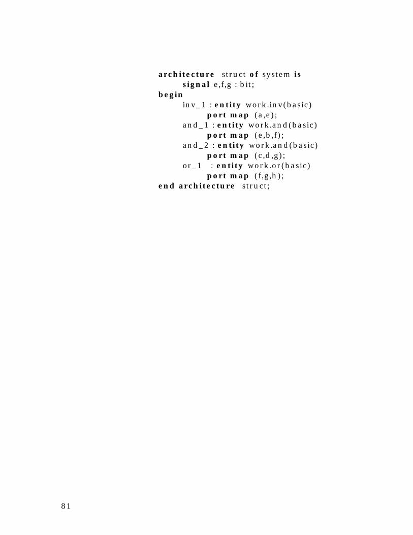
architecture struct of system issignal e,f,g : bit;
begininv_1 : entity work.inv(basic)
port map (a,e);and_1 : entity work.and(basic)
port map (e,b,f);and_2 : entity work.and(basic)
port map (c,d,g);or_1 : entity work.or(basic)
port map (f,g,h);end architecture struct;

82
•Traffic Light Controller Implementation
Consider the traffic light controller state diagram given below. Thisstate diagram is the same as that developed earlier except theconditions for self looping have been deleted since they can beimplied from the conditions for not self looping.
reset
TL.C/ST
TS/ST
TL + /C/ST
TS/ST
S0
S1
S2
S3
Let the 4 states be encoded by state variables Q1 and Q0. Thecontroller has three inputs TL, TS, and C, It has one conditionaloutput ST and 6 unconditional outputs, HG,HR,HY,FG,FR,FY to drivethe lights that are a function only of the state.

83
Following the state assignment priorities suggests that S1 and S3should be unit distance. We will use the assignmentS0--Q1Q0 = 00, S1--Q1Q0 = 01, S2--Q1Q0 = 10, S3--Q1Q0 = 11.
Assume that all inputs are synchronous and that everything in thesystem is + edge triggered.
A suitable car detector circuit to generate the input, C , is givenbelow.
car
clock
debouncer synchronizer
/reset
D
C
S
R
Q
Q+5V
+5V
C
The timer circuit to generate TS and TL is best built with one ormore counters to provide the time resolution required. Let usassume that the 4 bit 74163 synchronous counter is adequate. Thesample timing diagram given previously is repeated below.
ST
TS
TL
clock
A simple circuit that generates TS and TL in response to ST is givenbelow.

84
cl ock
/ST
QAQBQCQD
163RCO
PT
ABCD
LOAD
CLR
CLK
107
1
9
2
3456
14131211
15
+5V
TS
TL
ST
Outputlogic
For TS to go low for 7 clock cycles, for example, the output logic is
/TS = ST + zero + one + two + three + four + five
= ST + /QD./QC + /QD./QB
The output logic for TL is similar.
Note that this timer always counts. This is okay in this applicationsince the controller always clears the counter with a ST pulse beforewaiting for TS and TL to go high.
The controller equations are determined from the state diagram.One way to do this is to construct next state tables or next state K-maps. These are functions of 5 variables and are rather inconvenientto construct and use. For systems with even more state variables andinputs this approach is impractical. An alternate, and often betterapproach, is to write the next state equations directly from the statediagram by considering all the transition to true values of the statevariables. Our state diagram labeled as conveniently as possible isgiven below.

85
reset
TL.C/ST
TS/ST
TL + /C/ST
TS/ST
Q1Q0
Q1Q0
Q1Q0
Q1Q0
From the table we write
Q0+ = /Q1./Q0.TL.C + /Q1.Q0./TS +Q1./Q0.(TL + /C) + Q1.Q0./TS
Q1+ = /Q1.Q0.TS + Q1./Q0./Tl.C +Q1./Q0.(TL + /C) + Q1.Q0./TS
ST = /Q1./Q0.TL.C + /Q1.Q0.TS + Q1./Q0.(TL + /C) + Q1.Q0.TS

86
The excitation equations are obtained from the next state equationsby using the characteristic equations of the chosen flip-flops. Theexcitation equations may then be simplified by the usual means(algebra, Kmaps, CAD). For example, if a JK flip-flop is used for Q0then
Q0+ = J0./Q0 + /K0.Q0
Therefore
J0 = /Q1.TL.C + Q1.(TL + /C) = Q1./C + TL.C
/K0 = /Q1./TS + Q1./TS = /TS
K0 = TS
•Controller Implementation using a 74163 Counter
With the state assignment that has been made it is evident that a 2bit binary up counter that idles, under specified conditions, in itscurrent state could be used for the controller. That is
enable_count = /Q1./Q0.TL.C + /Q1.Q0.TS + Q1./Q0.(TL + /C) + Q1.Q0.TS
This equation can be implemented neatly with a multiplexor asshown below.

87
/reset
TL
C
TL
/C
TS
Q0
Q1
enable_count
B1B2B3
B0
A3A2A1A0
153GA
GB
YA
YB
S1 SO
6543
1
10111213
15
7
9
QAQBQCQD
163RCO
PT
ABCD
LOAD
CLR
CLK
107
1
9
2
3456
14131211
15+5V

88
•Computer Organization
The next portion of the course is concerned with the organization ofsimple computers. We will consider
register transfer notationdatapath organizationsmemory interfacingsimple controller design
•Register Transfer Notation
It is common to use a register transfer notation to specify,rather abstractly, register transfers and other operations that mustoccur within a computer. Each register transfer or operation that isspecified usually gives rise to the generation of one or more controlsignals to actually cause the transfer or operation to take place.Usually hardware is provided to carry out the transfers andoperations that are specified.
The following are examples of register transfer notation.
Notation Meaning
A -> B transfer the contents of the A register to the B
register. A retains its value
A + B -> A transfer A plus B to A
IF A<15:14> = 10 If A bits 15,14 = 10 thenTHEN A<13:0> -> B transfer bits 13 to 0 to the
B
1-> Reset Set Reset to 1
The use of this notation will become clear with examples thatfollow.

89
•Datapath Organizations
The datapath portion of a digital system (computer) containsthe registers, processing elements and interconnections that arerequired to carry out the operations the machine is intended toperform. For a fast computer capable of many operations thedatapath is extensive and may contain thousands of registers,interconnections and processing elements. We will illustrate many ofthe relevant principles by considering in detail a simple fourinstruction computer. Little effort will be devoted to reducing theclock cycles per instruction to make the computer fast. In modernreal computers a great deal of effort is devoted to pipelining andparallelism to make the machine fast.
Our illustrative computer, call it Illc, has a 16 bit word, asingle accumulator and four machine instructions LD, ST, ADD andBRN with an instruction format as shown below.
15 14 0
addressopcode
ILLC INSTRUCTION FORMAT
The instructions are defined as follows:
op-code mnemonic operation
00 LD XXX Memory[XXX] -> AC
01 ST XXX AC -> Memory[XXX]
10 ADD XXX AC + Memory[XXX] -> AC
11 BRN XXX IF AC<15>=1 THEN XXX -> PC
Although it would be painful, any algorithm can be coded with theseinstructions!

90
Illc, like any computer, is comprised of atleast a cpu and memory.The cpu gets instructions and data from memory and stores data inmemory. Hence a memory interface and protocol for transfersbetween the cpu and memory must be defined. The cpu requires aset of registers to execute the machine instructions and anarithmetic and logic unit (alu) consisting of atleast an adder to carryout the ADD instruction. The following steps to execute aninstruction seem evident.
1. fetch the next instruction from memory
2. decode the instruction
3. execute the instruction
From these steps, one can envision the need for a register to keeptrack of the next instruction to be executed( the program counterPC),a register to hold a memory address( the memory address registerMAR), a register to buffer instructions and data moving between thecpu and memory (the memory buffer register MBR) and a register tohold an instruction while it is being decoded by the cpu (theinstruction register IR). One way to organize these registers isshown below.
91
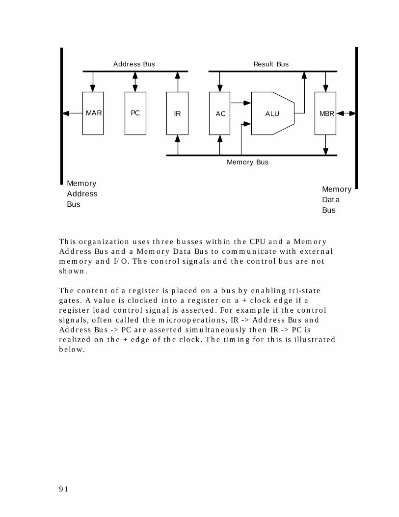
MAR PC IR AC ALU MBR
Address Bus Result Bus
Memory Bus
MemoryAddressBus
MemoryDataBus
This organization uses three busses within the CPU and a MemoryAddress Bus and a Memory Data Bus to communicate with externalmemory and I/O. The control signals and the control bus are notshown.
The content of a register is placed on a bus by enabling tri-stategates. A value is clocked into a register on a + clock edge if aregister load control signal is asserted. For example if the controlsignals, often called the microoperations, IR -> Address Bus andAddress Bus -> PC are asserted simultaneously then IR -> PC isrealized on the + edge of the clock. The timing for this is illustratedbelow.

92
Clock
IR -> Address Bus
Address Bus -> PC

93
The memory interface for Illc is illustrated below.
Memory
read
request
wait
Memory Data Bus
Memory Address Bus
The signal name read is used rather than the morecommon name read/write .

94
ReadCycle
wait
wait/MAR->Memory Address Bus,read,request
wait
wait
wait
wait/MAR->Memory Address Bus,read,request
/Memory Data Bus->MBR
Comment The memory normally asserts wait. Wait is unasserted following a request when memory completes the request.

95
WriteCycle
wait
wait/MAR->Memory Address Bus,MBR->Memory Data Bus,request
wait
wait
wait
wait/MAR->Memory Address Bus,MBR->Memory Data Bus,request
Comment The memory normally asserts wait. Wait is unasserted following a request when memory completes the request.

96
rese
t/0
->PC
rese
t/
rese
t/PC
->M
AR,
PC+
1->
PC
mem
ory
read
cyc
le wai
t/M
BR-
>IR
IR<
15
:14
>=
00
/IR
<1
3:0
>->
MA
R
mem
ory
read
cyc
le
wai
t/M
BR-
>A
C
mem
ory
writ
e cy
cle
wai
t/
IR<
15
:14
>=
01
/IR
<1
3:0
>->
MA
R,A
C->
MBR
IR<
15
:14
>=
10
/IR
<1
3:0
>->
MA
R
mem
ory
read
cyc
le
wai
t/M
BR+
AC->
AC
IR<
15
:14
>=
11
.A
C<
15
>=
1/
IR<
13
:0>
->PC
Inst
ruct
ion
Fetc
h
Inst
ruct
ion
Dec
ode
Inst
ruct
ion
Exec
utio
n
LDST
AD
DBRN

97
•Mealy and Moore Implementations of Controller
A state diagram for a Mealy FSM controller was given in thelast section. The controller can be implemented directly by thetechniques we have studied. To do this we must be sure the datapathand memory are synchronized with the controller. We should alsonote that because the fetch memory read cycle does not proceeduntil Wait is asserted and does not conclude until Wait is asserted, itis not necessary to wait for Wait to be asserted at the beginning andend of the execution memory cycles.
The Mealy state diagram can be converted to a Moore statediagram as given in the text. Another possibility is to implement theMealy state diagram as a synchronous Mealy machine. This may benecessary if the datapath or memory are not synchronized with thecontroller.
•Counter Implementation of Controller
Another possibility for implementing the controller is to use asynchronous counter with a hold, clear and load capability such asthe 74163. The text calls this a hybrid junp counter controller. Forthis approach, it is desireable to assign states so that most nextstates are reached by simply incrementing the counter. A suitablestate assignment is given in the following abbreviated state diagramof the Mealy controller with simplified execution memory cycles. Aschematic of the main part of the controller is given in thesubsequent figure. The equations for HOLD, CLR and LOAD can beeasily obtained from the state diagram. The jump states, 5, 8, 10, 13that must be loaded into the counter are generated as a function ofthe op-code as contained in IR15 and IR14. The 74154 encoderencodes the controller states as S0, S1,........S13. Each control signalthat is required is generated as a function of a controller inputs andthe state signals Si. For example
Memory Data Bus-->MBR = /Wait.(S2 + S6 + S11)

98
Fig 12.16
Simplified Mealy Controller with state assignmentsuitable for counter implementation

99
Fig 12.17
Counter based Controller

100
•ROM Based Controllers
Rather than use counters and combinational logic todetermine the next state variables and output variables (controlsignals), it is common to use a ROM and simply look up the valuesof the next state and output variables. When this is done thecorrespondence between a classical FSM and a ROM based FSM isgiven below.
S+
S
I
Z
Nextstatelogic
Outputlogic
D ffstatememory
Classical FSM
I
S+S
ROM
Z
D ffstatememory
ROM based FSM

101
With a ROM based FSM controller, the Mealy state diagramgiven above requires 28 = 256 words of ROM since there a 4 statevariables and 4 input variables, wait, IR15, IR14, and AC15 thatdetermine the branching. Each word of ROM is 26 bits to store the 4next state variables and the 22 possible output control signals.These figures assume reset is done separately.
The portion of the words of ROM that contains the controlsignals for the data path, when talking about computers, is called amicroinstruction and all the microinstructions form amicroprogram. Such a computer is referred to as a microprogramcontrolled computer. Such a controller implementation is veryflexible because it is possible to alter the control signals by simplychanging the ROM. No circuit changes are required.
For fast computers a fast ROM is required. To minimize thecost of the ROM there is usually incentive to minimize its size.Through the use of multiplexors, decoders and external logic it isusually possible to reduce both the number of words of ROM andthe word length.
•Reduction of number of ROM words
With the ROM based controller described above, there can be16 different next states for each current state. However, the statediagram shows a most 4 different next states for a current state.Hence 2 multiplexors and possibly some combinational logic, asshown below, could be used to generate 2 address bits as a functionof the inputs for each current state. This gives rise to the need for a64 X 26 ROM

102
I
S+S
ROM
Z
D ffstatememory
ROM based FSM with Mux Input
logicI
mux
mux
For example, when the current state is 4 corresponding to theinstruction decode state, OD, the mux outputs would be driven fromIR15 and IR14 so that the correct next state can be read from theROM.
Another possibility for reducing ROM size is to store severalnext states in a ROM word and use a combination of bits in a ROMword and multiplexors to select the required next state. Consider,for example, the following ROM word and hardware configuration.

103
a b A0 A1 A2 A3 Control bits
mux control bits
4 possible next states
S+S
ROM
Z
D ffstatememory
ROM based FSM with Mux Selection of Next State
A0,A1,A2,A3mux
a,b
mux
mux
Inputs
This configuration requires only 16 words of ROM but each word is2 + 16 + 22 = 40 bits long.
The above techniques are used to reduce the number ofrequired ROM words. The number of control bits can be reduced byencoding groups of control bits that are never assertedsimultaneously and then using an external decoder to generate therequired control signals. Extra words of ROM may be used so thatmore encoding can be achieved. This can give rise to many shortwords of ROM and is called vertical microcoding. If little use of

104
encoding of the control signals is used, the number of wordsrequired is small but the word length is long. This is calledhorizontal microcoding.
Related Documents