Clemson University TigerPrints All eses eses 5-2015 Computational Modeling of Alternating Current Potential Drop Measurement for Crack Detection of Multi-Functional Ceramic Coated Structures Simha Sandeep Rao Clemson University Follow this and additional works at: hps://tigerprints.clemson.edu/all_theses Part of the Mechanical Engineering Commons is esis is brought to you for free and open access by the eses at TigerPrints. It has been accepted for inclusion in All eses by an authorized administrator of TigerPrints. For more information, please contact [email protected]. Recommended Citation Rao, Simha Sandeep, "Computational Modeling of Alternating Current Potential Drop Measurement for Crack Detection of Multi- Functional Ceramic Coated Structures" (2015). All eses. 2158. hps://tigerprints.clemson.edu/all_theses/2158

Welcome message from author
This document is posted to help you gain knowledge. Please leave a comment to let me know what you think about it! Share it to your friends and learn new things together.
Transcript
Clemson UniversityTigerPrints
All Theses Theses
5-2015
Computational Modeling of Alternating CurrentPotential Drop Measurement for Crack Detectionof Multi-Functional Ceramic Coated StructuresSimha Sandeep RaoClemson University
Follow this and additional works at: https://tigerprints.clemson.edu/all_theses
Part of the Mechanical Engineering Commons
This Thesis is brought to you for free and open access by the Theses at TigerPrints. It has been accepted for inclusion in All Theses by an authorizedadministrator of TigerPrints. For more information, please contact [email protected].
Recommended CitationRao, Simha Sandeep, "Computational Modeling of Alternating Current Potential Drop Measurement for Crack Detection of Multi-Functional Ceramic Coated Structures" (2015). All Theses. 2158.https://tigerprints.clemson.edu/all_theses/2158
COMPUTATIONAL MODELING OF ALTERNATING
CURRENT POTENTIAL DROP MEASUREMENT FOR
CRACK DETECTION OF MULTI-FUNCTIONAL CERAMIC
COATED STRUCTURES
A Thesis
Presented to
The Graduate School of
Clemson University
In Partial Fulfillment
of the Requirements for the Degree
Master of Science
Mechanical Engineering
by
Simha Sandeep Rao
May 2015
Accepted by: Dr. Huijuan Zhao, Committee Chair
Dr. Fei Peng
Dr. Gang Li
ii
ABSTRACT
Non-destructive testing and evaluation (NDT&E) is a set of techniques commonly
used to evaluate a material for the presence of any flaws without actually degrading the
material itself. The Alternating Current Potential Drop (ACPD) test method is one of the
NDT surface methods used to determine the electrically insulating defects beneath the
surface by injection of currents in the structure and measurement of the resulting voltage
difference between two or more points on the surface. The presence of defects generally
increases the resistance of the structure and hence causes the drop of measured voltage.
The inversion of this data can give information about the size and shape of the defects.
In the petrochemical and power generation industries, ceramic coatings have been
used to be applied to pipe lines in order to increase the strength and high temperature
resistance, as well as prevent the pipe lines from corrosion and oxidation. However,
traditional ceramic coating materials are electrically insulating. The ACPD testing method
cannot be adopted for the NDT purpose. In order to overcome this disadvantage, we
proposed a concept of a multi-functional ceramic coating material, in which the metal
nanoparticles (such as Nickel) can be uniformly embedded into the ceramic matrix
(mullite). This multi-functional ceramic matrix nanocomposite can conduct current via
tunneling when the percolation threshold of the filler phase is reached. Therefore, the
ACPD test method can still be adopted to predict the defect and crack beneath the surface.
iii
In this research, we adopt the commercial finite element package, COMSOL
Multiphysics, to first understand the mechanism of the ACPD method (electromagnetic
coupling, skin effect and proximity effect) by the two parallel conductor’s model; then
investigate the ACPD co-planar conductor model and understand the effect of the ceramic
coating material on the sensing signal with various coating conductivities, permeability’s
and frequencies. Finally, we draw conclusions and make proposals for future research.
iv
ACKNOWLEDGEMENTS
Firstly I would like to thank Dr. Huijuan Zhao for her inputs and support throughout
these two years as my graduate advisor. Her inputs have been invaluable to my research,
and a source of inspiration to me. I would also like to thank my committee members, Dr.
Fei Peng and Dr. Gang Li for their support and inputs to my research.
I would like to thank the COMSOL support team who has provided me with
detailed information about the software and greatly assisted me in my research.
I would also like to thank Clemson University for providing me with all the
resources and a conductive atmosphere to carry out my research in an organized fashion.
Additionally, I would like to take this opportunity to thank all my other professors who
have been of great support to me during my coursework.
v
TABLE OF CONTENTS
Page
TITLE PAGE ................................................................................................ i
ABSTRACT ................................................................................................. ii
ACKNOWLEDGEMENTS ........................................................................ iv
TABLE OF CONTENTS ............................................................................. v
LIST OF TABLES ..................................................................................... vii
LIST OF FIGURES .................................................................................. viii
CHAPTER
1. BACKGROUND AND MOTIVATION .......................................... 1
1.1 Non-Destructive Testing and Evaluation ............................... 1
1.2 Quantum Tunneling and Percolation Threshold ..................... 9
1.3 Motivation and Research Objectives .................................... 10
2. RESEARCH METHOD .................................................................. 12
2.1 Introduction to Electromagnetics .......................................... 12
2.1.1 Skin Effect ...................................................................... 14
2.1.2 Proximity Effect .............................................................. 20
2.2 Numerical Simulation Method ............................................. 22
3. PARALLEL CONDUCTOR MODEL ........................................... 24
3.1 Mesh Convergence Analysis ................................................ 24
3.2 Skin Effect ............................................................................ 26
3.3 Proximity Effect .................................................................... 28
vi
Table of Contents (continued)
Page
3.4 Proximity Effect between Two Different Conductors............ 30
3.5 Conclusions ............................................................................. 36
4. CO-PLANAR ELECTRODE MODEL ................................................ 37
4.1 Model Setup and Meshing Analysis ....................................... 37
4.2 Effect of the Coating ............................................................... 40
4.3 Investigation on Coating Material Selection .......................... 43
4.4 Simulation Limitation: Boundary Coupling Effect ................ 46
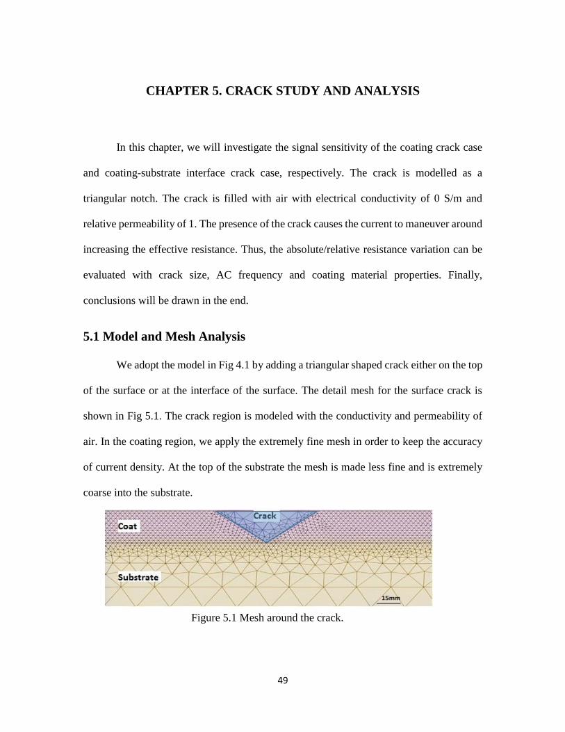
5. CRACK STUDY AND ANALYSIS ..................................................... 49
5.1 Meshing Analysis ................................................................... 49
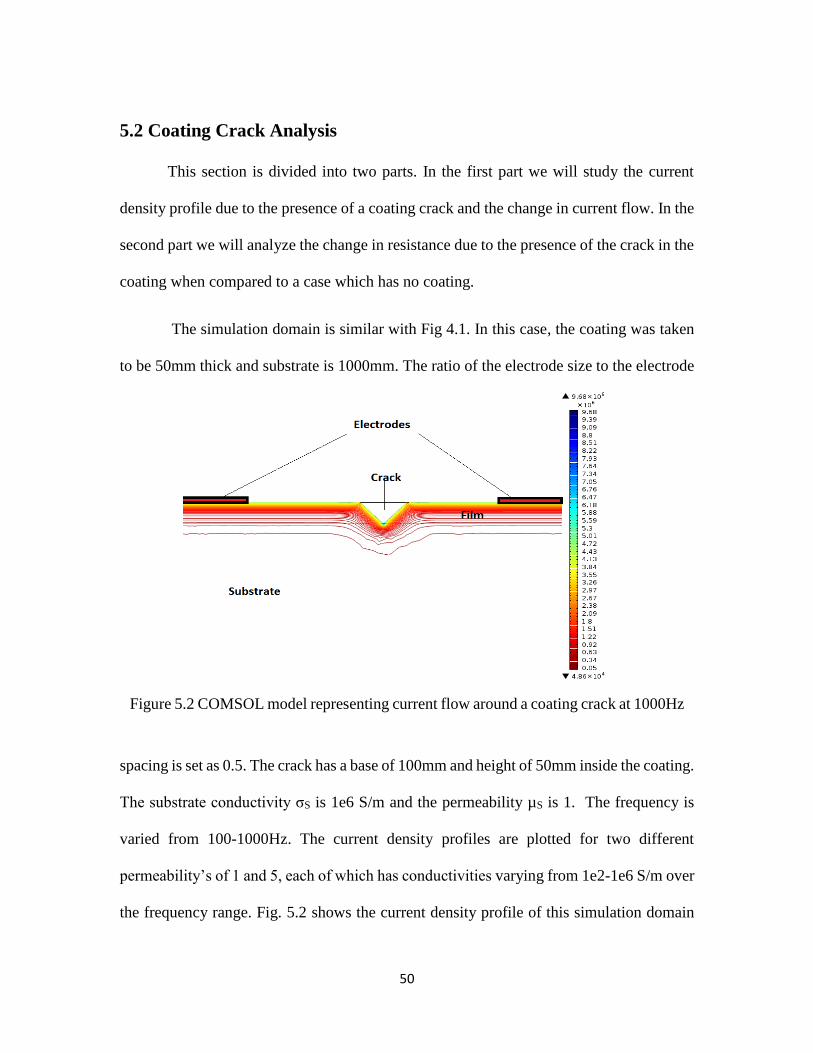
5.2 Coating Crack Analysis .......................................................... 50
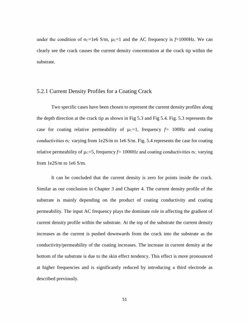
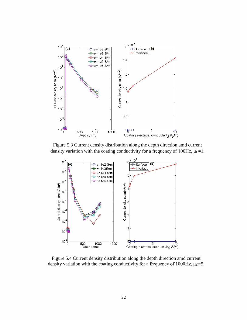
5.2.1 Current Density Profiles for a Coating Crack .................. 51
5.2.2 Resistance Calculation for a Coating Crack ..................... 53
5.3 Interface Crack Analysis ......................................................... 54
5.3.1 Current Density Profiles for an Interface Crack ............... 55
5.3.2 Impedance Calculation for an Interface Crack ................. 56
6. CONCLUSION AND FUTURE WORK .............................................. 58
6.1 Accomplishments.................................................................... 58
6.2 Conclusions ............................................................................. 59
6.3 Scope for future work ............................................................. 60
REFERENCES .......................................................................................... 61
vii
LIST OF TABLES
Table Page
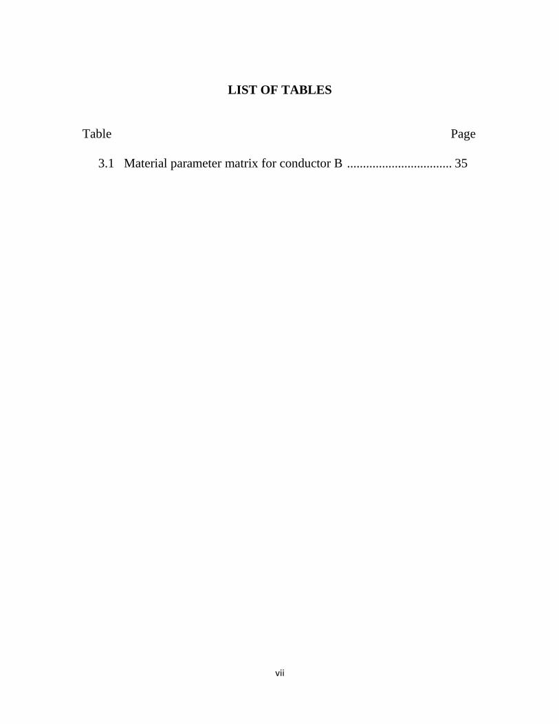
3.1 Material parameter matrix for conductor B ................................. 35
viii
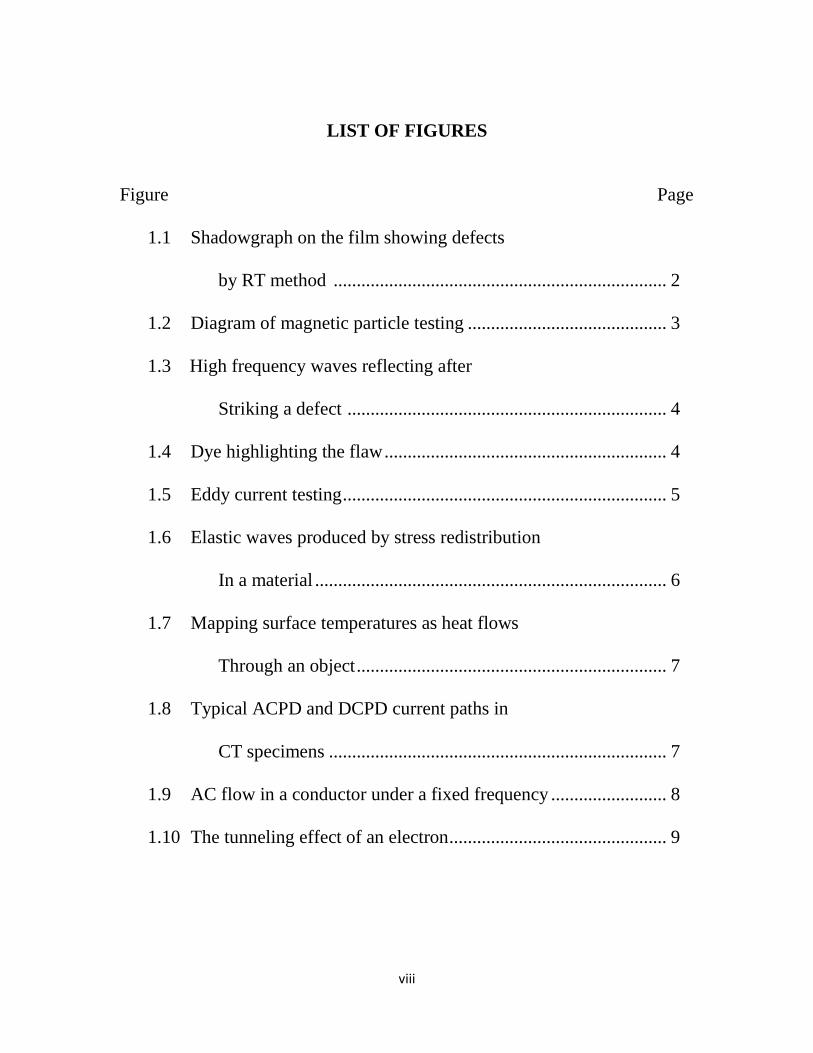
LIST OF FIGURES
Figure Page
1.1 Shadowgraph on the film showing defects
by RT method ........................................................................ 2
1.2 Diagram of magnetic particle testing ........................................... 3
1.3 High frequency waves reflecting after
Striking a defect ..................................................................... 4
1.4 Dye highlighting the flaw ............................................................. 4
1.5 Eddy current testing ...................................................................... 5
1.6 Elastic waves produced by stress redistribution
In a material ............................................................................ 6
1.7 Mapping surface temperatures as heat flows
Through an object ................................................................... 7
1.8 Typical ACPD and DCPD current paths in
CT specimens ......................................................................... 7
1.9 AC flow in a conductor under a fixed frequency ......................... 8
1.10 The tunneling effect of an electron ............................................... 9
ix
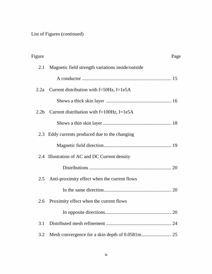
List of Figures (continued)
Figure Page
2.1 Magnetic field strength variations inside/outside
A conductor .......................................................................... 15
2.2a Current distribution with f=50Hz, I=1e5A
Shows a thick skin layer ...................................................... 16
2.2b Current distribution with f=100Hz, I=1e5A
Shows a thin skin layer ......................................................... 18
2.3 Eddy currents produced due to the changing
Magnetic field direction ........................................................ 19
2.4 Illustration of AC and DC Current density
Distributions .................................................................... 20
2.5 Anti-proximity effect when the current flows
In the same direction ........................................................ 20
2.6 Proximity effect when the current flows
In opposite directions ....................................................... 20
3.1 Distributed mesh refinement ...................................................... 24
3.2 Mesh convergence for a skin depth of 0.0581m ......................... 25
x
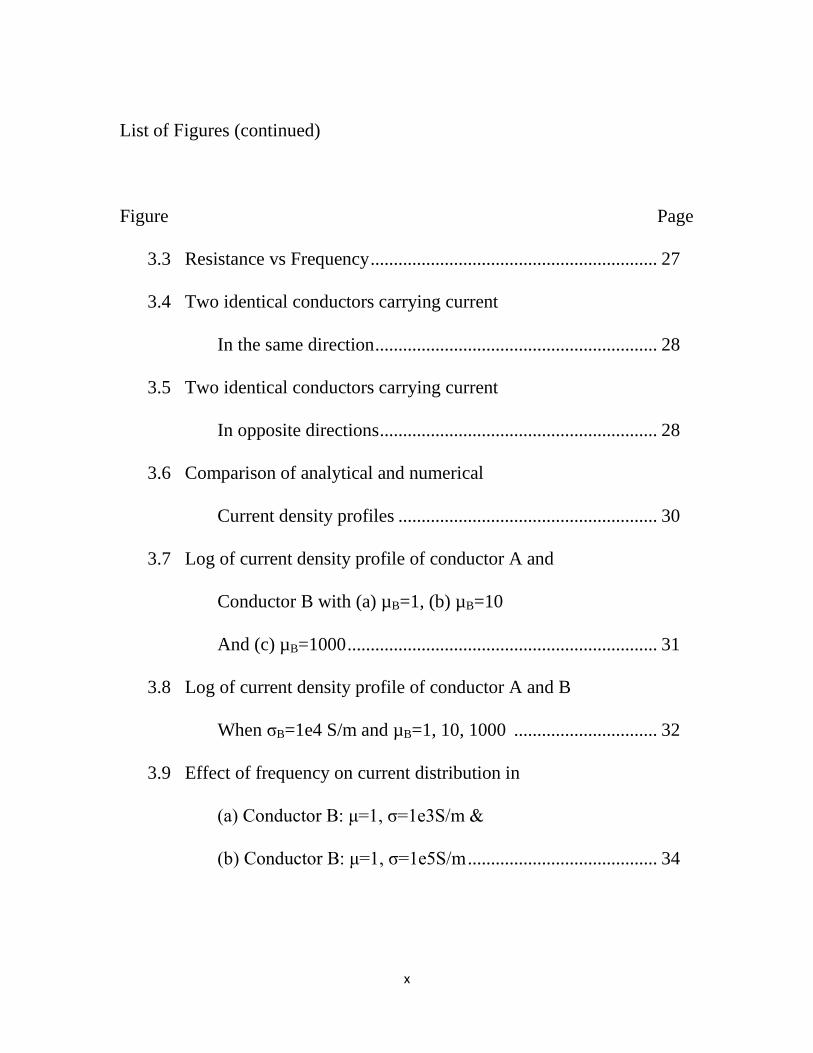
List of Figures (continued)
Figure Page
3.3 Resistance vs Frequency .............................................................. 27
3.4 Two identical conductors carrying current
In the same direction ............................................................. 28
3.5 Two identical conductors carrying current
In opposite directions ............................................................ 28
3.6 Comparison of analytical and numerical
Current density profiles ........................................................ 30
3.7 Log of current density profile of conductor A and
Conductor B with (a) µB=1, (b) µB=10
And (c) µB=1000 ................................................................... 31
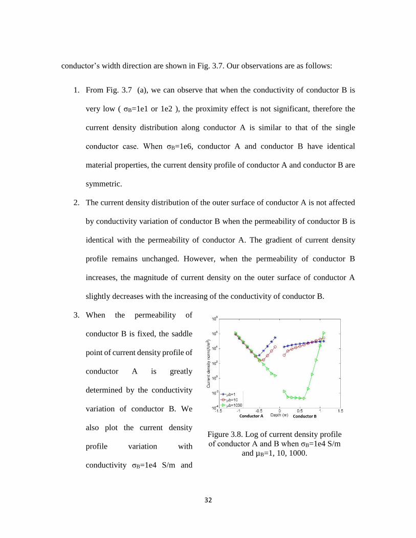
3.8 Log of current density profile of conductor A and B
When σB=1e4 S/m and µB=1, 10, 1000 ............................... 32
3.9 Effect of frequency on current distribution in
(a) Conductor B: μ=1, σ=1e3S/m &
(b) Conductor B: μ=1, σ=1e5S/m ......................................... 34
xi
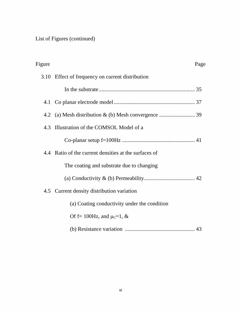
List of Figures (continued)
Figure Page
3.10 Effect of frequency on current distribution
In the substrate ...................................................................... 35
4.1 Co planar electrode model ........................................................... 37
4.2 (a) Mesh distribution & (b) Mesh convergence .......................... 39
4.3 Illustration of the COMSOL Model of a
Co-planar setup f=100Hz ..................................................... 41
4.4 Ratio of the current densities at the surfaces of
The coating and substrate due to changing
(a) Conductivity & (b) Permeability ..................................... 42
4.5 Current density distribution variation
(a) Coating conductivity under the condition
Of f= 100Hz, and μC=1, &
(b) Resistance variation ................................................... 43
xii
List of Figures (continued)
Figure Page
4.6 Current density distribution with depth at different
AC frequency and resistance variation with
Frequency (a, c) μC=1, σC=1e3 S/m, &
(b, d) μC=5, σC=1e3S/m ................................................... 44
4.7 Surface and Interface current densities variation with
Coating conductivity for
(a) μC =1, and (b) μC =5 ................................................ 45
5.1 Mesh around the crack ................................................................ 49
5.2 COMSOL model representing current flow around a
Coating crack at 1000Hz ............................................ 50
5.3 Current density distribution for a frequency
Of 100Hz, μ=1 ............................................................. 52
5.4 Current density distribution for a frequency
Of 1000Hz, μ=5 ..................................................................... 52
xiii
List of Figures (continued)
Figure Page
5.5 Change in
(a) Absolute resistances due to a coating crack, &
(b) Resistance sensitivity due to a coating crack ................... 53
5.6 COMSOL model representing current flow around
An interface crack at 100Hz .................................................. 54
5.7 Current density distribution for a frequency
Of 100Hz, μ=1 ........................................................................ 55
5.8 Current density distribution for a frequency
Of 1000Hz, μ=5 ...................................................................... 55
5.9a Change in resistance versus Conductivity
At F=1e8Hz............................................................................. 57
5.9b Change in reactance versus Conductivity
At F=1e8Hz............................................................................. 57
1
CHAPTER 1. BACKGROUND AND MOTIVATION
1.1 Non-Destructive Testing and Evaluation
Non-destructive testing (NDT) is a broad, interdisciplinary field, which plays a
critical role in assuring that structural components and systems perform their function in a
reliable and cost effective fashion. The tests are performed in a manner that does not affect
the future usefulness of the structural components. In other words, NDT allows structural
components to be inspected and measured without damaging them. Therefore, NDT
provides an excellent balance between quality control and cost-effectiveness [1, 2, 3, 4, 5,
6]. Non-destructive evaluation (NDE) is a term that is used to describe measurements that
are more quantitative in nature. For example, an NDE method would not only locate a
defect, but also measure the size, shape and orientation of the defect. NDE can also be
adopted to determine material properties such as fracture toughness, formability and other
physical characteristics [1].
A brief description of the most popular types of NDT methods is listed below [1,
4, 5, 6].
Visual testing (VT) – the most basic method of NDT is visual examination. Visual
examiners follow procedures that range from simply looking at a part to see if surface
imperfections are visible, to using computer controlled camera systems to automatically
recognize and measure features of a component. This method is typically adopted to detect
2
corrosion, misalignment of parts and possible damage to the material without too much
cost. However, it cannot be used very effectively to detect hidden flaws in the material.
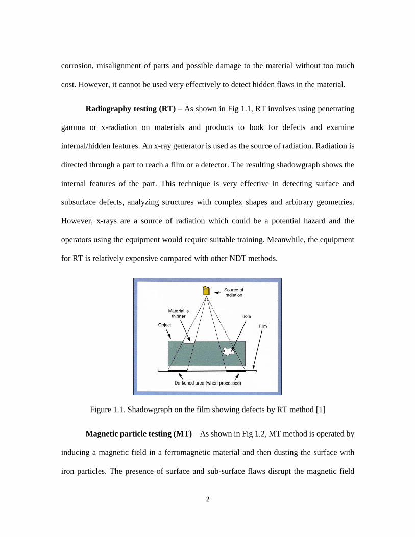
Radiography testing (RT) – As shown in Fig 1.1, RT involves using penetrating
gamma or x-radiation on materials and products to look for defects and examine
internal/hidden features. An x-ray generator is used as the source of radiation. Radiation is
directed through a part to reach a film or a detector. The resulting shadowgraph shows the
internal features of the part. This technique is very effective in detecting surface and
subsurface defects, analyzing structures with complex shapes and arbitrary geometries.
However, x-rays are a source of radiation which could be a potential hazard and the
operators using the equipment would require suitable training. Meanwhile, the equipment
for RT is relatively expensive compared with other NDT methods.
Figure 1.1. Shadowgraph on the film showing defects by RT method [1]
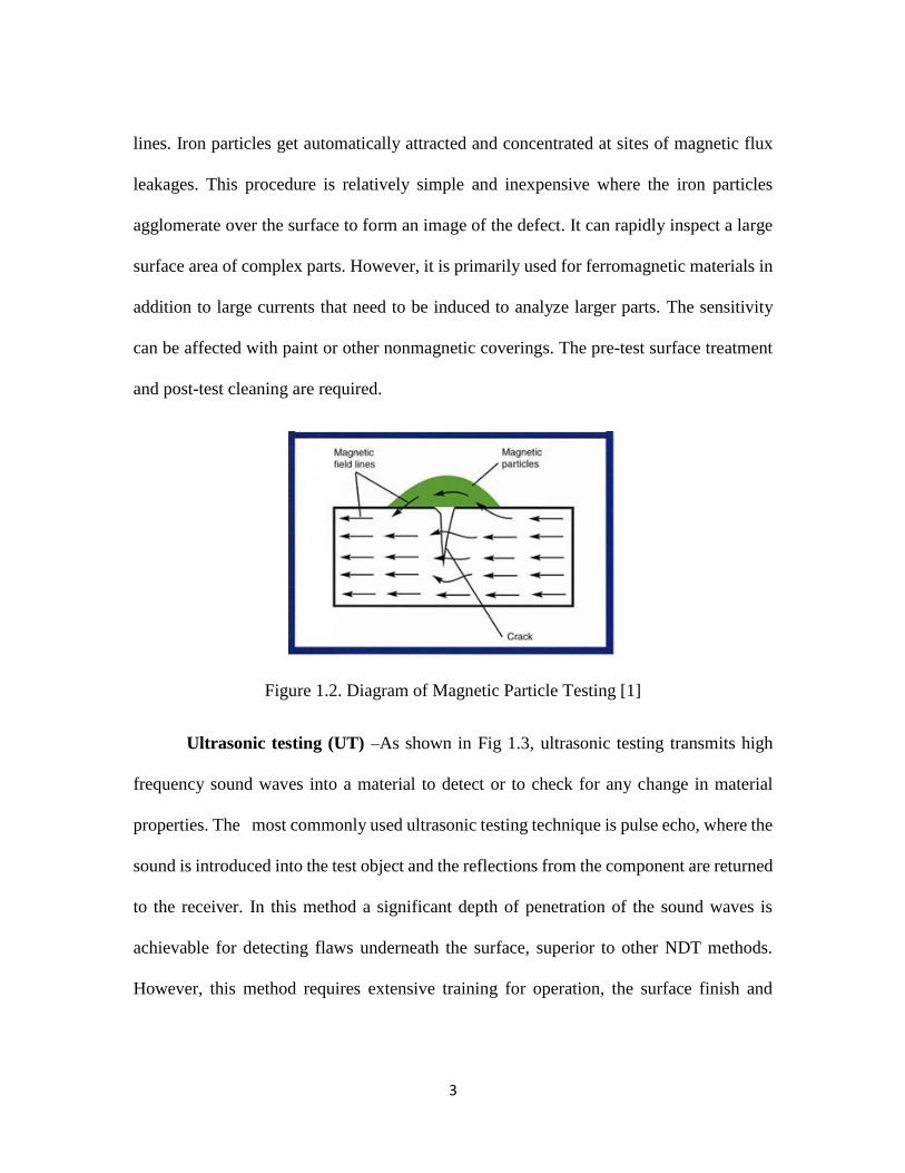
Magnetic particle testing (MT) – As shown in Fig 1.2, MT method is operated by
inducing a magnetic field in a ferromagnetic material and then dusting the surface with
iron particles. The presence of surface and sub-surface flaws disrupt the magnetic field
3
lines. Iron particles get automatically attracted and concentrated at sites of magnetic flux
leakages. This procedure is relatively simple and inexpensive where the iron particles
agglomerate over the surface to form an image of the defect. It can rapidly inspect a large
surface area of complex parts. However, it is primarily used for ferromagnetic materials in
addition to large currents that need to be induced to analyze larger parts. The sensitivity
can be affected with paint or other nonmagnetic coverings. The pre-test surface treatment
and post-test cleaning are required.
Figure 1.2. Diagram of Magnetic Particle Testing [1]
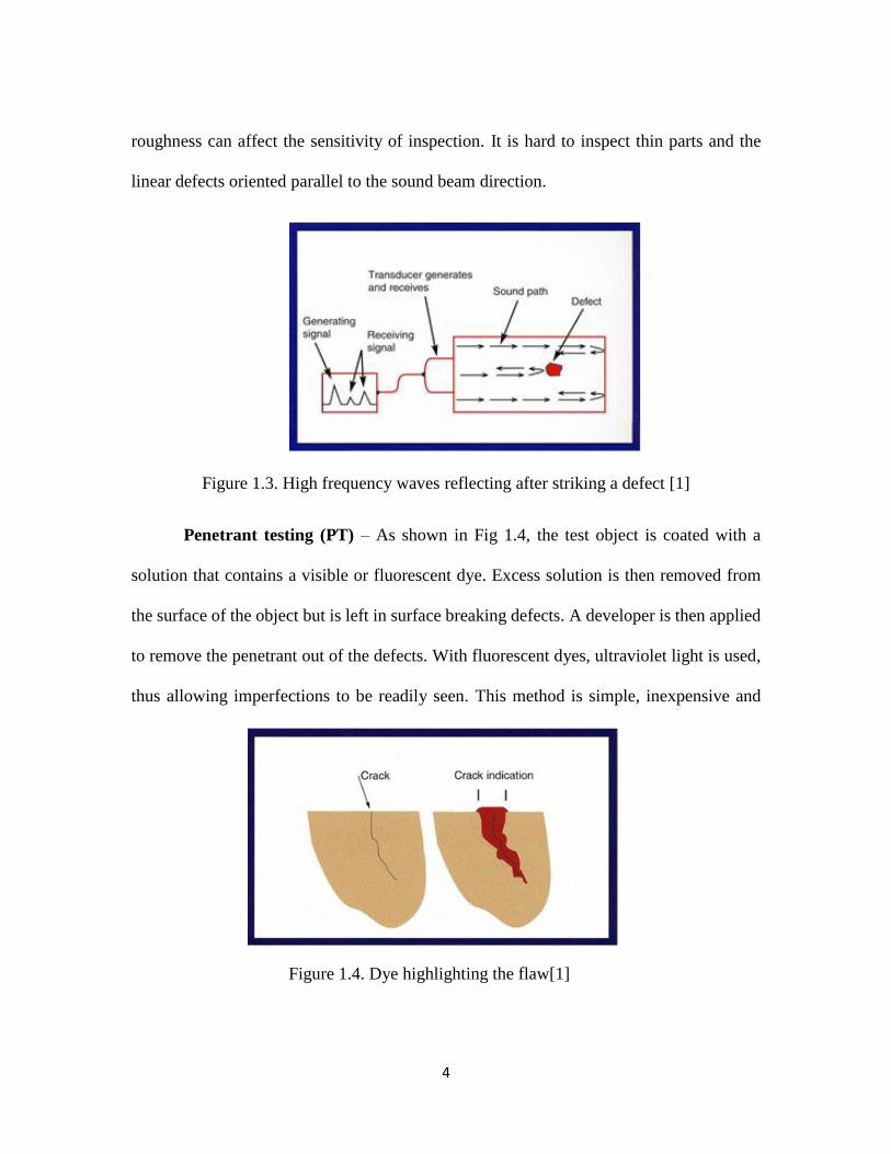
Ultrasonic testing (UT) –As shown in Fig 1.3, ultrasonic testing transmits high
frequency sound waves into a material to detect or to check for any change in material
properties. The most commonly used ultrasonic testing technique is pulse echo, where the
sound is introduced into the test object and the reflections from the component are returned
to the receiver. In this method a significant depth of penetration of the sound waves is
achievable for detecting flaws underneath the surface, superior to other NDT methods.
However, this method requires extensive training for operation, the surface finish and
4
roughness can affect the sensitivity of inspection. It is hard to inspect thin parts and the
linear defects oriented parallel to the sound beam direction.
Figure 1.3. High frequency waves reflecting after striking a defect [1]
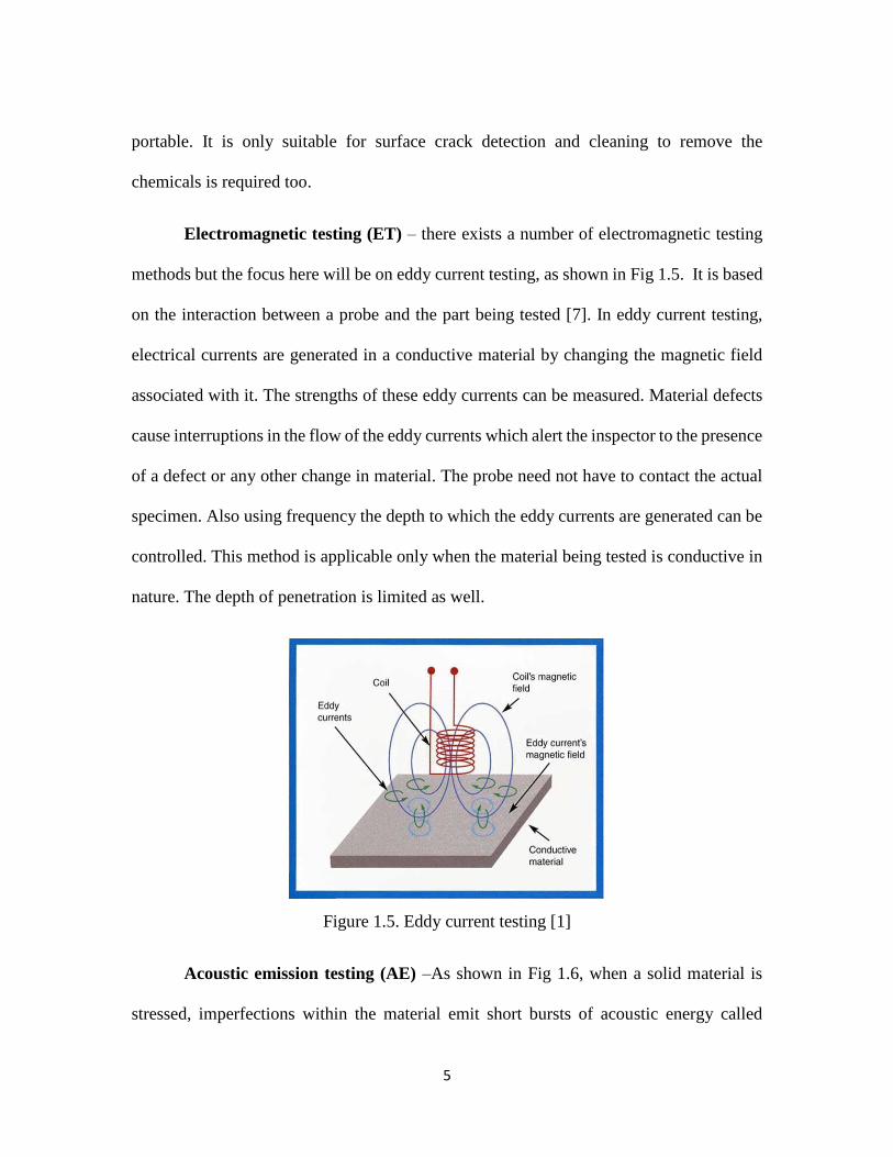
Penetrant testing (PT) – As shown in Fig 1.4, the test object is coated with a
solution that contains a visible or fluorescent dye. Excess solution is then removed from
the surface of the object but is left in surface breaking defects. A developer is then applied
to remove the penetrant out of the defects. With fluorescent dyes, ultraviolet light is used,
thus allowing imperfections to be readily seen. This method is simple, inexpensive and
Figure 1.4. Dye highlighting the flaw[1]
5
portable. It is only suitable for surface crack detection and cleaning to remove the
chemicals is required too.
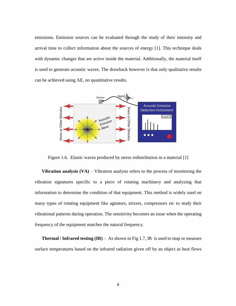
Electromagnetic testing (ET) – there exists a number of electromagnetic testing
methods but the focus here will be on eddy current testing, as shown in Fig 1.5. It is based
on the interaction between a probe and the part being tested [7]. In eddy current testing,
electrical currents are generated in a conductive material by changing the magnetic field
associated with it. The strengths of these eddy currents can be measured. Material defects
cause interruptions in the flow of the eddy currents which alert the inspector to the presence
of a defect or any other change in material. The probe need not have to contact the actual
specimen. Also using frequency the depth to which the eddy currents are generated can be
controlled. This method is applicable only when the material being tested is conductive in
nature. The depth of penetration is limited as well.
Figure 1.5. Eddy current testing [1]
Acoustic emission testing (AE) –As shown in Fig 1.6, when a solid material is
stressed, imperfections within the material emit short bursts of acoustic energy called
6
emissions. Emission sources can be evaluated through the study of their intensity and
arrival time to collect information about the sources of energy [1]. This technique deals
with dynamic changes that are active inside the material. Additionally, the material itself
is used to generate acoustic waves. The drawback however is that only qualitative results
can be achieved using AE, no quantitative results.
Figure 1.6. Elastic waves produced by stress redistribution in a material [1]
Vibration analysis (VA) – Vibration analysis refers to the process of monitoring the
vibration signatures specific to a piece of rotating machinery and analyzing that
information to determine the condition of that equipment. This method is widely used on
many types of rotating equipment like agitators, mixers, compressors etc to study their
vibrational patterns during operation. The sensitivity becomes an issue when the operating
frequency of the equipment matches the natural frequency.
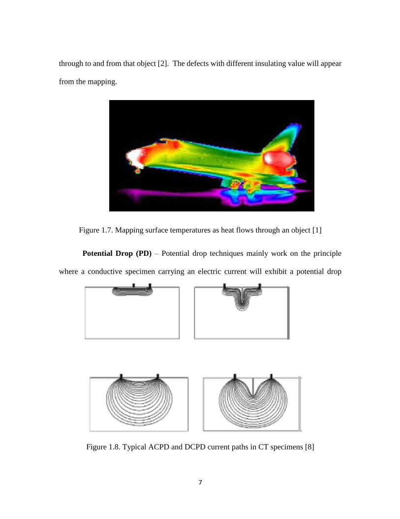
Thermal / Infrared testing (IR) – As shown in Fig 1.7, IR is used to map or measure
surface temperatures based on the infrared radiation given off by an object as heat flows
7
through to and from that object [2]. The defects with different insulating value will appear
from the mapping.
Figure 1.7. Mapping surface temperatures as heat flows through an object [1]
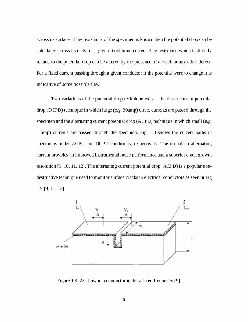
Potential Drop (PD) – Potential drop techniques mainly work on the principle
where a conductive specimen carrying an electric current will exhibit a potential drop
Figure 1.8. Typical ACPD and DCPD current paths in CT specimens [8]
8
across its surface. If the resistance of the specimen is known then the potential drop can be
calculated across its ends for a given fixed input current. The resistance which is directly
related to the potential drop can be altered by the presence of a crack or any other defect.
For a fixed current passing through a given conductor if the potential were to change it is
indicative of some possible flaw.
Two variations of the potential drop technique exist – the direct current potential
drop (DCPD) technique in which large (e.g. 30amp) direct currents are passed through the
specimen and the alternating current potential drop (ACPD) technique in which small (e.g.
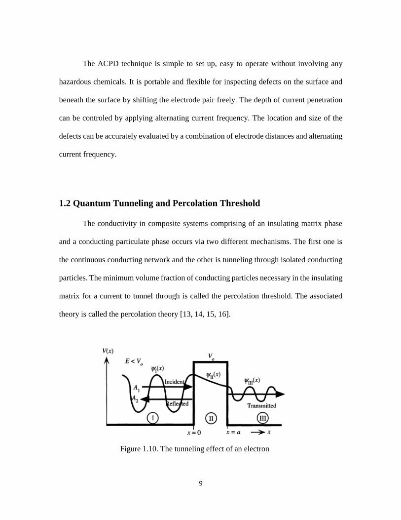
1 amp) currents are passed through the specimen. Fig. 1.8 shows the current paths in
specimens under ACPD and DCPD conditions, respectively. The use of an alternating
current provides an improved instrumental noise performance and a superior crack growth
resolution [9, 10, 11, 12]. The alternating current potential drop (ACPD) is a popular non-
destructive technique used to monitor surface cracks in electrical conductors as seen in Fig
1.9 [9, 11, 12].
Figure 1.9. AC flow in a conductor under a fixed frequency [9]
9
The ACPD technique is simple to set up, easy to operate without involving any
hazardous chemicals. It is portable and flexible for inspecting defects on the surface and
beneath the surface by shifting the electrode pair freely. The depth of current penetration
can be controled by applying alternating current frequency. The location and size of the
defects can be accurately evaluated by a combination of electrode distances and alternating
current frequency.
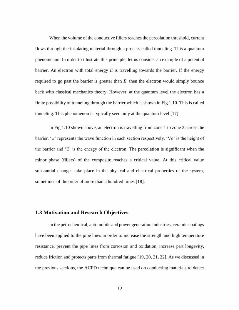
1.2 Quantum Tunneling and Percolation Threshold
The conductivity in composite systems comprising of an insulating matrix phase
and a conducting particulate phase occurs via two different mechanisms. The first one is
the continuous conducting network and the other is tunneling through isolated conducting
particles. The minimum volume fraction of conducting particles necessary in the insulating
matrix for a current to tunnel through is called the percolation threshold. The associated
theory is called the percolation theory [13, 14, 15, 16].
Figure 1.10. The tunneling effect of an electron
10
When the volume of the conductive fillers reaches the percolation threshold, current
flows through the insulating material through a process called tunneling. This a quantum
phenomenon. In order to illustrate this principle, let us consider an example of a potential
barrier. An electron with total energy E is travelling towards the barrier. If the energy
required to go past the barrier is greater than E, then the electron would simply bounce
back with classical mechanics theory. However, at the quantum level the electron has a
finite possibility of tunneling through the barrier which is shown in Fig 1.10. This is called
tunneling. This phenomenon is typically seen only at the quantum level [17].
In Fig 1.10 shown above, an electron is travelling from zone 1 to zone 3 across the
barrier. ‘ψ’ represents the wave function in each section respectively. ‘Vo’ is the height of
the barrier and ‘E’ is the energy of the electron. The percolation is significant when the
minor phase (fillers) of the composite reaches a critical value. At this critical value
substantial changes take place in the physical and electrical properties of the system,
sometimes of the order of more than a hundred times [18].
1.3 Motivation and Research Objectives
In the petrochemical, automobile and power generation industries, ceramic coatings
have been applied to the pipe lines in order to increase the strength and high temperature
resistance, prevent the pipe lines from corrosion and oxidation, increase part longevity,
reduce friction and protects parts from thermal fatigue [19, 20, 21, 22]. As we discussed in
the previous sections, the ACPD technique can be used on conducting materials to detect
11
surface cracks and subsurface cracks by injecting an alternating current and detecting the
potential drop due to the defects. It is portable, easy to operate, hazardless, and flexible by
shifting the sensing electrodes across the surface. Therefore, the ACPD method is the most
popular NDT method to be adopted to detect cracks for metal pipelines which are
electrically conductive.
However, most of the ceramic coating material for metal pipelines are electrically
insulating, which limits the usage of the ACPD method. In order to overcome this
difficulty, we proposed a concept of a multi-functional ceramic coating material, in which
the metal nanoparticles (such as Nickel) can be uniformly embedded into the ceramic
matrix (mullite). This multi-functional ceramic matrix nanocomposite developed in
Dr. Peng’s lab can conduct current via tunneling when the percolation threshold is reached.
Therefore, this multi-functional ceramic coating can not only keep the advantages of
traditional ceramics coating, but also allow the capability of ACPD technique for NDT
evaluation. The research objectives of this study has three folds. (1) Understanding the
ACPD technique; (2) evaluate the relation between signal sensitivity and coating material
properties; and (3) evaluate the signal sensitivity under the condition of surface/interface
cracks. In the following chapters, we will first introduce the fundamental physics related
with ACPD technique and numerical simulation set up(Chapter 2); then we will investigate
the ACPD technique through the two parallel conductor case (Chapter 3) and co-planar
coating-substrate case (Chapter 4). We will further investigate the signal sensitivity of
crack detection under the coating-substrate setup (Chapter 5) and draw conclusions in the
end (Chapter 6).
12
CHAPTER 2. RESEARCH METHOD
2.1 Introduction to Electromagnetics
The fundamental physics behind the ACPD method is the electro-magnetic field
coupling. The magnetic field generated by the injected AC current will cause the current
density redistribution within the domain. In DC circuits, the relation between voltage V,
current I and resistance R is V=I∙R. In AC circuits, two additional impeding mechanisms
are taken into account, which are the induction of voltages in conductors self-induced by
the magnetic field of current (inductance), and the electrostatic storage of charge induced
by voltages between conductors (capacitance) [23]. Therefore, the concept of impedance
Z is introduced with the real part R corresponding to the resistance, and the imaginary part
L corresponding to the inductance or simply the effective reactance, as shown in Eq. (2.1).
, iV
Z Z R LI
(2.1)
The basic laws associated with electromagnetics include: [24]
Ampere’s law – it describes the relationship between the current and magnetic field
produced by the current itself. It states that the closed line integral of the magnetic
field intensity H around a closed path is equal to the total current I enclosed by the
path, and passing through the inside of the conductor.
13
Faradays law – it states that a changing current in one wire causes a changing
magnetic field that induces a current in the opposite direction in another close by
wire.
Gauss’s Law – it is the law related with electric charge distribution and the
resulting electric field, by which the net electric flux through any closed surface is
equal to 1/ε times the net electric charge enclosed within that closed surface, where
ε is the electric constant.
Gauss’s magnetic law - It states that the magnetic field B has divergence equal to
zero.
The electromagnetic theory can be described with the set of Maxwell’s equation [24]. The
microscopic (differential) form of Maxwell’s equations at a point in space are given by,
Ampere’s law, ∇ × 𝐻 = 𝐽 + 𝜕𝐷
𝜕𝑡= 𝜎𝐸 + 휀
𝜕𝐸
𝜕𝑡 (2.2)
Faraday’s law, ∇ × 𝐸 = −𝜕𝐵
𝜕𝑡= −µ
𝜕𝐻
𝜕𝑡 (2.3)
Gauss’s law, ∇ ∙ 𝐸 = 𝜌/휀0 (2.4)
Gauss’s magnetic law, ∇ ∙ 𝐵 = 0 (2.5)
Where, J is the current charge density, E is the electric field intensity, 휀0 is the electric
constant, H is the magnetic field intensity, B magnetic flux density and ρ is the electric
charge density.
The law of conservation of charge or the continuity equation must be satisfied at all times.
It is given by
14
∇ . 𝐽 = −𝜕𝜌
𝜕𝑡 (2.6)
The law states that the time rate of change of electric charge ρ is a source of electric
current density field J. This means that the current density is continuous and charge can
only be transferred, neither be created nor destroyed.
The Maxwell’s equations are derived by making use of a set of constitutive relations,
B = µ H (2.7)
D = ε E (2.8)
J = σ E (2.9)
Where, σ is the electrical conductivity, ε is the dielectric permittivity and μ is the magnetic
permeability.
Based on Faraday’s law, any time varying magnetic field will produce an electric
field. The currents produced by the time varying magnetic field are called the Eddy
Currents. There are primarily two types of eddy current effects – the skin effect and the
proximity effect.
2.1.1 Skin Effect
When a conductor is carrying an AC current, it will produce a magnetic field inside
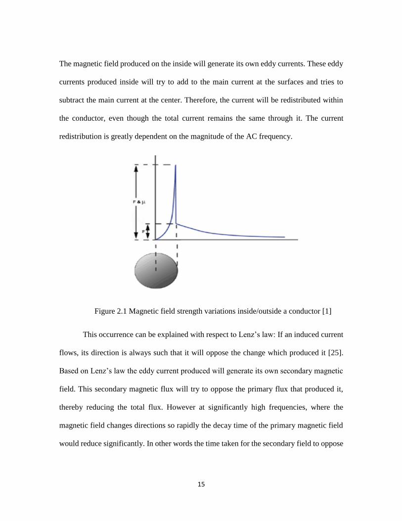
and around the conductor. Inside the conductor the magnetic field strength increases from
the center to the surface as shown in Fig 2.1. Outside the conductor the magnetic field
strength decreases as an inverse relation with respect to the distance from the outer surface.
15
The magnetic field produced on the inside will generate its own eddy currents. These eddy
currents produced inside will try to add to the main current at the surfaces and tries to
subtract the main current at the center. Therefore, the current will be redistributed within
the conductor, even though the total current remains the same through it. The current
redistribution is greatly dependent on the magnitude of the AC frequency.
Figure 2.1 Magnetic field strength variations inside/outside a conductor [1]
This occurrence can be explained with respect to Lenz’s law: If an induced current
flows, its direction is always such that it will oppose the change which produced it [25].
Based on Lenz’s law the eddy current produced will generate its own secondary magnetic
field. This secondary magnetic flux will try to oppose the primary flux that produced it,
thereby reducing the total flux. However at significantly high frequencies, where the
magnetic field changes directions so rapidly the decay time of the primary magnetic field
would reduce significantly. In other words the time taken for the secondary field to oppose
16
the primary field is cut down at high frequencies, owing to which the current distribution
stays more non-uniform. At lower frequencies however, the secondary field would get
significantly more time to disintegrate the primary flux. This means it would try to restore
the current distribution to its uniform pattern. At very high frequencies the whole current
in the conductor would try to flow along the surface. This is termed as the skin effect,
where the entire current is trying to flow in a thin skin-like layer [24]. The part can be
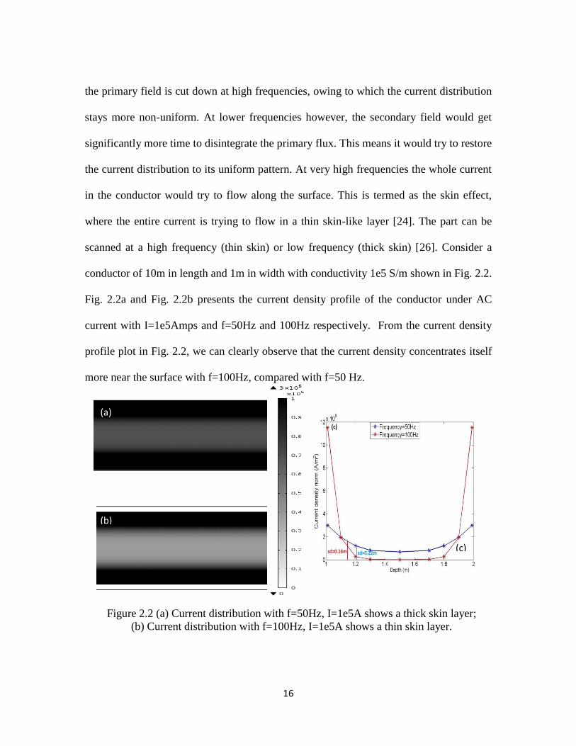
scanned at a high frequency (thin skin) or low frequency (thick skin) [26]. Consider a
conductor of 10m in length and 1m in width with conductivity 1e5 S/m shown in Fig. 2.2.
Fig. 2.2a and Fig. 2.2b presents the current density profile of the conductor under AC
current with I=1e5Amps and f=50Hz and 100Hz respectively. From the current density
profile plot in Fig. 2.2, we can clearly observe that the current density concentrates itself
more near the surface with f=100Hz, compared with f=50 Hz.
Figure 2.2 (a) Current distribution with f=50Hz, I=1e5A shows a thick skin layer;
(b) Current distribution with f=100Hz, I=1e5A shows a thin skin layer.
(a)
(b)
(c)
17
The skin effect causes high frequency current to flow at the surface of the conductor
and it decays as an exponential function towards the conductor’s center. The skin depth
may be defined as the depth from the surface to which about 67% of the current flows.
Alternatively, it may be described in terms of current density at a point in the conductor at
which the current density is about 1/e times its current density at the surface. The skin depth
is inversely related to the square root of frequency given by [27]
𝛿 = √1
𝜋𝑓𝜇𝜎 (2.10)
Where δ is the skin depth, f is the applied frequency, μ is the magnetic permeability and σ
is the electrical conductivity.
The current density profile defined by surface current density and skin depth is given by,
[28]
𝐽(𝑥) = 𝐽𝑜 𝑒−𝑑
𝛿 (2.11)
Where J(x) is the current density at a point from the surface, Jo is the current density at the
surface, d is the distance from the surface towards the center and δ is the skin depth.
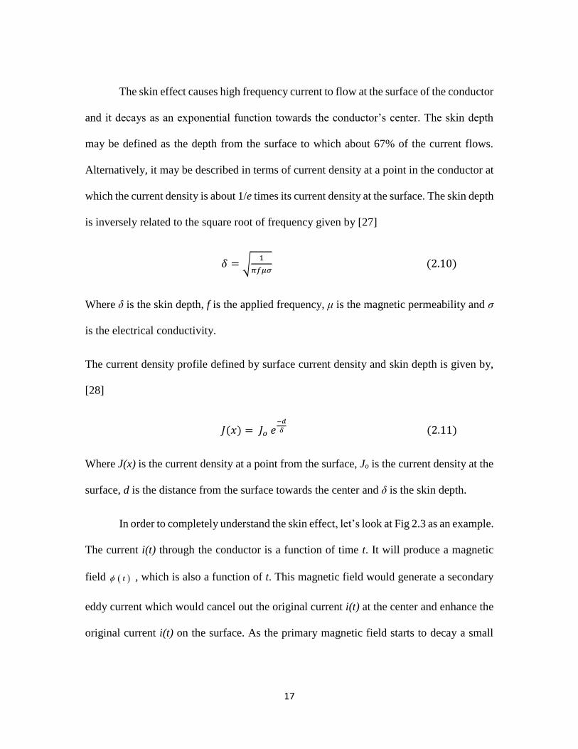
In order to completely understand the skin effect, let’s look at Fig 2.3 as an example.
The current i(t) through the conductor is a function of time t. It will produce a magnetic
field t , which is also a function of t. This magnetic field would generate a secondary
eddy current which would cancel out the original current i(t) at the center and enhance the
original current i(t) on the surface. As the primary magnetic field starts to decay a small
18
portion of the current would try to flow through. As this decay of the primary field increases
more current flows through, and continues until all the main current flows uniformly across
the whole conductor. But, if this process of current regeneration were to be interrupted
every time the full decay would never occur. As a result the effect of the primary field will
dominate, because the secondary magnetic flux cannot get sufficient time to oppose the
main flux. Every time the current reverses direction at some frequency, the process is
repeated again. This continued decay and build up depending on the frequency level causes
current to flow in a restricted region of the conductor non-uniformly.
.
Figure 2.3. Eddy currents produced due to the changing magnetic field direction [29]
Fig 2.4 represents the current distribution along the radius direction of the
conductor under the AC and DC, respectively. With DC, the current distribution along the
radius direction of the conductor is constant, as the green solid line shown. With AC, the
current is redistributed due to the eddy current effect, as by blue solid line shown. The
current density is much higher near the surface of the conductor and vanishes when
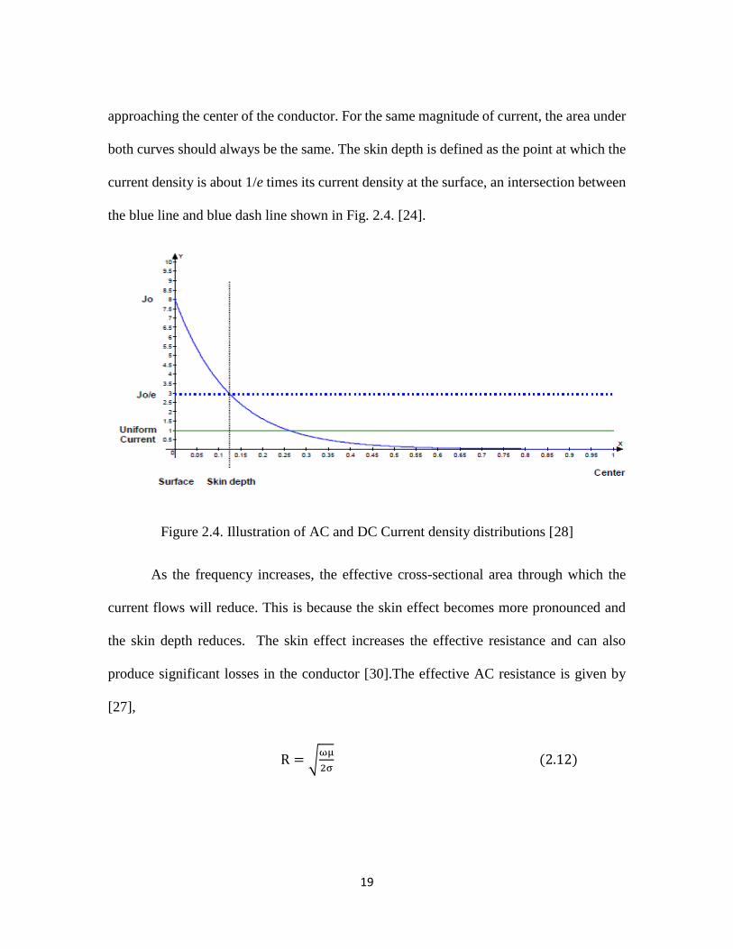
19
approaching the center of the conductor. For the same magnitude of current, the area under
both curves should always be the same. The skin depth is defined as the point at which the
current density is about 1/e times its current density at the surface, an intersection between
the blue line and blue dash line shown in Fig. 2.4. [24].
Figure 2.4. Illustration of AC and DC Current density distributions [28]
As the frequency increases, the effective cross-sectional area through which the
current flows will reduce. This is because the skin effect becomes more pronounced and
the skin depth reduces. The skin effect increases the effective resistance and can also
produce significant losses in the conductor [30].The effective AC resistance is given by
[27],
R = √ωμ
2σ (2.12)
20
Where R is the effective resistance, σ is the electrical conductivity, μ is the magnetic
permeability and ω is the angular frequency.
As seen from the above relation, the resistance of the conductor is related to the inverse
square root of frequency, and the material properties of the conductor.
2.1.2 Proximity Effect
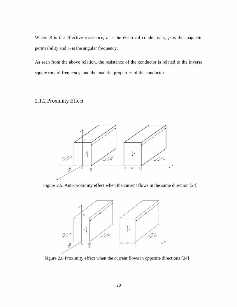
Figure 2.5. Anti-proximity effect when the current flows in the same direction [24]
Figure 2.6 Proximity effect when the current flows in opposite directions [24]

21
The redistribution of current in a single conductor due to the alternative current is
defined as skin effect. When another conductor is brought in the vicinity of the primary
current carrying conductor, the effect of the magnetic field to the current distribution is
different. The magnetic field produced externally by the primary conductor cuts the
secondary conductor, producing eddy currents in it. The eddy currents produced in the
second conductor’s face closer to the first conductor oppose the primary current and the
eddy current produced on the farther face will add to the main current, as shown in Fig.
2.5. This actually is termed as the anti-proximity effect and occurs when the current flow
is in the same direction in both conductors. When the current flow in each conductor is in
opposite directions, the eddy currents will add at the center and oppose at the end faces, as
shown in Fig. 2.6. This is called the proximity effect [24].
The proximity effect results in a non-uniform current distribution. Both skin and
proximity effect cause a significant redistribution of current in the conductor. The
magnitude of the proximity effect depends upon the following factors [24],
Alternating current frequency
Conductor geometry
Arrangement of conductors
Spacing
The proximity effect further increases the effective AC resistance when compared
to DC. The impedance in each plate is given by [24],
𝑍 = 𝐹𝑟 + 𝑗(𝐹𝑥) (2.13)
22
Where Fx is the normalized reactance and Fr is the resistance factor given by,
𝐹𝑟 =𝑤
𝛿.
sinh2𝑤𝛿
+ sin2𝑤𝛿
cosh2𝑤𝛿
− cos2𝑤𝛿
(2.14)
Where, w is the plate width and δ is the skin depth.
The skin and proximity effects can also be calculated separately due to the
orthogonal nature between them. The phase of the total current density can be expressed
as the sum of the skin current density Js and the proximity current density Jp. If the
conductor has an axis of symmetry and the applied field is uniform and parallel to the axis
of symmetry, the distribution of skin current density is an even function and the distribution
of the proximity current density is an odd function [31].
2.2 Numerical Simulation Method
In this study, we employ the finite element software COMSOL Multiphysics 4.4
[32] to conduct our investigation. As a multi-physics platform, COMSOL offers several
modules and interfaces for electronic-magnetic coupling problems. To achieve our goal,
we adopted the “magnetic and electric field (mef)” interface within the “AC/DC” module
with the setup details as follows.
1) We investigate a two dimensional domain with a finite depth in the out of plane
direction.
23
2) We assume the multi-functional ceramic coating has uniformly low conductivity
without considering the tunneling effect within the domain. Our objective at this
stage is to investigate the effect of low conductivity coating material to the
sensitivity of ACPD technique.
3) The boundary conditions used are as follows – An alternating current of 1e5 Amps
is supplied to one electrode (terminal) and the other electrode is left alone. In
addition, the magnetic insulation boundary condition is applied across all the
exterior boundaries. The electric insulation boundary condition is applied across all
exterior boundaries except for the electrodes.
4) Since the current distribution tends to concentrate itself near the surface/interface
with a large gradient, we adopt the 2-D triangular quadratic meshing elements for
better accuracy.
There are primarily two parameters of interest that are investigated from the
numerical simulation. The current density profile and the impedance are two major
parameters that are analyzed. The current density profile will shed light on the effect of the
film over the interface of the substrate. In addition, the impedance is post processed to give
both its real resistive part and its imaginary inductive part. The impedance is studied to
analyze its change when a crack may be present in the film or substrate. The relative change
in impedance is referred to as the sensitivity.
24
CHAPTER 3. PARALLEL CONDUCTOR MODEL
In this study, we adopt the two parallel conductor model to understand the skin
effect, proximity effect, and the effect of the material property variation on current density
distribution.
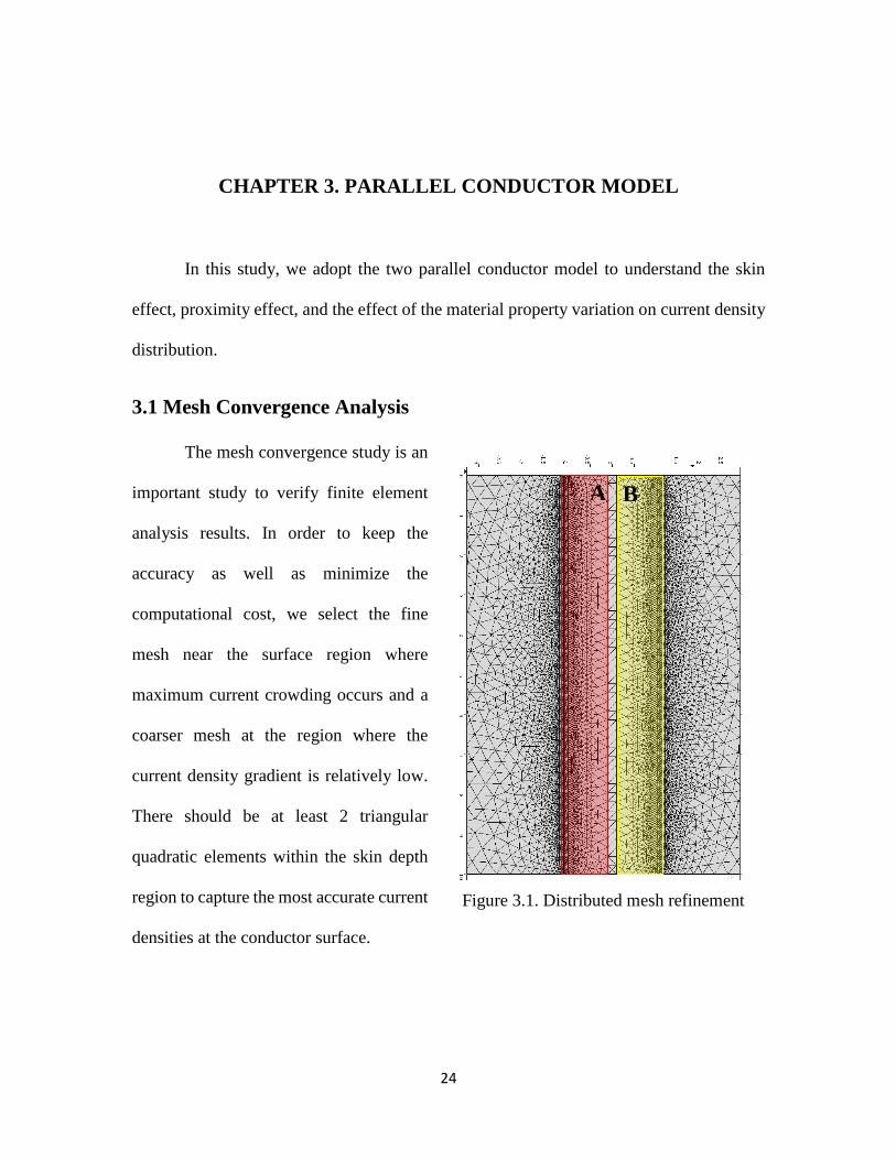
3.1 Mesh Convergence Analysis
The mesh convergence study is an
important study to verify finite element
analysis results. In order to keep the
accuracy as well as minimize the
computational cost, we select the fine
mesh near the surface region where
maximum current crowding occurs and a
coarser mesh at the region where the
current density gradient is relatively low.
There should be at least 2 triangular
quadratic elements within the skin depth
region to capture the most accurate current
densities at the conductor surface.
Figure 3.1. Distributed mesh refinement
A B
25
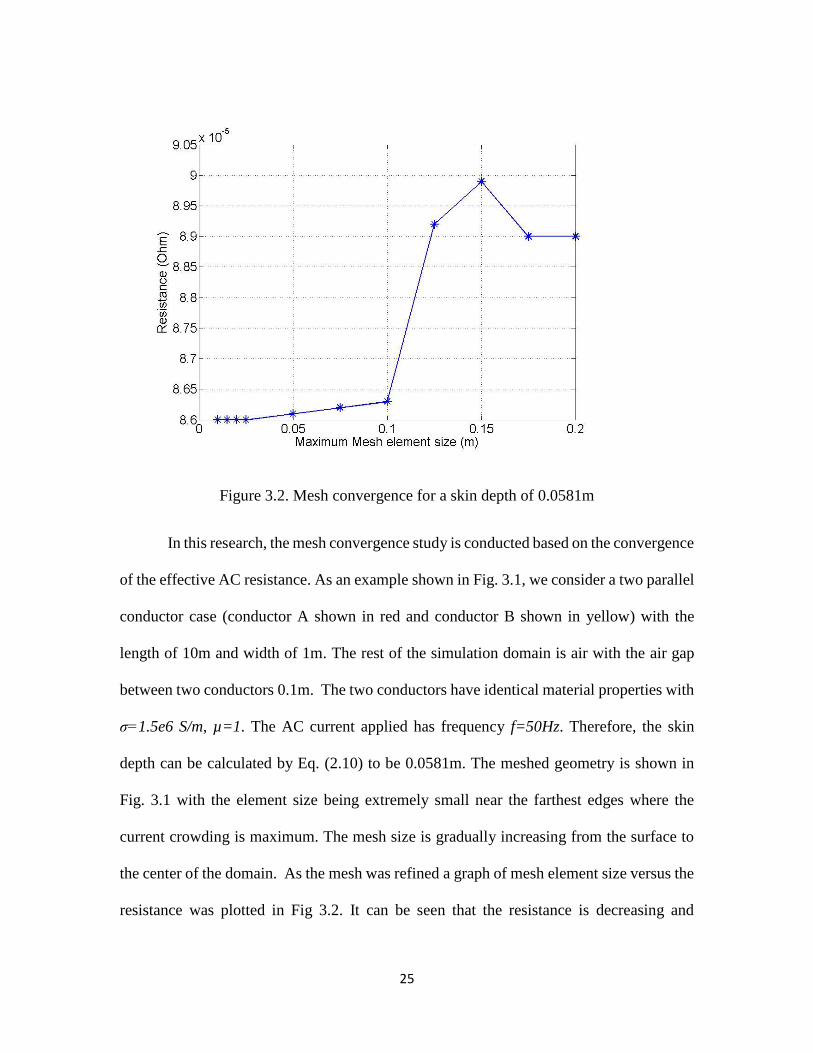
Figure 3.2. Mesh convergence for a skin depth of 0.0581m
In this research, the mesh convergence study is conducted based on the convergence
of the effective AC resistance. As an example shown in Fig. 3.1, we consider a two parallel
conductor case (conductor A shown in red and conductor B shown in yellow) with the
length of 10m and width of 1m. The rest of the simulation domain is air with the air gap
between two conductors 0.1m. The two conductors have identical material properties with
σ=1.5e6 S/m, µ=1. The AC current applied has frequency f=50Hz. Therefore, the skin
depth can be calculated by Eq. (2.10) to be 0.0581m. The meshed geometry is shown in
Fig. 3.1 with the element size being extremely small near the farthest edges where the
current crowding is maximum. The mesh size is gradually increasing from the surface to
the center of the domain. As the mesh was refined a graph of mesh element size versus the
resistance was plotted in Fig 3.2. It can be seen that the resistance is decreasing and
26
converges to a constant value when the element size is less than 0.025m, which is
approximately half the skin depth. In other words two triangular elements within the skin
depth are sufficient to get an accurate enough solution.
Since the skin depth is determined by AC frequency, conductivity and permeability
as shown in Eq (2.10), we found that with the same kind depth, the mesh error induced by
the frequency is greatest when compared to conductivity and permeability. Therefore, in
the following simulations, we perform the mesh convergence study and select the most
reliable mesh for each individual study.
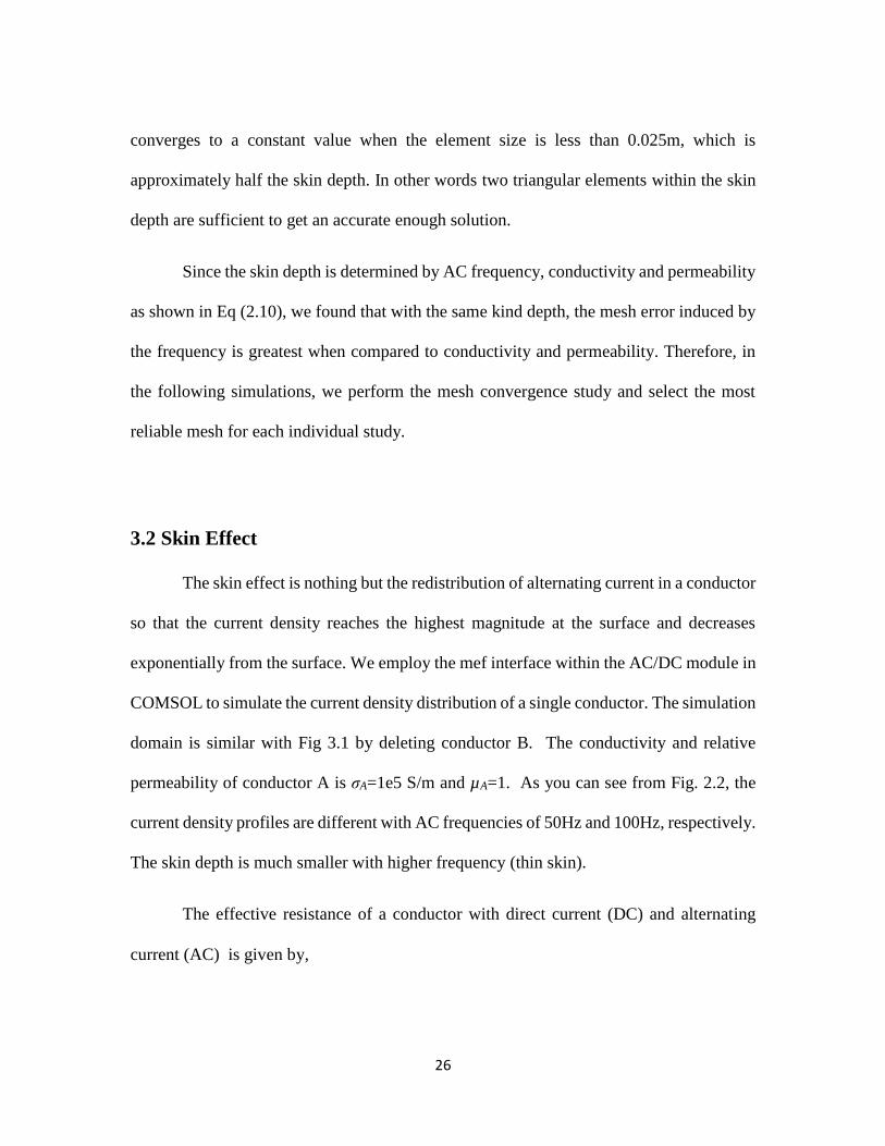
3.2 Skin Effect
The skin effect is nothing but the redistribution of alternating current in a conductor
so that the current density reaches the highest magnitude at the surface and decreases
exponentially from the surface. We employ the mef interface within the AC/DC module in
COMSOL to simulate the current density distribution of a single conductor. The simulation
domain is similar with Fig 3.1 by deleting conductor B. The conductivity and relative
permeability of conductor A is σA=1e5 S/m and µA=1. As you can see from Fig. 2.2, the
current density profiles are different with AC frequencies of 50Hz and 100Hz, respectively.
The skin depth is much smaller with higher frequency (thin skin).
The effective resistance of a conductor with direct current (DC) and alternating
current (AC) is given by,
27
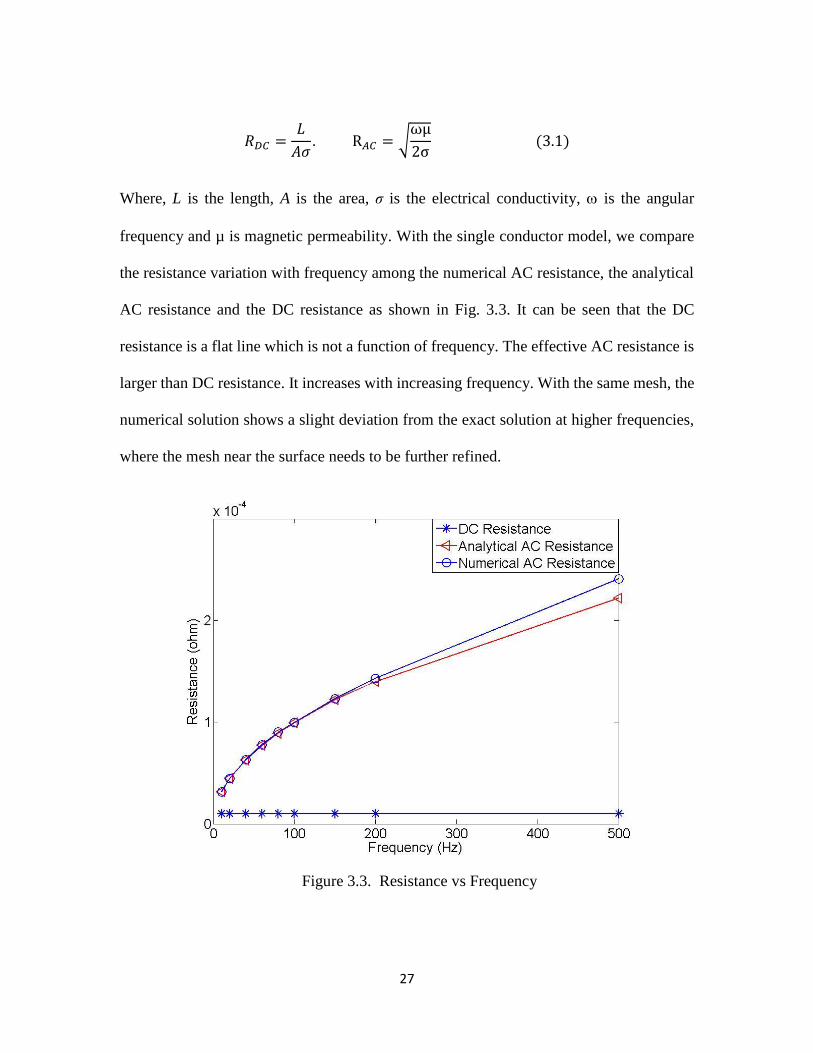
𝑅𝐷𝐶 =𝐿
𝐴𝜎. R𝐴𝐶 = √
ωµ
2σ (3.1)
Where, L is the length, A is the area, σ is the electrical conductivity, is the angular
frequency and µ is magnetic permeability. With the single conductor model, we compare
the resistance variation with frequency among the numerical AC resistance, the analytical
AC resistance and the DC resistance as shown in Fig. 3.3. It can be seen that the DC
resistance is a flat line which is not a function of frequency. The effective AC resistance is
larger than DC resistance. It increases with increasing frequency. With the same mesh, the
numerical solution shows a slight deviation from the exact solution at higher frequencies,
where the mesh near the surface needs to be further refined.
Figure 3.3. Resistance vs Frequency
28
3.3 Proximity Effect
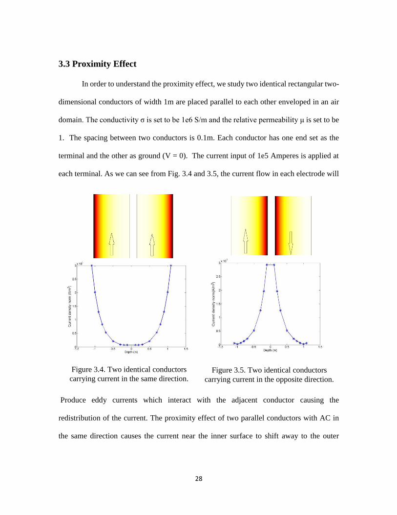
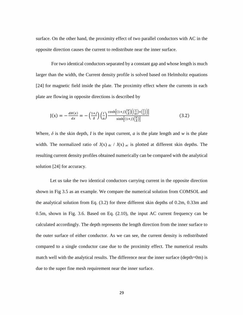
In order to understand the proximity effect, we study two identical rectangular two-
dimensional conductors of width 1m are placed parallel to each other enveloped in an air
domain. The conductivity σ is set to be 1e6 S/m and the relative permeability μ is set to be
1. The spacing between two conductors is 0.1m. Each conductor has one end set as the
terminal and the other as ground (V = 0). The current input of 1e5 Amperes is applied at
each terminal. As we can see from Fig. 3.4 and 3.5, the current flow in each electrode will
Produce eddy currents which interact with the adjacent conductor causing the
redistribution of the current. The proximity effect of two parallel conductors with AC in
the same direction causes the current near the inner surface to shift away to the outer
Figure 3.4. Two identical conductors
carrying current in the same direction. Figure 3.5. Two identical conductors
carrying current in the opposite direction.
29
surface. On the other hand, the proximity effect of two parallel conductors with AC in the
opposite direction causes the current to redistribute near the inner surface.
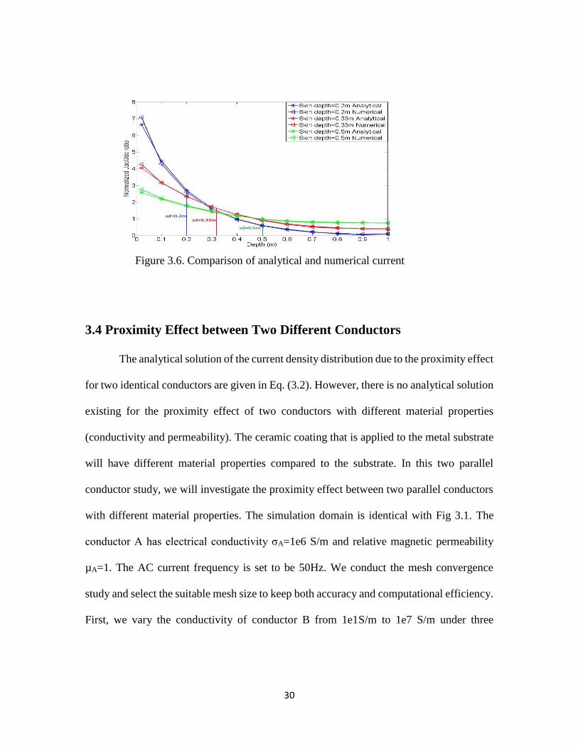
For two identical conductors separated by a constant gap and whose length is much
larger than the width, the Current density profile is solved based on Helmholtz equations
[24] for magnetic field inside the plate. The proximity effect where the currents in each
plate are flowing in opposite directions is described by
J(x) = −𝑑𝐻(𝑥)
𝑑𝑥= − (
1+𝑗
𝛿) (
𝐼
𝑎)
cosh[(1+𝑗)(𝑤
𝛿)((
𝑥
𝑤)+(
1
2))]
sinh[(1+𝑗)(𝑤
𝛿)]
(3.2)
Where, δ is the skin depth, I is the input current, a is the plate length and w is the plate
width. The normalized ratio of J(x) dc / J(x) ac is plotted at different skin depths. The
resulting current density profiles obtained numerically can be compared with the analytical
solution [24] for accuracy.
Let us take the two identical conductors carrying current in the opposite direction
shown in Fig 3.5 as an example. We compare the numerical solution from COMSOL and
the analytical solution from Eq. (3.2) for three different skin depths of 0.2m, 0.33m and
0.5m, shown in Fig. 3.6. Based on Eq. (2.10), the input AC current frequency can be
calculated accordingly. The depth represents the length direction from the inner surface to
the outer surface of either conductor. As we can see, the current density is redistributed
compared to a single conductor case due to the proximity effect. The numerical results
match well with the analytical results. The difference near the inner surface (depth=0m) is
due to the super fine mesh requirement near the inner surface.
30
3.4 Proximity Effect between Two Different Conductors
The analytical solution of the current density distribution due to the proximity effect
for two identical conductors are given in Eq. (3.2). However, there is no analytical solution
existing for the proximity effect of two conductors with different material properties
(conductivity and permeability). The ceramic coating that is applied to the metal substrate
will have different material properties compared to the substrate. In this two parallel
conductor study, we will investigate the proximity effect between two parallel conductors
with different material properties. The simulation domain is identical with Fig 3.1. The
conductor A has electrical conductivity σA=1e6 S/m and relative magnetic permeability
µA=1. The AC current frequency is set to be 50Hz. We conduct the mesh convergence
study and select the suitable mesh size to keep both accuracy and computational efficiency.
First, we vary the conductivity of conductor B from 1e1S/m to 1e7 S/m under three
Figure 3.6. Comparison of analytical and numerical current
31
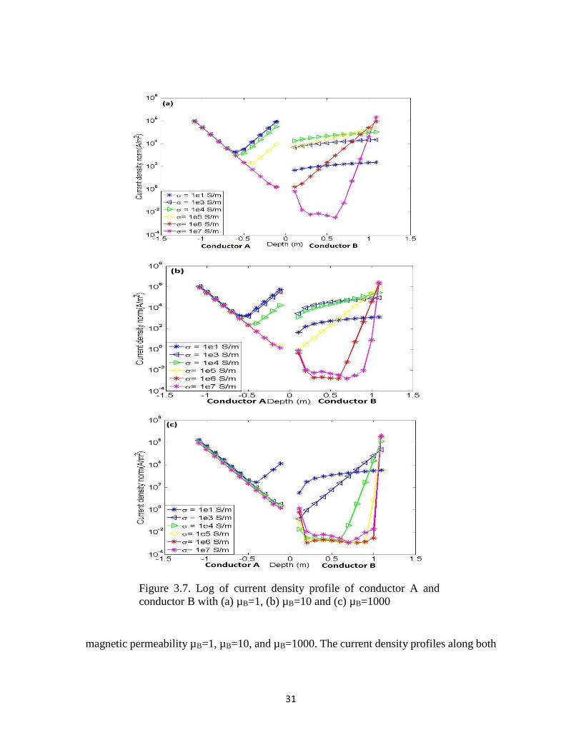
magnetic permeability µB=1, µB=10, and µB=1000. The current density profiles along both
Figure 3.7. Log of current density profile of conductor A and
conductor B with (a) µB=1, (b) µB=10 and (c) µB=1000
32
conductor’s width direction are shown in Fig. 3.7. Our observations are as follows:
1. From Fig. 3.7 (a), we can observe that when the conductivity of conductor B is
very low ( σB=1e1 or 1e2 ), the proximity effect is not significant, therefore the
current density distribution along conductor A is similar to that of the single
conductor case. When σB=1e6, conductor A and conductor B have identical
material properties, the current density profile of conductor A and conductor B are
symmetric.
2. The current density distribution of the outer surface of conductor A is not affected
by conductivity variation of conductor B when the permeability of conductor B is
identical with the permeability of conductor A. The gradient of current density
profile remains unchanged. However, when the permeability of conductor B
increases, the magnitude of current density on the outer surface of conductor A
slightly decreases with the increasing of the conductivity of conductor B.
3. When the permeability of
conductor B is fixed, the saddle
point of current density profile of
conductor A is greatly
determined by the conductivity
variation of conductor B. We
also plot the current density
profile variation with
conductivity σB=1e4 S/m and
Figure 3.8. Log of current density profile
of conductor A and B when σB=1e4 S/m
and µB=1, 10, 1000.
33
permeability µB=1, 10, 1000, as shown in Fig. 3.8. The saddle point is greatly
related with the permeability of conductor B as well. With the increasing of µB, the
proximity effect on the current distribution on conductor A increases.
4. Furthermore, Fig 3.7 (a-c) show that when µAσA =µBσB, the current density profile
of two conductors remain symmetric. In fact, the current density distribution in A
is a function of the product of (μB.σB) of conductor B at a given frequency. This
means that the gradient of current density in conductor A remains unchanged, while
we modify the magnitude of σB and µB by keeping σBµB as a constant.
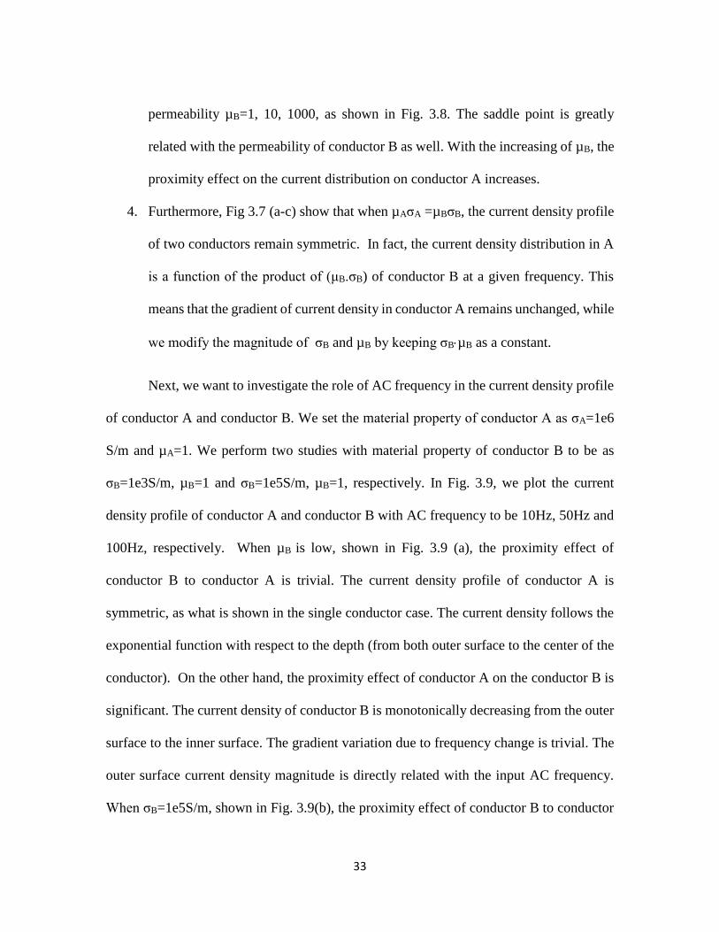
Next, we want to investigate the role of AC frequency in the current density profile
of conductor A and conductor B. We set the material property of conductor A as σA=1e6
S/m and µA=1. We perform two studies with material property of conductor B to be as
σB=1e3S/m, µB=1 and σB=1e5S/m, µB=1, respectively. In Fig. 3.9, we plot the current
density profile of conductor A and conductor B with AC frequency to be 10Hz, 50Hz and
100Hz, respectively. When µB is low, shown in Fig. 3.9 (a), the proximity effect of
conductor B to conductor A is trivial. The current density profile of conductor A is
symmetric, as what is shown in the single conductor case. The current density follows the
exponential function with respect to the depth (from both outer surface to the center of the
conductor). On the other hand, the proximity effect of conductor A on the conductor B is
significant. The current density of conductor B is monotonically decreasing from the outer
surface to the inner surface. The gradient variation due to frequency change is trivial. The
outer surface current density magnitude is directly related with the input AC frequency.
When σB=1e5S/m, shown in Fig. 3.9(b), the proximity effect of conductor B to conductor
34
A becomes more significant, causing the saddle point of current density profile in
conductor A to shift to the inner surface. At the same time, the gradient variation of current
density in conductor B due to the frequency becomes significant.
Figure 3.9 Effect of frequency on current distribution in (a) Conductor B:
μ=1, σ=1e3S/m & (b) Conductor B: μ=1, σ=1e5S/m.
35
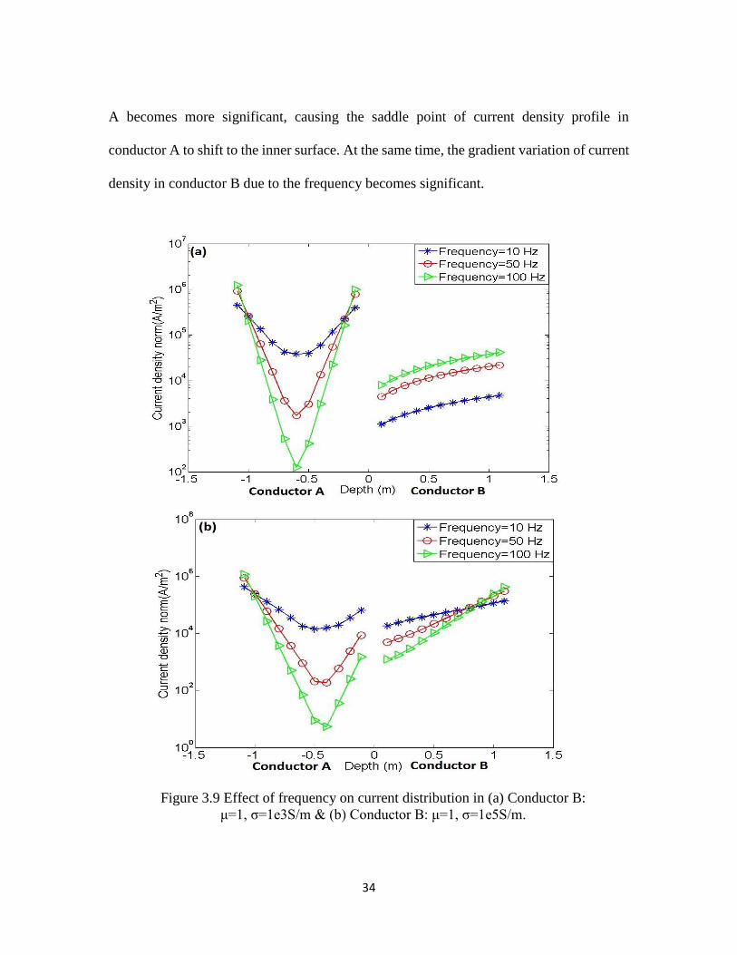
Table 3.1 Material parameter matrix for conductor B
SET Conductivity σB (S/m) Permeability(μB) Frequency f(Hz)
B 1e5 1 100
C 1e4 100 10
D 4e3 100 25
E 1e4 1 1000
REFERENCE 1e6 1 10
The last study is about the combination effect of AC frequency, electrical
conductivity and magnetic permeability to the current density profile. With the two
conductor model, we set σA=1e6 S/m and µA=1 for conductor A. The material parameter
matrix is shown in Table 3.1. With 5 different material setup, we keep the product of
µBσBf to be the same. In Fig 3.10, the reference current density profile is when conductor
A and conductor B are identical. From Fig 3.10. Since the product of µBσBf remains the
same for these 5 cases, both the shape and the magnitude of current density profile for
conductor B are identical. On the other hand, the shape of current density profile in
conductor A is only
depending on the product
of µBσB, as we see that the
current density profile in
conductor A with set B and
set reference are different,
even though the product of
f, µB, σB are identical. Figure 3.10. Effect of frequency on current
distribution in the substrate.
36
3.5 Conclusion
In this chapter, we adopt the two parallel conductors model to investigate the skin
effect, proximity effect and their relation with the conductivity, permeability of the
conductors and the input AC frequency. Our conclusion is as follows:
1. We verified our FEA model results by comparing them with the analytical
results of single conductor skin effect and two parallel identical conductor anti-
proximity effects.
2. We investigate the proximity effect of two parrallel conductors with different
conductivities and permeabilities. Under the condition of µBσB µAσA, the
current density profile of conductor B decreases monotonically from the outer
surface to the inner surface. The slope of the current density is a function of µB,
σB, and f, but remain unchanged when µBσBf is a constant. On the other hand,
the shape of current density profile of conductor A is determined by µB, and σB,
regardless of the frequency f. The frequency f only affect the slope of current
density profile of conductor A. With same AC frequency when µBσB is a
constant, the shape of the current remains the same.
37
CHAPTER 4. CO-PLANAR ELECTRODE MODEL
In this chapter, we investigate a co-planar electrode model which includes a thin
coating, a substrate and three electrodes. With the input AC applied on one electrode, the
current density profile within the coating and substrate is developed. In this chapter, we
first explain the model setup, then we investigate the effect of the coating material property
on the current density profile. By the end, we reach a conclusion.
4.1 Model Setup and Meshing Analysis
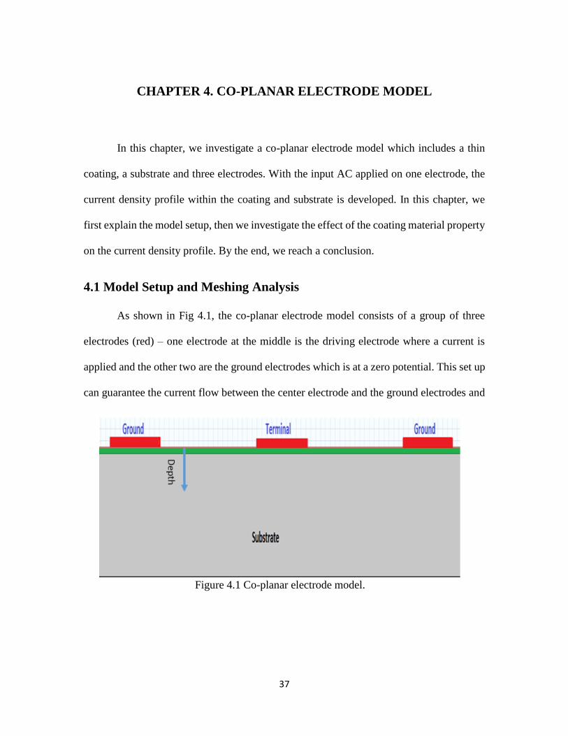
As shown in Fig 4.1, the co-planar electrode model consists of a group of three
electrodes (red) – one electrode at the middle is the driving electrode where a current is
applied and the other two are the ground electrodes which is at a zero potential. This set up
can guarantee the current flow between the center electrode and the ground electrodes and
Figure 4.1 Co-planar electrode model.
38
reducing the current traveling along the other boundaries of the simulation domain. The
thin layer (green) with a thickness of 50mm is the proposed multi-functional ceramic
coating whose conductivity and permeability can be controlled. The bulk domain (gray)
with a depth of 1000mm beneath the coating is the metallic substrate. The ratio of the
electrode size to spacing is 0.5.
The detail finite element model setup through COMSOL is as follows:
1. Substrate : Structural steel
Width=10m
Height=1m
Thickness=1m
Electrical conductivity : 1e6
Relative magnetic permeability: 1
2. Multi-functional ceramic coating: Ceramic mullite
Width=1m
Height=50mm
Thickness=1m
Electrical conductivity: variable (0, 1e6]
Relative magnetic permeability : variable [1, )
3. Current at center electrode: 1e5 Amperes
4. Ground at side electrodes: 0 volts
5. Frequency of current : variable (based on the mesh convergence study)
39
6. Electric insulation (n ∙ J=0) is applied along all boundaries excluding the electrodes
7. Magnetic insulation (𝑛 × 𝐴) is applied along all boundaries
8. The current conservation equation and Ampere’s law are solved across the entire
domain.
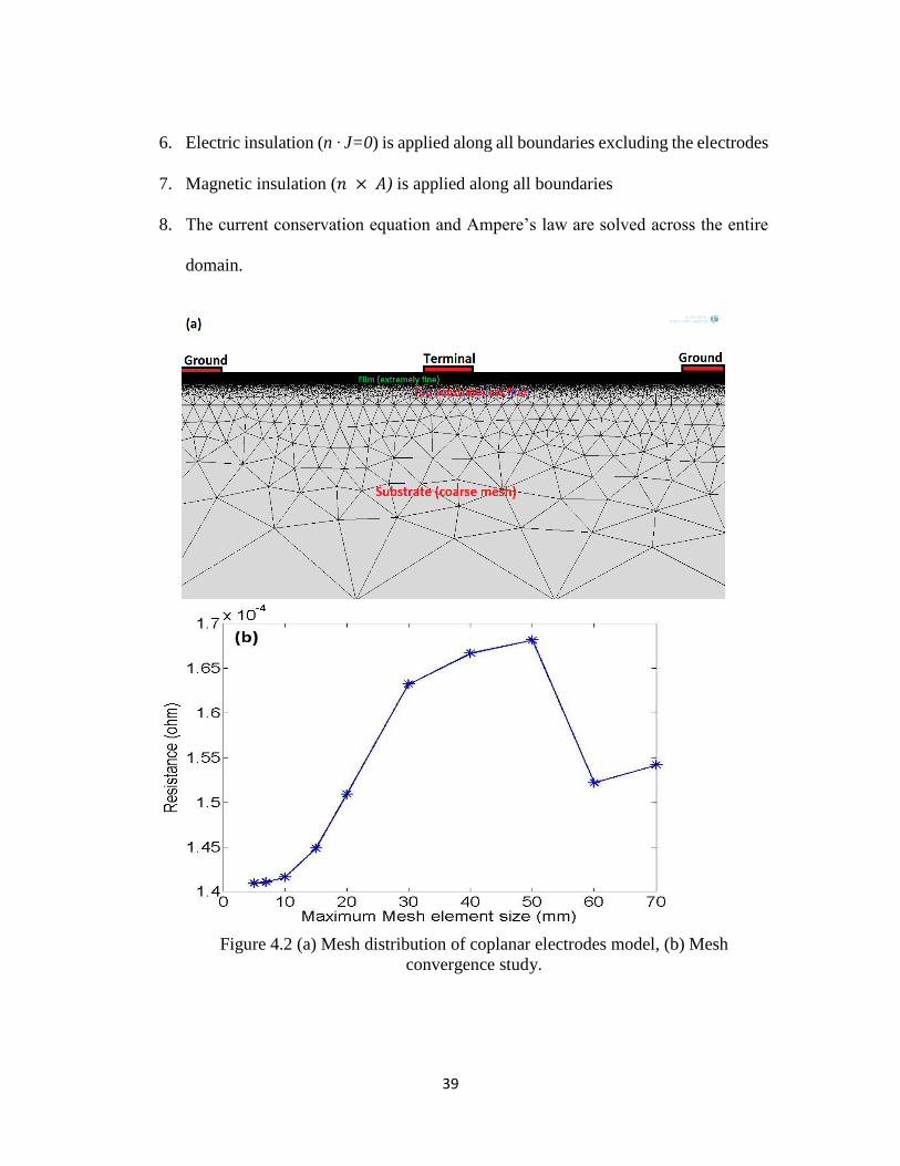
Figure 4.2 (a) Mesh distribution of coplanar electrodes model, (b) Mesh
convergence study.
40
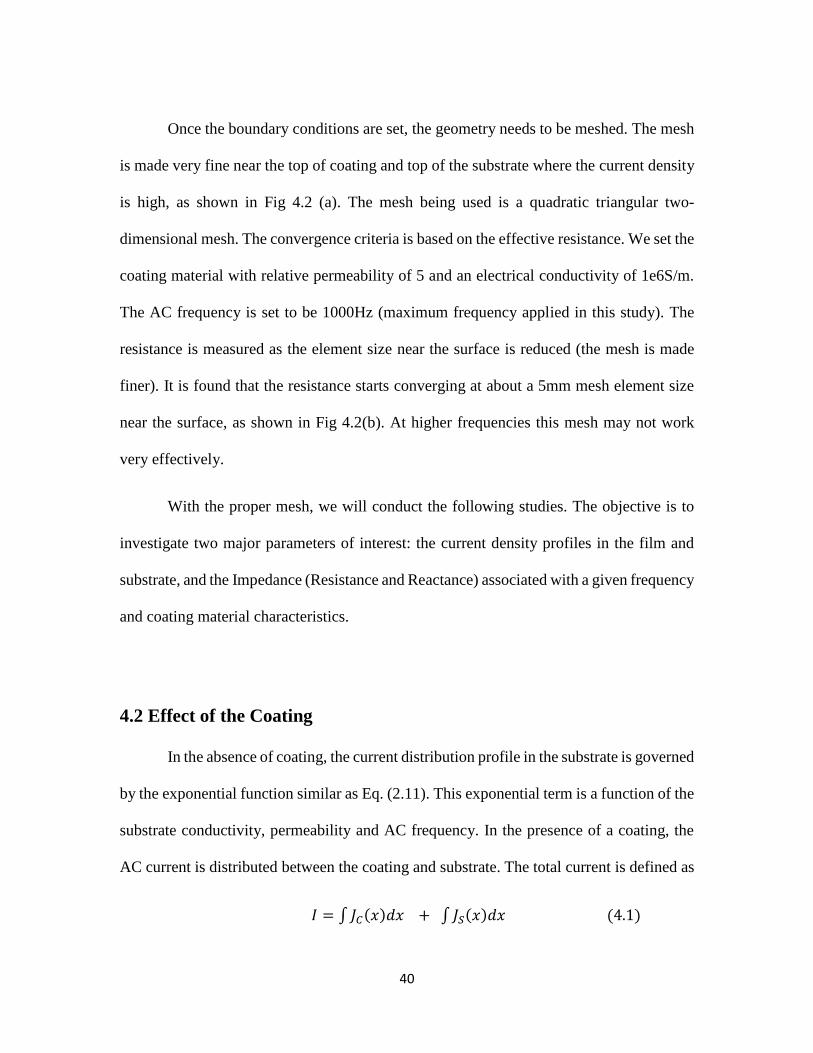
Once the boundary conditions are set, the geometry needs to be meshed. The mesh
is made very fine near the top of coating and top of the substrate where the current density
is high, as shown in Fig 4.2 (a). The mesh being used is a quadratic triangular two-
dimensional mesh. The convergence criteria is based on the effective resistance. We set the
coating material with relative permeability of 5 and an electrical conductivity of 1e6S/m.
The AC frequency is set to be 1000Hz (maximum frequency applied in this study). The
resistance is measured as the element size near the surface is reduced (the mesh is made
finer). It is found that the resistance starts converging at about a 5mm mesh element size
near the surface, as shown in Fig 4.2(b). At higher frequencies this mesh may not work
very effectively.
With the proper mesh, we will conduct the following studies. The objective is to
investigate two major parameters of interest: the current density profiles in the film and
substrate, and the Impedance (Resistance and Reactance) associated with a given frequency
and coating material characteristics.
4.2 Effect of the Coating
In the absence of coating, the current distribution profile in the substrate is governed
by the exponential function similar as Eq. (2.11). This exponential term is a function of the
substrate conductivity, permeability and AC frequency. In the presence of a coating, the
AC current is distributed between the coating and substrate. The total current is defined as
𝐼 = ∫ 𝐽𝐶(𝑥)𝑑𝑥 + ∫ 𝐽𝑆(𝑥)𝑑𝑥 (4.1)
41
Where I is the total current, JC (x) and JS(x) are the current density functions for coating
region and substrate region along the depth direction. In other words a part of the current
will flow through the coating and the rest will flow through the substrate.
Let’s consider the coplanar model in Fig 4.1 with/without the coating (by setting the
coating depth to be 0). The substrate has a conductivity of 1e6 S/m and a relative
Permeability of 1. The coating has a conductivity of 1e3 S/m and a relative permeability
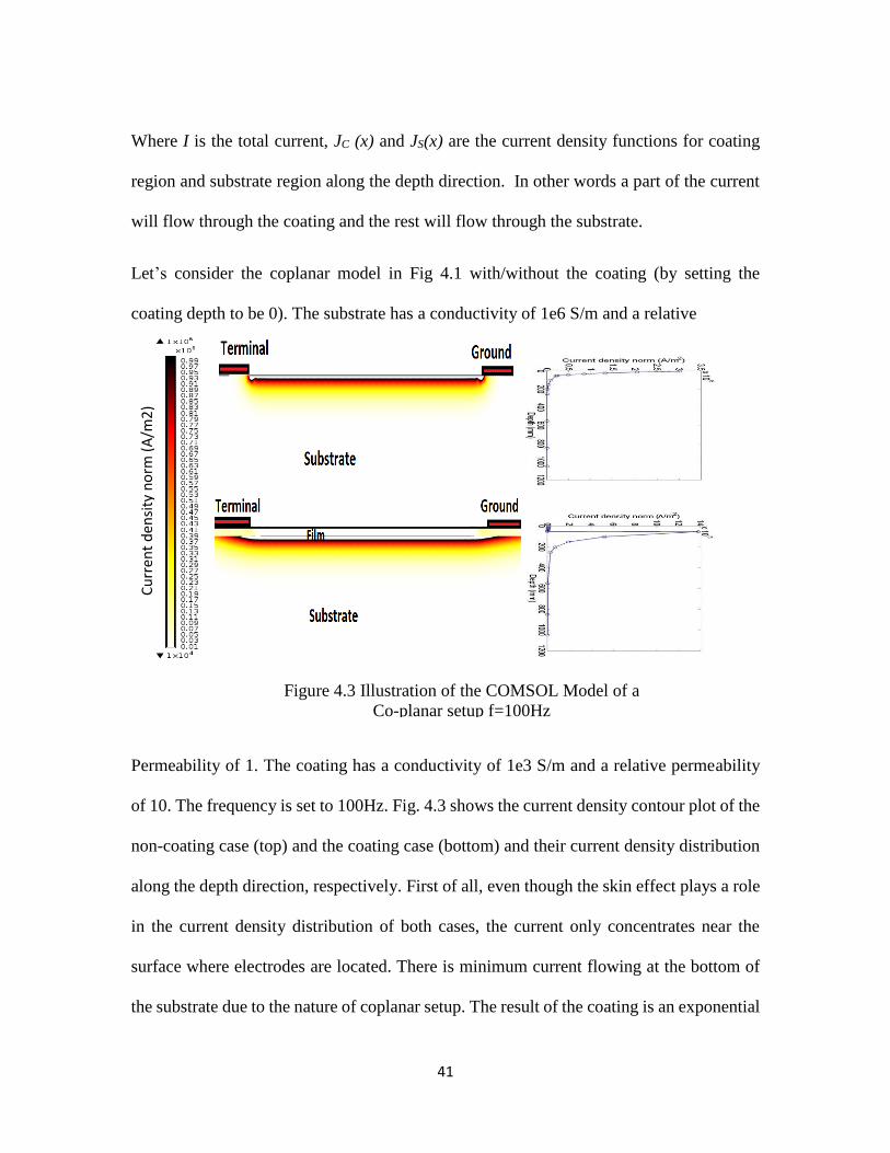
of 10. The frequency is set to 100Hz. Fig. 4.3 shows the current density contour plot of the
non-coating case (top) and the coating case (bottom) and their current density distribution
along the depth direction, respectively. First of all, even though the skin effect plays a role
in the current density distribution of both cases, the current only concentrates near the
surface where electrodes are located. There is minimum current flowing at the bottom of
the substrate due to the nature of coplanar setup. The result of the coating is an exponential
Cu
rren
t d
ensi
ty n
orm
(A
/m2
)
Figure 4.3 Illustration of the COMSOL Model of a
Co-planar setup f=100Hz
42
current distribution in the coating followed by an exponential current distribution in the
substrate. In the non-coating case, the current density profile within the substrate follows
the form of an exponential function. In the coating case, the current density profile within
the coating region and substrate region are both following the form of an exponential
function. There is a current density discontinuity at the coating-substrate interface, due to
the proximity effect.
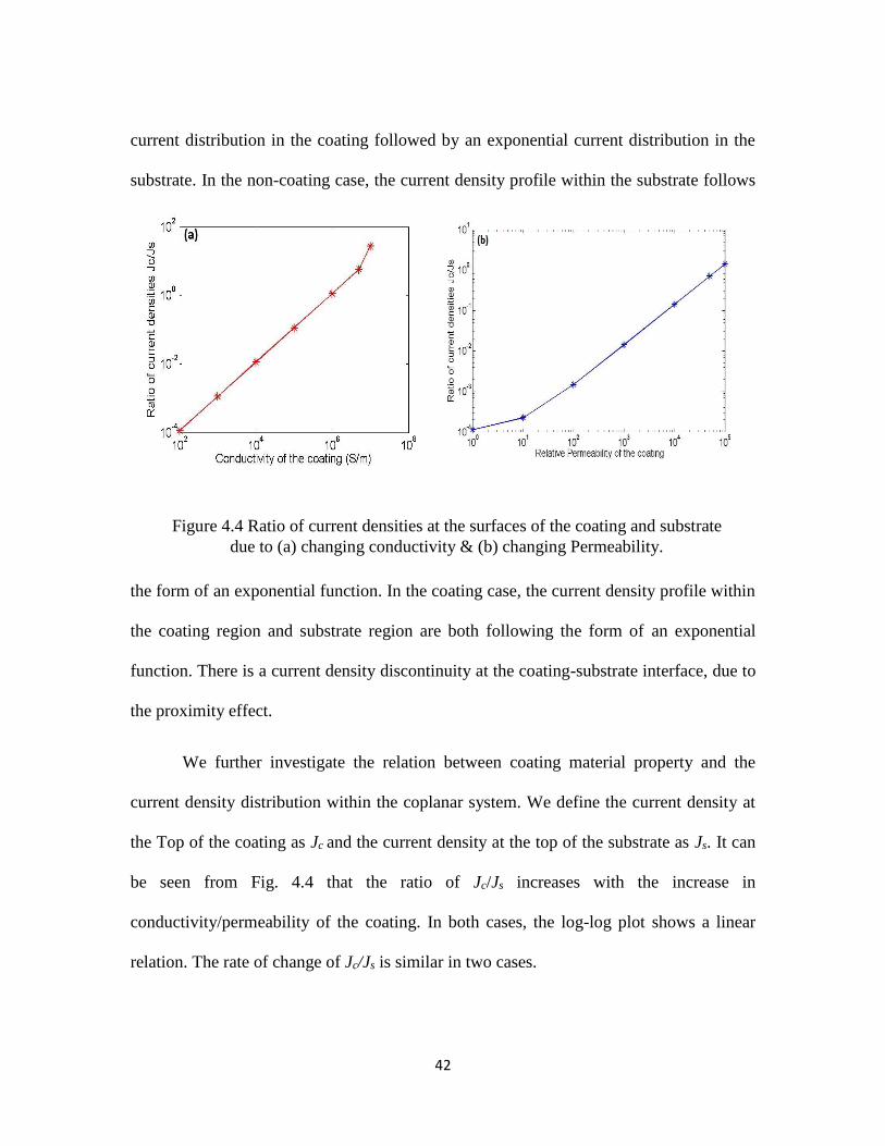
We further investigate the relation between coating material property and the
current density distribution within the coplanar system. We define the current density at
the Top of the coating as Jc and the current density at the top of the substrate as Js. It can
be seen from Fig. 4.4 that the ratio of Jc/Js increases with the increase in
conductivity/permeability of the coating. In both cases, the log-log plot shows a linear
relation. The rate of change of Jc/Js is similar in two cases.
Figure 4.4 Ratio of current densities at the surfaces of the coating and substrate
due to (a) changing conductivity & (b) changing Permeability.
43
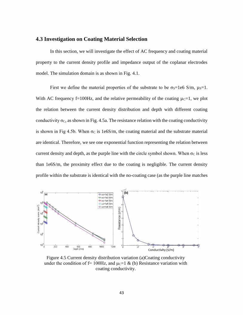
4.3 Investigation on Coating Material Selection
In this section, we will investigate the effect of AC frequency and coating material
property to the current density profile and impedance output of the coplanar electrodes
model. The simulation domain is as shown in Fig. 4.1.
First we define the material properties of the substrate to be σS=1e6 S/m, µS=1.
With AC frequency f=100Hz, and the relative permeability of the coating µC=1, we plot
the relation between the current density distribution and depth with different coating
conductivity σC, as shown in Fig. 4.5a. The resistance relation with the coating conductivity
is shown in Fig 4.5b. When σC is 1e6S/m, the coating material and the substrate material
are identical. Therefore, we see one exponential function representing the relation between
current density and depth, as the purple line with the circle symbol shown. When σC is less
than 1e6S/m, the proximity effect due to the coating is negligible. The current density
profile within the substrate is identical with the no-coating case (as the purple line matches
Figure 4.5 Current density distribution variation (a)Coating conductivity
under the condition of f= 100Hz, and μC=1 & (b) Resistance variation with
coating conductivity.
44
well with the other lines after a translational shift along the depth direction). The decrease
in resistance is greatly related with the increase of coating conductivity. The surface current
density JC is monotonically increasing with an increase of coating conductivity.
Next, we investigate the relation between coating permeability/AC frequency and
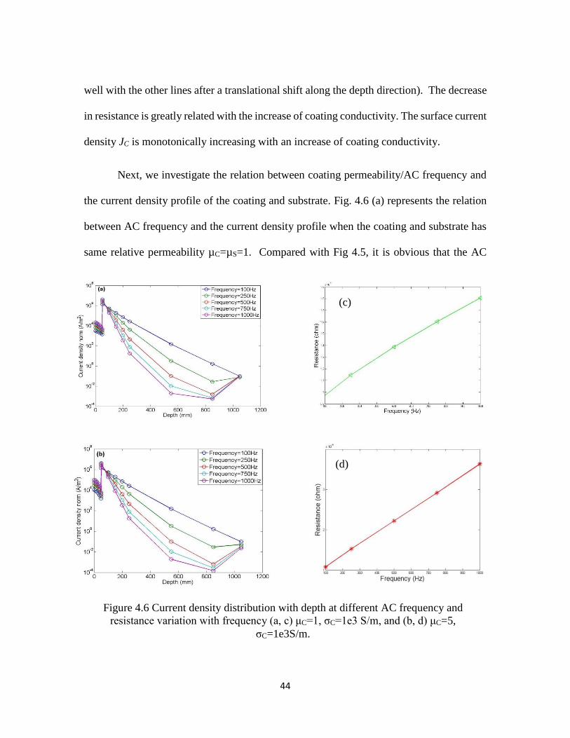
the current density profile of the coating and substrate. Fig. 4.6 (a) represents the relation
between AC frequency and the current density profile when the coating and substrate has
same relative permeability µC=µS=1. Compared with Fig 4.5, it is obvious that the AC
Figure 4.6 Current density distribution with depth at different AC frequency and
resistance variation with frequency (a, c) μC=1, σC=1e3 S/m, and (b, d) μC=5,
σC=1e3S/m.
(c)
(d)
45
frequency affects the current density profile in the substrate significantly. The frequency
effect to the current density profile in the coating region is not as significant as coating
conductivity effect. Fig 4.6 (b) represents the current density profile variation with respect
to the frequency when the permeability of coating is 5 times of the permeability of the
substrate. It is obvious that permeability effect is trivial compared with the frequency
effect. With the increased coating permeability, the current distribution in the coating
region is more sensitive to the frequency changes. In both cases, the resistance depicts a
Figure 4.7 Surface and Interface current densities variation
with coating conductivity for (a) μC=1, and (b) μC=5.
46
Linearly increasing trend with respect to the frequency increase. It is greatly related with
the current density distribution within the substrate.
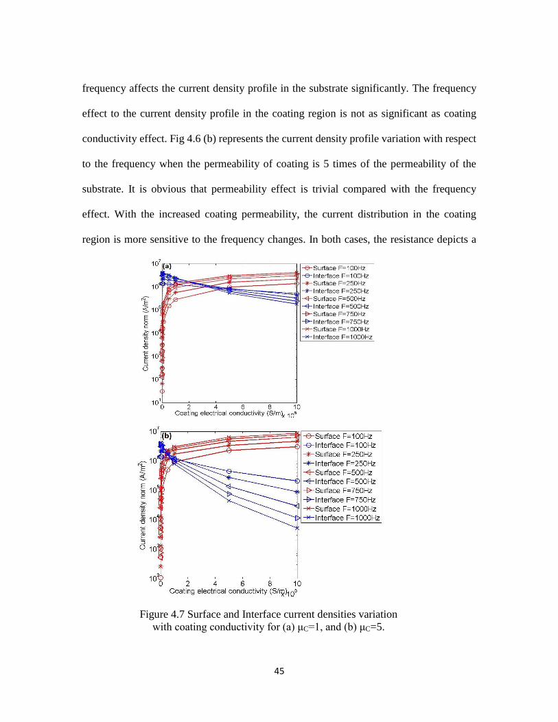
We also plot the magnitude variation of current density at the coating surface and
coating-substrate interface with coating conductivity, coating permeability and input AC
frequency, as shown in Fig. 4.7. It is clear that with the increased coating permeability, the
coating conductivity variation effect to the interface current density becomes significant.
With the increasing of frequency, the coating surface current density increases and the
interface current density decreases, which is due to the skin effect. On the other hand, with
higher coating permeability, the magnitude of coating surface current density increases
dramatically.
4.4 Simulation Limitation: Boundary Coupling Effect
When the model was set up such that the coating was about 5 microns and substrate
was about 2mm (2000microns) it was found that the current density at the bottom of the
coating was significantly high when the operating frequency range was 100-1000Hz. This
is because the skin depth was significantly large when compared to the substrate depth.
This resulted in large current density values at the bottom of the substrate where an electric
insulation boundary condition was applied. In other words at the boundary,
𝑛 . 𝐽 = 0 (4.2)
47
Where n is the outward normal and J is the current density. As a result for such
small scale dimensions the operating frequency has to be significantly large so that at the
bottom of the substrate the current density is negligibly small. This prevents any coupling
between current density at that point and the electric insulation boundary condition. At
larger frequencies the skin depth is significantly smaller than the substrate itself which is
necessary for modelling the correct physics.
Typically due to skin effect, current tends to flow at the boundaries. In the co planar
setup with a single terminal and ground, current would flow along the bottom of the
substrate in addition to between the electrodes. In order to minimize the current flow at the
bottom of the substrate we introduce the three electrode setup. This reduces the net current
flowing towards the bottom, which would not be expected experimentally when the
substrate is large.
4.5 Conclusion
Through the co-planar electrode study, we reach to the following conclusion:
1. When µCσC µSσS, the current density profile of the substrate is not affected by the
coating conductivity, but affected by the AC frequency.
2. The effective resistance is greatly related with the coating conductivity and AC
frequency.

48
Therefore, we expect the multifunctional ceramics coating will not greatly improve the
ACPD signal sensitivity for the interface crack, which will be discussed in the next chapter.
49
CHAPTER 5. CRACK STUDY AND ANALYSIS
In this chapter, we will investigate the signal sensitivity of the coating crack case
and coating-substrate interface crack case, respectively. The crack is modelled as a
triangular notch. The crack is filled with air with electrical conductivity of 0 S/m and
relative permeability of 1. The presence of the crack causes the current to maneuver around
increasing the effective resistance. Thus, the absolute/relative resistance variation can be
evaluated with crack size, AC frequency and coating material properties. Finally,
conclusions will be drawn in the end.
5.1 Model and Mesh Analysis
We adopt the model in Fig 4.1 by adding a triangular shaped crack either on the top
of the surface or at the interface of the surface. The detail mesh for the surface crack is
shown in Fig 5.1. The crack region is modeled with the conductivity and permeability of
air. In the coating region, we apply the extremely fine mesh in order to keep the accuracy
of current density. At the top of the substrate the mesh is made less fine and is extremely
coarse into the substrate.
Figure 5.1 Mesh around the crack.
50
5.2 Coating Crack Analysis
This section is divided into two parts. In the first part we will study the current
density profile due to the presence of a coating crack and the change in current flow. In the
second part we will analyze the change in resistance due to the presence of the crack in the
coating when compared to a case which has no coating.
The simulation domain is similar with Fig 4.1. In this case, the coating was taken
to be 50mm thick and substrate is 1000mm. The ratio of the electrode size to the electrode
spacing is set as 0.5. The crack has a base of 100mm and height of 50mm inside the coating.
The substrate conductivity σS is 1e6 S/m and the permeability µS is 1. The frequency is
varied from 100-1000Hz. The current density profiles are plotted for two different
permeability’s of 1 and 5, each of which has conductivities varying from 1e2-1e6 S/m over
the frequency range. Fig. 5.2 shows the current density profile of this simulation domain
Figure 5.2 COMSOL model representing current flow around a coating crack at 1000Hz
51
under the condition of σC=1e6 S/m, µC=1 and the AC frequency is f=1000Hz. We can
clearly see the crack causes the current density concentration at the crack tip within the
substrate.
5.2.1 Current Density Profiles for a Coating Crack
Two specific cases have been chosen to represent the current density profiles along
the depth direction at the crack tip as shown in Fig 5.3 and Fig 5.4. Fig. 5.3 represents the
case for coating relative permeability of µC=1, frequency f= 100Hz and coating
conductivities σC varying from 1e2S/m to 1e6 S/m. Fig. 5.4 represents the case for coating
relative permeability of µC=5, frequency f= 1000Hz and coating conductivities σC varying
from 1e2S/m to 1e6 S/m.
It can be concluded that the current density is zero for points inside the crack.
Similar as our conclusion in Chapter 3 and Chapter 4. The current density profile of the
substrate is mainly depending on the product of coating conductivity and coating
permeability. The input AC frequency plays the dominate role in affecting the gradient of
current density profile within the substrate. At the top of the substrate the current density
increases as the current is pushed downwards from the crack into the substrate as the
conductivity/permeability of the coating increases. The increase in current density at the
bottom of the substrate is due to the skin effect tendency. This effect is more pronounced
at higher frequencies and is significantly reduced by introducing a third electrode as
described previously.
52
Figure 5.3 Current density distribution along the depth direction amd current
density variation with the coating conductivity for a frequency of 100Hz, μC=1.
Figure 5.4 Current density distribution along the depth direction amd current
density variation with the coating conductivity for a frequency of 1000Hz, μC=5.
53
5.2.2 Resistance Calculation for a Coating Crack
The change in resistance for a coating crack is almost negligible due to the
relatively lower operating frequencies of up to 1000Hz. At much higher frequencies where
the change in resistance would be greater the mesh resolution required is high. One case
that was considered was a coating identical to the substrate (conductivity=1e6 S/m and
relative permeability =1). This was compared to a coating coated over the surface
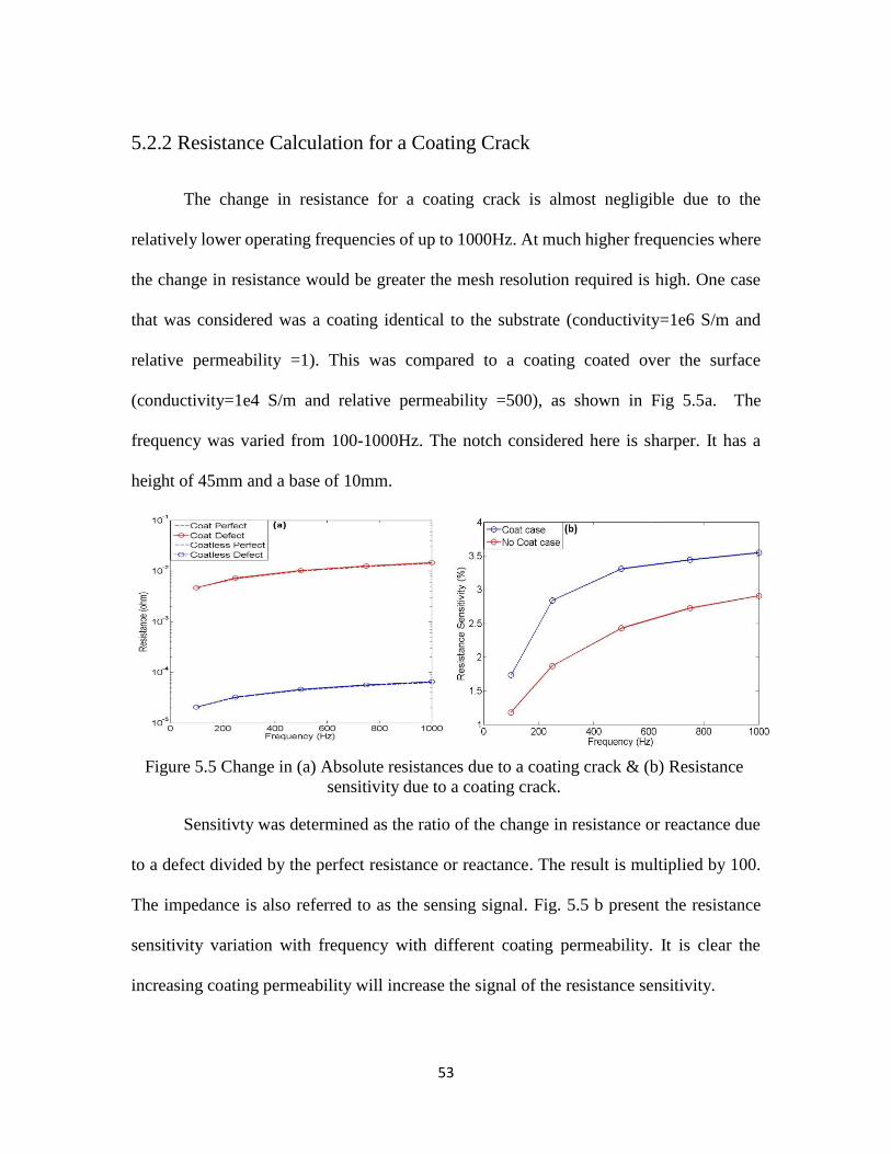
(conductivity=1e4 S/m and relative permeability =500), as shown in Fig 5.5a. The
frequency was varied from 100-1000Hz. The notch considered here is sharper. It has a
height of 45mm and a base of 10mm.
Sensitivty was determined as the ratio of the change in resistance or reactance due
to a defect divided by the perfect resistance or reactance. The result is multiplied by 100.
The impedance is also referred to as the sensing signal. Fig. 5.5 b present the resistance
sensitivity variation with frequency with different coating permeability. It is clear the
increasing coating permeability will increase the signal of the resistance sensitivity.
Figure 5.5 Change in (a) Absolute resistances due to a coating crack & (b) Resistance
sensitivity due to a coating crack.
54
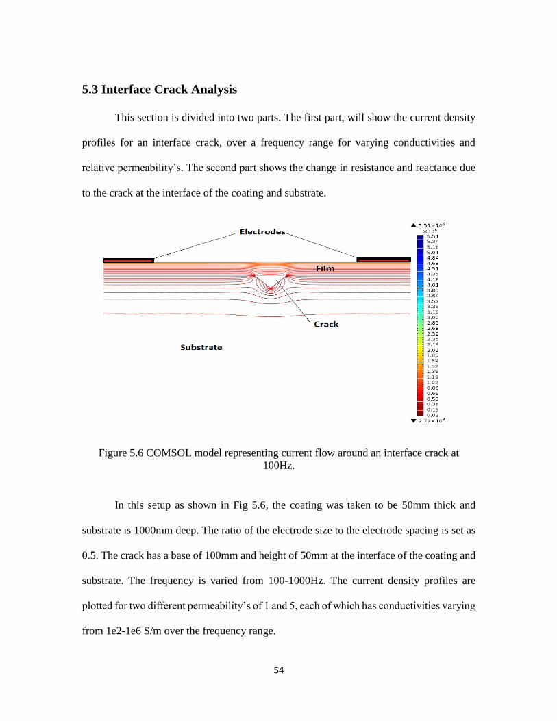
5.3 Interface Crack Analysis
This section is divided into two parts. The first part, will show the current density
profiles for an interface crack, over a frequency range for varying conductivities and
relative permeability’s. The second part shows the change in resistance and reactance due
to the crack at the interface of the coating and substrate.
Figure 5.6 COMSOL model representing current flow around an interface crack at
100Hz.
In this setup as shown in Fig 5.6, the coating was taken to be 50mm thick and
substrate is 1000mm deep. The ratio of the electrode size to the electrode spacing is set as
0.5. The crack has a base of 100mm and height of 50mm at the interface of the coating and
substrate. The frequency is varied from 100-1000Hz. The current density profiles are
plotted for two different permeability’s of 1 and 5, each of which has conductivities varying
from 1e2-1e6 S/m over the frequency range.
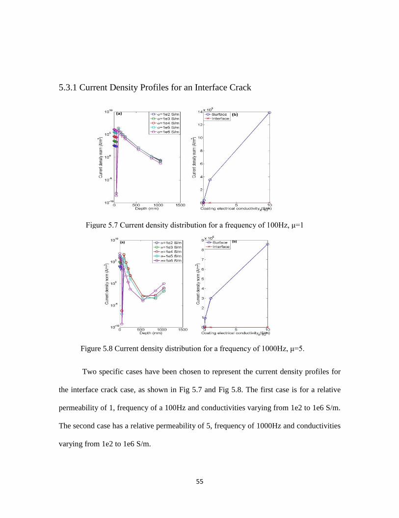
55
5.3.1 Current Density Profiles for an Interface Crack
Two specific cases have been chosen to represent the current density profiles for
the interface crack case, as shown in Fig 5.7 and Fig 5.8. The first case is for a relative
permeability of 1, frequency of a 100Hz and conductivities varying from 1e2 to 1e6 S/m.
The second case has a relative permeability of 5, frequency of 1000Hz and conductivities
varying from 1e2 to 1e6 S/m.
Figure 5.8 Current density distribution for a frequency of 1000Hz, μ=5.
Figure 5.7 Current density distribution for a frequency of 100Hz, μ=1
56
The current density profile of the substrate is mainly depending on the product of
coating conductivity and coating permeability. The input AC frequency plays the dominate
role in affecting the gradient of current density profile within the substrate. At the top of
the substrate the current density increases as the current is pushed downwards from the
crack into the substrate as the conductivity/permeability of the coating increases. The
increase in current density at the bottom of the substrate is due to the skin effect tendency.
This effect is more pronounced at higher frequencies and is significantly reduced by
introducing a third electrode as described previously.
5.3.2 Impedance Calculations for an Interface Crack
The change in resistance and reactance for an interfacial crack was carried out for
a model on a micron dimension scale, which relaxed the meshing requirements, shown in
Fig 5.9. As a result the frequency used was significantly high of the order of 1 MHz. The
coating was 5 microns in thickness and the substrate was 2mm deep. The crack geometry
has a depth of 200 microns and a base of 200 microns too. The change in resistance was
more significant because more current was found to maneuver around the crack at this
reduced skin depth. The frequency was fixed at 1 MHz and two cases of relative
permeability of 1 and 100 were studied. Each case has its electrical conductivity varying
from 1e2-1e4 S/m.
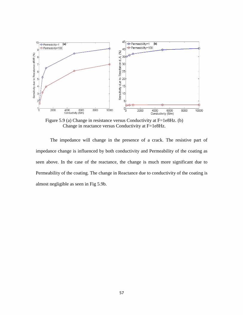
57
The impedance will change in the presence of a crack. The resistive part of
impedance change is influenced by both conductivity and Permeability of the coating as
seen above. In the case of the reactance, the change is much more significant due to
Permeability of the coating. The change in Reactance due to conductivity of the coating is
almost negligible as seen in Fig 5.9b.
Figure 5.9 (a) Change in resistance versus Conductivity at F=1e8Hz. (b)
Change in reactance versus Conductivity at F=1e8Hz.
58
CHAPTER 6. CONCLUSIONS AND FUTURE WORK
6.1 Accomplishments:
1. Understood the advantage of ACPD (Alternating current potential drop) over
DCPD (Direct current potential drop) which helps determine the location of a crack
based on frequency resolution.
2. Understood the concepts of skin effect and proximity effect in detail, the associated
equations, and parameters associated with them.
3. Setup a simple two conductor parallel model in COMSOL Multiphysics with the
correct toolbox and boundary conditions. The results of these simulations were also
validated using analytical models.
4. Determined that the setup was similar to a parallel RL circuit where the current
branches and only the sum of the current in the film and substrate are constant.
5. Carried out a crack analysis for a film crack and an interface crack and studied the
current density profiles for each.
6. Carried out an impedance study for the interface crack case and drew some
conclusions.
59
6.2 Conclusions:
1. Determined similarities in the behavior of the current density profile based on the
product relationship (μσ) in the substrate for the parallel conductor case.
2. Analyzed the current density profiles for a Co-planar model setup for varying
frequency, relative permeability and electrical conductivity.
3. The strength of the surface current density in the substrate drops for an increase in
conductivity of the film due to the proximity effect.
4. The physics of the current density profile in the substrate will not change when a
film is coated over the surface of the substrate simply because the exponential
functional term for current distribution remains unaffected and only surface current
density changes. This will result in a set of parallel lines on a semi-log plot.
5. The change in impedance in the film is almost negligible when a defect is present
because the defect is very small. The skin depth needed to see a significant change
here would have to be smaller than the defect which is a computational limitation.
6. The change in resistance due to a crack is a function of the crack size (area) to the
unaffected area, as well as the crack geometry.
7. The change in reactance for a change in conductivity of the film is negligible. The
significant difference here is due to permeability of the film.

60
6.3 Scope for Future Work:
1. To understand the concept of tunneling current at the percolation threshold more
strongly and computationally model it.
2. The benefit of conducting current through a ceramic while maintaining other
physical and mechanical properties.
3. Studying the effect of strain due to loading on the effective resistance of the matrix
and to try to establish a relationship between the two.
4. To help improve the sensing signal (like change in impedance) after locating the
crack in the model.
61
REFERENCES
[1] NDT Resource center, https://www.nde-ed.org/AboutNDT/aboutndt.htm.
[2] The American society for non-destructive testing, https://www.asnt.org/.
[3] Javier Garcia-Martín, Jaime Gómez-Gil, and Ernesto Vazquez-Sánchez, 2011
“Non- Destructive Techniques Based on Eddy Current Testing”, Sensors, Volume 11,
Issue 3, 2525-2565.
[4] http://www.isnt.org/ndt_methods.pdf
[5] http://www.engineeringtoolbox.com/ndt-non-destructive-testing-d_314.html
[6] Mark Willcox and George Downes, 2000, “A Brief Description of NDT Techniques”,
Insight NDT Equipment Limited.
[7] L. Santandrea, Y. Le. Bihan, 2010, “Using COMSOL Multiphysics in eddy current
non-destructive testing context”, Excerpt from the Proceedings of the COMSOL
Conference Paris.
[8] Tribikram Kundu, 2012, “Ultrasonic and Electromagnetic NDE for Structure and
Material Characterization”, Engineering and Biomedical Applications, CRC Press, Taylor
and Francis Group.
[9] H. Saguy and D. Rittel, 2005, “Bridging thin and thick skin solutions for alternating
currents in cracked conductors”, applied physics letters 87.
[10] “The practical aspects of the ACPD technique”, User Manual, Matelect
62
[11] H. Saguy and D. Rittel, April 2007, “Flaw detection in metals by the ACPD technique:
Theory and experiments”, NDT&E International, Elsevier.
[12] W.D. Dover and C.C. Monahan, 2007, “The Measurement of Surface Breaking Cracks
by the Electrical Systems ACPD/ACFM”, Fatigue and Fracture of Engineering Materials
and Structures, Volume 17, Issue 12, pages 1485–1492.
[13] Ning Hu,Yoshifumi Karube, Cheng Yan, Zen Masuda, Hisao Fukunaga, 2008
“Tunneling effect in a polymer/ carbon nanotube nanocomposite strain sensor”, Acta
Materialia 56, 2929-2936.
[14] D.Toker, D Azolay, N. Shimaoni, I. Balberg, O. Millo, July 2003, “Tunneling and
percolation in metal insulator composite materials”, Physics. Rev. B68, 041403(R).
[15] http://en.wikipedia.org/wiki/Percolation_threshold
[16] http://en.wikipedia.org/wiki/Quantum_tunnelling
[17] S.O. Kasap, 2006, “Principles of electronic materials and devices”, 3rd edition,
published by McGraw Hill.
[18] D. Musuwathi Ekanath, N. Badi, A. Bensaoula, 2011, “Modelling and simulation of
artificial core-shell based nano-dielectrics for electrostatic capacitors applications”,
Excerpt from the proceedings of the COMSOL conference in Boston.
[19] Ceramic coatings for metal parts,
http://www.thomasnet.com/articles/chemicals/ceramic-coating-metals.
63
[20] http://www.competitiveedgecoatings.com/pages/ceramic_coating.php
[21] https://www.startinglineproducts.com/technical.cfm?articleID=18
[22] http://www.cdxetextbook.com/fuelSys/intakeExhaust/exComp/ceramiccoatings.html
[23] http://en.wikipedia.org/wiki/Electrical_impedance
[24] Marian K. Kazimeirczuk, 2014, “High Frequency Magnetic components”, Second
edition, published by John Wiley & Sons.
[25] http://en.wikipedia.org/wiki/Lenz%27s_law
[26] H. Saguy and D. Rittel, 2007,”Application of AC tomography to crack identification”,
applied physics letters 91.
[27] Andrei Szilagyi , Feb 2014, “Chapter 20 - The skin effect”.
[28] Douglas Brooks, 2010, “Skin effect”, 2010 Ultracad Design, Inc.
[29] Robert W Ericson, Dragan Maksimovic, “Fundamentals of Power electronics”,
University of Colorado Boulder, Second edition.
[30] Marian Greconici, Gheorghe Madescu, and Martian Mot, September 2009, “Skin
effect analysis in a free space conductor”, 9th international conference on applied
electromagnetics, Serbia.
64
[31] Xi Nan and Charles R. Sullivan, June 2003, “An improved calculation of proximity
– effect loss in high frequency windings of round conductors”, Power electronics specialist
conference, 853-860, Vol 2.
[32] “AC/DC Module user’s guide”, May 2012, COMSOL 4.3.
Related Documents


