Comparison of Elastic Modulus of Very Thin DLC Films Deposited by r.f.-PACVD and FVA Jin-Won Chung, Churl-Seung Lee, Dae Hong Ko * , Jun-Hee Hahn ** and Kwang-Ryeol Lee Future Technology Research Division, Korea Institute of Science and Technology * Department of Ceramics, Yonsei University ** Korea Research Institute of Standard Science

Comparison of Elastic Modulus of Very Thin DLC Films Deposited by r.f.-PACVD and FVA
Jan 01, 2016
Comparison of Elastic Modulus of Very Thin DLC Films Deposited by r.f.-PACVD and FVA. Jin-Won Chung, Churl-Seung Lee, Dae Hong Ko * , Jun-Hee Hahn ** and Kwang-Ryeol Lee Future Technology Research Division, Korea Institute of Science and Technology - PowerPoint PPT Presentation
Welcome message from author
This document is posted to help you gain knowledge. Please leave a comment to let me know what you think about it! Share it to your friends and learn new things together.
Transcript
Comparison of Elastic Modulus of Very Thin DLC Films Deposited by
r.f.-PACVD and FVA
Jin-Won Chung, Churl-Seung Lee, Dae Hong Ko*,
Jun-Hee Hahn** and Kwang-Ryeol Lee
Future Technology Research Division, Korea Institute of Science and Technology
* Department of Ceramics, Yonsei University
** Korea Research Institute of Standard Science

Applications of DLC Film

High Residual Compressive Stress of DLC Films
• Causes the Instability of the Coating• Affects the Physical Properties in Some Cases
DLC Coating

Self Delamination of DLC Films
• K.-R. Lee et al., Diam. Rel. Mater. 2 (1993) 208.• M.-W. Moon et al., Acta Mater., 50 (2002) 1219.

Key Idea of the Method
1
E
For Isotropic Thin Films

Measurement of Residual Stress
• Assumption– 1-D Treatment of Elastic
Equilibrium
– Sufficient Adhesion
– df << ds
– ds << R
sff
ssf
ss
ff
f
ssf
ddd
dY
R
dE
dE
d
dY
R
for 6
1
16
1
2
2
sff
ssf
ss
ff
f
ssf
ddd
dY
R
dE
dE
d
dY
R
for 6
1
16
1
2
2
R
ds
df
ss
ff
f
bf
sfbf
dY
dY
R
dY
3
2
ss
ff
f
bf
sfbf
dY
dY
R
dY
3
2

Measurement of Curvature
dx
dK
sin
dx
dK
sin

Key Idea of the Method
For Isotropic Thin Films
1
E

Preparation of DLC Bridge by Micro Fabrication
DLC film Deposition ( on SiO2 )
DLC PatterningSiO2 Isotropic Wet Etching
Wet Cleaning
Strain Estimation

Microstructure of DLC Bridges
C6H6, 10mTorr, -400V, 0.5m
150m

Strain of the Buckled Thin Films (I)
xco
E
)1(
t
D
xAxW
x
Wt
x
WD
c
o
c
x
WWx
x
WWx
2
2
2
2
4
4
4
2cos1)(
0
0 ,2
at
0 ,2
at
z
x
2A0
c
c

Stain of the Buckled Thin Films (II)
2
2
2
2
2 2
11
2
1
ox
x
x
A
dxx
W
x
W
cooA
E
2
1
0
131
1
13
1
,4
From
2
22
2
2
2
t
A
t
E
t
D
oo
c
c
c
ooA
E
2
1

DLC film Deposition
Cleavage along [011] Direction
Si Etching (by KOH Solution) Wet Cleaning
Strain Measurement
Preparation of Free-overhang by Anisotropic Substrate Etching

Elastic Modulus for Various Ion Energies
0 100 200 300 400 500 600 700 800
0
50
100
150
200
250
Pla
ne
Str
ain
Mod
ulus
(G
Pa
)
Negative Bias Voltage (V)
Nanoindentation t>1.0 ㎛
100 200 300 400 500 600
0
50
100
150
200
Bridge Method
Freehang Method
E/(1
-)
(GPa
)
Negative Bias Voltage (V)

Advantages of This Method
– Simple
– Completely Exclude the Substrate Effect
– Can Be Used for Very Thin Films
The possibility of elastic modulus measurement in very thin film

0 200 400 600 800 1000 1200
25
50
75
100
on Si on W / Si on SiO
2/ Si
Bia
xial
Ela
stic
Mod
ulus
(G
Pa
)
Thickness (nm)
a-C:H, C6H6 -400V
J.-W. Chung et al, Diam.Rel. Mater. 10 (2001) 2069.
ta-C (-50Vb)
Elastic Modulus of Very Thin Films

Synthesis of DLC Film by r.f.-PACVD
• RF PACVD (13.56MHz)
• Precursor : CH4
• Vb/ P1/2 : 20 ~ 233 Vb/mTorr1/2
• Substrate : P type (100) Si
• Film Thickness : ~ 50nm

Residual Stress & G-peak Position of Raman Spectra
0 50 100 150 200 2501520
1525
1530
1535
1540
1545
1550
1555
G-p
ea
k P
osi
tion
(cm
-1)
Vb / P1/2 (V/mTorr1/2)
0 50 100 150 200 250
0.5
1.0
1.5
2.0
2.5
3.0
Res
idua
l Com
pres
sive
Stre
ss (G
Pa)
Vb / P1/2 (V/mTorr1/2)

Biaxial Elastic Modulus
0 100 200 300 400 500 6000
50
100
150
200
Bia
xial
Ela
stic
Mod
ulus
(G
Pa)
Thickness (nm)
0 50 100 150 200 250
0.5
1.0
1.5
2.0
2.5
3.0
Res
idua
l Com
pres
sive
Str
ess
(GP
a)
Vb / P1/2 (V/mTorr1/2)
20

Biaxial Elastic Modulus
0 100 200 300 400 500 6000
50
100
150
200
Bia
xial
Ela
stic
Mod
ulus
(G
Pa)
Thickness (nm)
0 50 100 150 200 250
0.5
1.0
1.5
2.0
2.5
3.0
Res
idua
l Com
pres
sive
Str
ess
(GP
a)
Vb / P1/2 (V/mTorr1/2)
20
100

Biaxial Elastic Modulus
0 100 200 300 400 500 6000
50
100
150
200
Bia
xial
Ela
stic
Mod
ulus
(G
Pa)
Thickness (nm)
0 50 100 150 200 250
0.5
1.0
1.5
2.0
2.5
3.0
Res
idua
l Com
pres
sive
Str
ess
(GP
a)
Vb / P1/2 (V/mTorr1/2)
20
166
100

Biaxial Elastic Modulus
0 50 100 150 200 250
0.5
1.0
1.5
2.0
2.5
3.0
Res
idua
l Com
pres
sive
Str
ess
(GP
a)
Vb / P1/2 (V/mTorr1/2)
0 100 200 300 400 500 6000
50
100
150
200
Bia
xial
Ela
stic
Mod
ulus
(G
Pa)
Thickness (nm)
20
233
166
100

G-peak Position of Raman Spectra
0 300 600 900 12001520
1530
1540
1550
1560
G-p
eak
Pos
ition
(cm
-1)
Thickness (nm)
20
233
166
100
0 100 200 300 400 500 6000
50
100
150
200
Bia
xial
Ela
stic
Mod
ulus
(G
Pa)
Thickness (nm)
20
233
166
100

0 300 600 900 12001520
1530
1540
1550
1560
G-p
eak
Pos
ition
(cm
-1)
Thickness (nm)
233
166
100
20
Schematic Film Structure
Si Substrate
Si Substrate
Si Substrate
0 100 200 300 400 500 6000
50
100
150
200
Bia
xial
Ela
stic
Mod
ulus
(G
Pa)
Thickness (nm)

Synthesis of ta-C Films
• ta-C films on Si (100) Wafer
• Vb : from 0 to –500V

0 100 200 300 400 500 6000
1
2
3
4
5
6
7
Res
idua
l Com
pres
sive
Str
ess
(GP
a)
Negative Bias Voltage (V)
Elastic Modulus of ta-C film
0 100 200 300 400 500100
200
300
400
500
600
700
800
900
35 V 300 V
Bia
xia
l Ela
stic
Mo
du
lus
(GP
a)
Thickness (nm)

0 100 200 300 400 500 6000
1
2
3
4
5
6
7
Res
idua
l Com
pres
sive
Str
ess
(GP
a)
Negative Bias Voltage (V)0 100 200 300 400 500
100
200
300
400
500
600
700
800
900 GND 35 V 300 V
Bia
xia
l Ela
stic
Mo
du
lus
(GP
a)
Thickness (nm)
Elastic Modulus of ta-C film

Raman Spectra
1000 1500 2000 2500
Inte
nsi
ty (
A.U
.)
Raman Shift (cm -1)
16 nm 86 nm 91 nm 132 nm 238 nm 302 nm
Summary
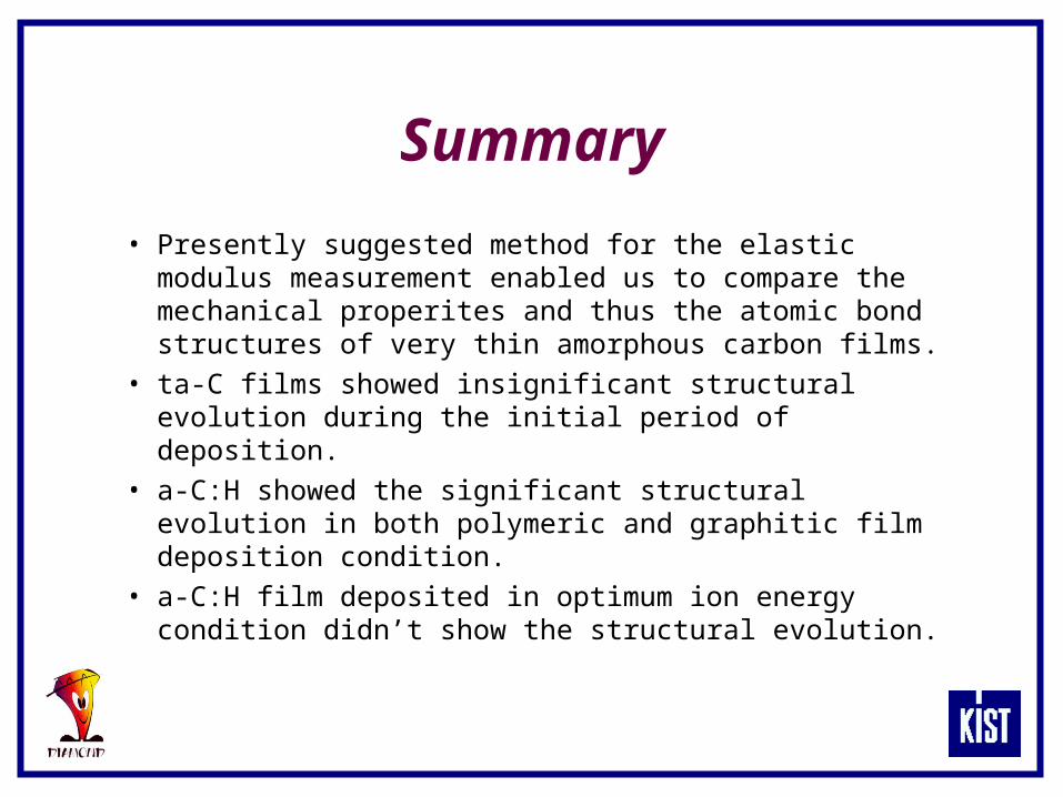
• Presently suggested method for the elastic modulus measurement enabled us to compare the mechanical properites and thus the atomic bond structures of very thin amorphous carbon films.
• ta-C films showed insignificant structural evolution during the initial period of deposition.
• a-C:H showed the significant structural evolution in both polymeric and graphitic film deposition condition.
• a-C:H film deposited in optimum ion energy condition didn’t show the structural evolution.

Applications of DLC Film
Related Documents