Comparative study of the mechanical properties of nanostructured thin films on stretchable substrates S. Djaziri, P.-O. Renault, E. Le Bourhis, Ph. Goudeau, D. Faurie, G. Geandier, C. Mocuta, and D. Thiaudière Citation: Journal of Applied Physics 116, 093504 (2014); doi: 10.1063/1.4894616 View online: http://dx.doi.org/10.1063/1.4894616 View Table of Contents: http://scitation.aip.org/content/aip/journal/jap/116/9?ver=pdfcov Published by the AIP Publishing Articles you may be interested in Deformation and fracture behavior of composite structured Ti-Nb-Al-Co(-Ni) alloys Appl. Phys. Lett. 104, 071905 (2014); 10.1063/1.4865930 Microstructure and mechanical properties of Ti–B–C–N–Si nanocomposite films deposited by unbalanced magnetron sputtering J. Vac. Sci. Technol. A 31, 061401 (2013); 10.1116/1.4815952 Microlattices as architected thin films: Analysis of mechanical properties and high strain elastic recovery APL Mat. 1, 022106 (2013); 10.1063/1.4818168 Mechanisms of reversible stretchability of thin metal films on elastomeric substrates Appl. Phys. Lett. 88, 204103 (2006); 10.1063/1.2201874 High ductility of a metal film adherent on a polymer substrate Appl. Phys. Lett. 87, 161910 (2005); 10.1063/1.2108110 [This article is copyrighted as indicated in the article. Reuse of AIP content is subject to the terms at: http://scitation.aip.org/termsconditions. Downloaded to ] IP: 194.254.166.120 On: Wed, 10 Sep 2014 08:54:03

Welcome message from author
This document is posted to help you gain knowledge. Please leave a comment to let me know what you think about it! Share it to your friends and learn new things together.
Transcript

Comparative study of the mechanical properties of nanostructured thin films onstretchable substratesS. Djaziri, P.-O. Renault, E. Le Bourhis, Ph. Goudeau, D. Faurie, G. Geandier, C. Mocuta, and D. Thiaudière
Citation: Journal of Applied Physics 116, 093504 (2014); doi: 10.1063/1.4894616 View online: http://dx.doi.org/10.1063/1.4894616 View Table of Contents: http://scitation.aip.org/content/aip/journal/jap/116/9?ver=pdfcov Published by the AIP Publishing Articles you may be interested in Deformation and fracture behavior of composite structured Ti-Nb-Al-Co(-Ni) alloys Appl. Phys. Lett. 104, 071905 (2014); 10.1063/1.4865930 Microstructure and mechanical properties of Ti–B–C–N–Si nanocomposite films deposited by unbalancedmagnetron sputtering J. Vac. Sci. Technol. A 31, 061401 (2013); 10.1116/1.4815952 Microlattices as architected thin films: Analysis of mechanical properties and high strain elastic recovery APL Mat. 1, 022106 (2013); 10.1063/1.4818168 Mechanisms of reversible stretchability of thin metal films on elastomeric substrates Appl. Phys. Lett. 88, 204103 (2006); 10.1063/1.2201874 High ductility of a metal film adherent on a polymer substrate Appl. Phys. Lett. 87, 161910 (2005); 10.1063/1.2108110
[This article is copyrighted as indicated in the article. Reuse of AIP content is subject to the terms at: http://scitation.aip.org/termsconditions. Downloaded to ] IP:
194.254.166.120 On: Wed, 10 Sep 2014 08:54:03
Comparative study of the mechanical properties of nanostructured thin filmson stretchable substrates
S. Djaziri,1,2 P.-O. Renault,2 E. Le Bourhis,2 Ph. Goudeau,2,a) D. Faurie,3 G. Geandier,4
C. Mocuta,5 and D. Thiaudiere5
1Max-Planck-Institut f€ur Eisenforschung GmbH, Max-Planck-Straße 1, 40237 D€usseldorf, Germany2Institut P’ (UPR 3346 CNRS), Universit�e de Poitiers, ENSMA, Bd Pierre et Marie Curie,86962 Futuroscope Cedex, France3LSPM, (UPR 3407 CNRS), Universit�e Paris 13, Institut Galil�ee, 99 avenue Jean-Baptiste Cl�ement,93430 Villetaneuse, France4Institut Jean Lamour (UMR 3079 CNRS), Universit�e de Lorraine, Parc de Saurupt, CS 50840,54011 NANCY Cedex, France5Synchrotron SOLEIL, L’Orme des Merisiers, Saint-Aubin, BP 48, 91192 Gif-sur-Yvette Cedex, France
(Received 5 July 2014; accepted 22 August 2014; published online 4 September 2014)
Comparative studies of the mechanical behavior between copper, tungsten, and W/Cu
nanocomposite based on copper disperso€ıd thin films were performed under in-situ controlled
tensile equi-biaxial loadings using both synchrotron X-ray diffraction and digital image correlation
techniques. The films first deform elastically with the lattice strain equal to the true strain given by
digital image correlation measurements. The Cu single thin film intrinsic elastic limit of 0.27% is
determined below the apparent elastic limit of W and W/Cu nanocomposite thin films, 0.30% and
0.49%, respectively. This difference is found to be driven by the existence of as-deposited residual
stresses. Above the elastic limit on the lattice strain-true strain curves, we discriminate two differ-
ent behaviors presumably footprints of plasticity and fracture. The Cu thin film shows a large tran-
sition domain (0.60% true strain range) to a plateau with a smooth evolution of the curve which is
associated to peak broadening. In contrast, W and W/Cu nanocomposite thin films show a less
smooth and reduced transition domain (0.30% true strain range) to a plateau with no peak broaden-
ing. These observations indicate that copper thin film shows some ductility while tungsten/copper
nanocomposites thin films are brittle. Fracture resistance of W/Cu nanocomposite thin film is
improved thanks to the high compressive residual stress and the elimination of the metastable b-W
phase. VC 2014 AIP Publishing LLC. [http://dx.doi.org/10.1063/1.4894616]
I. INTRODUCTION
The studies of the mechanical behavior of nanocomposite
thin films are of great interest not only because of their wide
technological applications but also because they offer the op-
portunity for studying the relation between the microstructural
length scale and the mechanical properties.1 In particular,
nanostructured metal thin films on polymer substrates are in
use in many technological applications, such as flexible elec-
tronics2 and polymer metallization.3 In aeronautics, metal/
polymer composites are very interesting thanks to their me-
chanical flexibility, light weight, and low thickness. This kind
of composites shows a larger strain at failure than freestanding
metal film.4,5 Moreover, the combination of different materi-
als in the form of nanolayered systems is known to improve
the mechanical properties of thin coatings.6 These systems
may show interesting electronic, optical, and magnetic proper-
ties.7–9 Combinations of the high thermal conductivity of cop-
per (Cu) and the low thermal expansion coefficient of
tungsten (W) makes W-Cu composites attractive for thermal
management applications.10 In addition to their electrical
properties, these metal composites present interesting me-
chanical strength resulting from the compromise between the
high strength of W and the ductility of Cu.11
The continuing trend of miniaturization in thin film
technology poses tremendous challenges for studying defor-
mation mechanisms at small scales. Indeed, when compared
with bulk counterparts the deformation mechanisms of nano-
structured materials are different.12,13 The size effects on the
plasticity of nanostructured materials have been extensively
studied over the past decade and although there is no funda-
mental understanding of deformation mechanisms, there is a
general agreement that the size effect manifests when film
thickness and/or grain size are smaller than 100 nm.14–16 At
this scale, deformation mechanisms based on grain bounda-
ries deformation processes come into play.12,17 Such tend-
ency has been observed for nanocrystalline films18–20 and
nanoscale multilayer films.21,22 Most of the previous studies
were conducted using conventional methods such as nanoin-
dentation and uniaxial tensile testing which do not reflect the
real thermo-mechanical loading that the thin-film undergoes
during preparation and in use. Mechanical testing under con-
trolled biaxial tension allows to overcome the limitations of
representative deformation modes. This has been achieved
thanks to the biaxial tensile device operating at room temper-
ature at DiffAbs beamline of the French synchrotron
a)Author to whom correspondence should be addressed. Electronic mail:
[email protected]. Tel.: þ33 549 496 726. Fax: þ33 549
496 692.
0021-8979/2014/116(9)/093504/8/$30.00 VC 2014 AIP Publishing LLC116, 093504-1
JOURNAL OF APPLIED PHYSICS 116, 093504 (2014)
[This article is copyrighted as indicated in the article. Reuse of AIP content is subject to the terms at: http://scitation.aip.org/termsconditions. Downloaded to ] IP:
194.254.166.120 On: Wed, 10 Sep 2014 08:54:03

radiation facility SOLEIL.23 Combined strain measurements
approach has been applied using X-ray diffraction (XRD)
and digital image correlation (DIC) in order to accurately
characterize the early stages of the mechanical deformation
of nanostructured thin films.24 It has been shown that the de-
formation is transmitted unchanged through the metal film/
polyimide substrate interface even for two materials with
such a high mechanical contrast and where the interface mor-
phology plays an important role on the physical properties of
coatings.25,26 A previous study of gold thin film on Kapton
substrate has also confirmed the complete strain transfer
through the film-substrate interface where the elastic
responses of both film and substrate have been measured
using synchrotron XRD.27
This paper presents a study on the mechanical properties
of three types of thin films deposited on polyimide sub-
strates: Cu single thin film, W single thin film, and W/Cu
nanocomposite based on quasi-isotropic copper disperso€ıdthin film. These three systems have been selected for study-
ing the role of grain size and microstructure as well as cop-
per addition on the ductile/brittle behavior of thin films. The
samples were subjected to equi-biaxial stress tension and
their obtained elastic limit was compared to each other.
II. SAMPLE DESIGN
A. Metal thin films
Thin films were deposited by sputtering method in the
central area of the cruciform polyimide substrate, in a 20 mm
diameter disk. Three series of samples were fabricated: Cu,
W, and W/Cu nanocomposite thin films. Sputtering deposi-
tion was performed at room temperature with an argon ion-
gun sputtering beam at 1.2 keV; the chamber base pressure
was 7� 10�5 Pa, and the working pressure during film
growth was 10�2 Pa. The deposition rate was approximately
of 0.05 and 0.07 nm/s for W and Cu layers, respectively. The
thin films were also deposited on 200 and 650 mm-thick
(001)-oriented Si wafers in order to characterize their corre-
sponding microstructure in the as-deposited configuration.
1. Pure Cu thin film
Pure Cu thin film was deposited with a total thickness of
200 6 10 nm. This value represents ten times the estimated
grain size (see below) and thus ensures to be over the perco-
lation threshold associated with the deposition process.
Texture analysis revealed that Cu thin film grains present
mainly an isotropic h111i fiber texture component.
The as-deposited Cu thin films are subject to a slight
tensile residual stress. The stress magnitude is about
þ100 MPa according to X-ray diffraction stress analysis (see
Table I). The average grain size estimated through Scherrer
approximation is about 20 nm.28
2. Pure W thin film
Pure W thin films were fabricated with a total thickness
of 150 6 10 nm. This value has been chosen to avoid thin
film delamination related to elastic energy release. Indeed,
increasing the film thickness increases the elastic energy
value due to the high compressive residual stress state in the
film (see below). Thin film buckling is observed over 150 nm
film thickness.29 Phase analysis by XRD measurements
shows that W crystallites exhibit two different phases: the
equilibrium pure W phase, called a-W which has a body-
centered cubic—bcc—structure (space group Im-3 m) and a
second one called b-W having an A15 cubic structure (space
group Pm-3n) which is stabilized by a low impurity (O, C)
concentration.30 The volume fraction of the b-W phase has
been estimated to be about 10% by the method given in Ref.
28. This method relies on comparing the integrated inten-
sities (or peak areas) of a a-W peak and a b-W peak.
W-scans (W being the angle between the normal to the
sample surface and the normal to the diffracting planes)
were performed on a-W{110}, a-W{200}, and a-W{211}
diffraction peaks in order to analyze crystallographic texture
of the a phase of W thin films. Also, several h-scans were
carried out in order to determine the crystallographic texture
of the b-W phase in the thin films. Texture analysis show
that the a-W grains exhibit mainly two fiber texture compo-
nents: a-W h110i and a-W h111i, while the b-W grains are
found to be oriented along b-W h100i fiber texture axis.
From calculations using Scherrer approximation, the size of
the a-W grains is estimated to be about 7 nm.
The as-deposited W thin films are subjected to high com-
pressive residual stresses of about �3.0 6 0.2 GPa obtained
by X-ray diffraction stress analysis in a-W phase (Table I).
3. W/Cu nanocomposite based on copper disperso€ıdsthin films
In order to better control the microstructure of W, W, and
Cu have been sputtered alternatively on the polyimide sub-
strate. The effective thicknesses of W and Cu are 3.2 6 0.1 nm
and 0.6 6 0.1 nm, respectively. The thin film was fabricated
with 38 periods which leads to a total thickness of about
TABLE I. Microstructure of the studied thin films deposited on Kapton substrates: K, ti, and rri correspond to period, thickness, and residual stress, respec-
tively, associated to subscript i (W, Cu, or f). W or Cu refers, respectively, to tungsten or copper component and f to the film. Residual stresses in W or Cu
component were determined by XRD measurements.
Effective thicknesses (nm) Crystallographic textures Residual stresses (GPa)
Thin film K tW tCu tf a-W b-W Cu rrW rr
Cu
W … 152 … 150 {111}þ {110} {100} … �3.0 …
Cu … … 221 200 … … {111} … 0.1
W/Cu 3.8 3.2 0.6 150 {110} … … �3.0 …
093504-2 Djaziri et al. J. Appl. Phys. 116, 093504 (2014)
[This article is copyrighted as indicated in the article. Reuse of AIP content is subject to the terms at: http://scitation.aip.org/termsconditions. Downloaded to ] IP:
194.254.166.120 On: Wed, 10 Sep 2014 08:54:03

150 6 10 nm. Due to the introduction of Cu, W crystallites ex-
hibit only one phase: the equilibrium a-W phase and present
only the a-W h110i fiber texture component. The unique a-W
h110i texture component is obtained from a thickness thresh-
old of Cu determined at 0.6 nm.31 Energy-dispersive X-ray
spectroscopy was used in a scanning electron microscope in
order to determine the atomic concentrations of Cu and W in
the film. The volume fraction of the Cu phase has been esti-
mated to be about 20% of the global thin film volume. The
microstructural morphology of the nanocomposite thin film
was characterized by grazing incidence small angle X-ray
scattering (GISAXS). The analysis of the GISAXS patterns
shows that the thin film can be represented as an arrangement
of Cu nanoaggregates within a W matrix. The Cu clusters are
ellipsoidal with an average diameter close to 5 nm. The calcu-
lated grain size of a-W phase using Scherrer’s formula is also
about 5 nm. However, the diffracting signal from Cu nanoag-
gregates in W/Cu thin films is too weak to allow an accurate
analysis of copper in grain strains.
The W crystallites are subject to a high compressive re-
sidual stresses of about �3.0 6 0.2 GPa obtained by X-ray
diffraction stress analysis in a-W phase (Table I). This value
is equal to the one found for the a-W phase in a pure W thin
film. Then, the number of period has been fixed in order to
reach a total thickness slightly lower than the one of pure W
films (see previous paragraph).
B. Polyimide substrate
The sample structure consists of a cruciform polyimide
substrate coated by a metallic thin film. The substrate acts as
a mechanical support and provides a stronger constraint on
thin film cracking due to its stiffness.32
The metal thin film/compliant substrate structure poses
greater challenges for the development of flexible and
stretchable devices. In order to accurately determine the me-
chanical behavior of such structures in service, it is of utmost
importance to account for the realistic complex stress condi-
tions. To address these tasks, biaxial tests were carried out
using cruciform shape substrate loaded in biaxial device.
The substrate geometry has been optimized using finite
element modeling to obtain homogeneous stress condition on
a few square millimeters of the deposited area.33 Indeed, this
is crucial for the XRD measurements. The chosen substrate is
a KaptonVR
HN from DuPontTM with 125 lm thickness,
20-mm wide arms, and a 5-mm toe weld. The substrates were
ultrasonically cleaned with acetone before deposition.
III. MECHANICAL TEST AND STRAINMEASUREMENTS
The biaxial tensile experiments were performed using
the biaxial tensile device dedicated to DiffAbs beamline at
the French synchrotron radiation source SOLEIL. The exper-
imental setup is illustrated and described elsewhere.23,24 All
in-situ tensile tests were conducted using a step by step load-
ing procedure. The value of the applied load is given by the
load cell for each loading step; the corresponding applied
stress for a load of 100 N is 39 MPa based on the sample
geometry. XRD and DIC measurements were performed to
measure the lattice and true strains, respectively.
A. Lattice strain
The high intensity of the synchrotron radiation and the
use of a hybrid pixel detector (XPAD3.1) allowed the mea-
surement of the lattice strain into thin films in short counting
times with good accuracy.34 Sin2W measurements have been
performed for one azimuthal angle only (U¼ 0� being arbi-
trary fixed for one of the two cross line of the cruciform kap-
ton substrate), since the applied loadings were equi-biaxial.
Bragg peak profiles were obtained by azimuthal integration
of the partial Debye-Scherrer rings.35 Pearson VII function
and linear background have been used to fit the diffraction
diagram in order to extract the 2h peak position as well as
the peak broadening during deformation. The lattice strain
feghkl0W corresponding to {hkl} diffracting planes and a scat-
tering vector with (0,W) orientation has been obtained using
the following equation:
ef ghkl0W ¼
d0W � dð0Þ0W
dð0Þ0W
¼ lnd0W
dð0Þ0W
!¼ ln
sin h 0ð Þ0W
sin h0W
!
¼ e11 � e33ð Þ sin2Wþ e33; (1)
where dð0Þ0W is the reference lattice spacing, and hð0Þ0W the asso-
ciated reference diffraction angle which corresponds here to
the unloaded state. d0W and h0W are the lattice spacing and
the diffraction angle, respectively, for the loaded states. e11
and e33 correspond to in-plane and out-of-plane strains,
respectively.
The evolution of the peak width was used to address the
deformation mechanisms underlying the mechanical behav-
ior of the thin films. The biaxial stresses in thin films during
deformation were determined from the measured X-ray elas-
tic strains.36 In the current study, the monochromatic X-ray
beam energy was 8.8 keV. The focal point was at the center
of the 6-circle diffractometer (corresponding to the sample
position) with 0.3 lm in size (same value in both directions).
Experimental details can be found in Ref. 24.
B. True strain
The true strain of the samples was obtained by meas-
uring the displacement of speckle dots spray-painted on the
rear surface of the polyimide substrate, employing the opti-
cal camera of the testing device which looks at the rear face
of the sample. The size of the captured region of the sample
surface is 9� 6.3 mm2 and corresponds to the size of the uni-
formly strained zone as predicted by finite element calcula-
tions. DIC analysis was used to track the evolution of the
deformation of the polyimide substrate during the tensile
test.37 The DIC method is based on the conservation of the
gray level between two images
f ðxÞ ¼ g ½xþ �uðxÞ�; (2)
where g(x) and f(x) are gray level functions corresponding to
the reference and deformed image configurations at each
093504-3 Djaziri et al. J. Appl. Phys. 116, 093504 (2014)
[This article is copyrighted as indicated in the article. Reuse of AIP content is subject to the terms at: http://scitation.aip.org/termsconditions. Downloaded to ] IP:
194.254.166.120 On: Wed, 10 Sep 2014 08:54:03
pixel point of coordinate x. �u is the displacement field in the
measured direction.
The true strain is determined in terms of displacement
field, considering small strains and very small rotations
�eij ¼1
2
@�ui
@jþ @�uj
@i
� �; (3)
where (i,j)¼ (x,y), and �ui and �uj are displacement
components.
The results of preliminary experiments combining the
two techniques show that the two strains are measured with
accuracy better than 10�4 in the elastic domain for various
loading paths.24 It is worth noting that the strains reported
herein are very small and typically less than 1.8%.
IV. RESULTS
A. Pure Cu thin film
During the tensile test of pure Cu thin film, equi-biaxial
loadings ranging from 14 to 170 N have been applied to the
film/substrate composite. Only the {220}-planes of Cu have
been monitored from XRD measurements. These (hkl)
planes are selected to fit the following perquisites which are
reliable determination of strains: peak intensity and position
toward large diffraction angle, X-ray elastic constants close
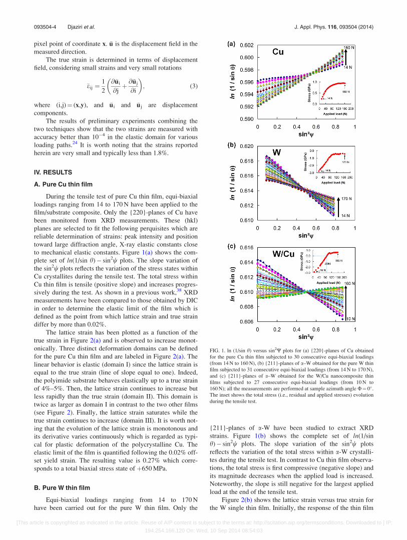
to mechanical elastic constants. Figure 1(a) shows the com-
plete set of ln(1/sin h)� sin2w plots. The slope variation of
the sin2w plots reflects the variation of the stress states within
Cu crystallites during the tensile test. The total stress within
Cu thin film is tensile (positive slope) and increases progres-
sively during the test. As shown in a previous work,38 XRD
measurements have been compared to those obtained by DIC
in order to determine the elastic limit of the film which is
defined as the point from which lattice strain and true strain
differ by more than 0.02%.
The lattice strain has been plotted as a function of the
true strain in Figure 2(a) and is observed to increase monot-
onically. Three distinct deformation domains can be defined
for the pure Cu thin film and are labeled in Figure 2(a). The
linear behavior is elastic (domain I) since the lattice strain is
equal to the true strain (line of slope equal to one). Indeed,
the polyimide substrate behaves elastically up to a true strain
of 4%–5%. Then, the lattice strain continues to increase but
less rapidly than the true strain (domain II). This domain is
twice as larger as domain I in contrast to the two other films
(see Figure 2). Finally, the lattice strain saturates while the
true strain continues to increase (domain III). It is worth not-
ing that the evolution of the lattice strain is monotonous and
its derivative varies continuously which is regarded as typi-
cal for plastic deformation of the polycrystalline Cu. The
elastic limit of the film is quantified following the 0.02% off-
set yield strain. The resulting value is 0.27% which corre-
sponds to a total biaxial stress state of þ650 MPa.
B. Pure W thin film
Equi-biaxial loadings ranging from 14 to 170 N
have been carried out for the pure W thin film. Only the
{211}-planes of a-W have been studied to extract XRD
strains. Figure 1(b) shows the complete set of ln(1/sin
h)� sin2w plots. The slope variation of the sin2w plots
reflects the variation of the total stress within a-W crystalli-
tes during the tensile test. In contrast to Cu thin film observa-
tions, the total stress is first compressive (negative slope) and
its magnitude decreases when the applied load is increased.
Noteworthy, the slope is still negative for the largest applied
load at the end of the tensile test.
Figure 2(b) shows the lattice strain versus true strain for
the W single thin film. Initially, the response of the thin film
FIG. 1. ln (1/sin h) versus sin2W plots for (a) {220}-planes of Cu obtained
for the pure Cu thin film subjected to 30 consecutive equi-biaxial loadings
(from 14 N to 160 N), (b) {211}-planes of a–W obtained for the pure W thin
film subjected to 31 consecutive equi-biaxial loadings (from 14 N to 170 N),
and (c) {211}-planes of a–W obtained for the W/Cu nanocomposite thin
films subjected to 27 consecutive equi-biaxial loadings (from 10 N to
160 N); all the measurements are performed at sample azimuth angle U¼ 0�.The inset shows the total stress (i.e., residual and applied stresses) evolution
during the tensile test.
093504-4 Djaziri et al. J. Appl. Phys. 116, 093504 (2014)
[This article is copyrighted as indicated in the article. Reuse of AIP content is subject to the terms at: http://scitation.aip.org/termsconditions. Downloaded to ] IP:
194.254.166.120 On: Wed, 10 Sep 2014 08:54:03

(lattice strain) is linear elastic (domain I) as it is equal to the
polyimide substrate response (true strain). Then, the lattice
strain is no longer equal to the true strain but less than the
true strain (domain II). Within this domain, the lattice strain
continues to increase with a change on the slope of the curve
less smooth than for Cu film. Finally, the lattice strain satu-
rates while the true strain continues to increase (domain III).
It is worth noting that domain II is about half that observed
for Cu. Both this reduced excursion and the less smooth evo-
lution are attributed to brittle behavior. Moreover, the disper-
sion of data in the plateau of the domain III confirms this
result. The elastic limit of the film is quantified following the
0.02% offset yield strain. The resulting value is 0.30% which
corresponds to a total compressive biaxial stress state of
�1.7 6 0.4 GPa (applied stress of 1.3 GPa) in a-W crystalline
phase.
C. W/Cu nanocomposite based on copper disperso€ıdsthin films
During this test, equi-biaxial loadings ranging from 10
to 160 N have been applied to the film/substrate composite.
Only the {211}-planes of a-W have been studied by
XRD measurements. Figure 1(c) shows the complete set of
ln(1/sin h)� sin2w plots. Considering this case of a nano-
structured W thin film, the total stress within a-W crystallites
is first compressive as for the W single thin film and
decreases when the applied load is increased. However, the
stress becomes tensile from an applied load of 89 N approxi-
mately which is in contrast with the pure W thin film me-
chanical behavior shown above.
The lattice strain has been plotted as a function of the
true strain in Figure 2(c) where the three deformation
domains are labelled and defined as shown for the W single
thin film. The elastic limit of the film is found at 0.49% fol-
lowing the 0.02% offset yield strain criterion. The resulting
value corresponds to a total compressive stress of about
�0.4 GPa (applied stress of þ2.9 GPa) in a-W crystalline
phase.
V. DISCUSSION
The method used in the present study allows for a
straightforward and reliable determination of the elastic limit
of thin film composites thanks to combined measurements
by synchrotron XRD and DIC techniques. The studied sam-
ples show obviously three distinct deformation regimes as
observed in previous studies of metal thin films.38–41
The elastic domain was followed by energy dissipation
in the film volume as the film/substrate composite was fur-
ther strained until saturation (plateau stress). The obtained
elastic limit for each coating is determined in view of the
microstructure and it is clear that the combination of W and
Cu in the form of a nanostructured composite resulted in an
improved elastic limit. Changes in both coating elastic stress
and peak broadening during loading reveal different defor-
mation mechanisms which will be discussed in the light of
these two parameters.
It should be noted that all the samples were subjected to
the same applied strain conditions which were governed by
FIG. 2. Lattice strain as a function of true strain for (a) pure Cu thin film,
(b) pure W thin film, and (c) W/Cu nanocomposite thin films. The red straight
line has the slope equal to one, e being the x-ray strain and �e the true strain.
FIG. 3. True strain determined by DIC in the Kapton substrate vs. the
applied load for the different studied coatings (W, Cu, and W/Cu thin films).
093504-5 Djaziri et al. J. Appl. Phys. 116, 093504 (2014)
[This article is copyrighted as indicated in the article. Reuse of AIP content is subject to the terms at: http://scitation.aip.org/termsconditions. Downloaded to ] IP:
194.254.166.120 On: Wed, 10 Sep 2014 08:54:03

the mechanical properties of the substrate. As shown in
Figure 3, the obtained true strain in the Kapton substrate is
similar for the different coatings. This demonstrates the very
good repeatability of the measurements.
We investigated and compared the deformation modes
of each coating. Figure 4 shows the stress-strain curves of
each sample; two types of behavior are highlighted. Let us
notice that the stress values have been calculated from the
slopes of the curves in Figure 1 taking into account the bulk
elastic constants of copper and tungsten.42 The evolution of
stress in the Cu thin film is monotonous with a large transi-
tion domain II which is representative of a ductile material.
In the present case, the Cu thin film behaves elastically up to
an applied strain of about 0.27% in accordance with the line-
arity of the stress-strain behavior. In Figure 6, we plotted the
relative evolution of the diffraction peak width as a function
of the true strain. For the Cu thin film, the peak width
increases slightly within the elastic domain (domain I) which
may be due to the elastic anisotropy inducing elastic strain
heterogeneities.43 In transition domain II (between 0.27%
and 0.75% applied strain), both the stress and the peak width
increase indicating strain hardening effects. In domain III
(beyond 0.75% applied strain), the stress becomes constant
and the peak width increases less strongly with the applied
strain. The peak broadening is usually attributed to an
increased dislocation density and an inhomogeneous plastic
deformation. The present study concerns Cu thin film with a
grain size of about 20 nm. The investigation of the stress-
strain behavior reveals a reduced strain hardening and a
near-perfect plastic behavior of the Cu film. This is in good
agreement with the observations in Ref. 44 for nanocrystal-
line Cu of grain size between 50 and 80 nm. These results
may indicate that the dislocation activity is reduced and plas-
tic deformation is dominated by diffusional grain-boundary
sliding as it has been extensively reported for nanocrystalline
cubic metals with grain size below 40 nm.17,45–48
As shown in Sec. IV A, the evolution of elastic stress as
function of true strain is monotonous in a large transition do-
main (labelled II in Fig. 2). This may be interpreted as evi-
dence that the Cu thin film undergoes some ductility. Such
results have also been observed for similar composites of Cu
thin film-polyimide substrate.49,50
By contrast, the W thin film and the W/Cu nanocompo-
site thin film show a brittle behavior as revealed by the varia-
tion of the x-ray stress (Figure 4) and the peak width (Figure
5) versus the true strain. The stress-strain curves of these
films can also be divided into three deformation domains.
The first domain (I) corresponds to an elastic deformation as
indicated by the linear stress-strain relationship and a con-
stant peak width (up to 0.30% and 0.49% applied strain for
W thin film and W/Cu nanocomposite thin film, respec-
tively). By increasing the strain, the elastic stress increases
less rapidly in the second domain (II) and becomes constant
in the third domain (III). It is worth noting that, in contrast to
Cu, the peak width is almost constant during the entire ten-
sile test for the W thin film (it slightly decreases in domains
II and III for the W/Cu nanocomposite thin film).
Furthermore, the stress plateau in the domain III of these two
thin films shows a slight dispersion of data. The less smooth
variation of stress within the reduced domain II is attributed
to two competing processes: thin film cracking with an
increased crack density versus a continued elastic
FIG. 4. Variation of the x-ray stress as a function of the true strain for the
pure Cu thin film, the pure W thin film, and the W/Cu nanocomposite thin
films. The horizontal dotted line marks the zero stress level. Arrows indicate
the total stress (i.e., residual and applied stresses) for each film at yielding at
0.02% strain offset.
FIG. 6. ln (1/sin h) versus sin2W plots for {321}-planes of b–W obtained for
the pure W thin film subjected to equi-biaxial loadings (only three loadings
are presented); the measurements are performed at sample azimuth angle
U¼ 0�.
FIG. 5. Relative evolution of the peak width as a function of the true strain
for the Cu single thin film, the W single thin film, and the W/Cu nanocompo-
site thin films as a function of the true strain. Only diffraction data of {220}-
planes of Cu and {211}-planes of W are reported here. The horizontal dotted
line marks the reference level.
093504-6 Djaziri et al. J. Appl. Phys. 116, 093504 (2014)
[This article is copyrighted as indicated in the article. Reuse of AIP content is subject to the terms at: http://scitation.aip.org/termsconditions. Downloaded to ] IP:
194.254.166.120 On: Wed, 10 Sep 2014 08:54:03

deformation of the adherent parts of the film as the applied
strain is increased. The less rapid and smooth stress evolu-
tion in those thin films is a signature of crack nucleation and
propagation as observed in Ref. 41 for Ta thin films on polyi-
mide substrates.40 However, the set-up did not allow surface
imaging of the coating surface to confirm cracking develop-
ment during tensile loading. Moreover, no cracks have been
observed during and after sample unloading. The relaxation
of the polyimide substrate may induce the shrinkage of the
sample and closure of cracks upon full unloading as
observed in copper films on Poly Ethylene Terephthalate
(PET) substrate.51
It is interesting to note that the elastic domain of the
W/Cu nanocomposite thin film is larger than that of the pure
W thin film. This is related to microstructural differences
between the two thin films where the presence of the b-W
phase in the pure W thin film has the main impact on the me-
chanical properties of the film. This is demonstrated by a
reduced fracture resistance (1.3 GPa) compared to that of the
W/Cu nanocomposite (2.9 GPa) where W crystallites exhibit
only the stable a-W phase. Indeed, the elastic stress in the
b-W phase is initially compressive and becomes tensile
before the crack initiation observed in the a-W phase as
shown from the ln(1/sin h)� sin2w plots in Figure 6. This
tensile state in the b-W phase induces the initiation of cracks
in the W thin film at lower strain (0.30%) although the a-W
phase is under a high compressive stress at this stage of de-
formation. In the case of the W/Cu nanocomposite thin film,
the a-W phase exhibits a unique h110i fiber texture compo-
nent and more interestingly the b-W phase is suppressed.
The microstructure change induced by the addition of a
given amount of Cu within the W matrix explains the
enhanced fracture resistance obtained for the nanocomposite
thin film. The onset of cracking is determined at larger strain
(0.49%) where the a-W phase is under a low compressive
stress of about �0.4 GPa. Noteworthy, the compressive re-
sidual stress may delay the crack initiation in the coating
subjected to tensile loading conditions and the coating failure
occurs when the stress is in the tensile regime.52–54
Furthermore, the presence of the Cu nanocrystalline phase
appears to improve the fracture resistance of the thin film.
Indeed, the addition of second phase inclusions can influence
the crack propagation as already observed in Ni embedded
alumina nanocomposite thin films.55 The observed improve-
ment could be explained by crack bridging mechanism,56,57
according to which, the particles, when approached by a
crack, form bridging zones behind the crack front. This
bridging ligament exerts closure stresses, which reduce the
stress intensity at the crack tip. The propagation of cracks,
initiated in a brittle phase, would be stopped by particles that
debond partially from the brittle matrix, thus absorbing
energy and bridging the crack. This would lead to a limited
crack growth.58,59 The high fraction of atoms that is present
at grain boundaries may hinder the motion of dislocations
for W and Cu with grain size on the nanometer range.17 We
therefore assume that the energy dissipation in the film is
due to microcracks generation as it has been confirmed
unambiguously in a previous paper,41 plotting the yield sur-
face of the W/Cu film using different proportional loading
paths. Interestingly, thin film failure occurs by different
modes when non-equibiaxial loadings are applied.60
According to Figure 2(c), the second domain of deforma-
tion for the pure Cu thin film is approximately twice as large
as those of pure W and W/Cu thin films. This significant dif-
ference is caused by the difference in deformation mecha-
nisms. The investigation of the Cu film response revealed
some plasticity. This should be the main reason for the large
deformation of the Cu thin film before saturation of the elastic
strain. It is interesting to note in Figure 4 that the Cu thin film
is initially under a slight tensile biaxial stress, which tends
towards a near zero stress state, whereas the W and W/Cu thin
films are initially under a high compressive biaxial stress
(�3.0 6 0.4 GPa). Therefore, the obtained elastic limit for the
Cu film represents an intrinsic property of the film contrary to
the W and W/Cu thin films which behaviors depend strongly
on the initial residual stress prior to deformation.
VI. CONCLUSION
Controlled biaxial tensile testing with combined strain
measurements using both synchrotron X-ray diffraction and
digital image correlation has been used to test three metallic
thin films: Cu thin film, W thin film, and W/Cu nanocomposite
based on quasi-isotropic copper disperso€ıds thin film. From the
analysis of the stress-strain curves and the peak width, we find
that the thin films behave elastically up to 0.27%, 0.30%, and
0.49% for Cu, W, and W/Cu, respectively. Because the Cu
thin film is initially close to a zero stress state, the obtained
elastic limit corresponds to an intrinsic property. In contrast,
the elastic limits of W and W/Cu thin films are determined by
the high as-deposited residual stress present in these films.
Above the elastic limit, the observations suggest two different
behaviors, namely, plasticity for the Cu thin film showing
20 nm grain size and fracture for W and W/Cu thin films where
the a-W grain size is about 5 nm. Indeed, the Cu thin film
shows a large transition domain to a plateau with a smooth
evolution of the stress-strain curve which is associated to a
peak broadening whereas, W and W/Cu thin films show a less
smooth and smaller transition domain to a plateau with no
peak broadening. The elastic limit of the W/Cu thin film is
�60% higher than that of the W thin film. This enhanced frac-
ture resistance of the W/Cu thin film is due to the change of
the microstructure that plays an important role on this property.
The presence of the high compressive residual stress and the
elimination of the metastable b-W phase are considered as
main factors for the improved mechanical behavior of the W/
Cu thin film.
ACKNOWLEDGMENTS
We acknowledge Yannick Diot and Philippe Gu�erin
from the PPRIME institute for samples preparation and
SOLEIL for provision of synchrotron radiation facilities.
This work was partially funded by the French Government
program “Investissements d’Avenir” (LABEX INTERACTIFS,
reference ANR-11-LABX-0017-01).
1M. A. Meyers, A. Mishra, and D. J. Benson, Prog. Mater. Sci. 51, 427
(2006).
093504-7 Djaziri et al. J. Appl. Phys. 116, 093504 (2014)
[This article is copyrighted as indicated in the article. Reuse of AIP content is subject to the terms at: http://scitation.aip.org/termsconditions. Downloaded to ] IP:
194.254.166.120 On: Wed, 10 Sep 2014 08:54:03

2S. P. Lacour, D. Chan, S. Wagner, T. Li, and Z. Suo, Appl. Phys. Lett. 88,
204103 (2006).3W. T. Li, R. B. Charters, B. Luther-Davies, and L. Mar, Appl. Surf. Sci.
233, 227 (2004).4T. Li, Z. Huang, Z. Suo, S. P. Lacour, and S. Wagner, Appl. Phys. Lett.
85, 3435 (2004).5J. Xiao, A. Carlson, Z. J. Liu, Y. Huang, H. Jiang, and J. A. Rogers, Appl.
Phys. Lett. 93, 013109 (2008).6P. A. Gruber, E. Arzt, and R. Spolenak, J. Mater. Res. 24, 1906 (2009).7X. Zhang, M. F. Hundley, A. Malinowski, A. Misra, H. Wang, and M.
Nastasi, J. Appl. Phys. 95, 3644 (2004).8A. Gurevich, Appl. Phys. Lett. 88, 012511 (2006).9Y. Wang, L. Y. Chen, S. M. Zhou, Y. X. Zheng, A. Hu, H. R. Zhai, R.
Naik, G. L. Dunifer, and G. W. Auner, J. Appl. Phys. 81, 5256 (1997).10A. Luedtke, Adv. Eng. Mater. 6, 142 (2004).11P. M. Geffroy, T. Chartier, and J. F. Silvain, Adv. Eng. Mater. 9, 547
(2007).12S. H. Oh, M. Legros, D. Kiener, P. Gruber, and G. Dehm, Acta Mater. 55,
5558 (2007).13G. Dehm, Prog. Mater. Sci. 54, 664 (2009).14A. Misra and H. Kung, Adv. Eng. Mater. 3, 217 (2001).15A. Misra, J. P. Hirth, and R. G. Hoagland, Acta Mater. 53, 4817 (2005).16J. R. Greer and J. T. M. De Hosson, Prog. Mater. Sci. 56, 654 (2011).17P. A. Gruber, J. B€ohm, F. Onuseit, A. Wanner, R. Spolenak, and E. Arzt,
Acta. Mater. 56, 2318 (2008).18Z. Budrovic, H. Van Swygenhoven, P. M. Derlet, S. Van Petegem, and B.
Schmitt, Science 304, 273 (2004).19X. Yu, J. Zhang, Y. Zhang, L. Wang, and Y. Zhao, J. Appl. Phys. 111,
113506 (2012).20G. Guisbiers, M.-S. Colla, M. Coulombier, J.-P. Raskin, and T. Pardoe,
J. Appl. Phys. 113, 024513 (2013).21S. Shao, H. M. Zbib, I. N. Mastorakos, and D. F. Bahr, J. Appl. Phys. 112,
044307 (2012).22J. J. Niu, J. Y. Zhang, G. Liu, P. Zhang, S. Y. Lei, G. J. Zhang, and J. Sun,
Acta. Mater. 60, 3677 (2012).23G. Geandier, D. Thiaudiere, R. N. Randriamazaoro, R. Chiron, S. Djaziri,
B. Lamongie, Y. Diot, E. Le Bourhis, P. O. Renault, P. Goudeau, A.
Bouaffad, O. Castelnau, D. Faurie, and F. Hild, Rev. Sci. Instrum. 81,
103903 (2010).24S. Djaziri, P.-O. Renault, F. Hild, E. Le Bourhis, Ph. Goudeau, D.
Thiaudiere, and D. Faurie, J. Appl. Cryst. 44, 1071 (2011).25G. Palasantzas and J. Th. M. De Hosson, J. Appl. Phys. 93, 320 (2003).26T. H€ochbauer, A. Misra, K. Hattar, and R. G. Hoagland, J. Appl. Phys. 98,
123516 (2005).27G. Geandier, P.-O. Renault, E. Le Bourhis, Ph. Goudeau, D. Faurie, C. Le
Bourlot, Ph. Dj�emia, O. Castelnau, and S. M. Ch�erif, Appl. Phys. Lett. 96,
041905 (2010).28P. Villain, P. Goudeau, J. Ligot, S. Benayoun, K. F. Badawi, and J.-J.
Hantzpergue, J. Vac. Sci. Technol., A 21, 967 (2003).29P. Goudeau, P. Villain, N. Tamura, and H. A. Padmore, Appl. Phys. Lett.
83, 51 (2003).30B. Girault, D. Eyidi, P. Goudeau, T. Sauvage, P. Guerin, E. Le Bourhis,
and P.-O. Renault, J. Appl. Phys. 113, 174310 (2013).31B. Girault, D. Eyidi, T. Chauveau, D. Babonneau, P. O. Renault, E. Le
Bourhis, and P. Goudeau, J. Appl. Phys. 109,014305 (2011).32N. Lu, X. Wang, Z. Suo, and J. Vlassak, Appl. Phys. Lett. 91, 221909
(2007).
33S. Djaziri, D. Thiaudiere, G. Geandier, P.-O. Renault, E. Le Bourhis, P.
Goudeau, O. Castelnau, and D. Faurie, Surf. Coat. Technol. 205, 1420
(2010).34K. Medjoubi, T. Bucaille, S. Hustache, J.-F. B�erar, N. Boudet, J.-C.
Clemens, P. Delpierre, and B. Dinkespiler, J. Synchrotron Radiat. 17, 486
(2010).35C. Le Bourlot, P. Landois, S. Djaziri, P. O. Renault, E. Le Bourhis, P.
Goudeau, M. Pinault, M. Mayne-L’Hermite, B. Bacroix, D. Faurie, O.
Castelnau, P. Launois, and S. Rouziere, J. Appl. Crystallogr. 45, 38
(2012).36D. Faurie, P. Djemia, E. Le Bourhis, P. O. Renault, Y. Roussign�e, S. M.
Ch�erif, R. Brenner, O. Castelnau, G. Patriarche, and Ph. Goudeau, Acta.
Mater. 58, 4998 (2010).37G. Besnard, F. Hild, and S. Roux, Exp. Mech. 46, 789 (2006).38S. Djaziri, D. Faurie, E. Le Bourhis, Ph. Goudeau, P.-O. Renault, C.
Mocuta, D. Thiaudiere, and F. Hild, Thin Solid Films 530, 30 (2013).39S. Van Petegem, L. Li, P. M. Anderson, and H. Van Swygenhoven, Thin
Solid Films 530, 20 (2013).40S. Frank, U. A. Handge, S. Olliges, and R. Spolenak, Acta. Mater. 57,
1442 (2009).41S. Djaziri, D. Faurie, P.-O. Renault, E. Le Bourhis, Ph. Goudeau, G.
Geandier, and D. Thiaudiere, Acta. Mater. 61, 5067 (2013).42V. Hauk, Structural and Residual Stress Analysis by Non Destructive
Methods: Evaluation, Application, Assessment (Elsevier, Amsterdam,
1997).43F. Siska, S. Forest, and P. Gumbsch, Comput. Mater. Sci. 39, 137
(2007).44Y. Champion, C. Langlois, S. Gu�erin-Mailly, P. Langlois, J. L.
Bonnentien, and M. J. H€ytch, Science 300, 310 (2003).45H. V. Swygenhoven, Science 296, 66 (2002).46J. Schiotz and K. W. Jacobsen, Science 301, 1357 (2003).47M. Chen, E. Ma, K. J. Hemker, H. Sheng, Y. Wang, and X. Cheng,
Science 300, 1275 (2003).48X. Z. Liao, Y. H. Zhao, S. G. Srinivasan, Y. T. Zhua, R. Z. Valiev, and D.
V. Gunderov, Appl. Phys. Lett. 84, 592 (2004).49M. Hommel and O. Kraft, Acta. Mater. 49, 3935 (2001).50D. S. Gianola, S. Van Petegem, M. Legros, S. Brandstetter, H. Van
Swygenhoven, and K. J. Hemker, Acta. Mater. 54, 2253 (2006).51O. Glushko, V. M. Marx, C. Kirchlechner, I. Zizak, and M. J. Cordill,
Thin Solid Films 552, 141 (2014).52F. Ahmed, K. Bayerlein, S. M. Rosiwal, M. G€oken, and K. Durst, Acta.
Mater. 59, 5422 (2011).53C. C. Aydıner, D. W. Brown, A. Misra, N. A. Mara, Y.-C. Wang, J. J.
Wall, and J. Almer, J. Appl. Phys. 102, 083514 (2007).54C. C. Aydıner, D. W. Brown, N. A. Mara, J. Almer, and A. Misra, Appl.
Phys. Lett. 94, 031906 (2009).55S. Neralla, D. Kumar, S. Yarmolenko, and J. Sankar, Composites: Part B
35, 157 (2004).56B. Budiansky, J. C. Amazigo, and A. G. Evans, J. Mech. Phys. Solids 36,
167 (1988).57L. S. Sigl, P. A. Mataga, B. J. Dalgleish, R. M. McMeeking, and A. G.
Evans, Acta Metall. 36, 945 (1988).58J. Y. Zhang, G. Liu, X. Zhang, G. J. Zhang, J. Sun, and E. Ma, Scr. Mater.
62, 333 (2010).59L. Liu and X. Chen, Acta. Mater. 56, 6214 (2008).60P.-O. Renault, E. Le Bourhis, Ph. Goudeau, D. Thiaudiere, and D. Faurie,
Thin Solid Films 549, 239 (2013).
093504-8 Djaziri et al. J. Appl. Phys. 116, 093504 (2014)
[This article is copyrighted as indicated in the article. Reuse of AIP content is subject to the terms at: http://scitation.aip.org/termsconditions. Downloaded to ] IP:
194.254.166.120 On: Wed, 10 Sep 2014 08:54:03
Related Documents