International Journal on Cybernetics & Informatics (IJCI) Vol. 5, No. 4, August 2016 DOI: 10.5121/ijci.2016.5428 255 COMPARATIVE PERFORMANCE ANALYSIS OF LOW POWER FULL ADDER DESIGN IN DIFFERENT LOGICS IN 22nm SCALING TECHNOLOGY A.Murali 1 , L.V.Santosh Kumar Y 2 and P.Rajesh 3 1 Associate Professor, Member IEEE, Department of Electronics and Communication Engineering & Research Scholar, Department of ECE, KLEF, K.L University, Green Fields, Guntur, A.P, India 2,3 Assistant Professor, Department of Electronics and Communication Engineering 1,2,3 Raghu Engineering College, Visakhapatnam, A.P, India ABSTRACT This paper gives the comparison of performance of full adder design in terms of area, power and delay in different logic styles. Full adder design achieves low power using the Transmission Gate logic compared to all other topologies such as Basic CMOS, Pass Transistor and GDI techniques but it make use of more number of transistors compared to GDI. GDI occupies less area compared to all other logic design styles. This paper presents the simulated outcome using Tanner tools and also H-Spice tool which shows power and speed comparison of different full adder designs. All simulations have been performed in 90nm, 45nm and 22nm scaling parameters using Predictive Technology Models in H-Spice tool. KEYWORDS CMOS, SGMOSFET, DGMOSFET, Transmission Gate, GDI, Predictive Technology. 1. INTRODUCTION To reduce the size of chip, the complexity in the circuits has increased drastically, because of that the power dissipation and performance of the circuit are being affected. So, there is concern towards circuits design in low power VLSI design to reduce the chip area and power dissipation [1]. There are two types of power dissipations in MOSFET, namely static power dissipation and dynamic power dissipation. In Static power dissipation, there are few parameters which show effect on operation of device, among them mainly sub-threshold leakage, gate direct tunneling leakage, reverse-biased junction leakage and gate induced drain leakage shows the major effect in various scaling parameters. In Dynamic power dissipation switching and short circuit power will have the effect. The static and dynamic power dissipations are calculated theoretically from the equations shown in 1 and 2 respectively.

Welcome message from author
This document is posted to help you gain knowledge. Please leave a comment to let me know what you think about it! Share it to your friends and learn new things together.
Transcript
International Journal on Cybernetics & Informatics (IJCI) Vol. 5, No. 4, August 2016
DOI: 10.5121/ijci.2016.5428 255
COMPARATIVE PERFORMANCE ANALYSIS OF
LOW POWER FULL ADDER DESIGN IN
DIFFERENT LOGICS IN 22nm SCALING
TECHNOLOGY
A.Murali1, L.V.Santosh Kumar Y
2 and P.Rajesh
3
1Associate Professor, Member IEEE, Department of Electronics and Communication
Engineering & Research Scholar, Department of ECE, KLEF, K.L University, Green
Fields, Guntur, A.P, India 2,3
Assistant Professor, Department of Electronics and Communication Engineering 1,2,3
Raghu Engineering College, Visakhapatnam, A.P, India
ABSTRACT
This paper gives the comparison of performance of full adder design in terms of area, power and delay in
different logic styles. Full adder design achieves low power using the Transmission Gate logic compared to
all other topologies such as Basic CMOS, Pass Transistor and GDI techniques but it make use of more
number of transistors compared to GDI. GDI occupies less area compared to all other logic design styles.
This paper presents the simulated outcome using Tanner tools and also H-Spice tool which shows power
and speed comparison of different full adder designs. All simulations have been performed in 90nm, 45nm
and 22nm scaling parameters using Predictive Technology Models in H-Spice tool.
KEYWORDS
CMOS, SGMOSFET, DGMOSFET, Transmission Gate, GDI, Predictive Technology.
1. INTRODUCTION
To reduce the size of chip, the complexity in the circuits has increased drastically, because of that
the power dissipation and performance of the circuit are being affected. So, there is concern
towards circuits design in low power VLSI design to reduce the chip area and power dissipation
[1]. There are two types of power dissipations in MOSFET, namely static power dissipation and
dynamic power dissipation. In Static power dissipation, there are few parameters which show
effect on operation of device, among them mainly sub-threshold leakage, gate direct tunneling
leakage, reverse-biased junction leakage and gate induced drain leakage shows the major effect in
various scaling parameters. In Dynamic power dissipation switching and short circuit power will
have the effect. The static and dynamic power dissipations are calculated theoretically from the
equations shown in 1 and 2 respectively.
International Journal on Cybernetics & Informatics (IJCI) Vol. 5, No. 4, August 2016
256
*S CC DD
P I V= …………………………………………….… (1)
PD = 2
0
1( )
2LC V f∆ ………………………………….………. (2)
Where, ��� = Sum of leakage current
���= Supply voltage
��= Load capacitance
∆� = Logic voltage swing
= Frequency of switching
Power delay product (PDP=�� �*T) is a parameter we used for comparison between various
circuits to estimate the optimised results which can be operated at different frequency regions. A
full adder is the base in digital circuits employed for performing arithmetical and logical
operations, compressors, comparators and parity checkers. In present world of VLSI system
applications such as specific DSP architecture, Systolic array design, microprocessors, FIR
Filters, perform fundamental operations. Full adder is a core element that determines the overall
performance of arithmetic circuit. In this paper, we designed improved full adder which operates
in 22nm scaling technology using transmission gate (TG) logic.
This paper summarizes as follows, Section 2 Power Consumption in VLSI Circuits, Section 3
describes the topologies of the implemented low power full adders. Section 4 represents the
proposed circuit designs. The simulation results are shown and discussed from the observations
in waveforms and power delay product values of different circuits presented in section 5 the
conclusions in section 6 followed references in Section 7.
2. POWER CONSUMPTION IN VLSI CIRCUITS
2.1 Need for Low Power design:
Especially for portable devices the Battery lifetime plays very important role. Any customer
while purchasing any portable device will definitely enquire about its battery life and reacts
accordingly. A portable device must also be reliable for user friendly behavior.
The following are the Low Power Strategies that a designer must follow while designing any
device.
Initially, the OS level which shows about the partitioning and power down. Next in Software
level the Regularity, Locality and Concurrency (i.e., Compiler technology for low power,
instruction scheduling) will be done. Next, the Architecture level part where Pipelining,
Redundancy and Data Encoding (ISA, architectural design, memory hierarchy, HW extensions,
International Journal on Cybernetics & Informatics (IJCI) Vol. 5, No. 4, August 2016
257
etc) are done, after that Circuit/logic level where the Logic styles, Transistor sizing and Energy
recovery ( Logic families, conditional clocking, adiabatic circuits, asynchronous design) will be
done and finally in Technology level the Threshold reductions are done.
2.3 Main components of power consumption in digital VLSI circuits.
The main components of power consumption in digital VLSI circuits are Switching component;
Short-circuit component, and Static power component. The Switching component is the power
which is consumed while charging and discharging of the circuit capacitances during transistor
switching. Short-circuit component occurs because of short-circuit current flowing from supply
voltage to ground during transistor switching. And Static power component exists because of
static and leakage currents in stable state of circuit cause this component of power consumption.
The average power dissipation for a CMOS circuit is the sum of dynamic power, static power and
short circuit power as given in the Equation 3 and final form is given in Equation 4.
The average power dissipation for a CMOS circuit is given by:
avg dynamic static shortcircuitP P P P= + + …………………………………………….. (3)
* ( * * )avg dd clk iswing iload dd isc ddP V f V C i V I Vα= + +∑ ∑ ……………………... (4)
The challenge that has been faced by VLSI designers is to find effective techniques and their
efficient applications to get minimum power dissipation without any compromise on their
performance evaluation parameters. Thus, the design of low power circuits with improved
performance is a major concern of modern VLSI designs. The combination of certain logic styles
and low power modules with low leakage circuit topologies may greatly reduce the limitations of
deep-sub-micro-meter technologies. At the system level, in synchronous implementation of
microprocessors, adder cells are the basic modules in a variety of arithmetic units such as
arithmetic logical units, ripple carry adders , multipliers etc.
These days, as number of applications is increasing, the speed and portability are the major
requirements of any smart device. The device size must be small, and it must have low-power
high throughput circuitry. Sub circuits of any VLSI chip needs high speed of operation along
with low-power consumption. Pass transistor circuits reduces the number of MOS transistors that
are to be used in circuit, but it has drawback that the output voltage levels will no longer be same
as the input voltage level. Each transistor in series has a lower voltage at its output than at its
input.
From the Figure (1), the power consumption of the lead Intel microprocessors has been
increasing significantly for almost every generation over the past 30 years. The frequency
changes during this era from several MHz to 3 GHz. Figure (1) shows, at higher frequencies, the
power dissipation is more.
Low power is required not only for portable applications but also for the reduction of power of
high performance systems. Due to the requirement of large integration density and speed of

International Journal on Cybernetics & Informatics (IJCI) Vol. 5, No. 4, August 2016
258
operation, systems with high clock frequencies are playing prominent role. These systems are
using high speed processors and associated circuits which increase the power consumption. The
cost associated with cooling, packaging and fans required by these systems to remove the heat
generated because of power consumption is increasing significantly.
Figure 1. Maximum power consumption of Intel Microprocessor
3. PREVIOUS WORK ON ADDERS
3.1. CMOS Full Adder
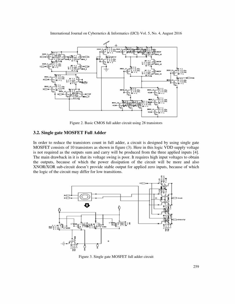
Starting with basic CMOS full adder circuit, it consists of 28 transistors as shown in figure 2,[3]
with less delay and high speed it also has good voltage swing, so the circuit’s performance will
be good but its power dissipation is more because the transistor’s count is high so the area
occupancy of the circuit is more. This CMOS logic is the basic logic operation of any circuit. It
has PMOS in the pull up mode and NMOS in the pull down mode, so reducing the transistors
count in the logic circuit is very difficult.
International Journal on Cybernetics & Informatics (IJCI) Vol. 5, No. 4, August 2016
259
Figure 2. Basic CMOS full adder circuit using 28 transistors
3.2. Single gate MOSFET Full Adder
In order to reduce the transistors count in full adder, a circuit is designed by using single gate
MOSFET consists of 10 transistors as shown in figure (3). Here in this logic VDD supply voltage
is not required as the outputs sum and carry will be produced from the three applied inputs [4].
The main drawback in it is that its voltage swing is poor. It requires high input voltages to obtain
the outputs, because of which the power dissipation of the circuit will be more and also
XNOR/XOR sub-circuit doesn’t provide stable output for applied zero inputs, because of which
the logic of the circuit may differ for low transitions.
Figure 3. Single gate MOSFET full adder circuit

International Journal on Cybernetics & Informatics (IJCI) Vol. 5, No. 4, August 2016
260
3.3. Double gate MOSFET Full Adder
To overcome the drawbacks in Single gate MOSFET i.e., to increase the output voltage swing in
Single gate MOSFET a double gate MOSFET is designed by connecting two single gate
transistors back to back in such a way that sources and drains of two single gate MOSFET
transistors are connected respectively as shown in figure (4).This circuit has 4 pairs of NMOS
and 6 pairs of PMOS. The logic and analysis is similar to Single gate MOSFET except voltage
swing. But the draw back in this case is that it consumes more power when compared to single
gate MOSFET. Generally size of PMOS is doubled than size of NMOS but in Double gate
MOSFET W/L ratio is maintained as 1:1 for all transistors, because of which there is leakage in
PMOS transistors [4]. The W/L ratio is maintained so as to attain sufficient output voltage swing.
Figure 4. Double gate MOSFET full adder circuit
4. PROPOSED FULL ADDER CIRCUITS USING 22nm TECHNOLOGY
4.1. Transmission Gate full adder
A transmission gate has three inputs, called source, n-gate, and p-gate; and it has one output,
called drain. The values at n-gate and p-gate are expected to be opposite to each other. If p-
gate is 0 while n-gate is 1, then the value found at source is transmitted to drain. If p-gate is 1
while p-gate is 0, then the connection is broken, so the value at drain is left floating. In all other
cases, drain receives an error output — unless source is floating, in which case drain is floating
as well. as shown in figure (5). In this logic, one PMOS transistor and one NMOS transistor is
connected back to back. This circuit has 4 pairs of Transmission Gates as shown in figure (5)[5].
The Transmission gates are used to increase the output voltage level of MOSFET’s which drives
their output as input to a particular MOSFET for increase in output voltage swing. It overcomes
the drawbacks in pass transistor logic and above mentioned logics in section II. As transistor
count is reduced without effect in performance, this circuit is preferred. It can be operated at
different loads and at different frequency of operations

International Journal on Cybernetics & Informatics (IJCI) Vol. 5, No. 4, August 2016
261
Table 1: Transmission gate full adder logic
p-gate n-gate drain
0 0 X*
0 1 source
1 0 Z
1 1 X*
X/Z any X*
Any X/Z X*
* If source is Z, drain is Z; otherwise drain is X.
Figure 5. Transmission Gate full adder circuit
4.2. GDI
The architecture of the 2:1 MUX using GDI method is shown in fig 6.[6] In this we have
connected NMOS and PMOS gate along with a SEL line ‘A’, as in MUX. As we know that
PMOS works on LOW and NMOS works on HIGH. So, when the SEL input is low, then the
PMOS get activated, and show the input ‘B’ in the output and due to low input the NMOS idle, as
it is activated in high input. For the same case, while the G input is high then the NMOS get
activated, and show the input ‘C’ at the output. Thus this circuitry behaves as a 2-input MUX
using ‘A’ as SEL line, and shows the favourable output as 2:1MUX. Now it's implemented the
low power full adder circuit with the help of 2T MUX, done by GDI technique. It require total 6
numbers of 2T MUX having same characteristics to design a 12T full adder [7].
4.2.1. Gate Diffusion Input Technique:
GDI technique offers realization of extensive variety of logic functions using simple two
transistor based circuit. This scheme gives for fast and low power circuit designs, which is reduce

International Journal on Cybernetics & Informatics (IJCI) Vol. 5, No. 4, August 2016
262
the number of MOS transistors as compared to CMOS design and also other existing low power
techniques, while the logic level swing and static power dissipation improves.
GDI technique based full adders have advantages over the full adder using pass transistor and is
categorized by tremendous speed and low power. This technique has been described below:
1. The GDI cell consists of one nMOS and one pMOS. The structure looks CMOS inverter.
Though in case of GDI both the sources and corresponding substrate terminals are not connected
with supply and it can be randomly biased.
2. It has three input terminals: G (nMOS and pMOS gate input shorted), P (pMOS source input),
and N (nMOS source input). The output is taken from D (nMOS and pMOS drain terminal
shorted).
The digital circuit can be analyzed logically with the help of simple Boolean algebra. The output
of each MUX can be analyzed to get sum & carry.
Figure 6. GDI Full Adder
4.2.2. Logic Analysis:
The digital circuit shown in figure (6), can be analyzed logically with the help of simple Boolean
algebra [8]. The outputs of each MUX can be analyzed to get the sum and carry.
MUX 1= (BA1+CA)
MUX 2 = (CA1+BA)
MUX 3= [(CA1+BA)C
1+(BA
1+CA)C]
= ABC1+A
1BC+AC
= ABC1+A
1BC+AC(B+B
1)
= ABC1+A
1BC+ABC+AB
1C
= ABC1+ABC+A
1BC+ ABC+ AB
1C+ABC
= AB(C+C1)+BC(A+A
1)+AC(B+B
1)
= AB+BC+AC=Cout
MUX 4=A1B+(A
1B+AC)B
MUX 5=(CA1+BA)B
1+AB
International Journal on Cybernetics & Informatics (IJCI) Vol. 5, No. 4, August 2016
263
MUX 6= [A1B+(A
1B+AC)B]C
1+[(CA
1+BA)B
1+AB]C
= AB1C
1+A
1BC
1+ABC=SUM
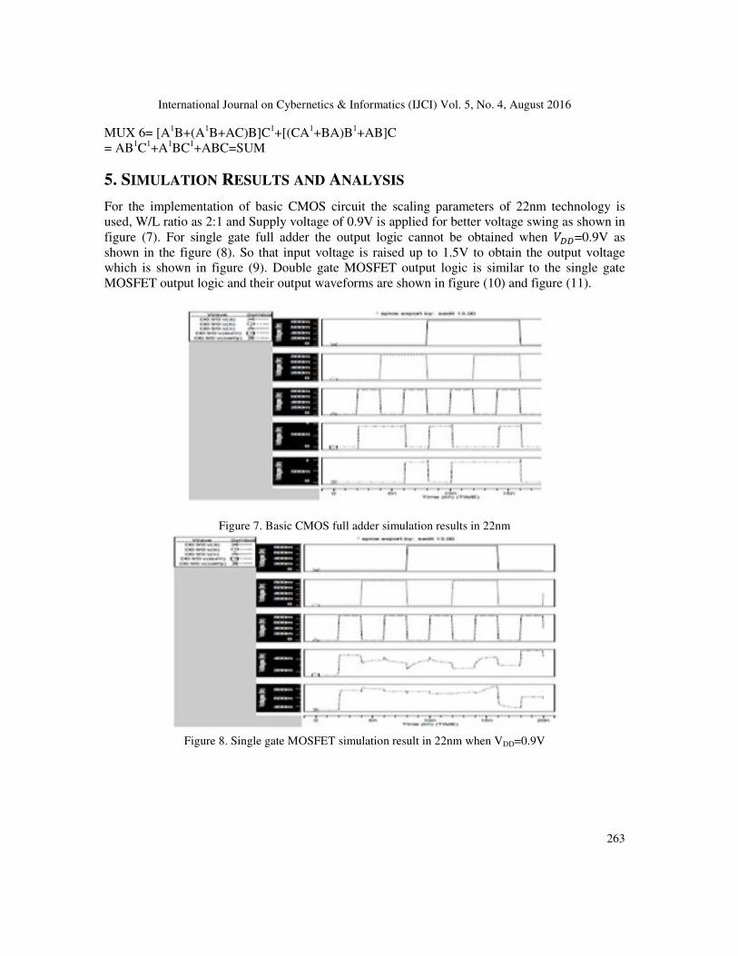
5. SIMULATION RESULTS AND ANALYSIS
For the implementation of basic CMOS circuit the scaling parameters of 22nm technology is
used, W/L ratio as 2:1 and Supply voltage of 0.9V is applied for better voltage swing as shown in
figure (7). For single gate full adder the output logic cannot be obtained when ���=0.9V as
shown in the figure (8). So that input voltage is raised up to 1.5V to obtain the output voltage
which is shown in figure (9). Double gate MOSFET output logic is similar to the single gate
MOSFET output logic and their output waveforms are shown in figure (10) and figure (11).
Figure 7. Basic CMOS full adder simulation results in 22nm
Figure 8. Single gate MOSFET simulation result in 22nm when VDD=0.9V

International Journal on Cybernetics & Informatics (IJCI) Vol. 5, No. 4, August 2016
264
Figure 9. Single gate MOSFET simulation results in 22nm when VDD=1.5V
Figure 10. Double gate MOSFET simulation result in 22nm when VDD=0.9V
Figure 11. Double gate MOSFET simulation results in 22nm when VDD=1.5V
International Journal on Cybernetics & Informatics (IJCI) Vol. 5, No. 4, August 2016
265
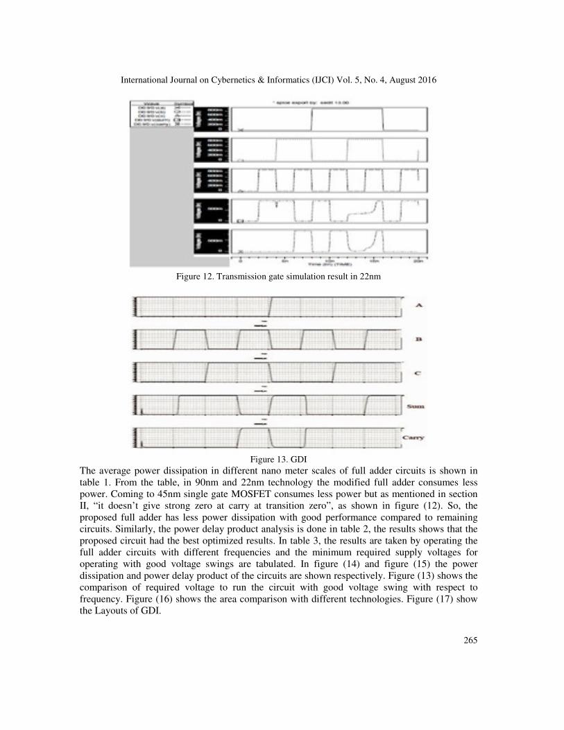
Figure 12. Transmission gate simulation result in 22nm
Figure 13. GDI
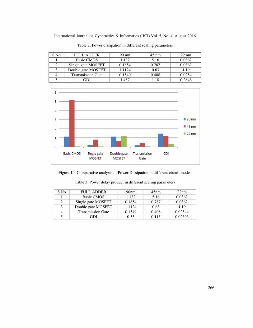
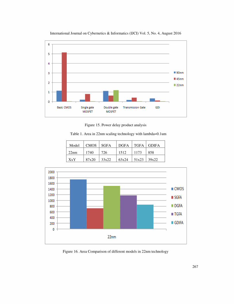
The average power dissipation in different nano meter scales of full adder circuits is shown in
table 1. From the table, in 90nm and 22nm technology the modified full adder consumes less
power. Coming to 45nm single gate MOSFET consumes less power but as mentioned in section
II, “it doesn’t give strong zero at carry at transition zero”, as shown in figure (12). So, the
proposed full adder has less power dissipation with good performance compared to remaining
circuits. Similarly, the power delay product analysis is done in table 2, the results shows that the
proposed circuit had the best optimized results. In table 3, the results are taken by operating the
full adder circuits with different frequencies and the minimum required supply voltages for
operating with good voltage swings are tabulated. In figure (14) and figure (15) the power
dissipation and power delay product of the circuits are shown respectively. Figure (13) shows the
comparison of required voltage to run the circuit with good voltage swing with respect to
frequency. Figure (16) shows the area comparison with different technologies. Figure (17) show
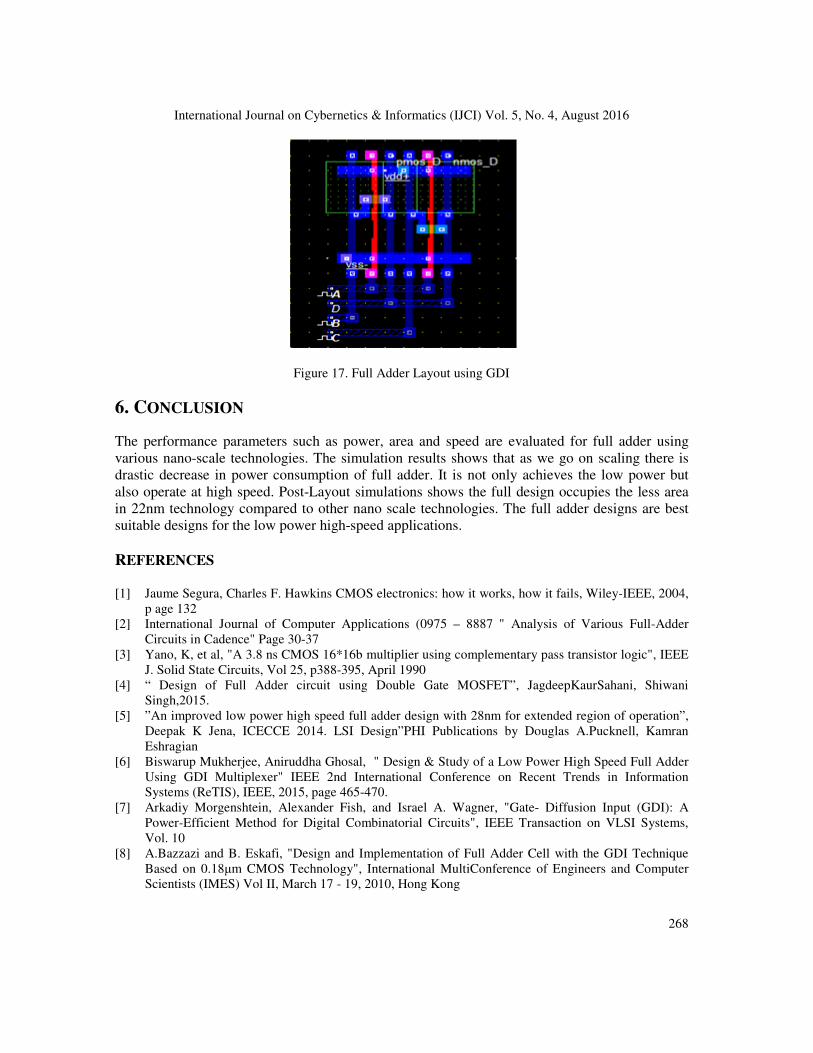
the Layouts of GDI.
International Journal on Cybernetics & Informatics (IJCI) Vol. 5, No. 4, August 2016
266
Table 2: Power dissipation in different scaling parameters
S.No FULL ADDER 90 nm 45 nm 22 nm
1 Basic CMOS 1.132 5.16 0.0362
2 Single gate MOSFET 0.1854 0.787 0.0362
3 Double gate MOSFET 1.1124 0.63 1.19
4 Transmission Gate 0.1549 0.408 0.0254
5 GDI 1.457 1.18 0.2846
Figure 14. Comparative analysis of Power Dissipation in different circuit modes
Table 3: Power delay product in different scaling parameters
S.No FULL ADDER 90nm 45nm 22nm
1 Basic CMOS 1.132 5.16 0.0362
2 Single gate MOSFET 0.1854 0.787 0.0362
3 Double gate MOSFET 1.1124 0.63 1.19
4 Transmission Gate 0.1549 0.408 0.02544
5 GDI 0.33 0.115 0.02393
International Journal on Cybernetics & Informatics (IJCI) Vol. 5, No. 4, August 2016
267
Figure 15. Power delay product analysis
Table 1. Area in 22nm scaling technology with lambda=0.1um
Model CMOS SGFA DGFA TGFA GDIFA
22nm 1740 726 1512 1173 858
XxY 87x20 33x22 63x24 51x23 39x22
Figure 16. Area Comparison of different models in 22nm technology
International Journal on Cybernetics & Informatics (IJCI) Vol. 5, No. 4, August 2016
268
Figure 17. Full Adder Layout using GDI
6. CONCLUSION
The performance parameters such as power, area and speed are evaluated for full adder using
various nano-scale technologies. The simulation results shows that as we go on scaling there is
drastic decrease in power consumption of full adder. It is not only achieves the low power but
also operate at high speed. Post-Layout simulations shows the full design occupies the less area
in 22nm technology compared to other nano scale technologies. The full adder designs are best
suitable designs for the low power high-speed applications.
REFERENCES [1] Jaume Segura, Charles F. Hawkins CMOS electronics: how it works, how it fails, Wiley-IEEE, 2004,
p age 132
[2] International Journal of Computer Applications (0975 – 8887 " Analysis of Various Full-Adder
Circuits in Cadence" Page 30-37
[3] Yano, K, et al, "A 3.8 ns CMOS 16*16b multiplier using complementary pass transistor logic", IEEE
J. Solid State Circuits, Vol 25, p388-395, April 1990
[4] “ Design of Full Adder circuit using Double Gate MOSFET”, JagdeepKaurSahani, Shiwani
Singh,2015.
[5] ”An improved low power high speed full adder design with 28nm for extended region of operation”,
Deepak K Jena, ICECCE 2014. LSI Design”PHI Publications by Douglas A.Pucknell, Kamran
Eshragian
[6] Biswarup Mukherjee, Aniruddha Ghosal, " Design & Study of a Low Power High Speed Full Adder
Using GDI Multiplexer" IEEE 2nd International Conference on Recent Trends in Information
Systems (ReTIS), IEEE, 2015, page 465-470.
[7] Arkadiy Morgenshtein, Alexander Fish, and Israel A. Wagner, "Gate- Diffusion Input (GDI): A
Power-Efficient Method for Digital Combinatorial Circuits", IEEE Transaction on VLSI Systems,
Vol. 10
[8] A.Bazzazi and B. Eskafi, "Design and Implementation of Full Adder Cell with the GDI Technique
Based on 0.18µm CMOS Technology", International MultiConference of Engineers and Computer
Scientists (IMES) Vol II, March 17 - 19, 2010, Hong Kong

International Journal on Cybernetics & Informatics (IJCI) Vol. 5, No. 4, August 2016
269
AUTHORS
Murali. A is a research scholar (Ph.D) from KL University and currently working as an
Associate Professor, Department of ECE at Raghu Engineering College,
Visakhapatnam, India. He has completed his M.Tech from IIT Madras Chennai. He has
10 years of experience including academic and Industry. He has published 9
International Journals and 8 National & International Conferences. His research
interests in Low Power VLSI Design, FPGA, Digital Circuits, Memory Design and
Embedded Systems.
Y.L.V Santhosh Kumar is currently working as an Assistant Professor, Department of
ECE at Raghu Engineering College, Visakhapatnam, India. He has completed his
M.Tech from PYDAH College of Engineering and Technology, Visakhapatnam. He has
3 years of experience and Published 5 papers in International Journals. His research
interests in Low Power VLSI Design, Digital Circuits and Signal Processer.
P. Rajesh received his B.Tech degree from Raghu Engineering College in the year
2011 and received M.Tech degree from MVGR College of Engineering in the year
2013. He is working as an Assistant Professor in the Department of Electronics and
Communication Engineering at Raghu Engineering College. He has published three
Papers in International Journals. His research activities are related to Low power VLSI
Design.
Related Documents