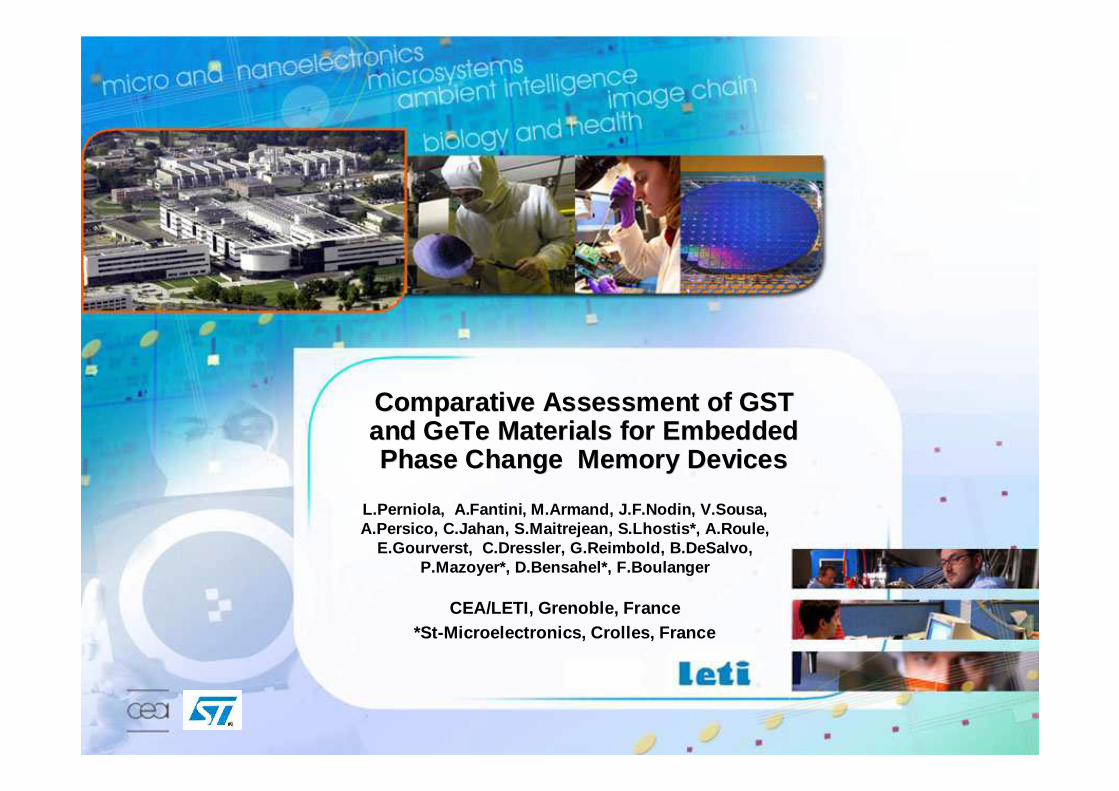
1 2007 © CEA 2009. All rights reserved Any reproduction in whole or in part on any medium or use of the information contained herein is prohibited without the prior written consent of CEA Comparative Assessment of GST Comparative Assessment of GST and and GeTe GeTe Materials for Embedded Materials for Embedded Phase Change Memory Devices Phase Change Memory Devices L.Perniola, A.Fantini, M.Armand, J.F.Nodin, V.Sousa, A.Persico, C.Jahan, S.Maitrejean, S.Lhostis*, A.Roule, E.Gourverst, C.Dressler, G.Reimbold, B.DeSalvo, P.Mazoyer*, D.Bensahel*, F.Boulanger CEA/LETI, Grenoble, France *St-Microelectronics, Crolles, France

Welcome message from author
This document is posted to help you gain knowledge. Please leave a comment to let me know what you think about it! Share it to your friends and learn new things together.
Transcript
1
2007
© CEA 2009. All rights reservedAny reproduction in whole or in part on any medium or use of the information contained herein
is prohibited without the prior written consent of CEA
Comparative Assessment of GST Comparative Assessment of GST and and GeTeGeTe Materials for Embedded Materials for Embedded Phase Change Memory DevicesPhase Change Memory Devices
L.Perniola, A.Fantini, M.Armand, J.F.Nodin, V.Sous a, A.Persico, C.Jahan, S.Maitrejean, S.Lhostis*, A.Rou le,
E.Gourverst, C.Dressler, G.Reimbold, B.DeSalvo, P.Mazoyer*, D.Bensahel*, F.Boulanger
CEA/LETI, Grenoble, France*St-Microelectronics, Crolles, France
2
2007
© CEA 2009. All rights reservedAny reproduction in whole or in part on any medium or use of the information contained herein
is prohibited without the prior written consent of CEA
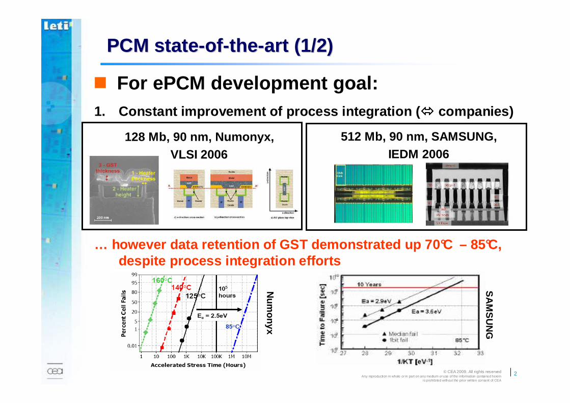
PCM statePCM state --ofof --thethe --art (1/2)art (1/2)
For ePCM development goal:
128 Mb, 90 nm, Numonyx, VLSI 2006
512 Mb, 90 nm, SAMSUNG, IEDM 2006
SA
MS
UN
G
Num
onyx
1. Constant improvement of process integration ( companies)
… however data retention of GST demonstrated up 70°C – 85°C, despite process integration efforts
3
2007
© CEA 2009. All rights reservedAny reproduction in whole or in part on any medium or use of the information contained herein
is prohibited without the prior written consent of CEA
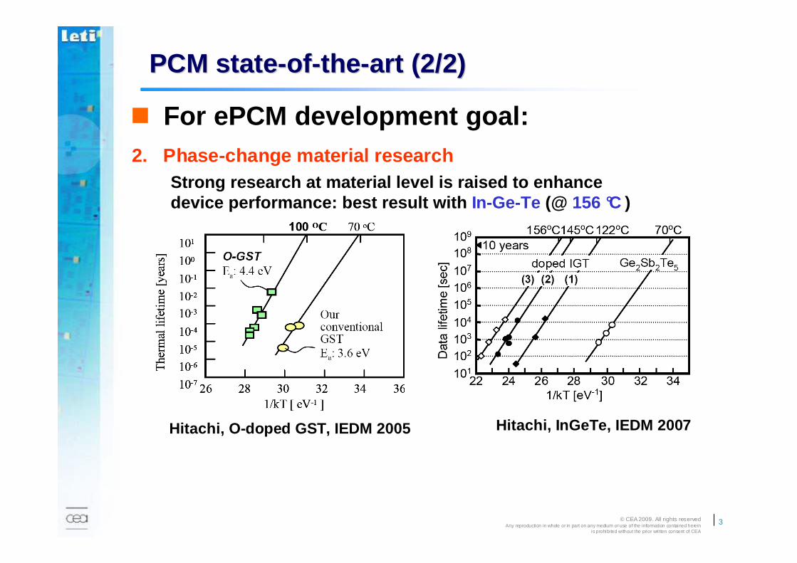
For ePCM development goal:2. Phase-change material research
Strong research at material level is raised to enha nce device performance: best result with In-Ge-Te (@ 156 °C )
Hitachi, O-doped GST, IEDM 2005 Hitachi, InGeTe, IEDM 2007
PCM statePCM state --ofof --thethe --art (2/2)art (2/2)
4
2007
© CEA 2009. All rights reservedAny reproduction in whole or in part on any medium or use of the information contained herein
is prohibited without the prior written consent of CEA
OutlineOutline
Introduction
Approach
Material Study
Electrical Characterization
Summary
5
2007
© CEA 2009. All rights reservedAny reproduction in whole or in part on any medium or use of the information contained herein
is prohibited without the prior written consent of CEA
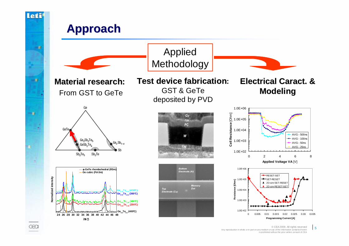
AppliedMethodology
CT200
24 26 28 30 32 34 36 38 40 42 44 46 48
Ge0.62Te0.38 (400°C)
Ge cubic (Fd-3m)αααα-GeTe rhombohedral (R3m)
Nor
ma
lized
inte
nsity
Ge0.76Te0.24 (400°C)Ge
0.76Te
0.24 (360°C)
Ge0.62
Te0.38
(250°C)
Ge0.5
Te0.5
(400°C)
2θθθθ (°)
Material research:Material research:From GST to GeTe
ApproachApproach
Test Test devicedevice fabricationfabrication :GST & GeTe
deposited by PVD
Electrical Electrical CaractCaract . & . & ModelingModeling
1.0E+02
1.0E+03
1.0E+04
1.0E+05
1.0E+06
0 0.005 0.01 0.015 0.02 0.025 0.03 0.035
Programming Current [A]
Re
sist
anc
e [O
hm]
RESET-SET
SET-RESET
2D sim SET-RESET
2D sim RESET-SET
1.0E+02
1.0E+03
1.0E+04
1.0E+05
1.0E+06
0 2 4 6 8
Applied Voltage VA [V]
Cel
l Res
ista
nce
[Ohm
]
AVG - 500ns
AVG - 100ns
AVG - 50ns
AVG - 25ns
6
2007
© CEA 2009. All rights reservedAny reproduction in whole or in part on any medium or use of the information contained herein
is prohibited without the prior written consent of CEA
OutlineOutline
Introduction
Approach
Material Study
Electrical Characterization
Summary
7
2007
© CEA 2009. All rights reservedAny reproduction in whole or in part on any medium or use of the information contained herein
is prohibited without the prior written consent of CEA
CT200
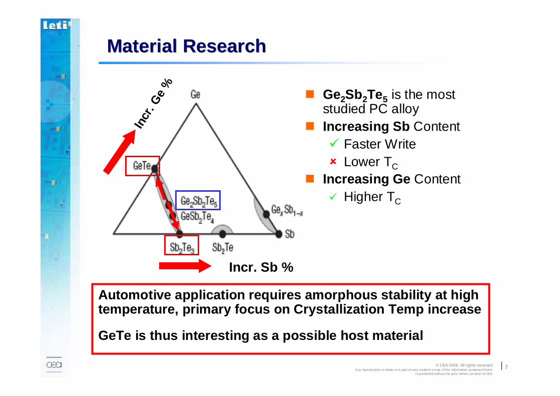
Material Material ResearchResearch
Incr
. Ge
%
Incr. Sb %
Automotive application requires amorphous stability at high temperature, primary focus on Crystallization Temp increase
GeTe is thus interesting as a possible host material
Ge2Sb2Te5 is the most studied PC alloy
Increasing Sb Content Faster Write Lower TC
Increasing Ge Content Higher TC
8
2007
© CEA 2009. All rights reservedAny reproduction in whole or in part on any medium or use of the information contained herein
is prohibited without the prior written consent of CEA
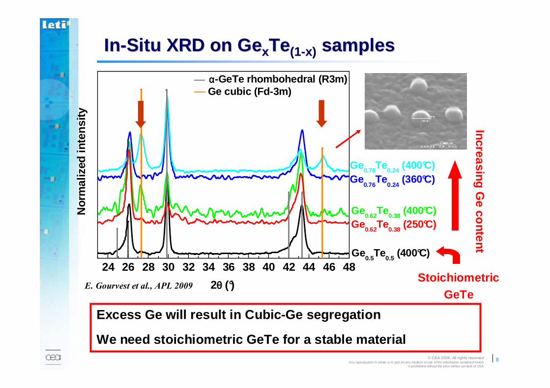
InIn--Situ XRD on GeSitu XRD on Ge xxTeTe(1(1--x)x) samplessamples
24 26 28 30 32 34 36 38 40 42 44 46 48
Ge0.62
Te0.38
(400°C)
Ge cubic (Fd-3m)αααα-GeTe rhombohedral (R3m)
Nor
mal
ized
inte
nsity
Ge0.76
Te0.24
(400°C)Ge
0.76Te
0.24 (360°C)
Ge0.62
Te0.38
(250°C)
Ge0.5
Te0.5
(400°C)
2θθθθ (°)Stoichiometric
GeTe
IncreasingG
e content
Excess Ge will result in Cubic-Ge segregation
We need stoichiometric GeTe for a stable material
E. Gourvest et al., APL 2009
9
2007
© CEA 2009. All rights reservedAny reproduction in whole or in part on any medium or use of the information contained herein
is prohibited without the prior written consent of CEA
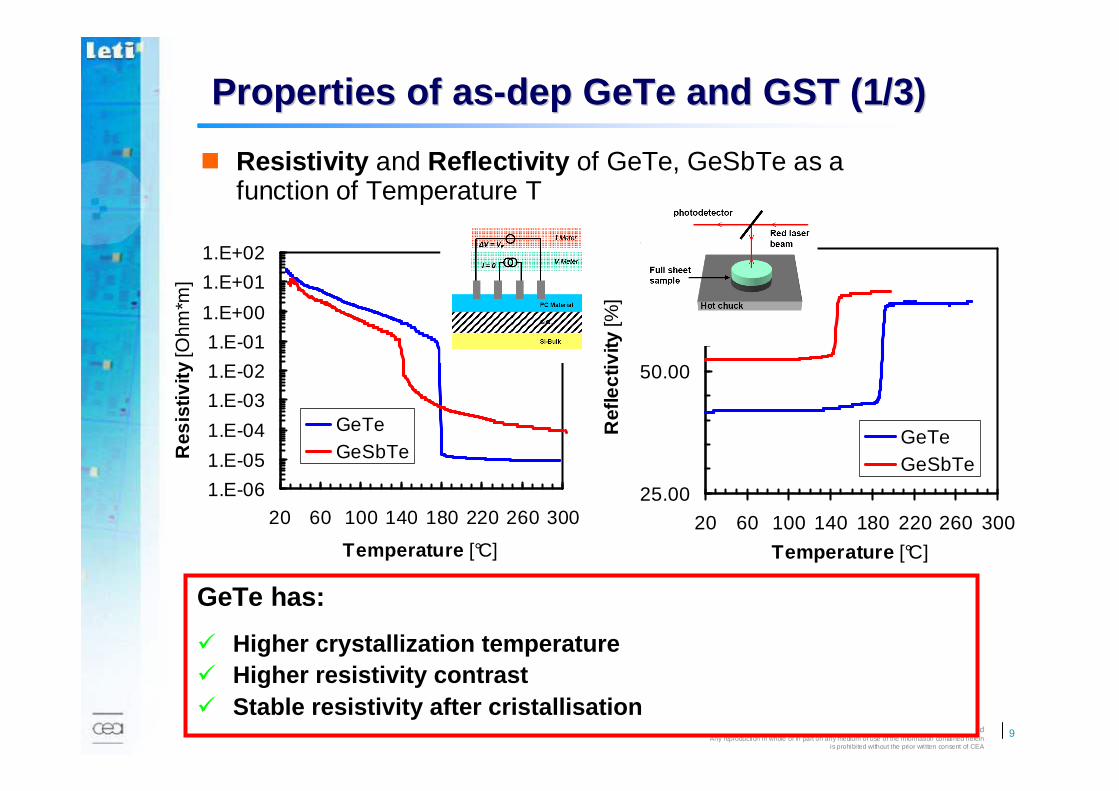
Properties of asProperties of as --depdep GeTeGeTe and GST (1/3)and GST (1/3)
Resistivity and Reflectivity of GeTe, GeSbTe as a function of Temperature T
GeTe has:
Higher crystallization temperature Higher resistivity contrast Stable resistivity after cristallisation
25.00
50.00
75.00
20 60 100 140 180 220 260 300
Temperature [°C]
Ref
lect
ivity
[%]
GeTeGeSbTe
1.E-06
1.E-05
1.E-04
1.E-03
1.E-02
1.E-01
1.E+00
1.E+01
1.E+02
20 60 100 140 180 220 260 300
Temperature [°C]
Res
istiv
ity
[Ohm
*m]
GeTeGeSbTe

10
2007
© CEA 2009. All rights reservedAny reproduction in whole or in part on any medium or use of the information contained herein
is prohibited without the prior written consent of CEA
Properties of asProperties of as --depdep GeTeGeTe and GST (2/3)and GST (2/3)
Resistivity of GeTe, GeSbTe as function of time
Different shapes:Probably stronger growth process in GeTe
1.0E+01
1.0E+02
1.0E+03
1.0E+04
1.0E+05
1.0E+06
1.0E+07
10 100 1000 10000Time [s]
Squ
are
Res
ista
nce
[Ohm
/sq]
GeTe 155 °C
GeTe 165 °C
GeTe 175 °C
GeTe
1.0E+01
1.0E+02
1.0E+03
1.0E+04
1.0E+05
1.0E+06
1.0E+07
10 100 1000 10000Time [s]
Sq
uare
Res
ista
nce
[Ohm
/sq]
GST 125 °C
GST 130 °C
GST 135 °C
GST 140 °C
GeSbTe
11
2007
© CEA 2009. All rights reservedAny reproduction in whole or in part on any medium or use of the information contained herein
is prohibited without the prior written consent of CEA
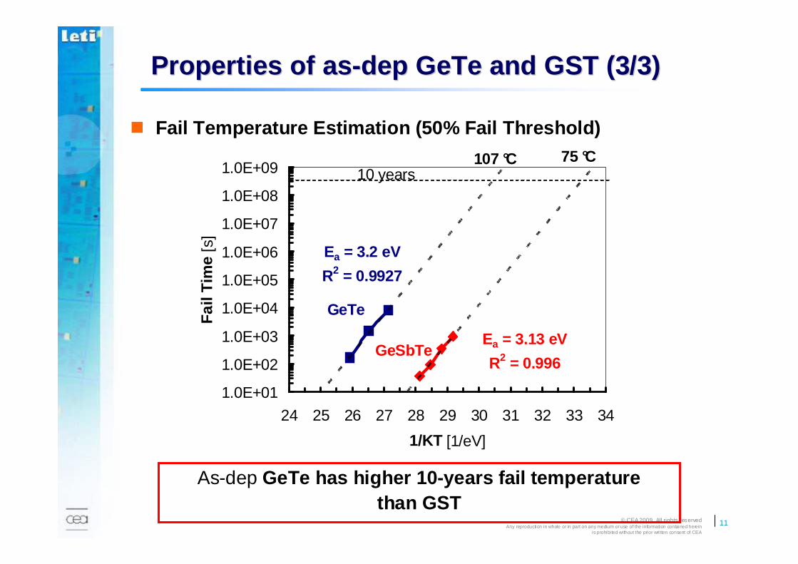
GST 50% fail
Ea = 3.13 eV
R2 = 0.996
Ea = 3.2 eV
R2 = 0.9927
1.0E+01
1.0E+02
1.0E+03
1.0E+04
1.0E+05
1.0E+06
1.0E+07
1.0E+08
1.0E+09
24 25 26 27 28 29 30 31 32 33 34
1/KT [1/eV]
Fai
l Tim
e [s
]
75 °C107 °C
GeTe
GeSbTe
10 years
As-dep GeTe has higher 10-years fail temperature than GST
Properties of asProperties of as --depdep GeTeGeTe and GST (3/3)and GST (3/3)
Fail Temperature Estimation (50% Fail Threshold)
12
2007
© CEA 2009. All rights reservedAny reproduction in whole or in part on any medium or use of the information contained herein
is prohibited without the prior written consent of CEA
OutlineOutline
Introduction
Approach
Material Study
Electrical Characterization
Summary
13
2007
© CEA 2009. All rights reservedAny reproduction in whole or in part on any medium or use of the information contained herein
is prohibited without the prior written consent of CEA
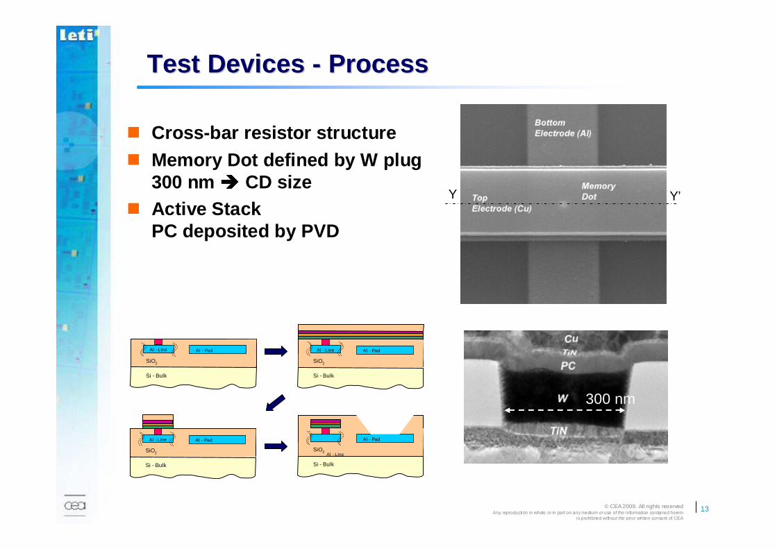
Y Y’
Test Devices Test Devices -- ProcessProcess
Al - Line Al - Pad
SiO2
Si - Bulk
Al - Line Al - Pad
SiO2
Si - Bulk
Al - Line Al - Pad
SiO2
Si - Bulk
Al - Line
Al - Pad
SiO2
Si - Bulk
300 nm
Cross-bar resistor structure Memory Dot defined by W plug
300 nm CD size Active Stack
PC deposited by PVD
14
2007
© CEA 2009. All rights reservedAny reproduction in whole or in part on any medium or use of the information contained herein
is prohibited without the prior written consent of CEA
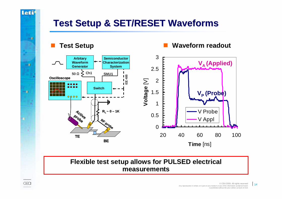
Test Setup & SET/RESET WaveformsTest Setup & SET/RESET Waveforms
Flexible test setup allows for PULSED electrical measurements
ArbitaryWaveformGenerator
SemiconductorCharacterization
System
S
G
Oscilloscope
Activeprobe RF probe
TEBE
Ch1 SMU1
IEE
48
8
Switch
RL ~ 0 – 1K
50 Ω
ArbitaryWaveformGenerator
SemiconductorCharacterization
System
S
G
Oscilloscope
Activeprobe RF probe
TEBE
Ch1 SMU1
IEE
48
8
Switch
RL ~ 0 – 1K
50 Ω
Test Setup
0
0.5
1
1.5
2
2.5
3
20 40 60 80 100
Time [ns]V
olta
ge [
V]
V ProbeV Appl
VA (Applied)
VP (Probe)
Waveform readout
15
2007
© CEA 2009. All rights reservedAny reproduction in whole or in part on any medium or use of the information contained herein
is prohibited without the prior written consent of CEA
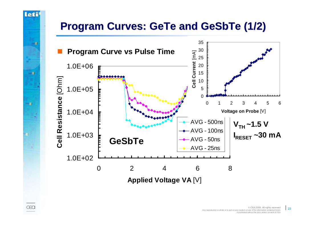
Program Curves: Program Curves: GeTeGeTe and and GeSbTeGeSbTe (1/2)(1/2)
1.0E+02
1.0E+03
1.0E+04
1.0E+05
1.0E+06
0 2 4 6 8
Applied Voltage VA [V]
Cel
l Res
ista
nce
[Ohm
]
AVG - 500ns
AVG - 100ns
AVG - 50ns
AVG - 25nsGeSbTe
Program Curve vs Pulse Time
0
5
10
15
20
25
30
35
0 1 2 3 4 5 6
Voltage on Probe [V]
Ce
ll C
urre
nt [m
A]
VTH ~1.5 VIRESET ~30 mA

16
2007
© CEA 2009. All rights reservedAny reproduction in whole or in part on any medium or use of the information contained herein
is prohibited without the prior written consent of CEA
Data Retention: Data Retention: GeTeGeTe DevicesDevices
GeTe: Longer fail times at HT compared to GST
Room for improvement will probably come from optimi zed RESET procedure and optimized test device structure s
0.10
1.00
10.00
10 100 1000 10000 100000Time [s]
Nor
mal
ized
Res
ista
nce GeTe 120 °C
GeTe 175 °C
GeSbTe 120 °C
17
2007
© CEA 2009. All rights reservedAny reproduction in whole or in part on any medium or use of the information contained herein
is prohibited without the prior written consent of CEA
OutlineOutline
Introduction
Approach
Material Study
Electrical Characterization
Summary
18
2007
© CEA 2009. All rights reservedAny reproduction in whole or in part on any medium or use of the information contained herein
is prohibited without the prior written consent of CEA
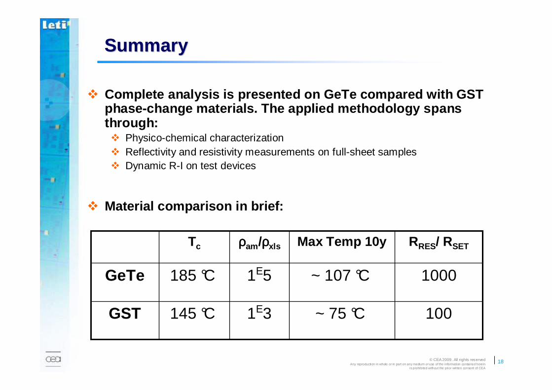
SummarySummary
Complete analysis is presented on GeTe compared with GST phase-change materials. The applied methodology spa ns through: Physico-chemical characterization Reflectivity and resistivity measurements on full-sheet samples Dynamic R-I on test devices
100~ 75 °C1E3145 °CGST
1000~ 107 °C1E5185 °CGeTe
RRES/ RSETMax Temp 10yρρρρam/ρρρρxlsTc
Material comparison in brief:

19
2007
© CEA 2009. All rights reservedAny reproduction in whole or in part on any medium or use of the information contained herein
is prohibited without the prior written consent of CEA
THANK YOU FOR THANK YOU FOR YOUR ATTENTIONYOUR ATTENTION
20
2007
© CEA 2009. All rights reservedAny reproduction in whole or in part on any medium or use of the information contained herein
is prohibited without the prior written consent of CEA
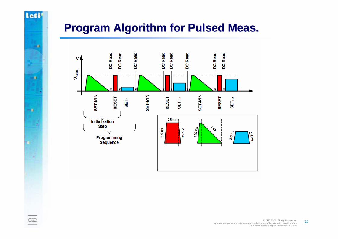
Program Algorithm for Pulsed Meas.Program Algorithm for Pulsed Meas.
Related Documents