Contents lists available at ScienceDirect Cryogenics journal homepage: www.elsevier.com/locate/cryogenics Research paper Compact Si JFET model for cryogenic temperature Konstantin O. Petrosyants a,b, ⁎ , Mamed R. Ismail-zade a , Lev M. Sambursky a,b a National Research University Higher School of Economics (Moscow Institute of Electronics and Mathematics), Moscow, Russian Federation b Institute for Design Problems in Microelectronics, Russian Academy of Sciences, Zelenograd, Moscow, Russian Federation ARTICLEINFO Keywords: JFET transistors Cryogenic temperature Low-temperature effects Compact transistor models Model parameter extraction experimental I-V- characteristics Spice-like circuit simulators ABSTRACT Compact Si JFET model for SPICE circuit simulation in the extended temperature range from 373 K down to 73 K (+100 °C…−200 °C) is proposed. It is based on the standard JFET model Level = 3 (Statz model) with the full set of temperature-dependent parameters in the cryogenic temperature range. The universal procedure for model parameter extraction from I-V-characteristic measurement data at low temperature is developed. The simulation error does not exceed 10–15% in the temperature range 373 K…73 K. The JFET Low-T model is implemented in the form of a subcircuit and tested in popular SPICE-like circuit simulators: HSPICE, LTSpice, ADS, and OrCAD. 1. Introduction Junction Field Effect Transistors (JFETs) due to high input re- sistance and amplification factor, low intrinsic noise and compatibility with Bi-CMOS/Bi-CMOS-DMOS technologies are widely used in input and subsequent cascades of low-noise operational amplifiers, com- parators, secondary power sources, stabilizers and other analog circuits of low-temperature electronics [1,2]. In Fig. 1a and b the typical structures of the integrated [3] and discrete [4] JFET transistors are shown. Different versions of compact models of JFETs were developed previously and built into the SPICE-like software tools for electronic circuits simulation [5–11]. These models guarantee the satisfactory accuracy only in the standard temperature range from 213 K to 423 K (−60 °C to +150 °C). In fact, there are no publications on the simulation of static I-V characteristics in the low temperature range. Few attempts were made to use the conventional JFET models for the qualitative analysis of analog circuits characteristics in the low-signal mode [12–14]. In our previous work [15] we tried to use the improved version of Shich- man–Hodges model for analog circuit simulation in cryogenic tem- perature range, but the possibilities of this model were limited. Unfortunately, no models are applicable to IC simulation at the cryogenic temperatures. Therefore, the goals of this work are: (1) To overcome the limitations of the conventional JFET models and develop the adequate compact Si JFET model with extended tem- perature range from 373 K down to 73 K; (2) To include the developed Low-T JFET model into commercial ver- sions of SPICE-like software tools to expand them to electronic circuit simulation for cryogenic applications. 2. Model formulation The most advanced in practical IC simulation is the standard JFET model Level 3 (Statz model [8]) implemented in popular SPICE-like simulators HSPICE, LTSpice, Eldo and others. It was employed as a core for the Low-T model version development. It assumes the common smooth I-V equation that describes JFET static I-V characteristics in three regions of operation: pinch-off, saturation and linear: = + × × ( ) I Beta V VTO Gamma V Lambda V Alpha ·( · ) ·(1 · ) 1 1 · , DS GS DS VGEXP DS V 3 3 DS (1) where I DS is the drain to source current; V DS , V GS are drain-source and gate-source voltage; Beta is the transconductance coefficient; Gamma is V DS multiplication factor; Lambda is the channel length modulation coefficient; Alpha is the saturation factor; VTO is the threshold voltage; VGEXP is the gate voltage exponent. The limitations of this model in the low-temperature range are il- lustrated by the example of I-V characteristics simulation for the 1.2 µm p-JFET as a part of the analog matrix array [3]. It is seen in Fig. 2a that in the conventional temperature range 373 K…193 K the satisfactory https://doi.org/10.1016/j.cryogenics.2020.103069 Received 18 March 2019; Received in revised form 5 February 2020; Accepted 16 March 2020 ⁎ Corresponding author at: National Research University Higher School of Economics (Moscow Institute of Electronics and Mathematics), Moscow, Russian Federation. E-mail address: [email protected] (K.O. Petrosyants). Cryogenics 108 (2020) 103069 Available online 23 March 2020 0011-2275/ © 2020 Elsevier Ltd. All rights reserved. T

Welcome message from author
This document is posted to help you gain knowledge. Please leave a comment to let me know what you think about it! Share it to your friends and learn new things together.
Transcript
Contents lists available at ScienceDirect
Cryogenics
journal homepage: www.elsevier.com/locate/cryogenics
Research paper
Compact Si JFET model for cryogenic temperatureKonstantin O. Petrosyantsa,b,⁎, Mamed R. Ismail-zadea, Lev M. Samburskya,baNational Research University Higher School of Economics (Moscow Institute of Electronics and Mathematics), Moscow, Russian Federationb Institute for Design Problems in Microelectronics, Russian Academy of Sciences, Zelenograd, Moscow, Russian Federation
A R T I C L E I N F O
Keywords:JFET transistorsCryogenic temperatureLow-temperature effectsCompact transistor modelsModel parameter extractionexperimental I-V- characteristicsSpice-like circuit simulators
A B S T R A C T
Compact Si JFET model for SPICE circuit simulation in the extended temperature range from 373 K down to 73 K(+100 °C…−200 °C) is proposed. It is based on the standard JFET model Level = 3 (Statz model) with the fullset of temperature-dependent parameters in the cryogenic temperature range. The universal procedure for modelparameter extraction from I-V-characteristic measurement data at low temperature is developed. The simulationerror does not exceed 10–15% in the temperature range 373 K…73 K. The JFET Low-T model is implemented inthe form of a subcircuit and tested in popular SPICE-like circuit simulators: HSPICE, LTSpice, ADS, and OrCAD.
1. Introduction
Junction Field Effect Transistors (JFETs) due to high input re-sistance and amplification factor, low intrinsic noise and compatibilitywith Bi-CMOS/Bi-CMOS-DMOS technologies are widely used in inputand subsequent cascades of low-noise operational amplifiers, com-parators, secondary power sources, stabilizers and other analog circuitsof low-temperature electronics [1,2]. In Fig. 1a and b the typicalstructures of the integrated [3] and discrete [4] JFET transistors areshown.
Different versions of compact models of JFETs were developedpreviously and built into the SPICE-like software tools for electroniccircuits simulation [5–11]. These models guarantee the satisfactoryaccuracy only in the standard temperature range from 213 K to 423 K(−60 °C to +150 °C).
In fact, there are no publications on the simulation of static I-Vcharacteristics in the low temperature range. Few attempts were madeto use the conventional JFET models for the qualitative analysis ofanalog circuits characteristics in the low-signal mode [12–14]. In ourprevious work [15] we tried to use the improved version of Shich-man–Hodges model for analog circuit simulation in cryogenic tem-perature range, but the possibilities of this model were limited.
Unfortunately, no models are applicable to IC simulation at thecryogenic temperatures.
Therefore, the goals of this work are:
(1) To overcome the limitations of the conventional JFET models and
develop the adequate compact Si JFET model with extended tem-perature range from 373 K down to 73 K;
(2) To include the developed Low-T JFET model into commercial ver-sions of SPICE-like software tools to expand them to electroniccircuit simulation for cryogenic applications.
2. Model formulation
The most advanced in practical IC simulation is the standard JFETmodel Level 3 (Statz model [8]) implemented in popular SPICE-likesimulators HSPICE, LTSpice, Eldo and others. It was employed as a corefor the Low-T model version development. It assumes the commonsmooth I-V equation that describes JFET static I-V characteristics inthree regions of operation: pinch-off, saturation and linear:
= + ×
× ( )I Beta V VTO Gamma V Lambda V
Alpha
·( · ) ·(1 · )
1 1 · ,
DS GS DSVGEXP
DS
V3
3DS(1)
where IDS is the drain to source current; VDS, VGS are drain-source andgate-source voltage; Beta is the transconductance coefficient; Gamma isVDS multiplication factor; Lambda is the channel length modulationcoefficient; Alpha is the saturation factor; VTO is the threshold voltage;VGEXP is the gate voltage exponent.
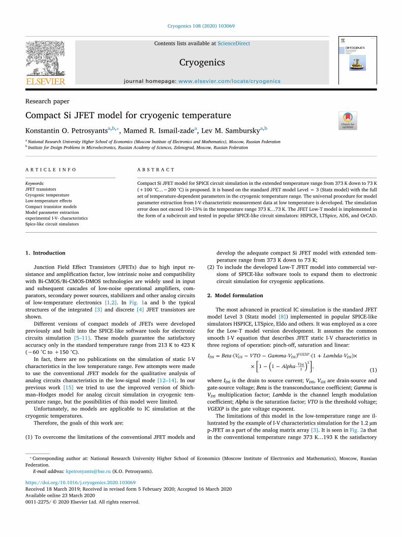
The limitations of this model in the low-temperature range are il-lustrated by the example of I-V characteristics simulation for the 1.2 µmp-JFET as a part of the analog matrix array [3]. It is seen in Fig. 2a thatin the conventional temperature range 373 K…193 K the satisfactory
https://doi.org/10.1016/j.cryogenics.2020.103069Received 18 March 2019; Received in revised form 5 February 2020; Accepted 16 March 2020
⁎ Corresponding author at: National Research University Higher School of Economics (Moscow Institute of Electronics and Mathematics), Moscow, RussianFederation.
E-mail address: [email protected] (K.O. Petrosyants).
Cryogenics 108 (2020) 103069
Available online 23 March 20200011-2275/ © 2020 Elsevier Ltd. All rights reserved.
T
accuracy of modeling is achieved, but in Fig. 2b for the low temperaturerange, when the temperature falls down from 160 K to 73 K, the si-mulation error increases rapidly, and the modeling results become to-tally unsatisfactory.
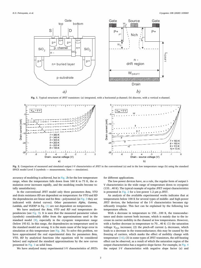
In the conventional JFET model only three parameters Beta, VTOand drain resistance RD are dependent on temperature: for VTO and RDthe dependencies are linear and for Beta – polynomial (in Fig. 3 they areindicated with dotted curves). Other parameters Alpha, Gamma,Lambda, and VGEXP in Eq. (1) are not dependent on temperature.
We have analyzed the Beta, VTO and RD real temperature de-pendencies (see Fig. 3). It is seen that the measured parameter values(symbols) considerably differ from the approximations used in thestandard model [8], especially in the cryogenic temperature range(below 193 K). In this range, the dependencies on temperature used inthe standard model are wrong. It is the main cause of the large error insimulation at this temperature (see Fig. 2b). To solve this problem, wehave approximated the real experimental data for parameters Beta,VTO, RD by analytical functions (the equations will be consideredbelow) and replaced the standard approximations by the new curvespresented in Fig. 3 as solid lines.
We have analyzed many experimental I-V characteristics of JFETs
for different applications.The low-power devices have, as a rule, the regular form of output I-
V characteristics in the wide range of temperature down to cryogenic(133…40 K). The typical example of regular JFET output characteristicsis presented in Fig. 2 for a low-power 1.2 μm p-JFET.
An analysis of the available experimental works indicates that attemperatures below 100 K for several types of middle- and high-powerJFET devices, the behaviour of the I-V characteristics becomes sig-nificantly irregular. This fact can be explained by the following lowtemperature effects.
With a decrease in temperature to 150…100 K, the transconduc-tance and drain current both increase, which is mainly due to the in-crease in carrier mobility in the channel at low temperatures. However,with a further decrease in temperature to 70…40 K: (1) the saturationvoltage VDsat increases; (2) the pinch-off current IP decreases, whichleads to a decrease in the transconductance; this may be caused by thefreezing of carriers, which masks the effect of mobility change withtemperature [16]; (3) in some types of JFET transistors, the self-heatingeffect can be observed, as a result of which the saturation region of theoutput characteristics has a negative slope factor. For example, in Fig. 4the output I-V characteristics with negative slope factor (a) and
Fig. 1. Typical structures of JFET transistors: (a) integrated, with a horizontal p-channel; (b) discrete, with a vertical n-channel.
Fig. 2. Comparison of measured and simulated output I-V characteristics of JFET in the conventional (a) and in the low temperature range (b) using the standardSPICE model Level 3 (symbols — measurements, lines — simulation).
K.O. Petrosyants, et al. Cryogenics 108 (2020) 103069
2
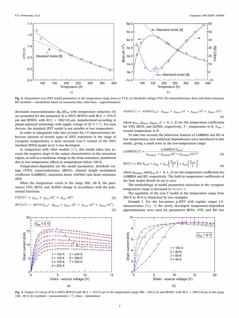
decreased transconductance dID/dVDS with temperature reduction (b)are presented for the symmetric Si n-JFETs BFW10 with W/L = 915/5μm and BFW61 with W/L = 340/3.8 μm, manufactured according toplanar-epitaxial technology with supply voltage of 25 V [17]. For suchdevices, the standard JFET model is not suitable at low temperature.
In order to adequately take into account the I-V characteristics be-haviour features of several types of JFET transistors in the range ofcryogenic temperatures, a more accurate Low-T version of the JFETstandard SPICE-model level 3 was developed.
In comparison with other models [15], this model takes into ac-count the negative slope of the output characteristics in the saturationregion, as well as a nonlinear change in the drain resistance, manifesteddue to low-temperature effects at temperatures below 100 K.
Temperature-dependent are the model parameters: threshold vol-tage (VTO), transconductance (BETA), channel length modulationcoefficient (LAMBDA), saturation factor (ALPHA) and drain resistance(RD).
When the temperature varies in the range 300…40 K, the para-meters VTO, BETA, and ALPHA change in accordance with the poly-nomial functions:
= + +VTO T p p T p T( ) · · ,vto vto vto0 1 22 (2)
= + + +BETA T BETA T p p T p T p T( ) ( ) · ( · · · ),nom beta beta beta beta0 1 22
33
(3)
= + + +ALPHA T ALPHA T p p T p T p T( ) ( ) · ( · · · ),nom alpha alpha alpha alpha0 1 22
33
(4)
where pvto,i, pbeta,i, palpha,i (i = 0, 1, 2) are the temperature coefficientsfor VTO, BETA, and ALPHA, respectively, T – temperature in K, Tnom –normal temperature in K.
To take into account the behaviour features of LAMBDA and RD atlow temperatures, new analytical dependencies were introduced in thismodel, giving a small error in the low-temperature range:
=+ +
LAMBDA T LAMBDA Tp p T p T
( ) ( )( )
,nom
lambda lambda lambda0 1 22 (5)
= + + +RD T RD T p p TT
p TT
( ) ( ) ,nom rd rdnom
rdnom
0 1 2
2
(6)
where plambda,i and prd,i (i= 0, 1, 2) are the temperature coefficients forLAMBDA and RD, respectively. The built-in temperature coefficients ofthe base model should be set to zero.
The methodology of model parameters extraction in the cryogenictemperature range is discussed in Section 4.
The capability of the Low-T model in the temperature range from300 K to 40 K is illustrated by two examples.
Example 1. For the low-power p-JFET with regular output I-V-characteristics (Fig. 2) the newly developed temperature-dependentapproximations were used for parameters BETA, VTO, and RD (see
Fig. 3. Dependence of p-JFET model parameters in the temperature range down to 73 K: (a) threshold voltage VTO; (b) transconductance Beta and drain resistanceRD (symbols – calculations based on measured data, solid lines – approximation).
Fig. 4. Output I-V curves of Si n-JFETs BFW10 with W/L = 915/5 µm in the temperature range 300…100 K (a) and BFW61 with W/L = 340/3.8 µm in the range100…40 K (b) (symbols – measurements [17], lines – simulation).
K.O. Petrosyants, et al. Cryogenics 108 (2020) 103069
3
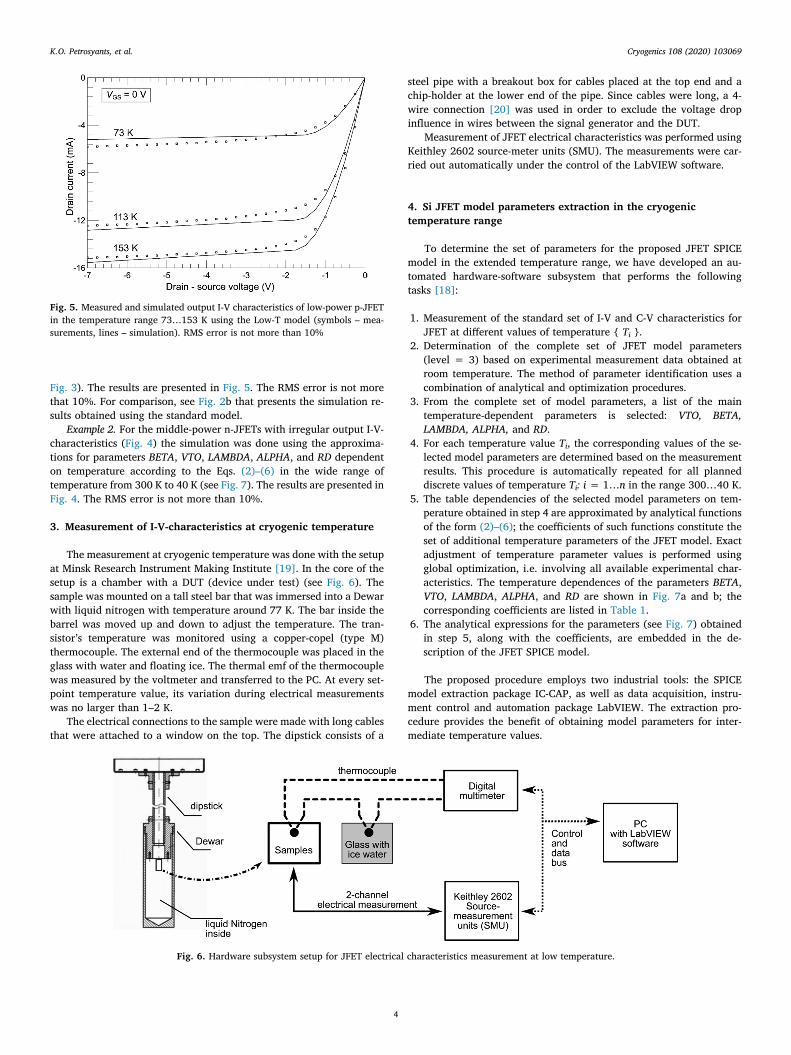
Fig. 3). The results are presented in Fig. 5. The RMS error is not morethat 10%. For comparison, see Fig. 2b that presents the simulation re-sults obtained using the standard model.
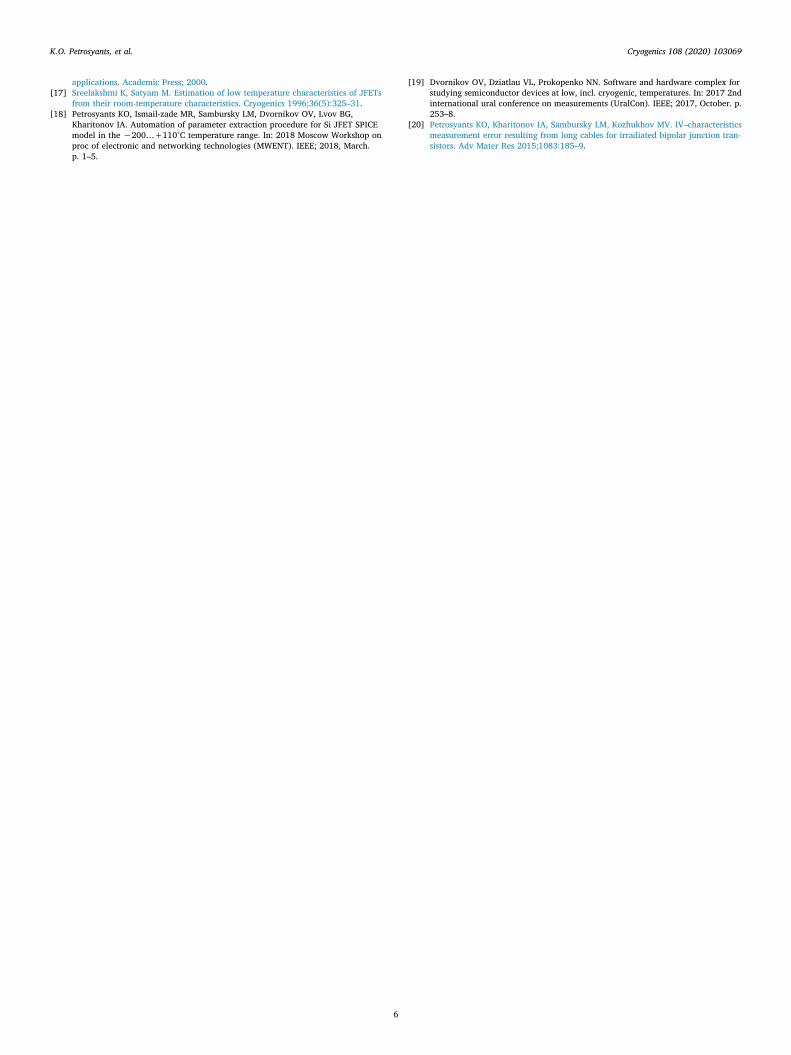
Example 2. For the middle-power n-JFETs with irregular output I-V-characteristics (Fig. 4) the simulation was done using the approxima-tions for parameters BETA, VTO, LAMBDA, ALPHA, and RD dependenton temperature according to the Eqs. (2)–(6) in the wide range oftemperature from 300 K to 40 K (see Fig. 7). The results are presented inFig. 4. The RMS error is not more than 10%.
3. Measurement of I-V-characteristics at cryogenic temperature
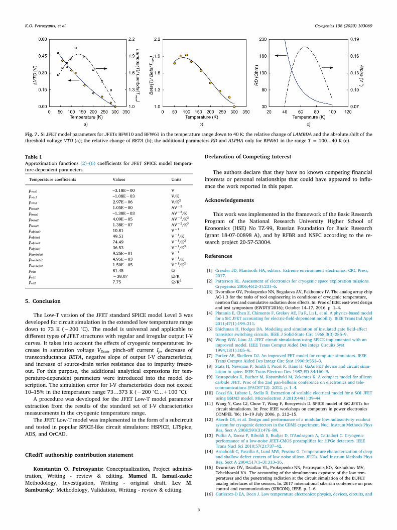
The measurement at cryogenic temperature was done with the setupat Minsk Research Instrument Making Institute [19]. In the core of thesetup is a chamber with a DUT (device under test) (see Fig. 6). Thesample was mounted on a tall steel bar that was immersed into a Dewarwith liquid nitrogen with temperature around 77 K. The bar inside thebarrel was moved up and down to adjust the temperature. The tran-sistor’s temperature was monitored using a copper-copel (type M)thermocouple. The external end of the thermocouple was placed in theglass with water and floating ice. The thermal emf of the thermocouplewas measured by the voltmeter and transferred to the PC. At every set-point temperature value, its variation during electrical measurementswas no larger than 1–2 K.
The electrical connections to the sample were made with long cablesthat were attached to a window on the top. The dipstick consists of a
steel pipe with a breakout box for cables placed at the top end and achip-holder at the lower end of the pipe. Since cables were long, a 4-wire connection [20] was used in order to exclude the voltage dropinfluence in wires between the signal generator and the DUT.
Measurement of JFET electrical characteristics was performed usingKeithley 2602 source-meter units (SMU). The measurements were car-ried out automatically under the control of the LabVIEW software.
4. Si JFET model parameters extraction in the cryogenictemperature range
To determine the set of parameters for the proposed JFET SPICEmodel in the extended temperature range, we have developed an au-tomated hardware-software subsystem that performs the followingtasks [18]:
1. Measurement of the standard set of I-V and C-V characteristics forJFET at different values of temperature { Ti }.
2. Determination of the complete set of JFET model parameters(level = 3) based on experimental measurement data obtained atroom temperature. The method of parameter identification uses acombination of analytical and optimization procedures.
3. From the complete set of model parameters, a list of the maintemperature-dependent parameters is selected: VTO, BETA,LAMBDA, ALPHA, and RD.
4. For each temperature value Ti, the corresponding values of the se-lected model parameters are determined based on the measurementresults. This procedure is automatically repeated for all planneddiscrete values of temperature Ti: i = 1…n in the range 300…40 K.
5. The table dependencies of the selected model parameters on tem-perature obtained in step 4 are approximated by analytical functionsof the form (2)–(6); the coefficients of such functions constitute theset of additional temperature parameters of the JFET model. Exactadjustment of temperature parameter values is performed usingglobal optimization, i.e. involving all available experimental char-acteristics. The temperature dependences of the parameters BETA,VTO, LAMBDA, ALPHA, and RD are shown in Fig. 7a and b; thecorresponding coefficients are listed in Table 1.
6. The analytical expressions for the parameters (see Fig. 7) obtainedin step 5, along with the coefficients, are embedded in the de-scription of the JFET SPICE model.
The proposed procedure employs two industrial tools: the SPICEmodel extraction package IC-CAP, as well as data acquisition, instru-ment control and automation package LabVIEW. The extraction pro-cedure provides the benefit of obtaining model parameters for inter-mediate temperature values.
Fig. 5. Measured and simulated output I-V characteristics of low-power p-JFETin the temperature range 73…153 K using the Low-T model (symbols – mea-surements, lines – simulation). RMS error is not more than 10%
Fig. 6. Hardware subsystem setup for JFET electrical characteristics measurement at low temperature.
K.O. Petrosyants, et al. Cryogenics 108 (2020) 103069
4
5. Conclusion
The Low-T version of the JFET standard SPICE model Level 3 wasdeveloped for circuit simulation in the extended low temperature rangedown to 73 K (−200 °C). The model is universal and applicable todifferent types of JFET structures with regular and irregular output I-Vcurves. It takes into account the effects of cryogenic temperatures: in-crease in saturation voltage VDsat, pinch-off current Ip, decrease oftransconductance BETA, negative slope of output I-V characteristics,and increase of source-drain series resistance due to impurity freeze-out. For this purpose, the additional analytical expressions for tem-perature-dependent parameters were introduced into the model de-scription. The simulation error for I-V characteristics does not exceed10–15% in the temperature range 73…373 K (−200 °C…+100 °C).
A procedure was developed for the JFET Low-T model parameterextraction from the results of the standard set of I-V characteristicsmeasurements in the cryogenic temperature range.
The JFET Low-T model was implemented in the form of a subcircuitand tested in popular SPICE-like circuit simulators: HSPICE, LTSpice,ADS, and OrCAD.
CRediT authorship contribution statement
Konstantin O. Petrosyants: Conceptualization, Project adminis-tration, Writing - review & editing. Mamed R. Ismail-zade:Methodology, Investigation, Writing - original draft. Lev M.Sambursky: Methodology, Validation, Writing - review & editing.
Declaration of Competing Interest
The authors declare that they have no known competing financialinterests or personal relationships that could have appeared to influ-ence the work reported in this paper.
Acknowledgements
This work was implemented in the framework of the Basic ResearchProgram of the National Research University Higher School ofEconomics (HSE) No TZ-99, Russian Foundation for Basic Research(grant 18-07-00898 A), and by RFBR and NSFC according to the re-search project 20-57-53004.
References
[1] Cressler JD, Mantooth HA, editors. Extreme environment electronics. CRC Press;2017.
[2] Patterson RL. Assessment of electronics for cryogenic space exploration missions.Cryogenics 2006;46(2–3):231–6.
[3] Dvornikov OV, Prokopenko NN, Bugakova AV, Pakhomov IV. The analog array chipAC-1.3 for the tasks of tool engineering in conditions of cryogenic temperature,neutron flux and cumulative radiation dose effects. In: Proc of IEEE east-west designand test symposium (EWDTS’2016); October 14–17, 2016. p. 1–4.
[4] Platania E, Chen Z, Chimento F, Grekov AE, Fu R, Lu L, et al. A physics-based modelfor a SiC JFET accounting for electric-field-dependent mobility. IEEE Trans Ind Appl2011;47(1):199–211.
[5] Shichman H, Hodges DA. Modeling and simulation of insulated gate field-effecttransistor switching circuits. IEEE J Solid-State Circ 1968;3(3):285–9.
[6] Wong WW, Liou JJ. JFET circuit simulations using SPICE implemented with animproved model. IEEE Trans Comput Aided Des Integr Circuits Syst1994;13(1):105–9.
[7] Parker AE, Skellern DJ. An improved FET model for computer simulators. IEEETrans Comput Aided Des Integr Circ Syst 1990;9:551–3.
[8] Statz H, Newman P, Smith I, Pucel R, Haus H. GaAs FET device and circuit simu-lation in spice. IEEE Trans Electron Dev 1987;ED-34:160–9.
[9] Kostopoulos K, Bucher M, Kayambaki M, Zekentes K. A compact model for siliconcarbide JFET. Proc of the 2nd pan-hellenic conference on electronics and tele-communications (PACET'12). 2012. p. 1–4.
[10] Cozzi SA, Labate L, Stella R. Extraction of scalable electrical model for a SOI JFETusing BSIM3 model. Microelectron J 2013;44(1):39–44.
[11] Wang Y, Cass CJ, Chow T, Wang F, Boroyevich D. SPICE model of SiC JFETs forcircuit simulations. In: Proc IEEE workshops on computers in power electronicsCOMPEL ’06; 16–19 July 2006. p. 212–15.
[12] Akerib DS, et al. Design and performance of a modular low-radioactivity readoutsystem for cryogenic detectors in the CDMS experiment. Nucl InstrumMethods PhysRes, Sect A 2008;591(3):476–89.
[13] Pullia A, Zocca F, Riboldi S, Budjas D, D'Andragora A, Cattadori C. Cryogenicperformance of a low-noise JFET-CMOS preamplifier for HPGe detectors. IEEETrans Nucl Sci 2010;57(2):737–42.
[14] Arnaboldi C, Fascilla A, Lund MW, Pessina G. Temperature characterization of deepand shallow defect centers of low noise silicon JFETs. Nucl Instrum Methods PhysRes, Sect A 2004;517(1–3):313–36.
[15] Dvornikov OV, Dziatlau VL, Prokopenko NN, Petrosyants KO, Kozhukhov MV,Tchekhovski VA. The accounting of the simultaneous exposure of the low tem-peratures and the penetrating radiation at the circuit simulation of the BiJFETanalog interfaces of the sensors. In: 2017 international siberian conference on proccontrol and communications (SIBCON), IEEE. p. 1–6.
[16] Gutierrez-D EA, Deen J. Low temperature electronics: physics, devices, circuits, and
Fig. 7. Si JFET model parameters for JFETs BFW10 and BFW61 in the temperature range down to 40 K: the relative change of LAMBDA and the absolute shift of thethreshold voltage VTO (a); the relative change of BETA (b); the additional parameters RD and ALPHA only for BFW61 in the range T = 100…40 K (c).
Table 1Approximation functions (2)–(6) coefficients for JFET SPICE model tempera-ture-dependent parameters.
Temperature coefficients Values Units
pvto0 –3.18E−00 Vpvto1 –1.08E−03 V/Kpvto2 2.97E−06 V/K2
pbeta0 1.05E−00 AV−2
pbeta1 –1.38E−03 AV−2/Kpbeta2 4.09E−05 AV−2/K2
pbeta3 1.38E−07 AV−2/K3
palpha0 10.81 V−1
palpha1 49.51 V−1/Kpalpha2 74.49 V−1/K2
palpha3 36.53 V−1/K3
plambda0 9.25E−01 V−1
plambda1 4.95E−03 V−1/Kplambda2 1.50E−05 V−1/K2
prd0 81.45 Ωprd1 −38.07 Ω/Kprd2 7.75 Ω/K2
K.O. Petrosyants, et al. Cryogenics 108 (2020) 103069
5
applications. Academic Press; 2000.[17] Sreelakshmi K, Satyam M. Estimation of low temperature characteristics of JFETs
from their room-temperature characteristics. Cryogenics 1996;36(5):325–31.[18] Petrosyants KO, Ismail-zade MR, Sambursky LM, Dvornikov OV, Lvov BG,
Kharitonov IA. Automation of parameter extraction procedure for Si JFET SPICEmodel in the −200…+110°C temperature range. In: 2018 Moscow Workshop onproc of electronic and networking technologies (MWENT). IEEE; 2018, March.p. 1–5.
[19] Dvornikov OV, Dziatlau VL, Prokopenko NN. Software and hardware complex forstudying semiconductor devices at low, incl. cryogenic, temperatures. In: 2017 2ndinternational ural conference on measurements (UralCon). IEEE; 2017, October. p.253–8.
[20] Petrosyants KO, Kharitonov IA, Sambursky LM, Kozhukhov MV. IV–characteristicsmeasurement error resulting from long cables for irradiated bipolar junction tran-sistors. Adv Mater Res 2015;1083:185–9.
K.O. Petrosyants, et al. Cryogenics 108 (2020) 103069
6
Related Documents