1 Compact, Lightweight and Power Efficient Voltage Tunable Multiferroic RF/Microwave Components A Dissertation Presented by Xi Yang To The Department of Electrical and Computer Engineering in partial fulfillment of the requirements for the degree of Doctor of Philosophy in the field of Electrical Engineering Northeastern University Boston, Massachusetts May, 2013

Welcome message from author
This document is posted to help you gain knowledge. Please leave a comment to let me know what you think about it! Share it to your friends and learn new things together.
Transcript

1
Compact, Lightweight and Power Efficient Voltage Tunable
Multiferroic RF/Microwave Components
A Dissertation Presented
by
Xi Yang
To
The Department of Electrical and Computer Engineering
in partial fulfillment of the requirements
for the degree of
Doctor of Philosophy
in the field of
Electrical Engineering
Northeastern University
Boston, Massachusetts
May, 2013

2
Acknowledgments
I would like to thank my advisor Professor Nian-Xiang Sun, for his
constant support and patient guidance to my research. His enthusiasm
and vision to his career always inspires me. Our collaboration is an
invaluable experience to me, from which I have learnt a lot of being a
better researcher.
I would like to thank Professor Philip E. Serafim and Professor
Edwin Marengo for being on my committee. Their advices to my thesis
are invaluable. Working with them is a happy experience I would always
like to memorize.
I would like to thank my co-workers, Dr. Jing Wu, Dr. Ming Liu,
Dr. Guomin Yang, Dr. Xing Xing, Dr. Jing Lou, Yuan Gao, Ziyao Zhou,
Shawn Beghun, Tianxiang Nan, etc. for their grateful help and
suggestion to my research.
I am grateful to Dr. Jerome J. Green for the helpful discussion on
the mechanism of partially magnetized ferrite, which helps me
understand in deep to its physical basis and the application to RF
components.
Finally, I would like to show my gratitude to my family for their
unconditional love and support they have given me through these years.

3
Abstract
In this dissertation, the knowledge of the partially magnetized ferrite concept
and magnetoelectric coupling is discussed. The partially magnetized ferrite is able to
operate in a very low permeability range less than unity with a low bias magnetic
field, which is usually less than 100 Oe. The rapid fraction variation of the
permeability will result in a large tunability in device application as the frequency
response is closely related to the change of permeability. The magnetoelectric
coupling of the ferrite can produce an effective magnetic field inside the material
which gives rise to the anisotropy tuning with the absence of the external magnetic
bias. However, this effective magnetic field is usually at the level of several 10’s Oe
which is fairly weak in getting large frequency domain tuning of the device. Thus, a
combination of both concepts is presented throughout this dissertation, which gives
a great opportunity in achieving voltage tunable microwave devices with large
tunability.
A method of measuring the complex permeability using a CPW and a
network analyzer is presented. The permeability spectra under varied magnetic
field is discussed. The measured permeability spectra show a negative region which
prohibits the wave propagation. Therefore, the energy of the RF source dissipated in
the material, and the attenuation depends on the magnitude of the negative value. In

4
addition, a resonator was fabricated on the ferrite substrate. The device showed an
absorption band gap under a magnetic field from 200 Oe to 600 Oe, which was in
good agreement with the measured permeability spectra.
A planar compact bandpass filter at C-band on a partially magnetized YIG
substrate was demonstrated with a large tunability of 380 MHz (6.1%), a low
insertion loss of 1.1 dB to 1.25 dB under low magnetic field of 0 to 100 Oe. The
bandpass filter on unsaturated ferrite substrate also showed IP1dB up to 18 dBm and
over 30 dBm in saturated state. A Ku-band multiferroic tunable bandpass filter on
nikel spinel with an electrical tunability of 270 MHz (2.1%) is presented. The
experiment discussed the usage of the spinel’s high magnetostriction in microwave
devices. The frequency tunability is closely related to the ferrite permeability
operating region. In addition, the measured central frequency under varied electric
field showed a “butterfly” behavior due to the magnetic hysteresis of the nickel
ferrite substrate in response to the PMN-PT single crystal.
A planar compact phase shifter at C-band on partially magnetized YIG
substrate was demonstrated with a large differential phase shift of 350º at 6 GHz, a
low insertion loss of 3.6 dB to 5.1 dB under a low magnetic field of 0 to 100 Oe. The
phase shift exhibited a maximum of 72 degree/decibel loss at 6.55 GHz. Electrically

5
tunable multiferroic phase shifters presented a differential phase shift up to 94º with
1-layer PMN-PT/ferrite structure, and over 115º on a stacked 2-layer PMN-
PT/ferrite structure operating in bending modes. The result is improved by 20%.
The device is able to operate without any magnetic bias and this leads to devices that
are more compact and power efficient.

6
List of Figures
Fig. 1.1 Demagnetizing field investigation of a thin ferrite plate with (a) normal and (b)
tangential external magnetic bias. .......................................................................... 21
Fig. 1.2 Remanant magnetization of YIG and Nickel spinel. ........................................... 22
Fig. 1.3 The relationship between multiferroic and magnetoelectric materials. – The
relationship between multiferroic and magnetoelectric materials. ......................... 23
Fig. 2.1 Deposition mechanism and PVD sputtering system ............................................ 32
Fig. 2.2 Spin coating process and Laurell spin coater. ...................................................... 33
Fig. 2.3 Quintel mask aligner and exposure process. ........................................................ 34
Fig. 2.4 Network analyzer Aligent PNA E8364A ............................................................. 35
Fig. 2.5 Model SR830 DSP Lock-In Amplifier from Stanford research systems. ............ 36
Fig. 3.1 GdIG (a) magnetizing approach and (b) B-H loop [1]. ........................................ 38
Fig. 3.2 Domains with magnetization parallel or anti-parallel to z – direction. ................ 39
Fig. 3.3 A simplified domain configuration with concentric cylindrical structure. .......... 42
Fig. 3.4 Measured real part of permeability of ferrite in demagnetized state. .................. 44
Fig. 3.5 µ0’ versus γ4πM0/ω for various Tran Tech garnets .............................................. 46
Fig. 3.6 Theoretical curve versus measured scatters. ........................................................ 49
Fig. 3.7 Pathways between electrical, magnetic, and elastic phase – Phase control in
ferroics and multiferroics ....................................................................................... 50
Fig. 3.8 A schematic of ME effect on a ferrite-piezoelectric multiferroic structure. ........ 52
Fig. 4.1 Schematic of measurement setup. ........................................................................ 57
Fig. 4.2 Ferrite perturbation of CPW circuits in different states. (a) S21, and (b) S11. ... 61
Fig. 4.3 Measured complex permeability of the ferrite (a) real part, and (b) imaginary part.
................................................................................................................................ 64
Fig. 4.4 Measured normalized magnetic hysteresis loop of the doped YIG sample. ........ 64
Fig. 4.5 Narrow band FMR measurement of the ferrite. ................................................... 66
Fig. 4.6 Measured transmission coefficients (S21) and reflection ceofficients (S11). ..... 68
Fig. 4.7 Measured s-parameters (S21 and S11) under 200 Oe, 400 Oe and 600 Oe. ........ 70

7
Fig. 4.8 Measured insertion loss under varied magnetic bias. .......................................... 71
Fig. 5.1 Magnetoelectric microwave bandpass filter. (a) Device schematic and (b)
measured S21 parameter......................................................................................... 78
Fig. 5.2 Dual H- and E-field tunable bandpass filter. ........................................................ 80
Fig. 5.3 Magnetically tunable superconducting bandpass filter (a) device schematic and
(b) S21 parameters. ................................................................................................. 83
Fig. 5.4 (a) Geometry of the bandpass filter on YIG substrate and (b) fabricated device. 85
Fig. 5.5 Calculated real part of complex permeability under varied magnetic biases in
partially magnetized states. .................................................................................... 87
Fig. 5.6 Simulated performance of the proposed bandpass filter (a) transmission and (b)
reflection. ................................................................................................................ 88
Fig. 5.7 A comparison between simulation and measurement at zero magnetic bias. ...... 90
Fig. 5.8 Measured (a) transmission (b) reflection coefficients under different magnetizing
fields. ...................................................................................................................... 92
Fig. 5.9 Central frequency of the tunable bandpass filter under magnetic field from -100
Oe to 100 Oe. .......................................................................................................... 93
Fig. 5.10 Schematic of the high power measurement set up. ............................................ 97
Fig. 5.11 Measured power handling capability of the bandpass filter in partially
magnetized and saturated states. ............................................................................ 97
Fig. 5.12 Magnetic hysteresis loop of TT86-6000 nickel ferrite. .................................... 100
Fig. 5.13 Geometry of the bandpass filter. ...................................................................... 101
Fig. 5.14 Measured (a) transmission and (b) reflection coefficients under different
magnetizing fields. ............................................................................................... 102
Fig. 5.15 A frequency distribution versus magnetic bias at a lower frequency. ............. 103
Fig. 5.16 (a) Diagram showing the device with ferrite/PMN-PT multiferroic
heterostructure, and (b) fabricated device. ........................................................... 105
Fig. 5.17 Measured E-field tunable operating frequency range of the bandpass filter under
different magnetic bias fields, showing the dual E- and H-field tunability. ........ 108
Fig. 5.18 S21 curves of the multiferroic device under 100 Oe magnetic bias. ............... 108

8
Fig. 5.19 Central resonant frequency show “butterfly” behavior. ................................... 110
Fig. 6.1 (a) Schematic of the phase shifter with ME element (b) permeability dispersion,
and (c) phase shift test result at X-band. .............................................................. 121
Fig. 6.2 Wave propagation, signal RF magnetic field and magnetization configuration.
.............................................................................................................................. 123
Fig. 6.3 (a) Geometry of meander line phase shifter and (b) fabricated device on YIG
substrate with PMN-PT bonding. ......................................................................... 126
Fig. 6.4 (a) Geometry of the phase shifter and layer demonstration, (b) fabricated device
with fixture. .......................................................................................................... 129
Fig. 6.5 Simulated (a) transmission and (b) reflection coefficients of the meander line
ferrite phase shifter. .............................................................................................. 131
Fig. 6.6 Simulated transmission and reflection coefficients of double spiral phase shifter.
.............................................................................................................................. 132
Fig. 6.7 Calculated phase shift of the meander line phase shifter. .................................. 133
Fig. 6.8 A fitted hysteresis loop curve of the ferrite substrate obtained from measured
phase shift. ............................................................................................................ 134
Fig. 6.9 Transmission and reflection of the phase shifter under varied magnetic bias. .. 136
Fig. 6.10 Measured (colored lines) and calculated (colored scatters) phase shift under
varied magnetic bias. ............................................................................................ 137
Fig. 6.11 Phase shift per insertion loss of the phase shifter. ........................................... 138
Fig. 6.12 Measured (a) transmission coefficient and (b) reflection coefficient under varied
electric field. ......................................................................................................... 141
Fig. 6.13 Measured differential phase shift of the multiferroic phase shifter with meander
line structure. ........................................................................................................ 142
Fig. 6.14 Measured differential phase shift of the phase shifter with 1-layer PMN-PT
plate. ..................................................................................................................... 144
Fig. 6.15 (a) Measured differential phase shift with stacked 2-layer PMN-PT. (b) Stacked
2-layer PMN-PT bending mode demonstration. .................................................. 146
Fig. 6.16 Measured and simulated s-parameters of the designed phase shifter. ............. 147

9
Table of Contents
Abstract ..................................................................................................................... 3
List of Figures ........................................................................................................... 6
Chapter 1 : Introduction ......................................................................................... 13
1.1. Background............................................................................................. 14
1.2. Microwave ferrites.................................................................................. 15
1.3. Microwave and magnetic properties ...................................................... 17
1.3.1. Permeability tensor ............................................................................ 17
1.3.2. Demagnetizing field ........................................................................... 19
1.3.3. Remanant magnetization .................................................................... 21
1.4. Multiferroics ........................................................................................... 22
1.5. Dissertation overview ............................................................................. 24
1.6. References .............................................................................................. 27
Chapter 2 : Simulation, Fabrication and Measurement Setups ............................. 29
2.1. High Frequency Structural Simulator (HFSS) ....................................... 29
2.2. Fabrication facilities ............................................................................... 30
2.2.1. Physical Vapor Deposition (PVD) system ......................................... 31
2.2.2. Laurell spinner for spin coating ......................................................... 32
2.2.3. Quintel 4000 Mask Aligner ............................................................... 33
10
2.3. Measurement tools.................................................................................. 34
2.3.1. Vector Network Analyzer (VNA) ...................................................... 34
2.3.2. Lock-in Amplifier .............................................................................. 36
2.4. References .............................................................................................. 36
Chapter 3 : Theory of Partially Magnetized Ferrite and ME Coupling ................. 37
3.1. Partially magnetized ferrites ................................................................... 37
3.1.1. Schlomann‟s model ............................................................................ 38
3.1.2. Naito‟s model ..................................................................................... 46
3.1.3. Summary ............................................................................................ 49
3.2. Magnetoelectric (ME) coupling ............................................................. 50
3.3. Conclusion .............................................................................................. 52
3.4. References .............................................................................................. 54
Chapter 4 : Ferrite Substrate Based Resonator...................................................... 56
4.1. Permeability prediction background ...................................................... 56
4.2. Magnetic properties measurements ........................................................ 59
4.2.1. Magnetic permeability broad-band measurement .............................. 59
4.2.2. Magnetic hysteresis loop .................................................................... 64
4.2.3. Ferromagnetic resonant frequency (FMR) ......................................... 65
4.3. Resonator measurement verification ...................................................... 66
11
4.4. Conclusion .............................................................................................. 71
4.5. Reference ................................................................................................ 73
Chapter 5 : Multiferroic BPF on Partially Magnetized Ferrite ............................. 75
5.1. Motivation .............................................................................................. 75
5.2. Introduction to multiferroic tunable bandpass filters ............................. 76
5.3. Magnetically tunable BPF based on partially magnetized ferrite .......... 81
5.3.1. Research efforts on BPF using partially magnetized ferrites ............ 81
5.3.2. Device construction ............................................................................ 83
5.3.3. Simulations and experimental verification ........................................ 85
5.3.4. Power handling capability test ........................................................... 96
5.3.5. Summary of magnetically tunable BPF ............................................. 98
5.4. Multiferroic tunable bandpass filters ...................................................... 98
5.4.1. Bandpass filter on Nickel ferrite substrate ......................................... 99
5.4.2. Ni-ferrite/PMN-PT Multiferroic heterostructure ............................. 104
5.4.3. Measurement verification ................................................................ 106
5.5. Conclusion ............................................................................................ 110
5.6. References ............................................................................................ 112
Chapter 6 : Voltage Tunable Multiferroic Phase Shifter ...................................... 115
6.1. Introduction to phase shifters ............................................................... 116

12
6.1.1. State of art of tunable phase shifters ................................................ 117
6.1.2. Application of ferrites in tunable phase shifters .............................. 118
6.2. Propagation constant in ferrites ............................................................ 121
6.3. Device construction .............................................................................. 125
6.3.1. Meander line phase shifter with YIG/PMN-PT bilayer ................... 125
6.3.2. Phase shifter with stack 2-layer PMN-PT/YIG structure ................ 127
6.4. Simulation............................................................................................. 130
6.5. Numerical results .................................................................................. 132
6.6. Measurement verification ..................................................................... 135
6.6.1. Meander line phase shifter ............................................................... 135
6.6.2. Double spiral phase shifter ............................................................... 143
6.7. Conclusion ............................................................................................ 148
6.8. References ............................................................................................ 150
Chapter 7 : Conclusion ......................................................................................... 153

13
Chapter 1 : Introduction
Modern ultra wideband communication systems, radars, and metrology systems all
need reconfigurable subsystems that are compact, low loss, small form factor, and power
efficient [1]. Ferrite has been applied in RF/microwave devices for more than half a
century due to the low-loss, high power, high resolution, and high reliability.
For the application of ferrites in tunable devices, one usually takes the advantage
of magnetic property influence of the wave propagating characteristic. A simplest
example is the phase shift of a ferrite-loaded transmission line that can be controlled by
the magnetization of the ferrite ceramics. [2] Similarly, tunable ferrite bandpass filters [3-
5], phase shifters [6-8], isolators [9], and circulators [10] have drawn attention to many
researchers. Typically, the study of the magnetic properties of magnetic materials or
ferrites would allow one to have a better understanding of the wave propagation in
magnetic media and a thorough prediction of the performances of the microwave devices.
Conventionally, ferrites and magnetic materials are tuned by magnetic field. In the
past 10 years, multiferroics consisting of multiple order parameters and cross-coupling
between the orders provide an alternative to tune the magnetic properties or anisotropies
with electric fields [11], which has been of great interests in microwave tunable devices
[12, 13]. This dissertation theoretically and experimentally focuses on the magnetic

14
properties of the ferrite materials, wave propagation in magnetic media, and multiferroics
application in microwave devices.
1.1. Background
The essential concept throughout this dissertation is based on Maxwell‟s equation
which gives a general form of electromagnetic (EM) wave propagation in a medium [14]
Gauss‟s law (1.1a)
Gauss‟s law of magnetism (1.1b)
Faraday‟s law
(1.1c)
Ampere‟s law
(1.1d)
where
is the charge density ( )
B is the magnetic flux density ( )
J is the current density ( )
and are permeability ( ) and permittivity ( )

15
In real media, the permeability is a tensor due to the anisotropic and dispersive
characteristics of the medium, in particular, yields
[
] (1.2)
For an anisotropic, inhomogeneous, and dispersive medium, the elements in the
tensor are complex, and have frequency and spatial dependence. In this dissertation, we
will focus on the tensor nature of the permeability, and discuss the interaction between
the magnetic materials and the EM wave propagation.
1.2. Microwave ferrites
Low loss ferromagnetic materials, or ferrites are widely used in passive
RF/microwave components. The magnetic resonances of the components can be tuned
over a wide frequency range using magnetic fields. There are basically three types of
ferrites: hexaferrites, garnets, and spinels.
Hexaferrites have a hexagonal crystal structure and with a large saturation
magnetization ( ) and a large magnetocrystalline uniaxial anisotropy ( ), and will
bias the ferrite to high frequencies, such as Ku band. In particular, M-type (BaFe12O19)
ferrites has an out of plane easy axis of magnetization which led to many circulator
designs [2].

16
Garnets, as a class of very low loss material, have been applied in RF/microwave
devices for many years. The first study of the cubic crystal structure of garnets is due to
Menzer. Bertaut and Forrat prepared the most well-known garnet yttrium iron garnet
(Y3Fe5O12, or YIG). The YIG material exhibits very low loss at high frequencies. The
ferromagnetic resonant (FMR) linewidth ( ) of a typical YIG is measured to be less
than 1 Oe single crystals, and 25 Oe for polycrystallines. The can be varied from
1200 Gauss to more than 2000 Gauss with different doping composites. Therefore, the
materials show great merit in military or commercial communication systems.
Although spinels exhibit a large initial permeability, the value drops very quickly
with the increase of frequency. In addition, the spinels are known as high relaxation loss
materials with a typical ferromagnetic loss ( ) over 150 Oe. The material is not
comparable with garnets in microwave applications. However, the introducing of
magnetoelectric (ME) coupling recently through electric fields is more attractive than
magnetic control of magnetism which gives rise to the study on spinels. The saturation
magnetostriction ( ) can be as high as several ten‟s ppm which show great potential of
achieving voltage control of magnetism. [15] For example, Nickel spinel has a of 25
ppm compared to YIG garnet of -1~2 ppm.
17
1.3. Microwave and magnetic properties
1.3.1. Permeability tensor
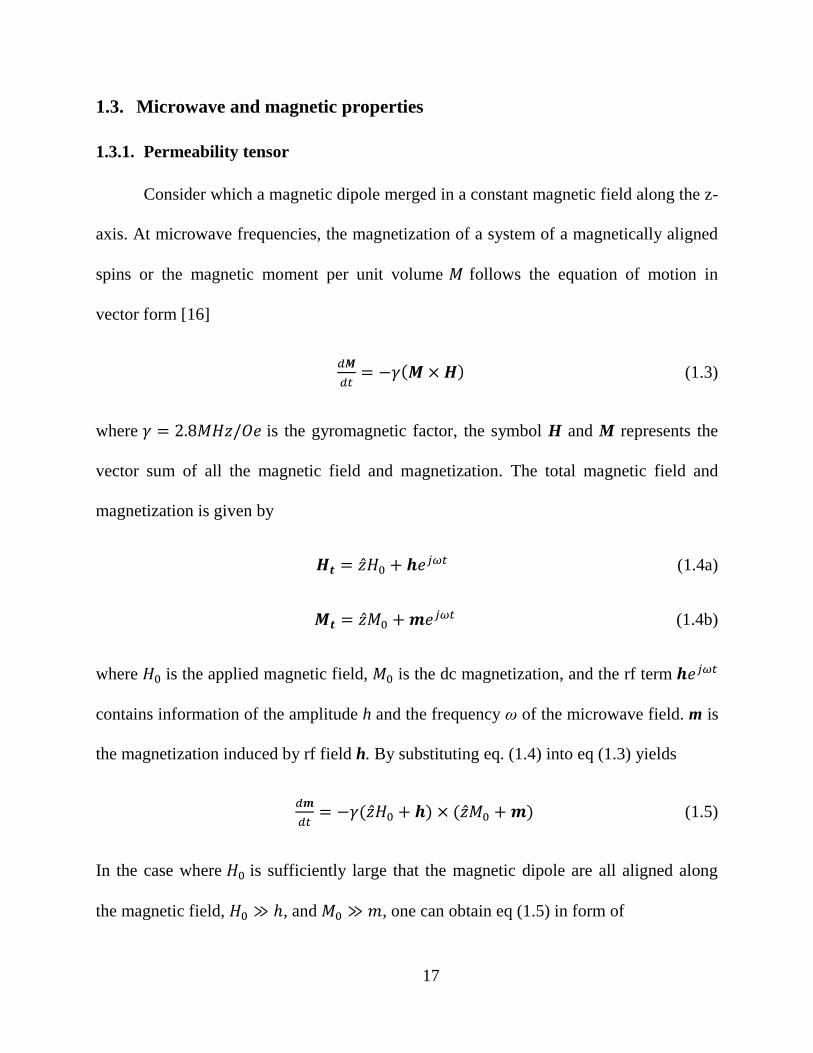
Consider which a magnetic dipole merged in a constant magnetic field along the z-
axis. At microwave frequencies, the magnetization of a system of a magnetically aligned
spins or the magnetic moment per unit volume follows the equation of motion in
vector form [16]
( ) (1.3)
where is the gyromagnetic factor, the symbol H and M represents the
vector sum of all the magnetic field and magnetization. The total magnetic field and
magnetization is given by
(1.4a)
(1.4b)
where is the applied magnetic field, is the dc magnetization, and the rf term
contains information of the amplitude h and the frequency ω of the microwave field. m is
the magnetization induced by rf field h. By substituting eq. (1.4) into eq (1.3) yields
( ) ( ) (1.5)
In the case where is sufficiently large that the magnetic dipole are all aligned along
the magnetic field, , and , one can obtain eq (1.5) in form of

18
{
(1.6)
where , and . Take derivative over time on both sides of eq (1.6)
yields
2(
)
( )
, (1.7a)
or [
] (1.7b)
where
,
. Knowing the relation ( ),
the tensor permeability in saturated case then can be written as
[
] [
] (1.8)
where
For the case H0 is not sufficiently large, the materials is unsaturated, the elements
in tensor permeability follows a more complicated expression. This will be discussed in
chapter 3.

19
1.3.2. Demagnetizing field
Magnetic materials show an intrinsic field to oppose the external magnetic field. It
is produced by the surface magnetic charge on the interface between the magnetic and
nonmagnetic material. Consider a finite ferrite thin plate with z-axis normal to the board
(Fig. 1.1a). The magnetic field is applied either along z-axis or in-plane. Assume all the
magnetic moment is aligned along the magnetization direction. If the magnetic field is
applied along the z-axis, Gauss‟s law gives
, (1.9a)
, ( in air) (1.9b)
(1.9c)
where is the internal field, is the applied external magnetic bias, and is the
magnetization along the z-axis. Eq (1.9a-c) yields
(1.10)
From eq (1.10) one obtains the demagnetizing field of a ferrite plate with z-axis normal to
the board face is , and the z-axis demagnetizing factor is .
Similarly, for a tangential external magnetic bias (fig. 1.1b), the magnetic field
needs to be continuous at the interface of the magnetic and nonmagnetic surface, giveing

20
(1.11)
Therefore, one can conclude the x- and y-axis demagnetizing factor for a thin plate is
.
(a)

21
(b)
Fig. 1.1 Demagnetizing field investigation of a thin ferrite plate with (a) normal
and (b) tangential external magnetic bias.
1.3.3. Remanant magnetization
After the ferrite is magnetized to saturation, the magnetization will relax to a
remanant magnetization ( ) with the absence of the external magnetic bias. For YIG
and Nickel spinel, the is quite small. (Fig. 1.2) However, for M-type strontium
hexaferrite with an out of plane easy magnetization, the may be as large as 3500
Gauss, hence is a good candidate for self-biased junction circulators [2]. It has also been
used in many latching wire devices [17].

22
Fig. 1.2 Remanant magnetization of YIG and Nickel spinel.
1.4. Multiferroics
Multiferroics have been formally defined as materials that exhibit more than one
primary ferroic order parameter simultaneously. Fig 1.3 shows the relationship between
multiferroic and magnetoelectric materials [18]. The red area represents materials that are
multiferroic. As independent orders, magnetization and polarization in multiferroics is
able to realize four logic states and enhance the functionality in multiferroic devices. But
in practice, besides both independent orders, the cross-coupling between them would be
more attractive, since it reveals a dual-tunable capability that is a dielectric polarization
variation in response to an applied magnetic field, or an induced magnetization from an
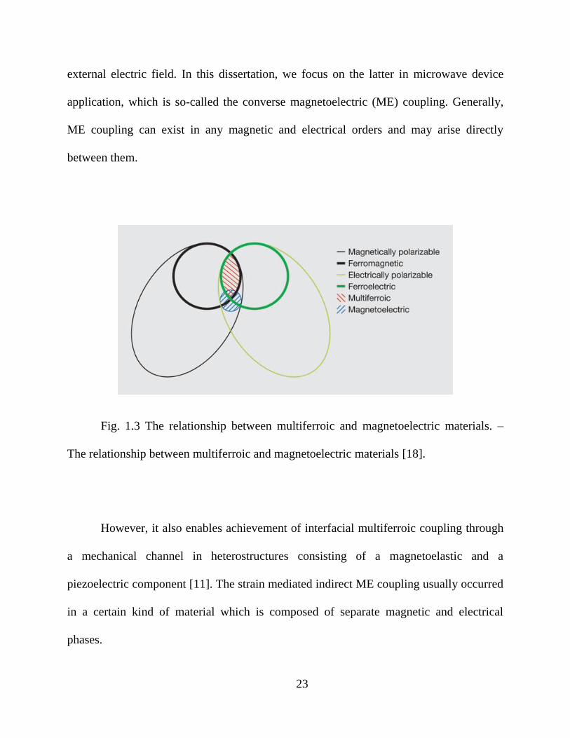
23
external electric field. In this dissertation, we focus on the latter in microwave device
application, which is so-called the converse magnetoelectric (ME) coupling. Generally,
ME coupling can exist in any magnetic and electrical orders and may arise directly
between them.
Fig. 1.3 The relationship between multiferroic and magnetoelectric materials. –
The relationship between multiferroic and magnetoelectric materials [18].
However, it also enables achievement of interfacial multiferroic coupling through
a mechanical channel in heterostructures consisting of a magnetoelastic and a
piezoelectric component [11]. The strain mediated indirect ME coupling usually occurred
in a certain kind of material which is composed of separate magnetic and electrical
phases.

24
1.5. Dissertation overview
This dissertation focuses on the advantages of partially magnetized ferrite usage in
magnetoelectric coupling (ME) devices, the combination of these two concepts is
proposed. The magnetic permeability of partially and fully magnetized ferrite is
theoretically and experimentally studied. The EM wave propagation in ferrite media will
be discussed. In addition, voltage tunable multiferroic microwave devices such as phase
shifters and bandpass filters are implemented.
In chapter 2, I will briefly introduce the numerical modeling tools, fabrication
tools, and the measurement setups that are used throughout this dissertation. First, HFSS
software is introduced as a pre-experimental tool. Next, some key fabrication tool such as
spin coater and the mask aligner which are used to do the photolithography process are
described. Finally, the setups that are used for characterizing the fabricated devices, such
as vector network analyzer are discussed.
In chapter 3, we will provide a theoretical overview of the permeability tensor in
the states before saturation. The Schlomann‟s model and the Naito‟s model will be
introduced. Green‟s experimental results will also be discussed to verify the models‟
consistency. Furthermore, magnetoelectric coupling theory is also given for an advanced

25
application of the partially magnetized ferrites. The concept of combining the two
theories is proposed as the basis of this dissertation.
In chapter 4, the frequency and field response of the ferrite permeability in fully
saturated states will be studied. First, I will give an introduction to the research state of
art on the measurement of permeability techniques. Next, a simple but effective approach
of measuring the permeability will be described, and the experiment result of the
permeability measurement is presented. Then, a resonator on ferrite substrate is presented,
and the test frequency response is in agreement with the permeability measurement. In
addition, a prediction of the wave propagation prohibiting band gap is proved by the
negative region from the permeability measurement.
In chapter 5, bandpass filters on partially magnetized ferrite concept is introduced.
Besides, the state of art of voltage tunable multiferroic bandpass filters is discussed. To
implement a voltage tunable multiferroic bandpass filter using partially magnetized
concept, a low loss bandpass filter at C-band on YIG substrate as a startup is presented.
The bandpass filter shows a tunability of over 6% with less than 100 Oe magnetic bias,
the insertion loss is reported as low as 1.1 dB. In addition, the power handling capability
of the devices is presented with an IP1dB of 18 dBm. Nickel spinel ferrite with a high
saturation magnetostriction value of ~ -33 ppm is used for multiferroic bandpass filter at

26
KU –band. The bandpass filter shows an electric field tunability of 270 MHz through ME
coupling under a 100 Oe magnetic bias.
In chapter 6, a planar compact phase shifter at C-band on partially magnetized
YIG substrate was demonstrated with a large differential phase shift of 350º at 6 GHz, a
low insertion loss of 3.6 dB to 5.1 dB under a low magnetic field of 0 to 100 Oe. The
phase shift exhibited a maximum of 72 degree/decibel loss at 6.55 GHz. A differential
phase shift up to 94º is obtained with the PMN-PT/ferrite heterostructure. Planar
electrically tunable multiferroic phase shifter on a stacked 2-layer PMN-PT/ferrite
structure was demonstrated with a large differential phase shift over 115º under an
electric field of 11 kV/cm. The result is improved by 20% compared to 1-layer PMN-PT
design. The device is able to operate without any magnetic bias leads to devices that are
more compact and power efficient. The devices combining with multiferroic and partially
magnetized ferrite concept is promising in achieving voltage tunable devices with large
tunability.
Chapter 8 will be the conclusion.

27
1.6. References
1. Arthur J. Baden Fuller, Ferrites at Microwave Frequencies, London: Peter Peregrinus,
1987.
2. J. Wang, “Toward Self-biasd Ferrite Microwave Devices,” Thesis, 2011.
3. P. S. Cater, “Magnetically-Tunable Microwave Filters Using Single-Crystal Yttrium-
Iron-Garnet Resonators,” IEEE Trans. Microw. Theory Tech., vol. 9, no. 3, pp. 252-
260, 1961.
4. M. Tsutsumi, et al, “Magnetically Tunable Superconductor Filters Using Yttrium Iron
Garnet Films,” IEEE Trans. Magn., vol. 31, no. 6, pp. 3647-3649, 1995.
5. G. M. Yang, A. Shrabstein, X. Xing, O. Obi, S. Stoute, M. Liu, J. Lou, and N. X. Sun,
„Miniaturized Antennas and Planar Bandpass Filters With Self-Biased NiCo-Ferrite
Films‟, IEEE Trans. Magn., vol. 45, no. 10, pp. 4191-4194, 2009.
6. M. A. Popov, I. V. Zavislyak and G. Srinivasan, “Magnetic field tunable 75-110 GHz
dielectric phase shifter,” Electronics Letters, vol. 46, no. 8, pp. 569-570, April 2010.
7. X. Zuo, Ping Shi, S.A. Oliver, and C. Vittoria, “Single crystal hexaferrite phase
shifter at Ka band,” J. Appl. Phys., vol. 91, no. 10, p. 7622 , 2002.
8. A. L. Geiler, Jianwei Wang, Jin Sheng Gao, Soack Dae Yoon, Yajie Chen, Vincent G.
Harris, and Carmine Vittoria, “Low Bias Field Hexagonal Y-Type Ferrite Phase
Shifters at Ku-Band,” IEEE Trans. Magn., vol. 45, no. 10, pp. 4179-4182, Oct. 2009.
9. J. Wu, M. Li, X. Yang, S. Beguhn, and Nian X. Sun, “A Novel Tunable Planar
Isolator with Serrated Microstrip Structure,” IEEE Trans. Magn., vol. 48, no. 11, pp.
4371-4374, 2012.
28
10. J. Wang, A. Yang, Y. Chen, Z. Chen, A. Geiler, S. M. Gillette, V. G. Harris, and C.
Vittoria, “Self Biased Y-Junction Circulator at KU Band,” IEEE Microw. Wireless
Compon. Lett., vol. 21, no .6, 2011.
11. M. Liu, “E-Field tuning of magnetism in multiferroic heterostructures,” Thesis, 2010.
12. A. S. Tatarenko, and G. Srinivasan, M. I. Bichurin, “Magnetoelectric microwave
phase shifter,” Appl. Phys. Lett., vol. 88, p. 3507, 2006.
13. A. S. Tatarenko, V. Gheevarughese and G. Srinivasan, “Magnetoelectric microwave
bandpass filter,” Electronic Letters, vol. 42, no. 9, pp. 540-541, April 2006.
14. Constantine A. Balanis, Advanced engineering electromagnetics: Wiley, 2nd
edition.
15. N. X. Sun and G. Srinivasan, “Voltage Control of Magnetism in Multiferroic
Heterostructures and Devices,” SPIN, vol. 2, no. 3, p. 1240004, 2012.
16. B. Lax and K. J. Button, Microwave Ferrites and Ferrimagnetics: McGraw-Hill Book
Company, Inc., 1962.
17. G. F. Dionne, D. E. Oates, D. H. Temme, and J. A. Weiss, “Ferrite-Superconductor
Devices for Advanced Microwave Applications,” IEEE Trans. Microw. Theory Tech,
vol. 44, no.7, pp. 1361-1368, Jul. 1996.
18. W. Eerenstein, N. D. Mathur, and J.F. Scott, “Multiferroic and magnetoelectric
materials,” Nature, 442, pp. 759-765, 2006.

29
Chapter 2 : Simulation, Fabrication and Measurement Setups
In this chapter, the numerical and experimental setups for the simulation,
fabrication and measurement of the microwave devices are presented. The modeling
software High Frequency Structural Simulator (HFSS) from ANSYS will be introduced.
Some of the key fabrication equipment will be listed. In addition, the setups for the
measurement of the devices will also be covered. [1]
2.1. High Frequency Structural Simulator (HFSS)
HFSS is a commercial finite element method solver for electromagnetic structures
from ANSYS. It is one of several commercial tools used for antenna design, and the
design of complex RF electronic circuit elements including filters, transmission lines, and
packaging. Characterization of the model, such as field distribution, S-parameters,
radiation pattern, phase, resonant frequency, etc. can also be obtained from the software.
When magnetic materials, e.g. ferrites, are involved in the design, the HFSS can
only model the ferrite materials in fully saturated states, where the permeability is a
tensor [2]
(
) (2.1)

30
(
),
where for saturated case. , is the dc magnetic bias; ,
is the saturation magnetization of the ferrite, and is the signal angular frequency.
When stronger magnetic field beyond saturation is applied, the magnetization remains as
the value .
However, when the ferrite is operated in partially magnetized states, the actual
magnetization is a value between 0 and depending on the magnitude of field
applied. The diagonal element of in the tenser permeability follows a more complex
expression. Therefore, it is hard to characterize the model with respect to the change of
magnetic field in HFSS. In this dissertation, we use numerical combining with software
modeling as the simulation.
2.2. Fabrication facilities
The devices described in this dissertation do not follow the procedure for
fabrication on standard printed circuit boards (PCBs). Cleanroom and MEMS process are
involved but with a much large scale and error tolerance. Here listed some of the key
equipments that have been used in the experiments.
31
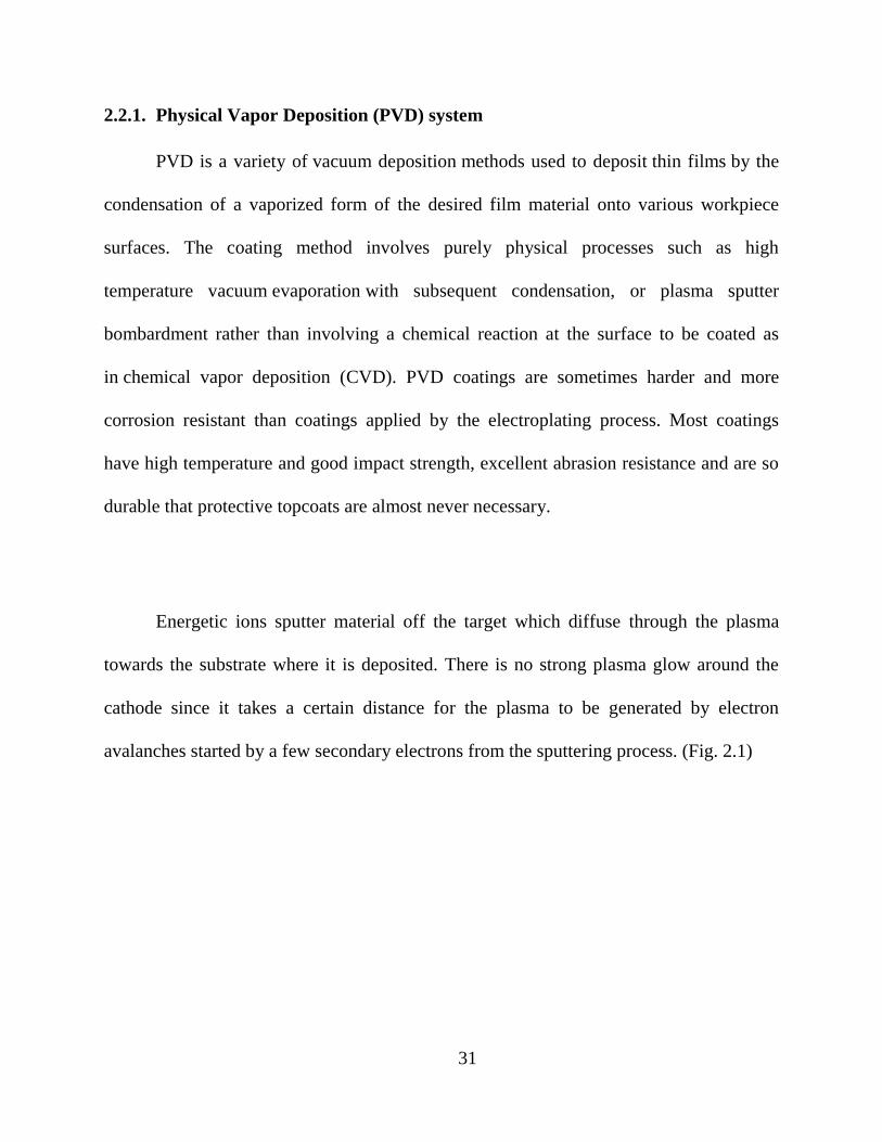
2.2.1. Physical Vapor Deposition (PVD) system
PVD is a variety of vacuum deposition methods used to deposit thin films by the
condensation of a vaporized form of the desired film material onto various workpiece
surfaces. The coating method involves purely physical processes such as high
temperature vacuum evaporation with subsequent condensation, or plasma sputter
bombardment rather than involving a chemical reaction at the surface to be coated as
in chemical vapor deposition (CVD). PVD coatings are sometimes harder and more
corrosion resistant than coatings applied by the electroplating process. Most coatings
have high temperature and good impact strength, excellent abrasion resistance and are so
durable that protective topcoats are almost never necessary.
Energetic ions sputter material off the target which diffuse through the plasma
towards the substrate where it is deposited. There is no strong plasma glow around the
cathode since it takes a certain distance for the plasma to be generated by electron
avalanches started by a few secondary electrons from the sputtering process. (Fig. 2.1)

32
Fig. 2.1 Deposition mechanism and PVD sputtering system.
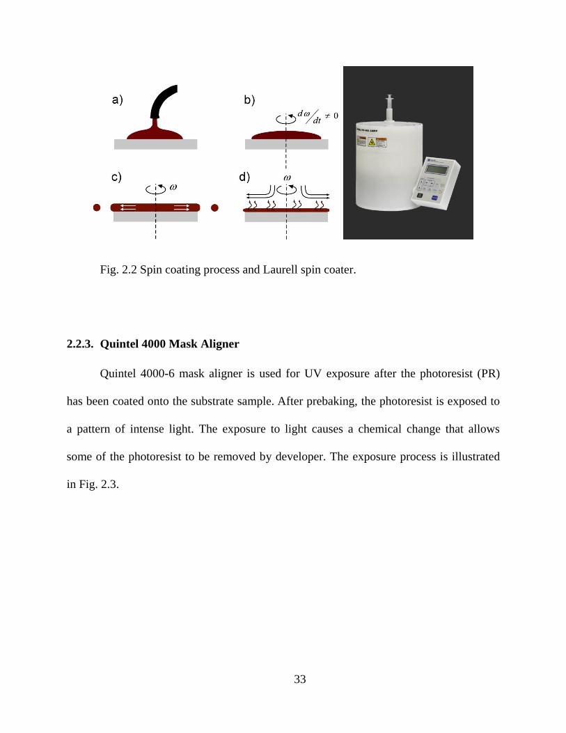
2.2.2. Laurell spinner for spin coating
Spin coating is a procedure used to apply uniform thin films to flat substrates. An
excess amount of a solution is placed on the substrate, which is then rotated at high speed
in order to spread the fluid by centrifugal force. Rotation is continued while the fluid
spins off the edges of the substrate, until the desired thickness of the film is achieved.
Spin coating is widely used in microfabrication photolithography process, to deposit
layers of photoresist.
33
Fig. 2.2 Spin coating process and Laurell spin coater.
2.2.3. Quintel 4000 Mask Aligner
Quintel 4000-6 mask aligner is used for UV exposure after the photoresist (PR)
has been coated onto the substrate sample. After prebaking, the photoresist is exposed to
a pattern of intense light. The exposure to light causes a chemical change that allows
some of the photoresist to be removed by developer. The exposure process is illustrated
in Fig. 2.3.

34
Fig. 2.3 Quintel mask aligner and exposure process.
In addition, Inductively Coupled Plasma (ICP Plasma Therm 790) and Veeco
Microetch Ion Mill are used for dry etch.
2.3. Measurement tools
2.3.1. Vector Network Analyzer (VNA)
The characterization of the microwave devices are mainly carried out by our VNA
(Aligent PNA E8364A), 45 MHz to 50 GHz. The equipment can produce a power level
up to 30 dBm, which will be used for power handling capability measurement in this
dissertation.

35
Fig. 2.4 Network analyzer Aligent PNA E8364A.

36
2.3.2. Lock-in Amplifier
The Model SR830 DSP Lock-In Amplifier (Stanford research systems) connecting
with a High-Voltage Power Amplifier (gain 1000V/V) produces a voltage of .
Fig. 2.5 Model SR830 DSP Lock-In Amplifier from Stanford research systems.
2.4. References
1. HFSS V10 user guide.
2. B. Lax and K. J. Button, Microwave Ferrites and Ferrimagnetics: McGraw-Hill Book
Company, Inc., 1962.

37
Chapter 3 : Theory of Partially Magnetized Ferrite and ME Coupling
3.1. Partially magnetized ferrites
In many of the application of ferrites in microwave devices such as phase shifters,
filters, switches, and rotators the magnetic material is only partially magnetized. The
unsaturated ferrite exhibits a low permeability value less than unity and a significant
variation is obtained with a modest field. As in Fig. 3.1, a closed path magnetic field of
10~20 Oe is able to magnetize the ferrite toroid (gadolinium yttrium iron garnet) to
saturation [1].
(a)

38
(b)
Fig. 3.1 GdIG (a) magnetizing approach and (b) B-H loop [1].
In device point of view, the fractional variation of the permeability will result in a
large change in frequency domain, since either the phase shift of a phase shifter or the
resonant frequency of a bandpass filter relies on the factor √ or √ ⁄ . Therefore,
understanding of the partially magnetized ferrite mechanism will provide a helpful
guidance to design the microwave devices.
3.1.1. Schlomann’s model
Assuming there are only two types of domains in this model, which are aligned
either parallel (“up domains”) or anti-parallel (“down domains”) to the z-axis. This
provides a cylindrical domain configuration with arbitrary cross sections in the x-y plane.
The dc magnetizing field is applied in z-direction, thus the dc magnetization is either
parallel to the z – direction (not as up domains “u”), or anti-parallel to the -z – direction
(not as down domains “d”) as shown in Fig. 3.2. In the plot, two or more “up domains” or
“down domains” are adjacent, then the domains with the same type can be combined into
one domain.

39
Fig. 3.2 Domains with magnetization parallel (“u”) or anti-parallel (“d”) to z –
direction.
The local permeability is the same throughout each type, but differs from one type
of domain to the other. Then the x and y components of the local permeability tensors for
the two types of domains can be expressed by
(
), (
) (3.1)
from equations of motion discussed in chapter 1, one can obtain

40
( ⁄ )
(3.2a)
( ⁄ )
(3.2b)
where the is the dc magnetic field strength in z – direction. Under the condition
described in [2], it is permissible to set , . If the loss is not taken into
account one can obtain
, and
where .
When an rf magnetic field h(r) is associated with some arbitrary distribution of rf
magnetization m(r), the ( ) is a gradient of a potential ( ) ( ). By knowing the
divergence of vanishes, ( ) then satisfies
* (
)
+ (3.3)
In this configuration it is z independent, thus eq (3.3) yields
(
) (3.4)
The boundary condition of an adjacent “up domain” and “down domain” requires the
normal component of b and the tangential component of h must continuous.

41
(
) (
) (3.5a)
( ) (3.5b)
where “n” and “s” represents the normal and tangential component at the interface. Eq
(3.4) should also satisfy the boundary condition at the interface between the material and
the air.
The effective circularly permeability and is given in response of the
sense of positively and negative rotation of rf magnetic field, respectively, which have
the form
(3.6)
A simplified cylindrical domain structure is used for the solution the differential
eq (3.5). The domain structures observed in x-y plane are concentric circles with “up
domain” and “down domain” periodically aligned with z – axis, as shown in Fig. 3.3. The
radii of the domains are rn (n=1, 2, 3,∙∙∙). Therefore, the solution follows the forms of
, (3.7)
where m is positive integers. Specifically, the potential of nth domain is expressed as
( ) (3.8)

42
At the core domain, . Outside the sample, to satisfy the
condition, where is the amplitude of rotated rf magnetic field.
Fig. 3.3 A simplified domain configuration with concentric cylindrical structure.
A complex mathematical calculation leads to:
(3.9)
This gives a similar result as Rado‟s model [3]. The right hand side of eq (3.9) is
independent to the domain configuration. Therefore, the minimum regardless of
domain configuration is obtained when is zero

43
*( ⁄ ) ( )
( ⁄ ) +
(3.10)
where Ha is assumed as the only anisotropy field that exists inside the materials. A
detailed calculation may be found in [2]. The discussion so far the permeability
correspond to x and y – axis, for a three dimensional case, the effective permeability
corresponds to z – axis is equaled to unity which will contribute 1/3 of the effective
permeability. Therefore, the minimum effective permeability in demagnetized state yields
*( ⁄ ) ( )
( ⁄ ) +
(3.11)
It is seen from eq (3.11), that when ( ), the is a real number;
while for ( ), has an imaginary part. This indicates that
the material will introduce addition loss. Assuming is not comparable to , the
term leaves a so-called “low field loss” condition, i.e. is close to or
great than unity. The calculated curve in terms of fits the measurement result for
different types of ferrites [4], as shown in Fig 3.4.

44
Fig. 3.4 Measured real part of permeability of ferrite in demagnetized state. –
versus . [4]

45

46
Fig. 3.5 versus for various Tran Tech garnets. –
versus
for various Tran Tech garnets. [5]
However, the investigation to eq (3.11) implies that for a smaller , a lower
is obtained, and the tunability of microwave device will take its advantage. On
the other hand, with a smaller , the material is more close to the “low field loss”
region which will degrade the insertion loss of the device. More specifically for
, the imaginary part is given by [5]
(3.12)
3.1.2. Naito’s model
The Schlomann‟s model is not applicable when dc magnetic field is applied over
the sample. On the basis of Schlomann‟s model, the Naito‟s model of ferrite in any
partially magnetized state will be discussed in this section.
In this model, the domains still follows the configuration in Fig. 3.2 where the
magnetization orientation of each domain is either parallel or anti-parallel to the +z –
direction. Define the volume of parallel and anti-parallel domains are Vp and Va, and
, where V is the total volume. Similarly, and are
47
permeabilities in response to the positive and negative rotation of the rf magnetic field.
Here, if a frequency dependent loss term is introduced, one can write , , and as
(3.13)
(3.14)
( )
( ) (3.15)
where is a term related to the effective dc magnetic field. is the diagonal element in
the tensor permeability of “parallel” and “anti-parallel” case. If the rf magnetic field is
linear and in the x – y plane, the diagonal element is expressed based on an arbitrary
but reasonable assumption as [6]
√ (
) (
) , (
) (
)- (3.16)
When there is no dc magnetic field, the magnetization equals to zero, thus
yields
√ (3.17)
Eq (3.17) is the case of eq (3.9) except the loss term. When small dc magnetic field is
gradually applied along +z – direction, a volume of anti-parallel domains is turned
180º into parallel domains. In this case, the difference between two types of domains is

48
. It is reasonable to consider the magnetization M is proportional to . We have
. Eq (3.16) is then written as
√ { (
)
} (
)
(3.18)
Still, the z – component contributes 1/3 to the total effective permeability. Finally, the
effective permeability follows
{√ { (
)
} (
)
}
(3.19)
Compared to Schlomann‟s formula, this expression not only induced the loss term, but
also can be applied to any partially magnetized state, once the variables: the single
frequency , the magnetization M, and the dc magnetic field Ho are known.

49
Fig. 3.6 Theoretical curve versus measured scatters. – versus HN on TTI-390
(MgMn ferrite with second phase) at 5.5 GHz, where ( ) ,
, and b=80º [6].
The “low field loss” is also discussed in this model. In discussion here only give
the conclusion. Detail information may be found in [6]. The “low field loss” are absent
under the condition that , and show a constant loss over the partially
magnetized state. The “low field loss” increases when the ratio is greater than the
threshold.
3.1.3. Summary
In this section, we discussed two models to predict the ferrite effective
permeability in partially magnetized state. Schlomann‟s model with a concentric
cylindrical domain configuration gave the effective permeability in demagnetized state.
Naito expended the model to a more general case where the dc magnetic field exists.
Though the formula is empirically proposed, the theory can explain well to the Green‟s
measurement result on different types of ferrites. Besides, Gelin [7] presented a
consistent model with taking into account the interaction between adjacent domains. Due
to the dissertation structure, it will not be discussed.

50
3.2. Magnetoelectric (ME) coupling
For the two-phase systems, the physical properties are determined by the
interaction between the constituents as well as by their individual properties. Some
effects, which are already present in the constituents may be averaged or enhanced for the
overall system. However, the ME effect is among the novel effects that arises from the
product properties originating through the interaction between the two phases. The ME
effect is implemented by the coupling between an electricostrictive material and
magnetostrictive material via a good contact. [8]
Fig. 3.7 Pathways between electrical, magnetic, and elastic phase – Phase control
in ferroics and multiferroics [9].

51
An applied magnetic field over the magnetostrictive phase will produce a strain on
the material thus results in a mechanical deformation. The strain is then transferred to the
electrostrictive phase and produces an electric polarization. This is procedure is so-called
direct ME effect, as shown in Fig 3.7. Oppositely, an electric polarization on the
piezoelectric will also induce a strain in the electrostrictive material, the mechanical
deformation on the structure will produce a magnetization modulation in the
magnetostrictive phase. This is so-called converse ME effect. The ME coefficient can be
described by
∙∙∙ direct ME effect (3.20)
∙∙∙ converse ME effect (3.21)
Assuming a thin ferrite film is deposited on top of a piezoelectric material, as
shown in Fig. 3.8. The electric field induced stress will lead to an in-plane stress on the
ferrite material, which noted as and along x and y – axis. The ME energy is
expressed as [10]
(3.22)
where is the magnetostriction of the ferrite material. The effective in plane anisotropy
induced is calculated as the second order derivative upon θ and φ yields

52
( )
(3.23a)
( )
(3.23b)
with
(
)
(
) (
) (3.24)
where Y and are the Young‟s modulus and the Poisson‟s ratio of the magnetic material.
and are the piezoelectric coefficients, with a compressive stress in negative and
tensile stress in positive.
Fig. 3.8 A schematic of ME effect on a ferrite-piezoelectric multiferroic structure.
3.3. Conclusion
In this chapter, two areas of knowledge are included. First, the theoretical model
effective permeability of partially magnetized ferrite is presented. The Schlomann‟s

53
model with concentric cylindrical domain configuration is used to calculate the ferrite
permeability in demagnetized state. Next, the Naito‟s model is discussed as an expansion
of Schlomann‟s permeability in any partially magnetized state with the existence of dc
magnetic field. The models agree with the measurement results by Green. Furthermore,
ME theory is given by calculating the energy of a two-phase multiferroic structure hence
to model the effective magnetic field in the magnetoelastic material.

54
3.4. References
1. L. R. Hunter, K. A. Virgien, A.W. Bridges, B. J. Heidenreich, J. E. Gordon, and A. O.
Sushkov, “A magnetization sensitive potential at garnet-metal interfaces,” Journal of
Magnetism and Magnetic Materials, 322, pp. 2550-2557, 2010.
2. E. Schlomann, “Microwave behavior of partially magnetized ferrite,” J. Appl. Phys.,
vol. 41, no. 1, pp. 204-214, 1970.
3. G. T. Rado, “One the electromagnetic characterization of ferromagnetic media:
Permeability tensors and spin wave equations,” IRE Trans. Antennas Propagation,
vol. 4, no. 3, pp. 512-525, 1956.
4. J. J. Green, and F. Sandy, “Microwave Characterization of Partially Magnetized
Ferrites,” IEEE Trans. Microw. Theory Techn., vol. MTT-22, no. 6, pp. 641-645,
1974.
5. J. J. Green, and F. Sandy, “A Catalog of Low Power Loss Parameters and High Power
Thresholds of Partially Magnetized Ferrites,” IEEE Trans. Microw. Theory Techn.,
vol. MTT-22, no. 6, pp. 645-651, 1974.
6. M. Igarashi, and Y. Naito, “Tensor Permeability of Partially Magnetized Ferrite,”
IEEE Trans. Magn., vol. MAG-13, no. 5, pp. 1664-1668, 1977.
7. P. Gelin, and K. Berthou-Pichavant, “New Consistent Model for Ferrite Permeability
Tensor with Arbitrary Magnetization State,” IEEE Trans. Microw. Theory Tech, vol.
45, no.8, pp. 1185-1192, 1997.
8. U. Ozgur, Y. Alivov, H. Morkoc, “Microwave ferrites, part 1: fundamental properties,”
J. Mater Sci: Mater Electron., 20, pp. 789-834, 2009.
9. N. A. Spaldin, and M. Fiebig, “The Renaissance of Magnetoelectric Multiferroics,”
Science, 309, p. 391, 2005.

55
10. M. Liu, O. Obi, Z. Cai, J. Lou, G. Yang, K. S. Ziemer, and N. X. Sun, “Electrical
tuning of magnetism in Fe3O4/PZN-PT multiferroic heterostructures derived by
reactive magnetron sputtering,” J. Appl. Phys., vol. 107, no. 7, p. 3916, 2010.

56
Chapter 4 : Ferrite Substrate Based Resonator
Magnetically control of the ferrite permeability is one of the approaches of
implementing tunable devices. The study on the magnetic permeability is of importance
in the design of ferrite devices. In this chapter, starting from a permeability measurement
technique, the ferrite permeability spectrum under varied external magnetic bias is
presented. The, a magnetically low loss tunable resonator at S-band is presented. The
measured transmission coefficients show a band gap under a magnetic bias from 200 Oe
to 600 Oe, where the permeability undergoes a negative value at the proposed frequencies.
The test results are in good agreement with the permeability prediction.
4.1. Permeability prediction background
There are theoretical and experiment efforts on the prediction of the magnetic
permeability tensor in terms of DC magnetizing field. The analytical expressions for
and in fully magnetized state were derived by Polder [1]; for unsaturated case, Gelin [2]
gave a more precise model compared to the work had been done by Rado [3], Schlomann
[4], and Naito [5]. Experimental prediction techniques on the permeability tensor by
Krupka [6], Queffelec [7] and Ding [8] also give rise to a consistent evidence of those
models. In devices point of view, the diagonal element in broadband frequency response
is important for their applications. It will provide a better understanding of the wave
propagation in magnetized ferrites and the performance of microwave devices.

57
Ding, et al. [8] reported a broad-band permeability measurement technique using a
network analyzer and a coplanar waveguide (CPW). The main idea of the method is to
derive the permeability value from the effect that the magnetic material brought into the
nonmagnetic circuit. The schematic is shown in Fig. 4.1.
Fig. 4.1 Schematic of measurement setup in [8].

58
A CPW is connected to the VNA, and two pairs of current driven magnetic coil is
mounted to provide both longitudinal and in plane transverse magnetic field. After the
circuit is well calibrated, the sample is placed on top of the CPW, which will result in
perturbation of the non-magnetic circuit.
To measure the longitudinal biased permeability, first, a stronger bias magnetic
field is applied along the y-axis to saturate the magnetic material. The transmission (S21)
and reflection (S11) is recorded by a VNA after subtract the back ground noise, as and
. Since the S21 and S11 are measured when the ferrite is in saturated state, they the
information regarding only the nonmagnetic properties of the circuit.
Next, a longitudinal magnetic bias is applied along the x-axis to saturate the
sample. The magnetic bias is then reduced to a desired magitude, and the material will
then bring magnetic effect on the transmission and reflection. For transmission, notch
band at certain frequency regions is observed. The s-parameters are then recorded as,
and . For simplicity, the permeability in a complex form is given by
.
/
(4.1)
where is the length of the sample along the CPW, is the thickness, is a geometry
factor which is used for data post-processing.

59
4.2. Magnetic properties measurements
4.2.1. Magnetic permeability broad-band measurement
In our experiments, a 10 mm coplanar waveguide is mounted onto a Cu fixture
with two SMA connectors, the fixture is then connected to the two ports on the VNA.
The ferrite samples are doped yttrium iron garnet (YIG) material prepared by MIT
Lincoln laboratory (MIT-4). The initial permeability and permittivity is 10 and 13,
respectively. The samples are cut into 10 mm 5mm slabs with a thickness of 0.5mm
and are used as the substrate of the tunable ferrite based bandpass filter in the following
sections. An electromagnet is used to provide a longitudinal bias magnetic field up to
2000 Oe. The magnitude is then reduced to 800 Oe to 0 Oe with a decreasing step size of
200 Oe.
The s-parameters are recorded and plotted in Fig. 4.2. For ferrite thin films, the
transmission will show a very well defined single absorption peak. A wide notch with
two main peaks is observed for each non-zero cases due to the multi-mode in its
thickness direction.

60
(a)

61
(b)
Fig. 4.2 Ferrite perturbation of CPW circuits in different states. (a) S21, and (b)
S11.
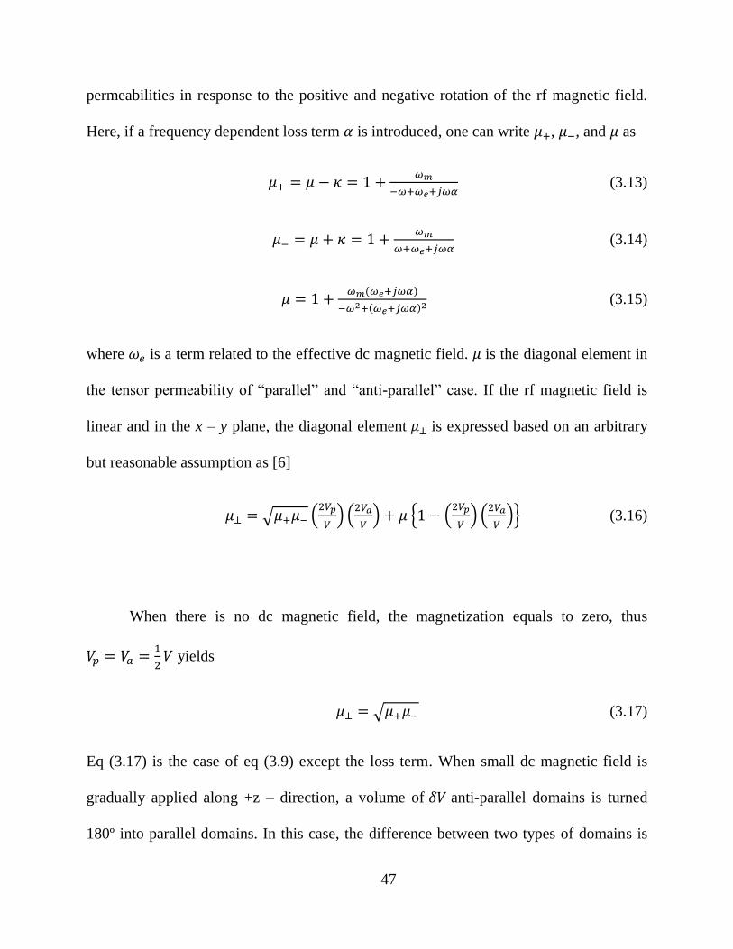
The magnetic permeability spectrum under varied magnetic bias is plotted in Fig.
4.3. When there is no magnetic bias, the initial permeability is 11, the value is then
dropped to a very low value close to zero at higher frequency, and at last, being close to
unity. When magnetic field is applied, the shape of the dispersion is quite different from
that under zero magnetic bias. Negative permeability region is observed, which has also
been shown in previous work from Tsutaoka, et al. [9]. Two peaks were observed which

62
was due to the existence of multi-modes associated with the large thickness of the YIG
slab. This is also shown in the FMR measurement. (Fig. 4.5)
The initial permeability is reduced under stronger in-plane bias magnetic field. At
the same time, the negative part of the real relative permeability is moved forward to
higher frequencies when the external magnetic field is increased. We can conclude that
when the bias magnetic field was larger than 800 Oe, the permeability was always
positive in frequency range of 0 – 4 GHz. In the later text, we will show that the YIG
substrate would not support propagation wave in the case when the permeability is
negative. Thus, if the designed central frequency is around 3.7 GHz, an in-plane magnetic
field of over 800 Oe should be applied to make sure the YIG substrate can always operate
in the positive permeability spectra region.
63
(a)
(b)
64
Fig. 4.3 Measured complex permeability of the ferrite (a) real part, and (b)
imaginary part.
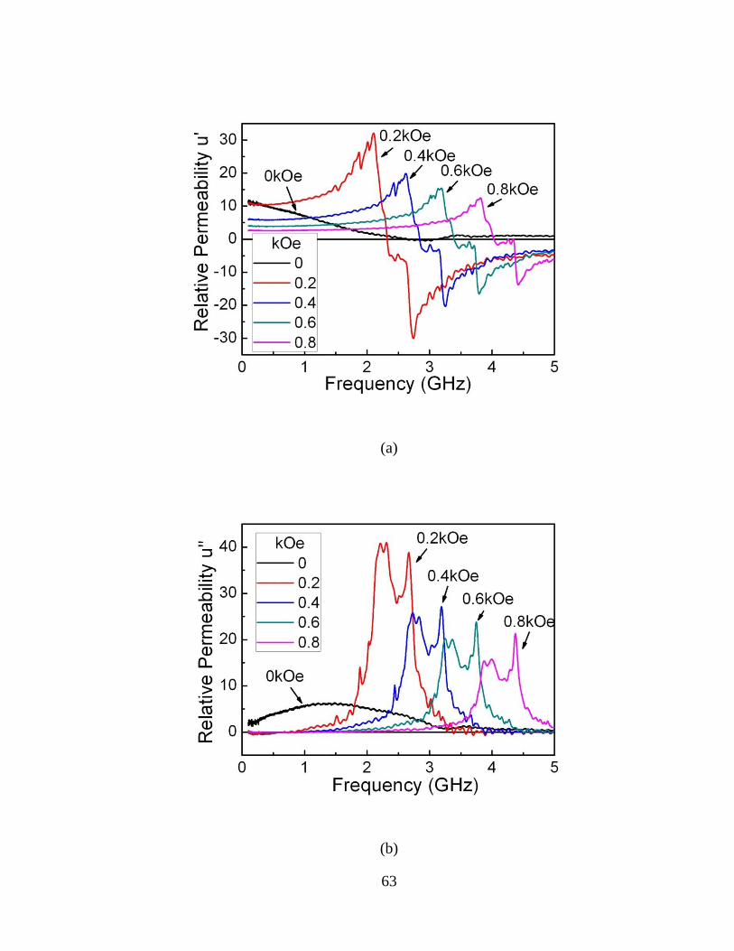
4.2.2. Magnetic hysteresis loop
The magnetic hysteresis loop is carried out by the Vibrating Sample
Magnetometer (VSM) with a saturation magnetization ( ) of 2100 Gauss, and a
coecivity of 1 Oe. (Fig. 4.4) The saturation magnetic field is 200 – 250 Oe for in plane,
and near 1500 Oe for out of plane.
Fig. 4.4 Measured normalized magnetic hysteresis loop of the doped YIG sample.

65
4.2.3. Ferromagnetic resonant frequency (FMR)
The narrow and FMR spectrum is carried out in our lab by using the system
described in [10]. RF source with different frequencies from 2.8 GHz to 3.7 GHz is
applied. Resonance peaks under various amplitude of magnetic field is observed, as
shown in Fig. 4.5. For a RF source with a certain frequency, e. g. 2.8 GHz, the material
show a main resonance peak under a magnetic field of 400 Oe and a second peak at
around 500 Oe. This indicates that when magnetic field of 400 Oe to 500 Oe is applied on
the material, the material will undergo an absorption band around this frequency range,
which will result in an unworkable bandgap in the microwave devices. However, the
FMR linewidth is measured less than 50 Oe implies that the material still exhibits a low
magnetic loss at off-FMR frequency region.

66
Fig. 4.5 Narrow band FMR measurement of the ferrite.
4.3. Resonator measurement verification
A single pole hairpin resonator at S-band is fabricated on the ferrite substrate in
order to verify the permeability measurement. First, a Cu seed layer is deposited onto the
ferrite substrate following by a 17 copper electroplating process. Next, the resonator
is patterned by standard photolithography. Finally, the device is put into 15% Nitride
Acid for wet etching.
The transmission coefficient under varied magnetic bias is carried out by our
network analyzer. The initial resonant frequency is at 3.72 GHz, though the device is to

67
be designed as a single resonator, the insertion loss exhibits a low value of 0.8 dB, which
show a great potential of implement a low loss ferrite based bandpass filter in this band.
When the applied magnetic field is increased to 800 Oe, the resonant frequency decreased
to 2.74 GHz with an insertion loss of 1.4 dB. The resonant frequency increased to 3.13
GHz when the magnetic field is increased to 1900 Oe, and the insertion loss decreased to
less than 0.2 dB. In this case, the frequency up shift is 390 MHz. The resonant frequency
up shifts more slowly at higher external magnetic field because the permeability change
of the YIG is getting smaller at higher bias fields. In addition, the frequency shift in this
band is not linear because of the non-linearity of permeability tuning by the external bias
field. A minimum insertion loss of 0.01 dB is obtained under 1300 Oe.
(a)

68
(b)
Fig. 4.6 Measured transmission coefficients (S21) and reflection ceofficients (S11).
When the magnetic field is applied between 200 Oe and 600 Oe, the device
exhibits an absorption band as predicted. The central resonance frequency is around 3.72
GHz, 3.75 GHz and 4.01 GHz, while the insertion loss increase to 7.33 dB, 8.65 dB, and
13.93 dB, respectively. The magnitude of the transmission and reflection are read from
Fig. 4.7, and calculated, as shown in Table 1. The small return loss and high insertion
loss indicates that almost 30% of the power has been reflected due to the impedance
mismatch while little power is transmitted through. The energy dissipation in the ferrite
increases from 51.86% to 67.81%. In other words, instead of band-passing behavior, the

69
wave transmission is almost prohibited between with an external magnetic field from 200
Oe to 600 Oe, the ferrite substrate will show a negative magnetic permeability from 2.3
to 4 GHz.
The relative permeability reading from Fig. 4.3 at each frequency is -9.4, -10.5,
and -12. According to the propagation factor , the phase constant is an attenuation
factor in this case, thus the wave will decay very quickly as the negative permeability
value decreased. This matches the measured permeability property of the substrate, where
shows negative region above 3.5 GHz when the external magnetic field is applied at 200
Oe 400 Oe, and 600 Oe.

70
Fig. 4.7 Measured s-parameters (S21 and S11) under 200 Oe, 400 Oe and 600 Oe.
Magnetic field
(Resonance
frequency)
200 Oe
(3.72GHz)
400 Oe
(3.75GHz)
600 Oe
(4.01GHz)
Insertion loss
(S21)
7.33dB
(18.49%)
8.65dB
(13.65%)
13.93dB
(4.07%)
Reflection
(S11)
5.28dB
(29.65%)
5.82dB
(26.18%)
5.51dB
(28.12%)
Power Absorbed 51.86% 60.17% 67.81%
Table 4.1 Loss calculation under 200 Oe, 400 Oe, and 600 Oe.

71
Fig. 4.8 Measured insertion loss under varied magnetic bias.
4.4. Conclusion
In this chapter, a method of measuring the complex permeability using a CPW and
a network analyzer is presented. The permeability spectra under varied magnetic field are
discussed. The measured permeability spectra show a negative region which prohibits the
wave propagation. Therefore, the energy of the RF source dissipated in the material, and
the attenuation depends on the magnitude of the negative value. In addition, a resonator is
fabricated on the ferrite substrate, the device showed an absorption band gap under a

72
magnetic field from 200 Oe to 600 Oe, which was in good agreement with the measured
permeability spectra.

73
4.5. Reference
1. D. Polder, “On the theory of ferromagnetic resonance,” Philos. Mag., vol. 40, p. 99,
January 1949.
2. P. Gelin, and K. Berthou-Pichavant, “New Consistent Model for Ferrite Permeability
Tensor with Arbitrary Magnetization State,” IEEE Trans. Microw. Theory Tech., vol.
45, no. 8, 1997.
3. G. T. Rado, “Theory of the microwave permeability tensor and Faraday effect in
nonsaturated ferromagnetic materials,” Phys. Rev., vol. 89, p. 529, 1953.
4. E. Schloemann, “Microwave behavior of partially magnetized ferrites,” J. Appl. Phys.,
vol. 41, pp. 204–214, Jan. 1970.
5. M. Igarashi, and Y. Naito, “Tensor Permeability of Partially Magnetized Ferrites,”
IEEE Trans. Magn., vol. MAG-13, no. 5, pp. 1664-1668, Sept. 1977.
6. J. Krupka, “Measurements of all complex permeability tensor components and the
effective line widths of microwave ferrites using dielectric ring resonators,” IEEE
Trans. Microwave Theory Tech., vol. 39, pp. 1148–1157, July 1991.
7. P. Queffelec, S. Mallegol, and M. Le Floc‟h, “Automatic Measurement of Complex
Tensorial Permeability of Magnetized Materials in a Wide Microwave Frequency
Range,” IEEE Trans. Microw. Theory Tech., vol. 50, no. 9, 2002.
8. Y. Ding, T. J. Klemmer, and T. M. Crawford, “A coplanar waveguide permeameter
for studying high-frequency properties of soft magnetic materils,” J. Appl. Phys., vol.
96, no. 5, p. 2969, Sept 2004.
9. T. Tsutaoka, T. Kasagi, K. Hatakeyama, and K. Fujimoto, “Negative Permeability
Spectra of Magnetic Materials,” Proceedings of iWAT2008, Chiba, Japan.
74
10. S. Beguhn, Z. Zhou, S. Rand, X. Yang, J. Lou and N. X. Sun, “A new highly sensitive
broadband ferromagnetic resonance measurement system with lock-in detection,” J.
Appl. Phys. Vol. 111, p. 07A503, 2012.

75
Chapter 5 : Multiferroic BPF on Partially Magnetized Ferrite
5.1. Motivation
Tunable bandpass filters are widely used in modern RF communication systems
with ever increasing demand on insertion loss, tunable range, bandwidth, linearity, size,
weight, power efficiency [1]. Ferrite filters, such as yttrium iron garnet (YIG) based
filters [2]-[7] and self-biased NiCo-ferrite based filters [8, 9] have been studied and
designed for different applications for years because of its low loss tangent, narrow
ferromagnetic resonance linewidth, wide operating frequency range and high stability.
One of the challenges with these types of ferrite filters or microwave ferrites based
devices, however, is that most of these microwave ferrites operate in their fully saturated
states with high tuning or bias fields up to several kilo-Oersteds in order to tune the
ferromagnetic resonant frequency to the frequency of interests due to their low saturation
and low anisotropy fields [4]-[6]. This leads to microwave magnetic devices that are
bulky and power consuming.
In this chapter, we start from the design of a magnetically tunable bandpass filter
on YIG substrate. A magnetically tunable bandpass filter under a low magnetic bias of
100 Oresteds shows a large tunability of over 6%. The power handling capability of the
device under varied magnetic bias is then discussed, and a high power handling capability
of 20 dBm is reported. Based on the concepts of partially magnetized ferrite‟s large

76
permeability tuning range under low magnetic biases, a dual magnetically and electrically
multiferroic tunable bandpass filter on a nickel ferrite substrate is then presented.
Compared to widely used YIG material, nickel ferrites exhibit a larger saturation
magnetostriction value which react more rapidly to the mechanical force induced by
piezoelectric phase.
5.2. Introduction to multiferroic tunable bandpass filters
Multiferroic composite materials consisting both a magnetic phase and a
ferroelectric phase are of great current interests, which offer the possibility of
magnetoelectric (ME) coupling, and have led to many novel multiferroic devices [4]-[6].
Compared to conventional tunable microwave magnetic devices that are tuned by
magnetic field [3, 7], these dual H- and E-field tunable microwave multiferroic devices
are much more energy efficient, less noisy, compact, and light-weight. However, these E-
field tunable multiferroic devices typically show very limited tunable frequency range
due to their limited effective E-field induced effective magnetic fields, which are
typically in the range of 5~50 Oe in epoxy bonded ferrite/ferroelectric heterostructures.
Most recently, Srinivasan, et al. [5] (Fig. 5.1) reported a magnetoelectric
microwave bandpass filter with a single crystal yttrium iron garnet–lead zirconate titanate
(YIG-PZT) bilayer to implement the communication of two microstrip antennas at

77
ferromagnetic resonant (FMR) frequency. By applying electric field across the thickness
of the piezoelectric sample, the mechanical deformation in piezoelectric phase results in
an anisotropy change in the magnetic phase, i. e., the YIG single crystal, which
corresponds to a FMR tuning. The metal electrodes on both sides of PZT plate produces
an electrical wall on top of the YIG single crystal, the device exhibits a reasonable
insertion loss of around 5 dB. Yang, et al. [4] (Fig. 5.2) also reported a better tunability at
L-band by using a similar concept yet they did not specify the insertion loss acquired
from the electric field tuning approach.
(a)

78
(b)
Fig. 5.1 Magnetoelectric microwave bandpass filter. (a) Device schematic and (b)
measured S21 parameter.

79
(a)
(b)
80
(c)
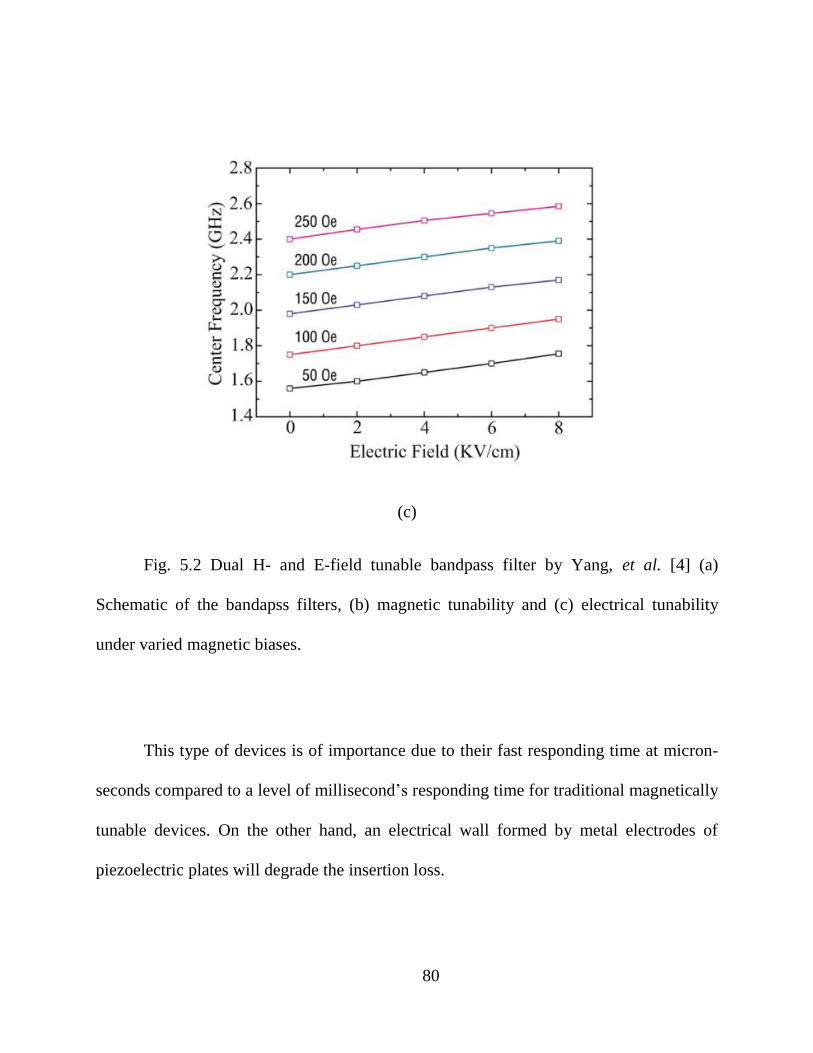
Fig. 5.2 Dual H- and E-field tunable bandpass filter by Yang, et al. [4] (a)
Schematic of the bandapss filters, (b) magnetic tunability and (c) electrical tunability
under varied magnetic biases.
This type of devices is of importance due to their fast responding time at micron-
seconds compared to a level of millisecond‟s responding time for traditional magnetically
tunable devices. On the other hand, an electrical wall formed by metal electrodes of
piezoelectric plates will degrade the insertion loss.

81
5.3. Magnetically tunable BPF based on partially magnetized ferrite
We present a magnetically tunable bandpass filter on partially magnetized YIG
substrate here as a start point. As stated in previous chapters, the permeability of partially
magnetized ferrites exhibits a very low value as well as a reasonable magnetic loss when
the ratio ⁄ is close to unity. Therefore, by carefully selecting the ferrite with a
proper saturation magnetization, bandpass filter with an initial central frequency at
different band can be implemented. At the same time, the material is also operated in a
low loss regime when the frequency is tuned within a limited range. At this point, the
need for low magnetic bias will lead the devices that are more power efficient.
5.3.1. Research efforts on BPF using partially magnetized ferrites
Partially magnetized ferrites have been used in tunable devices [10, 11] due to
their large permeability tunable range, low or zero bias field, and fast tuning speed at
micron-seconds. Analyses on the permeability tensor of partially magnetized ferrites
[12]-[16] indicated that these unsaturated ferrites have 0 <μr<1, which can be tuned by
changing its magnetization M between 0 ~Ms (the saturation magnetization) with a low
bias field. The permeability, at this point, exhibits a very low value as well as a
reasonable magnetic loss when the ratio ⁄ is close to unity. Therefore, by
carefully selecting the ferrite with a proper saturation magnetization, bandpass filter with
an initial central frequency at different band can be implemented. As a result, large
frequency tunability can be achieved in tunable RF/microwave ferrite devices with

82
partially magnetized ferrites with a low bias field, e.g. less than 150 Oe, since the
operating frequency √ ⁄ . At this point, the material is operated in a low loss
regime when the frequency is tuned within a limited range. The need for low magnetic
bias will lead the devices that are more power efficient.
Oates, et al. [11] (Fig. 5.3) reported a magnetically tunable superconducting
bandpass. The device was realized by printing a microstrip structure on top of a
polycrystalline YIG substrate and then tested under a low magnetic bias of less than 300
Oe. The tunability of the devices was 13% and the losses were well below 1 dB in
superconducting environments.
(a)

83
(b)
Fig. 5.3 Magnetically tunable superconducting bandpass filter (a) device
schematic and (b) S21 parameters.
5.3.2. Device construction
The device was constructed by following the same design consideration, but was
implemented with a more compact size in order to set the initial resonant frequency at C-
band to fulfill the requirement of the operating frequency range with respect to the
selected ferrite material. The dimension of the device is 5mm × 7mm with a thickness of
0.3mm. (Fig. 5.4) The ferrite substrate is chosen from the commercial product pure
polycrystalline YIG from Trans-Tech Inc (G-113). The saturation magnetization Ms is
1816 Gauss with a coercivity of 1.5 Oe. The YIG ceramic slab has a dielectric constant of

84
ε‟ = 14.59, an electric loss tangent tanδ=0.00004, and a linewidth of less than 24 Oe. The
structure of the bandpass filter is a compact, low loss single pole hairpin design
consisting of a “U” shaped resonator capacitively coupled to the input and output port.
The strip-lines were constructed by standard photolithography with 10-μm thick copper.
A uniform magnetic field from 0 to 100 Oe was applied parallel to the feed line. In this
case, the ferrite substrate is operated in a unsaturated state.
(a)

85
(b)
Fig. 5.4 (a) Geometry of the bandpass filter on YIG substrate and (b) fabricated
device.
5.3.3. Simulations and experimental verification
Unlike traditional simulation of magnetic bias excited spin waves inside the
magnetic materials, when the magnetic material is used as a substrate in a partially
magnetized state, it is hard to simulate the magnetic properties of the material under
varied magnetic bias. The HFSS only simulate the magnetic material in saturated states.
Therefore, the calculation of magnetic properties of the material is presented as a first
step of the simulation.

86
Following the theory of partially magnetized ferrites discussed in chapter 3, the
calculated complex permeability in demagnetized state is
according to eq (3.19). By knowing the permittivity, the electric loss and the
complex permeability value, one can predict the performance of the proposed bandpass
filter by insert the values into the material spec boxes. On the other hand, the
permeability can also be derived from the equation by knowing the instantaneous
magnetization, the magnitude of bias field and the resonant frequency of the bandpass
filter.
The under varied magnetic biases are calculated from such approach. (Fig. 5.5)
The calculated values correspond to a magnetic field sweep from 0 Oe to 100 Oe with a
step of 10 Oe in measurement. The simulation is implemented by setting the substrate
permeability value from 0.7 to 0.85 with a step size of 0.03. (Fig. 5.6)

87
Fig. 5.5 Calculated real part of complex permeability under varied magnetic biases
in partially magnetized states.
The insertion loss and position of initial central frequency in simulation, at zero
magnetic bias, is in agreement with the measurements indicates that the calculations
stand in this model. (Fig. 5.7)
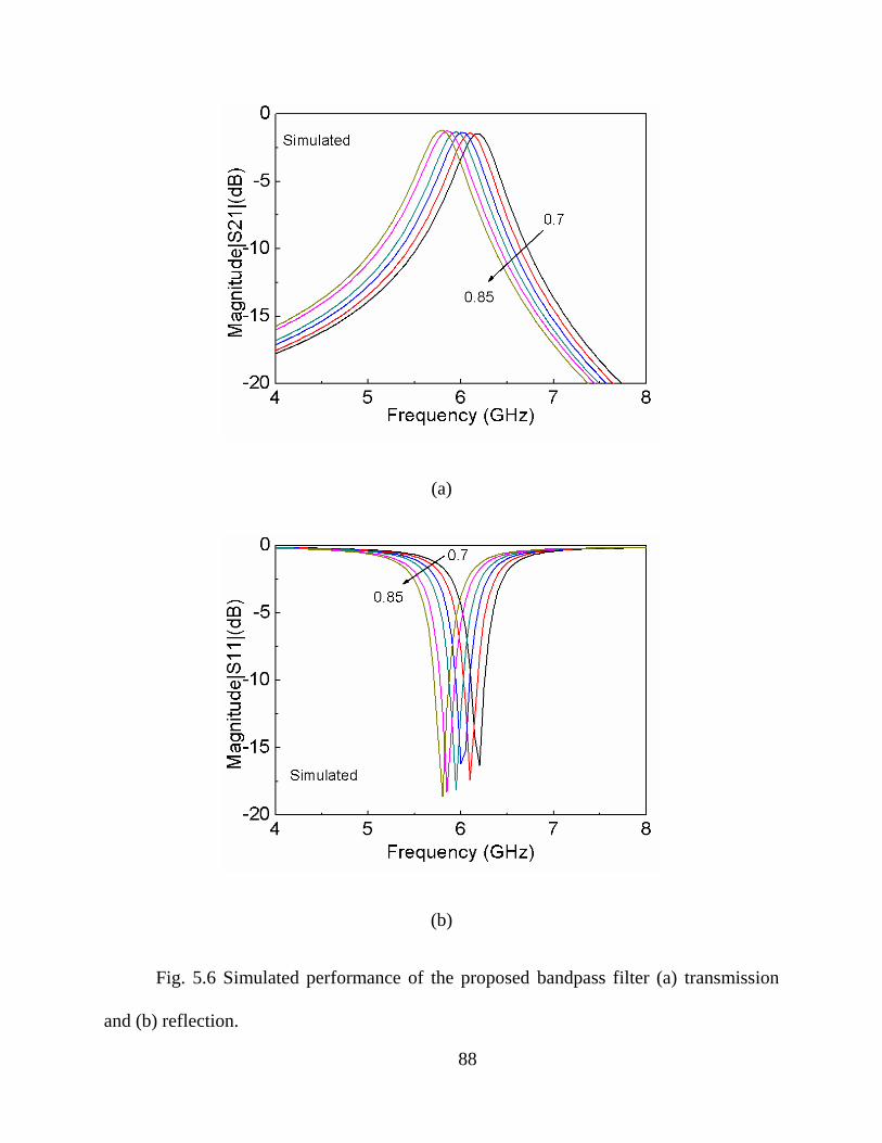
88
(a)
(b)
Fig. 5.6 Simulated performance of the proposed bandpass filter (a) transmission
and (b) reflection.

89
For non-zero cases, there may exist a difference between simulations and
measurements/calculations. For instance, at 100 Oe magnetic bias, the calculation gives a
permeability of 0.87 (Fig. 5.5) and 0.85 from the simulation. (Fig. 5.6) An error of two
percent is obtained.
(a)

90
(b)
Fig. 5.7 A comparison between simulation and measurement at zero magnetic bias.
The initial central frequency without a magnetizing field is 6.17 GHz with an
insertion loss of 1.1 dB. (Fig. 5.8) The 3-dB bandwidth is about 810 MHz. The bandpass
filter shows a large frequency shift of 290 MHz when the magnetizing field is increased
to 60 Oe. At this point, the central frequency is decreased to 5.88 GHz with a constant
insertion loss of 1.1 dB. The lowest central frequency occurs at 5.79 GHz under a
magnetic field of 100 Oe with a reasonable insertion loss of about 1.25 dB. The 3-dB
bandwidth is mainly determined by the hairpin structure. Narrower bandwidth can be
obtained by creating a multi-pole model. The bandwidth remains almost the same when

91
the YIG substrate transits from unsaturated to saturated states [2]. Compared to the
frequency shift when the bias magnetic field is less than 60 Oe, it shows a smaller shift of
80 MHz. This is due to the low variation of permeability under higher magnetic field
beyond 60 Oe [13].
The increase of the insertion loss at lower frequency indicates that with the
increase of magnetic field, the operating frequency is approaching the “low-field loss”
region of YIG material. The low bias field induced FMR absorption region in this case is
at about 1.2 GHz and will not contribute to the insertion loss [17] for this design.
(a)

92
(b)
Fig. 5.8 Measured (a) transmission (b) reflection coefficients under different
magnetizing fields. The measured central frequency shifted downward from 6.17 GHz to
5.79 GHz.
When strong bias field around 1 kOe is applied, the material is saturated. The
permeability spectrum exhibits a negative region which overlaps with the operation band
of the bandpass filter [2]. The electromagnetic waves quickly decay in the substrate and
will result in a high insertion loss over 10 dB. During the measurement, the return losses
were more than 18 dB indicating a good impedance match.

93
The central frequency simulation and measurement when the bias magnetic field is
varied from -100 Oe to 100 Oe is plotted. (Fig. 5.9) The simulated frequency under
varied bias magnetic field shows reasonable fit to the measured result. The difference is
induced by the error from the estimation of permeability by [8]. Small difference at low
permeability value (μr<1) will result in relatively large change in frequency domain. The
central frequency shows hysteresis behavior to the magnetic field due to the magnetic
hysteresis of the ferrite. This indicates that the magnetization has important effect to the
central frequency.
Fig. 5.9 Central frequency of the tunable bandpass filter under magnetic field from
-100 Oe to 100 Oe. The measurement (simulation) consists of a forward and a backward
loop. The central frequency exhibited a 0.3% shift at zero bias field due to the hysteresis.

94
Green and Sandy [15] measured the magnetization and magnetic loss of YIG
material at varied temperature from 23ºC to 200ºC. The saturation magnetization will
decrease with the increase of temperature. This will compress the tunability of the
bandpass filter since the frequency is directly related to the variation of magnetization. In
real applications, an additional packaging technique, e.g. heat sinks may be applied to
dissipate the heat effectively.
To summarize, the bandpass filter exhibits a large frequency tunability of 380
MHz (6.1%), a low insertion loss at the level of 1 dB and a good impedance match. By
varying the length of the hairpin resonator, initial central frequency at different location
can be obtained. However, for different initial central frequency, the permeability
operating range and the loss of the material varies from on to another depending on the
distance between the ratio ⁄ and unity. A simulation is given (table 5.1) that
depicts the trade-off between these factors. Higher permeability tuning range is obtained
and will result in higher frequency tunability. In the meantime, more loss will be
introduced from the magnetic loss of the YIG material.

95
Hairpin
length
(mm)
fc (GHz) under
zero Oe
under
100 Oe
Tunability
(MHz)
Insertion
loss (dB)
4.35 5.9 0.86 0.67-
j0.0063 0.83 450(7.6%) 1.6
4.1 6.17 0.82 0.71-
j0.0053 0.85 380(6.1%)
1.1
measured
1.44
simulated
3.8 6.44 0.79 0.74-
j0.0045 0.88 290(4.5%) 1.2
Table 5.1 Comparison of tunability and insertion loss in different designs.
From table 5.1, it is seen that different from traditional ferrite FMR based design,
the initial central frequency is mainly set by the geometry of the microstrip structure.
Therefore, different microstrip geometry can be employed for specific applications. The
frequency tunability is larger when the designed resonant frequency is more closed to
, and the permeability is operated in a wider range. On the other hand, the material
loss will increase to deteriorate the insertion loss. In addition, once the geometry is
printed on to the ferrite substrate, the device can only work within a very limited
frequency band. However, the exchange of large tunability and low tuning field is still
attractive for ferrite devices.
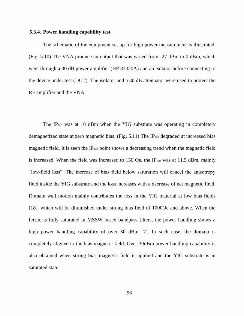
96
5.3.4. Power handling capability test
The schematic of the equipment set up for high power measurement is illustrated.
(Fig. 5.10) The VNA produce an output that was varied from -27 dBm to 0 dBm, which
went through a 30 dB power amplifier (HP 83020A) and an isolator before connecting to
the device under test (DUT). The isolator and a 30 dB attenuator were used to protect the
RF amplifier and the VNA.
The IP1dB was at 18 dBm when the YIG substrate was operating in completely
demagnetized state at zero magnetic bias. (Fig. 5.11) The IP1dB degraded at increased bias
magnetic field. It is seen the IP1dB point shows a decreasing trend when the magnetic field
is increased. When the field was increased to 150 Oe, the IP1dB was at 11.5 dBm, mainly
“low-field loss”. The increase of bias field below saturation will cancel the anisotropy
field inside the YIG substrate and the loss increases with a decrease of net magnetic field.
Domain wall motion mainly contributes the loss in the YIG material at low bias fields
[18], which will be diminished under strong bias field of 1000Oe and above. When the
ferrite is fully saturated in MSSW based bandpass filters, the power handling shows a
high power handling capability of over 30 dBm [7]. In such case, the domain is
completely aligned to the bias magnetic field. Over 30dBm power handling capability is
also obtained when strong bias magnetic field is applied and the YIG substrate is in
saturated state.
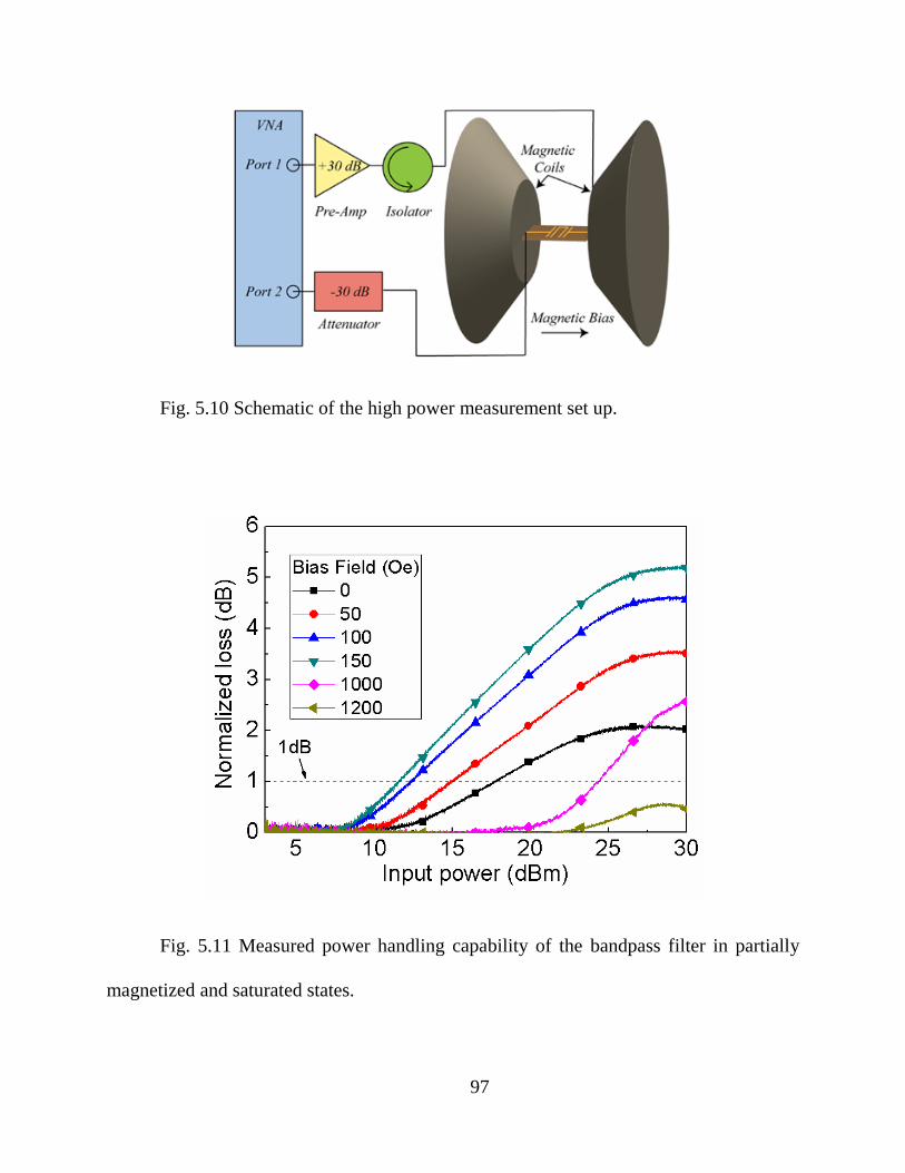
97
Fig. 5.10 Schematic of the high power measurement set up.
Fig. 5.11 Measured power handling capability of the bandpass filter in partially
magnetized and saturated states.
98
5.3.5. Summary of magnetically tunable BPF
The concept of tunable banspass filters based on partially magnetized ferrite are of
importance. The experiments have proved that although the magnetic loss of the ferrite in
partially magnetized state is claimed to be large and is not suitable to microwave devices,
the results still show an encouraging aspect in achieving both a large frequency tunability
and a low insertion loss with a very low magnetic bias. The need for low tuning magnetic
fields in the range of <100Oe for partially magnetized ferrites provides a unique
opportunity for dual H- and E-field tunable RF/microwave multiferroic devices, since the
low tuning magnetic field can be provided by the effective magnetic field induced by E-
field.
5.4. Multiferroic tunable bandpass filters
In this section, a three-pole hairpin tunable bandpass filters designs using partially
magnetized nickel ferrite substrate at Ku-band is presented. The unsaturated ferrite
substrate operated at a low permeability range from 0.56 to 0.7 under magnetic fields
from 0 to 150 Oe. In addition, multiferroic bandpass filters with ferrite/PMN-PT (lead
manganese niobate-lead titanate) structure are demonstrated. The bandpass filters have
electrically tunability of 270MHz (2.1%) with an electric field of 9kV/cm under a low
bias magnetic field of 100 Oe.

99
5.4.1. Bandpass filter on Nickel ferrite substrate
In this experiment, polycrystalline Ni-ferrite (NiFe2O4) from Trans Tech Inc.
commercial products (TT86-6000) is chosen as the substrate. Properties of the material
are listed in Table 5.2. The wider linewidth and slightly larger loss tangent of the nickel
ferrite results in more loss in microwave devices; however, the larger magnetostriction
compared to YIG materials leads to more electrical tunability in multiferroic applications.
In-plane magnetic hysteresis loops are measured with vibrating sample
magnetometer (VSM). (Fig. 5.12) The nickel ferrite with a saturation magnetic field of
about 300 Oe, is harder than the previously discussed YIG material. But similar as YIG,
the magnetization change of the materials also becomes less sensitive to magnetic field
when the ratio M/Ms is greater than 0.6, which result in slower permeability change
according to eq (3.19), corresponding to a bias magnetic field of 150 Oe.
12.17 0.0002 4750 Gauss 149 Oe ~25ppm
Table 5.2 Properties of nickel ferrite.

100
Fig. 5.12 Magnetic hysteresis loop of TT86-6000 nickel ferrite.
To meet the prerequisite of a partially magnetized device using nickel ferrite with
high saturation magnetization of 4750 Gauss, a tunable bandpass filter using partially
magnetized nickel ferrite at Ku-band is demonstrated. The dimension of the device is 6
mm 3.5 mm with a ferrite thickness of 0.25 mm. (Fig. 13) The structure is a three-pole
hairpin design [19] in order to obtain a narrower bandwidth. The device was constructed
by using standard photolithography technique with 5 um thick copper. The device was
then attached to a fixture with two SMA connectors for measurement. A bias magnetic
field from 0 to 150 Oe was applied parallel to the feeding line.

101
Fig. 5.13 Geometry of the bandpass filter. W=2.3mm, S1=1.3mm, S2=0.25mm,
S3=0.2mm, S4=0.55mm.
The initial resonant frequency of the bandpass filter is at 14.16 GHz with a 3 dB
bandwidth of 690 MHz (4.8%). The insertion loss is 5.5 dB and the return loss is 15 dB
due to high loss of the Ni-ferrite material. The central frequency is decreased to 14 GHz
with an insertion loss of 5.2 dB under a 50 Oe field. When the bias magnetic field is
increased to 100 Oe and 150 Oe, the frequency is decreased to 13.72 GHz and 13.35 GHz,
and the insertion loss is 5.5 dB and 6.1 dB, respectively. The 3 dB bandwidth is increased
to 950 MHz under 150 Oe and the bandpass behavior deteriorates. The resonant
frequency, in this case, is close to the “low-field loss” region and the quality factor of the
material is decreased. The return losses of the bandpass filter are greater than 15 dB and
the rejection band are more than 25 dB. The return loss exhibits high value below 12
GHz due to the high magnetic loss of the material at this frequency range.

102
(a)
(b)
Fig. 5.14 Measured (a) transmission and (b) reflection coefficients under different
magnetizing fields.

103
In order to obtain a large electrically tunability, bandpass filter with multiferroic
heterostructures was fabricated at 13.8 GHz. At lower frequency, the material exhibits a
higher permeability tuning range. The calculated permeability in demagnetized state is
μdemag= 0.51-j0.015. More energy dissipates in the materials in change of a higher
tunability. The frequency tuning range is from 13.8 GHz to 12.89 GHz under a magnetic
bias up to 150 Oe. (Fig. 5.15) The insertion loss of this device is around 14 dB (Fig. 5.18)
at this point. However, from previous experiments on nickel ferrite device, we had
demonstrated that the insertion loss is able to be compressed within 5 to 6 dB at Ku-band.
A fabrication improvement will lead to less insertion loss which is more suitable for
applications.
Fig. 5.15 A frequency distribution versus magnetic bias at a lower frequency.

104
5.4.2. Ni-ferrite/PMN-PT Multiferroic heterostructure
The multiferroic heterostructures was formed by epoxy bonding a 0.5 mm thick
ferroelectric PMN-PT (lead manganese niobate-lead titanate) single crystal, with d31
along x-axis, onto the back side of the device. (Fig. 5.16) The structure produces a strong
mechanical coupling and allows voltage tuning of the band pass filter. The glue
electrically isolated the device ground plane and the PMN-PT so that the piezoelectric
only has mechanical contribution to the filter. The effective magnetic field leads to an in-
plane anisotropy change inside the ferrite substrate which refers to a high permeability
tuning.
(a)

105
(b)
Fig. 5.16 (a) Diagram showing the device with ferrite/PMN-PT multiferroic
heterostructure, and (b) fabricated device.
Compared to the widely used PZT ceramics used in many multiferroic devices, the
PMN-PT single crystals with a d31 of -1800pC/N and a d32 of 900pC/N, not only have a
much larger piezoelectric coefficients, but also show an in-plane anisotropic piezoelectric
behavior that is critical for achieving large E-field tunability [20].
The nickel ferrite polycrytaline used here has a saturation magnetostriction λs ~ -
33ppm. Idealy, assuming the mechanical coupling between the ferroelectric phase and
magnetic phase is lossless, the effective in-plane magnetic field of the Ni-ferrite/PMN-PT
bilayer induced by stress can be obtained from inverse magnetoelastic relation (cgs):
𝑌 (5.1)

106
where λ is the ME coefficient. Y is the Young‟s modulus of bulk nickel spinel (
dyne/cm2), E is the electric field applied on the PMN-PT/ferrite bilayer, and deff is
the effective piezoelectric coefficient of the PMT-PT single crystal is given by
𝜈 3 3
𝜈
𝜈 3 3
𝜈
3 3
𝜈 (5.2)
where ν is the poisson‟s ratio of NiFe2O4 (~0.32). When an electric field from -1 kV/cm
to 9 kV/cm is applied, (2) gives a calculated ΔHeff change of up to 30 Oe in either x or y
dirction.
5.4.3. Measurement verification
An electric field from 1 to 9 kV/cm is applied along the thickness or [011]
direction of the PMT-PT slab. A magnetic bias with three different amplitudes, 0 Oe, 75
Oe and 100 Oe, along the y-axis are investigated, which corresponds to the three
observation points in Fig. 5.15. The lowest frequency occurs at 13.05 GHz under an
electric field of -1 kV/cm under a bias field of 100 Oe. The central frequency is increased
to 13.20 GHz and 13.32 GHz when the applied electric field is 5 kV/cm and 9 kV/cm. An
electrically tunability of 270 MHz (2.1%) is obtained under a bias field of 100 Oe and the
central frequencies show a good linearity to the applied electric field.. By using the same
measurement technique, tunability of the central frequencies under the magnetic bias of
75 Oe and 0 Oe are obtained as 160 MHz (1.2%) and 135 MHz (0.9%), as shown in Fig.
5. 17. This is due to the lower tuning rate of the device with respect to the magnetic field
107
under 75 Oe and 0 Oe compared to that under 100 Oe. In addition, the ME coefficient
increase of the nickel ferrite under stronger bias magnetic field contributes to the increase
of ΔHeff and change of anisotropy which is critical to the magnetization of the ferrite. On
the other hand, glue bonding induced clamping effect will reduce the substrate bending
and result in lower effectvie magnetic field comapres to the calcuation.
The observed frequency tunability, with no bias field, exhibits a opposite tuning
trend compared to the case of 75 Oe and 100 Oe. This is due to the PMN-PT induced
change of in-plane anisotropy under varied electric fields [20]. When bias field along y-
axis is applied, the monotonic change in anisotropy results in the unidirectional shift of
the central frequency. The tuning rate is reduced when the applied electric field was
further increased due to the saturation of the piezoelectric strain at higher E-fields.

108
Fig. 5.17 Measured E-field tunable operating frequency range of the bandpass
filter under different magnetic bias fields, showing the dual E- and H-field tunability.
Fig. 5.18 S21 curves of the multiferroic device under 100 Oe magnetic bias.
109
A more complete measurement on the central frequency of the bandpass filter as a
function of applied electric fields is depicted. (Fig. 5.19) The measurement consists of a
forward loop (-9 kV/cm to 9 kV/cm) and a backward loop (9 kV/cm to -9 kV/cm). A
clear hysteresis loop can be observed with a “butterfly” shape. This “butterfly” central
frequency resembles the widely observed piezoelectric strain vs. electric field curves for
piezoelectric materials [20] and matches the ferroelectric P-E hysteresis loop of PMN-PT
single crystal as well. Therefore, as previously discussed, the central frequency hysteresis
confirms that the device realized the control of the magnetization of nickel ferrite with
piezoelectrics induced strains which show great potential for electrcially tunable
multiferroic devices.

110
Fig. 5.19 Central resonant frequency show “butterfly” behavior.
5.5. Conclusion
In this chapter, starting from the state of art of the multiferroic tunable bandpass
filters, a question has been raised: how to implement a tunable bandpass filter that has a
larger electrically tunability, low insertion loss and power efficient. An engineering
approach that combining both the concepts of partially magnetized ferrite and
magnetoelectric coupling is proposed. The idea is to use the multiferroic heterostructure
in control of anisotropy of the ferrite to tune the permeability in its rapid tuning region.
111
Two experiments are presented:
1) A planar compact bandpass filter at C-band on a partially magnetized YIG
substrate was demonstrated with a large tunability of 380 MHz (6.1%), a
low insertion loss of 1.1 dB to 1.25 dB under low magnetic field of 0 to 100
Oe. The bandpass filter on unsaturated ferrite substrate also showed IP1dB up
to 18 dBm and over 30 dBm in saturated state.
2) A Ku-band multiferroic tunable bandpass filter on nikel spinel with an
electrcially tunability of 270 MHz (2.1%) is presented. The experiment
discussed the usage of the spinel‟s high magnetostriction in microwave
devices. The frequency tunability is closely related to the ferrite
permeability operating region. In addition, the measured central frequency
under varied electric field showed a “butterfly” behavior due to the
magnetic hysteresis of the nickel ferrite substrate in response to the PMN-
PT single crystal.

112
5.6. References
1. J. S. Hong and M. J. Lancaster, Microstrip Filters for RF/Microstrip Applications.
New York: J. Wiley & Sons, 2001.
2. X. Yang, J. Wu, S. Beguhn, Z.Y. Zhou, J. Lou and N. X. Sun, "Novel C-Band
Tunable Bandpass Filter with Low Bias Magnetic Fields Using Partially Magnetized
Ferrites," Microwave Symposium Digest, IEEE MTT-S International, pp. 1-3, Jun.
2012.
3. X. Yang, J. Wu, J. Lou, X. Xing, D.E. Oates, G.F. Dionne and N.X. Sun, “Compact
tunable bandpass filter on YIG substrate,” Electron. Lett., vol. 48, no. 17, pp. 1010-
1071, 2012.
4. G. M. Yang, et. al., “Dual H- and E-field Tunable Multiferroic Bandpass Filters with
Yttrium,” Microwave Symposium Digest, IEEE MTT-S International, pp. 1-4, Jun.
2011.
5. A. S. Tatarenko, V. Gheevarughese and G. Srinivasan, “Magnetoelectric microwave
bandpass filter,” Electronic Letters, vol. 42, no. 9, pp. 540-541, April 2006.
6. C. Pettiford, S. Dasgupta, J. Lou, S. D. Yoon, N. X. Sun, “Bias field effects on the
microwave frequency behavior of a PZT/YIG magnetoelectric bilayer,” IEEE Trans
Magn., vol 43, no. 7, pp. 3343-3345, July 2007.
7. J. Wu, X. Yang, S. Beguhn, J. Lou, and N.X. Sun, “Nonreciprocal Tunable Low-Loss
Bandpass Filters with Ultra-Wideband Isolation Based on Magnetostatic Surface
Wave,” IEEE Trans. Microw. Theory Tech, vol. 60, no. 12, pp. 3959-3968, Dec. 2012.
8. G. M. Yang, A. Shrabstein, X. Xing, O. Obi, S. Stoute, M. Liu, J. Lou, and N.X. Sun,
“Miniaturized Antennas and Planar Bandpass Filters With Self-Biased NiCo-Ferrite
Films,” IEEE Trans. Magn., vol. 45, no. 10, pp. 4191-4194, Oct. 2009.

113
9. G. M. Yang, O. Obi, G. Wen, and N. X. Sun, “Design of Tunable Bandpass Filters
With Ferrite Sandwich Materials by Using a Piezoelectric Transducer,” IEEE Trans.
Magn. vol. 47, no. 10, pp. 3732-3735, Oct. 2011.
10. G. F. Dionne and D. E. Oates, “Tunability of Microstrip Ferrite Resonator in the
Partially Magnetized State,” IEEE Trans. Magn., vol. 33, no. 5, pp. 3421-3423, Sept.
1997.
11. D. E. Oates and G. F. Dionne, “Magnetically Tunable Superconducting Resonators
and Filters,” IEEE Trans. App. Supercon., vol. 9, no. 2, pp. 4170-4175, June, 1999.
12. E. Schlomann, “Microwave Behavior of Partially Magnetized Ferrites,” J. Appl. Phys.,
vol. 41, pp.1350, Mar.1970.
13. J. J. Green and F. Sandy, “Microwave Characterization of Partially Magnetized
Ferrites,” IEEE Trans. Microw. Theory Tech, vol. MTT-22, no. 6, pp. 641-645,
Jun.1974.
14. M. Igarashi, and Y. Naito, “Tensor Permeability of Partially Magnetized Ferrites,”
IEEE Trans. Magn., vol. MAG-13, no. 5, pp. 1664-1668, Sept. 1977.
15. J. J. Green and F. Sandy, “A Catalog of Low Power Loss Parameters and High Power
Thresholds for Partially Magnetized Ferrites,” IEEE Trans. Microw. Theory Tech, vol.
MTT-22, no. 6, pp. 645-651, Jun.1974.
16. M. Igarashi, and Y. Naito, “Parallel Component μz of Partially Magnetized Microwave
Ferrites,” IEEE Trans. Microw. Theory Tech, vol MTT-29, no.6, pp. 568-571, June.
1981.
17. C. E. Patton, “Microwave Properties of Fine Grain Polycrystalline Yttrium Iron
Garnet,” J. Appl. Phys., vol. 41, pp.1355, 1970.
18. Arthur J. Baden Fuller, Ferrites at Microwave Frequencies, London: Peter Peregrinus,
1987.

114
19. E. G. Cristal, and S. Frankel, “Hairpin-Line and Hybrid Hairpin-Line/Half-Wave
Parallel-Coupled-Line Filters,” IEEE Trans. Microw. Theory Tech, vol. MTT-20, no.
11, pp. 719-728, Nov. 1972.
20. J. Lou, D. Reed, M. Liu, C. Pettiford, and Nian. X. Sun, “Novel Electrostatically
Tunable FeGaB/(Si)/PMN-PT Multiferroic Heterostructures for Microwave
Application,” Microwave Symposium Digest, IEEE MTT-S International, pp. 33-36,
Jun. 2009.
115
Chapter 6 : Voltage Tunable Multiferroic Phase Shifter
Phase shifters are important components in RF/microwave systems. They are
widely used in many RF/microwave modules and circuits such as phase discriminators,
beam forming networks, power dividers, linearization of power amplifiers, and phase
array antennas, etc. Tunable phase shifters allow the application of a single device with
multiple functions. Among numerous phase shifters they are always required to be
tunable, compact, lightweight, low loss, fast responding time, and power efficient, etc.
In this chapter, we will present a compact voltage tunable multiferroic phase
shifter on yttrium iron garnet (YIG)/lead magnesium niobate lead titanate (PMN-PT)
heterostructure. The device exhibited a phase shift more than 115º under an electric field
of 11 kV/cm, and a reasonable low insertion loss of 3.7 dB compared to the state of art of
ferrite based phase shifters. The formation and design consideration of the device will
also be discussed. A comparison of E-field tunability between 1-layer PMN-PT structure
and 2-layer PMN-PT structure using bending mode is discussed. An over 20%
improvement on the phase shift over the proposed frequency range is reported. The
device combining with multiferroics and partially magnetized ferrite concepts is able to
operate with the absence of external bias magnetic field is more compact and power
efficient than traditional multiferroic devices.
116
6.1. Introduction to phase shifters
Phase shifters are used to change the transmission phase angle (phase of S21) of a
network. Ideal phase shifters provide low insertion loss, and equal amplitude (or loss) in
all phase states. While the loss of a phase shifter is often overcome using an amplifier
stage, the less loss, the less power that is needed to overcome it. Most phase shifters are
reciprocal networks, meaning that they work effectively on signals passing in either
direction. Phase shifters can be controlled electrically, magnetically or mechanically. The
major parameters which define the RF and microwave Phase Shifters are: frequency
range, bandwidth (BW), total phase variance (Δ ), insertion loss (IL), switching speed,
power handling (P), accuracy and resolution, input/output matching (VSWR) or return
loss (RL), harmonics level.
Most commonly used in electronically scanned antenna arrays the antenna beam
can be steered in the desired direction without physically repositioning the antenna by
applying a phase shifter to each antenna. When steering the beam, the phase of the
elements is adjusted so that individual signals line up at the desired beam-pointing angle
(theta).A total phase shift variation of 360º ( rad) is often needed to realize the phase
tuning of a single radiation element. The simplest way of controlling signal phase is to
systematically vary the cable lengths to the elements. Cables delay the signal and so shift
the phase. However, this does not allow the antenna to be dynamically steered. For this
reason, a tunable phase shifter is highly desired for modern radar systems.
117
6.1.1. State of art of tunable phase shifters
Different techniques and approaches have been employed in achieving phase shift
in RF/microwave components. Currently, most phased array antenna systems rely on
ferrite [1-3], MMIC [4], or MEMS [5-7] phase shifters. Moreover, new approaches such
as piezoelectric transducers (PET) [8, 9], field effect transistor (FET) switches [10], and
ferroelectric phase shifters [11] are drawing more attention to the researchers.
MEMS phase shifters have much faster response speeds (measure in
milliseconds), however their major drawback is that they have high losses at microwave
and millimeter-wave frequencies. Other disadvantages with MEMS phase shifters is that
they have limited power-handling capability (20 dBm) and they may need expensive
packaging to protect the movable MEMS bridges against the environment. MMIC phase
shifters are blazing fast, they can easily change state in tens of nanoseconds, but power
handling is limited to 10 milliwatts. They can also be very expensive, as they are
processed on gallium arsenide, not silicon. PIN diodes can also be used to make very
low-loss phase shifters, however they are mostly controlled by current. These limitations
prevent their applications in mission critical phased arrays, such as high power radars and
electronic warfare.

118
6.1.2. Application of ferrites in tunable phase shifters
Ferrite ceramics are used in tunable phase shifters as well as other RF/microwave
components for several decades due to the low loss, high power capability, high
resolution and reliability. Roome and Hair [12] reported a ferrite-dielectric phase shifter.
Though the device was only focused on the interaction between the wave propagation
and the ferrite without any tunability, many latter works on magnetic field tunable phase
shifters [13-15, 19, 20] were based on the theory. However, ferrite phase shifters are slow
to respond to control signals (often at milliseconds) and cannot be used in applications
where rapid beam scanning is required.
A desirable alternative is the latching waveguide ferrite phase shifter [1] that
operates at the remanent magnetization for the ferrite element and requires current pulses
for switching the magnetization state. Dionne and Oates [2] presented a microstrip phase
shifter with a similar concept but with a more compact planar profile. Though a very
large phase shifter over 1000º/dB was reported, the device was operated under a
superconducting environment. The ferrite in this type of device is operated before
saturation, by changing the magnetic flux of a closed loop within the path of ferrite, the
ferrite is then magnetized into any states. As previously discussed, a rapid change of
permeability will be obtained in this case. On the other hand, this type of devices is not
reciprocal and need to be reset in order to be tuned to another new state.
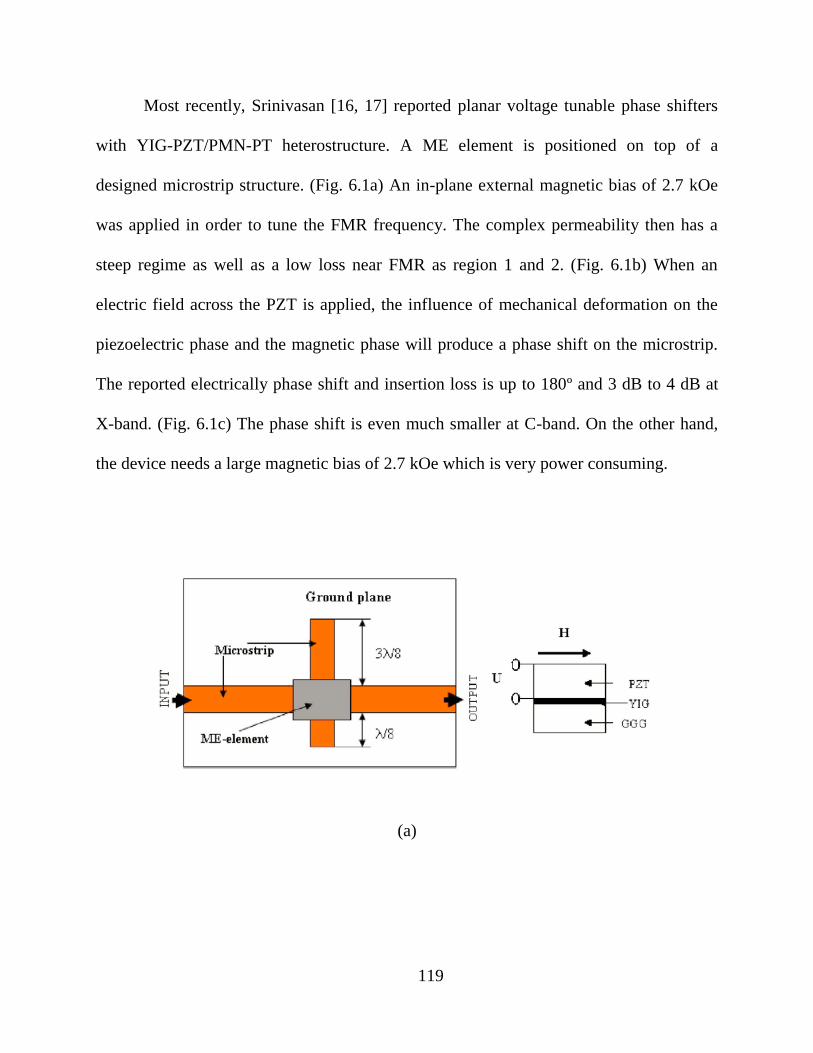
119
Most recently, Srinivasan [16, 17] reported planar voltage tunable phase shifters
with YIG-PZT/PMN-PT heterostructure. A ME element is positioned on top of a
designed microstrip structure. (Fig. 6.1a) An in-plane external magnetic bias of 2.7 kOe
was applied in order to tune the FMR frequency. The complex permeability then has a
steep regime as well as a low loss near FMR as region 1 and 2. (Fig. 6.1b) When an
electric field across the PZT is applied, the influence of mechanical deformation on the
piezoelectric phase and the magnetic phase will produce a phase shift on the microstrip.
The reported electrically phase shift and insertion loss is up to 180º and 3 dB to 4 dB at
X-band. (Fig. 6.1c) The phase shift is even much smaller at C-band. On the other hand,
the device needs a large magnetic bias of 2.7 kOe which is very power consuming.
(a)

120
(b)
(c)
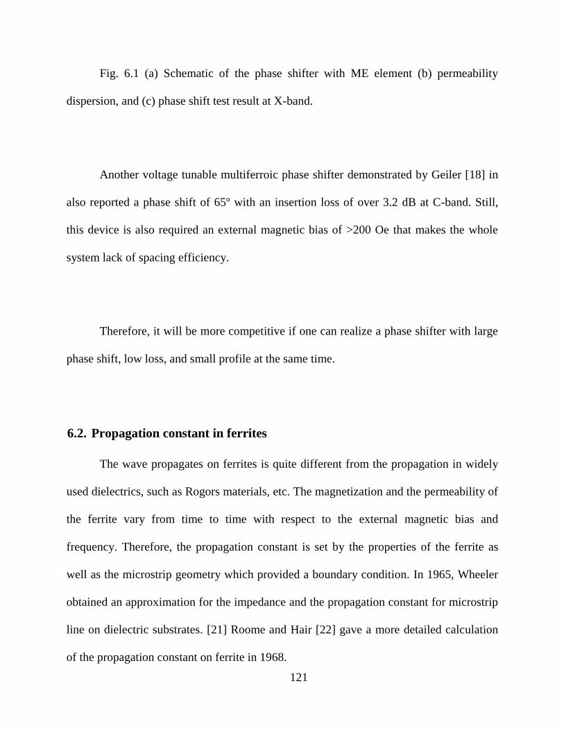
121
Fig. 6.1 (a) Schematic of the phase shifter with ME element (b) permeability
dispersion, and (c) phase shift test result at X-band.
Another voltage tunable multiferroic phase shifter demonstrated by Geiler [18] in
also reported a phase shift of 65º with an insertion loss of over 3.2 dB at C-band. Still,
this device is also required an external magnetic bias of >200 Oe that makes the whole
system lack of spacing efficiency.
Therefore, it will be more competitive if one can realize a phase shifter with large
phase shift, low loss, and small profile at the same time.
6.2. Propagation constant in ferrites
The wave propagates on ferrites is quite different from the propagation in widely
used dielectrics, such as Rogors materials, etc. The magnetization and the permeability of
the ferrite vary from time to time with respect to the external magnetic bias and
frequency. Therefore, the propagation constant is set by the properties of the ferrite as
well as the microstrip geometry which provided a boundary condition. In 1965, Wheeler
obtained an approximation for the impedance and the propagation constant for microstrip
line on dielectric substrates. [21] Roome and Hair [22] gave a more detailed calculation
of the propagation constant on ferrite in 1968.
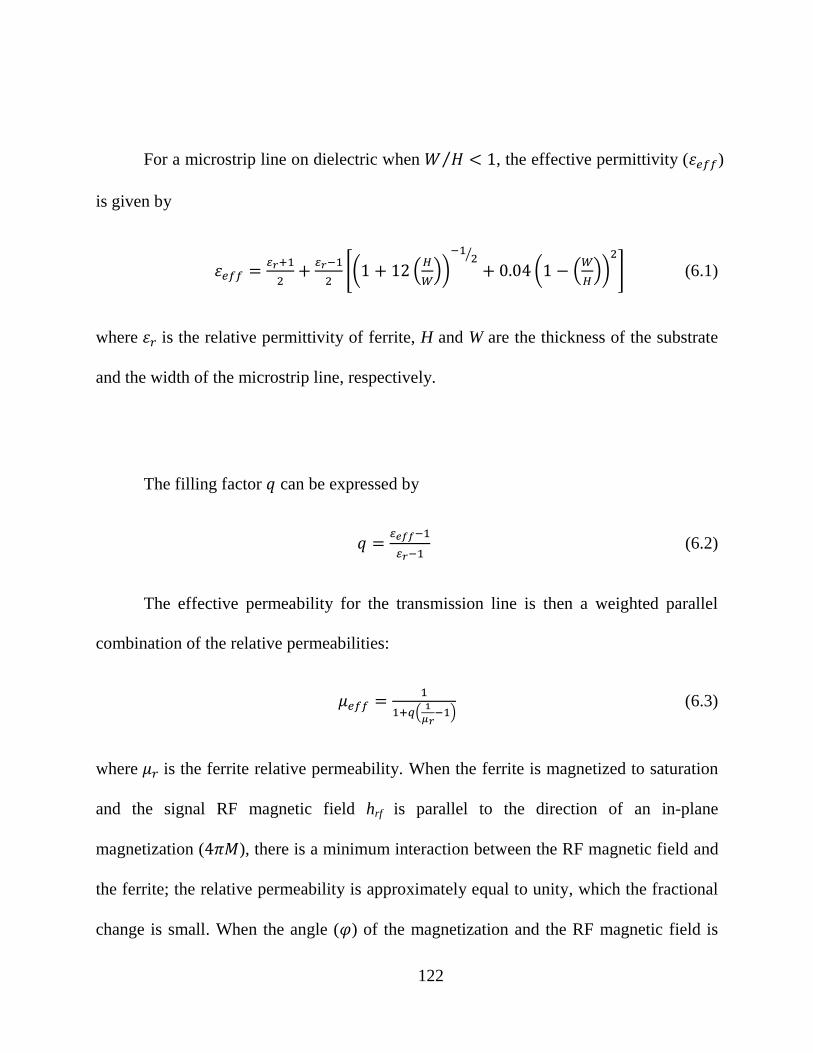
122
For a microstrip line on dielectric when ⁄ , the effective permittivity ( )
is given by
0( (
))
⁄
( (
))
1 (6.1)
where is the relative permittivity of ferrite, H and W are the thickness of the substrate
and the width of the microstrip line, respectively.
The filling factor can be expressed by
(6.2)
The effective permeability for the transmission line is then a weighted parallel
combination of the relative permeabilities:
(
)
(6.3)
where is the ferrite relative permeability. When the ferrite is magnetized to saturation
and the signal RF magnetic field hrf is parallel to the direction of an in-plane
magnetization ( ), there is a minimum interaction between the RF magnetic field and
the ferrite; the relative permeability is approximately equal to unity, which the fractional
change is small. When the angle ( ) of the magnetization and the RF magnetic field is

123
90º, there is a maximum interaction. (Fig. 6.2) An approximation of in the frequency
range ⁄ under small magnetic bias is given by [22]
(
)
(6.4)
where , is the ferrite magnetization, and is the gyromagnetic ratio
being 2.8 GHz/kOe.
Fig. 6.2 Wave propagation, signal RF magnetic field and magnetization
configuration.
When the magnetization is varied with small external magnetic bias H, if the
FMR frequency , the effective permeability in this case is given by [23]

124
, [ ( ) ]
- (6.5a)
|
| (
) (
) (6.5b)
where and are demagnetizing factors along y and z-axis, suppose the wave
propagates along z-axis. For a slab with y-axis perpendicular to the board face,
, . is the resonance linewith from spin-lattice relaxation damping.
By knowing these values, one can obtain the propagation constant in ferrite in
terms of frequency yields
( ) √ (6.6)
where and are magnetic and dielectric constant in free space, respectively. For a
microstrip with a fixed line width and substrate thickness, the only parameter can be
tuned by the external magnetic bias is the effective permeability . Therefore, the
phase shift of a microstrip ferrite phase shifter is approximately estimated by
( ) (6.7)
where is the effective length of the microstrip along the ferrite magnetization axis.

125
6.3. Device construction
In this section, a proposal of voltage tunable multiferroic phase shifters will be
presented. Different piezoelectric operating mode will also be discussed.
6.3.1. Meander line phase shifter with YIG/PMN-PT bilayer
A phase shifter on polycrystalline YIG substrate (TransTech–G113) was designed
and fabricated. (Fig. 6.3) The dimension of the device is 20 mm 10 mm with a
thickness of 0.3mm. The structure of the phase shifter is a compact quarter wavelength
meander line design with a length of about 100 mm.
The phase shifter was designed at C-band. The ferrite operating in this frequency
range exhibits a low permeability and a relatively low magnetic loss tangent as
previously discussed. Small tuning of the magnetic bias will result in high relative
variation of the. Therefore, large tunability in phase response is expected.

126
(a)
(b)
Fig. 6.3 (a) Geometry of meander line phase shifter and (b) fabricated device on
YIG substrate with PMN-PT bonding.

127
The fabricated phase shifter on YIG substrate is also shown in Fig. 6.3. The strip-
lines were constructed by electrode plating with 17 µm copper following by wet etching
techniques. The phase shifter was attached to a fixture with an SMA connector during
measurement. An in-plane uniform magnetic field was applied perpendicular to the feed
line (Fig. 6.3a) in order to obtain a magnetically tunable phase shifter on partially
magnetized substrate.
Next, a 0.5mm thick PMN-PT single crystal plate with an approximately equal
size was bonded onto the back side of the ferrite substrate using epoxy. (Fig. 6.3b) The
glue electrically isolated the ferrite and the PMN-PT plate so that the metal electrodes as
well as the applied voltage across the PMN-PT do not affect the electrical performance of
the phase shifter. Instead, a deformation of the piezoelectric will produce a mechanical
force which will be transferred to the ferrite phase through the ferrite-piezoelectric
bilayer.
6.3.2. Phase shifter with stack 2-layer PMN-PT/YIG structure
By knowing the relation between phase shift and the propagation constant from eq
(6.6), larger phase shift can be obtained by increasing the length of the microstrip.
Therefore, another structure is designed on an identical substrate with a three-stage

128
cascade double spiral microstrip structure. For each single element, the trace follows the
equation (Fig. 6.4a)
(6.7a)
(6.7b)
where θ is from 2π to 6π. The two spirals are then connected with an “S” shaped arc line.
The length of the cascade structure is calculated to be approximately 130 mm. By
increasing (decreasing) the spacing between the lines, the center of the operating
frequency band is decreased (increased).
The strip-lines were also constructed by electrode plating with 10 µm copper
following by wet etching techniques. Then, a 0.5mm thick, (011) cut and (001) poled
PMN-PT single crystal PMN-PT single crystal plate was bonded onto the back side of the
ferrite using epoxy with d31 along the x-axis. In order to strengthen the mechanical
deformation of the piezoelectric phase, another piece of PMN-PT single crystal with the
same size was bonded to the first PMN-PT plate to form a stacked 2-layer structure. (Fig.
6.4b) The second plate was also (011) cut and (001) poled. The d31 was also along the x-
axis. An opposite electric field was applied to the two PMN-PT plates for measurement at
this point.

129
(a)
(b)
Fig. 6.4 (a) Geometry of the phase shifter and layer demonstration, (b) fabricated
device with fixture.
130
6.4. Simulation
The transmission and reflection coefficients of the two designs are simulated with
HFSS V12. Since the ferrite model in HFSS are all in fully saturated case, similar to the
simulation techniques in the previous chapter, the permeability is set as a sweeping
parameter in order to obtain the coefficients in different states.
It is seen from Fig 6.5 and 6.6, for both designs, the insertion losses are less than 3
dB and the return losses are better than 10 dB. However, in real devices, the insertion loss
at this frequency range is expected to be higher than simulation due to the “low field loss”
of the ferrite material. Especially for the double spiral structure with a narrower
bandwidth, high insertion loss of the material and the cut-off region of the wave
propagation will add up to high loss at lower frequencies. However, by increasing the line
gaps one can lower the pass band central frequency to obtain higher phase shift and lower
loss.

131
(a)
(b)
Fig. 6.5 Simulated (a) transmission and (b) reflection coefficients of the meander
line ferrite phase shifter.

132
Fig. 6.6 Simulated transmission and reflection coefficients of double spiral phase
shifter.
6.5. Numerical results
The simulation on ferrite in HFSS when the ferrite is in partially magnetized state
is quite different from that in fully saturated state which is mostly used in spin wave
mode. The ferrite permeability spectrum is a function of frequency and can vary by over
80 percent in a very small frequency interval. In addition, the interaction between the
signal RF magnetic field and the magnetization is also need to be taken in to account.
Therefore, in this section, the numerical results of the meander line design (Fig. 6.3) is
brought up as the simulation result.

133
The YIG material used in this device exhibited a dielectric constant .
Thus, from Eq (6.1), (6.2), one can obtain the effective permittivity , and the
filling factor . The phase shift of the phase shifter can be obtained from Eq (6.5)
– (6.7) as in Fig. 6.7.
Fig. 6.7 Calculated phase shift of the meander line phase shifter.
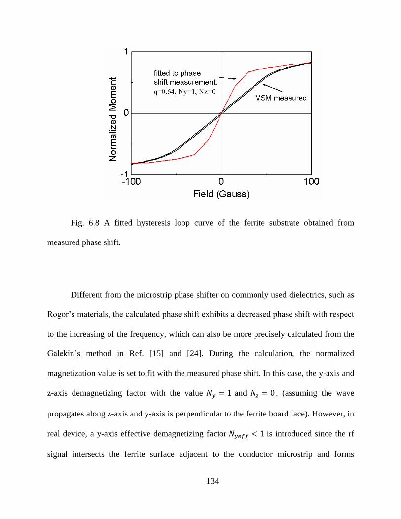
134
Fig. 6.8 A fitted hysteresis loop curve of the ferrite substrate obtained from
measured phase shift.
Different from the microstrip phase shifter on commonly used dielectrics, such as
Rogor‟s materials, the calculated phase shift exhibits a decreased phase shift with respect
to the increasing of the frequency, which can also be more precisely calculated from the
Galekin‟s method in Ref. [15] and [24]. During the calculation, the normalized
magnetization value is set to fit with the measured phase shift. In this case, the y-axis and
z-axis demagnetizing factor with the value and . (assuming the wave
propagates along z-axis and y-axis is perpendicular to the ferrite board face). However, in
real device, a y-axis effective demagnetizing factor is introduced since the rf
signal intersects the ferrite surface adjacent to the conductor microstrip and forms

135
magnetic poles. [23] This results in the difference between the fitted hysteresis loop and
the measured magnetic hysteresis loop of the ferrite substrate. (Fig. 6.8)
6.6. Measurement verification
6.6.1. Meander line phase shifter
Magnetically tunability:
Transmission and reflection coefficients measurements of the fabricated bandpass
filter were carried out by a network analyzer under various external magnetizing fields
from 0 to 100 Oe. (Fig. 6.9) The insertion loss is 3.6 dB under zero bias magnetic field
from 5.5 GHz to 7.5 GHz. When the bias field is increased to 100 Oe, the insertion loss is
increased to 5.1 dB. The insertion loss is induced mainly by the “low-field” loss. This is
due to the domain wall motion when the ferrite substrate operated in partially magnetized
state. Return losses are all better than 15 dB indicating a good impedance match during
the measurement. It is seen that the insertion loss is increased and the pass band behavior
is deteriorated, at lower frequency, when the applied magnetic field is increased. This is
due to the increasing of cut-off frequency of wave propagation in ferrite substrates under
higher magnetic field.
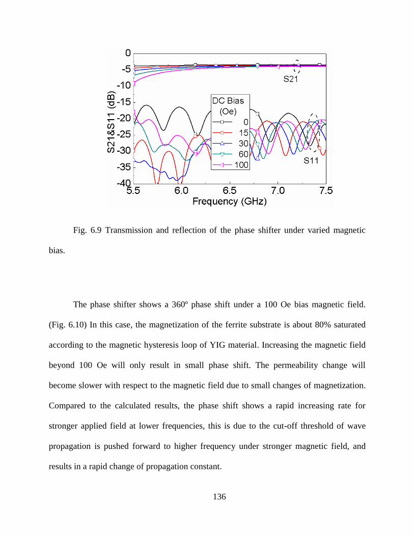
136
Fig. 6.9 Transmission and reflection of the phase shifter under varied magnetic
bias.
The phase shifter shows a 360º phase shift under a 100 Oe bias magnetic field.
(Fig. 6.10) In this case, the magnetization of the ferrite substrate is about 80% saturated
according to the magnetic hysteresis loop of YIG material. Increasing the magnetic field
beyond 100 Oe will only result in small phase shift. The permeability change will
become slower with respect to the magnetic field due to small changes of magnetization.
Compared to the calculated results, the phase shift shows a rapid increasing rate for
stronger applied field at lower frequencies, this is due to the cut-off threshold of wave
propagation is pushed forward to higher frequency under stronger magnetic field, and
results in a rapid change of propagation constant.

137
Fig. 6.10 Measured (colored lines) and calculated (colored scatters) phase shift
under varied magnetic bias.
It is seen the device exhibits an over 105º phase shifter under 15 Oe bias field, this
gives an opportunity for realizing multiferroic device controlled by electric field since
low effective magnetic bias produced by piezoelectric-ferrite heterostructure is suitable
for the low bias field requirement in this device.
The measured differential phase shift per insertion loss in degree/decibel under
varied external magnetic field is plotted in Fig. 6.11. A 68 degree/dB loss is measured at
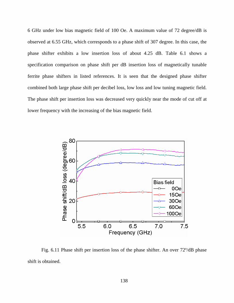
138
6 GHz under low bias magnetic field of 100 Oe. A maximum value of 72 degree/dB is
observed at 6.55 GHz, which corresponds to a phase shift of 307 degree. In this case, the
phase shifter exhibits a low insertion loss of about 4.25 dB. Table 6.1 shows a
specification comparison on phase shift per dB insertion loss of magnetically tunable
ferrite phase shifters in listed references. It is seen that the designed phase shifter
combined both large phase shift per decibel loss, low loss and low tuning magnetic field.
The phase shift per insertion loss was decreased very quickly near the mode of cut off at
lower frequency with the increasing of the bias magnetic field.
Fig. 6.11 Phase shift per insertion loss of the phase shifter. An over 72º/dB phase
shift is obtained.

139
Ref. Phase
shift (º)
Insertion
loss (dB)
Phase shift/ dB
Loss Bias field (Oe)
[13] 60 1.5 40 3200
[14] ~100 ~2 ~50 100
[15] 62~68/cm 10 6.2~6.8/cm 100
[19] 172.5 4.5 38 3450
[20] 100 2.5 40 70
This work 307 4.25 72 (7.4/cm) 100
Table 6.1 Phase shift per decibel loss comparison of magnetically tunable ferrite
phase shifters.
Electrically tunability:
In order to obtain an electrical tunability, a voltage from -50 V to 200 V was
applied over the thickness of the PMN-PT plate, which produces an electric field from -1
kV/cm to 4 kV/cm. The insertion loss of the phase shifter is less than 3.7 dB above 5.5
GHz, which is not affected by the bonded PMN-PT, as predicted. It is seen when the
electric field is applied, the pass band at around 5.17 GHz is shifted upward by
, which is mainly caused by the change of magnetic properties of the ferrite. The
insertion loss below 5.5 GHz drops very quickly as the same found in magnetic tuning

140
case due to the wave propagation cut off condition in ferrite materials. When the voltage
across the PMN-PT is beyond 200 V, i.e. 4 kV/cm, the phase shift does not increase
indicates that the mechanical deformation of the piezoelectric phase is almost saturated in
this case and no mechanical force is transferred to the ferrite phase.
(a)

141
(b)
Fig. 6.12 Measured (a) transmission coefficient and (b) reflection coefficient under
varied electric field.

142
Fig. 6.13 Measured differential phase shift of the multiferroic phase shifter with
meander line structure.
The phase shifter in this design is much less than the value which predicted in
magnetic tuning discussion. There are several reasons for the explanation:
1. The magnetic bias applied to the device is along the width direction, i.e.
parallel to most of the microstrips, which produces a maximum phase shift
for ferrite substrate based phase shifters. However, the effective anisotropy
change induced by ME coupling is not necessarily along longitudinal
direction which results in an inefficient use of the microstrip.

143
2. The stiffness of the ferrite is much more than expected due to the large
thickness. The mechanical deformation of the piezoelectric cannot be
effectively transferred to the ferrite, which results in less tunability.
6.6.2. Double spiral phase shifter
Due to the symmetry of the double spiral structure to the origin, the effective
length of microstrip remains almost unchanged to the ferrite magnetization in any
direction. The measurement consists of two sub-measurements. First, a PMN-PT plate
was bonded to the back side of the ferrite substrate using epoxy. The device was tested
under a voltage from -50 V to 550 V, which corresponding to an electric field from -1
kV/cm to 11kV/cm along the thickness direction. Then, another PMN-PT single crystal
with the same size was bonded onto the first PMN-PT using epoxy with the same
polarization and d31 direction. Electric fields, at this time, with equally magnitude are
applied onto both PMN-PT slabs at the same time but are in opposite direction in order to
produce more mechanical force. Detailed information can be found in 6.3.2.
Differential phase shift from 5 GHz to 6 GHz was measured for both cases, as
shown in Fig. 6.14. When the electric field is increased from -1 kV/cm to 11 kV/cm, the
1-layer PMN-PT phase shifter exhibited a phase shift of 50º at 5.5 GHz and a maximum
of 94º in the observed range. This indicates that the magnetization of the ferrite is

144
changed due to the ME induced anisotropy change of the material, thus results in a large
permeability tuning.
Fig. 6.14 Measured differential phase shift of the phase shifter with 1-layer PMN-
PT plate.
When a second PMN-PT slab is bonded, the device shows a maximum phase shift
of over 115º at 5 GHz and 60º at 5.5 GHz, as in Fig. 6.15. The phase shift was improved
by an overall of 20% compared to the 1-layer PMN-PT/ferrite design. The stacked PMN-
PT 2-layer structure, in this case, is operated in a bending mode. The opposite applied E-
field on the two PMN-PT slabs leads to a tensile stress on one slab, and compressive on
the other, thus leads to a shape extension to one plate and a shape compression to the

145
other one. When the two PMN-PT plates are bonded together, the whole module will
produce a bending stress that leads to an enhanced magnetoelectric coupling on the ferrite
layer, as illustrated in Fig. 6.15b. Therefore, stronger mechanical force will be transferred
to the ferrite substrate compared to the single PMN-PT/ferrite structure. This will result
in larger anisotropy change inside ferrite substrate through ME coupling, which will lead
to larger permeability tuning when the ferrite is operated at a very low value.
(a)

146
(b)
Fig. 6.15 (a) Measured differential phase shift with stacked 2-layer PMN-PT. (b)
Stacked 2-layer PMN-PT bending mode demonstration.
It is seen that the phase shift rate is decreased when the applied electric field is
beyond 5 kV/cm, and the phase shift increases very slowly when the electric field is
greater than 11 kV/cm. This is due to the PMN-PT single crystal induced mechanical
force to ferrite substrate is gradually saturated, and the anisotropy change in the ferrite
through ME coupling is increased very slowly. It is notable that the phase shifter with
stacked PMN-PT/ferrite heterostructure is able to achieve an electrical tunability of over
115º without any external biasing magnetic field.

147
The simulated and measured S-parameters are plotted in Fig. 6.16. The measured
insertion loss is about 3.7 dB to 8.2 dB and the return loss more than 15 dB. Usually, the
insertion loss is mainly induced by magnetic loss from the ferrite material; the conductor
loss and impedance mismatch. However, in this case, the loss from the ferrite material
dominates the insertion loss, which gives a larger insertion loss at lower frequencies.
Nonetheless, we have demonstrated a lower insertion loss of less than 5 dB using
meander line structure even at lower frequencies above 5 GHz. Therefore, by optimizing
the geometry of the double spiral structure, increasing the line gap to bring passband
window to lower frequency, it is possible to achieve a large phase shift as well as a
reasonable insertion loss overall of 5 dB at the same time.
Fig. 6.16 Measured and simulated s-parameters of the designed phase shifter.

148
6.7. Conclusion
In this chapter, the wave propagation mechanisms in ferrite have been discussed.
The phase shift of a ferrite substrate phase shifter is closely related to the fractional
change of the effective relative permeability, which varies with the variation of the angle
between the signal RF magnetic field and the direction of ferrite magnetization.
A planar compact phase shifter at C-band on partially magnetized YIG substrate
was demonstrated with a large differential phase shift of 350º at 6 GHz, a low insertion
loss of 3.6 dB to 5.1 dB under a low magnetic field of 0 to 100 Oe. The phase shift
exhibited a maximum of 72 degree/decibel loss at 6.55 GHz. Besides, an initial voltage
tunable multiferroic phase shifter is proposed. The measured voltage tunability is less
than 40º under a voltage of 200 V, which corresponding to an electric field of 400 kV/cm.
The limited tunability is mainly because of the direction of anisotropy tuning through ME
coupling is not parallel to the wave propagation, i.e. perpendicular to the signal RF
magnetic field. This degraded the coupling between the RF magnetic field and the ferrite
thus results in a smaller permeability tuning than expected in magnetic tuning case.
To mitigate the effect of the decoupling, a 3-stage cascaded double spiral shaped
structure is employed which exhibits an omnidirectional geometry to the direction of
149
magnetization. A differential phase shift up to 94º is obtained with the PMN-PT/ferrite
heterostructure. Planar electrically tunable multiferroic phase shifter on a stacked 2-layer
PMN-PT/ferrite structure was demonstrated with a large differential phase shift over 115º
under an electric field of 11 kV/cm. The result is improved by 20% compared to 1-layer
PMN-PT design. In addition, the device is able to operate without any magnetic bias
leads to devices that are more compact and power efficient. The devices combining with
multiferroic and partially magnetized ferrite concept is promising in achieving voltage
tunable devices with large tunability.

150
6.8. References
1. J. J. Green, “Dielectric waveguide phase shifter,” IEEE MTT-S Digest, pp. 255-256,
1982.
2. G. F. Dionne, D. E. Oates, D. H. Temme, and J. A. Weiss, “Ferrite-Superconductor
Devices for Advanced Microwave Applications,” IEEE Trans. Microw. Theory Tech,
vol. 44, no.7, pp. 1361-1368, Jul. 1996.
3. M. A. Popov, I. V. Zavislyak and G. Srinivasan, “Magnetic field tunable 75-110 GHz
dielectric phase shifter,” Electronics Letters, vol. 46, no. 8, pp. 569-570, April 2010.
4. M. Teshiba, R. V.Leeuwen, G. Sakamoto, and T. Cisco, “A SiGe MMIC 6-Bit PIN
Diode Phase Shifter,” IEEE Microw. Wireless Comp. Lett., vol. 12, no. 12, Dec. 2002.
5. B. Pillans, S. Eshelman, A. Malczewski, J. Ehmke, C. Goldsmith, “Ka-band RF
MEMS phase shifters,” IEEE Microw. Guided Wave Lett., vol 9, pp. 520-522, Dec.
1999.
6. N. S. Barker, G. M. Rebeiz, “Optimization of Distributed MEMS Transmission-Line
Phase Shifters - U-Band and W-Band Designs,” IEEE Trans. Microw. Theory Tech.,
vol. 48, no. 11, Nov. 2000.
7. G.M. Rebeiz, G.L. Tan, J.S. Hayden, “RF MEMS Phase Shifters: Design and
Application,” Microwave Magazine, June 2002.
8. G. M. Yang, O. Obi, G. Wen, Y. Q. Jin, and N. X. Sun, “Novel Compact and Low-
Loss Phase Shifters with Magnetodielectric Disturber,” IEEE Microw. Wireless
Compon. Lett, vol. 21, no. 5, May 2011.

151
9. J. Wu, J. Lou, M. Li, G. Yang, X. Yang, J. Adam and N. X. Sun, “Compact, Low-
Loss, Wideband and High Power Handling Phase Shifters with Piezoelectric
Transducer Controlled Metallic Perturber,” IEEE Trans. Microw. Theory Tech., vol.
60, no. 6, pp. 1587-1594, June 2012.
10. A. S. Nagra, and R. A. York, “Distributed analog phase shifters with low insertion
loss,” IEEE Trans. Microw. Theory Tech., vol. 47, pp. 1705-1711, Sep. 1999.
11. F. De Flaviis and N. G. Alexopoulos, “Low Loss Ferroelectric Based Phase Shifter
for High Power Antenna Scan Beam System,” IEEE AP-S, 1997.
12. G. T. Roome, and H. A. Hair, “Thin Ferrite Devices for Microwave Integrated
Circuits,” IEEE J. Solid-State Circuits, vol. SC-3, no. 2, June 1968.
13. M. A. Popov, I. V. Zavislyak and G. Srinivasan, “Magnetic field tunable 75-110 GHz
dielectric phase shifter,” Electronics Letters, vol. 46, no. 8, pp. 569-570, April 2010.
14. X. Zuo, P. Shi, S. A. Oliver, and C. Vittoria, “Single crystal hexaferrite phase shifter
at Ka band,” J. Appl. Phys., vol. 91, no. 10, p. 7622 , 2002.
15. A. L. Geiler, J. Wang, J. S. Gao, S. D. Yoon, Y. Chen, V. G. Harris, and C. Vittoria,
“Low Bias Field Hexagonal Y-Type Ferrite Phase Shifters at Ku-Band,” IEEE Trans.
Magn., vol. 45, no. 10, pp. 4179-4182, Oct. 2009.
16. A. S. Tatarenko, G. Srinivasan, and M. I. Bichurin, “Magnetoelectric microwave
phase shifter,” Appl. Phys. Lett., vol 88, no. 18, p. 3507, 2006.
17. A. S. Tatarenko, and G. Srinivasan, “A strain engineered voltage tunable millimeter-
wave ferrite phase shifter,” Microwave Optical Technology Letters, vol. 53, no. 2, pp.
261-264, Feb 2011.
18. A.L. Geiler, S. M. Gillette, et. al., “Multiferroic heterostructure fringe field tuning of
meander line microstrip ferrite phase shifter,” Appl. Phys. Lett., vol. 96, no. 35. p.
053508, 2010.
152
19. Y. Zhu, G. Qiu, C. S. Tsai, “A magnetically- and electrically-tunable microwave
phase shifter using yttrium iron garnet/gadolinium gallium garnet thin film,” J. Appl.
Phys., vol. 111, no. 7, p. 07A502, 2012.
20. I. Viswanathan, S. D. Yoon, T. Sakai, A. L. Geiler, J. W. Wang, C. N. Chinnasamy, C.
Vittoria, and V.G. Harris, “High Performance Comapct Microstripline Phase Shifter
at C-Band Using Yttrium Iron Garnet,” IEEE Trans. Magn., vol. 45, no. 10, pp.
4176-4178, Oct. 2009.
21. H. A. Wheeler, “Transmission-line properties of parallel strip separated by a dielectric
sheet,” IEEE Trans. Microw. Theory Tech., vol. MTT-13, pp. 172-185, March 1965.
22. G. T. Roome, and H. A. Hair, “Thin Ferrite Devices for Microwave Integrated
Circuits,” IEEE J. Solid State Circuits, vol. SC-3, no. 2, June 1968.
23. G. F. Dionne, and D. E. Oates, “Tunability of Microstrip Ferrite Resonator in the
Partially Magnetized State,” IEEE Trans. Magn., vol. 33, no. 5, Sept 1997.
24. J. Wang, “Toward Self-biasd Ferrite Microwave Devices,” Thesis, 2011.

153
Chapter 7 : Conclusion
In this dissertation, I combined the concept of partially magnetized ferrite and
magnetoelectric coupling, implemented magnetically tunable resonators, dual electric
field and magnetic field tunable bandpass filters, and voltage tunable ferrite phase shifters.
The voltage tunable devices are able to operate with the absence of the external magnetic
bias which shows great promise for compact, power efficient RF/microwave ferrite
tunable devices with large tunability.
A method of measuring the complex permeability using a CPW and a network
analyzer is presented. The permeability spectra under varied magnetic field are discussed.
The measured permeability spectra show a negative region which prohibits the wave
propagation. Therefore, the energy of the RF source dissipated in the material, and the
attenuation depends on the magnitude of the negative value. In addition, a resonator is
fabricated on the ferrite substrate, the device showed an absorption band gap under a
magnetic field from 200 Oe to 600 Oe, which was in good agreement with the measured
permeability spectra.
A planar compact bandpass filter at C-band on a partially magnetized YIG
substrate was demonstrated with a large tunability of 380 MHz (6.1%), a low insertion
loss of 1.1 dB to 1.25 dB under low magnetic field of 0 to 100 Oe. The bandpass filter on
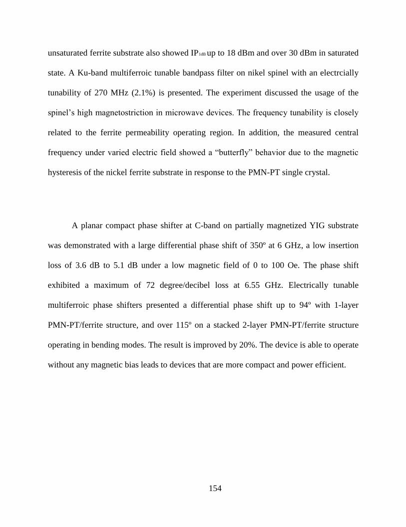
154
unsaturated ferrite substrate also showed IP1dB up to 18 dBm and over 30 dBm in saturated
state. A Ku-band multiferroic tunable bandpass filter on nikel spinel with an electrcially
tunability of 270 MHz (2.1%) is presented. The experiment discussed the usage of the
spinel‟s high magnetostriction in microwave devices. The frequency tunability is closely
related to the ferrite permeability operating region. In addition, the measured central
frequency under varied electric field showed a “butterfly” behavior due to the magnetic
hysteresis of the nickel ferrite substrate in response to the PMN-PT single crystal.
A planar compact phase shifter at C-band on partially magnetized YIG substrate
was demonstrated with a large differential phase shift of 350º at 6 GHz, a low insertion
loss of 3.6 dB to 5.1 dB under a low magnetic field of 0 to 100 Oe. The phase shift
exhibited a maximum of 72 degree/decibel loss at 6.55 GHz. Electrically tunable
multiferroic phase shifters presented a differential phase shift up to 94º with 1-layer
PMN-PT/ferrite structure, and over 115º on a stacked 2-layer PMN-PT/ferrite structure
operating in bending modes. The result is improved by 20%. The device is able to operate
without any magnetic bias leads to devices that are more compact and power efficient.
Related Documents