National Aeronautics and Space Administration Commercial Sensor Survey Fiscal Year 2008 Compendium Radiation Test Report Heidi N. Becker Michael D. Dolphin Dennis O. Thorbourn James W. Alexander Phil M. Salomon Jet Propulsion Laboratory Pasadena, California Jet Propulsion Laboratory California Institute of Technology Pasadena, California JPL Publication 08-26 10/08

Welcome message from author
This document is posted to help you gain knowledge. Please leave a comment to let me know what you think about it! Share it to your friends and learn new things together.
Transcript

National Aeronautics and Space Administration
Commercial Sensor Survey Fiscal Year 2008 Compendium
Radiation Test Report
Heidi N. Becker Michael D. Dolphin
Dennis O. Thorbourn James W. Alexander
Phil M. Salomon
Jet Propulsion Laboratory Pasadena, California
Jet Propulsion Laboratory California Institute of Technology
Pasadena, California
JPL Publication 08-26 10/08

National Aeronautics and Space Administration
Commercial Sensor Survey Fiscal Year 2008 Compendium
Radiation Test Report
NASA Electronic Parts and Packaging (NEPP) Program Office of Safety and Mission Assurance
Heidi N. Becker Michael D. Dolphin
Dennis O. Thorbourn James W. Alexander
Phil M. Salomon
Jet Propulsion Laboratory Pasadena, California
NASA WBS: 939904.01.11.30 JPL Project Number: 102197
Task Number: 3.21.4
Jet Propulsion Laboratory 4800 Oak Grove Drive Pasadena, CA 91109
http://nepp.nasa.gov
This research was carried out at the Jet Propulsion Laboratory, California Institute of
Technology, and was sponsored by the National Aeronautics and Space Administration
Electronic Parts and Packaging (NEPP) Program.
Reference herein to any specific commercial product, process, or service by trade name,
trademark, manufacturer, or otherwise, does not constitute or imply its endorsement by
the United States Government or the Jet Propulsion Laboratory, California Institute of
Technology.
Copyright 2008. California Institute of Technology. Government sponsorship
acknowledged.
ii

Table of Contents 1.0 Introduction............................................................................................................. 1 2.0 Sensors Selected for Radiation Testing .................................................................. 1
2.1 Micron......................................................................................................... 1 2.1.1 Micron MT9P031 (5 Mpixel, 1/2.5 inch, 2.2 μm) – “Micron
5MPX” ............................................................................................ 1 2.1.2 Micron MT9T031 (3.1 Mpixel, 1/2 inch, 3.2 μm) – “Micron
3MPX“ ............................................................................................ 1 2.1.3 Micron Evaluation Kit .................................................................... 1
2.2 OmniVision................................................................................................. 2 2.2.1 OV3630 (3.2 Mpixel, 1/3.2 inch, 2.2 μm) ...................................... 2
3.0 Test Bench .............................................................................................................. 3 3.1 Sensor Characterization Test Bench ........................................................... 3 3.2 Co-60 Irradiation Configuration ................................................................. 4
4.0 Characterization Approach ..................................................................................... 5 4.1 Manual and Auto......................................................................................... 5 4.2 Data Sets ..................................................................................................... 5 4.3 Analyzed Sensor Parameters....................................................................... 6
5.0 Radiation Test Levels ............................................................................................. 6 6.0 Radiation Test Conditions....................................................................................... 8 7.0 Micron Test Results ................................................................................................ 9
7.1 Parametric Characterizations (Manual) ...................................................... 9 7.1.1 Gain................................................................................................. 9 7.1.2 Dark Signal ................................................................................... 10 7.1.3 Dark Signal Non-Uniformity (DSNU).......................................... 16 7.1.4 Photo-Response Non-Uniformity ................................................. 18 7.1.5 Pixel Noise .................................................................................... 20
7.2 Bar Target Images (Auto) ......................................................................... 23 8.0 OmniVision Test Results ...................................................................................... 27
8.1 OV3630 Parametric Characterizations (Manual)...................................... 27 8.1.1 Dark Signal ................................................................................... 27 8.1.2 Dark Signal Non-Uniformity (DSNU).......................................... 28 8.1.3 Photo-Response Non-Uniformity (PRNU) ................................... 30 8.1.4 Pixel Noise .................................................................................... 30 8.1.5 Flickering Hot Pixels .................................................................... 31
8.2 Bar Target Images (Auto) ......................................................................... 33 9.0 Conclusions and Next Steps.................................................................................. 35 10.0 References............................................................................................................. 35 11.0 Appendix 1 – Sensor Selection Criteria [1] .......................................................... 36
iii

iv
Acronym List ADC Analog-to-Ditigal Converter CCD Charge Coupled Device CMOS Complementary Metal Oxide Semiconductor DDD Displacement Damage Dose DN Digital Number (analog-to-digital converter count) DSNU [Pixel] Dark Signal Non-Uniformity LED Light Emitting Diode OV OmniVision MOSFET Metal Oxide Semiconductor Field Effect Transistor NEPP NASA Electronic Parts and Packaging (Program) PRNU [Pixel] Photo Response Non-Uniformity RTS Random Telegraph Signal TID Total Ionizing Dose USAF United States Air Force
1.0 Introduction The NASA Electronic Parts and Packaging (NEPP) Program Sensor Technology Commercial Sensor Survey task is geared toward benefiting future NASA space missions with low-cost, short-duty-cycle, visible-wavelength imaging needs. Such applications could include imaging for educational outreach purposes or short surveys of spacecraft, planetary, or lunar surfaces. Under the task, inexpensive commercial grade CMOS sensors were surveyed in fiscal year 2007 (FY07) and three sensors were selected for total ionizing dose (TID) and displacement damage dose (DDD) tolerance testing. The selected sensors had to meet selection criteria chosen to support small, low-mass cameras that produce good resolution color images. These criteria were discussed in detail in [1], and are provided again in Appendix 1 of this document. This compendium provides results for all radiation testing performed in FY08 on the Micron and OmniVision sensors that were selected in FY07 for radiation tolerance testing.
2.0 Sensors Selected for Radiation Testing Following are brief descriptions of the selected sensors and the manufacturer-supplied evaluation kits used for our characterizations. Details of evaluation kit support software are proprietary to Micron and OmniVision and are not discussed in this document.
2.1 Micron 2.1.1 Micron MT9P031 (5 Mpixel, 1/2.5 inch, 2.2 μm) – “Micron 5MPX”
The MT9P031 is a 5-Mpixel, 1/2.5-inch optical format, CMOS sensor with a 2592(H) × 1944(V) color pixel array that employs a red-green-blue (RGB) Bayer pattern color filter. The pixel size is 2.2 μm × 2.2 μm. This product is marketed for applications that include high-resolution network cameras, wide field-of-view cameras, and hybrid video cameras with high resolution stills. Among its features are a 12-bit, on-chip analog-to-digital converter (ADC); 381-mW power consumption when imaging at full resolution and 14 frames-per-second; and low dark current and read noise [2].
2.1.2 Micron MT9T031 (3.1 Mpixel, 1/2 inch, 3.2 μm) – “Micron 3MPX“
The MT9T031 is a 3.1-Mpixel, 1/2-inch CMOS sensor with a 2048(H) × 1536(V) pixel array and RGB Bayer pattern color filter. The pixel size is 3.2 μm × 3.2 μm. This sensor has a 10-bit, on-chip ADC; 228-mW power consumption when imaging at full resolution and 12 frames per second; and low dark current and read noise. This sensor is also marketed for wide field-of-view cameras, video cameras, and high resolution stills [3].
2.1.3 Micron Evaluation Kit Evaluation of both Micron sensors was supported by Micron’s Demo2 Evaluation Hardware Kit (Figure 1) and accompanying DevWare software. This kit uses interchangeable camera headboards that are customized for each sensor product. The headboards for the Micron 5MPX and 3MPX were modified to include a test sample socket integrated with the camera’s optical barrel. This modification allowed many sensor samples to be evaluated using the same headboard electronics. The custom sockets were designed with a thermocouple access point to allow temperature monitoring of samples during characterization.
1
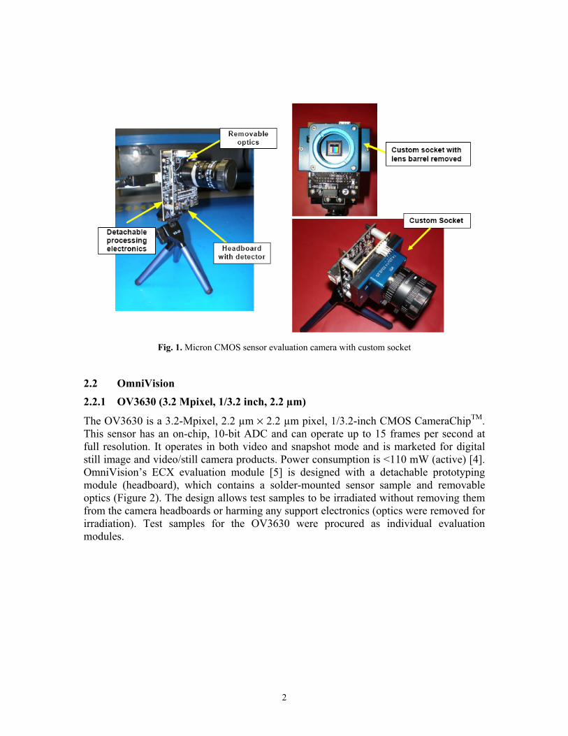
Fig. 1. Micron CMOS sensor evaluation camera with custom socket
2.2 OmniVision 2.2.1 OV3630 (3.2 Mpixel, 1/3.2 inch, 2.2 μm)
The OV3630 is a 3.2-Mpixel, 2.2 μm × 2.2 μm pixel, 1/3.2-inch CMOS CameraChipTM. This sensor has an on-chip, 10-bit ADC and can operate up to 15 frames per second at full resolution. It operates in both video and snapshot mode and is marketed for digital still image and video/still camera products. Power consumption is <110 mW (active) [4]. OmniVision’s ECX evaluation module [5] is designed with a detachable prototyping module (headboard), which contains a solder-mounted sensor sample and removable optics (Figure 2). The design allows test samples to be irradiated without removing them from the camera headboards or harming any support electronics (optics were removed for irradiation). Test samples for the OV3630 were procured as individual evaluation modules.
2
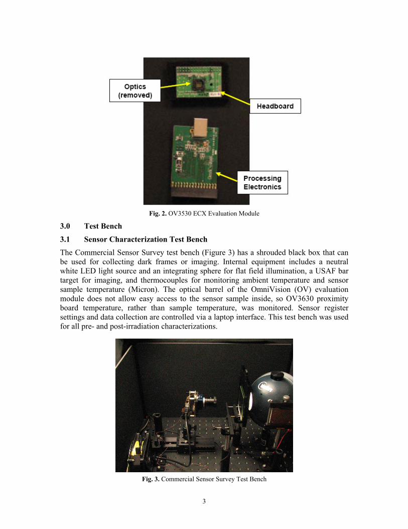
Fig. 2. OV3530 ECX Evaluation Module
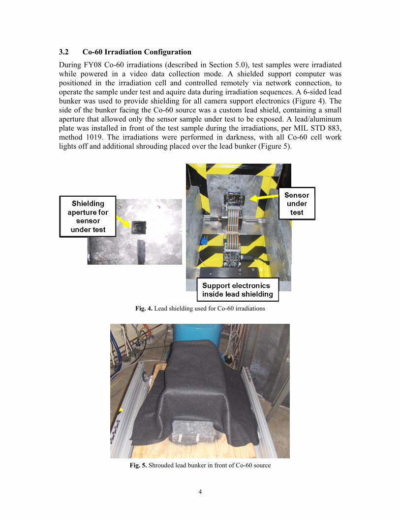
3.0 Test Bench 3.1 Sensor Characterization Test Bench The Commercial Sensor Survey test bench (Figure 3) has a shrouded black box that can be used for collecting dark frames or imaging. Internal equipment includes a neutral white LED light source and an integrating sphere for flat field illumination, a USAF bar target for imaging, and thermocouples for monitoring ambient temperature and sensor sample temperature (Micron). The optical barrel of the OmniVision (OV) evaluation module does not allow easy access to the sensor sample inside, so OV3630 proximity board temperature, rather than sample temperature, was monitored. Sensor register settings and data collection are controlled via a laptop interface. This test bench was used for all pre- and post-irradiation characterizations.
Fig. 3. Commercial Sensor Survey Test Bench
3
3.2 Co-60 Irradiation Configuration During FY08 Co-60 irradiations (described in Section 5.0), test samples were irradiated while powered in a video data collection mode. A shielded support computer was positioned in the irradiation cell and controlled remotely via network connection, to operate the sample under test and aquire data during irradiation sequences. A 6-sided lead bunker was used to provide shielding for all camera support electronics (Figure 4). The side of the bunker facing the Co-60 source was a custom lead shield, containing a small aperture that allowed only the sensor sample under test to be exposed. A lead/aluminum plate was installed in front of the test sample during the irradiations, per MIL STD 883, method 1019. The irradiations were performed in darkness, with all Co-60 cell work lights off and additional shrouding placed over the lead bunker (Figure 5).
Fig. 4. Lead shielding used for Co-60 irradiations
Fig. 5. Shrouded lead bunker in front of Co-60 source
4

4.0 Characterization Approach 4.1 Manual and Auto All three sensors are designed with on-chip image correction features to provide low noise performance (e.g., black-level calibration, analog and digital offset corrections, etc.). However, the function of these features is to subtract or adjust for device parameters that can change following radiation exposure. A good example is the correction of pixel dark signal, the rates of which increase with total ionizing dose (TID) and displacement damage dose (DDD). In order to identify the uncorrected radiation degradation in basic device parameters, and also to see how these effects could be corrected via on-chip image correction features, our approach to characterizing the radiation response of the three sensor technologies had two components:
1) Manual: Data collection with sensor register settings adjusted to control parameters that can influence characterization results:
a) Use of fixed exposure times, manual offset selection, and fixed internal signal chain gains (analog and digital), to ensure integrity of all pixel data without pixel or ADC saturation.
b) Disabled on-chip image correction features (such as black-level calibration/correction, noise reduction, and white balance) for accurate determination of dark signal rates, pixel noise, and photoresponse.
2) Auto: Data collection with sensor auto functions enabled to see how radiation degradation effects are corrected internally by the sensor.
Note that in a camera application, the camera designer would likely choose some combination of manually controlled and auto-controlled register settings, depending on the particular imaging need. For our data collection, default evaluation kit auto settings were used.
4.2 Data Sets The following data sets were collected pre- and post-irradiation:
1) Manual:
a) Dark frames collected at several different integration times (used for pixel dark signal rate, noise, and dark signal non-uniformity [DSNU] calculations).
b) Flat field images at several different integration times (used for photon transfer curves, noise, and photo response non-uniformity [PRNU] calculations).
c) Bar target images taken at best focus for different integration times (used for qualitative imaging assessment). One set of images was collected at the exposure time and gain settings that were chosen by the sensor during auto bar target image collection.
2) Auto:
a) Dark frames (at one auto exposure time chosen by the sensor; black-level calibration/correction and white balance enabled; gains automatically chosen by the sensor).
b) Flat field images (at one auto exposure time chosen by the sensor).
5

c) Bar target images taken at best focus (used for qualitative imaging assessment).
Each data set included five frames taken under identical conditions in rapid succession (the number of dark frames collected for the OV3630 was increased to 10 per data set during June 2008 proton testing and September 2008 Co-60 testing, in order to minimize the effect of noise on measurement error). Optically black reference pixel values were saved for every manual and auto data frame. All data were collected at ambient temperature.
4.3 Analyzed Sensor Parameters Mean Dark Signal Rate: The average pixel signal rate under un-illuminated conditions.
Local Pixel DSNU: The average rms value of pixel dark signal calculated over local 16 x 16 pixel windows. In our calculations, local DSNU was calculated on a color-wise basis (e.g., local DSNU calculated for only green1 pixels, red pixels, blue pixels, or green2 pixels) to remove the effects of any offsets between the four colors.
Pixel PRNU: The rms value of pixel photo response under flat field (uniform) illumination conditions.
Pixel Noise: The average rms signal value. The calculations in this report were performed using data taken under un-illuminated conditions with various integration times. Pixel noise under these conditions includes a combination of thermal dark current shot noise, output amplifier noise, on-chip electronic noise, and any uncorrected offset noise or pixel reset noise.
Gain: CMOS sensor (camera) gain in signal electrons/ADC unit (e/DN).
5.0 Radiation Test Levels Our radiation test levels were based on a range of displacement damage dose (DDD) and total ionizing dose (TID) levels that are considered typical for outreach or survey cameras in Earth orbit or Deep Space solar flare environments (e.g., Mars). These types of cameras typically have to compete with other payloads and flight system instruments, which may have higher priority for available shielding mass and strategic positioning on the spacecraft. The negotiated amount of shielding would depend on the priority of the camera’s data return, how early in the mission the camera would be expected to achieve its requirements, the relative radiation sensitivity of the sensor technology, and the risk to meeting performance requirements due to radiation degradation or transient noise.
In the environments considered, high energy protons are the dominant contributors to cumulative mission DDD and TID. 50-MeV protons were selected for our irradiations because this energy is representative of the typical radiation spectrum at the detector level, after having passed through instrument shielding. This allowed us to perform representative TID and DDD testing simultaneously. The radiation test levels listed in Table 1 show target TID levels and the corresponding 50-MeV proton test fluence and DDD in silicon.
6
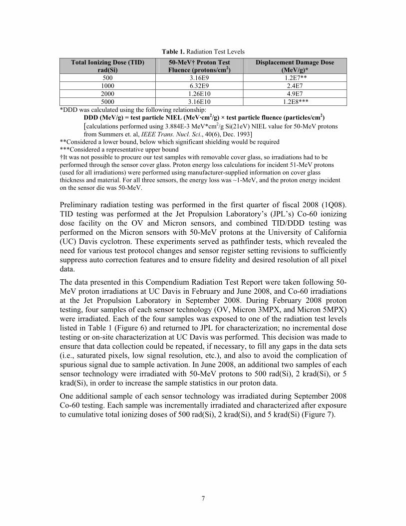
Table 1. Radiation Test Levels Total Ionizing Dose (TID)
rad(Si) 50-MeV† Proton Test Fluence (protons/cm2)
Displacement Damage Dose (MeV/g)*
500 3.16E9 1.2E7** 1000 6.32E9 2.4E7 2000 1.26E10 4.9E7 5000 3.16E10 1.2E8***
*DDD was calculated using the following relationship: DDD (MeV/g) = test particle NIEL (MeV·cm2/g) × test particle fluence (particles/cm2) [calculations performed using 3.884E-3 MeV*cm2/g Si(21eV) NIEL value for 50-MeV protons from Summers et. al, IEEE Trans. Nucl. Sci., 40(6), Dec. 1993]
**Considered a lower bound, below which significant shielding would be required ***Considered a representative upper bound †It was not possible to procure our test samples with removable cover glass, so irradiations had to be performed through the sensor cover glass. Proton energy loss calculations for incident 51-MeV protons (used for all irradiations) were performed using manufacturer-supplied information on cover glass thickness and material. For all three sensors, the energy loss was ~1-MeV, and the proton energy incident on the sensor die was 50-MeV.
Preliminary radiation testing was performed in the first quarter of fiscal 2008 (1Q08). TID testing was performed at the Jet Propulsion Laboratory’s (JPL’s) Co-60 ionizing dose facility on the OV and Micron sensors, and combined TID/DDD testing was performed on the Micron sensors with 50-MeV protons at the University of California (UC) Davis cyclotron. These experiments served as pathfinder tests, which revealed the need for various test protocol changes and sensor register setting revisions to sufficiently suppress auto correction features and to ensure fidelity and desired resolution of all pixel data.
The data presented in this Compendium Radiation Test Report were taken following 50-MeV proton irradiations at UC Davis in February and June 2008, and Co-60 irradiations at the Jet Propulsion Laboratory in September 2008. During February 2008 proton testing, four samples of each sensor technology (OV, Micron 3MPX, and Micron 5MPX) were irradiated. Each of the four samples was exposed to one of the radiation test levels listed in Table 1 (Figure 6) and returned to JPL for characterization; no incremental dose testing or on-site characterization at UC Davis was performed. This decision was made to ensure that data collection could be repeated, if necessary, to fill any gaps in the data sets (i.e., saturated pixels, low signal resolution, etc.), and also to avoid the complication of spurious signal due to sample activation. In June 2008, an additional two samples of each sensor technology were irradiated with 50-MeV protons to 500 rad(Si), 2 krad(Si), or 5 krad(Si), in order to increase the sample statistics in our proton data.
One additional sample of each sensor technology was irradiated during September 2008 Co-60 testing. Each sample was incrementally irradiated and characterized after exposure to cumulative total ionizing doses of 500 rad(Si), 2 krad(Si), and 5 krad(Si) (Figure 7).
7
Proton Test Samples (30)
Micron 5MPX Samples (10)
Micron 3MPX Samples (10)
OV3630 Samples (10)
500 rad(Si)/1.2E7 MeV/g (50-MeV protons) (3)
1 krad(Si)/2.4E7 MeV/g (50-MeV protons) (1)
2 krad(Si)/4.9E7 MeV/g (50-MeV protons) (3)
5 krad(Si)/1.2E8 MeV/g (50-MeV protons) (3)
500 rad(Si)/1.2E7 MeV/g (50-MeV protons) (3)
1 krad(Si)/2.4E7 MeV/g (50-MeV protons) (1)
2 krad(Si)/4.9E7 MeV/g (50-MeV protons) (3)
5 krad(Si)/1.2E8 MeV/g (50-MeV protons) (3)
500 rad(Si)/1.2E7 MeV/g (50-MeV protons) (3)
1 krad(Si)/2.4E7 MeV/g (50-MeV protons) (1)
2 krad(Si)/4.9E7 MeV/g (50-MeV protons) (3)
5 krad(Si)/1.2E8 MeV/g (50-MeV protons) (3)
Fig. 6. 50-MeV Proton Radiation Test Sample Allocation
Co-60 Test Samples
(3)
Micron 5MPX Samples (1)
Micron 3MPX Samples (1)
OV3630 Samples (1)
500 rad(Si) (cumulative)
500 rad(Si) (cumulative)
500 rad(Si) (cumulative)
2 krad(Si) (cumulative)
2 krad(Si) (cumulative)
2 krad(Si) (cumulative)
5 krad(Si)
(cumulative) 5 krad(Si)
(cumulative) 5 krad(Si)
(cumulative)
Fig. 7. Co-60 Radiation Test Sample Allocation
6.0 Radiation Test Conditions Proton test samples were irradiated unpowered with all leads shorted to ground. Unpowered irradiation was chosen for proton testing because it is considered representative of the low-duty cycles of the camera applications addressed by this study. Characterizations were performed within several weeks following irradiation.
Co-60 irradiations were performed with samples powered in a video data collection mode. A 10 rad(Si)/s dose rate was used. Following irradiation to each target TID increment, samples were removed from the irradiation camera support circuitry and transferred to the characterization test bench for post-irradiation characterization.
8

Characterizations were completed within four hours following each incremental TID exposure.
Biased Co-60 irradiation is not as representative of potential flight conditions as unbiased irradiation with protons. It imparts only a negligible level of DDD, and the likelihood that an outreach or survey camera would be in an observation mode during an in-flight solar flare situation is small. However, CMOS technologies often experience a larger degree of degradation when irradiated in a powered condition, and charge coupled device (CCD) imagers have previously been seen to experience TID-related parameter shifts that are a factor of 2 to 3 higher when irradiations are performed on powered vs. un-powered samples [6]. It was decided to perform biased Co-60 irradiations because such promising performance was seen in our three sensor technologies following unbiased proton irradiation in February 2008 and biased Co-60 irradiation was relatively easy for us to execute within FY08. Co-60 data analysis was limited to mean dark rate calculations and qualitative assessment of imaging performance following irradiation.
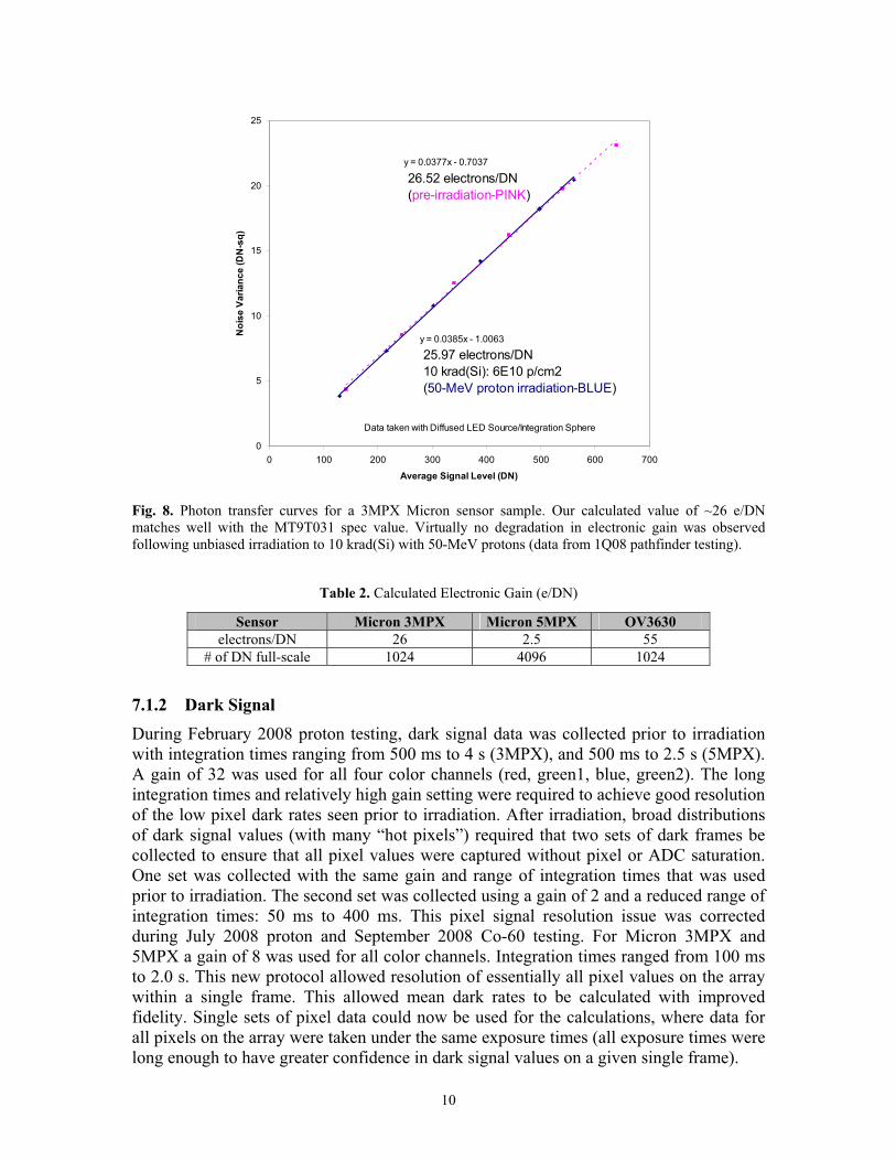
7.0 Micron Test Results 7.1 Parametric Characterizations (Manual) 7.1.1 Gain Data in this report are expressed in terms of digital number (DN; analog-to-digital converter count). The conversion from DN to electrons can be found by plotting the signal variance (DN2) vs. average signal level under flat field illumination conditions. For the range of signal levels dominated by shot noise, electron gain is given by the slope of this linear region:
e/DN = )()(
22 DNDNsignal
σ (1)
An example of this technique is shown in Figure 8 for the Micron 3MPX sensor. Similar calculations were performed to determine e/DN for the Micron 5MPX sensor and the OV3630. Results for all three sensors are shown in Table 2.
9
y = 0.0385x - 1.0063
y = 0.0377x - 0.7037
0
5
10
15
20
25
0 100 200 300 400 500 600 700
Average Signal Level (DN)
Noi
se V
aria
nce
(DN
-sq)
25.97 electrons/DN10 krad(Si): 6E10 p/cm2(50-MeV proton irradiation-BLUE)
Data taken with Diffused LED Source/Integration Sphere
26.52 electrons/DN(pre-irradiation-PINK)
Fig. 8. Photon transfer curves for a 3MPX Micron sensor sample. Our calculated value of ~26 e/DN matches well with the MT9T031 spec value. Virtually no degradation in electronic gain was observed following unbiased irradiation to 10 krad(Si) with 50-MeV protons (data from 1Q08 pathfinder testing).
Table 2. Calculated Electronic Gain (e/DN)
Sensor Micron 3MPX Micron 5MPX OV3630 electrons/DN 26 2.5 55
# of DN full-scale 1024 4096 1024 7.1.2 Dark Signal During February 2008 proton testing, dark signal data was collected prior to irradiation with integration times ranging from 500 ms to 4 s (3MPX), and 500 ms to 2.5 s (5MPX). A gain of 32 was used for all four color channels (red, green1, blue, green2). The long integration times and relatively high gain setting were required to achieve good resolution of the low pixel dark rates seen prior to irradiation. After irradiation, broad distributions of dark signal values (with many “hot pixels”) required that two sets of dark frames be collected to ensure that all pixel values were captured without pixel or ADC saturation. One set was collected with the same gain and range of integration times that was used prior to irradiation. The second set was collected using a gain of 2 and a reduced range of integration times: 50 ms to 400 ms. This pixel signal resolution issue was corrected during July 2008 proton and September 2008 Co-60 testing. For Micron 3MPX and 5MPX a gain of 8 was used for all color channels. Integration times ranged from 100 ms to 2.0 s. This new protocol allowed resolution of essentially all pixel values on the array within a single frame. This allowed mean dark rates to be calculated with improved fidelity. Single sets of pixel data could now be used for the calculations, where data for all pixels on the array were taken under the same exposure times (all exposure times were long enough to have greater confidence in dark signal values on a given single frame).
10
For all pre- and post-irradiation data sets, five frames were taken at each integration time. From each set of five frames, an average frame was calculated on a pixel-by-pixel basis. The mean dark rate was calculated for each pixel position by taking the difference of the average dark signal at two integration times, dividing by the difference in integration time, and normalizing for a gain of 1. In order to calculate the mean dark rate for the entire array from the February 2008 proton data, pixel information from the two post-irradiation data sets had to be merged. The majority of pixels had post-irradiation dark rates that were low enough to use the data collected with the longer integration times and higher gain setting, but dark rates for the hotter pixels were calculated using the data collected with lower gain and integration times. Using this approach, the mean dark rate over the entire image was calculated by averaging the mean dark rates of the individual pixels. For the June 2008 proton and September 2008 Co-60 data, the mean dark rate over the array was calculated by simply averaging the values of a single set of individual pixel mean dark rates.
Figures 9 and 10 show the increase in mean dark rate as a function of ionizing dose for the Micron 3MPX and 5MPX sensors, respectively. Rates are given in DN (ADC count) per pixel per second. See Section 7.1.1 for conversions from DN to electrons for the 3MPX and 5MPX. Lines are fits to the linear trends seen in our data at these radiation levels. The 3MPX 5 krad(Si) data point from the February 2008 proton test (Figure 9) is not included in the fit to the February 2008 data. We believe the calculation of the mean dark rate at this level, where a significant number of hot pixels was present, was skewed by the use of multiple data sets with differing gain settings (as described previously). The June 2008 proton data are considered more representative of the general behavior of the 3MPX because of the improved characterization approach used for that test.
11
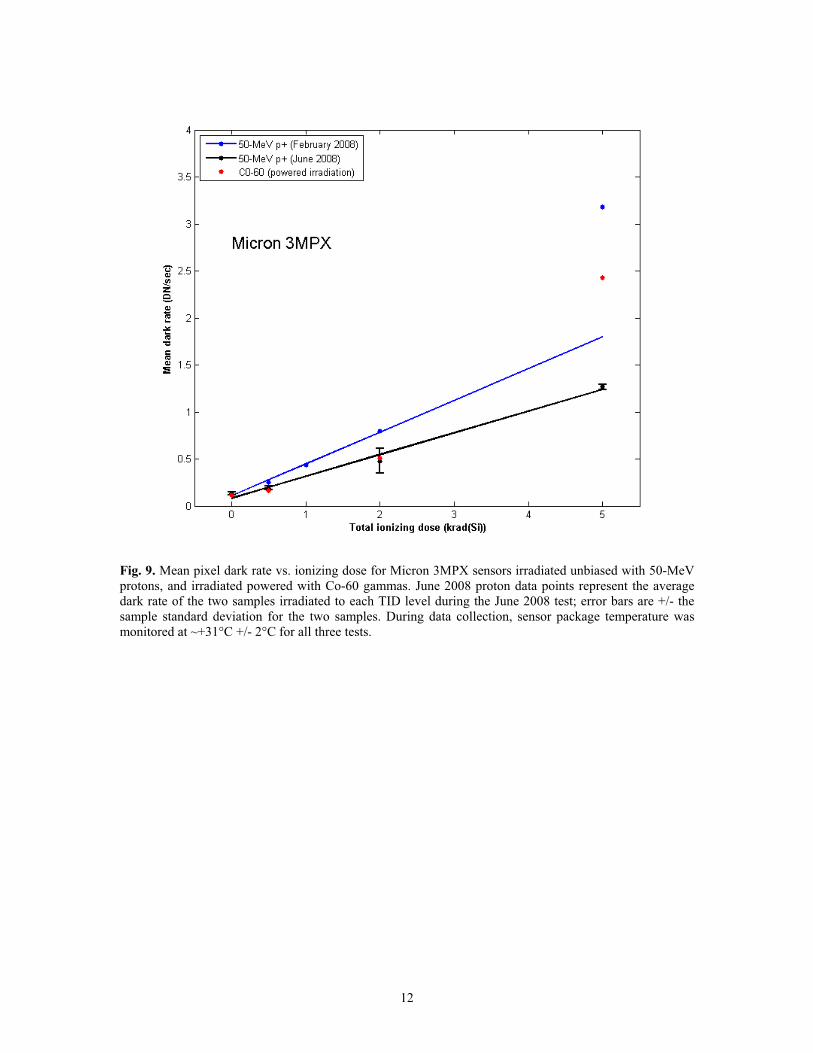
Fig. 9. Mean pixel dark rate vs. ionizing dose for Micron 3MPX sensors irradiated unbiased with 50-MeV protons, and irradiated powered with Co-60 gammas. June 2008 proton data points represent the average dark rate of the two samples irradiated to each TID level during the June 2008 test; error bars are +/- the sample standard deviation for the two samples. During data collection, sensor package temperature was monitored at ~+31°C +/- 2°C for all three tests.
12
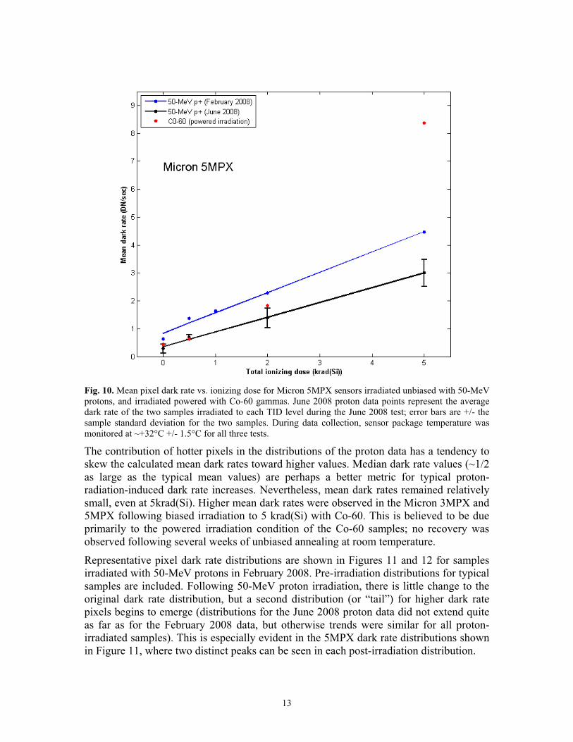
Fig. 10. Mean pixel dark rate vs. ionizing dose for Micron 5MPX sensors irradiated unbiased with 50-MeV protons, and irradiated powered with Co-60 gammas. June 2008 proton data points represent the average dark rate of the two samples irradiated to each TID level during the June 2008 test; error bars are +/- the sample standard deviation for the two samples. During data collection, sensor package temperature was monitored at ~+32°C +/- 1.5°C for all three tests.
The contribution of hotter pixels in the distributions of the proton data has a tendency to skew the calculated mean dark rates toward higher values. Median dark rate values (~1/2 as large as the typical mean values) are perhaps a better metric for typical proton-radiation-induced dark rate increases. Nevertheless, mean dark rates remained relatively small, even at 5krad(Si). Higher mean dark rates were observed in the Micron 3MPX and 5MPX following biased irradiation to 5 krad(Si) with Co-60. This is believed to be due primarily to the powered irradiation condition of the Co-60 samples; no recovery was observed following several weeks of unbiased annealing at room temperature.
Representative pixel dark rate distributions are shown in Figures 11 and 12 for samples irradiated with 50-MeV protons in February 2008. Pre-irradiation distributions for typical samples are included. Following 50-MeV proton irradiation, there is little change to the original dark rate distribution, but a second distribution (or “tail”) for higher dark rate pixels begins to emerge (distributions for the June 2008 proton data did not extend quite as far as for the February 2008 data, but otherwise trends were similar for all proton-irradiated samples). This is especially evident in the 5MPX dark rate distributions shown in Figure 11, where two distinct peaks can be seen in each post-irradiation distribution.
13
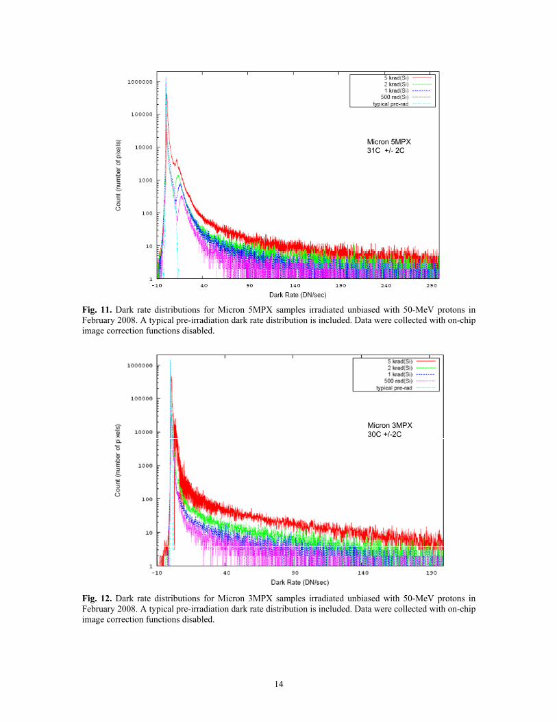
Micron 5MPX31C +/- 2CMicron 5MPX31C +/- 2C
Fig. 11. Dark rate distributions for Micron 5MPX samples irradiated unbiased with 50-MeV protons in February 2008. A typical pre-irradiation dark rate distribution is included. Data were collected with on-chip image correction functions disabled.
Micron 3MPX30C +/-2CMicron 3MPX30C +/-2C
Fig. 12. Dark rate distributions for Micron 3MPX samples irradiated unbiased with 50-MeV protons in February 2008. A typical pre-irradiation dark rate distribution is included. Data were collected with on-chip image correction functions disabled.
14

Figures 13 and 14 are semi-log plots of (1 - cumulative distribution function) for pixel dark rates seen after each irradiation level. Pre-irradiation data are also presented for a typical sample. This plotting format allows the percentage of pixels with dark rates greater than a given value to be compared for different irradiation levels. The increased percentage of hotter pixels at the higher irradiation levels is particularly evident in the 5MPX data. For both sensors, the increased numbers of higher dark rate pixels scales with proton fluence.
Fig. 13. Percentage of Micron 5MPX pixels with dark rates above a given rate. Data are from the February
2008 50-MeV proton test.
15

Fig. 14. Percentage of Micron 3MPX pixels with dark rates above a given rate. Data are from the February
2008 50-MeV proton test.
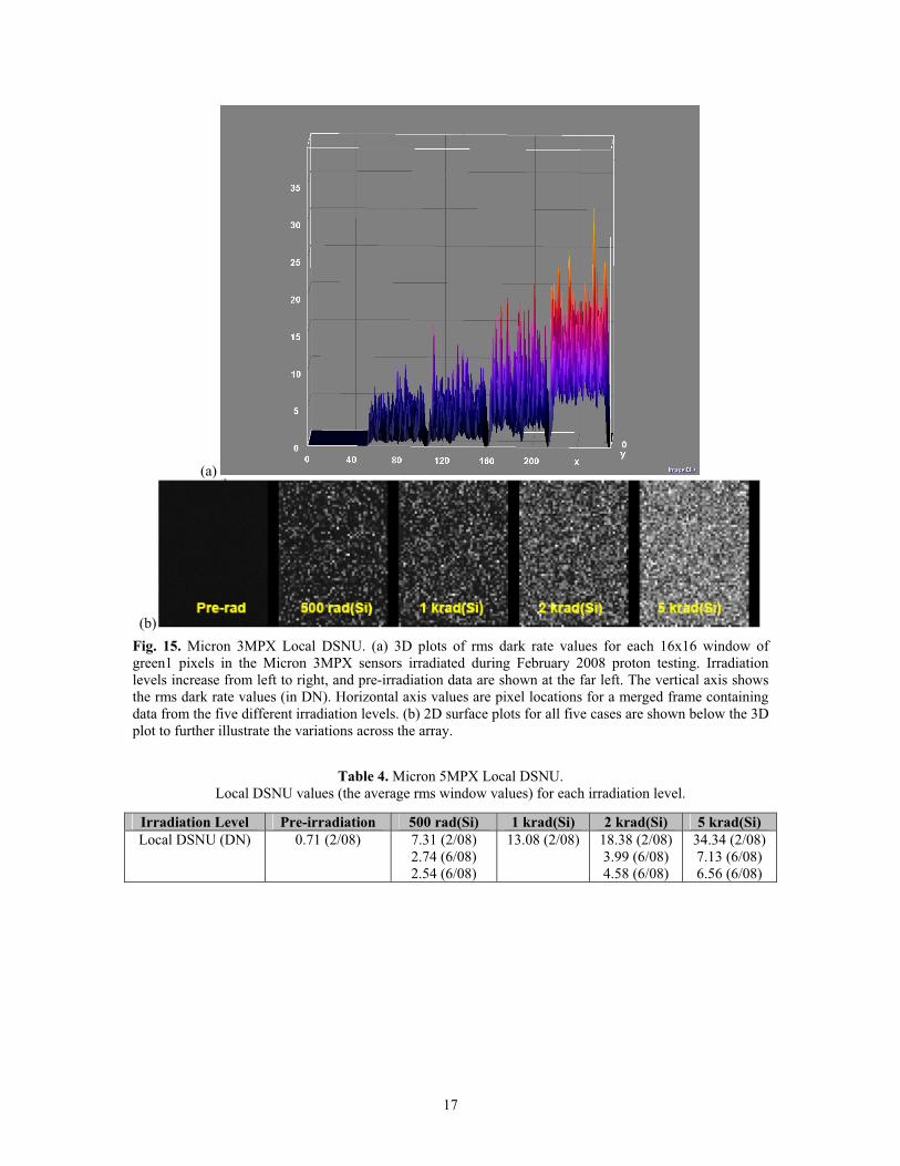
7.1.3 Dark Signal Non-Uniformity (DSNU) Local DSNU was calculated for green1 pixels by dividing the array into several 16x16 green1 “windows” and calculating the rms dark rate value over each window (only February and June 2008 proton data were used for this analysis). The average rms value for all windows (the “Local DSNU”) represents the typical DSNU that could impact local image quality. These analysis results are presented below in three different formats to illustrate the increase in DSNU from the pre-irradiation case to each irradiation level (Table 3, Figure 15, Table 4, and Figure 16):
1) A table of the calculated local DSNU 2) A 3D plot of the individual 16x16 window rms dark rate values 3) A 2D surface plot of the window rms values
Table 3. Micron 3MPX Local DSNU. Local DSNU values (the average rms window values) for each irradiation level.
Irradiation Level Pre-irradiation 500 rad(Si) 1 krad(Si) 2 krad(Si) 5 krad(Si) Local DSNU (DN)
0.181 (2/08) 1.88 (2/08)
0.55 (6/08) 0.59 (6/08)
2.80 (2/08)
5.15 (2/08) 1.15 (6/08) 1.16 (6/08)
10.97 (2/08) 1.69 (6/08) 1.76 (6/08)
16
(a)
(b)
Fig. 15. Micron 3MPX Local DSNU. (a) 3D plots of rms dark rate values for each 16x16 window of green1 pixels in the Micron 3MPX sensors irradiated during February 2008 proton testing. Irradiation levels increase from left to right, and pre-irradiation data are shown at the far left. The vertical axis shows the rms dark rate values (in DN). Horizontal axis values are pixel locations for a merged frame containing data from the five different irradiation levels. (b) 2D surface plots for all five cases are shown below the 3D plot to further illustrate the variations across the array.
Table 4. Micron 5MPX Local DSNU.
Local DSNU values (the average rms window values) for each irradiation level.
Irradiation Level Pre-irradiation 500 rad(Si) 1 krad(Si) 2 krad(Si) 5 krad(Si) Local DSNU (DN) 0.71 (2/08) 7.31 (2/08)
2.74 (6/08) 2.54 (6/08)
13.08 (2/08) 18.38 (2/08) 3.99 (6/08) 4.58 (6/08)
34.34 (2/08) 7.13 (6/08) 6.56 (6/08)
17
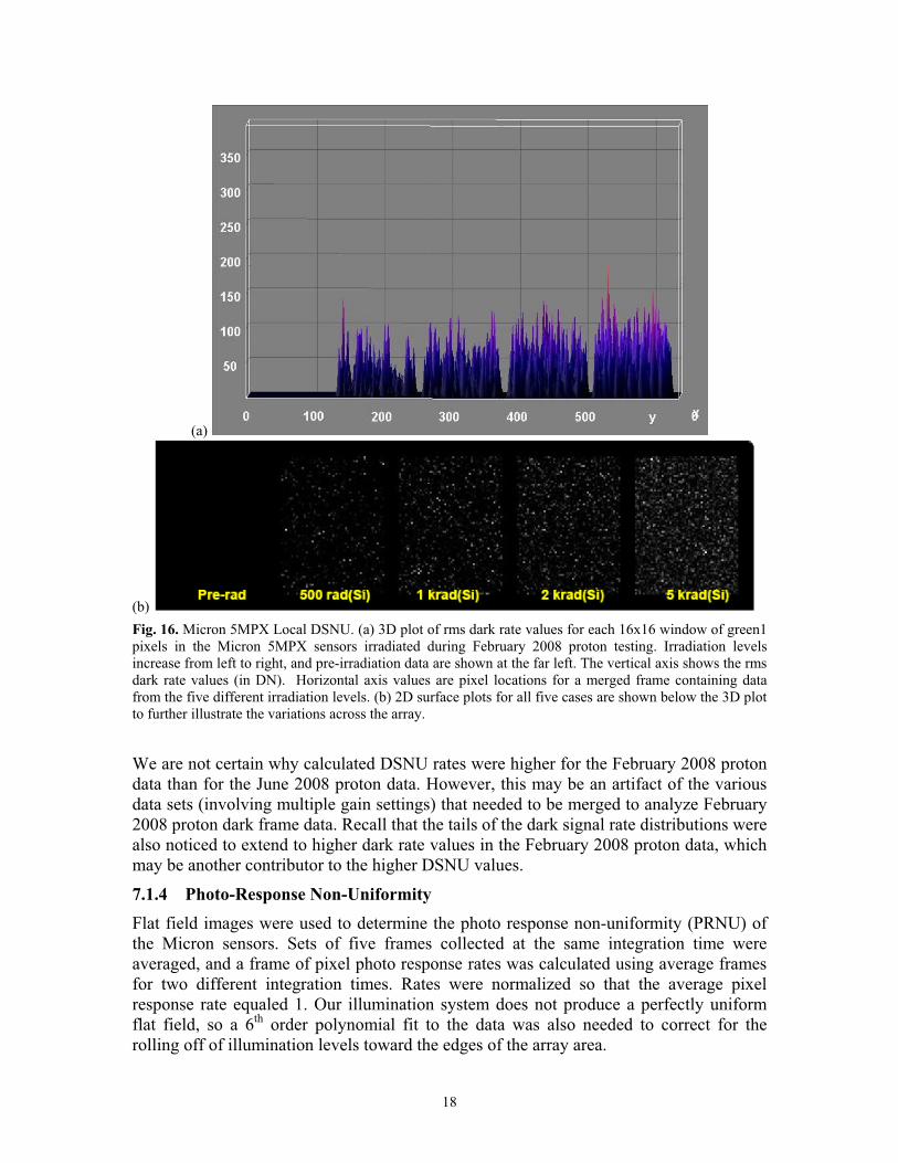
(a)
(b) Fig. 16. Micron 5MPX Local DSNU. (a) 3D plot of rms dark rate values for each 16x16 window of green1 pixels in the Micron 5MPX sensors irradiated during February 2008 proton testing. Irradiation levels increase from left to right, and pre-irradiation data are shown at the far left. The vertical axis shows the rms dark rate values (in DN). Horizontal axis values are pixel locations for a merged frame containing data from the five different irradiation levels. (b) 2D surface plots for all five cases are shown below the 3D plot to further illustrate the variations across the array.
We are not certain why calculated DSNU rates were higher for the February 2008 proton data than for the June 2008 proton data. However, this may be an artifact of the various data sets (involving multiple gain settings) that needed to be merged to analyze February 2008 proton dark frame data. Recall that the tails of the dark signal rate distributions were also noticed to extend to higher dark rate values in the February 2008 proton data, which may be another contributor to the higher DSNU values.
7.1.4 Photo-Response Non-Uniformity Flat field images were used to determine the photo response non-uniformity (PRNU) of the Micron sensors. Sets of five frames collected at the same integration time were averaged, and a frame of pixel photo response rates was calculated using average frames for two different integration times. Rates were normalized so that the average pixel response rate equaled 1. Our illumination system does not produce a perfectly uniform flat field, so a 6th order polynomial fit to the data was also needed to correct for the rolling off of illumination levels toward the edges of the array area.
18
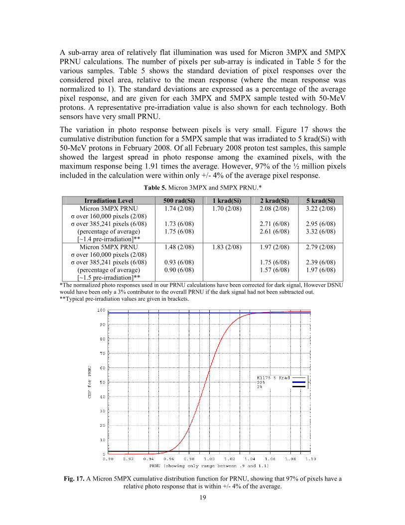
A sub-array area of relatively flat illumination was used for Micron 3MPX and 5MPX PRNU calculations. The number of pixels per sub-array is indicated in Table 5 for the various samples. Table 5 shows the standard deviation of pixel responses over the considered pixel area, relative to the mean response (where the mean response was normalized to 1). The standard deviations are expressed as a percentage of the average pixel response, and are given for each 3MPX and 5MPX sample tested with 50-MeV protons. A representative pre-irradiation value is also shown for each technology. Both sensors have very small PRNU.
The variation in photo response between pixels is very small. Figure 17 shows the cumulative distribution function for a 5MPX sample that was irradiated to 5 krad(Si) with 50-MeV protons in February 2008. Of all February 2008 proton test samples, this sample showed the largest spread in photo response among the examined pixels, with the maximum response being 1.91 times the average. However, 97% of the ½ million pixels included in the calculation were within only +/- 4% of the average pixel response.
Table 5. Micron 3MPX and 5MPX PRNU.*
*The normalized photo responses used in our PRNU calculations have been corrected for dark signal, However DSNU would have been only a 3% contributor to the overall PRNU if the dark signal had not been subtracted out.
Irradiation Level 500 rad(Si) 1 krad(Si) 2 krad(Si) 5 krad(Si) Micron 3MPX PRNU
� over 160,000 pixels (2/08) � over 385,241 pixels (6/08)
(percentage of average) [~1.4 pre-irradiation]**
1.74 (2/08)
1.73 (6/08) 1.75 (6/08)
1.70 (2/08)
2.08 (2/08)
2.71 (6/08) 2.61 (6/08)
3.22 (2/08)
2.95 (6/08) 3.32 (6/08)
Micron 5MPX PRNU
� over 160,000 pixels (2/08) � over 385,241 pixels (6/08)
(percentage of average) [~1.5 pre-irradiation]**
1.48 (2/08)
0.93 (6/08) 0.90 (6/08)
1.83 (2/08)
1.97 (2/08)
1.75 (6/08) 1.57 (6/08)
2.79 (2/08)
2.39 (6/08) 1.97 (6/08)
**Typical pre-irradiation values are given in brackets.
Fig. 17. A Micron 5MPX cumulative distribution function for PRNU, showing that 97% of pixels have a
relative photo response that is within +/- 4% of the average.
19

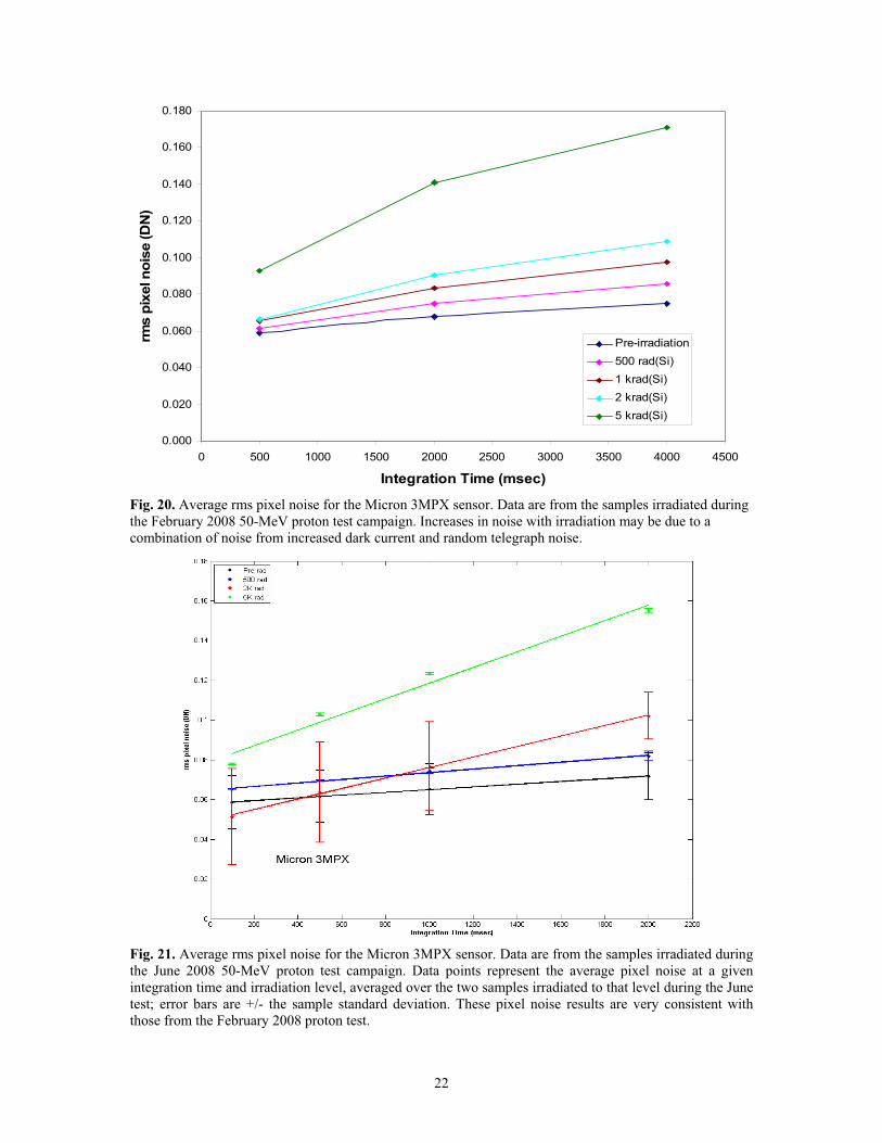
7.1.5 Pixel Noise The average rms pixel noise was calculated from dark frame data (five frames were taken at each integration time). As mentioned previously, pixel noise under these conditions includes a combination of thermal dark current shot noise, output amplifier noise, on-chip electronic noise, and any uncorrected offset noise or pixel reset noise (also see Section 8.1.5 on the importance of random telegraph noise). Pixel noise is shown in Figure 18 (February 2008 proton test) and Figure 19 (June 2008 proton test) for the Micron 5MPX. Similar plots for the Micron 3MPX are shown in Figures 20 and 21. June 2008 test data points represent the average pixel noise at a given integration time and irradiation level, averaged over the two samples irradiated to that level during the June test; error bars are +/- the sample standard deviation. February and June 2008 data are plotted on separate figures for clarity, but it is easily seen that the pixel noise results were very consistent between test samples from the two proton test campaigns. Pixel noise was seen to increase with integration time, which may be due to the presence of increased amounts of thermally generated dark signal for longer integration times. Increased noise is also seen when data taken at the same integration time are compared for increasing levels of ionizing dose. Increases in noise with irradiation may be due to a combination of increased dark current and random telegraph noise.
0.000
0.100
0.200
0.300
0.400
0.500
0.600
0.700
0 500 1000 1500 2000 2500 3000
Integration Time (msec)
rms
pixe
l noi
se (D
N)
Pre-irradiation500 rad(Si)1 krad(Si)2 krad(Si)5 krad(Si)
Fig. 18. Average rms pixel noise for the Micron 5MPX sensor. Data are from the samples irradiated during the February 2008 50-MeV proton test campaign. Increases in noise with irradiation may be due to a combination of noise from increased dark current and random telegraph noise.
20

Fig. 19. Average rms pixel noise for the Micron 5MPX sensor. Data are from the samples irradiated during the June 2008 50-MeV proton test campaign. Data points represent the average pixel noise at a given integration time and irradiation level, averaged over the two samples irradiated to that level during the June test; error bars are +/- the sample standard deviation. These pixel noise results are very consistent with those from the February 2008 proton test.
21
0.000
0.020
0.040
0.060
0.080
0.100
0.120
0.140
0.160
0.180
0 500 1000 1500 2000 2500 3000 3500 4000 4500
Integration Time (msec)
rms
pixe
l noi
se (D
N)
Pre-irradiation500 rad(Si)1 krad(Si)2 krad(Si)5 krad(Si)
Fig. 20. Average rms pixel noise for the Micron 3MPX sensor. Data are from the samples irradiated during the February 2008 50-MeV proton test campaign. Increases in noise with irradiation may be due to a combination of noise from increased dark current and random telegraph noise.
Fig. 21. Average rms pixel noise for the Micron 3MPX sensor. Data are from the samples irradiated during the June 2008 50-MeV proton test campaign. Data points represent the average pixel noise at a given integration time and irradiation level, averaged over the two samples irradiated to that level during the June test; error bars are +/- the sample standard deviation. These pixel noise results are very consistent with those from the February 2008 proton test.
22
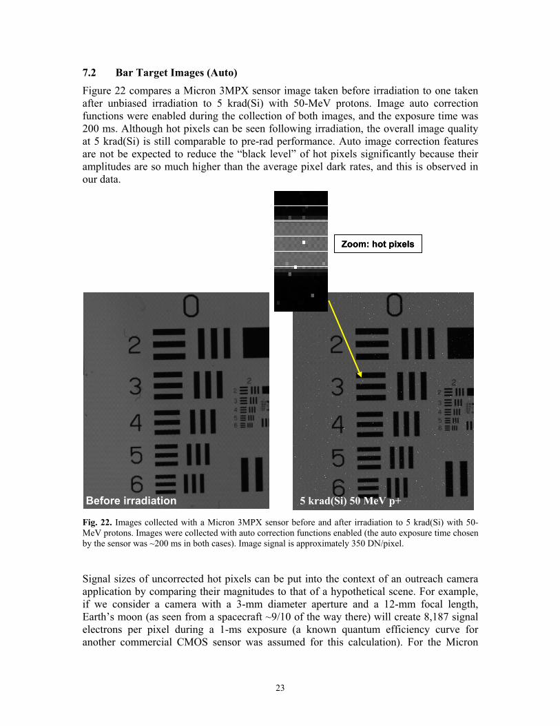
7.2 Bar Target Images (Auto) Figure 22 compares a Micron 3MPX sensor image taken before irradiation to one taken after unbiased irradiation to 5 krad(Si) with 50-MeV protons. Image auto correction functions were enabled during the collection of both images, and the exposure time was 200 ms. Although hot pixels can be seen following irradiation, the overall image quality at 5 krad(Si) is still comparable to pre-rad performance. Auto image correction features are not be expected to reduce the “black level” of hot pixels significantly because their amplitudes are so much higher than the average pixel dark rates, and this is observed in our data.
Before irradiation 5 krad(Si) 50 MeV p+
Zoom: hot pixels
Before irradiation 5 krad(Si) 50 MeV p+
Zoom: hot pixels
Fig. 22. Images collected with a Micron 3MPX sensor before and after irradiation to 5 krad(Si) with 50-MeV protons. Images were collected with auto correction functions enabled (the auto exposure time chosen by the sensor was ~200 ms in both cases). Image signal is approximately 350 DN/pixel.
Signal sizes of uncorrected hot pixels can be put into the context of an outreach camera application by comparing their magnitudes to that of a hypothetical scene. For example, if we consider a camera with a 3-mm diameter aperture and a 12-mm focal length, Earth’s moon (as seen from a spacecraft ~9/10 of the way there) will create 8,187 signal electrons per pixel during a 1-ms exposure (a known quantum efficiency curve for another commercial CMOS sensor was assumed for this calculation). For the Micron
23
3MPX sensor, this corresponds to a signal of 315 DN per pixel. As can be seen in the example in Figure 14, after irradiation to 5 krad(Si), approximately 0.03% of pixels have a dark rate that is at least 315 DN/second. With a 1-ms integration time, the dark signal contributed to the image would be only 0.3 DN per pixel, much less than the signal generated by the scene. Comparison of manual and auto images is complex because more than one image correction variable is involved. Black-level calibration and the resultant digital offset correction would be expected to correct for the average dark signal rate increases seen after irradiation. However, analysis of this correction needs to be considered along with the analog offset corrections that are also made on a color-wise basis before the digital black-level correction takes place.
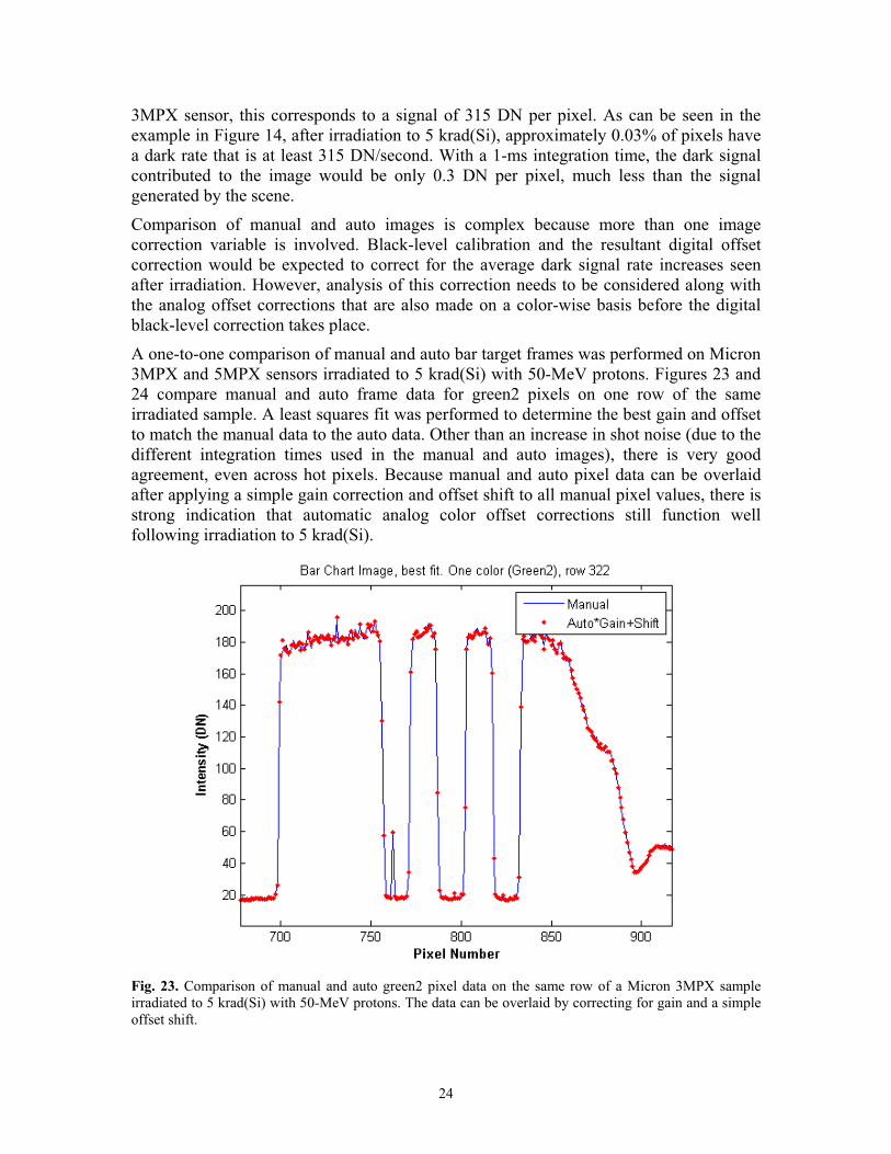
A one-to-one comparison of manual and auto bar target frames was performed on Micron 3MPX and 5MPX sensors irradiated to 5 krad(Si) with 50-MeV protons. Figures 23 and 24 compare manual and auto frame data for green2 pixels on one row of the same irradiated sample. A least squares fit was performed to determine the best gain and offset to match the manual data to the auto data. Other than an increase in shot noise (due to the different integration times used in the manual and auto images), there is very good agreement, even across hot pixels. Because manual and auto pixel data can be overlaid after applying a simple gain correction and offset shift to all manual pixel values, there is strong indication that automatic analog color offset corrections still function well following irradiation to 5 krad(Si).
Fig. 23. Comparison of manual and auto green2 pixel data on the same row of a Micron 3MPX sample irradiated to 5 krad(Si) with 50-MeV protons. The data can be overlaid by correcting for gain and a simple offset shift.
24

Additional qualitative assessment of analog color offset functionality may be made by comparing auto images of a colored scene taken with unirradiated samples and samples irradiated to 5 krad(Si). Figure 25 compares color images taken with an unirradiated Micron 5MPX sensor and one that has been irradiated to 5 krad(Si) with 50-MeV protons under the same imaging conditions. The color and overall quality of the images is seen to be very similar.
Fig. 24. Comparison of manual and auto green2 pixel data on the same row of a Micron 5MPX sample irradiated to 5 krad(Si) with 50-MeV protons. The data can be overlaid by correcting for gain and a simple offset shift.
Fig. 25. Comparison of color images collected with an unirradiated Micron 5MPX sensor and one that has been irradiated to 5 krad(Si) with 50-MeV protons. The images were collected with auto correction functions enabled and are qualitatively very similar.
25
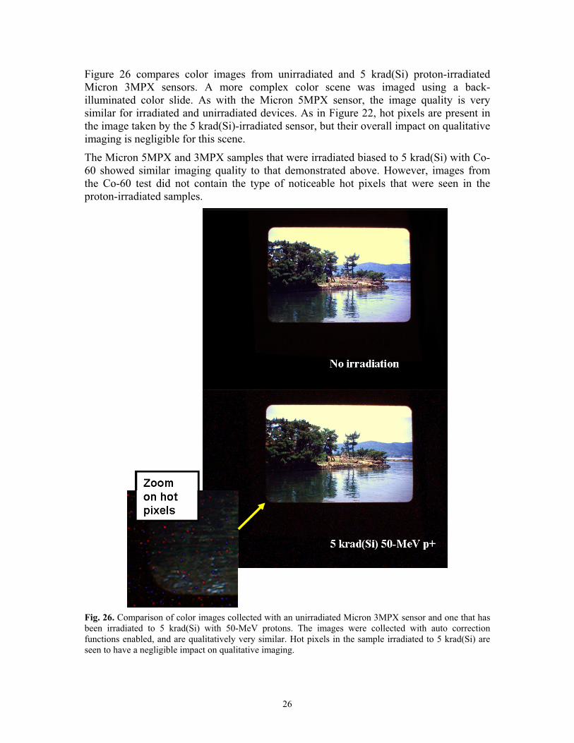
Figure 26 compares color images from unirradiated and 5 krad(Si) proton-irradiated Micron 3MPX sensors. A more complex color scene was imaged using a back-illuminated color slide. As with the Micron 5MPX sensor, the image quality is very similar for irradiated and unirradiated devices. As in Figure 22, hot pixels are present in the image taken by the 5 krad(Si)-irradiated sensor, but their overall impact on qualitative imaging is negligible for this scene.
The Micron 5MPX and 3MPX samples that were irradiated biased to 5 krad(Si) with Co-60 showed similar imaging quality to that demonstrated above. However, images from the Co-60 test did not contain the type of noticeable hot pixels that were seen in the proton-irradiated samples.
Fig. 26. Comparison of color images collected with an unirradiated Micron 3MPX sensor and one that has been irradiated to 5 krad(Si) with 50-MeV protons. The images were collected with auto correction functions enabled, and are qualitatively very similar. Hot pixels in the sample irradiated to 5 krad(Si) are seen to have a negligible impact on qualitative imaging.
26
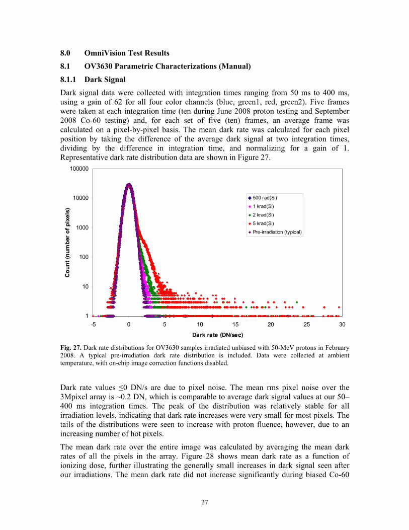
8.0 OmniVision Test Results 8.1 OV3630 Parametric Characterizations (Manual) 8.1.1 Dark Signal Dark signal data were collected with integration times ranging from 50 ms to 400 ms, using a gain of 62 for all four color channels (blue, green1, red, green2). Five frames were taken at each integration time (ten during June 2008 proton testing and September 2008 Co-60 testing) and, for each set of five (ten) frames, an average frame was calculated on a pixel-by-pixel basis. The mean dark rate was calculated for each pixel position by taking the difference of the average dark signal at two integration times, dividing by the difference in integration time, and normalizing for a gain of 1. Representative dark rate distribution data are shown in Figure 27.
1
10
100
1000
10000
100000
-5 0 5 10 15 20 25 30
Dark rate (DN/sec)
Coun
t (nu
mbe
r of
pix
els)
500 rad(Si)
1 krad(Si)
2 krad(Si)
5 krad(Si)
Pre-irradiation (typical)
Fig. 27. Dark rate distributions for OV3630 samples irradiated unbiased with 50-MeV protons in February
ark rate values �0 DN/s are due to pixel noise. The mean rms pixel noise over the
age was calculated by averaging the mean dark
2008. A typical pre-irradiation dark rate distribution is included. Data were collected at ambient temperature, with on-chip image correction functions disabled.
D3Mpixel array is ~0.2 DN, which is comparable to average dark signal values at our 50–400 ms integration times. The peak of the distribution was relatively stable for all irradiation levels, indicating that dark rate increases were very small for most pixels. The tails of the distributions were seen to increase with proton fluence, however, due to an increasing number of hot pixels.
The mean dark rate over the entire imrates of all the pixels in the array. Figure 28 shows mean dark rate as a function of ionizing dose, further illustrating the generally small increases in dark signal seen after our irradiations. The mean dark rate did not increase significantly during biased Co-60
27

testing. This indicates that hot pixels created by displacement damage during proton irradiation have the greatest influence on our calculated pixel mean dark rates. Co-60 irradiation does not generate significant displacement damage at the TID levels used in this study, and noticeable hot pixels are not present in our Co-60 data. The general lack of dark rate increase with TID is also seen in the stable peaks of the OV3630 dark rate distributions in Figure 27. The small susceptibility to radiation-induced dark rate increase is believed to be related to both the small 2.2 x 2.2 micron pixel area, and the small feature size of OmniVision CMOS CameraChipTM technologies (although information on the OV3630 feature size is not publically available, product briefs for OmniVision’s 2.2 x 2.2 micron OV5620 5-Mpixel CameraChipTM advertise a 0.13-micron process technology [7]).
~7 e/pixel· sec
Fig. 28. Mean dark rate vs. ionizing dose for OV3630 samples irradiated unbiased with 50-MeV proto ,
.1.2 Dark Signal Non-Uniformity (DSNU) sing 16x16 windows, as was done for the
nsand irradiated powered with Co-60 gammas. Pre-irradiation values are the averages for the test samples used in each test. June 2008 proton data points represent the average dark rate of the two samples irradiated to each TID level during the June 2008 test; error bars are +/- the sample standard deviation for the two samples. During data collection, sensor proximity board temperature was monitored at ~+24°C +/- 1°C for all three tests.
8Local DSNU was calculated for green1 pixels, uMicron sensors (Table 6 and Figure 29).
28
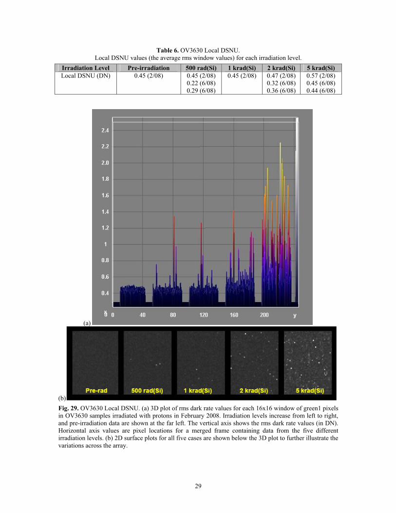
Table 6. OV3630 Local DSNU. Local DSNU values (the average rms window values) for each irradiation level.
(a)
Irradiation Level Pre-irradiation 500 rad(Si) 1 krad(Si) 2 krad(Si) 5 krad(Si) Local DSNU (DN) 0.45 (2/08) 0.45 (2/08)
0.22 (6/08) 0.29 (6/08)
0.45 (2/08) 0.47 (2/08) 0.32 (6/08) 0.36 (6/08)
0.57 (2/08) 0.45 (6/08) 0.44 (6/08)
(b) Fig. 29. OV3630 Local DSNU. (a) 3D plot of rms dark rate values for each 16x16 window of green1 pixels in OV3630 samples irradiated with protons in February 2008. Irradiation levels increase from left to right, and pre-irradiation data are shown at the far left. The vertical axis shows the rms dark rate values (in DN). Horizontal axis values are pixel locations for a merged frame containing data from the five different irradiation levels. (b) 2D surface plots for all five cases are shown below the 3D plot to further illustrate the variations across the array.
29

8.1.3 Photo-Response Non-Uniformity (PRNU) PRNU was found to be very low for the OV3630. It was calculated as described in Section 7.1.4 and was ~1% at all radiation levels (Table 7).
Table 7. OV3630 PRNU.*
*The normalized photo responses used in our PRNU calculations have been corrected for dark signal.
Irradiation Level 500 rad(Si) 1 krad(Si) 2 krad(Si) 5 krad(Si) OV3630 PRNU
� over 160,000 pixels (2/08) � over 360,000 pixels (6/08)
(percentage of average) [~0.85 pre-irradiation]**
1.19 (2/08) 1.17 (6/08) 1.20 (6/08)
1.11 (2/08)
1.26 (2/08) 1.16 (6/08) 1.21 (6/08)
1.26 (2/08) 1.24 (6/08) 1.27 (6/08)
**Typical pre-irradiation value.
8.1.4 Pixel Noise Average rms pixel noise is shown in Figures 30 and 31. As with the Micron sensors, increases are seen with integration time and irradiation. Increases in noise with irradiation may be due to a combination of noise from increased dark current and random telegraph noise. Note that the scaling of the rms pixel noise in Figures 30 and 31 is in 1000ths of DN. Visually, this scaling gives the impression of decreased noise following irradiation to 500 rad(Si) and 1 krad(Si); however, the variations in the calculated values are actually very small. The noise is essentially unchanged at these levels.
0.202
0.204
0.206
0.208
0.210
0.212
0.214
0.216
0.218
0.220
0 50 100 150 200 250 300 350 400 450
Integration Time (msec)
rms
pixe
l noi
se (D
N) Pre-irradiation
500 rad(Si)1 krad(Si)2 krad(Si)5 krad(Si)
Fig. 30. Average rms pixel noise for the OV3630 samples irradiated during the February 2008 proton test. Increases in noise with irradiation may be due to a combination of noise from increased dark current and random telegraph noise.
30
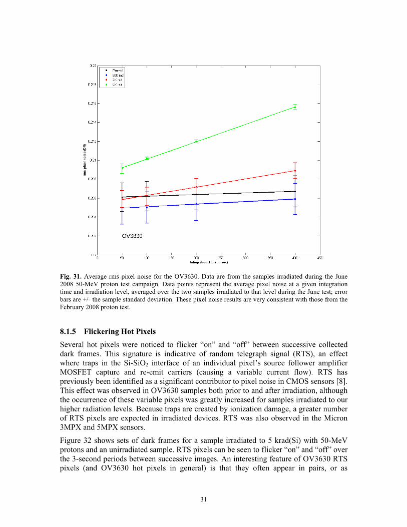
Fig. 31. Average rms pixel noise for the OV3630. Data are from the samples irradiated during the June 2008 50-MeV proton test campaign. Data points represent the average pixel noise at a given integration time and irradiation level, averaged over the two samples irradiated to that level during the June test; error bars are +/- the sample standard deviation. These pixel noise results are very consistent with those from the February 2008 proton test.
8.1.5 Flickering Hot Pixels Several hot pixels were noticed to flicker “on” and “off” between successive collected dark frames. This signature is indicative of random telegraph signal (RTS), an effect where traps in the Si-SiO2 interface of an individual pixel’s source follower amplifier MOSFET capture and re-emit carriers (causing a variable current flow). RTS has previously been identified as a significant contributor to pixel noise in CMOS sensors [8]. This effect was observed in OV3630 samples both prior to and after irradiation, although the occurrence of these variable pixels was greatly increased for samples irradiated to our higher radiation levels. Because traps are created by ionization damage, a greater number of RTS pixels are expected in irradiated devices. RTS was also observed in the Micron 3MPX and 5MPX sensors.
Figure 32 shows sets of dark frames for a sample irradiated to 5 krad(Si) with 50-MeV protons and an unirradiated sample. RTS pixels can be seen to flicker “on” and “off” over the 3-second periods between successive images. An interesting feature of OV3630 RTS pixels (and OV3630 hot pixels in general) is that they often appear in pairs, or as
31
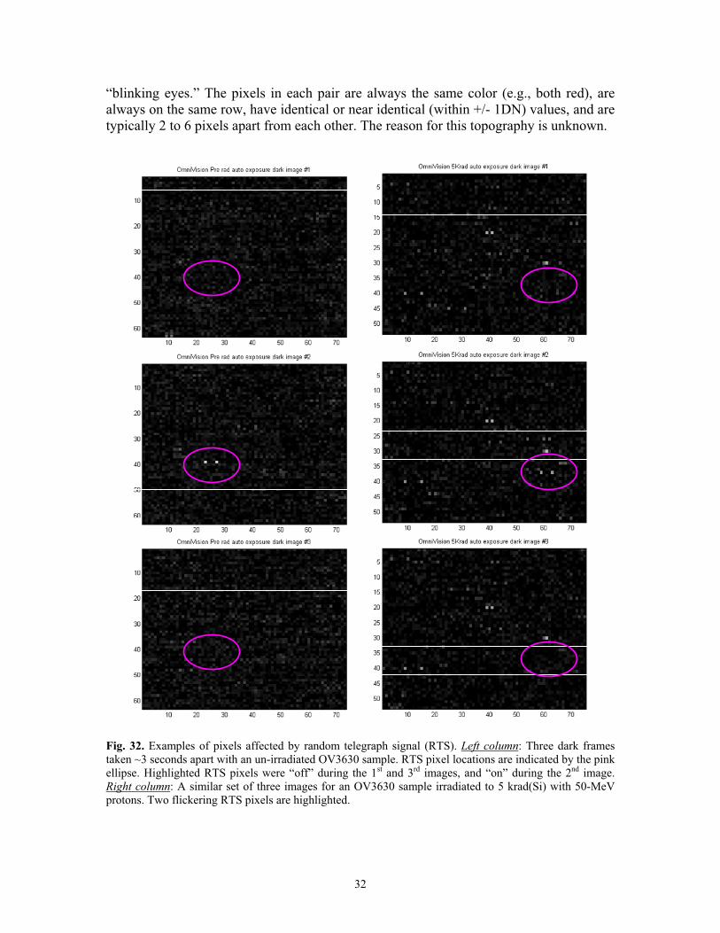
“blinking eyes.” The pixels in each pair are always the same color (e.g., both red), are always on the same row, have identical or near identical (within +/- 1DN) values, and are typically 2 to 6 pixels apart from each other. The reason for this topography is unknown.
Fig. 32. Examples of pixels affected by random telegraph signal (RTS). Left column: Three dark frames taken ~3 seconds apart with an un-irradiated OV3630 sample. RTS pixel locations are indicated by the pink ellipse. Highlighted RTS pixels were “off” during the 1st and 3rd images, and “on” during the 2nd image. Right column: A similar set of three images for an OV3630 sample irradiated to 5 krad(Si) with 50-MeV protons. Two flickering RTS pixels are highlighted.
32
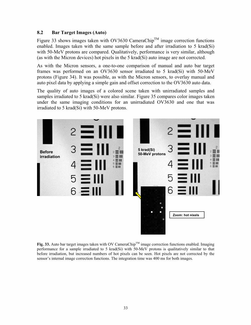
8.2 Bar Target Images (Auto) Figure 33 shows images taken with OV3630 CameraChipTM image correction functions enabled. Images taken with the same sample before and after irradiation to 5 krad(Si) with 50-MeV protons are compared. Qualitatively, performance is very similar, although (as with the Micron devices) hot pixels in the 5 krad(Si) auto image are not corrected.
As with the Micron sensors, a one-to-one comparison of manual and auto bar target frames was performed on an OV3630 sensor irradiated to 5 krad(Si) with 50-MeV protons (Figure 34). It was possible, as with the Micron sensors, to overlay manual and auto pixel data by applying a simple gain and offset correction to the OV3630 auto data.
The quality of auto images of a colored scene taken with unirradiated samples and samples irradiated to 5 krad(Si) were also similar. Figure 35 compares color images taken under the same imaging conditions for an unirradiated OV3630 and one that was irradiated to 5 krad(Si) with 50-MeV protons.
Fig. 33. Auto bar target images taken with OV CameraChipTM image correction functions enabled. Imaging performance for a sample irradiated to 5 krad(Si) with 50-MeV protons is qualitatively similar to that before irradiation, but increased numbers of hot pixels can be seen. Hot pixels are not corrected by the sensor’s internal image correction functions. The integration time was 400 ms for both images.
Zoom: hot pixels
Before irradiation
5 krad(Si)50-MeV protons
33

Fig. 34. Comparison of manual and auto green1 pixel data on the same row of an OV3630 sample irradiated to 5 krad(Si) with 50-MeV protons. The data can be overlaid by correcting for gain and a simple offset shift.
Fig. 35. Comparison of color images collected with an unirradiated OV3630 sensor and one that has been irradiated to 5 krad(Si) with 50-MeV protons. The images were collected with auto correction functions enabled, and are qualitatively very similar.
34

35
9.0 Conclusions and Next Steps Our selected Micron and OmniVision commercial CMOS sensors have all shown encouraging performance following unbiased proton irradiation to 5 krad(Si), and powered irradiation to 5 krad(Si) with Co-60. Although the higher dark rate pixels (“hot pixels”) created by the proton irradiations would not be correctable without using additional image correction strategies (such as the use of a shutter to allow the collection of dark frames for hot pixel mapping), the uncorrected presence of these pixels would not be expected to significantly impact image quality for an outreach or survey camera application.
In late FY08, we were informed by OmniVision that they will no longer be offering the OV3630 sensor. An alternative product, the newer OV3640, was recommended for future procurements. However, the OV3630 and OV3640 do not have identical features; they differ both in pixel size and available on-chip functions. This raised a concern regarding longevity expectations for potential flight commercial sensors. It is recommended that continued FY09 commercial sensor study begin with investigation of the expected longevity of past and future commercial sensors tested under NEPP. It is also recommended that the survey be broadened in FY09 to include testing of additional commercial sensors that would be suitable for outreach, survey camera, or other applications.
10.0 References [1] Becker, H.N., Alexander, J.W., Thorbourn, D.O., and Konefat, E.H.,
“Commercial Sensor Survey Status Report,” JPL Publication 08-8. February 2008.
[2] Micron Technology, Inc. “MT9P031 1/2.5-inch, 5-Mp CMOS Image Sensor,” Limited Data Sheet, © 2006. http://download.micron.com/pdf/product_brief/MT9P031_5100_PB.pdf. 13 July 2007.
[3] Micron Technology, Inc. “MT9T031 1/2-inch, 3-Mp CMOS Image Sensor,” Limited Data Sheet, © 2006. http://download.micron.com/pdf/product_brief/MT9T031_3100_PB.pdf. 13 July 2007.
[4] OmniVision. “OV3630 3.2 MPixel product brief.” http://www.ovt.com/data/parts/pdf/Brief3630V2.1.pdf, 13 July 2007.
[5] OmniVision. “Support/Evaluation Modules.” http://www.ovt.com/support/evalkits.asp. Accessed 25 March 2008.
[6] Pickel, J.C., Kalma, A.H., Hopkinson, G.R., and Marshall, C.J., “Radiation Effects on Photonic Imagers – A Historical Perspective,” IEEE Trans. Nucl. Sci., vol. 50, no. 3, pp. 671–688, June 2003.
[7] OmniVision. “OV5620 5.17 MPixel product brief.” http://www.ovt.com/data/parts/pdf/Brief5620V4.2.pdf. 13 July 2007.
[8] Janesick, J., et al., “Fundamental performance differences between CMOS and CCD imagers; Part 1,” Proc. of SPIE, Vol. 6276, High Energy, Optical, and Infrared Detectors for Astronomy II. 15 June 2006.
11.0 Appendix 1 – Sensor Selection Criteria [1] The survey for candidate test sensors focused primarily on low-cost (from a few tens of dollars to a few hundred dollars per sensor), low-power, commercial CMOS sensor products, such as those used in cell phones, webcams, or consumer-grade digital still cameras. Only inexpensive, commercial imagers with potential for use in low-duty-cycle space exploration applications were considered; the task does not address high-cost science grade imagers or hardened technologies. Charge coupled devices (CCDs) are typically at least an order of magnitude higher in cost than their CMOS counterparts, and they also require more complicated support circuitry to evaluate. Therefore, we did not put emphasis on CCDs in the FY07 candidate survey. Cameras for outreach programs or low-cost surveys should be relatively inexpensive to both build and host on a spacecraft and, ideally, they should be small in size. Limitations on telemetry bandwidths, power, mass, and requirements on spacecraft real estate are key considerations that helped to guide the choice of which sensors to target. Small bandwidths suggest that large arrays with as many as 14 Megapixels (Mpixel) may not be practical for the applications we are considering. In fact, many space missions have successfully used 0.5- to 2-Mpixel monochromatic CCD cameras with filter wheels to provide excellent images. However, filter wheels add expense and also significant mass, so the choice of color detectors with 1 to 5 Mpixel (which can provide similar color resolution) presents a reasonable compromise. Optics are an additional camera cost driver, so it is important to keep them small when designing an inexpensive camera. Common small detector optical formats are 1/4, 1/3, 1/2.5, and 1/2 inch. For a fixed set of optics, decreasing the pixel size can increase resolution, but it also decreases the amount of signal charge that an individual pixel can collect, which reduces dynamic range. Note that the photosensitive active area of pixels, the portion of which is described as “fill factor,” is further reduced in CMOS sensors due to the presence of circuitry within the individual pixels. This problem is mitigated in some sensor designs by the use of microlenses. Microlenses are small lenses that are placed directly on top of the pixels to focus light into the photosensitive region of the pixel. Our trades led us to consider pixels widths between ~2 and 8 microns (μm), array sizes of ~1 to 6 Mpixel, color arrays, and 1/4- to 1/2-inch optical formats. Candidates also had to be available as packaged parts, not bare die. The major criteria for selection were:
(1) Low cost. (2) Sensor format, geared toward suitability for the applications mentioned above. (3) Relative ease of evaluation (with the goal to minimize test development costs): A
manufacturer-endorsed evaluation kit had to be available for the sensor line, and the kit was required to have the potential to easily adapt to the logistics of incremental dose testing on multiple samples. Our requirements also included the ability of the evaluation kit to produce RAW format images and provide direct control over a few select parameters, such as integration time.
36

REPORT DOCUMENTATION PAGE Form Approved OMB No. 0704-0188
The public reporting burden for this collection of information is estimated to average 1 hour per response, including the time for reviewing instructions, searching existing data sources, gathering and maintaining the data needed, and completing and reviewing the collection of information. Send comments regarding this burden estimate or any other aspect of this collection of information, including suggestions for reducing this burden, to Department of Defense, Washington Headquarters Services, Directorate for Information Operations and Reports (0704-0188), 1215 Jefferson Davis Highway, Suite 1204, Arlington, VA 22202-4302. Respondents should be aware that notwithstanding any other provision of law, no person shall be subject to any penalty for failing to comply with a collection of information if it does not display a currently valid OMB control number. PLEASE DO NOT RETURN YOUR FORM TO THE ABOVE ADDRESS.1. REPORT DATE (DD-MM-YYYY) 00-10-2008
2. REPORT TYPE JPL Publication
3. DATES COVERED (From - To) N/A
5a. CONTRACT NUMBER NAS7-03001 5b. GRANT NUMBER
4. TITLE AND SUBTITLE Commercial Sensor Survey Fiscal Year 2008 Compendium Radiation Test Report
5c. PROGRAM ELEMENT NUMBER 5d. PROJECT NUMBER 102197 5e. TASK NUMBER 3.21.4
6. AUTHOR(S) Becker, Heidi N.; Dolphin, Michael D.; Thorbourn, Dennis O.; Alexander, James W.; Salomon, Phil M.
5f. WORK UNIT NUMBER
7. PERFORMING ORGANIZATION NAME(S) AND ADDRESS(ES) Jet Propulsion Laboratory California Institute of Technology 4800 Oak Grove Drive Pasadena, CA 91009
8. PERFORMING ORGANIZATION REPORT NUMBER JPL Publication 08-26
10. SPONSORING/MONITOR'S ACRONYM(S) NASA/NEPP
9. SPONSORING/MONITORING AGENCY NAME(S) AND ADDRESS(ES) National Aeronautics and Space Administration Washington, DC 20546-0001 11. SPONSORING/MONITORING
REPORT NUMBER
12. DISTRIBUTION/AVAILABILITY STATEMENT Unclassified—Unlimited Subject Category 35 Instrumentation and Photography, 93 Space Radiation
Availability: NASA CASI (301) 621-0390 Distribution: Nonstandard 13. SUPPLEMENTARY NOTES
14. ABSTRACT The NASA Electronic Parts and Packaging (NEPP) Program Sensor Technology Commercial Sensor Survey task is geared toward benefiting future NASA space missions with low-cost, short-duty-cycle, visible-wavelength imaging needs. Such applications could include imaging for educational outreach purposes or short surveys of spacecraft, planetary, or lunar surfaces. Under the task, inexpensive commercial grade CMOS sensors were surveyed in fiscal year 2007 (FY07) and three sensors were selected for total ionizing dose (TID) and displacement damage dose (DDD) tolerance testing. The selected sensors had to meet selection criteria chosen to support small, low-mass cameras that produce good resolution color images. This compendium provides results for all radiation testing performed in FY08 on the Micron and OmniVision sensors that were selected in FY07 for radiation tolerance testing.
15. SUBJECT TERMS sensors, space radiation, cameras
16. SECURITY CLASSIFICATION OF: 19a. NAME OF RESPONSIBLE PERSON STI Help Desk at [email protected] a. REPORT
U b. ABSTRACT U
c. THIS PAGE U
17. LIMITATION OF ABSTRACT UU
18. NUMBER OF PAGES 42 19b. TELEPHONE NUMBER (Include area code)
(301) 621-0390
JPL 2659 R 10 / 03 W Standard Form 298 (Rev. 8-98) Prescribed by ANSI Std. Z39-18
Related Documents


