Comments on Lab #4 Annotating Timing Diagrams • Draw viewer’s attention to the points you are trying to show / verify – Important output states • glitch or no glitch here • Particular result you expected or wanted to verify – Events that caused important outcomes • Which input conditions (important “test vectors”)?

Comments on Lab #4 Annotating Timing Diagrams Draw viewer’s attention to the points you are trying to show / verify –Important output states glitch or.
Dec 31, 2015
Welcome message from author
This document is posted to help you gain knowledge. Please leave a comment to let me know what you think about it! Share it to your friends and learn new things together.
Transcript

Comments on Lab #4
Annotating Timing Diagrams
• Draw viewer’s attention to the points you are trying to show / verify– Important output states
• glitch or no glitch here
• Particular result you expected or wanted to verify
– Events that caused important outcomes• Which input conditions (important “test vectors”)?

Comments on Lab #4
Annotating Timing Diagrams• Draw viewer’s attention to the points you
are trying to show / verify USING:– Causal arrows annotation– Circle or highlight– Add notes with arrows pointing to where you
see it in diagram– (Your own ideas to CLEARLY &
OBVIOUSLY point things out.)

Experiment 5 Procedure Overview
• Analyze “unknown” circuit using a Logic Analyzer
• Design and Implement an equivalent function on Nexys board using VHDL

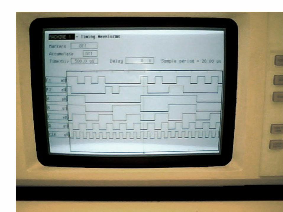
Logic Analyzer
• Tool to debug an actual digital circuit• Actual circuits seldom initially work as expected• LA output is primarily a timing diagram that
displays the states of designated signals in a circuit.
Examples: Last week’s experiment and this one:– Exp 4: Timing Diagram from Simulation (B2 Spice)– Exp 5: Timing Diagram from Physical Circuit (LA)
Timing Diagram from Simulation (ModelSim)
SORRY!“That’s life” in
the “real” world!!

Logic Analyzer Operation
• LA takes “snapshots” (samples) of circuit conditions at certain intervals.
• Interpolates sample points to produce timing diagram
• Complete example provided in Experiment 5 introduction

The Trigger
• The trigger is a description of the circuit conditions you intend on viewing.
• Logic Analyzer fills and updates half of storage memory while waiting for the trigger event– Filled with data that occurs before the trigger.
• The other half of the storage memory is filled with sample points that occur after the trigger conditions are met

Example of LA Operation
datat0
datat1
datat2
datat15
datat16
datat17
datat18
datat19
datat7
datat6
datat2
datat1
datat0
datat3
datat4
datat5
datat10
datat9
datat8
Trigger Found!

Connecting Logic Analyzer
Wire ConnectionsYOU must make

Nexys BoardJA
JB
JC
1
2
3
4
5
6

Nexys-2 Board

Xilinx Design Methodology
• The steps required in order to model, simulate and implement a circuit using the Xilinx ISE software
• Basic steps are as simple or as complicated as you want to make them
• Xilinx ISE and VHDL used again in CPE 229/269/329 and CSC 315
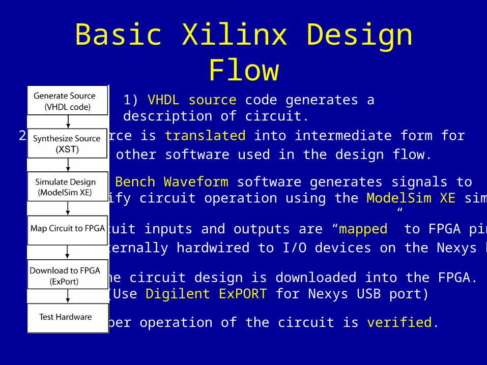
Basic Xilinx Design Flow
1) VHDL source code generates a description of circuit.
2) VHDL source is translated into intermediate form for
use by other software used in the design flow.
3) Test Bench Waveform software generates signals to verify circuit operation using the ModelSim XE simulator.
4) Circuit inputs and outputs are “mapped” to FPGA pins
externally hardwired to I/O devices on the Nexys board.
5) The circuit design is downloaded into the FPGA. (Use Digilent ExPORT for Nexys USB port)
6) Proper operation of the circuit is verified.

Create a New VHDL Source Module & Define Inputs/Outputs

Insert code here
Add your logic expression to the VHDL code module template
Your definition of input / output signals is turned into a VHDL “Entity”


You have to resize this window to see the results


Use the marker to check the truth table

Experiment 5 - Procedure Steps1. Connect the Nexys board to the LA interface (wires)2. Setup the Logic Analyzer (display, trigger, etc.)3. Download the test file to Nexys4. Use the logic analyzer to obtain the Timing Waveform.5. From that waveform, generate the Truth Table
(2 functions)
6. Perform a K-Map reduction7. Write out the logic equation for your truth table for VHDL
coding (Compact minterm, reduced SOP)8. Create a VHDL project, using the process in the Exp 5
Procedures.9. Add your 2 functions to the VHDL source code file.10. Use the Xilinx tools to compile the code & synthesize a
circuit.11. Verify the circuit using the ModelSim simulator12. Download the .bit file and manually verify your solution.

A Little “Sage Advice”
• Since this is your first time using the tools, be Since this is your first time using the tools, be sure to follow sure to follow allall of the steps, in the order of the steps, in the order given. given. – Skipping steps may result inSkipping steps may result in
horrendouslyhorrendously hideoushideous outcomes outcomes that you that you reallyreally don’t want to experience. don’t want to experience.
– A confused CAD tool is not a happy CAD tool!A confused CAD tool is not a happy CAD tool! ; ;((
• Be sure to read the Be sure to read the ExplanationsExplanations as you as you proceed, so that you begin to understand proceed, so that you begin to understand whywhy you are doing what you are doingyou are doing what you are doing.

FOR NEXT WEEK
• Be sure to read ahead and understand the entire Lab Procedure & Background– Especially the operation of the 2 devices you
need to design
• Bring a draft of the VHDL code for your BCD-to-7segment Decoder with you to Lab– Design AHEAD OF TIME
…or you probably won’t finish!!– Use text editor, Xilinx ISE tools or hand write

So, for today… “Go for it!...”
See what happens…Ask questions when things
don’t make sense!
WORK QUICKLY!!…and have fun!

Related Documents