NANO EXPRESS Open Access Combining scanning probe microscopy and x-ray spectroscopy Carole Fauquet 1* , Maël Dehlinger 1 , Franck Jandard 1 , Sylvain Ferrero 2 , Daniel Pailharey 2 , Sylvia Larcheri 3 , Roberto Graziola 3 , Juris Purans 4 , Aniouar Bjeoumikhov 5 , Alexei Erko 6 , Ivo Zizak 6 , Brahim Dahmani 7 and Didier Tonneau 1 Abstract A new versatile tool, combining Shear Force Microscopy and X-Ray Spectroscopy was designed and constructed to obtain simultaneously surface topography and chemical mapping. Using a sharp optical fiber as microscope probe, it is possible to collect locally the visible luminescence of the sample. Results of tests on ZnO and on ZnWO 4 thin layers are in perfect agreement with that obtained with other conventional techniques. Twin images obtained by simultaneous acquisition in near field of surface topography and of local visible light emitted by the sample under X-Ray irradiation in synchrotron environment are shown. Replacing the optical fibre by an X-ray capillary, it is possible to collect local X-ray fluorescence of the sample. Preliminary results on Co-Ti sample analysis are presented. Introduction Non destructive tools providing elemental and chemical analysis at high lateral resolution are needed for life and physical sciences. For example electronics or glass industries need sub-100 nm resolution tools for material processing and control (RRAM, FeRAM, smart materi- als, solar cells) [1]. During the last ten years, numbers of characterization tools were thus developed to obtain with the same apparatus sample imaging and chemical mapping. For example TEM (Transmission Electron Microscopy) is combined with EELS (Electron Energy Loss Spectroscopy) techniques to study oxidation states in transition metal oxides [2]. Near Field Microscopes are powerful tools for surface topography and analysis at nanometric lateral resolution. These equipments allow various in-situ spectroscopies, to probe surface local magnetic properties [3], electronic states [4] or even to identify and localize specific chemical group on very small features [5]. Combination of equipments can give further insights in sample analysis as, e.g. a combination of PEEM with STM [6]. However, those techniques are not simultaneously performed, so that authors had to mark the surface to recover the PEEM analysis localiza- tion for STM imaging at the same place. Conventional X-Ray Absorption Spectroscopies are fine analysis techniques providing chemical and struc- tural properties of a material, based on the spectroscopy of the emitted photons or photoelectrons. They require a high brightness X-Ray excitation source, usually a syn- chrotron beam, to irradiate the sample. Emergent high resolution microscopies take advantage of X-ray analysis to perform chemical mapping on samples [7]. For exam- ple, STXM (Scanning Transmission X-Ray Microscope) in transmission mode [7] and XPEEM (X-ray Photoe- mission Electron Microscopy) enable to obtain a sample chemical contrast and electronic structure from indivi- dual nanostructures [8,9]. Coupling X-Ray Spectroscopy and Scanning Probe Microscopy allows collecting with the microscope probe, the sample emission (electron, photons) under X- ray excitation, leading to surface topography and chemi- cal mapping at high resolution at the same place. This concept is now widely investigated in synchrotron envir- onment [10-13]. In this work, we present a versatile Shear Force Microscope head, which can be coupled to an X-ray beam illuminating the sample just at the level of micro- scope probe apex. This microscope has been fitted to a * Correspondence: [email protected] 1 Université de la Méditerranée, CNRS-CINaM, Faculté des Sciences de Luminy, case 913, 13288 Marseille cedex 09, France Full list of author information is available at the end of the article Fauquet et al. Nanoscale Research Letters 2011, 6:308 http://www.nanoscalereslett.com/content/6/1/308 © 2011 Fauquet et al; licensee Springer. This is an Open Access article distributed under the terms of the Creative Commons Attribution License (http://creativecommons.org/licenses/by/2.0), which permits unrestricted use, distribution, and reproduction in any medium, provided the original work is properly cited.

Welcome message from author
This document is posted to help you gain knowledge. Please leave a comment to let me know what you think about it! Share it to your friends and learn new things together.
Transcript

NANO EXPRESS Open Access
Combining scanning probe microscopy and x-rayspectroscopyCarole Fauquet1*, Maël Dehlinger1, Franck Jandard1, Sylvain Ferrero2, Daniel Pailharey2, Sylvia Larcheri3,Roberto Graziola3, Juris Purans4, Aniouar Bjeoumikhov5, Alexei Erko6, Ivo Zizak6, Brahim Dahmani7 andDidier Tonneau1
Abstract
A new versatile tool, combining Shear Force Microscopy and X-Ray Spectroscopy was designed and constructed toobtain simultaneously surface topography and chemical mapping. Using a sharp optical fiber as microscope probe,it is possible to collect locally the visible luminescence of the sample. Results of tests on ZnO and on ZnWO4 thinlayers are in perfect agreement with that obtained with other conventional techniques. Twin images obtained bysimultaneous acquisition in near field of surface topography and of local visible light emitted by the sample underX-Ray irradiation in synchrotron environment are shown. Replacing the optical fibre by an X-ray capillary, it ispossible to collect local X-ray fluorescence of the sample. Preliminary results on Co-Ti sample analysis arepresented.
IntroductionNon destructive tools providing elemental and chemicalanalysis at high lateral resolution are needed for life andphysical sciences. For example electronics or glassindustries need sub-100 nm resolution tools for materialprocessing and control (RRAM, FeRAM, smart materi-als, solar cells) [1]. During the last ten years, numbers ofcharacterization tools were thus developed to obtainwith the same apparatus sample imaging and chemicalmapping. For example TEM (Transmission ElectronMicroscopy) is combined with EELS (Electron EnergyLoss Spectroscopy) techniques to study oxidation statesin transition metal oxides [2]. Near Field Microscopesare powerful tools for surface topography and analysis atnanometric lateral resolution. These equipments allowvarious in-situ spectroscopies, to probe surface localmagnetic properties [3], electronic states [4] or even toidentify and localize specific chemical group on verysmall features [5]. Combination of equipments can givefurther insights in sample analysis as, e.g. a combinationof PEEM with STM [6]. However, those techniques arenot simultaneously performed, so that authors had to
mark the surface to recover the PEEM analysis localiza-tion for STM imaging at the same place.Conventional X-Ray Absorption Spectroscopies are
fine analysis techniques providing chemical and struc-tural properties of a material, based on the spectroscopyof the emitted photons or photoelectrons. They requirea high brightness X-Ray excitation source, usually a syn-chrotron beam, to irradiate the sample. Emergent highresolution microscopies take advantage of X-ray analysisto perform chemical mapping on samples [7]. For exam-ple, STXM (Scanning Transmission X-Ray Microscope)in transmission mode [7] and XPEEM (X-ray Photoe-mission Electron Microscopy) enable to obtain a samplechemical contrast and electronic structure from indivi-dual nanostructures [8,9].Coupling X-Ray Spectroscopy and Scanning Probe
Microscopy allows collecting with the microscopeprobe, the sample emission (electron, photons) under X-ray excitation, leading to surface topography and chemi-cal mapping at high resolution at the same place. Thisconcept is now widely investigated in synchrotron envir-onment [10-13].In this work, we present a versatile Shear Force
Microscope head, which can be coupled to an X-raybeam illuminating the sample just at the level of micro-scope probe apex. This microscope has been fitted to a
* Correspondence: [email protected]é de la Méditerranée, CNRS-CINaM, Faculté des Sciences deLuminy, case 913, 13288 Marseille cedex 09, FranceFull list of author information is available at the end of the article
Fauquet et al. Nanoscale Research Letters 2011, 6:308http://www.nanoscalereslett.com/content/6/1/308
© 2011 Fauquet et al; licensee Springer. This is an Open Access article distributed under the terms of the Creative CommonsAttribution License (http://creativecommons.org/licenses/by/2.0), which permits unrestricted use, distribution, and reproduction inany medium, provided the original work is properly cited.

synchrotron beam line, to simultaneously performXAFS-XEOL (X Ray Absorption Fine Structure - X RayExcited Optical Luminescence) spectroscopy, and sur-face topography. A sharp optical fiber is used as micro-scope tip for sample topography and for local samplevisible luminescence collection. Spectra exhibit the var-iation of the visible light intensity as a function of inci-dent primary beam energy. As an absorption threshold,characteristic of an emitting element present in thematerial is crossed, the intensity of the visible light dras-tically increases and is followed by oscillations linked tothe atomic environment and structure of this element[14]. Chemical mapping was achieved on ZnO andZnWO4 - ZnO samples. μ-XRF (micro X-Ray Fluores-cence) analysis was successfully carried out on Co-Tisamples, replacing the optical fibre, microscope probe,by a thin X-ray capillary and using a rotating anode (CuKa) as excitation source.
ResultsInstrumentationThe apparatus consists in an home-made shear-forcemicroscope (see Figure 1) whose probe is a sharp Alu-minium-coated optical fibre (aperture 50 nm) thatlocally collects the visible light emitted by the sampleilluminated by X-Ray radiation (synchrotron environ-ment). The instrument, working in ambient conditionsor in liquid environment, allows simultaneous pixel bypixel surface topography measurement and chemicalmapping [15]. The analysed sample must fit with Scan-ning Probe Microscopy requirements (solid sample,roughness in the micronscale range). This apparatus isevaluated by characterization of ZnO and ZnWO4 -ZnO thin layers, exhibiting a high luminescence yield.The luminescence spectra are compared to thoseobtained in far field
This apparatus also enables the XRF signal local col-lection of the excited sample, replacing the device tun-ing fork-optical fibre by a fixed X-ray cylindricalcapillary (internal diameter 10 μm, length 50 mm). Thesample is excited by a rotating anode (excitation at con-stant energy, Cu Ka at 8 keV, power 40 kV × 40 mA)while the fluorescence signal is analyzed by EDX(Energy Dispersive X-ray). The excitation beam isfocused on the sample by a capillary lens (spot diameter20 μm) provided by IFG GmbH. The XRF technique isparticularly suitable for analysis of heavy elements, typi-cally heavier than sodium.
Nano-XAFS-XEOLIn Figure 2a we present the XAFS-XEOL spectrumobtained with the apparatus at ESRF ID03 line of a ZnOthin layer (~400 nm), prepared by Zn sputtering on asilicon substrate, followed by a 900°C annealing in air.The threshold, localized at 9664 eV, is characteristic ofvisible light emitted by Zn atoms after X-Ray absorp-tion. This spectrum is compared with that of the samesample (Figure 2b, bottom) and with that of a commer-cial stoichiometric ZnO powder sample for reference(Figure 2b, top, shifted), obtained in conventionalXAFS-XEOL spectroscopy, in far field, at the samebeamline. Spectra shown in Figure 2b are in very goodagreement in terms of both peak positions and relativemagnitudes measured with respect to the average signalabove threshold. This indicates that the ZnO sputteredlayer is stoichiometric. The great concordance betweenspectra Figure 2a and Figure 2b validates the instrumentconcept.A ZnWO4 - ZnO thin layer (~400 nm) was prepared
by co-sputtering Zn and W onto a silicon substrate, fol-lowed by a 900°C annealing in air. In Figure 3 we showtwin images corresponding to the simultaneous recordof both topography and luminescence cartography ofthe ZnWO4 - ZnO sample at various incident energies.In upper Figures 3-a, b, c, d the topography is pre-sented. Grains of 0.5 to more than 1μm are observed, aswas confirmed by conventional Atomic Force Micro-scopy. In Figures 3-e, f, g, h we present the correspond-ing luminescence cartography obtained respectively,from the left to the right, before and after the Zn-Kedge, as well as before and after the W-L edge. Images3a to 3 h contain 1024 × 1024 pixels. The remarkablestability of the instrument is noticeable, since it tookabout 8 h for recording this whole set of images. Image3 g, obtained at higher X-ray energy than the Zn thresh-old, also highlights Zn rich regions. The contrast islower than in Figure 3f since the acquisition is per-formed far from the maximum emission. Black zonescorrespond to non emitting or to grains emitting out ofthe fibre acceptance angle.
Quartz tuning fork
32KHz
Piezo ScannerX,Y,Z
“Shear force”Regulation
Optical fibre
XEOL signalLuminescence
Image
ImageTopography
ImageTopography
Synchrotron Beam
Figure 1 Principle of the home-built instrument. The instrumentcombines shear-force microscopy and XEOL spectroscopy.
Fauquet et al. Nanoscale Research Letters 2011, 6:308http://www.nanoscalereslett.com/content/6/1/308
Page 2 of 6

Post image processing can be carried out on Figure 3eto 3h to define ZnO and ZnWO4 rich areas. First, thepixel to pixel difference Figure 3f - Figure 3e (resp.Figure 3h - Figure 3g) gives the distribution of Zn (resp.W) luminescent sites. Then, to enhance the contrast,these two images are further converted in black andwhite scale. By this way we get two intermediate images,which are then used to obtain a chemical mapping of thelayer: the ZnO rich emitting areas can be obtained by dif-ference of these intermediate images (Figure 4a), sinceZn is present in both materials while W can be foundonly in ZnWO4 grains. Finally, a logic operation ‘AND’ isapplied between the intermediate images to highlight thedistribution of emitting ZnWO4 (Figure 4b) since Znmust be present in both materials. In fact a white pixel inFigure 4b is obtained only if the same pixel appearssimultaneously white on both intermediate images. Thisimage processing leads to a two-level (black and white)
image which increases significantly the contrast. SinceFigure 4a shows only few features, one can conclude theemitting centres are almost pure ZnWO4, as confirmedby XRD and micro-Raman analysis [16]. No obvious cor-relation with the topography is noticeable, since the emit-ting zones are not specifically centered in the grains.Collecting the XEOL signal in near field significantly
increases the lateral resolution of this technique, whichis now only limited by the aperture of the optical fibre.In fact, the resolution of the apparatus is limited by thetip curvature for topography (~100 nm) and by the opti-cal aperture for the light collection (~50 nm).
In-lab μ-XRF analysisReplacing the device tuning fork-optical fibre by a fixedX-ray cylindrical capillary the XRF collection conceptfeasibility is demonstrated on a test sample, composedof bulk Co and Ti juxtaposed sheets. The X-ray beam
(a) (b)
0,0
0,2
0,4
0,6
0,8
1,0
ID03 beamline
975097009650X-ray energy (eV)
Inte
nsity
(arb
.uni
ts)
975097009650X-ray energy (eV)
Inte
nsity
(arb
.uni
ts)
Inte
nsity
(arb
.uni
ts)
X-ray energy (eV)
Inte
nsity
(arb
.uni
ts)
X-ray energy (eV)
Inte
nsity
(arb
.uni
ts)
X-ray energy (eV)
ZnO film
Figure 2 XAFS-XEOL recorded spectra of - a: the sputtered ZnO film obtained in near-field; - b: the ZnO film (bottom) and of areference stoichiometric ZnO powder (top) by conventional technique. Spectra are expanded for clarity.
Fauquet et al. Nanoscale Research Letters 2011, 6:308http://www.nanoscalereslett.com/content/6/1/308
Page 3 of 6

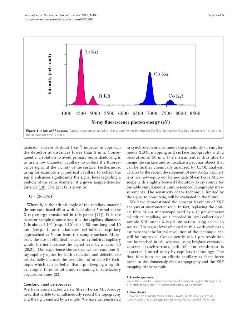
simultaneously illuminates both Co and Ti samples. Fig-ure 5 shows XRF spectra obtained using 10 μm diametercylindrical capillary approached at a distance of 5 mmfrom the sample surface. We obtain the Ka and Kbcharacteristic peaks of both Co and Ti, as reported inliterature [17]. Since the fluorescence yield of Co istwice that of Ti at excitation energy of 8 keV, the inci-dent spot might be slightly shifted on the titanium sheetregarding the Co-Ti separation.
With commonly marketed XRF equipment, withoutcapillary for detection, the lateral resolution is limitedby the diameter of the primary probe, in the range of 10μm. A resolution increase can be achieved by shrinkingdown the detector aperture. However, increasing theresolution from 10 to 1 μm, would lead to a factor lossof 100 on the signal. To reach the original signal level,the sample-detector distance must be drasticallydecreased. However the steric hindrance of the EDX
a9600 eV
b9666 eV
c10190 eV
d10207 eV
XEO
LTo
pogr
aphy
Figure 3 Twin topography-luminescence images. Top: (a-d) topography of a ZnO-ZnWO4 sputtered layer (2 × 2 μm2). Bottom: correspondingvisible light emission cartography under illumination by X-ray beam from left to right below (e) and above (f) the Zn-Ka threshold (9.6 keV) andbelow (g) and above (h) the W-L3threshold (10.2 keV). On top of the images is indicated the X-ray primary energy.
a bFigure 4 Zn (a) and W (b) rich emitting areas of a ZnO-ZnWO4 thin layer deposited by magnetron sputtering.
Fauquet et al. Nanoscale Research Letters 2011, 6:308http://www.nanoscalereslett.com/content/6/1/308
Page 4 of 6
detector (surface of about 1 cm2) impedes to approachthe detector at distances lower than 5 mm. Conse-quently, a solution to avoid primary beam shadowing isto use a low diameter capillary to collect the fluores-cence signal at the vicinity of the surface. Furthermore,using for example a cylindrical capillary to collect thesignal enhances significantly the signal level regarding apinhole of the same diameter at a given sample-detectordistance [18]. The gain G is given by:
G =(2θcD/d
)2
Where θc is the critical angle of the capillary material(in our case fused silica with θc of about 5 mrad at theX-ray energy considered in this paper [19]), D is thedetector-sample distance and d is the capillary diameter.G is about 3.103 (resp. 3.105) for a 50 mm long and 10μm (resp. 1 μm) diameter cylindrical capillaryapproached at 5 mm from the sample surface. More-over, the use of elliptical instead of cylindrical capillarywould further increase the signal level by a factor 20[20,21]. Our experience shows that we can combine X-ray capillary optics for both excitation and detection tosubstantially increase the resolution of in-lab XRF tech-nique which can be better than 1μm keeping a signifi-cant signal to noise ratio and remaining in satisfactoryacquisition times [22].
Conclusion and perspectivesWe have constructed a new Shear-Force Microscopyhead that is able to simultaneously record the topographyand the light emitted by a sample. We have demonstrated
in synchrotron environment the possibility of simulta-neous XEOL mapping and surface topography with aresolution of 50 nm. The instrument is thus able toimage the surface and to localize a peculiar object thatcan be further chemically analyzed by XEOL analysis.Thanks to the recent development of new X-Ray capillarylens, we now equip our home-made Shear Force Micro-scope with a tightly focused laboratory X-ray source foron-table simultaneous Luminescence-Topography mea-surements. The sensitivity of the technique, limited bythe signal to noise ratio, will be evaluated in the future.We have demonstrated the concept feasibility of XRF
analysis at micrometer scale. In fact, replacing the opti-cal fibre of our microscope head by a 10 μm diametercylindrical capillary, we succeeded in local collection ofsample XRF under X-ray illumination using an in-labsource. The signal level obtained in this work enables toestimate that the lateral resolution of the technique canstill be improved. Consequently sub-1 μm resolutioncan be reached in lab, whereas, using brighter excitationsources (synchrotron), sub-100 nm resolution isexpected, limited today by capillary technology. Thefinal idea is to use an elliptic capillary as shear forceprobe to simultaneously obtain topography and the XRFmapping of the sample.
AcknowledgementsThe authors thank European Community for financial support through FP6-XTIP strep project and FP7-Eureka-Eurostars LUMIX contracts.
Author details1Université de la Méditerranée, CNRS-CINaM, Faculté des Sciences deLuminy, case 913, 13288 Marseille cedex 09, France 2AXESS TECH, 750
Figure 5 In-lab μXRF spectra. Typical spectrum obtained on the sample when the frontier Co-Ti is illuminated. Capillary diameter is 10 μm andthe acquisition time is 100 s.
Fauquet et al. Nanoscale Research Letters 2011, 6:308http://www.nanoscalereslett.com/content/6/1/308
Page 5 of 6

Chemin de Beaupré, 13760 Saint Cannat, France 3Dipartimento di Fisica,Universita’ di Trento, Via Sommarive 14, 38123 Trento, Italy 4Latvian StateUniv, Inst Solid State Phys, LV-1063 Riga, Latvia 5IFG GmbH, RudowerChaussee 29/31, 12489 Berlin, Germany 6HZB-Synchrotron Bessy, AlbertEinstein Strasse, 15, 12489 Berlin, Germany 7LovaLite, 18 Rue A.Savary, 25000Besançon, France
Authors’ contributionsFJ, SF, DP and RG were involved in instrument design and fabrication; theyparticipated in conception and realization of light spectroscopy andmicroscopy experiments. DP and DT coordinated this study. BD wasinvolved in probe conception and light collection analysis. JP, SL and DTconceived the luminescence experiments and participated in interpretationof data. JP was at the concept origin of coupling scanning probemicroscopy and X-Ray spectroscopy. SL, CF and DT performed microscopydata and interpretation. MD, CF, AB and DT conceived the μ-XRFexperiments and participated in acquisition and interpretation of data. AB,AE and IZ were involved in μ-XRF data discussion and interpretation. CF, MDand DT drafted the manuscript. All authors read and approved the finalmanuscript.
Competing interestsPatent concerning the detection of XRF through capillary optics is pending(french patent n°1002392, 2010).
Received: 3 November 2010 Accepted: 7 April 2011Published: 7 April 2011
References1. International Technology Roadmap for Semiconductors, 2007 Edition,
Emerging Research Materials. [http://www.itrs.net/Links/2007ITRS/2007_Chapters/2007_ERM.pdf].
2. Varela M, Oxley MP, Luo W, Tao J, Watanabe M, Lupini AR, Pantelides ST,Pennycook SJ: Atomic-resolution imaging of oxidation states inmanganites. Phys Rev B 2009, 79: 085117.
3. Rugar D, Mamin HJ, Guethner P, Lambert SE, Stern JE, McFadyen I, Yogi T:Magnetic force microscopy: General principles and application tolongitudinal recording media. J Appl Phys 1990, 68: 1169.
4. Pietzsch O, Kubetzka A, Bode M, Wiesendanger R: Spin-Polarized ScanningTunneling Spectroscopy of Nanoscale Cobalt Islands on Cu(111). PhysRev Lett 2004, 92: 057202.
5. Duwez AS, Cuenot S, Jerome C, Rapino S, Zerbetto F: Mechanochemistry:targeted delivery of single molecules. NatureNanotechnology 2006, 1: 122.
6. Rohmer M, Wiemann C, Munzinger M, Guo L, Aeschlimann M, Bauer M:Local correlation of photoemission electron spectroscopy and STM at adefined cluster substrate system. Appl Phys A 2006, 82: 87.
7. Sakdinawat A, Attwood D: Nanoscale X-Ray imaging. Nat Photon 2010, 4:840.
8. Ratto F, Locatelli A, Fontana S, Kharrazi S, Ashtaputre S, Kulkarni SK, Heun S,Rosei F: Chemical Mapping of Individual Semiconductor Nanostructures.Small 2006, 3: 401.
9. Fraile Rodriguez A, Kleibert A, Bansmann J, Nolting F: Probing singlemagnetic nanoparticles by polarization-dependent soft x-ray absorptionspectromicroscopy. J Phys D: Appl Phys 2010, 43: 474006.
10. Ishii M: Capacitance X-ray absorption fine structure measurement usingscanning probe A new method for local structure analysis of surfacedefects. Physica B 2001, 308-310, 1153.
11. Schmid I, Raabe J, Quitmann C, Vranjkovic S, Hug HJ, Fink RH: NanoXAS, anovel concept for high resolution microscopy. J of Phys: Conference series2009, 186: 012015.
12. Pailharey D, Mathey Y, Jandard F, Larcheri S, Rocca F, Kuzmin A,Kalendarev R, Purans J, Dalba G, Graziola R, Dhez O: Nanoscale x-rayabsorption spectroscopy using XEOL-SNOM detection mode. Journal ofPhysics: Conference Series 2007, 93: 012038.
13. Eguchi T, Okuda T, Matsushima T, Kataoka A, Harasawa A, Akiyama K,Kinoshita T, Hasegawa Y: Element specific imaging by scanning tunnelingmicroscopy combined with synchrotron radiation light. Appl Phys Lett2006, 89: 243119.
14. Rogalev A, Goulon J: Chemical Applications of Synchrotron Radiation. InAdvanced Series in Physical Chemistry Part II: X-Rays and Applications. Volume12. Edited by: Sham TK. World Scientific, Singapore; 2002.
15. Larcheri S, Rocca F, Jandard F, Pailharey D, Grazaiola R, Kuzmin A, Purans J:X-ray excited optical luminescence detection by scanning near-fieldoptical microscope: A new tool for nanoscience. Review of ScientificInstruments 2008, 79: 1-9, 013702.
16. Larcheri S: Joint Use of X-ray synchrotron radiation microbeams and tipassisted photon detection for nano-scale XAFS spectroscopy andchemically sensitive surface mapping. PhD thesis Trento University (Italy);2007.
17. X-Ray Data Booklet, October 2009, Center for X-Ray Optics andAdvanced Light Source. Edited by: Lawrence Berkeley. National Laboratory,University of California; [http://cxro.lbl.gov/PDF/X-Ray-Data-Booklet.pdf].
18. Arkadiev V, Bjeoumikhov A: In Practical X-ray Fluorescence Analysis. Volume 3.Edited by: Beckhoff B, Kanngiesser B, Langhoff N, Wedell R, Wolff H.Springer-Verlag Berlin Heidelberg; 2006: 89-111.
19. Bjeoumikhov A, Bjeoumikhova S: In Modern Developments in X-ray andNeutron Optics, Springer series in Optical Sciences. Volume 137. Springer BerlinHeidelberg New York; 2008: 287-306.
20. Bjeoumikhov A, Bjeoumikhova S, Wedell R: Capillary Optics in X-rayAnalytics. Particle and Particle Systems Characterization 2006, 22: 384.
21. Bjeoumikhov A, Langhoff N, Bjeoumikhova S, Wedell R: Polycapillary Opticsfor micro-X-ray Fluorescence Analysis. Review of scientific Instrument 2005,76: 063115.
22. Tonneau D, Purans J, Fauquet C, Jandard F, Erko A, Bjeoumikhov A:Dispositif de caractérisation topographique et de cartographie chimiquede surfaces. French patent n°1002392 2010.
doi:10.1186/1556-276X-6-308Cite this article as: Fauquet et al.: Combining scanning probemicroscopy and x-ray spectroscopy. Nanoscale Research Letters 20116:308.
Submit your manuscript to a journal and benefi t from:
7 Convenient online submission
7 Rigorous peer review
7 Immediate publication on acceptance
7 Open access: articles freely available online
7 High visibility within the fi eld
7 Retaining the copyright to your article
Submit your next manuscript at 7 springeropen.com
Fauquet et al. Nanoscale Research Letters 2011, 6:308http://www.nanoscalereslett.com/content/6/1/308
Page 6 of 6
Related Documents