Combinatorial peel tests for the characterization of adhesion behavior of polymeric films * R. Song a,1 , M.Y.M. Chiang a, * , A.J. Crosby a,2 , A. Karim a , E.J. Amis a , N. Eidelman b a Polymer Division, National Institute of Standards and Technology, Gaithersburg, MD 20899, USA b Paffenbarger Research Center, American Dental Association Foundation, Gaithersburg, MD 20899, USA Received 16 November 2003; received in revised form 24 September 2004; accepted 5 October 2004 Available online 13 January 2005 Abstract The adhesion behavior of an optically smooth poly(methyl methacrylate) (PMMA) thin film (100 nm in thickness) on different evaporated metal substrates has been investigated using a combinatorial method approach. In this investigation through high-throughput peel tests, the relationship between annealing time, annealing temperature, surface energy, and ultraviolet degradation to the film adhesion has been examined. In addition, atomic force microscopy, optical microscopy and Fourier transform infrared microspectroscopy techniques have been adopted to elucidate the observations on the adhesion behavior from the peel tests. The results of this study demonstrate that the proposed combinatorial approach to characterize the dependence of adhesion on adhesion-controlling parameters has the potential to assess various factors affecting the adhesion. Published by Elsevier Ltd. Keywords: Combinatorial method; Adhesion; PMMA 1. Introduction Polymer adhesion is studied extensively because of important applications in industrial processes, such as composite manufacturing and durability, coatings, biome- dical devices and implants, and packaging for microelec- tronics components. Current (traditional) approaches to the characterization of adhesion have focused on attempts to isolate a single adhesion-controlling parameter and monitor the changes in adhesion with changes in that single parameter. However, this methodology is time consuming, discrete, and does not allow interplay between variables to be investigated. In this work, we present results of adhesion characterization for polymer/substrate systems using com- binatorial methodologies. The ultimate goals of this research are to develop techniques for processing and analyzing multi-variables of the interface and to map the dependence of adhesion on these adhesion-controlling parameters rapidly, practically, and efficiently. Recently, combinatorial methods have presented a paradigm for efficient polymer synthesis, characterization and curing. The revival of combinatorial methods within materials science has recently moved from inorganic [1–6] to organic and polymeric materials [7–21]. Several novel methods have emerged for the preparation of polymer film libraries with continuous gradients in temperature, compo- sition, thickness and surface energy, which make our current research available. From these libraries, several high- throughput screening methods have been demonstrated for cell–polymer interaction [14], polymer-blend phase beha- vior [15], block-copolymer segregation [16], and adhesion reliability [17–19,21]. Stimulated by the initial success in some fields of polymer characterization, we extend the combinatorial technique to polymer adhesion. In this study through peel tests, in which the force 0032-3861/$ - see front matter Published by Elsevier Ltd. doi:10.1016/j.polymer.2004.10.086 Polymer 46 (2005) 1643–1652 www.elsevier.com/locate/polymer * Official contribution of the National Institute of Standards and Technology; not subject to copyright in the United States. * Corresponding author. Tel.: C1 301 975 5186. E-mail address: [email protected] (M.Y.M. Chiang). 1 Present address: State Key Laboratory of Polymer Physics and Chemistry, Center of Molecular Science, Institute of Chemistry, Chinese Academy of Sciences, Beijing 100080, China. 2 Present address: Polymer Science and Engineering Department, University of Massachusetts, Amherst, MA 01003, USA.

Welcome message from author
This document is posted to help you gain knowledge. Please leave a comment to let me know what you think about it! Share it to your friends and learn new things together.
Transcript
Combinatorial peel tests for the characterization of adhesion behavior of
polymeric films*
R. Songa,1, M.Y.M. Chianga,*, A.J. Crosbya,2, A. Karima, E.J. Amisa, N. Eidelmanb
aPolymer Division, National Institute of Standards and Technology, Gaithersburg, MD 20899, USAbPaffenbarger Research Center, American Dental Association Foundation, Gaithersburg, MD 20899, USA
Received 16 November 2003; received in revised form 24 September 2004; accepted 5 October 2004
Available online 13 January 2005
Abstract
The adhesion behavior of an optically smooth poly(methyl methacrylate) (PMMA) thin film (100 nm in thickness) on different evaporated
metal substrates has been investigated using a combinatorial method approach. In this investigation through high-throughput peel tests, the
relationship between annealing time, annealing temperature, surface energy, and ultraviolet degradation to the film adhesion has been
examined. In addition, atomic force microscopy, optical microscopy and Fourier transform infrared microspectroscopy techniques have been
adopted to elucidate the observations on the adhesion behavior from the peel tests. The results of this study demonstrate that the proposed
combinatorial approach to characterize the dependence of adhesion on adhesion-controlling parameters has the potential to assess various
factors affecting the adhesion.
Published by Elsevier Ltd.
Keywords: Combinatorial method; Adhesion; PMMA
1. Introduction
Polymer adhesion is studied extensively because of
important applications in industrial processes, such as
composite manufacturing and durability, coatings, biome-
dical devices and implants, and packaging for microelec-
tronics components. Current (traditional) approaches to the
characterization of adhesion have focused on attempts to
isolate a single adhesion-controlling parameter and monitor
the changes in adhesion with changes in that single
parameter. However, this methodology is time consuming,
discrete, and does not allow interplay between variables to
be investigated. In this work, we present results of adhesion
0032-3861/$ - see front matter Published by Elsevier Ltd.
doi:10.1016/j.polymer.2004.10.086
* Official contribution of the National Institute of Standards and
Technology; not subject to copyright in the United States.
* Corresponding author. Tel.: C1 301 975 5186.
E-mail address: [email protected] (M.Y.M. Chiang).1 Present address: State Key Laboratory of Polymer Physics and
Chemistry, Center of Molecular Science, Institute of Chemistry, Chinese
Academy of Sciences, Beijing 100080, China.2 Present address: Polymer Science and Engineering Department,
University of Massachusetts, Amherst, MA 01003, USA.
characterization for polymer/substrate systems using com-
binatorial methodologies. The ultimate goals of this
research are to develop techniques for processing and
analyzing multi-variables of the interface and to map the
dependence of adhesion on these adhesion-controlling
parameters rapidly, practically, and efficiently.
Recently, combinatorial methods have presented a
paradigm for efficient polymer synthesis, characterization
and curing. The revival of combinatorial methods within
materials science has recently moved from inorganic [1–6]
to organic and polymeric materials [7–21]. Several novel
methods have emerged for the preparation of polymer film
libraries with continuous gradients in temperature, compo-
sition, thickness and surface energy, which make our current
research available. From these libraries, several high-
throughput screening methods have been demonstrated for
cell–polymer interaction [14], polymer-blend phase beha-
vior [15], block-copolymer segregation [16], and adhesion
reliability [17–19,21]. Stimulated by the initial success in
some fields of polymer characterization, we extend the
combinatorial technique to polymer adhesion.
In this study through peel tests, in which the force
Polymer 46 (2005) 1643–1652
www.elsevier.com/locate/polymer
R. Song et al. / Polymer 46 (2005) 1643–16521644
required to peel a test film from a test substrate is recorded
and gives a measure of adhesion (the peel energy for
debonding the film from the substrate), we present a high-
throughput (combinatorial) approach to study the effects of
polymer annealing temperature and time on adhesion
development for different substrates. Also, the relationship
between the annealing time, annealing temperature, surface
energy, and ultraviolet (UV) degradation to the film
adhesion has been examined using the combinatorial
approach. Poly (methyl methacrylate) (PMMA) has been
selected as the subject polymer, since it can be easily
prepared into a uniform thin film and is relatively stable
upon heating. Silicon, aluminum, chromium, copper and
gold have been used as the substrate.
2. Materials and experiments3
2.1. Film samples and substrate preparation
The PMMA sample (from Polysciences, Inc, Warring-
ton, PA, USA) used in this study has a molar mass and
polydispersity of 100,000 g/mol and 2.26, respectively.
Preliminary test indicated that it has a glass transition
temperature (Tg) of ca. 105 8C (probed by differential
scanning calorimeter (DSC) with a heating rate of
20 8C/min). The PMMA solution in chloroform (5% by
mass fraction) was spin-coated on a silicon substrate at
4 rad/s for 30 s to form a PMMA film (ca. 100 nm in
thickness) on a silicon substrate. The resulting film was
removed from the substrate by floating in water and
transferred to a selected substrate. By using this process,
the bonding strength of such film on a substrate can be
evaluated by a peel test at the early stages of annealing since
the interfacial strength is relatively low.
In this study, PMMA films were placed on silicon wafers
(Polishing Corporation of American, CA) and on silicon
wafers coated with thin metal layers of Au, Al, Cr, and Co,
to mimic different substrates such that their effects on the
adhesion can be investigated. These metal layers were
deposited on the silicon wafer using a thermal evaporator
(Granville-Phillips Company, Boulder, CO) at a pressure of
less than 0.2 Pa. It should be noted that in the thermal
evaporation technique, the average energy of vapor atoms
reaching the substrate is generally low (order of kT, i.e.
tenths of eV). This can seriously affect the morphology of
the metal layer and often results in a porous and weak
adherent layer. The PMMA film thickness was measured
after solidification using a UV reflectance interferometer
F20 (Filmetrics, San Diego, CA) with a 0.5 mm diameter
3 Certain equipments and instruments or materials are identified in the
paper in order to adequately specify the experimental details. Such
identification does not imply recommendation by the National Institute of
Standards and Technology, nor does it imply the materials are necessarily
the best available for the purpose.
spot size, and corroborated by a Dektak 8 stylus profiler
(Veeco Co, Santa Barbara, CA). Over the range of 10–
100 nm in length, the thickness measurement using the
reflectance interferometer agrees with the thickness
measurement obtained from the profiler within 4% dis-
crepancy (the standard uncertainty is G0.05 mm).
In addition, we deposited PMMA films on silicon
substrates having an alkylsilane self-assembled monolayer
(SAM), and the surfaces of these SAM-coated substrates
were UV-modified to introduce different surface energy
levels. Procedures that are critical to the film/substrate
system preparation include cleaning the substrate, the
formation of a SAM and a desired contact angle gradient
(surface energy gradient).
2.2. Formation of a SAM layer and a contact angle gradient
A polished silicon wafer (100) with a 1–2 nm thick
native oxide layer was cut into a rectangle (30 mm!50 mm) and thoroughly cleaned prior to introducing a self-
assembly monolayer (SAM) with a surface energy gradient
on its surface. The silicone wafer was air-cleaned with
nitrogen to remove dust and sequentially ultrasonic-cleaned
in acetone, 2-propanol, and deionized, ultra filtered water
(with a resistance exceeding 18 MU cmK1). The wafer was
dried with nitrogen between these ultrasonic-cleaning steps.
After the cleaning process, the wafer was placed into a UVO
(UV Ozone) cleaner (Model 342 UV Cleaner, Jelight
Company, Inc., Irvine, CA) for 15 min to generate a more
uniform silicon oxide layer, rinsed with water, and dried
with nitrogen. Afterwards, the wafer was etched with
buffered HF for approximately 30 s to remove the oxide
layer and leave an exposed hydrophobic Si–H layer on the
surface of the silicon wafer. The wafer was rinsed with
water, dried with nitrogen, and returned to the UVO cleaner
for 3 min. Finally the wafer was washed and dried again
before the SAM formation.
It is possible to obtain a finely tuned or chemically-
patterned surface using photochemical oxidation for surface
modifications of a SAM-coated substrate [13]. In this study,
we used a reactive alkylsilane and a controlled UV exposure
density to obtain a SAM with a surface energy gradient on
the substrate. As investigated previously, the use of reactive
alkylsilane to modify the surface properties of inorganic
materials is a widely accepted process [14]. In the
preparation of the SAM, both a solution method and a
vapor method were adopted in this study. In the case of the
solution method, a cleaned substrate was submerged for
approximately 30 min in a solution mixture (2.5% by mass
fraction) made from 1 g of n-octyldimethylchlorosilane (n-
ODCS, used as received from Gelest Inc., Morrisville, PA)
and 39 g of toluene. Afterwards, the wafer was rinsed with
toluene and dried with nitrogen before annealing in an oven
at 120 8C for more than 1 h. After the annealing step, the
coated substrate was washed with toluene and dried again
with nitrogen. In the vapor deposition method, the wafer
Fig. 1. Optical images of a contact angle gradient for water droplets on a silicon substrate having a SAM layer exposed to a UV gradient; the distance between
two droplets is 8 mm.
R. Song et al. / Polymer 46 (2005) 1643–1652 1645
was kept overnight in a vacuum desiccator filled with silane
vapor at room temperature. It was then thoroughly rinsed
with toluene and dried with nitrogen as usual. Generally, a
more uniform layer can be achieved using the vapor method
than the solution method. A detailed description of the vapor
method can be found elsewhere [14].
After the SAM formation, the wafer was placed into a
UVO device developed in our laboratory for generating a
contact angle gradient (the irradiation intensity is
400 mW/cm2 at 360 nm), and more detailed procedures
can be found in the literature [21]. Theoretically, the larger
the UV dose, the lower the water contact angle (higher the
surface energy, lower the hydrophobicity) will be. In this
study, the resulting contact angles normally ranged
continuously from 30 to 808 (the standard uncertainty is
within G18), as given in Fig. 1, for a 3 min UVO treatment.
The contact angle measurement was performed with a G2
video contact angle system (Kruss Corp., Hamburg,
Germany) at room temperature using high purity water as
a probing solvent.
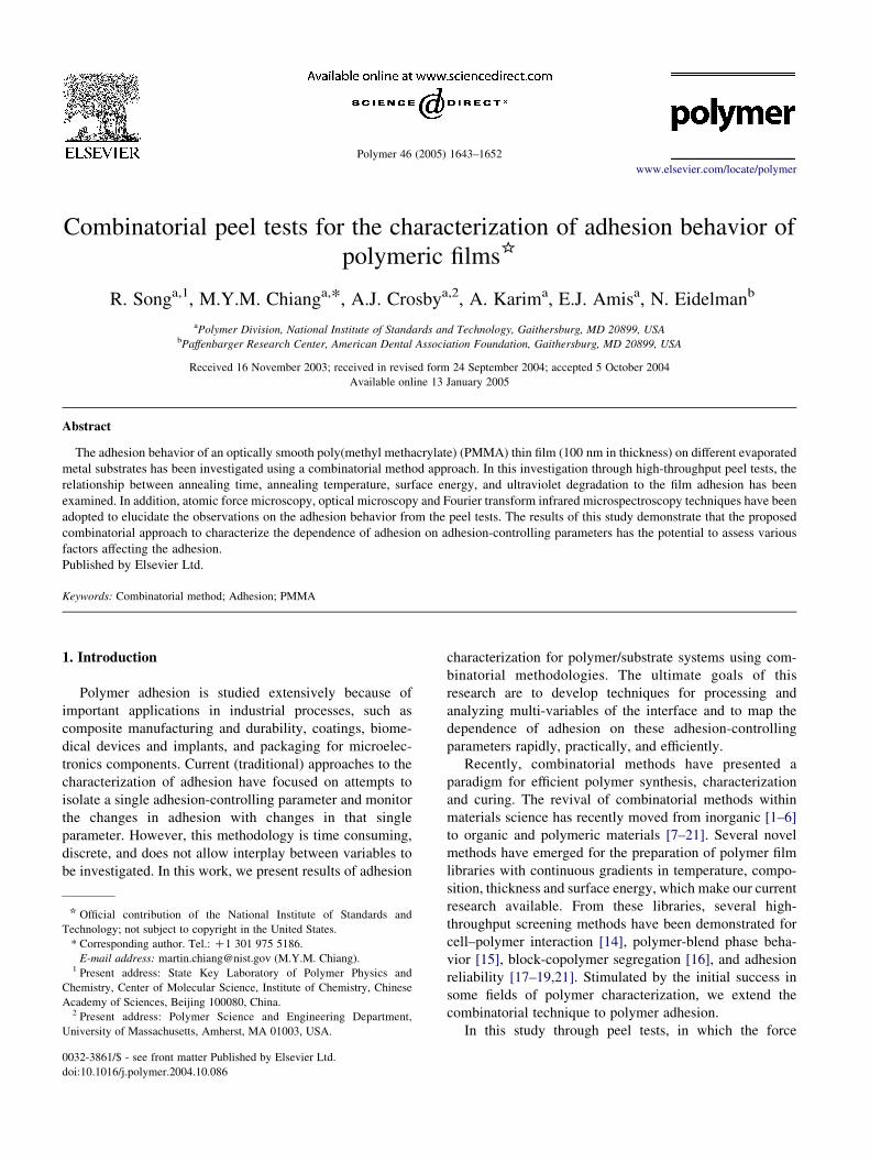
Fig. 2. Schematic of peel test for peeling a commercial tape (as a backing
tape) adhered to a test film at 1808 peel angle. l is the original sample
(bonded) length. lp is the peeled length. lo is the bonded length after peeling.
2.3. Temperature gradient stage and peel tests
An aluminum plate, (102!62!4) mm3, having a
temperature gradient was used as a temperature stage for
studying the annealing temperature effect on the develop-
ment of adhesion between a film and a substrate. One edge
of the plate has a higher temperature from a metal heating
bar controlled by a thermal controller, and the opposite edge
has a lower temperature from a refrigerating bath circulator
(RTE-220, Neslab, Newington, NH) filled with constant
temperature fluid. This setup can offer a controllable
temperature range from 30 to 240 8C with fluctuations less
than G2 8C. The film/substrate sample is placed on a
location in the temperature stage based on a desired
temperature gradient.
The adhesion of a film/substrate interface was evaluated
in terms of the peel energy (GIC) using a peel test [23] on the
TX.XT2I texture analyzer (Stable Micro System, Surrey,
UK). The test was carried out at ambient temperature by
peeling a commercial tape (3M) adhered to the PMMA of
the film/substrate sample at 1808 peel angle and a 1.0 mm/s
peel rate (Fig. 2). The backing tape was grabbed for peeling,
since the test film was very thin (ca. 100 nm in thickness)
such that a direct peeling of the film from the substrate is
impossible. The adhesion between the tape and the film is
assumed to be stronger than that between the film and the
substrate. Results from separate experiments (not reported
here) indicate that the assumption is valid. To obtain an
intimate contact between the tape and the film, the air
bubbles between the tape and the film/substrate sample were
squeezed out with a blunt knife-edge and cotton swabs. If
the extension of the peel strip (PMMA film and the tape) is
negligible, the GIC can be determined through the following
equation:
GIC ZPð1Kcos qÞ=bZ 2P=b ðfor qZ 1808Þ (1)
where P is the peel force, and b is the width of the test
sample. In our study, the GIC was obtained from the average
of at least 3 peel tests per film/substrate system.
2.4. UV degradation, AFM, and FTIR
For the UV degradation experiment, a UVO (UV Ozone)
cleaner (Model 342 UV Cleaner, described in the above
section) was used. A PMMA thin film deposited on the Si
substrate (2.5 cm!7.5 cm) was placed in the UV cleaner
for treatment. The PMMA/Si sample was ink-marked in
different locations to form 7 regions. These regions were
under the same intensity of UV irradiation for varying
exposure times (2, 4, 8, 16, 32, 64 min; one region was
reserved for no irradiation). Right after each exposure time,
an exposed region was covered with a metal plate. By
repeating such a procedure, each region had a different UV
exposure time. Consequently, a UV degradation gradient
due to different exposure times would be produced on the
sample. The surface of the degraded sample was sub-
sequently characterized using AFM, optical microscopy,
and FTIR microspectroscopy techniques.
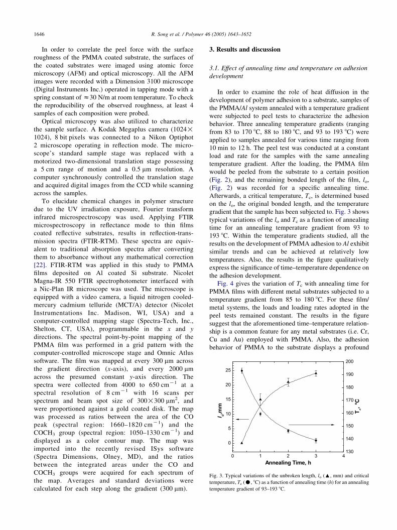
Fig. 3. Typical variations of the unbroken length, lo (:, mm) and critical
temperature, Tc (C, 8C) as a function of annealing time (h) for an annealing
temperature gradient of 93–193 8C.
R. Song et al. / Polymer 46 (2005) 1643–16521646
In order to correlate the peel force with the surface
roughness of the PMMA coated substrate, the surfaces of
the coated substrates were imaged using atomic force
microscopy (AFM) and optical microscopy. All the AFM
images were recorded with a Dimension 3100 microscope
(Digital Instruments Inc.) operated in tapping mode with a
spring constant ofz30 N/m at room temperature. To check
the reproducibility of the observed roughness, at least 4
samples of each composition were probed.
Optical microscopy was also utilized to characterize
the sample surface. A Kodak Megaplus camera (1024!1024), 8 bit pixels was connected to a Nikon Optiphot
2 microscope operating in reflection mode. The micro-
scope’s standard sample stage was replaced with a
motorized two-dimensional translation stage possessing
a 5 cm range of motion and a 0.5 mm resolution. A
computer synchronously controlled the translation stage
and acquired digital images from the CCD while scanning
across the samples.
To elucidate chemical changes in polymer structure
due to the UV irradiation exposure, Fourier transform
infrared microspectroscopy was used. Applying FTIR
microspectroscopy in reflectance mode to thin films
coated reflective substrates, results in reflection-trans-
mission spectra (FTIR-RTM). These spectra are equiv-
alent to traditional absorption spectra after converting
them to absorbance without any mathematical correction
[22]. FTIR-RTM was applied in this study to PMMA
films deposited on Al coated Si substrate. Nicolet
Magna-IR 550 FTIR spectrophotometer interfaced with
a Nic-Plan IR microscope was used. The microscope is
equipped with a video camera, a liquid nitrogen cooled-
mercury cadmium telluride (MCT/A) detector (Nicolet
Instrumentations Inc. Madison, WI, USA) and a
computer-controlled mapping stage (Spectra-Tech, Inc.,
Shelton, CT, USA), programmable in the x and y
directions. The spectral point-by-point mapping of the
PMMA film was performed in a grid pattern with the
computer-controlled microscope stage and Omnic Atlus
software. The film was mapped at every 300 mm across
the gradient direction (x-axis), and every 2000 mmacross the presumed constant y-axis direction. The
spectra were collected from 4000 to 650 cmK1 at a
spectral resolution of 8 cmK1 with 16 scans per
spectrum and beam spot size of 300!300 mm2, and
were proportioned against a gold coated disk. The map
was processed as ratios between the area of the CO
peak (spectral region: 1660–1820 cmK1) and the
COCH3 group (spectral region: 1050–1330 cmK1) and
displayed as a color contour map. The map was
imported into the recently revised ISys software
(Spectra Dimensions, Olney, MD), and the ratios
between the integrated areas under the CO and
COCH3 groups were acquired for each spectrum of
the map. Averages and standard deviations were
calculated for each step along the gradient (300 mm).
3. Results and discussion
3.1. Effect of annealing time and temperature on adhesion
development
In order to examine the role of heat diffusion in the
development of polymer adhesion to a substrate, samples of
the PMMA/Al system annealed with a temperature gradient
were subjected to peel tests to characterize the adhesion
behavior. Three annealing temperature gradients (ranging
from 83 to 170 8C, 88 to 180 8C, and 93 to 193 8C) were
applied to samples annealed for various time ranging from
10 min to 12 h. The peel test was conducted at a constant
load and rate for the samples with the same annealing
temperature gradient. After the loading, the PMMA film
would be peeled from the substrate to a certain position
(Fig. 2), and the remaining bonded length of the film, lo,
(Fig. 2) was recorded for a specific annealing time.
Afterwards, a critical temperature, Tc, is determined based
on the lo, the original bonded length, and the temperature
gradient that the sample has been subjected to. Fig. 3 shows
typical variations of the lo and Tc as a function of annealing
time for an annealing temperature gradient from 93 to
193 8C. Within the temperature gradients studied, all the
results on the development of PMMA adhesion to Al exhibit
similar trends and can be achieved at relatively low
temperatures. Also, the results in the figure qualitatively
express the significance of time–temperature dependence on
the adhesion development.
Fig. 4 gives the variation of Tc with annealing time for
PMMA films with different metal substrates subjected to a
temperature gradient from 85 to 180 8C. For these film/
metal systems, the loads and loading rates adopted in the
peel tests remained constant. The results in the figure
suggest that the aforementioned time–temperature relation-
ship is a common feature for any metal substrates (i.e. Cr,
Cu and Au) employed with PMMA. Also, the adhesion
behavior of PMMA to the substrate displays a profound
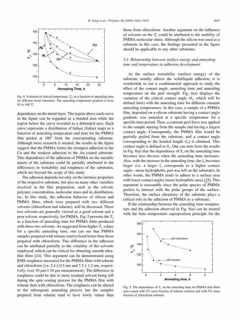
Fig. 4. Variation of critical temperature, Tc, as a function of annealing time
for different metal substrates. The annealing temperature gradient is from
85 to 180 8C.
Fig. 5. The dependence of Tc on the annealing time for PMMA thin films
spin-coated with 5% mass fraction of toluene solution and with 5% mass
fraction of chloroform solution.
R. Song et al. / Polymer 46 (2005) 1643–1652 1647
dependence on the metal layer. The region above each curve
in the figure can be regarded as a bonded area while the
region below the curve revealed as a debonded area. Each
curve represents a distribution of failure (failure map) as a
function of annealing temperature and time for the PMMA
film peeled at 1808 from the corresponding substrate.
Although more research is needed, the results in the figure
suggest that the PMMA forms the strongest adhesion to the
Cu and the weakest adhesion to the Au coated substrate.
This dependence of the adhesion of PMMA on the metallic
nature of the substrate could be partially attributed to the
differences in wettability and roughness of the substrates,
which are beyond the scope of this study.
The adhesion depends not only on the intrinsic properties
of the respective substrate, but also on many other variables
involved in the film preparation, such as the solvent,
polymer concentration, molecular mass and its distribution,
etc. In this study, the adhesion behavior of silicon and
PMMA films, which were prepared with two different
solvents (chloroform and toluene), will be discussed. These
two solvents are generally viewed as a good solvent and a
poor solvent, respectively, for PMMA. Fig. 5 presents the Tcas a function of annealing time for PMMA films produced
with these two solvents. As suggested from higher Tc values
for a specific annealing time, one can see that PMMA
samples prepared with toluene tend to bond better than those
prepared with chloroform. This difference in the adhesion
can be attributed partially to the volatility of the solvents
employed, which can be critical for obtaining smooth ultra-
thin films [24]. This argument can be demonstrated using
RMS roughness measured for the PMMA films with toluene
and chloroform (i.e. 2.4G0.5 nm and 7.5G1.2 nm, respect-
ively, over 10 mm!10 mm measurement). The difference in
roughness could be due to more residual solvent being left
during the spin coating process for the PMMA film with
toluene than with chloroform. The roughness can be altered
in the subsequent annealing process but the samples
prepared from toluene tend to have lower values than
those from chloroform. Another argument on the influence
of solvents on the Tc could be attributed to the mobility of
PMMA molecular chain. Although the silicon was used as a
substrate in this case, the findings presented in the figure
should be applicable to any other substrates.
3.2. Relationship between surface energy and annealing
time and temperature in adhesion development
As the surface wettability (surface energy) of the
substrate usually affects the solid/liquid adhesion, it is
worthwhile to use a combinatorial approach to study the
effect of the contact angle, annealing time and annealing
temperature on the peel strength. Fig. 6(a) displays the
variation of the critical contact angle (qc, which will be
defined later) with the annealing time for different constant
annealing temperatures. In this case, a sample of a PMMA
film, deposited on a silicon substrate having a contact angle
gradient, was annealed at a specific temperature for a
specific time period. Then, a constant peel force was applied
to the sample starting from the sample end having a largest
contact angle. Consequently, the PMMA film would be
partially peeled from the substrate, and a contact angle
corresponding to the bonded length (lo) is obtained. This
contact angle is defined as qc. One can note from the results
in Fig. 6(a) that the dependence of qc on the annealing time
becomes less obvious when the annealing time increases.
Also, with the increase in the annealing time, the lo becomes
larger (i.e. a larger lo corresponds to a higher contact
angle—more hydrophobic part was left on the substrate). In
other words, the PMMA tends to adhere to a surface area
with lower contact angles (more hydrophilic area) [25]. This
argument is reasonable since the polar species of PMMA
prefers to interact with the polar groups of the surface.
Therefore, the surface chemistry of the substrate plays a
critical role in the adhesion of PMMA to a substrate.
If the relationship between the annealing time–tempera-
ture and the adhesion observed in Fig. 6(a) can be treated
with the time–temperature superposition principle for the
Fig. 6. The critical contact angle gradient, qc, as a function of annealing
time for various annealing temperatures (a), the master curve of peel force
as function of annealing time and temperature for PMMA films peeled at
1808 from silicon substrates (b).
Fig. 7. The force–displacement curve from peel tests of PMMA/silicon
samples with different peel rates: 0.2 mm/s (a), 2 mm/s (b).
R. Song et al. / Polymer 46 (2005) 1643–16521648
modulus of a viscoelastic material, one may apply this
equivalence principle to the annealing time–temperature,
such that a correspondent time (tc) for a certain annealing
time (ta) is:
tc Z aT ta (2)
where aT is the shift factor, and aT can be related to
temperature (T) through the WLF equation [26]:
log aT ZKC1ðT KTgÞ
C2 CT KTg(3)
where C1 and C2 are constants and vary rather slightly from
polymer to polymer. If taking C1Z17.4 and C2Z51.6
(universal constants) and applying the data in Fig. 6(a) to
Eqs. (2) and (3), one can construct a master curve that
illustrates the dependence of the critical contact angle (for
the film peeled at 1808 from the substrate) on the arbitrary
choice of annealing time and temperature (Fig. 6(b)).
Assuming that the WLF equation is applicable [27], the
results in the figure also provide a failure distribution
(failure map) as a function of contact angle and annealing
temperature and time. This failure map provides designing
engineers and manufacturers a tool to determine materials
(or the critical surface energy) needed for practical
considerations of the adhesive bond of interest.
Fig. 7(a) presents the peel force (P)—displacement curve
for a peel test of a PMMA/silicon sample, where the silicon
substrate has a contact angle gradient ranging from about 30
to 808. The peel force reaches its maximum in value at a
contact angle near 508 and is not directly proportional to the
contact angle. This observation on the relationship between
peel force and the contact angle can be repeated for different
rates (e.g. Fig. 7(b).)
In separate peel tests, commercial tapes (identical to the
backing tape used in the previous tests) were directly peeled
from different materials with a variety of surface energies at
a peel angle of 1808. A plot of the peel force relative to the
surface energy of the samples is shown in Fig. 8. These
different materials include silicon, glass, aluminum,
PMMA, and PTFE (labeled in the figure). The surface
energies of those materials listed in the figure were
calculated from the measurements of contact angles of a
polar fluid (pure H2O) and a non-polar fluid (diiodomethane,
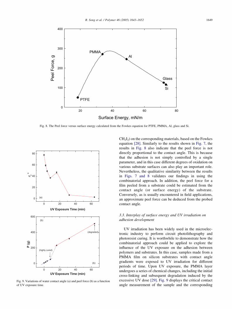
Fig. 8. The Peel force versus surface energy calculated from the Fowkes equation for PTFE, PMMA, Al, glass and Si.
Fig. 9. Variations of water contact angle (a) and peel force (b) as a function
of UV exposure time.
R. Song et al. / Polymer 46 (2005) 1643–1652 1649
CH2I2) on the corresponding materials, based on the Fowkes
equation [28]. Similarly to the results shown in Fig. 7, the
results in Fig. 8 also indicate that the peel force is not
directly proportional to the contact angle. This is because
that the adhesion is not simply controlled by a single
parameter, and in this case different degrees of oxidation on
various substrate surfaces can also play an important role.
Nevertheless, the qualitative similarity between the results
in Figs. 7 and 8 validates our findings in using the
combinatorial approach. In addition, the peel force for a
film peeled from a substrate could be estimated from the
contact angle (or surface energy) of the substrate.
Conversely, as is usually encountered in field applications,
an approximate peel force can be deduced from the probed
contact angle.
3.3. Interplay of surface energy and UV irradiation on
adhesion development
UV irradiation has been widely used in the microelec-
tronic industry to perform circuit photolithography and
photoresist curing. It is worthwhile to demonstrate how the
combinatorial approach could be applied to explore the
influence of the UV exposure on the adhesion between
polymers and substrates. In this case, samples made from a
PMMA film on silicon substrates with contact angle
gradients were exposed to UV irradiation for different
periods of time. Upon UV exposure, the PMMA layer
undergoes a series of chemical changes, including the initial
cross-linking and subsequent degradation induced by the
excessive UV dose [29]. Fig. 9 displays the critical contact
angle measurement of the sample and the corresponding
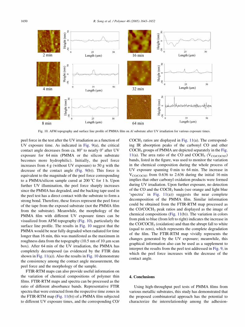
Fig. 10. AFM topography and surface line profile of PMMA film on Al substrate after UV irradiation for various exposure times.
R. Song et al. / Polymer 46 (2005) 1643–16521650
peel force in the test after the UV irradiation as a function of
UV exposure time. As indicated in Fig. 9(a), the critical
contact angle decreases from ca. 808 to nearly 08 after UV
exposure for 64 min (PMMA or the silicon substrate
becomes more hydrophilic). Initially, the peel force
increases from 4 g (without UV exposure) to 50 g with the
decrease of the contact angle (Fig. 9(b)). This force is
equivalent to the magnitude of the peel force corresponding
to a PMMA/silicon sample cured at 200 8C for 1 h. Upon
further UV illumination, the peel force sharply increases
since the PMMA has degraded, and the backing tape used in
the peel test has a direct contact with the substrate to form a
strong bond. Therefore, these forces represent the peel force
of the tape from the exposed substrate (not the PMMA film
from the substrate). Meanwhile, the morphology of the
PMMA film with different UV exposure times can be
visualized from AFM topography (Fig. 10), particularly the
surface line profile. The results in Fig. 10 suggest that the
PMMAwould be near fully degraded when radiated for time
longer than 16 min, this was manifested as the maximum in
roughness data from the topography (10.5 nm of 10 mm scan
box). After 64 min of the UV irradiation, the PMMA has
completely decomposed (as evidenced by the FTIR data
shown in Fig. 11(a)). Also the results in Fig. 10 demonstrate
the consistency among the contact angle measurement, the
peel force and the morphology of the sample.
FTIR-RTM maps can also provide useful information on
the variation of chemical compositions of polymer thin
films. FTIR-RTM maps and spectra can be processed as the
ratio of different absorbance bands. Representative FTIR
spectra that were extracted from the respective time zones in
the FTIR-RTM map (Fig. 11(b)) of a PMMA film subjected
to different UV exposure times, and the corresponding CO/
COCH3 ratios are displayed in Fig. 11(a). The correspond-
ing IR absorption peaks of the carbonyl CO and ether
COCH3 groups of PMMA are depicted separately in the Fig.
11(a). The area ratio of the CO and COCH3 (VCO/COCH3)
bands, listed in the figure, was used to monitor the variation
in the chemical composition during the whole process of
UV exposure spanning 0 min to 64 min. The increase in
VCO/COCH3 from 0.636 to 2.636 during the initial 16 min
implies that other carbonyl oxidation products were formed
during UV irradiation. Upon further exposure, no detection
of the CO and the COCH3 bands (see orange and light blue
‘spectra’ in Fig. 11(a)) suggests the near complete
decomposition of the PMMA film. Similar information
could be obtained from the FTIR-RTM map processed as
the CO/COCH3 peak ratios and displayed as the image of
chemical compositions (Fig. 11(b)). The variation in colors
from pink to blue (from left to right) indicates the increase in
the CO/COCH3 (oxidation) and than the abrupt fall to white
(equal to zero), which represents the complete degradation
of the film. The FTIR-RTM map vividly represents the
changes generated by the UV exposure; meanwhile, this
graphical information also can be used as a supplement to
interpret the results from the peel test addressed in Fig. 9, in
which the peel force increases with the decrease of the
contact angle.
4. Conclusions
Using high-throughput peel tests of PMMA films from
various metallic substrates, this study has demonstrated that
the proposed combinatorial approach has the potential to
characterize the interrelationship among the adhesion-
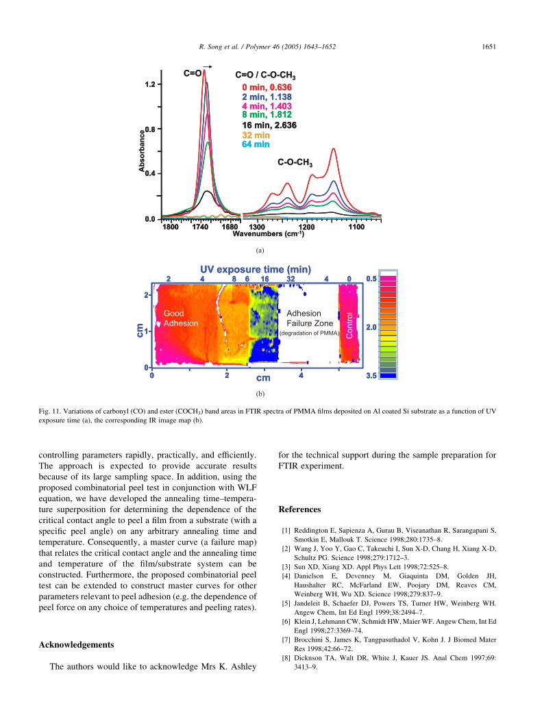
Fig. 11. Variations of carbonyl (CO) and ester (COCH3) band areas in FTIR spectra of PMMA films deposited on Al coated Si substrate as a function of UV
exposure time (a), the corresponding IR image map (b).
R. Song et al. / Polymer 46 (2005) 1643–1652 1651
controlling parameters rapidly, practically, and efficiently.
The approach is expected to provide accurate results
because of its large sampling space. In addition, using the
proposed combinatorial peel test in conjunction with WLF
equation, we have developed the annealing time–tempera-
ture superposition for determining the dependence of the
critical contact angle to peel a film from a substrate (with a
specific peel angle) on any arbitrary annealing time and
temperature. Consequently, a master curve (a failure map)
that relates the critical contact angle and the annealing time
and temperature of the film/substrate system can be
constructed. Furthermore, the proposed combinatorial peel
test can be extended to construct master curves for other
parameters relevant to peel adhesion (e.g. the dependence of
peel force on any choice of temperatures and peeling rates).
Acknowledgements
The authors would like to acknowledge Mrs K. Ashley
for the technical support during the sample preparation for
FTIR experiment.
References
[1] Reddington E, Sapienza A, Gurau B, Viseanathan R, Sarangapani S,
Smotkin E, Mallouk T. Science 1998;280:1735–8.
[2] Wang J, Yoo Y, Gao C, Takeuchi I, Sun X-D, Chang H, Xiang X-D,
Schultz PG. Science 1998;279:1712–3.
[3] Sun XD, Xiang XD. Appl Phys Lett 1998;72:525–8.
[4] Danielson E, Devenney M, Giaquinta DM, Golden JH,
Haushalter RC, McFarland EW, Poojary DM, Reaves CM,
Weinberg WH, Wu XD. Science 1998;279:837–9.
[5] Jandeleit B, Schaefer DJ, Powers TS, Turner HW, Weinberg WH.
Angew Chem, Int Ed Engl 1999;38:2494–7.
[6] Klein J, Lehmann CW, Schmidt HW,MaierWF. Angew Chem, Int Ed
Engl 1998;27:3369–74.
[7] Brocchini S, James K, Tangpasuthadol V, Kohn J. J Biomed Mater
Res 1998;42:66–72.
[8] Dicknson TA, Walt DR, White J, Kauer JS. Anal Chem 1997;69:
3413–9.
R. Song et al. / Polymer 46 (2005) 1643–16521652
[9] Newkome GR, Weis CD, Moorefiedl CN, Baker GR, Childs BJ,
Epperson J. Angew Chem, Int Ed Engl 1998;37:307–11.
[10] Gravert DJ, Datta A, Wentworth P, Janda KD. J Am Chem Soc 1998;
120:9481–5.
[11] Reynolds CH. J Combinat Chem 1999;1:297–304.
[12] Takeuchi T, Fukuma D, Matsui J. Anal Chem 1999;71:285–93.
[13] Schmitz C, Posch P, Thelakkat M, Schmidt HW. Macromol Symp
2000;154:209–21.
[14] Gross M, Muller DC, Nothofer HG, Sherf U, Neher D, Brauchle C,
Meerholz K. Nature 2000;405:661–4.
[15] Meredith JC, Karim A, Amis EJ. Macromolecules 2000;33:5760–6.
[16] Smith AP, Douglas J, Meredith JC, Karim A, Amis EJ. Phys Rev Lett
2001;87:15503–6.
[17] Chiang MYM, Wu W, He JM, Amis EJ. Thin Solid Films 2003;437:
197–203.
[18] Chiang MYM, Song R, He JM, Karim A, Amis EJ. In: Kinloch AJ,
editor. Fracture of polymers, composites and adhesives. Oxford:
Elsevier; 2003.
[19] Crosby AJ. J Mater Sci 2003;38:1–11.
[20] Amis EJ. Nat Mater 2004;3:83–5.
[21] Chiang MYM, Song R, Crosby AJ, Karim A, Chiang CK, Amis EJ.
Thin Solid Film 2004 [in press].
[22] Eidelman N, Simon CG. J Res Natl Inst Stand Technol 2004;109(2):
219–31.
[23] Lee I, Wool RP. Macromolecules 2000;33:2680–7.
[24] Strawhecker KE, Kumar SK. Macromolecules 2001;34:4669–72.
[25] Pfau A, Sander R, Kirsch S. Langmuir 2002;18:2880–8.
[26] Williams ML, Landel RF, Ferry JD. J Am Chem Soc 1955;77:3701.
[27] Chiang MYM, McKenna GB, Yuan J. Polym Eng Sci 1994;34:
1815–22.
[28] Fowkes FM. Ind Eng Chem 1964;56:40–8.
[29] Horiuchi S, Fujita T, Hayakawa T, Nakao Y. Adv Mater 2003;15:
1449–52.
Related Documents