Combinational Circuits

Combinational Circuits. Analysis Diagram Designing Combinational Circuits In general we have to do following steps: 1. Problem description 2. Input/output.
Dec 14, 2015
Welcome message from author
This document is posted to help you gain knowledge. Please leave a comment to let me know what you think about it! Share it to your friends and learn new things together.
Transcript

Combinational Circuits
Analysis Diagram
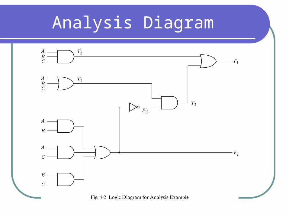
Designing Combinational Circuits
In general we have to do following steps:
1. Problem description
2. Input/output of the circuit
3. Define truth table
4. Simplification for each output
5. Draw the circuit

Half Adders
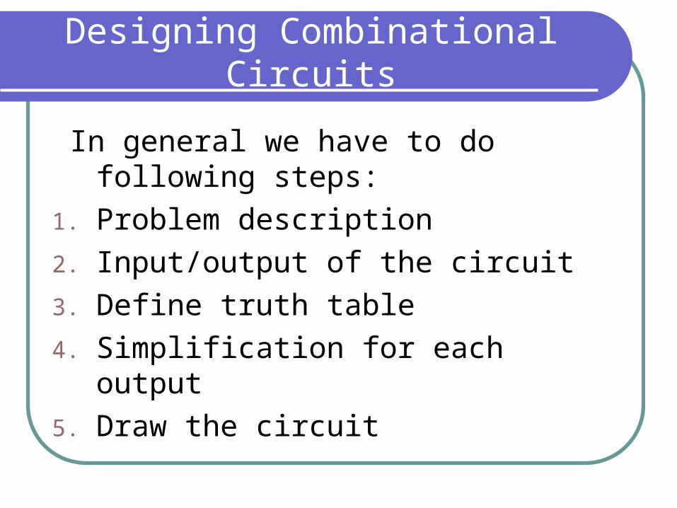
Maps for Full ADDER

SOP for ADDERS

Full ADDER using Half ADDER
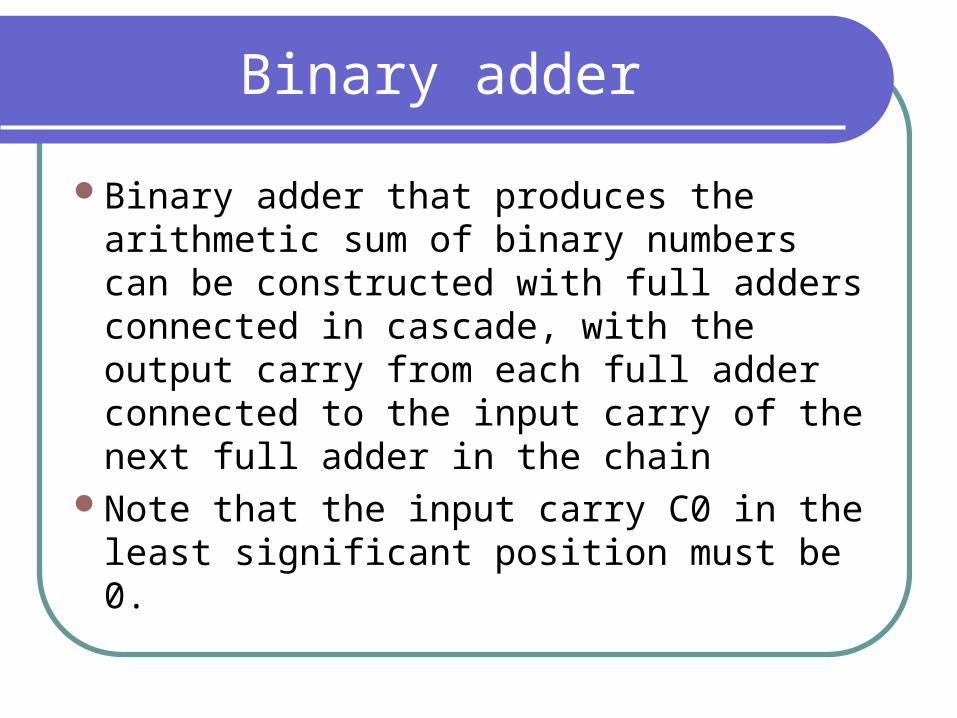
Binary adder
Binary adder that produces the arithmetic sum of binary numbers can be constructed with full adders connected in cascade, with the output carry from each full adder connected to the input carry of the next full adder in the chain
Note that the input carry C0 in the least significant position must be 0.
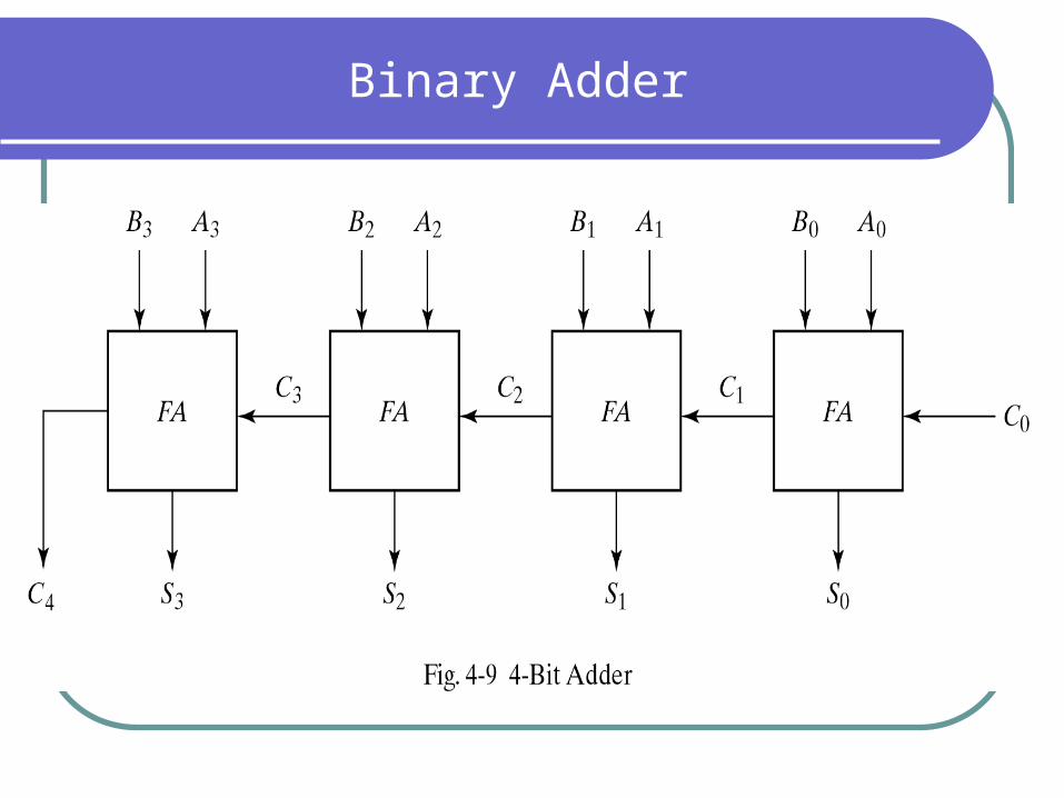
Binary Adder
Binary Adder
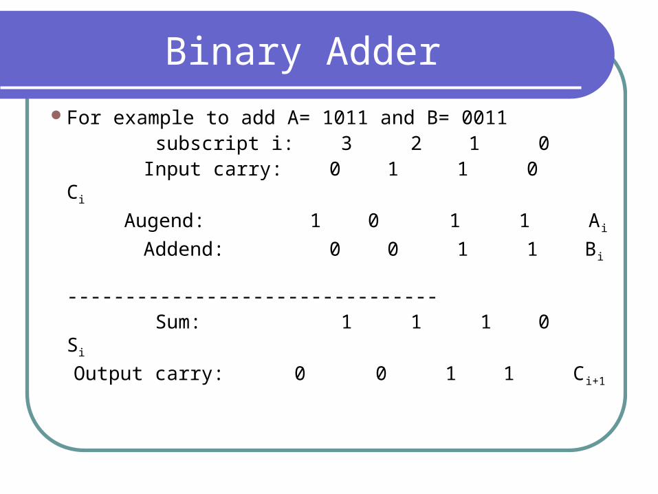
For example to add A= 1011 and B= 0011 subscript i: 3 2 1 0
Input carry: 0 1 1 0 Ci
Augend: 1 0 1 1 Ai
Addend: 0 0 1 1 Bi --------------------------------
Sum: 1 1 1 0 Si
Output carry: 0 0 1 1 Ci+1

Binary Subtractor
The subtraction A – B can be done by taking the 2’s complement of B and adding it to A because A- B = A + (-B)
It means if we use the inverters to make 1’s complement of B (connecting each Bi to an inverter) and then add 1 to the least significant bit (by setting carry C0 to 1) of binary adder, then we can make a binary subtractor.

4 bit 2’s complement Subtractor
= 1
Adder Subtractor
The addition and subtraction can be combined into one circuit with one common binary adder (see next slide).
The mode M controls the operation. When M=0 the circuit is an adder when M=1 the circuit is subtractor. It can be don by using exclusive-OR for each Bi and M. Note that 1 ⊕ x = x’ and 0 ⊕ x = x
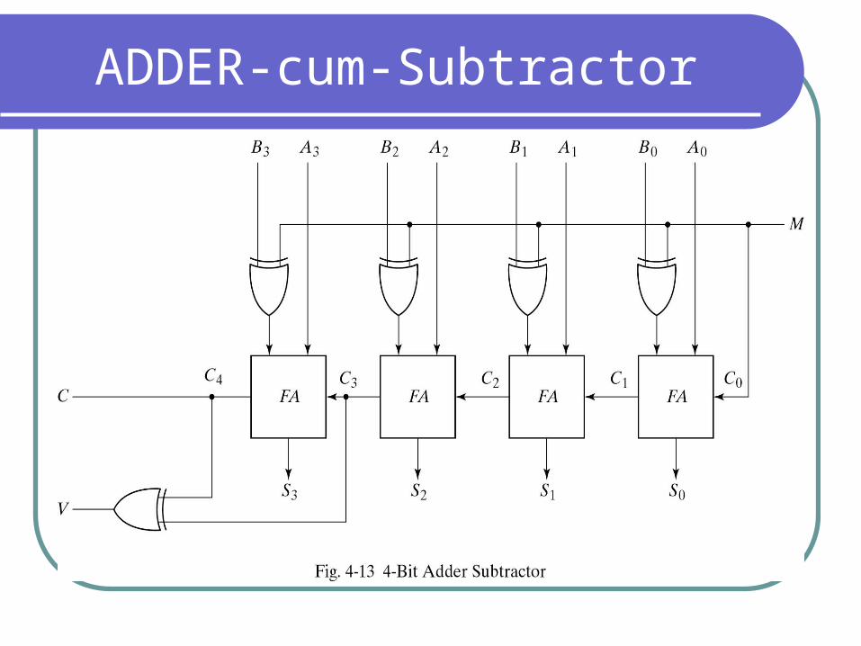
ADDER-cum-Subtractor

Checking Overflow
Note that in the previous slide if the numbers considered to be signed V detects overflow. V=0 means no overflow and V=1 means the result is wrong because of overflow
Overflow can be happened when adding two numbers of the same sign (both negative or positive) and result can not be shown with the available bits. It can be detected by observing the carry into sign bit and carry out of sign bit position. If these two carries are not equal an overflow occurred. That is why these two carries are applied to exclusive-OR gate to generate V.
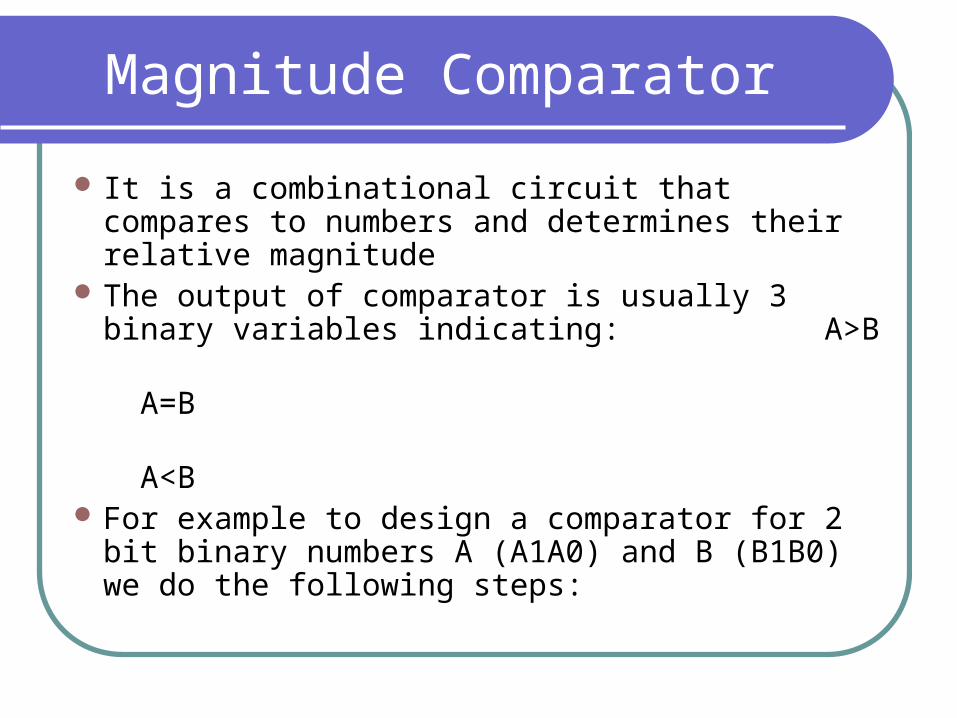
Magnitude Comparator
It is a combinational circuit that compares to numbers and determines their relative magnitude
The output of comparator is usually 3 binary variables indicating: A>B
A=B A<B For example to design a comparator for 2 bit
binary numbers A (A1A0) and B (B1B0) we do the following steps:
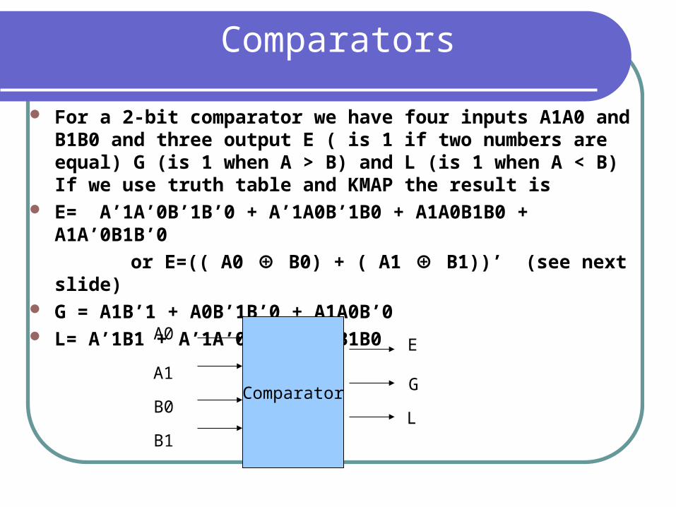
Comparators
For a 2-bit comparator we have four inputs A1A0 and B1B0 and three output E ( is 1 if two numbers are equal) G (is 1 when A > B) and L (is 1 when A < B) If we use truth table and KMAP the result is
E= A’1A’0B’1B’0 + A’1A0B’1B0 + A1A0B1B0 + A1A’0B1B’0
or E=(( A0 ⊕ B0) + ( A1 ⊕ B1))’ (see next slide) G = A1B’1 + A0B’1B’0 + A1A0B’0 L= A’1B1 + A’1A’0B0 + A’0B1B0
Comparator
A0
A1
B0
B1
E
G
L

Magnitude Comparator
Here we use simpler method to find E (called X) and G (called Y) and L (called Z)
A=B if all Ai= Bi Ai Bi Xi ------------ 0 0 1 0 1 0 1 0 0 1 1 0 It means X0 = A0B0 + A’0B’0 and X1= A1B1 + A’1B’1 If X0=1 and X1=1 then A0=B0 and A1=B1Thus, if A=B then X0X1 = 1 it means X= (A0B0 + A’0B’0)(A1B1 + A’1B’1) since (x ⊕ y)’ = (xy +x’y’) X= ( A0 ⊕ B0)’ ( A1 ⊕ B1)’ = (( A0 ⊕ B0) + ( A1 ⊕ B1))’ It means for X we can NOR the result of two exclusive-OR gates

Magnitude Comparator
A>B means A1 B1 Y1 ------------ 0 0 0 0 1 0 1 0 1 1 1 0 if A1=B1 (X1=1) then A0 should be 1 and B0 should be 0 A0 B0 Y0 ------------ 0 0 1 0 1 0 1 0 0 1 1 0 For A> B: A1 > B1 or A1 =B1 and A0 > B0It means Y= A1B’1 + X1A0B’0 should be 1 for A>B

Magnitude Comparator
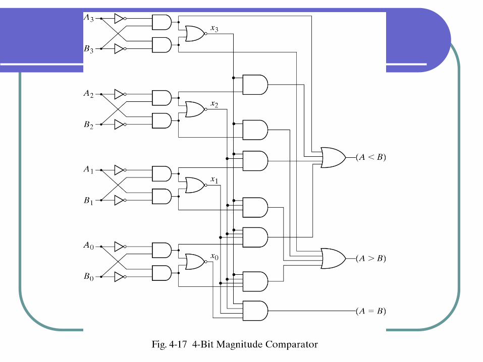
For B>A B1 > A1 or A1=B1 and B0> A0 z= A’1B1 + X1A’0B0 The procedure for binary numbers with more than 2
bits can also be found in the similar way. For example next slide shows the 4-bit magnitude comparator, in which
(A= B) = x3x2x1x0(A> B) = A3B’3 + x3A2B’2 + x3x2A1B’1+ x3x2x1A0B’0(A< B) = A’3B3 + x3A’2B2 + x3x2A’1B1+ x3x2x1A’0B0
Related Documents