1730 | Chem. Soc. Rev., 2017, 46, 1730--1759 This journal is © The Royal Society of Chemistry 2017 Cite this: Chem. Soc. Rev., 2017, 46, 1730 Colloidal metal oxide nanocrystals as charge transporting layers for solution-processed light-emitting diodes and solar cells Xiaoyong Liang,† a Sai Bai,† b Xin Wang, a Xingliang Dai, a Feng Gao, b Baoquan Sun, c Zhijun Ning, d Zhizhen Ye* a and Yizheng Jin* e Colloidal metal oxide nanocrystals offer a unique combination of excellent low-temperature solution processability, rich and tuneable optoelectronic properties and intrinsic stability, which makes them an ideal class of materials as charge transporting layers in solution-processed light-emitting diodes and solar cells. Developing new material chemistry and custom-tailoring processing and properties of charge transporting layers based on oxide nanocrystals hold the key to boosting the efficiency and lifetime of all-solution-processed light-emitting diodes and solar cells, and thereby realizing an unprecedented generation of high-performance, low-cost, large-area and flexible optoelectronic devices. This review aims to bridge two research fields, chemistry of colloidal oxide nanocrystals and interfacial engineering of optoelectronic devices, focusing on the relationship between chemistry of colloidal oxide nano- crystals, processing and properties of charge transporting layers and device performance. Synthetic chemistry of colloidal oxide nanocrystals, ligand chemistry that may be applied to colloidal oxide nanocrystals and chemistry associated with post-deposition treatments are discussed to highlight the ability of optimizing processing and optoelectronic properties of charge transporting layers. Selected examples of solution-processed solar cells and light-emitting diodes with oxide-nanocrystal charge transporting layers are examined. The emphasis is placed on the correlation between the properties of oxide-nanocrystal charge transporting layers and device performance. Finally, three major challenges that need to be addressed in the future are outlined. We anticipate that this review will spur new material design and simulate new chemistry for colloidal oxide nanocrystals, leading to charge transporting layers and solution-processed optoelectronic devices beyond the state-of-the-art. 1. Introduction The exciting discoveries and tremendous progress of material chemistry create families of solution-processed semiconductors, including conjugated polymers, 1,2 colloidal quantum dots (QDs) 3–5 and organic–inorganic hybrid lead–halide hybrid perovskites. 6,7 These materials with intriguing optoelectronic properties can be processed as thin films by high-throughput and vacuum-free printing and coating techniques, such as inkjet-printing, roll-to- roll printing and blade-coating. 8–16 Many printing and coating procedures can be completed at low temperatures. Therefore, they are compatible with flexible and light-weight plastic sub- strates. These merits promise an unprecedented generation of low-cost, large-area and flexible light-emitting diodes (LEDs) and solar cells processed by solution-based techniques. High-performance LEDs and solar cells are no doubt the results of extraordinary cooperation of multiple functional components. For the state-of-the-art solution-processed LEDs or solar cells, charge transporting layers (CTLs), i.e. electron transporting layers (ETLs) and hole transporting layers (HTLs), are essential components (Fig. 1). CTLs affect not only charge injection (or extraction) into (or out of) the active layers, but also many other elementary physical processes for device operation, such as interfacial charge recombination and light extraction (or light absorption) in LEDs (or solar cells). The integration of a State Key Laboratory of Silicon Materials, School of Materials Science and Engineering, Zhejiang University, Hangzhou 310027, People’s Republic of China. E-mail: [email protected] b Department of Physics, Chemistry and Biology (IFM), Linko¨ping University, SE-581 83 Linko¨ping, Sweden c Jiangsu Key Laboratory for Carbon-Based Functional Materials & Devices, Institute of Functional Nano & Soft Materials (FUNSOM), Soochow University, Suzhou 215123, People’s Republic of China d Shanghai Tech University, China e Center for Chemistry of High-Performance & Novel Materials, State Key Laboratory of Silicon Materials, Department of Chemistry, Zhejiang University, Hangzhou 310027, People’s Republic of China. E-mail: [email protected] † These authors contributed equally to this work. Received 17th February 2016 DOI: 10.1039/c6cs00122j rsc.li/chem-soc-rev Chem Soc Rev REVIEW ARTICLE Open Access Article. Published on 28 February 2017. Downloaded on 1/23/2022 8:09:29 PM. This article is licensed under a Creative Commons Attribution 3.0 Unported Licence. View Article Online View Journal | View Issue

Welcome message from author
This document is posted to help you gain knowledge. Please leave a comment to let me know what you think about it! Share it to your friends and learn new things together.
Transcript
1730 | Chem. Soc. Rev., 2017, 46, 1730--1759 This journal is©The Royal Society of Chemistry 2017
Cite this: Chem. Soc. Rev., 2017,
46, 1730
Colloidal metal oxide nanocrystals as chargetransporting layers for solution-processedlight-emitting diodes and solar cells
Xiaoyong Liang,†a Sai Bai,†b Xin Wang,a Xingliang Dai,a Feng Gao,b Baoquan Sun,c
Zhijun Ning,d Zhizhen Ye*a and Yizheng Jin*e
Colloidal metal oxide nanocrystals offer a unique combination of excellent low-temperature solution
processability, rich and tuneable optoelectronic properties and intrinsic stability, which makes them an
ideal class of materials as charge transporting layers in solution-processed light-emitting diodes and
solar cells. Developing new material chemistry and custom-tailoring processing and properties of charge
transporting layers based on oxide nanocrystals hold the key to boosting the efficiency and lifetime of
all-solution-processed light-emitting diodes and solar cells, and thereby realizing an unprecedented
generation of high-performance, low-cost, large-area and flexible optoelectronic devices. This review
aims to bridge two research fields, chemistry of colloidal oxide nanocrystals and interfacial engineering
of optoelectronic devices, focusing on the relationship between chemistry of colloidal oxide nano-
crystals, processing and properties of charge transporting layers and device performance. Synthetic
chemistry of colloidal oxide nanocrystals, ligand chemistry that may be applied to colloidal oxide
nanocrystals and chemistry associated with post-deposition treatments are discussed to highlight the
ability of optimizing processing and optoelectronic properties of charge transporting layers. Selected
examples of solution-processed solar cells and light-emitting diodes with oxide-nanocrystal charge
transporting layers are examined. The emphasis is placed on the correlation between the properties of
oxide-nanocrystal charge transporting layers and device performance. Finally, three major challenges
that need to be addressed in the future are outlined. We anticipate that this review will spur new
material design and simulate new chemistry for colloidal oxide nanocrystals, leading to charge
transporting layers and solution-processed optoelectronic devices beyond the state-of-the-art.
1. Introduction
The exciting discoveries and tremendous progress of materialchemistry create families of solution-processed semiconductors,including conjugated polymers,1,2 colloidal quantum dots (QDs)3–5
and organic–inorganic hybrid lead–halide hybrid perovskites.6,7
These materials with intriguing optoelectronic properties can beprocessed as thin films by high-throughput and vacuum-freeprinting and coating techniques, such as inkjet-printing, roll-to-roll printing and blade-coating.8–16 Many printing and coatingprocedures can be completed at low temperatures. Therefore,they are compatible with flexible and light-weight plastic sub-strates. These merits promise an unprecedented generation oflow-cost, large-area and flexible light-emitting diodes (LEDs)and solar cells processed by solution-based techniques.
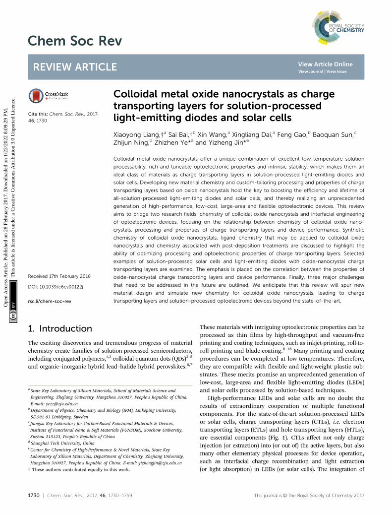
High-performance LEDs and solar cells are no doubt theresults of extraordinary cooperation of multiple functionalcomponents. For the state-of-the-art solution-processed LEDsor solar cells, charge transporting layers (CTLs), i.e. electrontransporting layers (ETLs) and hole transporting layers (HTLs),are essential components (Fig. 1). CTLs affect not only chargeinjection (or extraction) into (or out of) the active layers, but alsomany other elementary physical processes for device operation,such as interfacial charge recombination and light extraction(or light absorption) in LEDs (or solar cells). The integration of
a State Key Laboratory of Silicon Materials, School of Materials Science and
Engineering, Zhejiang University, Hangzhou 310027, People’s Republic of China.
E-mail: [email protected] Department of Physics, Chemistry and Biology (IFM), Linkoping University,
SE-581 83 Linkoping, Swedenc Jiangsu Key Laboratory for Carbon-Based Functional Materials & Devices,
Institute of Functional Nano & Soft Materials (FUNSOM), Soochow University,
Suzhou 215123, People’s Republic of Chinad Shanghai Tech University, Chinae Center for Chemistry of High-Performance & Novel Materials, State Key
Laboratory of Silicon Materials, Department of Chemistry, Zhejiang University,
Hangzhou 310027, People’s Republic of China. E-mail: [email protected]
† These authors contributed equally to this work.
Received 17th February 2016
DOI: 10.1039/c6cs00122j
rsc.li/chem-soc-rev
Chem Soc Rev
REVIEW ARTICLE
Ope
n A
cces
s A
rtic
le. P
ublis
hed
on 2
8 Fe
brua
ry 2
017.
Dow
nloa
ded
on 1
/23/
2022
8:0
9:29
PM
. T
his
artic
le is
lice
nsed
und
er a
Cre
ativ
e C
omm
ons
Attr
ibut
ion
3.0
Unp
orte
d L
icen
ce.
View Article OnlineView Journal | View Issue
This journal is©The Royal Society of Chemistry 2017 Chem. Soc. Rev., 2017, 46, 1730--1759 | 1731
CTLs with desirable properties is critical in terms of improvingdevice performance.
For large-scale production of solution-processed optoelec-tronics, ideally, not only the active layers but also all the othercomponents should be able to be deposited by solution-basedtechniques. In this regard, various solution-processed materials
have been explored as CTLs. Among them, colloidal metal oxidenanocrystals have attracted great interest.17–24 The best example isETLs based on colloidal ZnO nanocrystals, which have beenemployed in several best-performing proto-type devices, includingthe quantum-dot LEDs (QLEDs) developed by our group,18 thequantum-dot solar cells (QDSCs) developed by the Sargentgroup22 and the perovskite LEDs developed by the Wang andHuang group.23 Many other reports showed that colloidal oxidenanocrystals with high work function, e.g. NiO nanocrystals,24,25
can be used to fabricate high-quality HTLs for LEDs and solarcells. Furthermore, colloidal oxide nanocrystals are fully compa-tible with large-scale industrial production. For example, Krebsand co-workers prepared polymer solar cell modules in whichZnO nanocrystals were deposited as ETLs by a modified slot-diecoating procedure.26,27 These facts highlight a promising futureof integrating colloidal oxide nanocrystals as CTLs in solution-processed LEDs and solar cells to achieve high-performance,low-cost and large-area devices.
This review article aims to provide illustrative accounts onthe current status of CTLs based on oxide nanocrystals. Theprogress of utilizing colloidal oxide nanocrystals as CTLs forsolution-processed LEDs and solar cells is based on the develop-ments of two important research fields, synthetic chemistryof colloidal oxide nanocrystals and interfacial engineering ofoptoelectronic devices. There are already good review articlesdedicated to either the synthetic chemistry of colloidal oxidenanocrystals28–32 or interfacial engineering of solution-processedoptoelectronics.33–43 Nevertheless, on the basis of our practices inthe past several years, we believe that there is a gap between thecommunity of chemists synthesizing oxide nanocrystals and thecommunity of researchers working on solution-processed opto-electronics. We would like to provide an in-depth review whichcorrelates chemistry of colloidal oxide nanocrystals, processingand optoelectronic properties of CTLs, and device performance ofsolution-processed solar cells and LEDs. A personal selection ofexamples is presented to systematize the knowledge bridging thetwo fields, chemistry of colloidal oxide nanocrystals and interfacialengineering of solution-processed LEDs and solar cells.
Fig. 1 Typical device structures of solution-processed (A) LEDs and(B) solar cells.
Sai Bai
Sai Bai obtained his PhD degree inMaterials Physics and Chemistryfrom Zhejiang University in 2014,focusing on solution processablemetal oxide films for optoelectronicapplications. He is current aVINNMER Fellow and Marie CurieFellow in Linkoping University,Sweden and University of Oxford,UK. His research interests includemetal oxide nanocrystals, organicphotovoltaics, perovskite solar cellsand perovskite light-emitting diodes. Yizheng Jin
Dr Yizheng Jin is a Professor ofChemistry at Zhejiang University,China. His research interestsencompass material chemistry,device engineering and devicephysics of solution-processedoptoelectronics. His research hasresulted in over 50 papers in peer-reviewed journals, including Nature,Nat. Photonics, J. Am. Chem. Soc.and Adv. Mater. Prof. Jin hasreceived several awards, includingNational Natural Science Funds forExcellent Young Scholar, Chinese
Chemical Society Award for Outstanding Young Chemist, Qiu-ShiYoung Scholars Award and Top 10 scientific advances of 2014 in China.
Xiaoyong Liang
Xiaoyong Liang is currently a PhDcandidate under the supervision ofProfessor Yizheng Jin in the StateKey Laboratory of Silicon Materials,School of Materials Science andEngineering at Zhejiang University.He has keen interest in interfacialengineering of solution-processedoptoelectronics using metal oxidesas charge-transport layers. Now heis working on quantum dot LEDs.
Review Article Chem Soc Rev
Ope
n A
cces
s A
rtic
le. P
ublis
hed
on 2
8 Fe
brua
ry 2
017.
Dow
nloa
ded
on 1
/23/
2022
8:0
9:29
PM
. T
his
artic
le is
lice
nsed
und
er a
Cre
ativ
e C
omm
ons
Attr
ibut
ion
3.0
Unp
orte
d L
icen
ce.
View Article Online
1732 | Chem. Soc. Rev., 2017, 46, 1730--1759 This journal is©The Royal Society of Chemistry 2017
We will begin with a summary of the general requirementsthat should be fulfilled by CTLs and point out the uniqueadvantages of colloidal oxide nanocrystals as CTLs. Next, a briefoverview of chemistry of colloidal oxide nanocrystals will bepresented. Synthetic chemistry of colloidal oxide nanocrystals,ligand chemistry that may be applicable to colloidal oxidenanocrystals and chemistry associated with post-depositiontreatments will be covered. The applications of colloidal oxidenanocrystals as CTLs in solar cells and LEDs will be summar-ized in the subsequent two chapters. Emphasis will be placedon the correlation between the properties of oxide-nanocrystalCTLs and device performance. The last chapter of this reviewwill list three major directions that we believe are critical forfuture development of oxide-nanocrystal CTLs.
2. General requirementsfor solution-processed CTLs
An essential requirement for solution-processed CTLs used inoptoelectronics is that they should be able to be integrated intodevices by solution-based methods. Formulation of inks withsufficiently high concentration and good stability is indispens-able to fabricate continuous and pinhole-free CTL films withcontrollable thickness. For all-solution processed devices,multiple layers, including the ETLs and HTLs, shall be processedfrom solutions. This often involves the use of orthogonal solventsystems for the deposition of different materials to avoid dis-solution of underlying layers. Moreover, processing of top CTLsshould exclude high-temperature annealing which may damagethe active layers or other components in the devices. Lowprocessing temperatures, i.e. o150 1C, are highly desirable sothat the processing procedures are compatible with flexiblesubstrates.
CTLs should be of good stability. First and foremost, CTLsthemselves must be sufficiently stable within the lifetime ofdevices. Second, all interfaces involving CTLs, e.g. the interfacesof active layer/ETL, active layer/HTL, cathode/ETL and anode/HTL, should be stable and the contact properties should notdeteriorate under long-time operational conditions. Third,in device operation, the active layers are in the excited states,which are generally sensitive to oxygen or moisture. Theenvironmental stability of devices can be greatly improved ifCTLs act as barriers for oxygen and moisture diffusion.
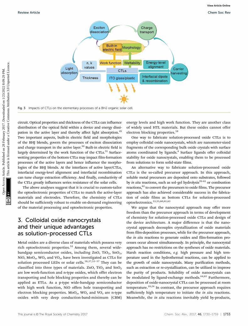
The chemistry of CTLs should be versatile and robust to allowsystematic and purposeful engineering of their optoelectronicproperties. Here we use QLEDs and bulk-heterojunction (BHJ)organic solar cells as examples to show that the optoelectronicproperties of CTLs, i.e. work function, band structure, conduc-tivity, intragap states, optical properties, etc., impact almost allthe elementary processes of device operation.
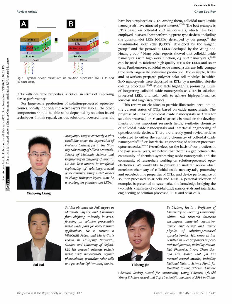
As shown in Fig. 2, elementary processes for QLED operationinvolve (1) charge injection from electrodes into CTLs,(2) charge transport in the CTLs, (3) charge injection from theCTLs into QD layers, (4) formation of excitons in the QDs,(5) radiative decay of the excitons to generate photons, and
(6) photon emission out of the devices. The energy-level alignmentat the interfaces of electrode/CTLs and QD/CTLs determines thecharge injection efficiency. Efficient charge injection into the QDsrelies on high conductivity of CTLs and negligible energy barriersat the interfaces to minimize potential-drops. Efficient excitonformation demands both balanced charge injection and effectivecharge confinement within the QD layer. Charge selective CTLswith good blocking properties are beneficial to realize effectivecharge confinement. Balanced charge injection requires modula-tion of both electron injection and hole injection so that injectionrates of the two types of carriers can match each other. In general,the ionization potential of many QD emitters is much higher thanthat of most organic semiconductors. Thus, conventional organicHTLs developed for organic emitters cannot achieve efficient holeinjection in QLEDs. Excess injection of one type of charge causesmany problems, such as a decrease of the fraction of injectedcharges that form excitons, charging of QDs which generates lessefficient trion emission,44,45 and deterioration of device lifetime.18
Interactions between CTLs and excitons formed in QDs oftencannot be neglected. This is because the QD films are typically2–4 monolayers in thickness. Charge recombination zones maylocate at regions close to CTLs. CTL-induced quenching can be animportant non-radiative decay channel.46–48 The intragap states ofCTLs may act as non-radiative interfacial recombination centers.46
The last elementary step, i.e. escape of the photons out of thedevices, largely depends on the optical properties and thickness ofthe CTLs. Extinction coefficients of the CTLs affect the energy lossof light. Refractive index and thickness of the CTLs are majorparameters that modify microcavity effects and energy loss causedby surface plasmon polaritons at the metal electrodes. Based onthe above analyses, we conclude that the optoelectronic propertiesof CTLs impact all the elementary physical processes in QLEDoperation.
Similarly, the optoelectronic properties of CTLs may influenceall the elementary processes of BHJ organic solar cells, in whichthe active layers consist of blends of electron donors and electronacceptors (Fig. 3). Elementary physical processes in BHJ organicsolar cells involve (1) light absorption to generate excitons,(2) exciton diffusion and dissociation at acceptor–donor interfacesto generate charges, (3) charge transport to the correspondinginterfaces of active layer/CTLs and (4) charge extraction to external
Fig. 2 CTLs and elementary processes for QLED operations.
Chem Soc Rev Review Article
Ope
n A
cces
s A
rtic
le. P
ublis
hed
on 2
8 Fe
brua
ry 2
017.
Dow
nloa
ded
on 1
/23/
2022
8:0
9:29
PM
. T
his
artic
le is
lice
nsed
und
er a
Cre
ativ
e C
omm
ons
Attr
ibut
ion
3.0
Unp
orte
d L
icen
ce.
View Article Online
This journal is©The Royal Society of Chemistry 2017 Chem. Soc. Rev., 2017, 46, 1730--1759 | 1733
circuit. Optical properties and thickness of the CTLs can influencedistribution of the optical field within a device and energy dissi-pation in the active layer and thereby affect light absorption.49
Two important aspects, built-in electric field and morphologiesof the BHJ blends, govern the processes of exciton dissociationand charge transport in the active layer.50 Built-in electric field islargely determined by the work function of the CTLs.51 Surface-wetting properties of the bottom CTLs may impact film-formationprocesses of the active layers and hence influence the morpho-logies of the BHJ blends. At the interfaces of active layer/CTLs,interfacial energy-level alignment and interfacial recombinationcan tune charge extraction efficiency. And finally, conductivity ofthe CTLs greatly influences series resistance of the solar cells.
The above analyses suggest that it is crucial to custom-tailorthe optoelectronic properties of CTLs to match the active-layermaterials and electrodes. Therefore, the chemistry of CTLsshould be sufficiently robust to enable on-demand engineeringof the material processing and optoelectronic properties.
3. Colloidal oxide nanocrystalsand their unique advantagesas solution-processed CTLs
Metal oxides are a diverse class of materials which possess veryrich optoelectronic properties.52 Among them, several wide-bandgap semiconductor oxides, including ZnO, TiO2, SnO2,NiO, MoOx, WOx and VOx, have been investigated as CTLs forsolution processed LEDs or solar cells.18,37,53–57 They can beclassified into three types of materials. ZnO, TiO2 and SnO2
are low work-function and n-type oxides, which offer electrontransporting and hole blocking properties and thereby can beapplied as ETLs. As a p-type wide-bandgap semiconductorwith high work function, NiO offers hole transporting andelectron blocking properties. MoOx, WOx and VOx are n-typeoxides with very deep conduction-band-minimum (CBM)
energy levels and high work function. They are another classof widely used HTL materials. But these oxides cannot offerelectron blocking properties.58
One way to fabricate solution-processed oxide CTLs is toemploy colloidal oxide nanocrystals, which are nanometer-sizedfragments of the corresponding bulk oxide crystals with surfaceatoms coordinated by ligands.4 Surface ligands offer colloidalstability for oxide nanocrystals, enabling them to be processedfrom solutions to form solid-state films.
An alternative way to fabricate solution-processed oxideCTLs is the so-called precursor approach. In this approach,soluble metal precursors are deposited onto substrates, followedby in situ reactions, such as sol–gel hydrolysis59–61 or combustionreactions,62 to convert the precursors to oxide films. The precursorapproach has also achieved considerable success in the fabrica-tion of oxide films as bottom CTLs for solution-processedoptoelectronics.53,55,60,61,63
We argue that the nanocrystal approach may offer morefreedom than the precursor approach in terms of developmentof chemistry for solution-processed oxide CTLs and design ofthe device architecture. A major difference is that the nano-crystal approach decouples crystallization of oxide materialsfrom film-deposition processes, while for the precursor approach,the in situ reactions to generate oxides and film-formation pro-cesses occur almost simultaneously. In principle, the nanocrystalapproach has no restrictions on the syntheses of oxide materials.Harsh reaction conditions, e.g. high pressure and high tem-perature used in the hydrothermal reactions, can be applied tothe growth of oxide nanocrystals. Many purification methods,such as extraction or re-crystallization, can be utilized to improvethe purity of products. Solubility of oxide nanocrystals canbe modulated by ligand-exchange methods.64,65 Furthermore,deposition of oxide-nanocrystal CTLs can be processed at roomtemperature.18,24 In contrast, the precursor approach requiressufficiently high temperature to initiate the in situ reactions.Meanwhile, the in situ reactions inevitably yield by-products,
Fig. 3 Impacts of CTLs on the elementary processes of a BHJ organic solar cell.
Review Article Chem Soc Rev
Ope
n A
cces
s A
rtic
le. P
ublis
hed
on 2
8 Fe
brua
ry 2
017.
Dow
nloa
ded
on 1
/23/
2022
8:0
9:29
PM
. T
his
artic
le is
lice
nsed
und
er a
Cre
ativ
e C
omm
ons
Attr
ibut
ion
3.0
Unp
orte
d L
icen
ce.
View Article Online
1734 | Chem. Soc. Rev., 2017, 46, 1730--1759 This journal is©The Royal Society of Chemistry 2017
such as H2O. The chemical design of the precursor approachrequires the by-products to be volatile so that they can beexcluded from the devices. The high temperature and theby-products may cause unwanted side-reactions to other com-ponent materials in the devices. These characteristics limit theapplications of the precursor approach. As a result, in mostsolution-processed devices, the precursor approach cannot beapplied to fabricate top CTLs. For oxides that require temperaturesmuch higher than 150 1C to convert the precursors to oxides, suchas NiO,66,67 the precursor approach is not compatible with majorityof the flexible plastic substrates.
Oxide-nanocrystal CTLs possess distinct electronic andtransport properties determined by both the oxide crystals andthe surface ligands. From a physics point of view, conduction inoxide-nanocrystal films can be described as hopping of chargecarriers between localized electronic states of individual nano-crystals separated by surface ligands. The sizes of ligands orsurface-binding motifs determine the shortest possible distancesfor intra-particle charge hopping. The electronic properties ofindividual nanocrystals can be influenced by the followingfactors. Similar to bulk oxide semiconductors, defect chemistryand bandgap engineering such as control over stoichiometry andvacancy and substitutional doping, either isovalent doping oraliovalent doping, can be used to tailor the electronic structureof the oxide crystals. When the sizes of nanocrystals aresufficiently small (comparable to the exciton Bohr radius ofthe bulk material), quantum confinement effects may takeplace. Furthermore, surface states induced by chemical bondingbetween surface atoms and coordinating ligands, vacancies,dangling bonds or adsorbed/weakly bound motifs are extremelyimportant because of the large surface-to-volume ratio. Forexample, Wang et al. demonstrated that charge transport in theZnO-nanocrystal films is mainly through the surface states by aMott variable-range hopping process, rather than through theconduction band of the nanocrystals.68
Considerable progress has been made in the field of syntheticchemistry of colloidal oxide nanocrystals (see Section 4.1), allowingus to manipulate the electronic properties of individual nano-crystals via controlling their composition, size, structure andshape. Despite the excellent colloidal stability and solutionprocessability offered by surface ligands (see Section 4.2),knowledge of ligand chemistry of colloidal oxide nanocrystalsis surprisingly scarce. The binding of ligands onto oxidenanocrystals is not fully understood, causing tremendousdifficulties in investigating the correlation between surfacestructures and electronic states. Quantitative information,e.g. density and distribution of intragap states and how theenergetic disorder of intragap states affects transport proper-ties of the oxide-nanocrystal CTLs, is missing. We highlightthat the surfaces of oxide nanocrystals without strong ligandpassivation are highly chemically or photo-chemically reactive.Therefore, conduction of the as-prepared oxide-nanocrystal filmscan be very sensitive to UV irradiation or chemicals in theenvironments, such as H2O and O2. These issues may causecomplications for the rational design, processing and applicationsof oxide-nanocrystal CTLs.
In short, the chemistry of colloidal oxide nanocrystals hasadvanced substantially in the past few decades, offering excellentlow-temperature solution processability which can be tuned bysurface chemistry and rich optoelectronic properties which arereadily optimized by synthetic chemistry, ligand chemistry andpost-deposition chemistry (see Section 4). These two merits,together with the intrinsic stability of oxide materials, whichresults in enhancement of device lifetime (see Sections 5 and 6),make colloidal oxide nanocrystals a unique class of materialsattractive as CTLs for solution-processed LEDs and solar cells.
4. Chemistry related to colloidal metaloxide nanocrystals for CTL applications4.1 Synthetic chemistry of colloidal oxide nanocrystals
Synthetic chemistry of colloidal oxide nanocrystals allows us tomanipulate composition, size, structure and shape of individualnanocrystals, thereby controlling the optoelectronic properties ofCTL films, which are assemblies of individual nanocrystals.
Synthetic chemistry of oxide nanocrystals stemmed fromthe traditional aqueous sol–gel approach, which was used toobtain their bulk counterparts. The traditional aqueous sol–gelapproach, however, suffered from high reaction rates, whichmade it difficult to control the hydrolysis and aggregationprocesses.30 In most cases, the traditional aqueous sol–gelapproach required an additional high-temperature annealingprocedure to induce crystallization. A non-aqueous sol–gelapproach was developed to overcome these problems.29,30,69
In the past two decades, the non-aqueous sol–gel approach hasachieved great success. As shown in Scheme 1, reactions basedon various molecular mechanisms, including hydrolysis,24,70–73
alcoholysis,25,74–81 aminolysis,78,82–88 and halide elimination,89,90
were employed to synthesize colloidal oxide nanocrystals.Depending on the reaction pathways, metal precursors andactivation reagents with different reactivity and reaction para-meters (such as temperature, time and solvent) were carefullyselected to control the reaction kinetics and crystallizationprocesses. We list part of the reactions associated with the
Scheme 1 Reaction pathways associated with the formation of colloidaloxide nanocrystals. M: metal ion, R: alkyl group, X: halide.
Chem Soc Rev Review Article
Ope
n A
cces
s A
rtic
le. P
ublis
hed
on 2
8 Fe
brua
ry 2
017.
Dow
nloa
ded
on 1
/23/
2022
8:0
9:29
PM
. T
his
artic
le is
lice
nsed
und
er a
Cre
ativ
e C
omm
ons
Attr
ibut
ion
3.0
Unp
orte
d L
icen
ce.
View Article Online
This journal is©The Royal Society of Chemistry 2017 Chem. Soc. Rev., 2017, 46, 1730--1759 | 1735
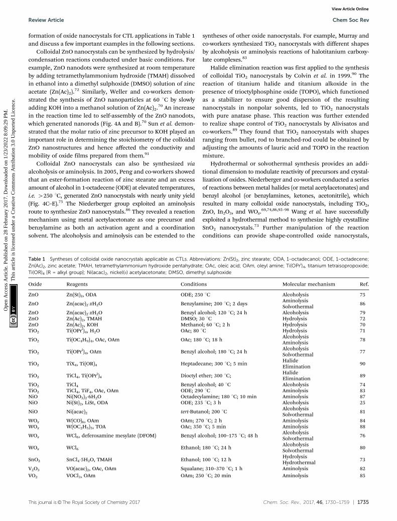
formation of oxide nanocrystals for CTL applications in Table 1and discuss a few important examples in the following sections.
Colloidal ZnO nanocrystals can be synthesized by hydrolysis/condensation reactions conducted under basic conditions. Forexample, ZnO nanodots were synthesized at room temperatureby adding tetramethylammonium hydroxide (TMAH) dissolvedin ethanol into a dimethyl sulphoxide (DMSO) solution of zincacetate (Zn(Ac)2).72 Similarly, Weller and co-workers demon-strated the synthesis of ZnO nanoparticles at 60 1C by slowlyadding KOH into a methanol solution of Zn(Ac)2.70 An increasein the reaction time led to self-assembly of the ZnO nanodots,which generated nanorods (Fig. 4A and B).70 Sun et al. demon-strated that the molar ratio of zinc precursor to KOH played animportant role in determining the stoichiometry of the colloidalZnO nanostructures and hence affected the conductivity andmobility of oxide films prepared from them.91
Colloidal ZnO nanocrystals can also be synthesized viaalcoholysis or aminolysis. In 2005, Peng and co-workers showedthat an ester-formation reaction of zinc stearate and an excessamount of alcohol in 1-octadecene (ODE) at elevated temperatures,i.e. 4250 1C, generated ZnO nanocrystals with nearly unity yield(Fig. 4C–E).75 The Niederberger group exploited an aminolysisroute to synthesize ZnO nanocrystals.86 They revealed a reactionmechanism using metal acetylacetonate as one precursor andbenzylamine as both an activation agent and a coordinationsolvent. The alcoholysis and aminolysis can be extended to the
syntheses of other oxide nanocrystals. For example, Murray andco-workers synthesized TiO2 nanocrystals with different shapesby alcoholysis or aminolysis reactions of halotitanium carboxy-late complexes.83
Halide elimination reaction was first applied to the synthesisof colloidal TiO2 nanocrystals by Colvin et al. in 1999.90 Thereaction of titanium halide and titanium alkoxide in thepresence of trioctylphosphine oxide (TOPO), which functionedas a stabilizer to ensure good dispersion of the resultingnanocrystals in nonpolar solvents, led to TiO2 nanocrystalswith pure anatase phase. This reaction was further extendedto realize shape control of TiO2 nanocrystals by Alivisatos andco-workers.89 They found that TiO2 nanocrystals with shapesranging from bullet, rod to branched-rod could be obtained byadjusting the amounts of lauric acid and TOPO in the reactionmixture.
Hydrothermal or solvothermal synthesis provides an addi-tional dimension to modulate reactivity of precursors and crystal-lization of oxides. Niederberger and co-workers conducted a seriesof reactions between metal halides (or metal acetylacetonates) andbenzyl alcohol (or benzylamines, ketones, acetonitrile), whichresulted in many colloidal oxide nanocrystals, including TiO2,ZnO, In2O3, and WOx.69,74,86,92–98 Wang et al. have successfullyexploited a hydrothermal method to synthesize highly crystallineSnO2 nanocrystals.73 Further manipulation of the reactionconditions can provide shape-controlled oxide nanocrystals,
Table 1 Syntheses of colloidal oxide nanocrystals applicable as CTLs. Abbreviations: Zn(St)2, zinc stearate; ODA, 1-octadecanol; ODE, 1-octadecene;Zn(Ac)2, zinc acetate; TMAH, tetramethylammonium hydroxide pentahydrate; OAc, oleic acid; OAm, oleyl amine; Ti(OPri)4, titanium tetraisopropoxide;Ti(OR)4 [R = alkyl group]; Ni(acac)2, nickel(II) acetylacetonate; DMSO, dimethyl sulphoxide
Oxide Reagents Conditions Molecular mechanism Ref.
ZnO Zn(St)2, ODA ODE; 250 1C Alcoholysis 75
ZnO Zn(acac)2�xH2O Benzylamine; 200 1C; 2 days Aminolysis 86SolvothermalZnO Zn(acac)2�xH2O Benzyl alcohol; 120 1C; 24 h Alcoholysis 79ZnO Zn(Ac)2, TMAH DMSO; 30 1C Hydrolysis 72ZnO Zn(Ac)2, KOH Methanol; 60 1C; 2 h Hydrolysis 70TiO2 Ti(OPri)4, H2O OAc; 80 1C Hydrolysis 71
TiO2 Ti(OC4H9)4, OAc, OAm OAc; 180 1C; 18 h Alcoholysis 78Aminolysis
TiO2 Ti(OPri)4, OAm Benzyl alcohol; 180 1C; 24 h Alcoholysis 77Solvothermal
TiO2 TiX4, Ti(OR)4 Heptadecane; 300 1C; 5 min Halide 90Elimination
TiO2 TiCl4, Ti(OPri)4 Dioctyl ether; 300 1C; Halide 89EliminationTiO2 TiCl4 Benzyl alcohol; 40 1C Alcoholysis 74TiO2 TiCl4, TiF4, OAc, OAm ODE; 290 1C Aminolysis 83NiO Ni(NO3)2�6H2O Octadecylamine; 180 1C; 10 min Aminolysis 87NiO Ni(St)2, LiSt, ODA ODE; 235 1C; 3 h Alcoholysis 25
NiO Ni(acac)2 tert-Butanol; 200 1C Alcoholysis 81SolvothermalWOx W(CO)6, OAm OAm; 270 1C; 2 h Aminolysis 84WOx W(OC2H5)5, TOA OAc; 350 1C; 5 min Aminolysis 88
WOx WCl6, deferoxamine mesylate (DFOM) Benzyl alcohol; 100–175 1C; 48 h Alcoholysis 76Solvothermal
WOx WCl6 Ethanol; 180 1C; 24 h Alcoholysis 80Solvothermal
SnO2 SnCl4�5H2O, TMAH Ethanol; 100 1C; 12 h Hydrolysis 73HydrothermalV2O3 VO(acac)2, OAc, OAm Squalane; 310–370 1C; 1 h Aminolysis 82VO2 VOCl3, OAm OAm; 250 1C; 20 min Aminolysis 85
Review Article Chem Soc Rev
Ope
n A
cces
s A
rtic
le. P
ublis
hed
on 2
8 Fe
brua
ry 2
017.
Dow
nloa
ded
on 1
/23/
2022
8:0
9:29
PM
. T
his
artic
le is
lice
nsed
und
er a
Cre
ativ
e C
omm
ons
Attr
ibut
ion
3.0
Unp
orte
d L
icen
ce.
View Article Online

1736 | Chem. Soc. Rev., 2017, 46, 1730--1759 This journal is©The Royal Society of Chemistry 2017
such as colloidal TiO2 nanosheets and rhombic TiO2 nanocrystalswith exposed high-energy facets.77
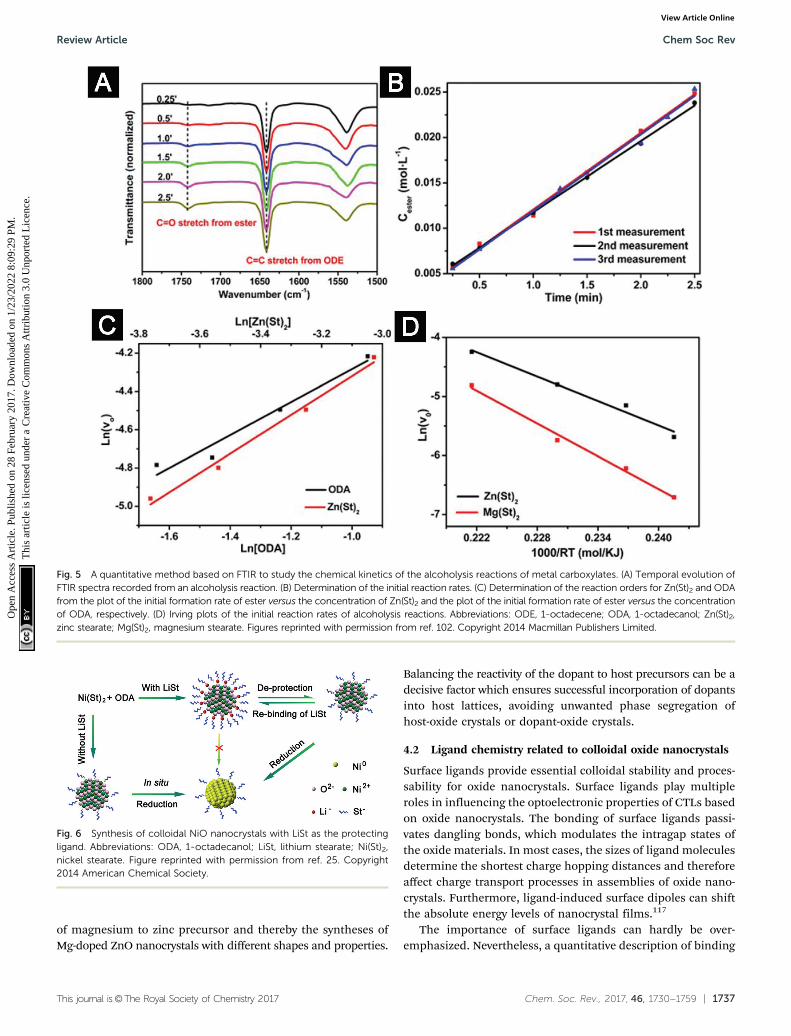
Identifying molecular pathways and quantifying chemicalkinetics can provide valuable information to understand thechemical reactions associated with the formation of oxidenanocrystals. This can be done by tracing the organic by-products.For example, by-products of alcoholysis and hydrolysis reactionsof metal carboxylates are ester and acid, respectively, which showdistinctly different absorption features in the Fourier transforminfrared spectroscopy (FTIR).99,100 We carried out a series oftemperature-dependent FTIR measurements on a variety ofmetal carboxylates.100,101 The results inspired us to controlreaction pathways by modifying experimental procedures andselecting metal precursors with adequate reactivity. Furthermore,we developed an experimental method based on FTIR to measurethe initial reaction rates of the alcoholysis reactions of metalcarboxylates (Fig. 5).102 This method allowed us to quantitativelycompare reactivity of different metal precursors under givenreaction conditions and obtain important kinetic parameters,such as activation energy. In another report, Niederberger andco-workers investigated the molecular mechanism and crystal-lization of ZnO nanocrystals synthesized by the benzyl alcoholroute.79 They used gas chromatography to quantify the organicby-products and concluded that the rate-limiting step forthe formation of ZnO nanocrystals was the generation of themonomer species.
Mechanistic understanding at the molecular level is beneficialfor rational design of synthetic chemistry of colloidal oxidenanocrystals. For example, we identified that the synthesis ofpure colloidal NiO nanocrystals by alcoholysis of metal carboxy-lates was plagued by an unwanted side reaction, in situ reductionof NiO nanocrystals by alcohol at elevated temperatures.25 In thisregard, we introduced lithium stearate, an ionic molecule whichis stable in the reaction system and capable of binding ontothe surface of NiO nanocrystals to suppress their reactivity.This ligand-protection strategy (Fig. 6) prevented the reduction
reactions, leading to pure and high-quality NiO nanocrystalswith a high yield.
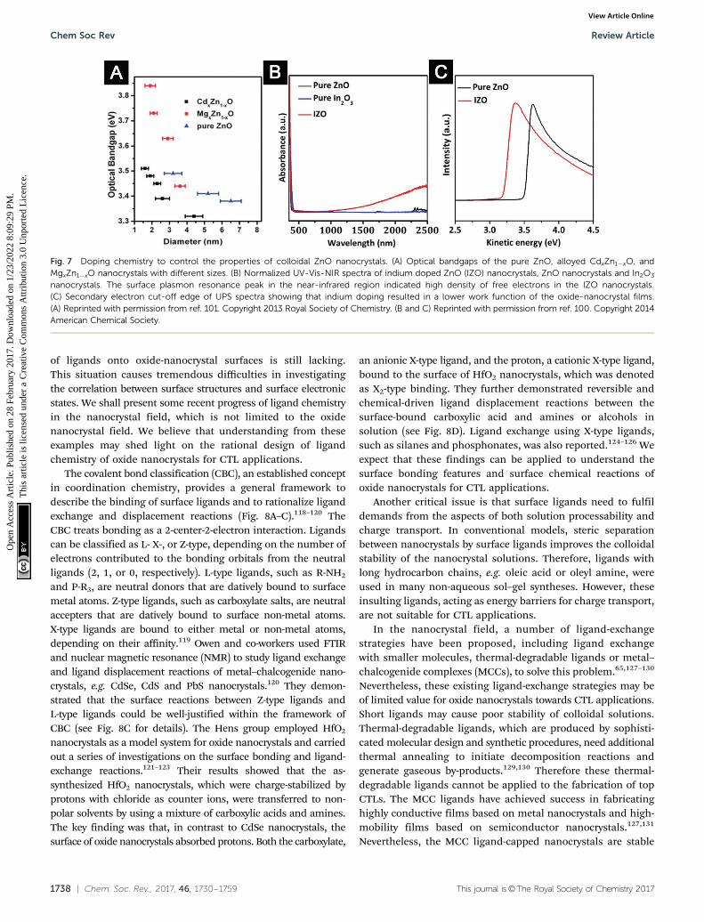
Knowledge of molecular mechanisms and reaction kineticsis critical for controlled doping of oxide nanocrystals. Introductionof specific dopants is a general approach to modify the propertiesof nanocrystals in well-controlled ways. Isovalent doping, i.e.alloying, can modulate the bandgap energy of nanocrystals.72,99
Our group demonstrated the syntheses of Mg-doped ZnO nano-crystals and Cd-doped ZnO nanocrystals with tuneable opticalbandgaps ranging from 3.3 to 3.9 eV (Fig. 7A).99,101 We discoveredinteresting dopant induced shape evolution for these doped oxidenanocrystals, which was later observed in many other dopedcolloidal nanocrystal systems.103–105 Aliovalent doping can generateadditional free carriers in oxide nanocrystals,100,106–113 which maylead to enhanced conductivity and modified work function of thefilms processed from the doped oxide nanocrystals (Fig. 7B and C).Typical examples are ZnO nanocrystals doped with group IIIelements of Al3+, Ga3+ or In3+,106–112 and TiO2 nanocrystals dopedwith Nb5+.114,115 At the molecular level, successful doping of oxidenanocrystals is likely to be a result of in situ incorporation of thedopant ions during the growth of the host oxide nanocrystals. A keyissue linking chemical reactions and crystallization processes ofdoped oxide nanocrystals is that adequate host crystal growth anddopant incorporation rates rely on balanced host–dopant precursorreactivity.116 Milliron and co-workers found that for the synthesisof Al-doped ZnO nanocrystals, successful doping was achievedwhen zinc stearate and aluminium acetylacetonate were selected asprecursors.106 No doping was observed when the dopant precursorwas replaced by the less reactive aluminium stearate. Our groupemployed the synthesis of Mg-doped ZnO nanocrystals as a modelsystem to quantitatively study the correlation between chemicalkinetics of the precursor conversion reactions and formation ofdoped nanocrystals under synthetic conditions.102 The resultsshowed that three independent factors, molar ratio of thedopant precursor, reaction temperature and coordinationligands of cationic precursors, influenced the relative reactivity
Fig. 4 (A and B) Colloidal ZnO nanocrystals synthesized by the hydrolysis approach. Typical TEM images of (A) ZnO nanodots and (B) ZnO nanorods(grown by the self-assembly of nanodots). (C–E) Colloidal ZnO nanocrystals synthesized by the alcoholysis approach. (C) Reagents and reactionconditions. (D) FTIR spectra to reveal the molecular mechanism. (E) A typical TEM image of the ZnO nanocrystals. (A and B) Reprinted with permissionfrom ref. 70. Copyright 2002 Wiley-VCH. (C–E) Adapted with permission from ref. 75. Copyright 2005 American Chemical Society.
Chem Soc Rev Review Article
Ope
n A
cces
s A
rtic
le. P
ublis
hed
on 2
8 Fe
brua
ry 2
017.
Dow
nloa
ded
on 1
/23/
2022
8:0
9:29
PM
. T
his
artic
le is
lice
nsed
und
er a
Cre
ativ
e C
omm
ons
Attr
ibut
ion
3.0
Unp
orte
d L
icen
ce.
View Article Online
This journal is©The Royal Society of Chemistry 2017 Chem. Soc. Rev., 2017, 46, 1730--1759 | 1737
of magnesium to zinc precursor and thereby the syntheses ofMg-doped ZnO nanocrystals with different shapes and properties.
Balancing the reactivity of the dopant to host precursors can be adecisive factor which ensures successful incorporation of dopantsinto host lattices, avoiding unwanted phase segregation ofhost-oxide crystals or dopant-oxide crystals.
4.2 Ligand chemistry related to colloidal oxide nanocrystals
Surface ligands provide essential colloidal stability and proces-sability for oxide nanocrystals. Surface ligands play multipleroles in influencing the optoelectronic properties of CTLs basedon oxide nanocrystals. The bonding of surface ligands passi-vates dangling bonds, which modulates the intragap states ofthe oxide materials. In most cases, the sizes of ligand moleculesdetermine the shortest charge hopping distances and thereforeaffect charge transport processes in assemblies of oxide nano-crystals. Furthermore, ligand-induced surface dipoles can shiftthe absolute energy levels of nanocrystal films.117
The importance of surface ligands can hardly be over-emphasized. Nevertheless, a quantitative description of binding
Fig. 5 A quantitative method based on FTIR to study the chemical kinetics of the alcoholysis reactions of metal carboxylates. (A) Temporal evolution ofFTIR spectra recorded from an alcoholysis reaction. (B) Determination of the initial reaction rates. (C) Determination of the reaction orders for Zn(St)2 and ODAfrom the plot of the initial formation rate of ester versus the concentration of Zn(St)2 and the plot of the initial formation rate of ester versus the concentrationof ODA, respectively. (D) Irving plots of the initial reaction rates of alcoholysis reactions. Abbreviations: ODE, 1-octadecene; ODA, 1-octadecanol; Zn(St)2,zinc stearate; Mg(St)2, magnesium stearate. Figures reprinted with permission from ref. 102. Copyright 2014 Macmillan Publishers Limited.
Fig. 6 Synthesis of colloidal NiO nanocrystals with LiSt as the protectingligand. Abbreviations: ODA, 1-octadecanol; LiSt, lithium stearate; Ni(St)2,nickel stearate. Figure reprinted with permission from ref. 25. Copyright2014 American Chemical Society.
Review Article Chem Soc Rev
Ope
n A
cces
s A
rtic
le. P
ublis
hed
on 2
8 Fe
brua
ry 2
017.
Dow
nloa
ded
on 1
/23/
2022
8:0
9:29
PM
. T
his
artic
le is
lice
nsed
und
er a
Cre
ativ
e C
omm
ons
Attr
ibut
ion
3.0
Unp
orte
d L
icen
ce.
View Article Online
1738 | Chem. Soc. Rev., 2017, 46, 1730--1759 This journal is©The Royal Society of Chemistry 2017
of ligands onto oxide-nanocrystal surfaces is still lacking.This situation causes tremendous difficulties in investigatingthe correlation between surface structures and surface electronicstates. We shall present some recent progress of ligand chemistryin the nanocrystal field, which is not limited to the oxidenanocrystal field. We believe that understanding from theseexamples may shed light on the rational design of ligandchemistry of oxide nanocrystals for CTL applications.
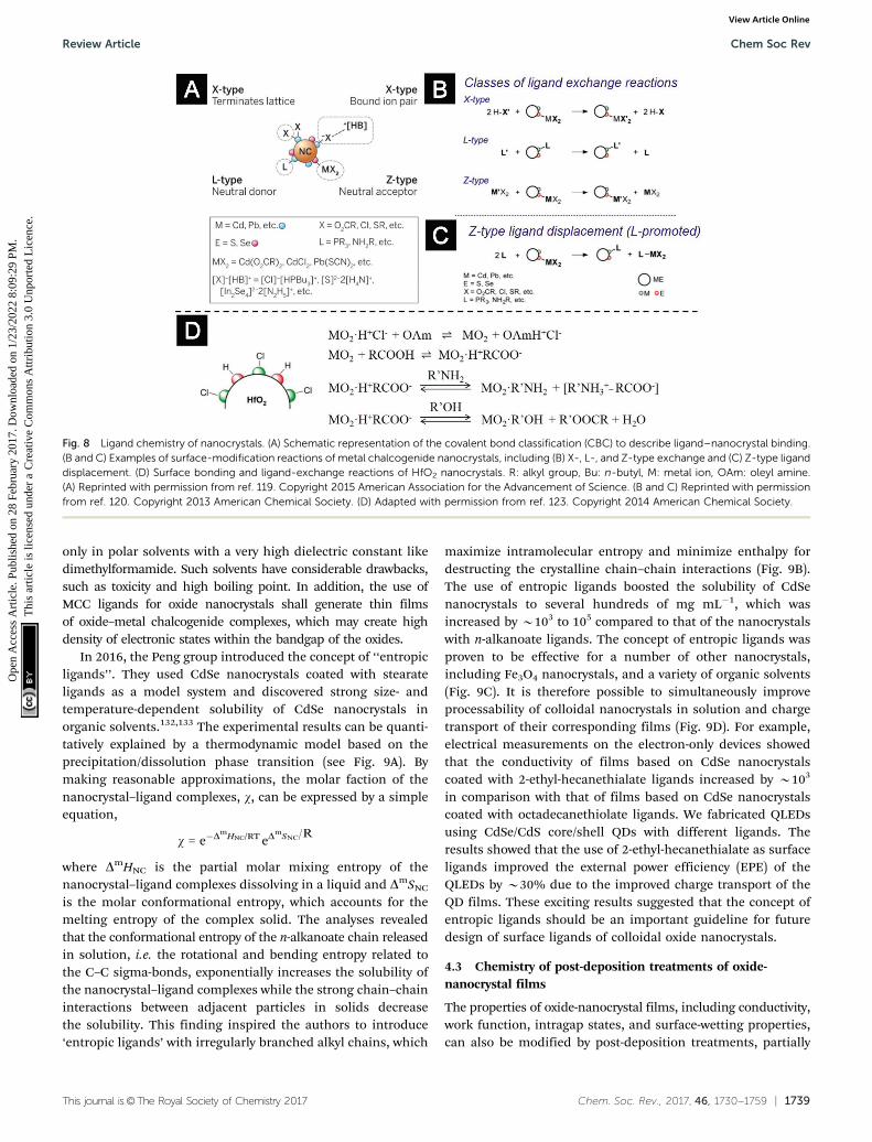
The covalent bond classification (CBC), an established conceptin coordination chemistry, provides a general framework todescribe the binding of surface ligands and to rationalize ligandexchange and displacement reactions (Fig. 8A–C).118–120 TheCBC treats bonding as a 2-center-2-electron interaction. Ligandscan be classified as L- X-, or Z-type, depending on the number ofelectrons contributed to the bonding orbitals from the neutralligands (2, 1, or 0, respectively). L-type ligands, such as R-NH2
and P-R3, are neutral donors that are datively bound to surfacemetal atoms. Z-type ligands, such as carboxylate salts, are neutralaccepters that are datively bound to surface non-metal atoms.X-type ligands are bound to either metal or non-metal atoms,depending on their affinity.119 Owen and co-workers used FTIRand nuclear magnetic resonance (NMR) to study ligand exchangeand ligand displacement reactions of metal–chalcogenide nano-crystals, e.g. CdSe, CdS and PbS nanocrystals.120 They demon-strated that the surface reactions between Z-type ligands andL-type ligands could be well-justified within the framework ofCBC (see Fig. 8C for details). The Hens group employed HfO2
nanocrystals as a model system for oxide nanocrystals and carriedout a series of investigations on the surface bonding and ligand-exchange reactions.121–123 Their results showed that the as-synthesized HfO2 nanocrystals, which were charge-stabilized byprotons with chloride as counter ions, were transferred to non-polar solvents by using a mixture of carboxylic acids and amines.The key finding was that, in contrast to CdSe nanocrystals, thesurface of oxide nanocrystals absorbed protons. Both the carboxylate,
an anionic X-type ligand, and the proton, a cationic X-type ligand,bound to the surface of HfO2 nanocrystals, which was denotedas X2-type binding. They further demonstrated reversible andchemical-driven ligand displacement reactions between thesurface-bound carboxylic acid and amines or alcohols insolution (see Fig. 8D). Ligand exchange using X-type ligands,such as silanes and phosphonates, was also reported.124–126 Weexpect that these findings can be applied to understand thesurface bonding features and surface chemical reactions ofoxide nanocrystals for CTL applications.
Another critical issue is that surface ligands need to fulfildemands from the aspects of both solution processability andcharge transport. In conventional models, steric separationbetween nanocrystals by surface ligands improves the colloidalstability of the nanocrystal solutions. Therefore, ligands withlong hydrocarbon chains, e.g. oleic acid or oleyl amine, wereused in many non-aqueous sol–gel syntheses. However, theseinsulting ligands, acting as energy barriers for charge transport,are not suitable for CTL applications.
In the nanocrystal field, a number of ligand-exchangestrategies have been proposed, including ligand exchangewith smaller molecules, thermal-degradable ligands or metal–chalcogenide complexes (MCCs), to solve this problem.65,127–130
Nevertheless, these existing ligand-exchange strategies may beof limited value for oxide nanocrystals towards CTL applications.Short ligands may cause poor stability of colloidal solutions.Thermal-degradable ligands, which are produced by sophisti-cated molecular design and synthetic procedures, need additionalthermal annealing to initiate decomposition reactions andgenerate gaseous by-products.129,130 Therefore these thermal-degradable ligands cannot be applied to the fabrication of topCTLs. The MCC ligands have achieved success in fabricatinghighly conductive films based on metal nanocrystals and high-mobility films based on semiconductor nanocrystals.127,131
Nevertheless, the MCC ligand-capped nanocrystals are stable
Fig. 7 Doping chemistry to control the properties of colloidal ZnO nanocrystals. (A) Optical bandgaps of the pure ZnO, alloyed CdxZn1�xO, andMgxZn1�xO nanocrystals with different sizes. (B) Normalized UV-Vis-NIR spectra of indium doped ZnO (IZO) nanocrystals, ZnO nanocrystals and In2O3
nanocrystals. The surface plasmon resonance peak in the near-infrared region indicated high density of free electrons in the IZO nanocrystals.(C) Secondary electron cut-off edge of UPS spectra showing that indium doping resulted in a lower work function of the oxide-nanocrystal films.(A) Reprinted with permission from ref. 101. Copyright 2013 Royal Society of Chemistry. (B and C) Reprinted with permission from ref. 100. Copyright 2014American Chemical Society.
Chem Soc Rev Review Article
Ope
n A
cces
s A
rtic
le. P
ublis
hed
on 2
8 Fe
brua
ry 2
017.
Dow
nloa
ded
on 1
/23/
2022
8:0
9:29
PM
. T
his
artic
le is
lice
nsed
und
er a
Cre
ativ
e C
omm
ons
Attr
ibut
ion
3.0
Unp
orte
d L
icen
ce.
View Article Online
This journal is©The Royal Society of Chemistry 2017 Chem. Soc. Rev., 2017, 46, 1730--1759 | 1739
only in polar solvents with a very high dielectric constant likedimethylformamide. Such solvents have considerable drawbacks,such as toxicity and high boiling point. In addition, the use ofMCC ligands for oxide nanocrystals shall generate thin filmsof oxide–metal chalcogenide complexes, which may create highdensity of electronic states within the bandgap of the oxides.
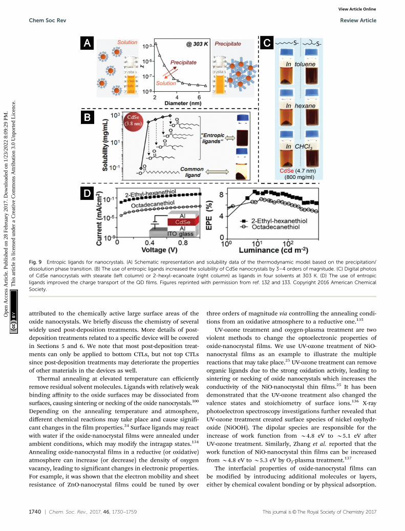
In 2016, the Peng group introduced the concept of ‘‘entropicligands’’. They used CdSe nanocrystals coated with stearateligands as a model system and discovered strong size- andtemperature-dependent solubility of CdSe nanocrystals inorganic solvents.132,133 The experimental results can be quanti-tatively explained by a thermodynamic model based on theprecipitation/dissolution phase transition (see Fig. 9A). Bymaking reasonable approximations, the molar faction of thenanocrystal–ligand complexes, w, can be expressed by a simpleequation,
w = e�DmHNC/RT eD
mSNC/R
where DmHNC is the partial molar mixing entropy of thenanocrystal–ligand complexes dissolving in a liquid and DmSNC
is the molar conformational entropy, which accounts for themelting entropy of the complex solid. The analyses revealedthat the conformational entropy of the n-alkanoate chain releasedin solution, i.e. the rotational and bending entropy related tothe C–C sigma-bonds, exponentially increases the solubility ofthe nanocrystal–ligand complexes while the strong chain–chaininteractions between adjacent particles in solids decreasethe solubility. This finding inspired the authors to introduce‘entropic ligands’ with irregularly branched alkyl chains, which
maximize intramolecular entropy and minimize enthalpy fordestructing the crystalline chain–chain interactions (Fig. 9B).The use of entropic ligands boosted the solubility of CdSenanocrystals to several hundreds of mg mL�1, which wasincreased by B103 to 105 compared to that of the nanocrystalswith n-alkanoate ligands. The concept of entropic ligands wasproven to be effective for a number of other nanocrystals,including Fe3O4 nanocrystals, and a variety of organic solvents(Fig. 9C). It is therefore possible to simultaneously improveprocessability of colloidal nanocrystals in solution and chargetransport of their corresponding films (Fig. 9D). For example,electrical measurements on the electron-only devices showedthat the conductivity of films based on CdSe nanocrystalscoated with 2-ethyl-hecanethialate ligands increased by B103
in comparison with that of films based on CdSe nanocrystalscoated with octadecanethiolate ligands. We fabricated QLEDsusing CdSe/CdS core/shell QDs with different ligands. Theresults showed that the use of 2-ethyl-hecanethialate as surfaceligands improved the external power efficiency (EPE) of theQLEDs by B30% due to the improved charge transport of theQD films. These exciting results suggested that the concept ofentropic ligands should be an important guideline for futuredesign of surface ligands of colloidal oxide nanocrystals.
4.3 Chemistry of post-deposition treatments of oxide-nanocrystal films
The properties of oxide-nanocrystal films, including conductivity,work function, intragap states, and surface-wetting properties,can also be modified by post-deposition treatments, partially
Fig. 8 Ligand chemistry of nanocrystals. (A) Schematic representation of the covalent bond classification (CBC) to describe ligand–nanocrystal binding.(B and C) Examples of surface-modification reactions of metal chalcogenide nanocrystals, including (B) X-, L-, and Z-type exchange and (C) Z-type liganddisplacement. (D) Surface bonding and ligand-exchange reactions of HfO2 nanocrystals. R: alkyl group, Bu: n-butyl, M: metal ion, OAm: oleyl amine.(A) Reprinted with permission from ref. 119. Copyright 2015 American Association for the Advancement of Science. (B and C) Reprinted with permissionfrom ref. 120. Copyright 2013 American Chemical Society. (D) Adapted with permission from ref. 123. Copyright 2014 American Chemical Society.
Review Article Chem Soc Rev
Ope
n A
cces
s A
rtic
le. P
ublis
hed
on 2
8 Fe
brua
ry 2
017.
Dow
nloa
ded
on 1
/23/
2022
8:0
9:29
PM
. T
his
artic
le is
lice
nsed
und
er a
Cre
ativ
e C
omm
ons
Attr
ibut
ion
3.0
Unp
orte
d L
icen
ce.
View Article Online
1740 | Chem. Soc. Rev., 2017, 46, 1730--1759 This journal is©The Royal Society of Chemistry 2017
attributed to the chemically active large surface areas of theoxide nanocrystals. We briefly discuss the chemistry of severalwidely used post-deposition treatments. More details of post-deposition treatments related to a specific device will be coveredin Sections 5 and 6. We note that most post-deposition treat-ments can only be applied to bottom CTLs, but not top CTLssince post-deposition treatments may deteriorate the propertiesof other materials in the devices as well.
Thermal annealing at elevated temperature can efficientlyremove residual solvent molecules. Ligands with relatively weakbinding affinity to the oxide surfaces may be dissociated fromsurfaces, causing sintering or necking of the oxide nanocrystals.100
Depending on the annealing temperature and atmosphere,different chemical reactions may take place and cause signifi-cant changes in the film properties.24 Surface ligands may reactwith water if the oxide-nanocrystal films were annealed underambient conditions, which may modify the intragap states.134
Annealing oxide-nanocrystal films in a reductive (or oxidative)atmosphere can increase (or decrease) the density of oxygenvacancy, leading to significant changes in electronic properties.For example, it was shown that the electron mobility and sheetresistance of ZnO-nanocrystal films could be tuned by over
three orders of magnitude via controlling the annealing condi-tions from an oxidative atmosphere to a reductive one.135
UV-ozone treatment and oxygen-plasma treatment are twoviolent methods to change the optoelectronic properties ofoxide-nanocrystal films. We use UV-ozone treatment of NiO-nanocrystal films as an example to illustrate the multiplereactions that may take place.25 UV-ozone treatment can removeorganic ligands due to the strong oxidation activity, leading tosintering or necking of oxide nanocrystals which increases theconductivity of the NiO-nanocrystal thin films.25 It has beendemonstrated that the UV-ozone treatment also changed thevalence states and stoichiometry of surface ions.136 X-rayphotoelectron spectroscopy investigations further revealed thatUV-ozone treatment created surface species of nickel oxyhydr-oxide (NiOOH). The dipolar species are responsible for theincrease of work function from B4.8 eV to B5.1 eV afterUV-ozone treatment. Similarly, Zhang et al. reported that thework function of NiO-nanocrystal thin films can be increasedfrom B4.8 eV to B5.3 eV by O2-plasma treatment.137
The interfacial properties of oxide-nanocrystal films canbe modified by introducing additional molecules or layers,either by chemical covalent bonding or by physical adsorption.
Fig. 9 Entropic ligands for nanocrystals. (A) Schematic representation and solubility data of the thermodynamic model based on the precipitation/dissolution phase transition. (B) The use of entropic ligands increased the solubility of CdSe nanocrystals by 3–4 orders of magnitude. (C) Digital photosof CdSe nanocrystals with stearate (left column) or 2-hexyl-ecanoate (right column) as ligands in four solvents at 303 K. (D) The use of entropicligands improved the charge transport of the QD films. Figures reprinted with permission from ref. 132 and 133. Copyright 2016 American ChemicalSociety.
Chem Soc Rev Review Article
Ope
n A
cces
s A
rtic
le. P
ublis
hed
on 2
8 Fe
brua
ry 2
017.
Dow
nloa
ded
on 1
/23/
2022
8:0
9:29
PM
. T
his
artic
le is
lice
nsed
und
er a
Cre
ativ
e C
omm
ons
Attr
ibut
ion
3.0
Unp
orte
d L
icen
ce.
View Article Online

This journal is©The Royal Society of Chemistry 2017 Chem. Soc. Rev., 2017, 46, 1730--1759 | 1741
Polyethylenimine ethoxylated (PEIE) or branched polyethylenimine(PEI) are polymers containing simple aliphatic amine groups.Physisorption of an ultrathin layer of these polymers onto thesurfaces of oxide-nanocrystal films induced interfacial dipoles,which reduced the work function of the oxide-nanocrystalfilms, as revealed by ultraviolet photoemission spectroscopy(UPS) and Kelvin probe measurements.138 The modification ofsurface work function can also be realized by using covalentlybonded self-assembled monolayers (SAMs). For example, thework function of ZnO films can be controlled by a SAM ofmolecules derived from benzoic acid derivatives with differentdipole orientations.139 The covalent bonding of additionalmolecules onto the surfaces of oxide nanocrystals can effi-ciently modulate the intragap states of the films. We developeda simple passivation method based on ethanedithiol (EDT)treatment for ZnO-nanocrystal films (Fig. 10).19 The surfacedefects of the ZnO-nanocrystal films including surface groups,such as hydroxyl groups and carboxylate groups, and danglingbonds were removed by forming zinc ethanedithiolates, whichintroduced a new intragap band.
5. Recent developments of CTLsbased on colloidal oxide nanocrystalsfor solution-processed LEDs5.1 Solution-processed organic LEDs (OLEDs)
Electroluminescence from conjugated polymers was first demon-strated in 1990, using poly(p-phenylene vinylene) (PPV) as a singlesemiconductor layer sandwiched between metallic electrodes.1
Since then, solution-processed OLEDs have experienced signifi-cant advances in the past B25 years. Intensive work on syntheticchemistry, together with new understanding on photo-physics,has now led to many solution-processed organic materials withgood emissive properties, including polymers, dendrimers andsmall molecules.140–144 Innovations on device architectures andthe corresponding CTLs were made to optimize charge balanceand achieve long operational lifetime.
In the early stages, poor electron injection was one of thelimiting factors for solution-processed OLEDs due to the relativelyhigh energy offset between the lowest-unoccupied-molecular-orbital (LUMO) energy levels of organic emitters and the Fermilevels of electrodes. Metals with low work function, such as Caor Ba, were used to facilitate electron injection into organiclayers. However, these low-work-function metals and the inter-faces of polymer/metal are unstable, resulting in poor devicestability. Furthermore, the most widely used hole injectionmaterial, poly(3,4-ethylenedioxythiophene)-poly(styrene sulfonate)(PEDOT:PSS), suffers from hygroscopicity and acidic nature.These facts inspired scientists to introduce solution-processedoxides as CTLs for organic LEDs.141,145 Here we focus on theapplications of colloidal oxide nanocrystals as CTLs in solution-processed OLEDs.
Haque and co-workers introduced nanocrystalline TiO2
thin films as ETLs for polymer LEDs in 2007.146 Although theefficiency of this device was modest, the device performancewas enhanced compared with the devices without TiO2 ETLs.Qian et al. applied ZnO-nanocrystal ETLs in polymer LEDswith poly[2-methoxy-5-(2-ethylhexyloxy)-1,phenylene vinylene](MEH-PPV) emitters.147 Sessolo et al. employed ZnO nanocrystalsas ETLs in flexible polymer LEDs on plastic substrates, leading tovery bright poly(9,9-dioctylfluorene-alt-benzothiadiazole) (F8BT)electroluminescence.148 The turn-on voltages of the devices usingZnO-nanocrystal ETLs are lower than the corresponding energygaps of the luminescent materials, indicating efficient electroninjection. The Auger assisted energy up-conversion process occur-ring at the polymer/ZnO nanocrystal interface was invoked toexplain this sub-bandgap turn-on phenomenon.147 This mecha-nism is plausible. Sub-bandgap turn-on at room temperature wascommonly observed for the vacuum-deposited high-efficiencyinorganic LEDs with ohmic contacts.149
The performance of solution-processed OLEDs can be optimizedby tuning the properties of oxide-nanocrystal ETLs. Here we selecteda few examples of LEDs using F8BT as an emissive material andZnO nanocrystals as ETLs to highlight the importance of controllingthe interface of emissive organics/oxide nanocrystals.100,150,151
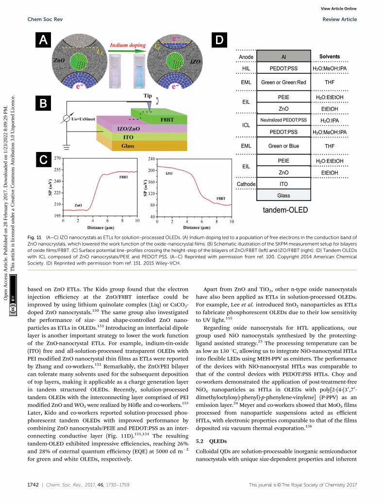
In general, an energy barrier for electron injection exists at theZnO/F8BT interface. This electron injection barrier can bemodulated by adjusting the work function of the ZnO ETLs.Our group synthesized indium-doped ZnO (IZO) nanocrystalswith high density of free carriers. The indium doping accom-panied by filling free electrons into the conduction bandgenerated an up-shift of B0.3 eV in the Fermi level of the oxideETLs (Fig. 11A).100 Scanning Kelvin probe microscopy (SKPM)results on the bilayers of F8BT/IZO nanocrystal thin filmsshowed that the surface potential of the IZO-nanocrystal layerwas more positive than that of the F8BT layer, while in the caseof the F8BT/ZnO nanocrystal bilayer, the surface potential ofthe ZnO-nanocrystal layer was more negative than that of theF8BT layer (Fig. 11B and C). Therefore, the IZO-nanocrystalETLs offered improved efficient injection properties. As aresult, the PLEDs based on IZO ETLs exhibited much betterperformance, i.e. lower turn-on voltages, higher maximumluminance and higher efficiency, compared with the devices
Fig. 10 Modulation of the intragap states of the ZnO-nanocrystal films byEDT treatment. Figure adapted with permission from ref. 19. Copyright2014 Wiley-VCH.
Review Article Chem Soc Rev
Ope
n A
cces
s A
rtic
le. P
ublis
hed
on 2
8 Fe
brua
ry 2
017.
Dow
nloa
ded
on 1
/23/
2022
8:0
9:29
PM
. T
his
artic
le is
lice
nsed
und
er a
Cre
ativ
e C
omm
ons
Attr
ibut
ion
3.0
Unp
orte
d L
icen
ce.
View Article Online
1742 | Chem. Soc. Rev., 2017, 46, 1730--1759 This journal is©The Royal Society of Chemistry 2017
based on ZnO ETLs. The Kido group found that the electroninjection efficiency at the ZnO/F8BT interface could beimproved by using lithium quinolate complex (Liq) or CsCO3-doped ZnO nanocrystals.150 The same group also investigatedthe performance of size- and shape-controlled ZnO nano-particles as ETLs in OLEDs.151 Introducing an interfacial dipolelayer is another important strategy to lower the work functionof the ZnO-nanocrystal ETLs. For example, indium-tin-oxide(ITO) free and all-solution-processed transparent OLEDs withPEI modified ZnO nanocrystal thin films as ETLs were reportedby Zhang and co-workers.152 Remarkably, the ZnO/PEI bilayercan tolerate many solvents used for the subsequent depositionof top layers, making it applicable as a charge generation layerin tandem structured OLEDs. Recently, solution-processedtandem OLEDs with the interconnecting layer comprised of PEImodified ZnO and WO3 were realized by Hofle and co-workers.153
Later, Kido and co-workers reported solution-processed phos-phorescent tandem OLEDs with improved performance bycombining ZnO nanocrystals/PEIE and PEDOT:PSS as an inter-connecting conductive layer (Fig. 11D).151,154 The resultingtandem-OLED exhibited impressive efficiencies, reaching 26%and 28% of external quantum efficiency (EQE) at 5000 cd m�2
for green and white OLEDs, respectively.
Apart from ZnO and TiO2, other n-type oxide nanocrystalshave also been applied as ETLs in solution-processed OLEDs.For example, Lee et al. introduced SnO2 nanoparticles as ETLsto fabricate phosphorescent OLEDs due to their low sensitivityto UV light.155
Regarding oxide nanocrystals for HTL applications, ourgroup used NiO nanocrystals synthesized by the protecting-ligand assisted strategy.25 The processing temperature can beas low as 130 1C, allowing us to integrate NiO-nanocrystal HTLsinto flexible LEDs using MEH-PPV as emitters. The performanceof the devices with NiO-nanocrystal HTLs was comparable tothat of the control devices with PEDOT:PSS HTLs. Choy andco-workers demonstrated the application of post-treatment-freeNiOx nanoparticles as HTLs in OLEDs with poly[2-(4-(30,70-dimethyloctyloxy)-phenyl)-p-phenylene-vinylene] (P-PPV) as anemission layer.24 Meyer and co-workers showed that MoO3 filmsprocessed from nanoparticle suspensions acted as efficientHTLs, with electronic properties comparable to that of the filmsdeposited via vacuum thermal evaporation.156
5.2 QLEDs
Colloidal QDs are solution-processable inorganic semiconductornanocrystals with unique size-dependent properties and inherent
Fig. 11 (A–C) IZO nanocrystals as ETLs for solution-processed OLEDs. (A) Indium doping led to a population of free electrons in the conduction band ofZnO nanocrystals, which lowered the work function of the oxide-nanocrystal films. (B) Schematic illustration of the SKPM measurement setup for bilayersof oxide films/F8BT. (C) Surface potential line-profiles crossing the height-step of the bilayers of ZnO/F8BT (left) and IZO/F8BT (right). (D) Tandem OLEDswith ICL composed of ZnO nanocrystals/PEIE and PEDOT:PSS. (A–C) Reprinted with permission from ref. 100. Copyright 2014 American ChemicalSociety. (D) Reprinted with permission from ref. 151. 2015 Wiley-VCH.
Chem Soc Rev Review Article
Ope
n A
cces
s A
rtic
le. P
ublis
hed
on 2
8 Fe
brua
ry 2
017.
Dow
nloa
ded
on 1
/23/
2022
8:0
9:29
PM
. T
his
artic
le is
lice
nsed
und
er a
Cre
ativ
e C
omm
ons
Attr
ibut
ion
3.0
Unp
orte
d L
icen
ce.
View Article Online
This journal is©The Royal Society of Chemistry 2017 Chem. Soc. Rev., 2017, 46, 1730--1759 | 1743
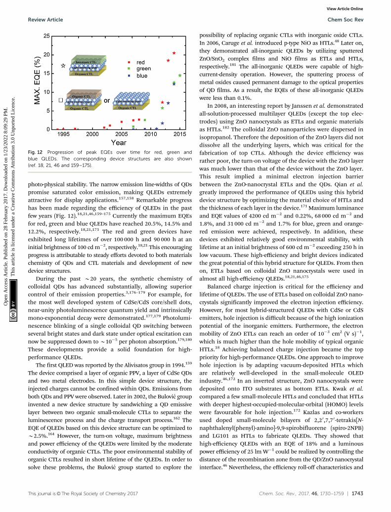
photo-physical stability. The narrow emission line-widths of QDspromise saturated color emission, making QLEDs extremelyattractive for display applications.157,158 Remarkable progresshas been made regarding the efficiency of QLEDs in the pastfew years (Fig. 12).18,21,46,159–175 Currently the maximum EQEsfor red, green and blue QLEDs have reached 20.5%, 14.5% and12.2%, respectively.18,21,175 The red and green devices haveexhibited long lifetimes of over 100 000 h and 90 000 h at aninitial brightness of 100 cd m�2, respectively.18,21 This encouragingprogress is attributable to steady efforts devoted to both materialschemistry of QDs and CTL materials and development of newdevice structures.
During the past B20 years, the synthetic chemistry ofcolloidal QDs has advanced substantially, allowing superiorcontrol of their emission properties.3,176–179 For example, forthe most well developed system of CdSe/CdS core/shell dots,near-unity photoluminescence quantum yield and intrinsicallymono-exponential decay were demonstrated.177,179 Photolumi-nescence blinking of a single colloidal QD switching betweenseveral bright states and dark state under optical excitation cannow be suppressed down to B10�5 per photon absorption.179,180
These developments provide a solid foundation for high-performance QLEDs.
The first QLED was reported by the Alivisatos group in 1994.159
The device comprised a layer of organic PPV, a layer of CdSe QDsand two metal electrodes. In this simple device structure, theinjected charges cannot be confined within QDs. Emissions fromboth QDs and PPV were observed. Later in 2002, the Bulovic groupinvented a new device structure by sandwiching a QD emissivelayer between two organic small-molecule CTLs to separate theluminescence process and the charge transport process.162 TheEQE of QLEDs based on this device structure can be optimized toB2.5%.164 However, the turn-on voltage, maximum brightnessand power efficiency of the QLEDs were limited by the moderateconductivity of organic CTLs. The poor environmental stability oforganic CTLs resulted in short lifetime of the QLEDs. In order tosolve these problems, the Bulovic group started to explore the
possibility of replacing organic CTLs with inorganic oxide CTLs.In 2006, Caruge et al. introduced p-type NiO as HTLs.48 Later on,they demonstrated all-inorganic QLEDs by utilizing sputteredZnO/SnO2 complex films and NiO films as ETLs and HTLs,respectively.181 The all-inorganic QLEDs were capable of high-current-density operation. However, the sputtering process ofmetal oxides caused permanent damage to the optical propertiesof QD films. As a result, the EQEs of these all-inorganic QLEDswere less than 0.1%.
In 2008, an interesting report by Janssen et al. demonstratedall-solution-processed multilayer QLEDs (except the top elec-trodes) using ZnO nanocrystals as ETLs and organic materialsas HTLs.182 The colloidal ZnO nanoparticles were dispersed inisopropanol. Therefore the deposition of the ZnO layers did notdissolve all the underlying layers, which was critical for thefabrication of top CTLs. Although the device efficiency wasrather poor, the turn-on voltage of the device with the ZnO layerwas much lower than that of the device without the ZnO layer.This result implied a minimal electron injection barrierbetween the ZnO-nanocrystal ETLs and the QDs. Qian et al.greatly improved the performance of QLEDs using this hybriddevice structure by optimizing the material choice of HTLs andthe thickness of each layer in the device.171 Maximum luminanceand EQE values of 4200 cd m�2 and 0.22%, 68 000 cd m�2 and1.8%, and 31 000 cd m�2 and 1.7% for blue, green and orange-red emission were achieved, respectively. In addition, thesedevices exhibited relatively good environmental stability, withlifetime at an initial brightness of 600 cd m�2 exceeding 250 h inlow vacuum. These high-efficiency and bright devices indicatedthe great potential of this hybrid structure for QLEDs. From thenon, ETLs based on colloidal ZnO nanocrystals were used inalmost all high-efficiency QLEDs.18,21,46,175
Balanced charge injection is critical for the efficiency andlifetime of QLEDs. The use of ETLs based on colloidal ZnO nano-crystals significantly improved the electron injection efficiency.However, for most hybrid-structured QLEDs with CdSe or CdSemitters, hole injection is difficult because of the high ionizationpotential of the inorganic emitters. Furthermore, the electronmobility of ZnO ETLs can reach an order of 10�3 cm2 (V s)�1,which is much higher than the hole mobility of typical organicHTLs.18 Achieving balanced charge injection became the toppriority for high-performance QLEDs. One approach to improvehole injection is by adapting vacuum-deposited HTLs whichare relatively well-developed in the small-molecule OLEDindustry.46,172 In an inverted structure, ZnO nanocrystals weredeposited onto ITO substrates as bottom ETLs. Kwak et al.compared a few small-molecule HTLs and concluded that HTLswith deeper highest-occupied-molecular-orbital (HOMO) levelswere favourable for hole injection.172 Kazlas and co-workersused doped small-molecule bilayers of 2,20,7,7 0-tetrakis[N-naphthalenyl(phenyl)-amino]-9,9-spirobifluorene (spiro-2NPB)and LG101 as HTLs to fabricate QLEDs. They showed thathigh-efficiency QLEDs with an EQE of 18% and a luminouspower efficiency of 25 lm W�1 could be realized by controlling thedistance of the recombination zone from the QD/ZnO nanocrystalinterface.46 Nevertheless, the efficiency roll-off characteristics and
Fig. 12 Progression of peak EQEs over time for red, green andblue QLEDs. The corresponding device structures are also shown(ref. 18, 21, 46 and 159–175).
Review Article Chem Soc Rev
Ope
n A
cces
s A
rtic
le. P
ublis
hed
on 2
8 Fe
brua
ry 2
017.
Dow
nloa
ded
on 1
/23/
2022
8:0
9:29
PM
. T
his
artic
le is
lice
nsed
und
er a
Cre
ativ
e C
omm
ons
Attr
ibut
ion
3.0
Unp
orte
d L
icen
ce.
View Article Online
1744 | Chem. Soc. Rev., 2017, 46, 1730--1759 This journal is©The Royal Society of Chemistry 2017
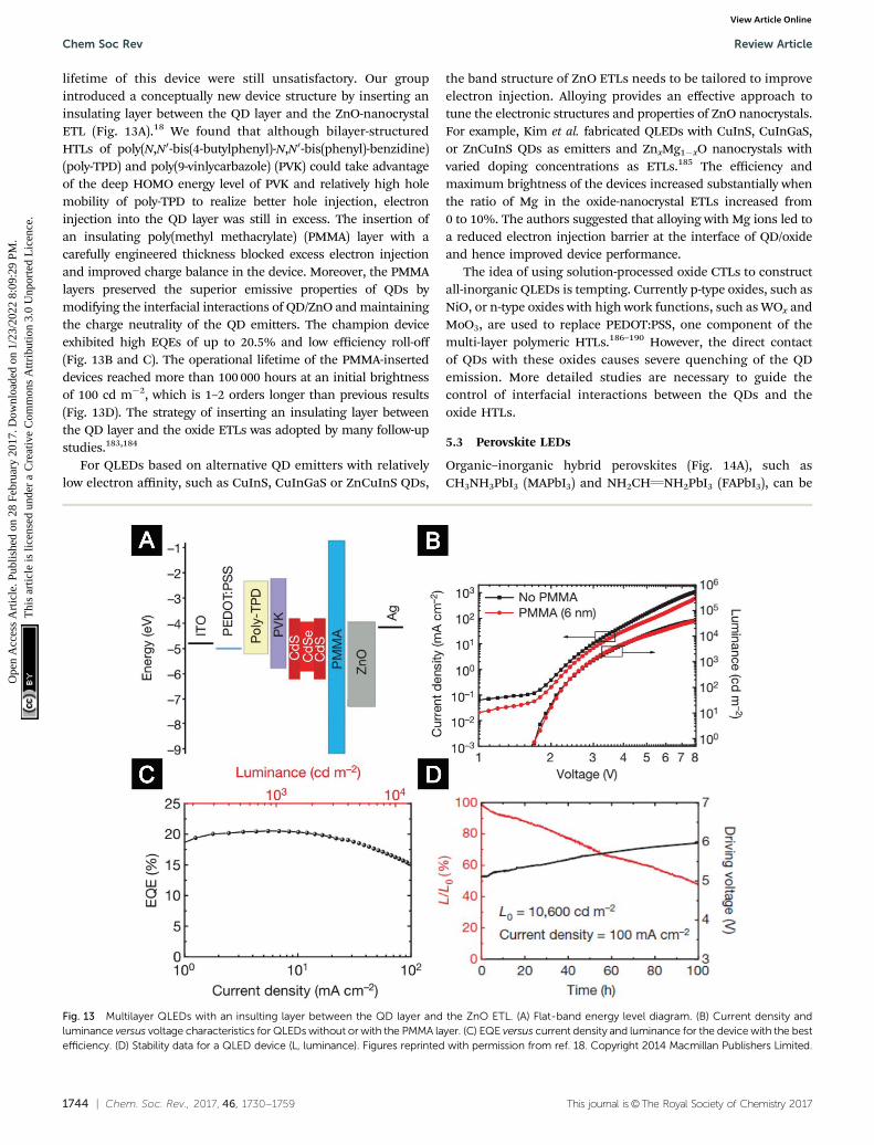
lifetime of this device were still unsatisfactory. Our groupintroduced a conceptually new device structure by inserting aninsulating layer between the QD layer and the ZnO-nanocrystalETL (Fig. 13A).18 We found that although bilayer-structuredHTLs of poly(N,N0-bis(4-butylphenyl)-N,N0-bis(phenyl)-benzidine)(poly-TPD) and poly(9-vinlycarbazole) (PVK) could take advantageof the deep HOMO energy level of PVK and relatively high holemobility of poly-TPD to realize better hole injection, electroninjection into the QD layer was still in excess. The insertion ofan insulating poly(methyl methacrylate) (PMMA) layer with acarefully engineered thickness blocked excess electron injectionand improved charge balance in the device. Moreover, the PMMAlayers preserved the superior emissive properties of QDs bymodifying the interfacial interactions of QD/ZnO and maintainingthe charge neutrality of the QD emitters. The champion deviceexhibited high EQEs of up to 20.5% and low efficiency roll-off(Fig. 13B and C). The operational lifetime of the PMMA-inserteddevices reached more than 100 000 hours at an initial brightnessof 100 cd m�2, which is 1–2 orders longer than previous results(Fig. 13D). The strategy of inserting an insulating layer betweenthe QD layer and the oxide ETLs was adopted by many follow-upstudies.183,184
For QLEDs based on alternative QD emitters with relativelylow electron affinity, such as CuInS, CuInGaS or ZnCuInS QDs,
the band structure of ZnO ETLs needs to be tailored to improveelectron injection. Alloying provides an effective approach totune the electronic structures and properties of ZnO nanocrystals.For example, Kim et al. fabricated QLEDs with CuInS, CuInGaS,or ZnCuInS QDs as emitters and ZnxMg1�xO nanocrystals withvaried doping concentrations as ETLs.185 The efficiency andmaximum brightness of the devices increased substantially whenthe ratio of Mg in the oxide-nanocrystal ETLs increased from0 to 10%. The authors suggested that alloying with Mg ions led toa reduced electron injection barrier at the interface of QD/oxideand hence improved device performance.
The idea of using solution-processed oxide CTLs to constructall-inorganic QLEDs is tempting. Currently p-type oxides, such asNiO, or n-type oxides with high work functions, such as WOx andMoO3, are used to replace PEDOT:PSS, one component of themulti-layer polymeric HTLs.186–190 However, the direct contactof QDs with these oxides causes severe quenching of the QDemission. More detailed studies are necessary to guide thecontrol of interfacial interactions between the QDs and theoxide HTLs.
5.3 Perovskite LEDs
Organic–inorganic hybrid perovskites (Fig. 14A), such asCH3NH3PbI3 (MAPbI3) and NH2CHQNH2PbI3 (FAPbI3), can be
Fig. 13 Multilayer QLEDs with an insulting layer between the QD layer and the ZnO ETL. (A) Flat-band energy level diagram. (B) Current density andluminance versus voltage characteristics for QLEDs without or with the PMMA layer. (C) EQE versus current density and luminance for the device with the bestefficiency. (D) Stability data for a QLED device (L, luminance). Figures reprinted with permission from ref. 18. Copyright 2014 Macmillan Publishers Limited.
Chem Soc Rev Review Article
Ope
n A
cces
s A
rtic
le. P
ublis
hed
on 2
8 Fe
brua
ry 2
017.
Dow
nloa
ded
on 1
/23/
2022
8:0
9:29
PM
. T
his
artic
le is
lice
nsed
und
er a
Cre
ativ
e C
omm
ons
Attr
ibut
ion
3.0
Unp
orte
d L
icen
ce.
View Article Online
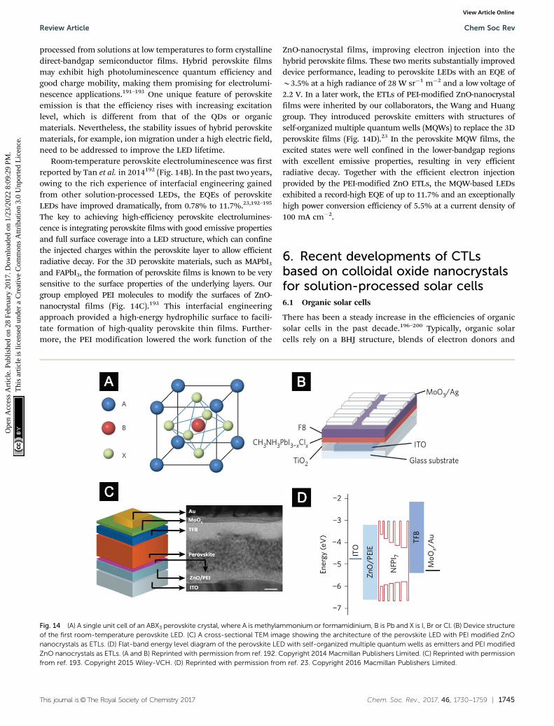
This journal is©The Royal Society of Chemistry 2017 Chem. Soc. Rev., 2017, 46, 1730--1759 | 1745
processed from solutions at low temperatures to form crystallinedirect-bandgap semiconductor films. Hybrid perovskite filmsmay exhibit high photoluminescence quantum efficiency andgood charge mobility, making them promising for electrolumi-nescence applications.191–193 One unique feature of perovskiteemission is that the efficiency rises with increasing excitationlevel, which is different from that of the QDs or organicmaterials. Nevertheless, the stability issues of hybrid perovskitematerials, for example, ion migration under a high electric field,need to be addressed to improve the LED lifetime.
Room-temperature perovskite electroluminescence was firstreported by Tan et al. in 2014192 (Fig. 14B). In the past two years,owing to the rich experience of interfacial engineering gainedfrom other solution-processed LEDs, the EQEs of perovskiteLEDs have improved dramatically, from 0.78% to 11.7%.23,192–195
The key to achieving high-efficiency perovskite electrolumines-cence is integrating perovskite films with good emissive propertiesand full surface coverage into a LED structure, which can confinethe injected charges within the perovskite layer to allow efficientradiative decay. For the 3D perovskite materials, such as MAPbI3
and FAPbI3, the formation of perovskite films is known to be verysensitive to the surface properties of the underlying layers. Ourgroup employed PEI molecules to modify the surfaces of ZnO-nanocrystal films (Fig. 14C).193 This interfacial engineeringapproach provided a high-energy hydrophilic surface to facili-tate formation of high-quality perovskite thin films. Further-more, the PEI modification lowered the work function of the
ZnO-nanocrystal films, improving electron injection into thehybrid perovskite films. These two merits substantially improveddevice performance, leading to perovskite LEDs with an EQE ofB3.5% at a high radiance of 28 W sr�1 m�2 and a low voltage of2.2 V. In a later work, the ETLs of PEI-modified ZnO-nanocrystalfilms were inherited by our collaborators, the Wang and Huanggroup. They introduced perovskite emitters with structures ofself-organized multiple quantum wells (MQWs) to replace the 3Dperovskite films (Fig. 14D).23 In the perovskite MQW films, theexcited states were well confined in the lower-bandgap regionswith excellent emissive properties, resulting in very efficientradiative decay. Together with the efficient electron injectionprovided by the PEI-modified ZnO ETLs, the MQW-based LEDsexhibited a record-high EQE of up to 11.7% and an exceptionallyhigh power conversion efficiency of 5.5% at a current density of100 mA cm�2.
6. Recent developments of CTLsbased on colloidal oxide nanocrystalsfor solution-processed solar cells6.1 Organic solar cells
There has been a steady increase in the efficiencies of organicsolar cells in the past decade.196–200 Typically, organic solarcells rely on a BHJ structure, blends of electron donors and
Fig. 14 (A) A single unit cell of an ABX3 perovskite crystal, where A is methylammonium or formamidinium, B is Pb and X is I, Br or Cl. (B) Device structureof the first room-temperature perovskite LED. (C) A cross-sectional TEM image showing the architecture of the perovskite LED with PEI modified ZnOnanocrystals as ETLs. (D) Flat-band energy level diagram of the perovskite LED with self-organized multiple quantum wells as emitters and PEI modifiedZnO nanocrystals as ETLs. (A and B) Reprinted with permission from ref. 192. Copyright 2014 Macmillan Publishers Limited. (C) Reprinted with permissionfrom ref. 193. Copyright 2015 Wiley-VCH. (D) Reprinted with permission from ref. 23. Copyright 2016 Macmillan Publishers Limited.
Review Article Chem Soc Rev
Ope
n A
cces
s A
rtic
le. P
ublis
hed
on 2
8 Fe
brua
ry 2
017.
Dow
nloa
ded
on 1
/23/
2022
8:0
9:29
PM
. T
his
artic
le is
lice
nsed
und
er a
Cre
ativ
e C
omm
ons
Attr
ibut
ion
3.0
Unp
orte
d L
icen
ce.
View Article Online
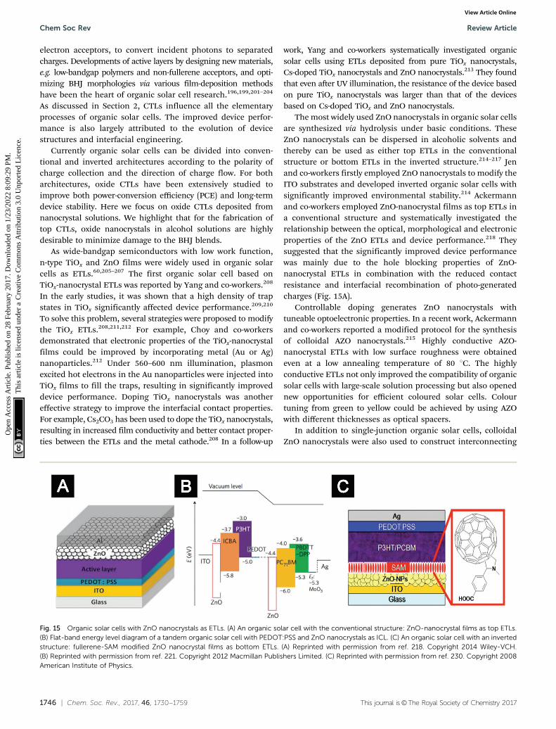
1746 | Chem. Soc. Rev., 2017, 46, 1730--1759 This journal is©The Royal Society of Chemistry 2017
electron acceptors, to convert incident photons to separatedcharges. Developments of active layers by designing new materials,e.g. low-bandgap polymers and non-fullerene acceptors, and opti-mizing BHJ morphologies via various film-deposition methodshave been the heart of organic solar cell research.196,199,201–204
As discussed in Section 2, CTLs influence all the elementaryprocesses of organic solar cells. The improved device perfor-mance is also largely attributed to the evolution of devicestructures and interfacial engineering.
Currently organic solar cells can be divided into conven-tional and inverted architectures according to the polarity ofcharge collection and the direction of charge flow. For botharchitectures, oxide CTLs have been extensively studied toimprove both power-conversion efficiency (PCE) and long-termdevice stability. Here we focus on oxide CTLs deposited fromnanocrystal solutions. We highlight that for the fabrication oftop CTLs, oxide nanocrystals in alcohol solutions are highlydesirable to minimize damage to the BHJ blends.
As wide-bandgap semiconductors with low work function,n-type TiOx and ZnO films were widely used in organic solarcells as ETLs.60,205–207 The first organic solar cell based onTiOx-nanocrystal ETLs was reported by Yang and co-workers.208
In the early studies, it was shown that a high density of trapstates in TiOx significantly affected device performance.209,210
To solve this problem, several strategies were proposed to modifythe TiOx ETLs.208,211,212 For example, Choy and co-workersdemonstrated that electronic properties of the TiOx-nanocrystalfilms could be improved by incorporating metal (Au or Ag)nanoparticles.212 Under 560–600 nm illumination, plasmonexcited hot electrons in the Au nanoparticles were injected intoTiOx films to fill the traps, resulting in significantly improveddevice performance. Doping TiOx nanocrystals was anothereffective strategy to improve the interfacial contact properties.For example, Cs2CO3 has been used to dope the TiOx nanocrystals,resulting in increased film conductivity and better contact proper-ties between the ETLs and the metal cathode.208 In a follow-up
work, Yang and co-workers systematically investigated organicsolar cells using ETLs deposited from pure TiOx nanocrystals,Cs-doped TiOx nanocrystals and ZnO nanocrystals.213 They foundthat even after UV illumination, the resistance of the device basedon pure TiOx nanocrystals was larger than that of the devicesbased on Cs-doped TiOx and ZnO nanocrystals.
The most widely used ZnO nanocrystals in organic solar cellsare synthesized via hydrolysis under basic conditions. TheseZnO nanocrystals can be dispersed in alcoholic solvents andthereby can be used as either top ETLs in the conventionalstructure or bottom ETLs in the inverted structure.214–217 Jenand co-workers firstly employed ZnO nanocrystals to modify theITO substrates and developed inverted organic solar cells withsignificantly improved environmental stability.214 Ackermannand co-workers employed ZnO-nanocrystal films as top ETLs ina conventional structure and systematically investigated therelationship between the optical, morphological and electronicproperties of the ZnO ETLs and device performance.218 Theysuggested that the significantly improved device performancewas mainly due to the hole blocking properties of ZnO-nanocrystal ETLs in combination with the reduced contactresistance and interfacial recombination of photo-generatedcharges (Fig. 15A).
Controllable doping generates ZnO nanocrystals withtuneable optoelectronic properties. In a recent work, Ackermannand co-workers reported a modified protocol for the synthesisof colloidal AZO nanocrystals.215 Highly conductive AZO-nanocrystal ETLs with low surface roughness were obtainedeven at a low annealing temperature of 80 1C. The highlyconductive ETLs not only improved the compatibility of organicsolar cells with large-scale solution processing but also openednew opportunities for efficient coloured solar cells. Colourtuning from green to yellow could be achieved by using AZOwith different thicknesses as optical spacers.
In addition to single-junction organic solar cells, colloidalZnO nanocrystals were also used to construct interconnecting
Fig. 15 Organic solar cells with ZnO nanocrystals as ETLs. (A) An organic solar cell with the conventional structure: ZnO-nanocrystal films as top ETLs.(B) Flat-band energy level diagram of a tandem organic solar cell with PEDOT:PSS and ZnO nanocrystals as ICL. (C) An organic solar cell with an invertedstructure: fullerene-SAM modified ZnO nanocrystal films as bottom ETLs. (A) Reprinted with permission from ref. 218. Copyright 2014 Wiley-VCH.(B) Reprinted with permission from ref. 221. Copyright 2012 Macmillan Publishers Limited. (C) Reprinted with permission from ref. 230. Copyright 2008American Institute of Physics.
Chem Soc Rev Review Article
Ope
n A
cces
s A
rtic
le. P
ublis
hed
on 2
8 Fe
brua
ry 2
017.
Dow
nloa
ded
on 1
/23/
2022
8:0
9:29
PM
. T
his
artic
le is
lice
nsed
und
er a
Cre
ativ
e C
omm
ons
Attr
ibut
ion
3.0
Unp
orte
d L
icen
ce.
View Article Online
This journal is©The Royal Society of Chemistry 2017 Chem. Soc. Rev., 2017, 46, 1730--1759 | 1747
layers (ICLs) and minimize loss of open-circuit voltage (VOC) intandem solar cells.55,219–221 ICLs are sandwiched by two organicsolar cell stacks and act as the charge recombination zone. ICLsgenerally consist of a p-type HTL and an n-type ETL, servingto shift vacuum level via alignment of the Fermi levels.205,222
ZnO-nanocrystal layers with high conductivity can be obtainedby low-temperature deposition procedures, which is desirableto minimize morphological changes of active layers used inbottom cells. By employing ZnO nanocrystal/PEDOT:PSS as theICLs, Yang and co-workers demonstrated two-junction tandemsolar cells with high PCEs of 8.6% and 10.6% (Fig. 15B).219,221
In this tandem device, the VOC was close to the sum of VOC
of two single junction cells with a negligible loss of B0.03 V.ICLs based on ZnO nanocrystals were also efficient for triple-junction tandem solar cells. By inserting two ICLs comprisingZnO nanocrystals, triple-junction polymer solar cells with a PCEof over 11% were fabricated.223 Moreover, ZnO nanocrystals canform ideal ICLs not only with PEDOT:PSS but also with othermaterials, e.g. conjugated polyelectrolyte layers. Heeger andco-workers demonstrated a tandem device with a PCE of 8.6%based on the ZnO nanocrystals/conjugated polyelectrolyteICLs.224 Recently, a higher PCE of 11.3% was achieved byincorporating highly self-doped conjugated polyelectrolytesand ZnO nanocrystals as the ICLs.225
Despite the success of applying colloidal ZnO nanocrystalsin single-junction and tandem organic solar cells, a majorchallenge lies in how to control intragap states induced bysurface defects. It has been reported that surface defects ofZnO nanocrystals caused significant photocurrent loss anddegraded charge selectivity of the cathode interface.226,227 Prosaet al. showed that the release of oxygen chemisorbed ontothe surfaces of ZnO nanocrystals under UV irradiation causedphoto-induced shunts, resulting in reduced charge selectivityat the cathode interface.228 This process represents an issue forthe long-term photo-stability of organic solar cells. Riedl andco-workers showed that photo-induced shunting is a generalphenomenon in neat and doped ZnO-based ETLs regardlessof whether they are deposited from nanoparticle solutions orby vacuum deposition.229 Several strategies to passivate thesurface defects of ZnO-nanocrystal ETLs have been proposed.For example, Jen and co-workers introduced fullerene-basedSAMs to avoid direct contact of ZnO nanocrystals with activelayers (Fig. 15C).230 Coordination polymers such as poly(ethyleneoxide) (PEO) and poly(ethylene glycol) (PEG) were also usedto passivate surface defects of ZnO nanocrystals, leading toimproved device performance.231–233 So and co-workers showedthat UV-ozone treatment efficiently passivated the defect statesof ZnO nanocrystals, as indicated by the suppression of defectemission in the photoluminescence measurements.227 In arecent work, we developed a facial EDT treatment to modulatethe intragap states of ZnO-nanocrystal films. The covalentbonding of EDT molecules onto ZnO nanocrystals removed alarge fraction of the surface defects and introduced a newintragap band, resulting in enhanced electron transport andminimized interfacial bimolecular recombination loss of theresulting solar cells.19 In addition, the well-passivated ZnO
nanocrystals were less susceptible to oxygen and water moleculesand hence further improved the ambient stability of obtaineddevices.
HTLs based on high work-function and n-type oxide nano-crystals, such as MoOx and WOx, have also been explored fororganic solar cells.156,234–236 For example, Lee et al. developeda facile approach to synthesize MoOx nanocrystals based on amicrowave-assisted method.234 The devices with MoOx-nanocrystalHTLs exhibited PCEs comparable to those of devices withPEDOT:PSS HTLs. In a recent report, low-temperature solution-processed WO3 nanocrystals were employed as HTLs in organicsolar cells by Brabec and co-workers.235 The small WO3 nano-crystals were stabilized in alcohol-based solvents. SmoothWO3-nanocrystal films were obtained after a mild thermalannealing process (80 1C for 5 min), making them compatiblewith conventional and inverted organic solar cells. HTLs basedon V2O5 nanocrystals and mixed-oxide nanocrystals of WO3
and V2O5 have also been introduced to improve the deviceperformance.236 It was shown that the mixed oxide nanocrystalscould effectively suppress the leakage current and enhanceoptical absorption, resulting in more efficient and stable devices.
Solution-processed p-type NiOx films with high work functioncan function as hole transporting and electron blocking layerssimultaneously in organic solar cells.237,238 Recently, we appliedpure NiO nanocrystals synthesized by the ligand-protectionstrategy to the fabrication of HTLs.25 UV-ozone treatment wasused to remove the insulating surface ligands and increasethe work function of NiO films (Fig. 16A–D). The devices withNiO-nanocrystal HTLs exhibited an average PCE of 6.1%.In contrast, the average PCE for the devices with PEDOT:PSSas HTLs was 5.0%. In a recent report, Choy and co-workersreported a novel approach for the synthesis of nonstoichio-metric NiOx nanocrystals.24 After carefully controlled calcination(270 1C for 2 h) in air, the obtained dark-black NiOx nanocrystalswere well dispersed in water to form a stable solution. Evenwithout any post-deposition treatment, the HTLs based on NiOx
nanocrystals offered a high work function of 5.25 eV, providingexcellent contact for most donor materials in organic solar cells(Fig. 16E and F).
6.2 QDSCs
Colloidal QDs are attractive for solar cells because of theunique combination of solution-processable characteristics,size-dependent electronic structure, excellent absorption inthe visible and infrared region, and potential multi-excitongeneration.239–242 In the early stages, QDSCs adopted theSchottky structure, in which QDs were sandwiched betweenITO and a low-work-function metal, such as Al and Mg.243–246
However, the Schottky-structured devices suffered from lowVOC due to Fermi-level pinning at the Schottky interfaces,as well as inefficient carrier collection because most of thephoto-excitations occurred at the regions away from the junctionside. The evolution of a Schottky structure to a depleted-heterojunction device with n-type metal oxides as ETLs effec-tively increased the built-in electric field, giving rise to muchimproved device performance.239,247 In recent years, the PCEs
Review Article Chem Soc Rev
Ope
n A
cces
s A
rtic
le. P
ublis
hed
on 2
8 Fe
brua
ry 2
017.
Dow
nloa
ded
on 1
/23/
2022
8:0
9:29
PM
. T
his
artic
le is
lice
nsed
und
er a
Cre
ativ
e C
omm
ons
Attr
ibut
ion
3.0
Unp
orte
d L
icen
ce.
View Article Online

1748 | Chem. Soc. Rev., 2017, 46, 1730--1759 This journal is©The Royal Society of Chemistry 2017
of QDSCs have shown steady improvements (Fig. 17A), owing toboth surface engineering of QDs and optimization of oxideETLs.22,241,245,247–254 The structure of the device with the high-est certified PCE of 10.6% is shown in Fig. 17B. For this device,ZnO-nanocrystal films were used as ETLs.22
The compositions and surface coordination states of QDs,which heavily rely on the synthesis, purification and processingprocedures, have significant impacts on carrier mobility, defectdensity, as well as doping density of the QD films. Exquisitemodulations of synthetic and purification procedures areimportant for improving the performance of QDSCs.254–256
Ligand engineering of QDs can effectively reduce defect densityand suppress carrier recombination in the QD films, as well astune the absolute energy levels. For example, halide ligandswere explored for passivation of surface defects, leading to QDfilms with higher carrier mobility and thereby much improveddevice performance.250 The Bawendi group showed that theligand-induced surface dipoles could influence the absoluteenergy levels of QD films.117,251 This finding made it appealingto tailor the band energy alignment of the QD layers withcarefully engineered ligands.
For heterojunction QDSCs, the n-type oxide layer is criticalto determine the thickness of the depletion region in the QDlayer, the built-in voltage, as well as electron extraction andtransport. In the early stages, TiO2 paste composed of nano-crystals with sizes of B20 nm and carrier density of B1016 cm�3
was utilized for ETL fabrication.241 A PCE of over 5% wasachieved. Both the VOC and the short-circuit current ( JSC) wereenhanced compared to the device with Schottky structure. Forthe heterojunction QDSCs, the energy level offset between theconduction band of TiO2 and QDs should be favourable tofacilitate electron extraction from QDs to TiO2 while avoidingexcess loss of VOC. For example, the Sargent group studied QDSCsusing two types of TiO2 ETLs, one made from nanocrystals withan electron affinity of �3.8 eV and another one deposited bysputtering with an electron affinity of �4.0 eV.257 The parametersof QDSCs based on nanocrystals and sputtered TiO2 thin filmwere 0.7 and 0.61 V for VOC, 3.5% and 2.7% for PCE, respectively.
Fig. 16 P-type NiOx nanocrystals and their application as HTLs in organic solar cells. (A) A typical TEM image of the colloidal NiO nanocrystalssynthesized by the ligand-protecting method. (B) UPS spectrum of the NiO-nanocrystal HTL. (C) Device structure of organic solar cells with NiO-nanocrystal HTLs and (D) the corresponding J–V curves of the devices. (E) A typical TEM image of the NiOx nanoparticles synthesized by the chemicalprecipitation method and (F) energy-level diagram of the NiOx-nanocrystal HTL without any post-deposition treatment. (A–D) Reprinted with permissionfrom ref. 25. Copyright 2014 American Chemical Society. (E–F) Reprinted with permission from ref. 24. Copyright 2015 Wiley-VCH.
Fig. 17 (A) Progression of the PCE of QDSCs over time (ref. 22, 245and 247–252). The PCEs of QDSCs with depleted-heterojunction struc-tures are certified values. (B) Device architecture of the QDSC achievingthe highest certified PCE to date. (B) Adapted with permission from ref. 22.Copyright 2016 American Chemical Society.
Chem Soc Rev Review Article
Ope
n A
cces
s A
rtic
le. P
ublis
hed
on 2
8 Fe
brua
ry 2
017.
Dow
nloa
ded
on 1
/23/
2022
8:0
9:29
PM
. T
his
artic
le is
lice
nsed
und
er a
Cre
ativ
e C
omm
ons
Attr
ibut
ion
3.0
Unp
orte
d L
icen
ce.
View Article Online
This journal is©The Royal Society of Chemistry 2017 Chem. Soc. Rev., 2017, 46, 1730--1759 | 1749
Given that the electron affinity of QDs used in the devices isB3.6 eV, the authors suggested that the energy-level offset of0.2 eV favoured electron injection from QDs to TiO2 nanocrystalthin films.257 For the sputtered TiO2 thin film, the deeper TiO2
band-edge compromised the VOC.Interfacial recombination is an important loss pathway that
may limit JSC and degrade device efficiency.258 Sargent andco-workers showed that inserting a buffer layer of ZnO onto thesurface of TiO2 effectively reduced interfacial recombination,leading to remarkably improved device performance.255 Thiswork suggests that defect centers in TiO2 are one limitingfactor for device performance. This work also implies that ZnOmay outperform TiO2 in terms of suppressing interfacialrecombination.
Currently the majority of the state-of-the-art high-efficiencyQDSCs use solution-processed ZnO, e.g. ZnO-nanocrystalfilms, as ETLs.20,22 The relationship between the properties ofZnO-nanocrystal ETLs and device performance has been inves-tigated by a number of studies. For example, in a QDSC with aninverted structure, effects of varying the doping density of theZnO-nanocrystal films by illumination were explored.256 UnderUV illumination, the absorbed gas molecules, for example O2,on the surfaces of ZnO nanocrystals were removed, resulting inenhanced doping density. Consequently, an additional portionof the depletion region was formed within the hole acceptingPbS layer. These effects led to a transition from excitonicbehavior to p–n behavior in the device, leading to enhancedcharge generation and extraction. In another work, Azmi andco-workers applied the EDT surface passivation method developedby our group to the ZnO-nanocrystal ETLs used in QDSCs.259 Theyconfirmed that the intragap trap states originating from thenotorious oxygen-deficient surface states of the ZnO nanocrystalswere effectively removed after the EDT treatment. This treatmentsuppressed interfacial charge recombination at the QD/ETLheterojunction and the PCE was improved from 9.45 to10.26%. Very recently, Kim et al. showed that addition oforganic molecules with strong dipole moment decreased thework function of the ZnO layer, giving rise to increased built-involtage and better device performance.20 As a result, a remarkablePCE of 10.7% was obtained.
6.3 Perovskite solar cells
Metal halide perovskite solar cells have attracted worldwideattention in recent years due to their high efficiencies and lowprocessing cost.260–266 Owing to the rapid developments ofperovskite materials, film deposition and processing and inter-facial engineering, the efficiencies of perovskite solar cells haverocketed from the first reported 3.8% to a certified 22.1% overthe past few years. Some recent works, such as using cesiumions along with formamidinium cations in lead bromide–iodidecells and two-dimensional Ruddlesden–Popper perovskite solarcells, have shed light on addressing critical factors of thermal- andphoto-stability under operating conditions.267,268
Initial studies of perovskite solar cells focused on a devicestructure similar to dye-sensitized solar cells with meso-porous TiO2 or Al2O3 as the scaffolds.6,269 High temperature
(450–500 1C) sintered compact TiO2 layers were often used.Further investigation revealed that perovskite materials exhibitedambipolar charge transport and long charge diffusion length,resulting in the success of perovskite solar cells with simplifiedplanar heterojunction (PHJ) structures, in which the perovskitelayer was sandwiched between ETL and HTL.270–273 Various CTLsdeveloped for other solution-processed optoelectronics weredemonstrated to be suitable for perovskite solar cells. Amongthem, CTLs based on colloidal oxide nanocrystals showed greatpotential. Depending on selective charge extraction and trans-port properties of the bottom contacts, the PHJ solar cells canbe further divided into two sub-categories, conventional (n–i–p)and inverted (p–i–n) structure.274 In this section, we will discussa few relevant examples.
The first PHJ perovskite solar cell developed by Snaith andco-workers was based on high-temperature-sintered compactTiO2 ETLs by gradually decreasing the thickness of Al2O3
scaffolds used in mesoporous devices.6 By employing high-conductivity yttrium-doped TiO2 nanocrystals as ETLs, Yangand co-workers demonstrated one of the most efficient planardevices based on TiO2 ETLs.263 The yttrium doping increasedthe conductivity of TiO2-nanocrystal films from 6 � 10�6 to2 � 10�5 S cm�1 and significantly improved charge transportin the devices. By further reducing the work function of ITOsubstrates with PEIE and controlling the humidity of theannealing atmosphere, planar devices with the best PCE of19.3% and an average PCE of 16.6% were obtained. In additionto TiO2 nanocrystals, ZnO nanocrystals were also employed asETLs in conventional planar perovskite solar cells. Liu et al. firstintroduced ZnO nanocrystals as the ETLs for the fabrication ofefficient perovskite solar cells at low temperatures (Fig. 18A).275
Highly conductive crystalline SnO2 and Zn2SnO4 (ZSO) nano-crystals were also used as efficient ETLs in conventional PHJperovskite solar cells.276,277 For example, Rao et al. employedSnO2 nano-colloids to deposit ETLs for PHJ perovskite solarcells.278 Compared to the TiO2, the SnO2 ETLs exhibited highermobility, resulting in improved photocurrent and device perfor-mance. Recently, Seok and co-workers fabricated PHJ perovskitesolar cells by employing ETLs deposited from highly dispersedZSO nanocrystal solutions.277,279 A relatively low temperature(100 1C) was sufficient to obtain ZSO-nanocrystal films with highelectron mobility. Moreover, due to its low refractive index, theinsertion of the ZSO layer further improved the transmittance ofsubstrates in the visible regions. Based on the high-quality ZSOETLs, flexible perovskite solar cells with a PCE of B15% wereachieved.277 By further tailoring the energy level and electrontransporting properties of ZSO ETLs using nanocrystals withdifferent sizes, the loss of photogenerated electrons was furtherreduced. An improved PCE of B16% was achieved for thedevices based on flexible substrates.279
Currently a critical issue at the interfaces of oxide/perovskiteis the lack of control over the sensitive surface states of theoxide nanocrystals. For example, it was shown that oxygenvacancy due to the light-induced desorption of surfaceabsorbed oxygen in TiOx films accounted for poor stability ofTiO2-based devices.280 For devices based on ZnO ETLs, surface
Review Article Chem Soc Rev
Ope
n A
cces
s A
rtic
le. P
ublis
hed
on 2
8 Fe
brua
ry 2
017.
Dow
nloa
ded
on 1
/23/
2022
8:0
9:29
PM
. T
his
artic
le is
lice
nsed
und
er a
Cre
ativ
e C
omm
ons
Attr
ibut
ion
3.0
Unp
orte
d L
icen
ce.
View Article Online
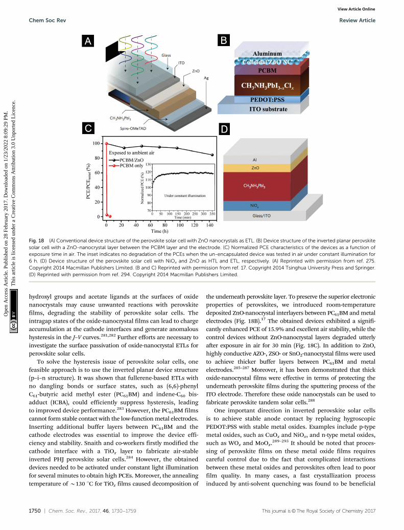
1750 | Chem. Soc. Rev., 2017, 46, 1730--1759 This journal is©The Royal Society of Chemistry 2017
hydroxyl groups and acetate ligands at the surfaces of oxidenanocrystals may cause unwanted reactions with perovskitefilms, degrading the stability of perovskite solar cells. Theintragap states of the oxide-nanocrystal films can lead to chargeaccumulation at the cathode interfaces and generate anomaloushysteresis in the J–V curves.281,282 Further efforts are necessary toinvestigate the surface passivation of oxide-nanocrystal ETLs forperovskite solar cells.
To solve the hysteresis issue of perovskite solar cells, onefeasible approach is to use the inverted planar device structure(p–i–n structure). It was shown that fullerene-based ETLs withno dangling bonds or surface states, such as (6,6)-phenylC61-butyric acid methyl ester (PC61BM) and indene-C60 bis-adduct (ICBA), could efficiently suppress hysteresis, leadingto improved device performance.283 However, the PC61BM filmscannot form stable contact with the low-function metal electrodes.Inserting additional buffer layers between PC61BM and thecathode electrodes was essential to improve the device effi-ciency and stability. Snaith and co-workers firstly modified thecathode interface with a TiOx layer to fabricate air-stableinverted PHJ perovskite solar cells.284 However, the obtaineddevices needed to be activated under constant light illuminationfor several minutes to obtain high PCEs. Moreover, the annealingtemperature of B130 1C for TiOx films caused decomposition of
the underneath perovskite layer. To preserve the superior electronicproperties of perovskites, we introduced room-temperaturedeposited ZnO-nanocrystal interlayers between PC61BM and metalelectrodes (Fig. 18B).17 The obtained devices exhibited a signifi-cantly enhanced PCE of 15.9% and excellent air stability, while thecontrol devices without ZnO-nanocrystal layers degraded utterlyafter exposure in air for 30 min (Fig. 18C). In addition to ZnO,highly conductive AZO-, ZSO- or SnO2-nanocrystal films were usedto achieve thicker buffer layers between PC61BM and metalelectrodes.285–287 Moreover, it has been demonstrated that thickoxide-nanocrystal films were effective in terms of protecting theunderneath perovskite films during the sputtering process of theITO electrode. Therefore these oxide nanocrystals can be used tofabricate perovskite tandem solar cells.288
One important direction in inverted perovskite solar cellsis to achieve stable anode contact by replacing hygroscopicPEDOT:PSS with stable metal oxides. Examples include p-typemetal oxides, such as CuOx and NiOx, and n-type metal oxides,such as WOx and MoOx.289–293 It should be noted that proces-sing of perovskite films on these metal oxide films requirescareful control due to the fact that complicated interactionsbetween these metal oxides and perovskites often lead to poorfilm quality. In many cases, a fast crystallization processinduced by anti-solvent quenching was found to be beneficial
Fig. 18 (A) Conventional device structure of the perovskite solar cell with ZnO nanocrystals as ETL. (B) Device structure of the inverted planar perovskitesolar cell with a ZnO-nanocrystal layer between the PCBM layer and the electrode. (C) Normalized PCE characteristics of the devices as a function ofexposure time in air. The inset indicates no degradation of the PCEs when the un-encapsulated device was tested in air under constant illumination for6 h. (D) Device structure of the perovskite solar cell with NiOx and ZnO as HTL and ETL, respectively. (A) Reprinted with permission from ref. 275.Copyright 2014 Macmillan Publishers Limited. (B and C) Reprinted with permission from ref. 17. Copyright 2014 Tsinghua University Press and Springer.(D) Reprinted with permission from ref. 294. Copyright 2014 Macmillan Publishers Limited.
Chem Soc Rev Review Article
Ope
n A
cces
s A
rtic
le. P
ublis
hed
on 2
8 Fe
brua
ry 2
017.
Dow
nloa
ded
on 1
/23/
2022
8:0
9:29
PM
. T
his
artic
le is
lice
nsed
und
er a
Cre
ativ
e C
omm
ons
Attr
ibut
ion
3.0
Unp
orte
d L
icen
ce.
View Article Online

This journal is©The Royal Society of Chemistry 2017 Chem. Soc. Rev., 2017, 46, 1730--1759 | 1751
in terms of obtaining high-quality perovskite films. Up to now,NiOx is the most widely investigated HTL in inverted perovskitesolar cells. In a recent work by You et al., inverted PHJperovskite solar cells with NiO HTLs and ZnO-nanocrystal ETLswere fabricated (Fig. 18D).294 These devices showed signifi-cantly improved stability against water and oxygen degradation,i.e. less than 10% degradation even after 6 days storage in airwithout encapsulation. NiO HTLs can also be deposited fromnanocrystal solutions.295,296 The devices based on NiO-nanocrystal HTLs exhibited high reproducibility with the bestPCE of 17.6% and an average efficiency of 15.8%. The lowprocessing temperature of the NiO-nanocrystal HTLs enabledthe fabrication of flexible perovskite solar cells with a promis-ing PCE of 14.5%.
7. Conclusions and prospects
Colloidal oxide nanocrystals offer a unique combination ofexcellent low-temperature solution processability, rich and con-trollable optoelectronic properties and intrinsic stability, whichspurred their applications as CTLs for solution-processed solarcells and LEDs (Fig. 19). Fully exploiting the potential of CTLsbased on oxide nanocrystals relies on both in-depth understandingof how the properties of CTLs impact device operation, someof which is currently unknown, to guide material design andon-demand development of material chemistry for colloidaloxide nanocrystals, some of which is currently unavailable, toallow processing of CTLs with desirable properties. The followingaspects shall be paid more attention to in future research.
(i) Ligand chemistry of colloidal oxide nanocrystals. Knowledgeof the ligand chemistry of colloidal oxide nanocrystals is surpris-ingly scarce despite the fact that surface tuning and modificationare imperative for their CTL applications. As-synthesized oxidenanocrystals are often ill-suited for CTL applications. For example,
weak-binding ligands used to stabilize oxide nanocrystals insolutions tend to dissociate from the nanocrystal surfaces duringfilm processing and device operation, leaving unpassivated surfaces.The high-reactivity surfaces of oxide nanocrystals make theproperties of CTLs very sensitive to environments, processingand operational history, which may deteriorate device stability.
We suggest that ligands with strong anchoring groups tofacilitate their tight binding onto surfaces of oxide nanocrystalsshall be used to lower surface activity and improve stability ofthe CTL films. The concept of entropy ligand is likely to be a keyguideline to meet the demands of both stability of colloidaloxide nanocrystals in solution and charge transport of theircorresponding CTLs. It is also possible to further modify theproperties of oxide-nanocrystal CTLs by judicious moleculardesign of functional ligands.
Currently, establishing a link between surface structure ofoxide nanocrystals and electronic/transport properties of thecorresponding CTLs remains a crucial open question in thisfield. We highlight that investigations on ligand chemistrymay provide unique opportunities to achieve complete surfacepassivation of the oxide nanocrystals, providing powerful toolsto understand and manipulate the intragap states of thecorresponding oxide CTLs. Techniques that have been successfulin characterizing the intragap states of other semiconductors,such as thermal admittance spectroscopy, deep-level transientspectroscopy, drive-level capacitance profiling and photo-thermal deflection spectroscopy, may be useful in quantifyingthe intragap states of the oxide-nanocrystal CTLs.
(ii) Synthetic chemistry of p-type oxide nanocrystals. Up tonow, the synthesis of NiO nanocrystals is one of the fewexamples for p-type oxide nanocrystals applicable as HTLs.Synthetic chemistry of NiO nanocrystals is not as mature asthat of n-type oxide nanocrystals. Our studies indicated that theextinction coefficient of NiO-nanocrystal films was about oneorder of magnitude larger than that of other oxide-nanocrystal
Fig. 19 Relationship between the chemistry of colloidal oxide nanocrystals, processing and properties of CTLs and device performance of solution-processed LEDs and solar cells.
Review Article Chem Soc Rev
Ope
n A
cces
s A
rtic
le. P
ublis
hed
on 2
8 Fe
brua
ry 2
017.
Dow
nloa
ded
on 1
/23/
2022
8:0
9:29
PM
. T
his
artic
le is
lice
nsed
und
er a
Cre
ativ
e C
omm
ons
Attr
ibut
ion
3.0
Unp
orte
d L
icen
ce.
View Article Online
1752 | Chem. Soc. Rev., 2017, 46, 1730--1759 This journal is©The Royal Society of Chemistry 2017
CTLs, such as ZnO-nanocrystal films, which may causeunneglectable absorption of photons. More exquisite controlover the band structure, carrier density, intragap states, stoi-chiometry and optical properties of the NiO-nanocrystal HTLsshall be pursued in the future. It is also of interest to developthe synthetic chemistry of other p-type oxide nanocrystals, suchas the ternary Cu(I) delafossite oxides.
(iii) In-depth understanding of interactions between oxide-nanocrystal CTLs and active layers. Detailed mechanistic studieson interactions between oxide-nanocrystal CTLs and active layersunder operational conditions are lacking despite the extensivepractice of applying oxide nanocrystals as CTLs in solution-processed LEDs and solar cells. For example, quenching ofexcitons formed in the QDs by the adjacent oxide CTLs has beenidentified as one critical factor that limits device performance.However, quenching mechanisms under operational conditionshave not been fully disclosed. In our laboratory, preliminarystudies on the photoluminescence of QDs in contact with oxide-nanocrystal films showed that several quenching mechanisms,including photo-induced charge separation and charging ofQDs due to interfacial charge transfer and energy transfer, wereinvolved depending on the properties of both CTLs and QDs.Moreover, electric field and electric current should be takeninto consideration when interpreting the quenching mechanismunder electrically driven conditions. For instance, the electricfield in the QD layer can modify the radiative recombinationrate through spatial separation of the electron and the hole.Multiple techniques, including single-dot photoluminescence orelectroluminescence spectroscopy, electrostatic force microscopy,transient-absorption spectroscopy and in situ photoluminescence–electroluminescence spectroscopy, should be combined to gainmore comprehensive and rigorous understanding and to provideguidelines to exquisite design of oxide-nanocrystal CTLs beyondthe state-of-the-art.
In summary, there is still plenty of room to boost deviceperformance by developing new material chemistry of colloidaloxide nanocrystals and custom-tailoring the properties andprocessing of CTLs. These efforts shall lead to a new generationof high-performance and all-solution-processed solar cells andLEDs with both ETLs and HTLs based on colloidal oxidenanocrystals, which may revolutionize the current LED andsolar-cell industry based on vacuum-deposited crystalline semi-conductors. Furthermore, such knowledge can be transferred tothe research of other solution-processed devices, such as contactengineering of solution-processed field-effect transistors.
Acknowledgements
This work was financially supported by the National KeyResearch and Development Program of China (2016YFB0401602and 2016YFA0204000), the National Natural Science Foundationof China (51522209, 91433204, U1632118, and 21571129),the Fundamental Research Funds for the Central Universities(2015FZA3005), Shanghai Key Research program (16JC1402100),Shanghai International Cooperation Project (16520720700) and
the Carl Tryggers Stiftelse and the Swedish Government StrategicResearch Area in Materials Science on Functional Materials atLinkoping University (Faculty Grant SFO-Mat-LiU # 2009-00971).S. B. is a VINNMER Fellow and Marie Skłodowska-Curie Fellow.We thank Prof. Jianpu Wang (Nanjing Tech University, China),Mr Zhenxing Zhang (Department of Chemistry, Zhejiang Univer-sity, China), Mr Desui Chen (Department of Chemistry, ZhejiangUniversity, China), Mr Yunzhou Deng (Department of Chemistry,Zhejiang University, China), Mr Yang Liu (School of MaterialsScience and Engineering, Zhejiang University, China) and Mr FeiWang (School of Physic Science and Technology, Shanghai TechUniversity, China) for the assistance in preparing this manuscript.
References
1 J. H. Burroughes, A. R. Brown and R. N. Marks, Nature,1990, 347, 539–541.
2 R. H. Friend, R. W. Gymer, A. B. Holmes, J. H. Burroughes,R. N. Marks, C. Taliani, D. D. C. Bradley, D. A. Dos Santos,J. L. Bredas, M. Logdlund and W. R. Salaneck, Nature,1999, 397, 121–128.
3 D. J. Noms, C. B. Murray and M. G. Bawendi, J. Am. Chem.Soc., 1993, 115, 8706.
4 Y. D. Yin and A. P. Alivisatos, Nature, 2005, 437, 664–670.5 X. G. Peng, Nano Res., 2009, 2, 425–447.6 M. M. Lee, J. Teuscher, T. Miyasaka, T. N. Murakami and
H. J. Snaith, Science, 2012, 338, 643–647.7 H. S. Kim, C. R. Lee, J. H. Im, K. B. Lee, T. Moehl,
A. Marchioro, S. J. Moon, R. Humphry-Baker, J. H. Yum,J. E. Moser, M. Gratzel and N. G. Park, Sci. Rep., 2012,2, 591.
8 M. Singh, H. M. Haverinen, P. Dhagat and G. E. Jabbour,Adv. Mater., 2010, 22, 673–685.
9 B. J. de Gans, P. C. Duineveld and U. S. Schubert, Adv.Mater., 2004, 16, 203–213.
10 K. Hwang, Y. S. Jung, Y. J. Heo, F. H. Scholes, S. E. Watkins,J. Subbiah, D. J. Jones, D. Y. Kim and D. Vak, Adv. Mater.,2015, 27, 1241–1247.
11 C. W. Sele, T. von Werne, R. H. Friend and H. Sirringhaus,Adv. Mater., 2005, 17, 997–1001.
12 H. Sirringhaus, T. Kawase, R. H. Friend, T. Shimoda,M. Inbasekaran, W. Wu and E. P. Woo, Science, 2000,290, 2123.
13 B. H. Kim, M. S. Onses, J. B. Lim, S. Nam, N. Oh, H. Kim,K. J. Yu, J. W. Lee, J. H. Kim, S. K. Kang, C. H. Lee, J. Lee,J. H. Shin, N. H. Kim, C. Leal, M. Shim and J. A. Rogers,Nano Lett., 2015, 15, 969–973.
14 V. Wood, M. J. Panzer, J. Chen, M. S. Bradley, J. E. Halpert,M. G. Bawendi and V. Bulovic, Adv. Mater., 2009, 21,2151–2155.
15 J. H. Kim, S. T. Williams, N. Cho, C.-C. Chueh andA. K. Y. Jen, Adv. Energy Mater., 2015, 5, 1401229.
16 H. Zheng, Y. N. Zheng, N. L. Liu, N. Ai, Q. Wang, S. Wu,J. H. Zhou, D. G. Hu, S. F. Yu, S. H. Han, W. Xu, C. Luo,Y. H. Meng, Z. X. Jiong, Y. W. Chen, D. Y. Li, F. Huang,
Chem Soc Rev Review Article
Ope
n A
cces
s A
rtic
le. P
ublis
hed
on 2
8 Fe
brua
ry 2
017.
Dow
nloa
ded
on 1
/23/
2022
8:0
9:29
PM
. T
his
artic
le is
lice
nsed
und
er a
Cre
ativ
e C
omm
ons
Attr
ibut
ion
3.0
Unp
orte
d L
icen
ce.
View Article Online

This journal is©The Royal Society of Chemistry 2017 Chem. Soc. Rev., 2017, 46, 1730--1759 | 1753
J. Wang, J. B. Peng and Y. Cao, Nat. Commun., 2013, 4,2885.
17 S. Bai, Z. W. Wu, X. J. Wu, Y. Z. Jin, N. Zhao, Z. H. Chen,Q. Q. Mei, X. Wang, Z. Z. Ye, T. Song, R. Y. Liu, S.-t. Lee andB. Q. Sun, Nano Res., 2014, 7, 1749–1758.
18 X. L. Dai, Z. X. Zhang, Y. Z. Jin, Y. Niu, H. J. Cao,X. Y. Liang, L. W. Chen, J. P. Wang and X. G. Peng, Nature,2014, 515, 96–99.
19 S. Bai, Y. Z. Jin, X. Y. Liang, Z. Z. Ye, Z. W. Wu, B. Q. Sun,Z. F. Ma, Z. Tang, J. P. Wang, U. Wurfel, F. Gao andF. L. Zhang, Adv. Energy Mater., 2015, 5, 201401606.
20 G. H. Kim, F. P. Garcia de Arquer, Y. J. Yoon, X. Lan,M. X. Liu, O. Voznyy, Z. Y. Yang, F. J. Fan, A. H. Ip,P. Kanjanaboos, S. Hoogland, J. Y. Kim and E. H.Sargent, Nano Lett., 2015, 15, 7691–7696.
21 Y. X. Yang, Y. Zheng, W. R. Cao, A. Titov, J. Hyvonen,J. R. Manders, J. G. Xue, P. H. Holloway and L. Qian,Nat. Photonics, 2015, 9, 259–266.
22 X. Z. Lan, O. Voznyy, F. P. Garcia de Arquer, M. X. Liu,J. X. Xu, A. H. Proppe, G. Walters, F. J. Fan, H. R. Tan,M. Liu, Z. Y. Yang, S. Hoogland and E. H. Sargent, NanoLett., 2016, 16, 4630–4634.
23 N. N. Wang, L. Cheng, R. Ge, S. T. Zhang, Y. F. Miao,W. Zou, C. Yi, Y. Sun, Y. Cao, R. Yang, Y. Q. Wei, Q. Guo,Y. Ke, M. T. Yu, Y. Z. Jin, Y. Liu, Q. Q. Ding, D. W. Di,L. Yang, G. C. Xing, H. Tian, C. H. Jin, F. Gao, R. H. Friend,J. P. Wang and W. Huang, Nat. Photonics, 2016, 10,699–704.
24 F. Jiang, W. C. H. Choy, X. C. Li, D. Zhang and J. Q. Cheng,Adv. Mater., 2015, 27, 2930–2937.
25 X. Y. Liang, Q. Yi, S. Bai, X. L. Dai, X. Wang, Z. Z. Ye, F. Gao,F. L. Zhang, B. Q. Sun and Y. Z. Jin, Nano Lett., 2014, 14,3117–3123.
26 N. Espinosa, R. Garcıa-Valverde, A. Urbina and F. C. Krebs,Sol. Energy Mater. Sol. Cells, 2011, 95, 1293–1302.
27 F. C. Krebs, Sol. Energy Mater. Sol. Cells, 2009, 93, 465–475.28 S. G. Kwon and T. Hyeon, Acc. Chem. Res., 2008, 41, 1696–1709.29 J. H. Lee, S. Zhang and S. H. Sun, Chem. Mater., 2013, 25,
1293–1304.30 M. Niederberger, Acc. Chem. Res., 2007, 40, 793–800.31 S. D. Lounis, E. L. Runnerstrom, A. Llordes and D. J. Milliron,
J. Phys. Chem. Lett., 2014, 5, 1564–1574.32 A. Kołodziejczak-Radzimska and T. Jesionowski, Materials,
2014, 7, 2833–2881.33 K. Zilberberg, J. Meyer and T. Riedl, J. Mater. Chem. C,
2013, 1, 4796.34 C.-C. Chueh, C.-Z. Li and A. K. Y. Jen, Energy Environ. Sci.,
2015, 8, 1160–1189.35 F. Z. Wang, Z. A. Tan and Y. F. Li, Energy Environ. Sci., 2015,
8, 1059–1091.36 H. Kim, K.-G. Lim and T.-W. Lee, Energy Environ. Sci., 2016,
9, 12–30.37 S. Chen, J. R. Manders, S.-W. Tsang and F. So, J. Mater.
Chem., 2012, 22, 24202–24212.38 K. Wang, C. Liu, T. Y. Meng, C. Yi and X. Gong, Chem. Soc.
Rev., 2016, 45, 2937–2975.
39 Z. Q. Liang, Q. F. Zhang, L. Jiang and G. Z. Cao, EnergyEnviron. Sci., 2015, 8, 3442–3476.
40 G. Yang, H. Tao, P. L. Qin, W. J. Ke and G. J. Fang, J. Mater.Chem. A, 2016, 4, 3970–3990.
41 W. C. Choy and D. Zhang, Small, 2016, 12, 416–431.42 W. Yin, L. J. Pan, T. B. Yang and Y. Y. Liang, Molecules,
2016, 21, 837.43 W. B. Yan, S. Y. Ye, Y. L. Li, W. H. Sun, H. X. Rao, Z. W. Liu,
Z. Q. Bian and C. H. Huang, Adv. Energy Mater., 2016,6, 1600474.
44 W. K. Bae, Y. S. Park, J. Lim, D. Lee, L. A. Padilha,H. McDaniel, I. Robel, C. Lee, J. M. Pietryga and V. I.Klimov, Nat. Commun., 2013, 4, 2661.
45 C. Javaux, B. Mahler, B. Dubertret, A. Shabaev, A. V.Rodina, L. EfrosAl, D. R. Yakovlev, F. Liu, M. Bayer,G. Camps, L. Biadala, S. Buil, X. Quelin and J. P. Hermier,Nat. Nanotechnol., 2013, 8, 206–212.
46 B. S. Mashford, M. Stevenson, Z. Popovic, C. Hamilton,Z. Zhou, C. Breen, J. Steckel, V. Bulovic, M. Bawendi,S. Coe-Sullivan and P. T. Kazlas, Nat. Photonics, 2013, 7,407–412.
47 K. Tvrdy, P. A. Frantsuzov and P. V. Kamat, Proc. Natl. Acad.Sci. U. S. A., 2011, 108, 29–34.
48 J. M. Caruge, J. E. Halpert, V. Bulovic and M. G. Bawendi,Nano Lett., 2006, 6, 2991–2994.
49 L. A. Pettersson, L. S. Roman and O. Inganas, J. Appl. Phys.,1999, 86, 487.
50 F. Gao, Loss Mechanisms in Bulk Heterojunction OrganicPhotovoltaics, University of Cambridge, 2011.
51 B. A. MacLeod, N. E. Horwitz, E. L. Ratcliff, J. L. Jenkins,N. R. Armstrong, A. J. Giordano, P. J. Hotchkiss, S. R.Marder, C. T. Campbell and D. S. Ginger, J. Phys. Chem.Lett., 2012, 3, 1202–1207.
52 M. T. Greiner and Z.-H. Lu, NPG Asia Mater., 2013,5, e55.
53 F. X. Xie, W. C. Choy, C. D. Wang, X. C. Li, S. Q. Zhang andJ. J. Hou, Adv. Mater., 2013, 25, 2051–2055.
54 T. Stubhan, N. Li, N. A. Luechinger, S. C. Halim, G. J. Mattand C. J. Brabec, Adv. Energy Mater., 2012, 2, 1433–1438.
55 S. Bai, M. T. Cao, Y. Z. Jin, X. L. Dai, X. Y. Liang, Z. Z. Ye,M. Li, J. P. Cheng, X. Z. Xiao, Z. W. Wu, Z. H. Xia, B. Q. Sun,E. Wang, Y. Q. Mo, F. Gao and F. L. Zhang, Adv. EnergyMater., 2014, 4(6), 1301460.
56 H. Liu, J. Tang, I. J. Kramer, R. Debnath, G. I. Koleilat,X. Wang, A. Fisher, R. Li, L. Brzozowski, L. Levina andE. H. Sargent, Adv. Mater., 2011, 23, 3832–3837.
57 J. A. Ayllon and M. Lira-Cantu, Appl. Phys. A: Mater. Sci.Process., 2008, 95, 249–255.
58 J. Meyer, S. Hamwi, M. Kroger, W. Kowalsky, T. Riedl andA. Kahn, Adv. Mater., 2012, 24, 5408–5427.
59 S. Chandra and M. N. Kamalasanan, Thin Solid Films, 1996,288, 112–115.
60 Y. M. Sun, J. H. Seo, C. J. Takacs, J. Seifter and A. J. Heeger,Adv. Mater., 2011, 23, 1679–1683.
61 Y. M. Sun, C. J. Takacs, S. R. Cowan, J. H. Seo, X. Gong,A. Roy and A. J. Heeger, Adv. Mater., 2011, 23, 2226–2230.
Review Article Chem Soc Rev
Ope
n A
cces
s A
rtic
le. P
ublis
hed
on 2
8 Fe
brua
ry 2
017.
Dow
nloa
ded
on 1
/23/
2022
8:0
9:29
PM
. T
his
artic
le is
lice
nsed
und
er a
Cre
ativ
e C
omm
ons
Attr
ibut
ion
3.0
Unp
orte
d L
icen
ce.
View Article Online
1754 | Chem. Soc. Rev., 2017, 46, 1730--1759 This journal is©The Royal Society of Chemistry 2017
62 M. G. Kim, M. G. Kanatzidis, A. Facchetti and T. J. Marks,Nat. Mater., 2011, 10, 382–388.
63 S. Bai, Z. W. Wu, X. L. Xu, Y. Z. Jin, B. Q. Sun, X. J. Guo,S. S. He, X. Wang, Z. Z. Ye, H. X. Wei, X. Y. Han andW. L. Ma, Appl. Phys. Lett., 2012, 100, 203906.
64 A. G. Dong, X. C. Ye, J. Chen, Y. J. Kang, T. Gordon,J. M. Kikkawa and C. B. Murray, J. Am. Chem. Soc., 2011,133, 998–1006.
65 D. V. Talapin, J. S. Lee, M. V. Kovalenko and E. V.Shevchenko, Chem. Rev., 2010, 110, 389–458.
66 C. L. Carnes, J. Stipp, K. J. Klabunde and J. Bonevich,Langmuir, 2002, 18, 1352–1359.
67 S. A. El-Safty, M. Khairy, M. Ismael and H. Kawarada,Appl. Catal., B, 2012, 123, 162–173.
68 J. P. Wang and N. C. Greenham, Appl. Phys. Lett., 2014,104, 193111.
69 J. Buha, I. Djerdj and M. Niederberger, Cryst. Growth Des.,2007, 7, 113–116.
70 C. Pacholski, A. Kornowski and H. Weller, Angew. Chem.,Int. Ed., 2002, 41, 1188–1191.
71 P. D. Cozzoli, A. Kornowski and H. Weller, J. Am. Chem.Soc., 2003, 125, 14539–14548.
72 A. W. Cohn, K. R. Kittilstved and D. R. Gamelin, J. Am.Chem. Soc., 2012, 134, 7937–7943.
73 X. Wang, X. G. Han, S. F. Xie, Q. Kuang, Y. Q. Jiang,S. B. Zhang, X. L. Mu, G. X. Chen, Z. X. Xie and L. S. Zheng,Chem. – Eur. J., 2012, 18, 2283–2289.
74 M. Niederberger, M. H. Bard and G. D. Stucky, J. Am. Chem.Soc., 2002, 124, 13642–13643.
75 Y. F. Chen, M. Kim, G. Lian, M. B. Johnson and X. G. Peng,J. Am. Chem. Soc., 2005, 127, 13331–13337.
76 J. Polleux, N. Pinna, M. Antonietti and M. Niederberger,J. Am. Chem. Soc., 2005, 127, 15595–15601.
77 B. H. Wu, C. Y. Guo, N. F. Zheng, Z. X. Xie and G. D. Stucky,J. Am. Chem. Soc., 2008, 130, 17563–17567.
78 C. T. Dinh, T. D. Nguyen, F. Kleitz and T. O. Do, ACS Nano,2009, 3, 3737–3743.
79 B. Ludi, M. J. Suess, I. A. Werner and M. Niederberger,Nanoscale, 2012, 4, 1982–1995.
80 G. C. Xi, S. X. Ouyang, P. Li, J. H. Ye, Q. Ma, N. Su,H. Bai and C. Wang, Angew. Chem., Int. Ed., 2012, 51,2395–2399.
81 K. Fominykh, J. M. Feckl, J. Sicklinger, M. Doblinger,S. Bocklein, J. Ziegler, L. Peter, J. Rathousky, E. W.Scheidt, T. Bein and D. Fattakhova-Rohlfing, Adv. Funct.Mater., 2014, 24, 3123–3129.
82 A. Bergerud, R. Buonsanti, J. L. Jordan-Sweet and D. J.Milliron, Chem. Mater., 2013, 25, 3172–3179.
83 T. R. Gordon, M. Cargnello, T. Paik, F. Mangolini, R. T.Weber, P. Fornasiero and C. B. Murray, J. Am. Chem. Soc.,2012, 134, 6751–6761.
84 K. Lee, W. S. Seo and J. T. Park, J. Am. Chem. Soc., 2003,125, 3408–3409.
85 T. Paik, S. H. Hong, E. A. Gaulding, H. Caglayan, T. R. Gordon,N. Engheta, C. R. Kagan and C. B. Murray, ACS Nano, 2014, 8,797–806.
86 N. Pinna, G. Garnweitner, M. Antonietti and M. Niederberger,J. Am. Chem. Soc., 2005, 127, 5608–5612.
87 D. S. Wang, T. Xie, Q. Peng, S. Y. Zhang, J. Chen andY. D. Li, Chem. – Eur. J., 2008, 14, 2507–2513.
88 A. Yella, M. N. Tahir, S. Meuer, R. Zentel, R. Berger,M. Panthofer and W. Tremel, J. Am. Chem. Soc., 2009,131, 17566–17575.
89 Y. W. Jun, M. F. Casula, J. H. Sim, S. Y. Kim, J. Cheon andA. P. Alivisatos, J. Am. Chem. Soc., 2003, 125, 15981–15985.
90 T. J. Trentler, T. E. Denler, J. F. Bertone, A. Agrawal andV. L. Colvin, J. Am. Chem. Soc., 1999, 121, 1613–1614.
91 B. Q. Sun and H. Sirringhaus, Nano Lett., 2005, 5,2408–2413.
92 N. Pinna, G. Neri, M. Antonietti and M. Niederberger,Angew. Chem., Int. Ed., 2004, 43, 4345–4349.
93 I. Bilecka, I. Djerdj and M. Niederberger, Chem. Commun.,2008, 886–888, DOI: 10.1039/b717334b.
94 J. Polleux, A. Gurlo, N. Barsan, U. Weimar, M. Antoniettiand M. Niederberger, Angew. Chem., Int. Ed., 2005, 45,261–265.
95 I. Olliges-Stadler, J. Stoetzel, D. Koziej, M. D. Rossell, J.-D.Grunwaldt, M. Nachtegaal, R. Frahm and M. Niederberger,Chem. – Eur. J., 2012, 18, 2305–2312.
96 G. Garnweitner, M. Antonietti and M. Niederberger, Chem.Commun., 2005, 397–399.
97 G. V. Jensen, M. Bremholm, N. Lock, G. R. Deen, T. R.Jensen, B. B. Iversen, M. Niederberger, J. S. Pedersen andH. Birkedal, Chem. Mater., 2010, 22, 6044–6055.
98 I. Bilecka, P. Elser and M. Niederberger, ACS Nano, 2009, 3,467–477.
99 Y. F. Yang, Y. Z. Jin, H. P. He, Q. L. Wang, Y. Tu, H. M. Luand Z. Z. Ye, J. Am. Chem. Soc., 2010, 132, 13381–13394.
100 X. Y. Liang, Y. P. Ren, S. Bai, N. Zhang, X. L. Dai, X. Wang,H. P. He, C. H. Jin, Z. Z. Ye, Q. Chen, L. W. Chen, J. P. Wangand Y. Z. Jin, Chem. Mater., 2014, 26, 5169–5178.
101 X. Wang, Y. Z. Jin, H. P. He, F. Yang, Y. F. Yang andZ. Z. Ye, Nanoscale, 2013, 5, 6464–6468.
102 N. Zhang, X. Wang, Z. Z. Ye and Y. Z. Jin, Sci. Rep., 2014,4, 04353.
103 A. K. Guria and N. Pradhan, Chem. Mater., 2016, 28,5224–5237.
104 N. S. Karan, S. Sarkar, D. D. Sarma, P. Kundu,N. Ravishankar and N. Pradhan, J. Am. Chem. Soc., 2011,133, 1666–1669.
105 D. Q. Chen, P. Huang, Y. L. Yu, F. Huang, A. P. Yang andY. S. Wang, Chem. Commun., 2011, 47, 5801–5803.
106 R. Buonsanti, A. Llordes, S. Aloni, B. A. Helms andD. J. Milliron, Nano Lett., 2011, 11, 4706–4710.
107 T. Stubhan, H. Oh, L. Pinna, J. Krantz, I. Litzov andC. J. Brabec, Org. Electron., 2011, 12, 1539–1543.
108 A. M. Schimpf, S. T. Ochsenbein, R. Buonsanti,D. J. Milliron and D. R. Gamelin, Chem. Commun., 2012,48, 9352–9354.
109 E. Della Gaspera, M. Bersani, M. Cittadini, M. Guglielmi,D. Pagani, R. Noriega, S. Mehra, A. Salleo and A. Martucci,J. Am. Chem. Soc., 2013, 135, 3439–3448.
Chem Soc Rev Review Article
Ope
n A
cces
s A
rtic
le. P
ublis
hed
on 2
8 Fe
brua
ry 2
017.
Dow
nloa
ded
on 1
/23/
2022
8:0
9:29
PM
. T
his
artic
le is
lice
nsed
und
er a
Cre
ativ
e C
omm
ons
Attr
ibut
ion
3.0
Unp
orte
d L
icen
ce.
View Article Online
This journal is©The Royal Society of Chemistry 2017 Chem. Soc. Rev., 2017, 46, 1730--1759 | 1755
110 E. Della Gaspera, A. S. R. Chesman, J. van Embden andJ. J. Jasieniak, ACS Nano, 2014, 8, 9154–9163.
111 B. L. Greenberg, S. Ganguly, J. T. Held, N. J. Kramer,K. A. Mkhoyan, E. S. Aydil and U. R. Kortshagen, NanoLett., 2015, 15, 8162–8169.
112 M. Saha, S. Ghosh, V. D. Ashok and S. K. De, Phys. Chem.Chem. Phys., 2015, 17, 16067–16079.
113 V. Muller, M. Rasp, G. Stefanic, J. Ba, S. Gunther,J. Rathousky, M. Niederberger and D. Fattakhova-Rohlfing, Chem. Mater., 2009, 21, 5229–5236.
114 L. De Trizio, R. Buonsanti, A. M. Schimpf, A. Llordes,D. R. Gamelin, R. Simonutti and D. J. Milliron, Chem.Mater., 2013, 25, 3383–3390.
115 Y. J. Liu, J. M. Szeifert, J. M. Feckl, B. Mandlmeier,J. Rathousky, O. Hayden, D. Fattakhova-Rohlfing andT. Bein, ACS Nano, 2010, 4, 5373–5381.
116 R. Buonsanti and D. J. Milliron, Chem. Mater., 2013, 25,1305–1317.
117 P. R. Brown, D. Kim, R. R. Lunt, N. Zhao, M. G. Bawendi,J. C. Grossman and V. Bulovic, ACS Nano, 2014, 8,5863–5872.
118 M. L. H. Green, J. Org. Chem., 1995, 500, 127–148.119 J. Owen, Science, 2015, 347, 615–616.120 N. C. Anderson, M. P. Hendricks, J. J. Choi and J. S. Owen,
J. Am. Chem. Soc., 2013, 135, 18536–18548.121 J. De Roo, I. Van Driessche, J. C. Martins and Z. Hens, Nat.
Mater., 2016, 15, 517–521.122 J. De Roo, Y. Justo, K. De Keukeleere, F. Van den Broeck,
J. C. Martins, I. Van Driessche and Z. Hens, Angew. Chem.,Int. Ed., 2015, 54, 6488–6491.
123 J. De Roo, F. Van den Broeck, K. De Keukeleere,J. C. Martins, I. Van Driessche and Z. Hens, J. Am. Chem.Soc., 2014, 136, 9650–9657.
124 R. D. Palma, S. Peeters, M. J. Van Bael, H. V. den Rul,K. Bonroy, W. Laureyn, J. Mullens, G. Borghs and G. Maes,Chem. Mater., 2007, 19, 1821–1831.
125 E. K. U. Larsen, T. Nielsen, T. Wittenborn, H. Birkedal,T. Vorup-Jensen, M. H. Jakobsen, L. Østergaard,M. R. Horsman, F. Besenbacher, K. A. Howard andJ. Kjems, ACS Nano, 2009, 3, 1947–1951.
126 R. Gomes, A. Hassinen, A. Szczygiel, Q. Zhao, A. Vantomme,J. C. Martins and Z. Hens, J. Phys. Chem. Lett., 2011, 2,145–152.
127 M. V. Kovalenko, M. Scheele and D. V. Talapin, Science,2009, 324, 1417–1420.
128 D. C. Oertel, M. G. Bawendi, A. C. Arango and V. Bulovic,Appl. Phys. Lett., 2005, 87, 213505.
129 M. V. Kovalenko, M. I. Bodnarchuk and D. V. Talapin,J. Am. Chem. Soc., 2010, 132, 15124–15126.
130 A. W. Wills, M. S. Kang, A. Khare, W. L. Gladfelter andD. J. Norris, ACS Nano, 2010, 4, 4523–4530.
131 M. V. Kovalenko, M. I. Bodnarchuk, J. Zaumseil, J.-S. Lee andD. V. Talapin, J. Am. Chem. Soc., 2010, 132, 10085–10092.
132 Y. Yang, H. Y. Qin, M. W. Jiang, L. Lin, T. Fu, X. L. Dai,Z. Z. Zhang, Y. Niu, H. J. Cao, Y. Z. Jin, F. Zhao andX. G. Peng, Nano Lett., 2016, 16, 2133–2138.
133 Y. Yang, H. Y. Qin and X. G. Peng, Nano Lett., 2016, 16,2127–2132.
134 J. P. Wang, Optoelectronic Properties and Memory Effects ofZnO Nanocrystals, University of Cambridge, 2009.
135 L. S. M. Hilgendorff, C. Rothenhousler and G. Muller,J. Electrochem. Soc., 1998, 145, 3632–3637.
136 S. Y. Liu, R. Liu, Y. Chen, S. Ho, J. H. Kim and F. So, Chem.Mater., 2014, 26, 4528–4534.
137 J. Zhang, J. T. Wang, Y. Y. Fu, B. H. Zhang and Z. Y. Xie,J. Mater. Chem. C, 2014, 2, 8295–8302.
138 Y. H. Zhou, C. Fuentes-Hernandez, J. Shim, J. Meyer, A. J.Giordano, H. Li, P. Winget, T. Papadopoulos, H. Cheun,J. Kim, M. Fenoll, A. Dindar, W. Haske, E. Najafabadi,T. M. Khan, H. Sojoudi, S. Barlow, S. Graham, J. L. Bredas,S. R. Marder, A. Kahn and B. Kippelen, Science, 2012, 336,327–332.
139 Y. E. Ha, M. Y. Jo, J. Park, Y.-C. Kang, S. II. Yoo andJ. H. Kim, J. Phys. Chem. C, 2013, 117, 2646–2652.
140 Q. B. Pei and Y. Yang, J. Am. Chem. Soc., 1996, 118,7416–7417.
141 H. J. Bolink, E. Coronado, D. Repetto and M. Sessolo, Appl.Phys. Lett., 2007, 91, 223501.
142 N. Aizawa, Y. J. Pu, M. Watanabe, T. Chiba, K. Ideta,N. Toyota, M. Igarashi, Y. Suzuri, H. Sasabe and J. Kido,Nat. Commun., 2014, 5, 5756.
143 M. Cai, T. Xiao, E. Hellerich, Y. Chen, R. Shinar andJ. Shinar, Adv. Mater., 2011, 23, 3590–3596.
144 L. Ying, C. L. Ho, H. B. Wu, Y. Cao and W. Y. Wong,Adv. Mater., 2014, 26, 2459–2473.
145 M. Sessolo and H. J. Bolink, Adv. Mater., 2011, 23, 1829–1845.146 S. A. Haque, S. Koops, N. Tokmoldin, J. R. Durrant,
J. Huang, D. D. C. Bradley and E. Palomares, Adv. Mater.,2007, 19, 683–687.
147 L. Qian, Y. Zheng, K. R. Choudhury, D. Bera, F. So, J. G. Xueand P. H. Holloway, Nano Today, 2010, 5, 384–389.
148 M. Sessolo, H. J. Bolink, H. Brine, H. Prima-Garcia andR. Tena-Zaera, J. Mater. Chem., 2012, 22, 4916.
149 E. F. Schubert, T. Gessmann and J. K. Kim, Light EmittingDiodes, John Wiley & Sons, Inc., 2005.
150 T. Chiba, Y.-J. Pu, H. Sasabe, J. Kido and Y. Yang, J. Mater.Chem., 2012, 22, 22769.
151 T. Chiba, Y.-J. Pu and J. Kido, Adv. Mater., 2015, 27,4681–4687.
152 M. Zhang, S. Hofle, J. Czolk, A. Mertens and A. Colsmann,Nanoscale, 2015, 7, 20009–20014.
153 S. Hofle, A. Schienle, C. Bernhard, M. Bruns, U. Lemmerand A. Colsmann, Adv. Mater., 2014, 26, 5155–5159.
154 Y.-J. Pu, T. Chiba, K. Ideta, S. Takahashi, N. Aizawa,T. Hikichi and J. Kido, Adv. Mater., 2015, 27, 1327–1332.
155 H. Lee, C.-M. Kang, M. Park, J. Kwak and C. Lee, ACS Appl.Mater. Interfaces, 2013, 5, 1977–1981.
156 J. Meyer, R. Khalandovsky, P. Gorrn and A. Kahn, Adv.Mater., 2011, 23, 70–73.
157 G. J. Supran, Y. Shirasaki, K. W. Song, J.-M. Caruge, P. T.Kazlas, S. Coe-Sullivan, T. L. Andrew, M. G. Bawendi andV. Bulovic, MRS Bull., 2013, 38, 703–711.
Review Article Chem Soc Rev
Ope
n A
cces
s A
rtic
le. P
ublis
hed
on 2
8 Fe
brua
ry 2
017.
Dow
nloa
ded
on 1
/23/
2022
8:0
9:29
PM
. T
his
artic
le is
lice
nsed
und
er a
Cre
ativ
e C
omm
ons
Attr
ibut
ion
3.0
Unp
orte
d L
icen
ce.
View Article Online
1756 | Chem. Soc. Rev., 2017, 46, 1730--1759 This journal is©The Royal Society of Chemistry 2017
158 J. M. Pietryga, Y.-S. Park, J. Lim, A. F. Fidler, W. K. Bae,S. Brovelli and V. I. Klimov, Chem. Rev., 2016, 116,10513–10622.
159 V. L. Colvin, M. C. Schlamp and A. P. Alivisatos, Nature,1994, 370, 354–357.
160 B. O. Dabbousi, M. G. Bawendi, O. Onitsuka and M. F.Rubner, Appl. Phys. Lett., 1995, 66, 1316–1318.
161 M. C. Schlamp, X. G. Peng and A. P. Alivisatos, J. Appl.Phys., 1997, 82, 5837–5842.
162 S. Coe, W. K. Woo, M. Bawendi and V. Bulovic, Nature,2002, 420, 800–803.
163 S. Coe-Sullivan, W. K. Woo, J. S. Steckel, M. Bawendi andV. Bulovic, Org. Electron., 2003, 4, 123–130.
164 S. Coe-Sullivan, J. S. Steckel, W. K. Woo, M. G. Bawendi andV. Bulovic, Adv. Funct. Mater., 2005, 15, 1117–1124.
165 J. S. Steckel, P. Snee, S. Coe-Sullivan, J. P. Zimmer, J. E.Halpert, P. Anikeeva, L. A. Kim, V. Bulovic and M. G.Bawendi, Angew. Chem., Int. Ed., 2006, 45, 5796–5799.
166 P. O. Anikeeva, J. E. Halpert, M. G. Bawendi and V. Bulovic,Nano Lett., 2007, 7, 2196–2200.
167 Y. H. Niu, A. M. Munro, Y. J. Cheng, Y. Tian, M. S. Liu,J. Zhao, J. A. Bardecker, I. Jen-La Plante, D. S. Ginger andA. K. Y. Jen, Adv. Mater., 2007, 19, 3371–3376.
168 P. O. Anikeeva, C. F. Madigan, J. E. Halpert, M. G. Bawendiand V. Bulovic, Phys. Rev. B: Condens. Matter Mater. Phys.,2008, 78, 085434.
169 P. O. Anikeeva, J. E. Halpert, M. G. Bawendi and V. Bulovic,Nano Lett., 2009, 9, 2532–2536.
170 Q. J. Sun, G. Subramanyam, L. M. Dai, M. Check,A. Campbell, R. Naik, J. Grote and Y. Q. Wang, ACS Nano,2009, 3, 737–743.
171 L. Qian, Y. Zheng, J. G. Xue and P. H. Holloway, Nat.Photonics, 2011, 5, 543–548.
172 J. Kwak, W. K. Bae, D. Lee, I. Park, J. Lim, M. Park, H. Cho,H. Woo, D. Y. Yoon, K. Char, S. Lee and C. Lee, Nano Lett.,2012, 12, 2362–2366.
173 K.-H. Lee, J.-H. Lee, W.-S. Song, H. Ko, C. Lee, J.-H. Lee andH. Yang, ACS Nano, 2013, 7, 7295–7302.
174 K.-H. Lee, J.-H. Lee, H.-D. Kang, B. Park, Y. Kwon, H. Ko,C. Lee, J. Lee and H. Yang, ACS Nano, 2014, 8, 4893–4901.
175 H. B. Shen, W. R. Cao, N. T. Shewmon, C. C. Yang, L. S. Liand J. G. Xue, Nano Lett., 2015, 15, 1211–1216.
176 Y. Gao and X. G. Peng, J. Am. Chem. Soc., 2015, 137,4230–4235.
177 C. D. Pu and X. G. Peng, J. Am. Chem. Soc., 2016, 138,8134–8142.
178 Z. A. Peng and X. G. Peng, J. Am. Chem. Soc., 2002, 124,3343–3353.
179 O. Chen, J. Zhao, V. P. Chauhan, J. Cui, C. Wong,D. K. Harris, H. Wei, H.-S. Han, D. Fukumura andR. K. Jain, Nat. Mater., 2013, 12, 445–451.
180 W. E. Ford, D. Gao, N. Knorr, R. Wirtz, F. Scholz,Z. Karipidou, K. Ogasawara, S. Rosselli, V. Rodin, G. Nellesand F. von Wrochem, ACS Nano, 2014, 8, 9173–9180.
181 J. M. Caruge, J. E. Halpert, V. Wood, V. Bulovic and M. G.Bawendi, Nat. Photonics, 2008, 2, 247–250.
182 J. W. Stouwdam and R. A. J. Janssen, J. Mater. Chem., 2008,18, 1889–1894.
183 J.-M. C. Yajie Dong, Z. Zhou, C. Hamilton, J. H. ZoranPopovic, M. Stevenson, G. Liu, V. Bulovic, M. Bawendi,P. T. Kazlas, J. Steckel and S. Coe-Sullivan, SID Int. Symp.Dig. Tech. Pap., 2015, 46, 270–273.
184 H. Zhang, N. Sui, X. Chi, Y. Wang, Q. Liu, H. Zhang andW. Ji, ACS Appl. Mater. Interfaces, 2016, 8, 31385–31391.
185 J.-H. Kim, C.-Y. Han, K.-H. Lee, K.-S. An, W. Song, J. Kim,M. S. Oh, Y. R. Do and H. Yang, Chem. Mater., 2015, 27, 197–204.
186 H. T. Nguyen, N. D. Nguyen and S. Lee, Nanotechnology,2013, 24, 115201.
187 H. T. Nguyen, H. Jeong, J.-Y. Park, Y. H. Ahn and S. Lee,ACS Appl. Mater. Interfaces, 2014, 6, 7286–7291.
188 T. Ding, X. Y. Yang, L. Y. Bai, Y. B. Zhao, K. E. Fong,N. Wang, H. V. Demir and X. W. Sun, Org. Electron., 2015,26, 245–250.
189 X. Y. Yang, Y. Y. Ma, E. Mutlugun, Y. B. Zhao, K. S. Leck,S. T. Tan, H. V. Demir, Q. Y. Zhang, H. J. Du and X. W. Sun,ACS Appl. Mater. Interfaces, 2014, 6, 495–499.
190 S. Bhaumik and A. J. Pal, ACS Appl. Mater. Interfaces, 2014,6, 11348–11356.
191 F. Deschler, M. Price, S. Pathak, L. E. Klintberg, D. D.Jarausch, R. Higler, S. Huttner, T. Leijtens, S. D. Stranks,H. J. Snaith, M. Atature, R. T. Phillips and R. H. Friend,J. Phys. Chem. Lett., 2014, 5, 1421–1426.
192 Z. K. Tan, R. S. Moghaddam, M. L. Lai, P. Docampo,R. Higler, F. Deschler, M. Price, A. Sadhanala, L. M.Pazos, D. Credgington, F. Hanusch, T. Bein, H. J. Snaithand R. H. Friend, Nat. Nanotechnol., 2014, 9, 687–692.
193 J. P. Wang, N. N. Wang, Y. Z. Jin, J. J. Si, Z. K. Tan, H. Du,L. Cheng, X. L. Dai, S. Bai, H. P. He, Z. Z. Ye, M. L. Lai,R. H. Friend and W. Huang, Adv. Mater., 2015, 27,2311–2316.
194 M. Yuan, L. N. Quan, R. Comin, G. Walters, R. Sabatini,O. Voznyy, S. Hoogland, Y. Zhao, E. M. Beauregard andP. Kanjanaboos, Nat. Nanotechnol., 2016, 872–877.
195 H. Cho, S.-H. Jeong, M.-H. Park, Y.-H. Kim, C. Wolf,C.-L. Lee, J. H. Heo, A. Sadhanala, N. Myoung and S. Yoo,Science, 2015, 350, 1222–1225.
196 G. Li, V. Shrotriya, J. S. Huang, Y. Yao, T. Moriarty,K. Emery and Y. Yang, Nat. Mater., 2005, 4, 864–868.
197 S. H. Park, A. Roy, S. Beaupre, S. Cho, N. Coates, J. S. Moon,D. Moses, M. Leclerc, K. Lee and A. J. Heeger, Nat. Photonics,2009, 3, 297–302.
198 Z. C. He, C. M. Zhong, S. J. Su, M. Xu, H. B. Wu and Y. Cao,Nat. Photonics, 2012, 6, 591–595.
199 S. Li, L. Ye, W. Zhao, S. Zhang, S. Mukherjee, H. Ade andJ. Hou, Adv. Mater., 2016, 28, 9423–9429.
200 J. Zhao, Y. Li, G. Yang, K. Jiang, H. Lin, H. Ade, W. Ma andH. Yan, Nat. Energy, 2016, 1, 15027.
201 J. Peet, J. Y. Kim, N. E. Coates, W. L. Ma, D. Moses,A. J. Heeger and G. C. Bazan, Nat. Mater., 2007, 6, 497–500.
202 W. C. Zhao, D. P. Qian, S. Q. Zhang, S. S. Li, O. Inganas,F. Gao and J. H. Hou, Adv. Mater., 2016, 28, 4734–4739.
203 Y. Li, Acc. Chem. Res., 2012, 45, 723–733.
Chem Soc Rev Review Article
Ope
n A
cces
s A
rtic
le. P
ublis
hed
on 2
8 Fe
brua
ry 2
017.
Dow
nloa
ded
on 1
/23/
2022
8:0
9:29
PM
. T
his
artic
le is
lice
nsed
und
er a
Cre
ativ
e C
omm
ons
Attr
ibut
ion
3.0
Unp
orte
d L
icen
ce.
View Article Online
This journal is©The Royal Society of Chemistry 2017 Chem. Soc. Rev., 2017, 46, 1730--1759 | 1757
204 Y. Z. Lin, F. W. Zhao, Q. He, L. J. Huo, Y. Wu, T. C. Parker,W. Ma, Y. M. Sun, C. R. Wang and D. B. Zhu, J. Am. Chem.Soc., 2016, 138, 4955–4961.
205 J. Y. Kim, K. Lee, N. E. Coates, D. Moses, T.-Q. Nguyen,M. Dante and A. J. Heeger, Science, 2007, 317, 222–225.
206 A. K. K. Kyaw, X. W. Sun, C. Y. Jiang, G. Q. Lo, D. W. Zhaoand D. L. Kwong, Appl. Phys. Lett., 2008, 93, 221107.
207 W. J. E. Beek, M. M. Wienk, M. Kemerink, X. N. Yang andR. A. J. Janssen, J. Phys. Chem. B, 2005, 109, 9505–9516.
208 M.-H. Park, J.-H. Li, A. Kumar, G. Li and Y. Yang, Adv.Funct. Mater., 2009, 19, 1241–1246.
209 F. J. Lim, K. Ananthanarayanan, J. Luther and G. W. Ho,J. Mater. Chem., 2012, 22, 25057.
210 H. Schmidt, K. Zilberberg, S. Schmale, H. Flugge, T. Riedland W. Kowalsky, Appl. Phys. Lett., 2010, 96, 243305.
211 F.-X. Xie, W. C. H. Choy, W. E. I. Sha, D. Zhang, S. Zhang,X. Li, C.-W. Leung and J. Hou, Energy Environ. Sci., 2013,6, 3372.
212 D. Zhang, W. C. H. Choy, F. Xie, W. E. I. Sha, X. C. Li,B. F. Ding, K. Zhang, F. Huang and Y. Cao, Adv. Funct.Mater., 2013, 23, 4255–4261.
213 J. B. You, C.-C. Chen, L. T. Dou, S. Murase, H.-S. Duan,S. A. Hawks, T. Xu, H. J. Son, L. P. Yu, G. Li and Y. Yang,Adv. Mater., 2012, 24, 5267–5272.
214 S. K. Hau, H.-L. Yip, N. S. Baek, J. Zou, K. O’Malley andA. K.-Y. Jen, Appl. Phys. Lett., 2008, 92, 253301.
215 M. Gaceur, S. B. Dkhil, D. Duche, F. Bencheikh, J.-J. Simon,L. Escoubas, M. Mansour, A. Guerrero, G. Garcia-Belmonte,X. Liu, M. Fahlman, W. Dachraoui, A. K. Diallo, C. Videlot-Ackermann, O. Margeat and J. Ackermann, Adv. Funct. Mater.,2016, 26, 243–253.
216 R. M. Hewlett and M. A. McLachlan, Adv. Mater., 2016, 28,3893–3921.
217 Z. Q. Liang, Q. F. Zhang, L. Jiang and G. Z. Cao, EnergyEnviron. Sci., 2015, 8, 3442–3476.
218 S. B. Dkhil, D. Duche, M. Gaceur, A. K. Thakur, F. B.Aboura, L. Escoubas, J.-J. Simon, A. Guerrero, J. Bisquert,G. Garcia-Belmonte, Q. Y. Bao, M. Fahlman, C. Videlot-Ackermann, O. Margeat and J. Ackermann, Adv. EnergyMater., 2014, 4, 1400805.
219 J. B. You, L. Dou, K. Yoshimura, T. Kato, K. Ohya, T. Moriarty,K. Emery, C.-C. Chen, J. Gao, G. Li and Y. Yang, Nat. Commun.,2013, 4, 1446.
220 J. Y. Yuan, J. N. Gu, G. Z. Shi, J. X. Sun, H. Q. Wang andW. L. Ma, Sci. Rep., 2016, 6, 26459.
221 L. T. Dou, J. B. You, J. Yang, C.-C. Chen, Y. J. He, S. Murase,T. Moriarty, K. Emery, G. Li and Y. Yang, Nat. Photonics,2012, 6, 180–185.
222 T. Ameri, G. Dennler, C. Lungenschmied and C. J. Brabec,Energy Environ. Sci., 2009, 2, 347–363.
223 C.-C. Chen, W.-H. Chang, K. Yoshimura, K. Ohya, J. B. You,J. Gao, Z. R. Hong and Y. Yang, Adv. Mater., 2014, 26,5670–5677.
224 J. Jo, J.-R. Pouliot, D. Wynands, S. D. Collins, J. Y. Kim,T. L. Nguyen, H. Y. Woo, Y. M. Sun, M. Leclerc andA. J. Heeger, Adv. Mater., 2013, 25, 4783–4788.
225 H. Q. Zhou, Y. Zhang, C.-K. Mai, S. D. Collins, G. C. Bazan,T.-Q. Nguyen and A. J. Heeger, Adv. Mater., 2015, 27,1767–1773.
226 A. Gadisa, Y. Liu, E. T. Samulski and R. Lopez, Appl. Phys.Lett., 2012, 100, 253903.
227 S. Chen, C. E. Small, C. M. Amb, J. Subbiah, T.-h. Lai,S.-W. Tsang, J. R. Manders, J. R. Reynolds and F. So,Adv. Energy Mater., 2012, 2, 1333–1337.
228 M. Prosa, M. Tessarolo, M. Bolognesi, O. Margeat,D. Gedefaw, M. Gaceur, C. Videlot-Ackermann, M. R.Andersson, M. Muccini, M. Seri and J. Ackermann, ACSAppl. Mater. Interfaces, 2016, 8, 1635–1643.
229 S. Trost, T. Becker, A. Polywka, P. Gorrn, M. F. Oszajca,N. A. Luechinger, D. Rogalla, M. Weidner, P. Reckers,T. Mayer and T. Riedl, Adv. Energy Mater., 2016, 6, 1600347.
230 S. K. Hau, H.-L. Yip, H. Ma and A. K.-Y. Jen, Appl. Phys.Lett., 2008, 93, 233304.
231 S. Y. Shao, K. B. Zheng, T. Pullerits and F. L. Zhang,ACS Appl. Mater. Interfaces, 2013, 5, 380–385.
232 S. B. Jo, J. H. Lee, M. Sim, M. Kim, J. H. Park, Y. S. Choi,Y. Kim, S.-G. Ihn and K. Cho, Adv. Energy Mater., 2011, 1,690–698.
233 T. Hu, F. Li, K. Yuan and Y. W. Chen, ACS Appl. Mater.Interfaces, 2013, 5, 5763–5770.
234 Y.-J. Lee, J. Yi, G. F. Gao, H. Koerner, K. Park, J. Wang,K. Y. Luo, R. A. Vaia and J. W. P. Hsu, Adv. Energy Mater.,2012, 2, 1193–1197.
235 T. Stubhan, N. Li, N. A. Luechinger, S. C. Halim, G. J. Mattand C. J. Brabec, Adv. Energy Mater., 2012, 2, 1433–1438.
236 J.-S. Huang, C.-Y. Chou and C.-F. Lin, IEEE Electron DeviceLett., 2010, 31, 332–334.
237 P. Schulz, S. R. Cowan, Z.-L. Guan, A. Garcia, D. C. Olsonand A. Kahn, Adv. Funct. Mater., 2014, 24, 701–706.
238 Z. C. Zhai, X. D. Huang, M. F. Xu, J. Y. Yuan, J. Peng andW. L. Ma, Adv. Energy Mater., 2013, 3, 1614–1622.
239 D. A. Barkhouse, R. Debnath, I. J. Kramer, D. Zhitomirsky,A. G. Pattantyus-Abraham, L. Levina, L. Etgar, M. Gratzeland E. H. Sargent, Adv. Mater., 2011, 23, 3134–3138.
240 L. Etgar, D. Yanover, R. K. Capek, R. Vaxenburg, Z. S. Xue,B. Liu, M. K. Nazeeruddin, E. Lifshitz and M. Gratzel, Adv.Funct. Mater., 2013, 23, 2736–2741.
241 A. G. Pattantyus-Abraham, I. J. Kramer, A. R. Barkhouse,X. H. Wang, G. Konstantatos, R. Debnath, L. Levina,I. Raabe, M. K. Nazeeruddin, M. Gratzel and E. H. Sargent,ACS Nano, 2010, 4, 3374–3380.
242 M. L. Bohm, T. C. Jellicoe, M. Tabachnyk, N. J. Davis,F. Wisnivesky-Rocca-Rivarola, C. Ducati, B. Ehrler, A. A. Bakulinand N. C. Greenham, Nano Lett., 2015, 15, 7987–7993.
243 D. A. Barkhouse, A. G. Pattantyus-Abraham, L. Levina andE. H. Sargent, ACS Nano, 2008, 2, 2356–2362.
244 G. I. Koleilat, L. Levina, H. Shukla, S. H. Myrskog, S. Hinds,A. G. Pattantyus-Abraham and E. H. Sargent, ACS Nano,2008, 2, 833–840.
245 J. M. Luther, M. Law, M. C. Beard, Q. Song, M. O. Reese,R. J. Ellingson and A. J. Nozik, Nano Lett., 2008, 8,3488–3492.
Review Article Chem Soc Rev
Ope
n A
cces
s A
rtic
le. P
ublis
hed
on 2
8 Fe
brua
ry 2
017.
Dow
nloa
ded
on 1
/23/
2022
8:0
9:29
PM
. T
his
artic
le is
lice
nsed
und
er a
Cre
ativ
e C
omm
ons
Attr
ibut
ion
3.0
Unp
orte
d L
icen
ce.
View Article Online

1758 | Chem. Soc. Rev., 2017, 46, 1730--1759 This journal is©The Royal Society of Chemistry 2017
246 J. Tang, X. H. Wang, L. Brzozowski, D. A. Barkhouse,R. Debnath, L. Levina and E. H. Sargent, Adv. Mater., 2010,22, 1398–1402.
247 A. H. Ip, S. M. Thon, S. Hoogland, O. Voznyy,D. Zhitomirsky, R. Debnath, L. Levina, L. R. Rollny,G. H. Carey, A. Fischer, K. W. Kemp, I. J. Kramer, Z. Ning,A. J. Labelle, K. W. Chou, A. Amassian and E. H. Sargent,Nat. Nanotechnol., 2012, 7, 577–582.
248 J. J. Choi, Y.-F. Lim, M. B. Santiago-Berrios, M. Oh,B. R. Hyun, L. F. Sun, A. C. Bartnik, A. Goedhart, G. G.Malliaras, H. D. Abruna, F. W. Wise and T. Hanrath, NanoLett., 2009, 9, 3749–3755.
249 J. M. Luther, J. Gao, M. T. Lloyd, O. E. Semonin, M. C.Beard and A. J. Nozik, Adv. Mater., 2010, 22, 3704–3707.
250 J. Tang, K. W. Kemp, S. Hoogland, K. S. Jeong, H. Liu,L. Levina, M. Furukawa, X. H. Wang, R. Debnath, D. Cha,K. W. Chou, A. Fischer, A. Amassian, J. B. Asbury andE. H. Sargent, Nat. Mater., 2011, 10, 765–771.
251 C. H. Chuang, P. R. Brown, V. Bulovic and M. G. Bawendi,Nat. Mater., 2014, 13, 796–801.
252 X. Z. Lan, O. Voznyy, A. Kiani, F. P. Garcia de Arquer,A. S. Abbas, G. H. Kim, M. X. Liu, Z. Y. Yang, G. Walters,J. X. Xu, M. J. Yuan, Z. J. Ning, F. J. Fan, P. Kanjanaboos,I. Kramer, D. Zhitomirsky, P. Lee, A. Perelgut, S. Hooglandand E. H. Sargent, Adv. Mater., 2016, 28, 299–304.
253 Z. J. Ning, Y. Ren, S. Hoogland, O. Voznyy, L. Levina,P. Stadler, X. Z. Lan, D. Zhitomirsky and E. H. Sargent,Adv. Mater., 2012, 24, 6295–6299.
254 M. Liu, F. P. de Arquer, Y. Li, X. Lan, G. H. Kim, O. Voznyy,L. K. Jagadamma, A. S. Abbas, S. Hoogland, Z. Lu, J. Y. Kim,A. Amassian and E. H. Sargent, Adv. Mater., 2016, 28,4142–4148.
255 K. W. Kemp, A. J. Labelle, S. M. Thon, A. H. Ip, I. J. Kramer,S. Hoogland and E. H. Sargent, Adv. Energy Mater., 2013, 3,917–922.
256 S. M. Willis, C. Cheng, H. E. Assender and A. A. Watt, NanoLett., 2012, 12, 1522–1526.
257 X. H. Wang, G. I. Koleilat, A. Fischer, J. Tang, R. Debnath,L. Levina and E. H. Sargent, ACS Appl. Mater. Interfaces,2011, 3, 3792–3795.
258 B. Ehrler, K. P. Musselman, M. L. Bohm, F. S. Morgenstern,Y. Vaynzof, B. J. Walker, J. L. Macmanus-Driscoll andN. C. Greenham, ACS Nano, 2013, 7, 4210–4220.
259 R. Azmi, S.-H. Oh and S.-Y. Jang, ACS Energy Lett., 2016, 1,100–106.
260 A. Kojima, K. Teshima, Y. Shirai and T. Miyasaka, J. Am.Chem. Soc., 2009, 131, 6050–6051.
261 W. Zhang, G. E. Eperon and H. J. Snaith, Nat. Energy, 2016,1, 16048.
262 H.-S. Kim, C.-R. Lee, J.-H. Im, K.-B. Lee, T. Moehl,A. Marchioro, S.-J. Moon, R. Humphry-Baker, J.-H. Yum,J. E. Moser, M. Gratzel and N.-G. Park, Sci. Rep., 2012,2, 591.
263 H. P. Zhou, Q. Chen, G. Li, S. Luo, T.-b. Song, H.-S. Duan,Z. R. Hong, J. B. You, Y. S. Liu and Y. Yang, Science, 2014,345, 542.
264 W. S. Yang, J. H. Noh, N. J. Jeon, Y. C. Kim, S. Ryu, J. Seoand S. I. Seok, Science, 2015, 348, 1234–1237.
265 N. J. Jeon, J. H. Noh, Y. C. Kim, W. S. Yang, S. Ryu andS. I. Seok, Nat. Mater., 2014, 13, 897–903.
266 N. J. Jeon, J. H. Noh, W. S. Yang, Y. C. Kim, S. Ryu, J. Seoand S. I. Seok, Nature, 2015, 517, 476–480.
267 D. P. McMeekin, G. Sadoughi, W. Rehman, G. E. Eperon,M. Saliba, M. T. Horantner, A. Haghighirad, N. Sakai,L. Korte, B. Rech, M. B. Johnston, L. M. Herz andH. J. Snaith, Science, 2016, 351, 151–155.
268 H. Tsai, W. Y. Nie, J. C. Blancon, C. C. Stoumpos,R. Asadpour, B. Harutyunyan, A. J. Neukirch, R. Verduzco,J. J. Crochet, S. Tretiak, L. Pedesseau, J. Even, M. A. Alam,G. Gupta, J. Lou, P. M. Ajayan, M. J. Bedzyk and M. G.Kanatzidis, Nature, 2016, 536, 312–316.
269 J. Burschka, N. Pellet, S.-J. Moon, R. Humphry-Baker,P. Gao, M. K. Nazeeruddin and M. Gratzel, Nature, 2013,499, 316–319.
270 S. D. Stranks, G. E. Eperon, G. Grancini, C. Menelaou,M. J. P. Alcocer, T. Leijtens, L. M. Herz, A. Petrozza andH. J. Snaith, Science, 2013, 342, 341.
271 G. C. Xing, N. Mathews, S. Y. Sun, S. S. Lim, Y. M. Lam,M. Gratzel, S. Mhaisalkar and T. C. Sum, Science, 2013, 342,344–347.
272 M. Z. Liu, M. B. Johnston and H. J. Snaith, Nature, 2013,501, 395–398.
273 J.-Y. Jeng, Y.-F. Chiang, M.-H. Lee, S.-R. Peng, T.-F. Guo,P. Chen and T.-C. Wen, Adv. Mater., 2013, 25, 3727–3732.
274 S. Bai, N. Sakai, W. Zhang, Z. Wang, J. T. W. Wang, F. Gaoand H. J. Snaith, Chem. Mater., 2017, 29, 462–473.
275 D. Liu and T. L. Kelly, Nat. Photonics, 2014, 8, 133–138.276 J. P. Correa Baena, L. Steier, W. Tress, M. Saliba,
S. Neutzner, T. Matsui, F. Giordano, T. J. Jacobsson,A. R. Srimath Kandada, S. M. Zakeeruddin, A. Petrozza,A. Abate, M. K. Nazeeruddin, M. Gratzel and A. Hagfeldt,Energy Environ. Sci., 2015, 8, 2928–2934.
277 S. S. Shin, W. S. Yang, J. H. Noh, J. H. Suk, N. J. Jeon,J. H. Park, J. S. Kim, W. M. Seong and S. I. Seok, Nat.Commun., 2015, 6, 8410.
278 H. S. Rao, B. X. Chen, W. G. Li, Y. F. Xu, H. Y. Chen,D. B. Kuang and C. Y. Su, Adv. Funct. Mater., 2015, 25,7200–7207.
279 S. S. Shin, W. S. Yang, E. J. Yeom, S. J. Lee, N. J. Jeon,Y.-C. Joo, I. J. Park, J. H. Noh and S. I. Seok, J. Phys. Chem.Lett., 2016, 7, 1845–1851.
280 T. Leijtens, G. E. Eperon, S. Pathak, A. Abate, M. M. Leeand H. J. Snaith, Nat. Commun., 2013, 4, 2885.
281 H. J. Snaith, A. Abate, J. M. Ball, G. E. Eperon, T. Leijtens,N. K. Noel, S. D. Stranks, J. T.-W. Wang, K. Wojciechowskiand W. Zhang, J. Phys. Chem. Lett., 2014, 5, 1511–1515.
282 Y. Zhang, M. Z. Liu, G. E. Eperon, T. C. Leijtens,D. McMeekin, M. Saliba, W. Zhang, M. de Bastiani,A. Petrozza, L. M. Herz, M. B. Johnston, H. Lin andH. J. Snaith, Mater. Horiz., 2015, 2, 315–322.
283 Y. C. Shao, Z. G. Xiao, C. Bi, Y. B. Yuan and J. S. Huang,Nat. Commun., 2014, 5, 5784.
Chem Soc Rev Review Article
Ope
n A
cces
s A
rtic
le. P
ublis
hed
on 2
8 Fe
brua
ry 2
017.
Dow
nloa
ded
on 1
/23/
2022
8:0
9:29
PM
. T
his
artic
le is
lice
nsed
und
er a
Cre
ativ
e C
omm
ons
Attr
ibut
ion
3.0
Unp
orte
d L
icen
ce.
View Article Online
This journal is©The Royal Society of Chemistry 2017 Chem. Soc. Rev., 2017, 46, 1730--1759 | 1759
284 P. Docampo, J. M. Ball, M. Darwich, G. E. Eperon andH. J. Snaith, Nat. Commun., 2013, 4, 2761.
285 Z. L. Zhu, Y. Bai, X. Liu, C.-C. Chueh, S. H. Yang andA. K. Y. Jen, Adv. Mater., 2016, 28, 6478–6484.
286 A. Savva, I. Burgues-Ceballos and S. A. Choulis, Adv. EnergyMater., 2016, 6, 1600285.
287 X. Liu, C.-C. Chueh, Z. L. Zhu, S. B. Jo, Y. Sun andA. K. Y. Jen, J. Mater. Chem. A, 2016, 4, 15294–15301.
288 K. A. Bush, C. D. Bailie, Y. Chen, A. R. Bowring, W. Wang,W. Ma, T. Leijtens, F. Moghadam and M. D. McGehee,Adv. Mater., 2016, 28, 3937–3943.
289 W. H. Sun, Y. L. Li, S. Y. Ye, H. X. Rao, W. B. Yan, H. T. Peng,Y. Li, Z. W. Liu, S. F. Wang, Z. J. Chen, L. X. Xiao, Z. Q. Bian andC. H. Huang, Nanoscale, 2016, 8, 10806–10813.
290 H. X. Rao, S. Y. Ye, W. H. Sun, W. Yan, Y. L. Li, H. T. Peng,Z. W. Liu, Z. Q. Bian, Y. F. Li and C. H. Huang, NanoEnergy, 2016, 27, 51–57.
291 Z.-L. Tseng, L.-C. Chen, C.-H. Chiang, S.-H. Chang,C.-C. Chen and C.-G. Wu, Sol. Energy, 2016, 139, 484–488.
292 H. C. Sun, X. M. Hou, Q. L. Wei, H. W. Liu, K. C. Yang,W. Wang, Q. Y. An and Y. G. Rong, Chem. Commun., 2016,52, 8099–8102.
293 H. Back, G. Kim, J. Kim, J. Kong, T. K. Kim, H. Kang,H. Kim, J. Lee, S. Lee and K. Lee, Energy Environ. Sci., 2016,9, 1258–1263.
294 J. N. You, L. Meng, T. B. Song, T. F. Guo, Y. M. Yang,W. H. Chang, Z. R. Hong, H. J. Chen, H. P. Zhou, Q. Chen,Y. S. Liu, N. De Marco and Y. Yang, Nat. Nanotechnol.,2016, 11, 75–81.
295 X. T. Yin, P. Chen, M. D. Que, Y. L. Xing, W. X. Que,C. M. Niu and J. Y. Shao, ACS Nano, 2016, 10, 3630–3636.
296 H. Zhang, J. Q. Cheng, F. Lin, H. X. He, J. Mao, K. S.Wong, A. K. Jen and W. C. Choy, ACS Nano, 2016, 10,1503–1511.
Review Article Chem Soc Rev
Ope
n A
cces
s A
rtic
le. P
ublis
hed
on 2
8 Fe
brua
ry 2
017.
Dow
nloa
ded
on 1
/23/
2022
8:0
9:29
PM
. T
his
artic
le is
lice
nsed
und
er a
Cre
ativ
e C
omm
ons
Attr
ibut
ion
3.0
Unp
orte
d L
icen
ce.
View Article Online
Related Documents