CN310 Microprocessor Systems Design Timer Nawin Somyat Department of Electrical and Computer Engineering Thammasat University

Welcome message from author
This document is posted to help you gain knowledge. Please leave a comment to let me know what you think about it! Share it to your friends and learn new things together.
Transcript

CN310 Microprocessor Systems DesignTimer
Nawin Somyat
Department of Electrical and Computer EngineeringThammasat University

Outline
Course Contents1 Introduction2 Simple Computer3 Microprocessor Architecture4 Memory5 Peripherals6 Applications
Outline1 Introduction
Basic ComponentsOperation
2 ATmega168 TimersOverviewOutput Compare PinsRelated RegistersOperation ModesNormal ModeCTC ModeOutput Compare Unit
CN310 Microprocessor Systems Design 2 / 70

Timer
In general, a timer is used to measure a period of an event ofinterrest. The measurement is done in terms of number of clockperiods (clock signal used for the timer).The actual time in seconds has to be converted from number ofclock periods by application.Basic components:
1. timer clock source2. timer/counter registers3. control registers4. optional prescaler
A timer can also be used as a counter for counting number ofevents. So the term timer/counter is often seen associated with atimer.
CN310 Microprocessor Systems Design 3 / 70

1. Timer Clock Sources
Clock source can be either:InternalExternal
Most controller will use external clock source, e.g. a crystaloscillator. Some controllers provide both internal and externalclock sources. This clock source is usually used for providingsystem clock (clkosc or clksys).System clock is usually used to derive other clock signals, e.g.
CPU clock (clkcpu)I/O clock (clkI/O)ADC clock (clkADC)
Actual clock signals are implementation dependent.
CN310 Microprocessor Systems Design 4 / 70

1. Timer Clock Sources
Example of clock sources in ATmega168.
CN310 Microprocessor Systems Design 5 / 70
2. Timer/Counter Registers
Each timer has one or more counter registers to keep track ofthe current count of the timer clock period.Register sizes are implementation dependent.
8-bit timer → 8-bit counter register16-bit timer → 2 x 8-bit counter registers (high and low bytes)
Note that some controllers provide separate 16-bit timer whilesome use 2 existing 8-bit timers to give 16-bit timer.
CN310 Microprocessor Systems Design 6 / 70

3. Timer Control Registers
Control registers are used to set various aspects of timer operation,e.g.
operating mode, e.g normal, PWM, compare/capturegeneration of interruptselecting clock sourceselecting edge to trigger capture
There may be more than one control register associated with onetimer.
CN310 Microprocessor Systems Design 7 / 70

4. Timer Prescaler
Some controllers provide flexibility in timer clock frequencythrough prescaler.
A prescaler is basically a multiplier/divider circuit.It is used to multiply or divide timer clock source frequency(but usually divide) to genearte desired timer clock frequency.
ExampleA timer using system clock with 64 prescaler usually means thistimer will have frequency fsys/64.
Note that a timer may have separate prescaler, not the sameone as system prescaler.
CN310 Microprocessor Systems Design 8 / 70
Basic Timer Operation
Basic operation of a timer:counter register starts with initial value (usually 0)every cycle from clktimer, counter register is incremented (ordecremented) by 1when counter register reaches maximum (or minimum) value,overflow occurs in the next clockcounter restarts from initial value
CN310 Microprocessor Systems Design 9 / 70

ATmega168 Timers
There are 3 timers in ATmega168.▶ Timer/Counter0 → 8-bit timer with PWM▶ Timer/Counter1 → 16-bit timer with PWM▶ Timer/Counter2 → 8-bit timer with PWM and Asynchronous
Operation
All timers basically have 2 unitscounter unitoutput compare unit
CN310 Microprocessor Systems Design 10 / 70

Clock Sources
For Timer/Counter0 and Timer/Counter1:can be clocked by internal or external clock source.Timer/Counter 0 uses pin PD4/T0 as external clock sourceTimer/Counter1 uses pin PD5/T1 as external clock source
For Timer/Counter2:can be clocked by internal synchronous or externalasynchronous clock source.clkT2 is by default equal to the MCU clock, clkI/O.when the AS2 bit in the ASSR Register is written to logic one,the clock source is taken from PB6/TOSC1 andPB7/TOSC2.
CN310 Microprocessor Systems Design 11 / 70

External Clock Source Pins
Note that the Arduino board uses external oscillator for systemclock, so the Timer/Counter2 cannot use external clock sourceon Arduino board.
CN310 Microprocessor Systems Design 12 / 70
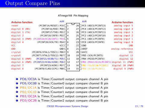
Output Compare Pins
PD6/OC0A is Timer/Counter0 output compare channel A pinPD5/OC0B is Timer/Counter0 output compare channel B pinPB1/OC1A is Timer/Counter1 output compare channel A pinPB2/OC1B is Timer/Counter1 output compare channel B pinPB3/OC2A is Timer/Counter2 output compare channel A pinPD3/OC2B is Timer/Counter2 output compare channel B pin
CN310 Microprocessor Systems Design 13 / 70

Block Diagram - 8-bit Timer/Counter
CN310 Microprocessor Systems Design 14 / 70

Block Diagram - 16-bit Timer/Counter
CN310 Microprocessor Systems Design 15 / 70
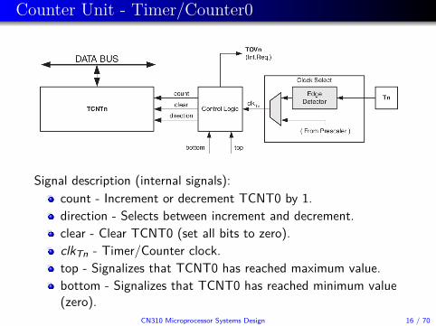
Counter Unit - Timer/Counter0
Signal description (internal signals):count - Increment or decrement TCNT0 by 1.direction - Selects between increment and decrement.clear - Clear TCNT0 (set all bits to zero).clkTn - Timer/Counter clock.top - Signalizes that TCNT0 has reached maximum value.bottom - Signalizes that TCNT0 has reached minimum value(zero).
CN310 Microprocessor Systems Design 16 / 70

Counter Unit - Timer/Counter1
Signal description (internal signals):count - Increment or decrement TCNT1 by 1.direction - Selects between increment and decrement.clear - Clear TCNT1 (set all bits to zero).clkTn - Timer/Counter clock.top - Signalizes that TCNT1 has reached maximum value.bottom - Signalizes that TCNT1 has reached minimum value(zero).
CN310 Microprocessor Systems Design 17 / 70

Counter Unit - Timer/Counter2
Signal description (internal signals):count - Increment or decrement TCNT2 by 1.direction - Selects between increment and decrement.clear - Clear TCNT2 (set all bits to zero).clkTn - Timer/Counter clock.top - Signalizes that TCNT2 has reached maximum value.bottom - Signalizes that TCNT2 has reached minimum value(zero).
CN310 Microprocessor Systems Design 18 / 70
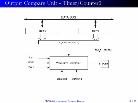
Output Compare Unit - Timer/Counter0
CN310 Microprocessor Systems Design 19 / 70
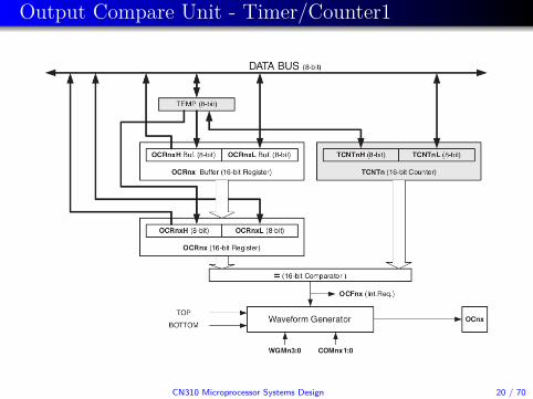
Output Compare Unit - Timer/Counter1
CN310 Microprocessor Systems Design 20 / 70

Output Compare Unit - Timer/Counter2
CN310 Microprocessor Systems Design 21 / 70

Related Registers
Summary of registers related to timers in ATmega168:
Register Name NoteTCCRnA Timer/Countern Control Register ATCCRnB Timer/Countern Control Register BTCCRnC1 Timer/Countern Control Register CTCNTn Timer/Countern Register TCNT1H, TCNT1LOCRnA Output Compare Register n A OCR1AH, OCR1ALOCRnB Output Compare Register n B OCR1BH, OCR1BLICRn2 Input Capture Register n ICR1H, ICR1LTIMSKn Timer/Countern Interrupt Mask RegisterTIFRn Timer/Countern Interrupt Flag RegisterASSRn3 Asynchronous Status Register n ASSR2GTCCR General Timer/Counter Register
1Only in Timer/Counter12Only in Timer/Counter13Only in Timer/Counter2
CN310 Microprocessor Systems Design 22 / 70

Related Registers
8-bit Timer:Timer0 Timer2 NameTCCR0A TCCR2A Timer/Counter Control Register ATCCR0B TCCR2B Timer/Counter Control Register BTCNT0 TCNT2 Timer/Counter RegisterOCR0A OCR2A Output Compare Register AOCR0B OCR2B Output Compare Register BTIMSK0 TIMSK2 Timer/Counter Interrupt Mask RegisterTIFR0 TIFR2 Timer/Counter Interrupt Flag Register
16-bit Timer:Timer1 Name NoteTCCR1A Timer/Counter Control Register ATCCR1B Timer/Counter Control Register BTCCR1C Timer/Counter Control Register CTCNT1 Timer/Counter Register TCNT1H, TCNT1LOCR1A Output Compare Register A OCR1AH, OCR1ALOCR1B Output Compare Register B OCR1BH, OCR1BLICR1 Input Capture Register ICR1H, ICR1LTIMSK1 Timer/Counter Interrupt Mask RegisterTIFR1 Timer/Counter Interrupt Flag Register
CN310 Microprocessor Systems Design 23 / 70

Operation Modes
Each timer provides 4 modes of operation:1 Normal mode.2 Clear Timer on Compare Match (CTC) mode.3 Fast PWM mode (single slope PWM).4 Phase Correct PWM mode (double slope PWM).
Two sets of flags in control registers set operation mode.Waveform Generation Mode (WGM) - control countingsequence.Compare Output Mode (COM) - control inversion of outputwith PWM or output level with compare match.
CN310 Microprocessor Systems Design 24 / 70
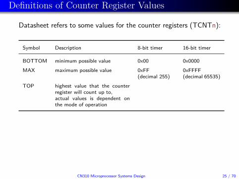
Definitions of Counter Register Values
Datasheet refers to some values for the counter registers (TCNTn):
Symbol Description 8-bit timer 16-bit timer
BOTTOM minimum possible value 0x00 0x0000MAX maximum possible value 0xFF
(decimal 255)0xFFFF(decimal 65535)
TOP highest value that the counterregister will count up to,actual values is dependent onthe mode of operation
CN310 Microprocessor Systems Design 25 / 70

Normal Mode
Operation:counter register always counts up (incrementing)no counter clear is performedcounter register counts up to MAX and restarts fromBOTTOMthe Timer Overflow Flag (TOVn) will be set in the same timerclock cycle as the TCNTn becomes zeroan interrupt can be generated with TOVn set
CN310 Microprocessor Systems Design 26 / 70
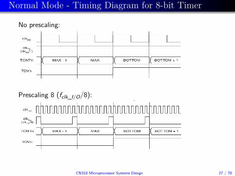
Normal Mode - Timing Diagram for 8-bit Timer
No prescaling:
Prescaling 8 (fclk_I/O/8):
CN310 Microprocessor Systems Design 27 / 70

Normal Mode - Timing Diagram for 16-bit Timer
No prescaling:
Prescaling 8 (fclk_I/O/8):
CN310 Microprocessor Systems Design 28 / 70

Normal Mode - Setting Up
General steps:disable interrupt (may not be necessary with default settings)set the WGMn (Waveform Generation Mode) flags forNormal modeset the CSn (Clock Select) flags to select clocksource/prescalerchoose other starting value instead of BOTTOM, ifappropriate, and number of required interrupts for the desiredtime durationset the TOIEn flag to enable timer overflow interruptset the I flag (in SREG) to enable global interrupt
CN310 Microprocessor Systems Design 29 / 70

Timer/Counter2 - Registers
CN310 Microprocessor Systems Design 30 / 70
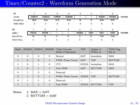
Timer/Counter2 - Waveform Generation Mode
Mode WGM22 WGM21 WGM20 Timer/CounterMode of Operation
TOP Update ofOCR2x at
TOV2 FlagSet on
0 0 0 0 Normal 0xFF Immediate MAX1 0 0 1 PWM, Phase Correct 0xFF TOP BOTTOM2 0 1 0 CTC OCR2A Immediate MAX3 0 1 1 Fast PWM 0xFF BOTTOM MAX4 1 0 0 Reserved – – –5 1 0 1 PWM, Phase Correct OCR2A TOP BOTTOM6 1 1 0 Reserved – – –7 1 1 1 Fast PWM OCR2A BOTTOM TOP
Notes: 1. MAX = 0xFF2. BOTTOM = 0x00
CN310 Microprocessor Systems Design 31 / 70

Timer/Counter2 - Clock Source/Prescaler
CN310 Microprocessor Systems Design 32 / 70
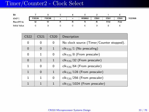
Timer/Counter2 - Clock Select
CS22 CS21 CS20 Description0 0 0 No clock source (Timer/Counter stopped).0 0 1 clkT2S/1 (No prescaling)0 1 0 clkT2S/8 (From prescaler)0 1 1 clkT2S/32 (From prescaler)1 0 0 clkT2S/64 (From prescaler)1 0 1 clkT2S/128 (From prescaler)1 1 0 clkT2S/256 (From prescaler)1 1 1 clkT2S/1024 (From prescaler)
CN310 Microprocessor Systems Design 33 / 70

Example 8.1: Timer/Counter2 - Normal Mode
1 #include <avr/io.h>2 #include <avr/interrupt.h>34 // TIMER2 overflow interrupt service routine5 ISR(TIMER2_OVF_vect) {6 // toggle PB07 PORTB ^= 1<<PB0;8 }9
CN310 Microprocessor Systems Design 34 / 70
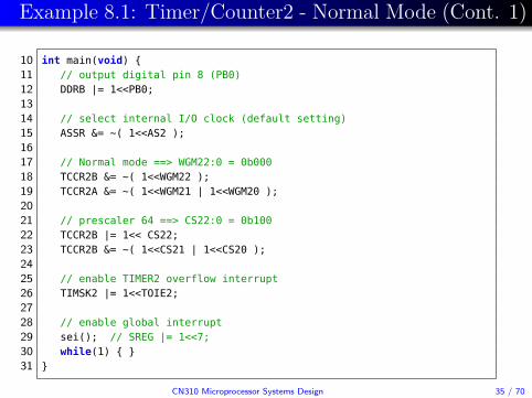
Example 8.1: Timer/Counter2 - Normal Mode (Cont. 1)
10 int main(void) {11 // output digital pin 8 (PB0)12 DDRB |= 1<<PB0;1314 // select internal I/O clock (default setting)15 ASSR &= ~( 1<<AS2 );1617 // Normal mode ==> WGM22:0 = 0b00018 TCCR2B &= ~( 1<<WGM22 );19 TCCR2A &= ~( 1<<WGM21 | 1<<WGM20 );2021 // prescaler 64 ==> CS22:0 = 0b10022 TCCR2B |= 1<< CS22;23 TCCR2B &= ~( 1<<CS21 | 1<<CS20 );2425 // enable TIMER2 overflow interrupt26 TIMSK2 |= 1<<TOIE2;2728 // enable global interrupt29 sei(); // SREG |= 1<<7;30 while(1) { }31 }
CN310 Microprocessor Systems Design 35 / 70

Example 8.1: Timer/Counter2 - Normal Mode (Cont. 2)
Working out the frequency of signal at PB0.System clock frequency: fsys = 16 MHz (fixed on Arduino board)Timer2 with prescaler = 64
frequency: fT2 = fsys/64 −→ fT2 = 16 MHz/64 = 250000 Hzperiod: TT2 = 1/fT2 −→ TT2 = 1/250000 Hz = 4 us
In this example, for Timer2 in Normal mode:start count: TCNT2 = 0 (0x00)end count: TCNT2 = 255 (0xFF)1 interrupt takes: 256 x TT2 (counting: 0 → 255 → 0 )1 period of signal at PB0 takes: 2 interrupts = 2 x 256 x TT2
Frequency of:
interrupt: finterrupt = 1256 x 4 us = 976.5625 Hz
signal at PB0: fat PB0 = 12 x 256 x 4 us = 488.28125 Hz
CN310 Microprocessor Systems Design 36 / 70

Example 8.2: Timer/Counter2 - Normal Mode
1 #include <avr/io.h>2 #include <avr/interrupt.h>34 // starting count for counter register5 // this will give 250T of Timer2 for 1 interrupt6 int reload_count = 6;78 // TIMER2 overflow interrupt service routine9 ISR(TIMER2_OVF_vect) {
10 // reload counter register11 TCNT2 = reload_count;1213 // toggle PB014 PORTB ^= 1<<PB0;15 }16
CN310 Microprocessor Systems Design 37 / 70

Example 8.2: Timer/Counter2 - Normal Mode (Cont. 1)
17 int main(void) {18 // output digital pin 8 (PB0)19 DDRB |= 1<<PB0;2021 // select internal I/O clock (default setting)22 ASSR &= ~( 1<<AS2 );2324 // Normal mode ==> WGM22:0 = 0b00025 TCCR2B &= ~( 1<<WGM22 );26 TCCR2A &= ~( 1<<WGM21 | 1<<WGM20 );2728 // prescaler 64 ==> CS22:0 = 0b10029 TCCR2B |= 1<< CS22;30 TCCR2B &= ~( 1<<CS21 | 1<<CS20 );3132 // enable TIMER2 overflow interrupt33 TIMSK2 |= 1<<TOIE2;3435 // enable global interrupt36 sei(); // SREG |= 1<<7;37 while(1) { }38 }
CN310 Microprocessor Systems Design 38 / 70

Example 8.2: Timer/Counter2 - Normal Mode (Cont. 2)
Working out the frequency of signal at PB0.System clock frequency: fsys = 16 MHz (fixed on Arduino board)Timer2 with prescaler = 64
frequency: fT2 = fsys/64 −→ fT2 = 16 MHz/64 = 250000 Hzperiod: TT2 = 1/fT2 −→ TT2 = 1/250000 Hz = 4 us
In this example, for Timer2 in Normal mode:start count: TCNT2 = 6 (0x06)end count: TCNT2 = 255 (0xFF)1 interrupt takes: 250 x TT2 (counting: 6 → 255 → 0 )1 period of signal at PB0 takes: 2 interrupts = 2 x 250 x TT2
Frequency of:
interrupt: finterrupt = 1250 x 4 us = 1 kHz
signal at PB0: fat PB0 = 12 x 250 x 4 us = 500 Hz
CN310 Microprocessor Systems Design 39 / 70
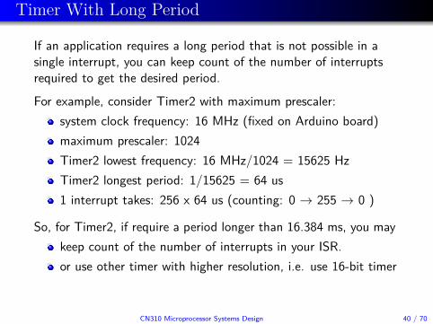
Timer With Long Period
If an application requires a long period that is not possible in asingle interrupt, you can keep count of the number of interruptsrequired to get the desired period.For example, consider Timer2 with maximum prescaler:
system clock frequency: 16 MHz (fixed on Arduino board)maximum prescaler: 1024Timer2 lowest frequency: 16 MHz/1024 = 15625 HzTimer2 longest period: 1/15625 = 64 us1 interrupt takes: 256 x 64 us (counting: 0 → 255 → 0 )
So, for Timer2, if require a period longer than 16.384 ms, you maykeep count of the number of interrupts in your ISR.or use other timer with higher resolution, i.e. use 16-bit timer
CN310 Microprocessor Systems Design 40 / 70

Example 8.3: Timer/Counter2 - Normal Mode withLong Period
Program: Toggle the LED every 1 second.
In this case:desired period of 1 s is longer than 16.384 ms (for Timer2)we will keep count of the number of interrupts
CN310 Microprocessor Systems Design 41 / 70

Example 8.3: Timer/Counter2 - Normal Mode withLong Period
For Timer2:system clock frequency: 16 MHz (fixed on Arduino board)choose prescaler: 256frequency: fT2 = fsys/256 −→ fT2 = 16 MHz/256 = 62500 Hzperiod: TT2 = 1/fT2 −→ TT2 = 1/62500 Hz = 16 uschoose 1 interrupt for every: 100 x TT2 (counting: 156 → 255 → 0)
number of interrupts required for 1 S: 1 S100 x 16 us = 625
CN310 Microprocessor Systems Design 42 / 70
Example 8.3: Timer/Counter2 - Normal Mode withLong Period
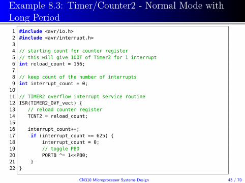
1 #include <avr/io.h>2 #include <avr/interrupt.h>34 // starting count for counter register5 // this will give 100T of Timer2 for 1 interrupt6 int reload_count = 156;78 // keep count of the number of interrupts9 int interrupt_count = 0;
1011 // TIMER2 overflow interrupt service routine12 ISR(TIMER2_OVF_vect) {13 // reload counter register14 TCNT2 = reload_count;1516 interrupt_count++;17 if (interrupt_count == 625) {18 interrupt_count = 0;19 // toggle PB020 PORTB ^= 1<<PB0;21 }22 }
CN310 Microprocessor Systems Design 43 / 70

Example 8.3: Timer/Counter2 - Normal Mode withLong Period (Cont. 1)24 int main(void) {25 // output digital pin 8 (PB0)26 DDRB |= 1<<PB0;2728 // select internal I/O clock (default setting)29 ASSR &= ~( 1<<AS2 );3031 // Normal mode ==> WGM22:0 = 0b00032 TCCR2B &= ~( 1<<WGM22 );33 TCCR2A &= ~( 1<<WGM21 | 1<<WGM20 );3435 // prescaler 256 ==> CS22:0 = 0b11036 TCCR2B |= (1<< CS22 | 1<<CS21);37 TCCR2B &= ~( 1<<CS20 );3839 // enable TIMER2 overflow interrupt40 TIMSK2 |= 1<<TOIE2;4142 // enable global interrupt43 sei(); // SREG |= 1<<7;44 while(1) { }45 }
CN310 Microprocessor Systems Design 44 / 70
Example 8.3: Timer/Counter2 - Normal Mode withLong Period (Cont. 2)
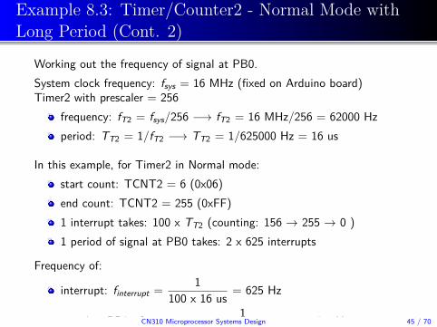
Working out the frequency of signal at PB0.System clock frequency: fsys = 16 MHz (fixed on Arduino board)Timer2 with prescaler = 256
frequency: fT2 = fsys/256 −→ fT2 = 16 MHz/256 = 62000 Hzperiod: TT2 = 1/fT2 −→ TT2 = 1/625000 Hz = 16 us
In this example, for Timer2 in Normal mode:start count: TCNT2 = 6 (0x06)end count: TCNT2 = 255 (0xFF)1 interrupt takes: 100 x TT2 (counting: 156 → 255 → 0 )1 period of signal at PB0 takes: 2 x 625 interrupts
Frequency of:
interrupt: finterrupt = 1100 x 16 us = 625 Hz
signal at PB0: fat PB0 = 12 x 625 x 100 x 16 us = 0.5 HzCN310 Microprocessor Systems Design 45 / 70

Timer/Counter1 - Registers
CN310 Microprocessor Systems Design 46 / 70

Timer/Counter1 - Waveform Generation Mode
Mode WGM13 WGM12 WGM11 WGM10 Timer/CounterMode of Operation
TOP Update ofOCR1x at
TOV1 FlagSet on
0 0 0 0 0 Normal 0xFFFF Immediate MAX1 0 0 0 1 PWM, Phase Correct, 8-bit 0x00FF TOP BOTTOM2 0 0 1 0 PWM, Phase Correct, 9-bit 0x01FF TOP BOTTOM3 0 0 1 1 PWM, Phase Correct, 10-bit 0x03FF TOP BOTTOM4 0 1 0 0 CTC OCR1A Immediate MAX5 0 1 0 1 Fast PWM, 8-bit 0x00FF BOTTOM TOP6 0 1 1 0 Fast PWM, 9-bit 0x01FF BOTTOM TOP7 0 1 1 1 Fast PWM, 10-bit 0x03FF BOTTOM TOP8 1 0 0 0 PWM, Phase and Frequency
CorrectICR1 BOTTOM BOTTOM
9 1 0 0 1 PWM, Phase and FrequencyCorrect
OCR1A BOTTOM BOTTOM
10 1 0 1 0 PWM, Phase Correct ICR1 TOP BOTTOM11 1 0 1 1 PWM, Phase Correct OCR1A TOP BOTTOM12 1 1 0 0 CTC ICR1 Immediate MAX13 1 1 0 1 Reserved – – –14 1 1 1 0 Fast PWM ICR1 BOTTOM TOP15 1 1 1 1 Fast PWM OCR1A BOTTOM TOP
Notes: 1. MAX = 0xFFFF2. BOTTOM = 0x0000
CN310 Microprocessor Systems Design 47 / 70

Timer/Counter1 - Clock Source/Prescaler
Note that Timer1 shares prescaler with Timer0.
CN310 Microprocessor Systems Design 48 / 70
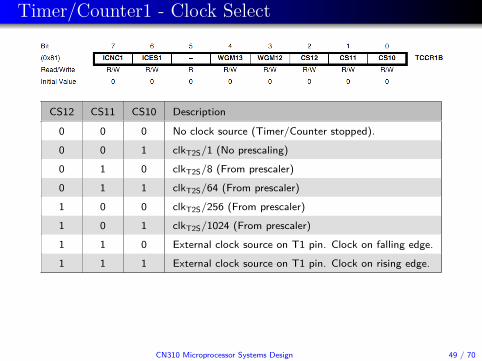
Timer/Counter1 - Clock Select
CS12 CS11 CS10 Description0 0 0 No clock source (Timer/Counter stopped).0 0 1 clkT2S/1 (No prescaling)0 1 0 clkT2S/8 (From prescaler)0 1 1 clkT2S/64 (From prescaler)1 0 0 clkT2S/256 (From prescaler)1 0 1 clkT2S/1024 (From prescaler)1 1 0 External clock source on T1 pin. Clock on falling edge.1 1 1 External clock source on T1 pin. Clock on rising edge.
CN310 Microprocessor Systems Design 49 / 70

Example 8.4: Timer/Counter1 - Normal Mode
1 #include <avr/io.h>2 #include <avr/interrupt.h>34 // starting count for counter register5 int reload_count = 3036;67 // TIMER1 overflow interrupt service routine8 ISR(TIMER1_OVF_vect) {9 // reload counter register
10 TCNT1 = reload_count;1112 // toggle PB013 PORTB ^= 1<<PB0;14 }15
CN310 Microprocessor Systems Design 50 / 70

Example 8.4: Timer/Counter1 - Normal Mode (Cont. 1)
16 int main(void) {17 // output digital pin 8 (PB0)18 DDRB |= 1<<PB0;1920 // Normal mode ==> WGM13:0 = 0b000021 TCCR1B &= ~( 1<<WGM13 | 1<<WGM12 );22 TCCR1A &= ~( 1<<WGM11 | 1<<WGM10 );2324 // prescaler 256 ==> CS12:0 = 0b10025 TCCR1B |= 1<< CS12;26 TCCR1B &= ~( 1<<CS11 | 1<<CS10 );2728 // enable TIMER1 overflow interrupt29 TIMSK1 |= 1<<TOIE1;3031 // enable global interrupt32 sei(); // SREG |= 1<<7;33 while(1) { }34 }
CN310 Microprocessor Systems Design 51 / 70
Example 8.4: Timer/Counter1 - Normal Mode (Cont. 2)
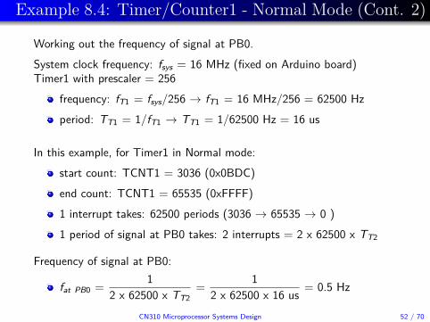
Working out the frequency of signal at PB0.System clock frequency: fsys = 16 MHz (fixed on Arduino board)Timer1 with prescaler = 256
frequency: fT1 = fsys/256 → fT1 = 16 MHz/256 = 62500 Hzperiod: TT1 = 1/fT1 → TT1 = 1/62500 Hz = 16 us
In this example, for Timer1 in Normal mode:start count: TCNT1 = 3036 (0x0BDC)end count: TCNT1 = 65535 (0xFFFF)1 interrupt takes: 62500 periods (3036 → 65535 → 0 )1 period of signal at PB0 takes: 2 interrupts = 2 x 62500 x TT2
Frequency of signal at PB0:
fat PB0 = 12 x 62500 x TT2
= 12 x 62500 x 16 us = 0.5 Hz
CN310 Microprocessor Systems Design 52 / 70

Clear Timer on Compare Match (CTC) Mode
Operation:counter register always counts up (incrementing)counter register counts up TOP value
TOP value is OCR0A in Timer0TOP value is OCR2A in Timer2TOP value is either OCR1A or ICR1A in Timer1
when counter value (TCNTn) matches TOP value, thecounter register (TCNTn) is cleared to zerothe Output Compare Match Flag (OCFnA) will be set in thesame timer clock cycle as the TCNTn becomes zeroan interrupt can be generated with TOVn set
CN310 Microprocessor Systems Design 53 / 70

CTC Mode - Timing Diagram for 8-bit Timer
CN310 Microprocessor Systems Design 54 / 70

CTC Mode - Timing Diagram for 8-bit Timer
Prescaling 8 (fclk_I/O/8):
CN310 Microprocessor Systems Design 55 / 70

CTC Mode - Timing Diagram for 16-bit Timer
CN310 Microprocessor Systems Design 56 / 70

CTC Mode - Timing Diagram for 16-bit Timer
Prescaling 8 (fclk_I/O/8):
CN310 Microprocessor Systems Design 57 / 70

CTC Mode - Setting Up
General steps:disable interrupt (may not be necessary with default settings)set the WGMn (Waveform Generation Mode) flags for CTCmodeset the CSn (Clock Select) flags to select clocksource/prescalerchoose value for TOP (assign the value to either OCRnA orICR1A)set the OCFn flag to enable output compare match interruptset the I flag (in SREG) to enable global interrupt
As in Normal mode, the TOVn Flag is set in the same timer clockcycle that the counter counts from MAX to BOTTOM.
CN310 Microprocessor Systems Design 58 / 70

Example 8.5: Timer/Counter2 - CTC Mode
1 #include <avr/io.h>2 #include <avr/interrupt.h>34 // TIMER2 compare match channel A interrupt service routine5 ISR(TIMER2_COMPA_vect) {6 // toggle PB07 PORTB ^= 1<<PB0;8 }9
CN310 Microprocessor Systems Design 59 / 70

Example 8.5: Timer/Counter2 - CTC Mode (Cont. 1)
10 int main(void) {11 // output digital pin 8 (PB0)12 DDRB |= 1<<PB0;1314 // select internal I/O clock (default setting)15 ASSR &= ~( 1<<AS2 );16 // CTC mode ==> WGM22:0 = 0b01017 TCCR2B &= ~( 1<<WGM22 );18 TCCR2A |= 1<<WGM21;19 TCCR2A &= ~( 1<<WGM20 );20 // prescaler 64 ==> CS22:0 = 0b10021 TCCR2B |= 1<< CS22;22 TCCR2B &= ~( 1<<CS21 | 1<<CS20 );23 // set output compare register (OCR2A) - interrupt every 100T24 OCR2A = 99;25 // enable TIMER2 output compare match interrupt26 TIMSK2 |= 1<<OCIE2A;27 // enable global interrupt28 sei(); // SREG |= 1<<7;29 while(1) { }30 }
CN310 Microprocessor Systems Design 60 / 70

Example 8.5: Timer/Counter2 - CTC Mode (Cont. 2)
Working out the frequency of signal at PB0.System clock frequency: fsys = 16 MHz (fixed on Arduino board)Timer1 with prescaler = 64
frequency: fT2 = fsys/64 −→ fT2 = 16 MHz/64 = 250000 Hzperiod: TT2 = 1/fT2 −→ TT2 = 1/250000 Hz = 4 us
In this example, for Timer2 in CTC mode:start count: TCNT2 = 0 (0x00)end count: TCNT2 = OCR2A = 99 (0x63)1 interrupt takes 100 periods (0 → 99 → 0 )1 period of signal at PB0 takes 2 interrupts: 2 x 100 x TT2
Frequency of:interrupt: 1
100 x 4 us = 2500 Hz
signal at PB0: fat PB0 = 12 x 100 x 4 us = 1250 Hz
CN310 Microprocessor Systems Design 61 / 70

Using Output Compare Unit
On compare match between Counter register (TCNTn) andOutput Compare register (OCRnx), the output compare unit cangenerate signal on the Output Compare pin (OCnx).
Each timer controls 2 output compare pins (channel A and B)
Timer/Counter0 controls: PD6/OC0A and PD5/OC0BTimer/Counter1 controls: PB1/OC1A and PB2/OC1BTimer/Counter2 controls: PB3/OC2A and PD3/OC2B
CN310 Microprocessor Systems Design 62 / 70
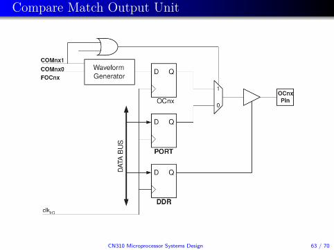
Compare Match Output Unit
CN310 Microprocessor Systems Design 63 / 70

Compare Match Output Unit
The Waveform Generator uses the Compare Output Mode flags(COMnx) to define the state of the Output Compare pins (OCnx).
To use the Output Compare pins (OCnx), the DDR bit for theOCnx pin must be set as output before the OCnx value is visibleon the pin.
The Waveform Generator uses the COMnx bits differently innormal, CTC, and PWM modes.
CN310 Microprocessor Systems Design 64 / 70

Timer/Counter2 - Compare Output Mode
COM2A1 COM2A0 Description0 0 Normal port operation, OC2A disconnected.0 1 Toggle OC2A on Compare Match1 0 Clear OC2A on Compare Match1 1 Set OC2A on Compare Match
Compare Output Mode, non-PWM Mode
COM2B1 COM2B0 Description0 0 Normal port operation, OC2B disconnected.0 1 Toggle OC2B on Compare Match1 0 Clear OC2B on Compare Match1 1 Set OC2B on Compare Match
Compare Output Mode, non-PWM Mode
CN310 Microprocessor Systems Design 65 / 70

Example 8.6: Timer/Counter2 - Use OC2A in CTC
Program: Generate square wave on OC2A with frequency of 1 kHz.
Timer2 with prescaler = 64frequency: fT2 = fsys/64 −→ fT2 = 16 MHz/64 = 250000 Hzperiod: TT2 = 1/fT2 −→ TT2 = 1/250000 Hz = 4 us
Use toggle output on compare match.desired output period: 1/1000 = 1 msfor toggle output mode, should toggle for every 0.5 msrequired number of periods: 0.5 ms / 4 us = 125value for OCR2A: 124 (counting: 0 → 124 → 0)
Note that interrupt will not be used.
CN310 Microprocessor Systems Design 66 / 70

Example 8.6: Timer/Counter2 - Use OC1A in CTC
1 #include <avr/io.h>2 #include <avr/interrupt.h>34 int main(void) {5 // OC2A pin, digital pin 11 (PB3)6 DDRB |= 1<<PB3;7 // set compare ouput mode to toggle ==> COM2A1:0 = 0b018 TCCR2A &= ~( 1<<COM2A1 );9 TCCR2A |= 1<<COM2A0;
10 // select internal I/O clock (default setting)11 ASSR &= ~( 1<<AS2 );12 // CTC mode ==> WGM22:0 = 0b01013 TCCR2B &= ~( 1<<WGM22 );14 TCCR2A |= 1<<WGM21;15 TCCR2A &= ~( 1<<WGM20 );16 // prescaler 64 ==> CS22:0 = 0b10017 TCCR2B |= 1<< CS22;18 TCCR2B &= ~( 1<<CS21 | 1<<CS20 );19 // set output compare register (OCR2A)20 OCR2A = 124;21 while(1) { }22 }
CN310 Microprocessor Systems Design 67 / 70

Timer/Counter1 - Compare Output Mode
COM1A1/COM1B1 COM1A0/COM1B0 Description0 0 Normal port operation, OC1A/OC1B
disconnected.0 1 Toggle OC1A/OC1B on Compare
Match.1 0 Clear OC1A/OC1B on Compare Match
(Set output to low level).1 1 Set OC1A/OC1B on Compare Match
(Set output to high level).
Compare Output Mode, non-PWM Mode
CN310 Microprocessor Systems Design 68 / 70

Example 8.7: Timer/Counter1 - Use OC1A in CTC
Program: Generate square wave on OC1A with frequency of 50 Hz.
Timer1 with prescaler = 64frequency: fT2 = fsys/64 −→ fT2 = 16 MHz/64 = 250000 Hzperiod: TT2 = 1/fT2 −→ TT2 = 1/250000 Hz = 4 us
Use toggle output on compare match.desired output period: 1/50 = 20 msfor toggle output mode, should toggle for every 10 msrequired number of periods: 10 ms / 4 us = 2500value for OCR1A: 2499 (counting: 0 → 2499 → 0)
Note that interrupt will not be used.
CN310 Microprocessor Systems Design 69 / 70
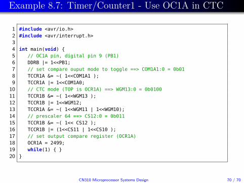
Example 8.7: Timer/Counter1 - Use OC1A in CTC
1 #include <avr/io.h>2 #include <avr/interrupt.h>34 int main(void) {5 // OC1A pin, digital pin 9 (PB1)6 DDRB |= 1<<PB1;7 // set compare ouput mode to toggle ==> COM1A1:0 = 0b018 TCCR1A &= ~( 1<<COM1A1 );9 TCCR1A |= 1<<COM1A0;
10 // CTC mode (TOP is OCR1A) ==> WGM13:0 = 0b010011 TCCR1B &= ~( 1<<WGM13 );12 TCCR1B |= 1<<WGM12;13 TCCR1A &= ~( 1<<WGM11 | 1<<WGM10);14 // prescaler 64 ==> CS12:0 = 0b01115 TCCR1B &= ~( 1<< CS12 );16 TCCR1B |= (1<<CS11 | 1<<CS10 );17 // set output compare register (OCR1A)18 OCR1A = 2499;19 while(1) { }20 }
CN310 Microprocessor Systems Design 70 / 70
Related Documents