KIT – University of the State of Baden-Wuerttemberg and National Research Center of the Helmholtz Association Institut für Experimentelle Kernphysik www.kit.edu CMS Phase II Tracker Upgrade GRK-Workshop in Bad Liebenzell 8.10. – 10.10.2012 Robert Eber

Welcome message from author
This document is posted to help you gain knowledge. Please leave a comment to let me know what you think about it! Share it to your friends and learn new things together.
Transcript

KIT – University of the State of Baden-Wuerttemberg and
National Research Center of the Helmholtz Association
Institut für Experimentelle Kernphysik
www.kit.edu
CMS Phase II Tracker Upgrade GRK-Workshop in Bad Liebenzell 8.10. – 10.10.2012
Robert Eber

GRK-Workshop Bad Liebenzell 2
8.10. – 10.10.2012
Robert Eber
Institut für Experimentelle Kernphysik, KIT
Higgs candidate ZZ event (8TeV) with 2 µ and 2 e
Upgrade?
GRK-Workshop Bad Liebenzell 3
8.10. – 10.10.2012
Robert Eber
Institut für Experimentelle Kernphysik, KIT
Outline
CMS Overview
Tracker
Phase II Tracker Upgrade
HPK Campaign
Radiation Hardness
Sensor Qualification
Tracker Trigger Concept
Summary

GRK-Workshop Bad Liebenzell 4
8.10. – 10.10.2012
Robert Eber
Institut für Experimentelle Kernphysik, KIT
Compact Muon Solenoid (CMS) Experiment
Silicon
Detectors Measure tracks left
by charged particles
Calorimeters Absorb particles and
measure their
energy
Muon
Detectors Identify and
measure muons that
penetrate
3.8 T Magnet Bend tracks of
charged particles
z
GRK-Workshop Bad Liebenzell 5
8.10. – 10.10.2012
Robert Eber
Institut für Experimentelle Kernphysik, KIT
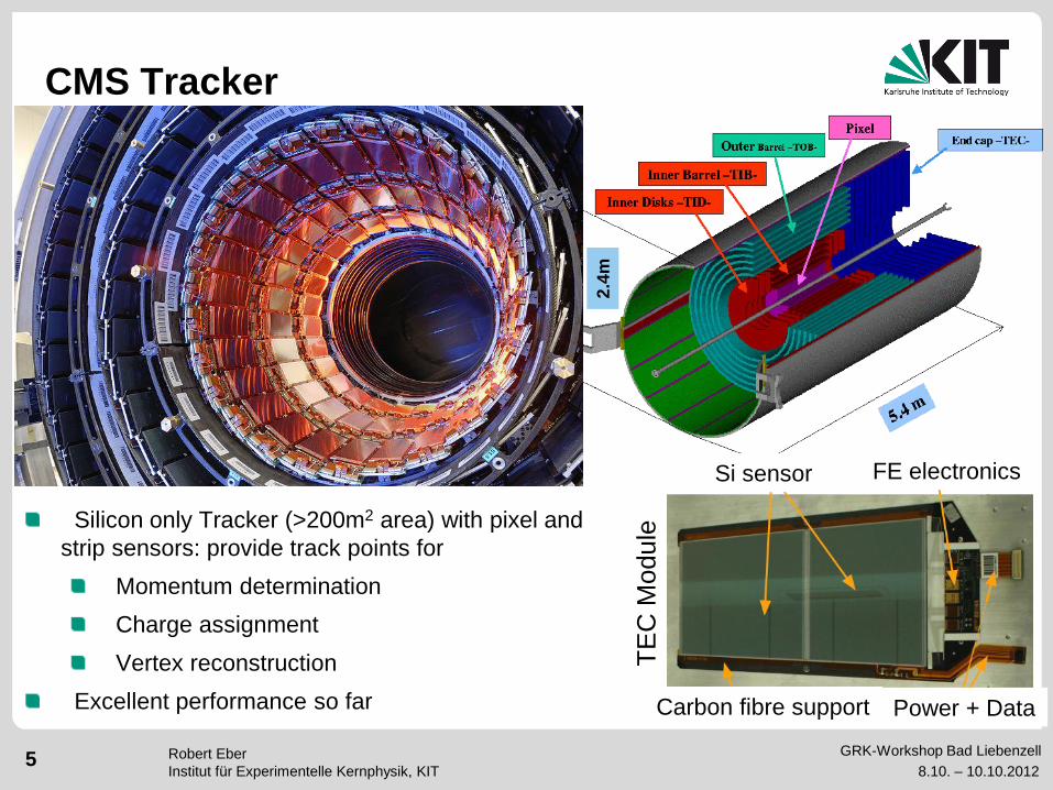
CMS Tracker
Silicon only Tracker (>200m2 area) with pixel and
strip sensors: provide track points for
Momentum determination
Charge assignment
Vertex reconstruction
Excellent performance so far
2.4
m
Si sensor FE electronics
Carbon fibre support Power + Data
TE
C M
odule

GRK-Workshop Bad Liebenzell 6
8.10. – 10.10.2012
Robert Eber
Institut für Experimentelle Kernphysik, KIT
65 reconstructed vertices

GRK-Workshop Bad Liebenzell 7
8.10. – 10.10.2012
Robert Eber
Institut für Experimentelle Kernphysik, KIT
Silicon (Strip) Sensor
F. Hartmann, Evolution of Silicon Sensor Technology
in Particle Detectors, Springer 2008
Design
Mini strip test sensor
(2.5x3.5cm2)
Diode (7x7mm2)
GRK-Workshop Bad Liebenzell 8
8.10. – 10.10.2012
Robert Eber
Institut für Experimentelle Kernphysik, KIT
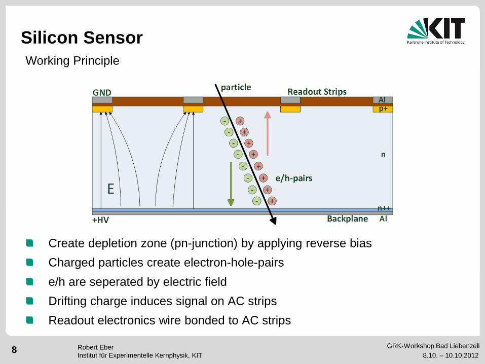
Silicon Sensor
Create depletion zone (pn-junction) by applying reverse bias
Charged particles create electron-hole-pairs
e/h are seperated by electric field
Drifting charge induces signal on AC strips
Readout electronics wire bonded to AC strips
Working Principle
GRK-Workshop Bad Liebenzell 9
8.10. – 10.10.2012
Robert Eber
Institut für Experimentelle Kernphysik, KIT
UPGRADE OF THE CMS TRACKER
GRK-Workshop Bad Liebenzell 10
8.10. – 10.10.2012
Robert Eber
Institut für Experimentelle Kernphysik, KIT
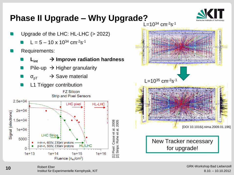
Phase II Upgrade – Why Upgrade?
Upgrade of the LHC: HL-LHC (> 2022)
L = 5 – 10 x 1034 cm-2s-1
Requirements:
Lint Improve radiation hardness
Pile-up Higher granularity
σpT Save material
L1 Trigger contribution
L=1034 cm-2s-1
L=1035 cm-2s-1
New Tracker necessary
for upgrade!
[1] P
ixel: C
asse
et al. 2
008
[2] S
trip
s: R
ohe e
t al. 2
005
[DOI 10.1016/j.nima.2009.01.196]

GRK-Workshop Bad Liebenzell 11
8.10. – 10.10.2012
Robert Eber
Institut für Experimentelle Kernphysik, KIT
Upgrade Activities –
Radiation Hard Silicon Sensors
Campagne in the scope of the CMS Tracker Collaboration (17 Institutes)
162 6"-wafers with several sensors and test structures from one manufacturer
Floatzone (FZ), Magnetic Czochralski (MCz) and Epitaxial (Epi) Silicon
Different thicknesses from 320µm (current inner tracker) down to 50µm;
current baseline: 200µm to reduce radiation length
N-bulk and p-bulk silicon
Choose 5 radii for irradiations
[M. Guthoff,2012]
@3000fb-1
Diodes
Sensors
Geometry
New layouts

GRK-Workshop Bad Liebenzell 12
8.10. – 10.10.2012
Robert Eber
Institut für Experimentelle Kernphysik, KIT
Defects
The reason for sensor degradation: Defects
Radiation damage introduces defects in the silicon crystal: forming of energy
levels in the bandgap
Effects
Increase of leakage current (a)
Generation of space charge (b) – Increase of depletion voltage
Trapping of charge carriers (c) – Reduction of signal and collected charge
Vacancy and interstitial atom
(a) (b) (c)

GRK-Workshop Bad Liebenzell 13
8.10. – 10.10.2012
Robert Eber
Institut für Experimentelle Kernphysik, KIT
Sensor Qualification
Measure Characteristics
Strip measurements
Rbias, RStrip, Ccouple, IStrip, Idiel
Interstrip Capacitance (electronics
noise for chip)
Karlsruhe Probe Station
Before irradiation
After irradiation
Depletion Voltage
Current-Voltage
Capacitance
-Voltage
GRK-Workshop Bad Liebenzell 14
8.10. – 10.10.2012
Robert Eber
Institut für Experimentelle Kernphysik, KIT
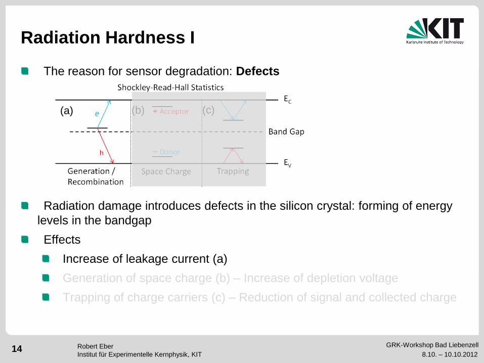
Radiation Hardness I
The reason for sensor degradation: Defects
Radiation damage introduces defects in the silicon crystal: forming of energy
levels in the bandgap
Effects
Increase of leakage current (a)
Generation of space charge (b) – Increase of depletion voltage
Trapping of charge carriers (c) – Reduction of signal and collected charge
(a) (b) (c)

GRK-Workshop Bad Liebenzell 15
8.10. – 10.10.2012
Robert Eber
Institut für Experimentelle Kernphysik, KIT
0.0 5.0x10 14
1.0x10 15
1.5x10 15
0.00
0.02
0.04
0.06
0.08
0.10
FZ320N
FZ320P
FZ200N
FZ200P
MCZ200N
MCZ200P
D I/
V (
A/c
m²)
Fluence (n eq
/cm²)
Radiation Hardness I – Alpha Factor
Increase of leakage current
proportional to fluence:
radiation damage factor α
Current in both n- and p-type
material scale the same
Cooling power estimation at 0°C
and F=1e15neq/cm2
CO2 cooling at -20°C foreseen in
phase II upgrade
Cool additional thermal power
At lower T lower ΔI
Prevent / control annealing
Δ𝐼
𝑉= 𝛼 ⋅ F𝑒𝑞
p n
[Sabine Frech]
Δ𝐼 = 0.008𝐴
𝑐𝑚3 × 200µ𝑚 × 200𝑚2
= 3.2𝐴
𝑈 = 600𝑉
Δ𝑃 = 𝑈 × Δ𝐼 = 1.9𝑘𝑊
p+n
T=20°C
expectation

GRK-Workshop Bad Liebenzell 16
8.10. – 10.10.2012
Robert Eber
Institut für Experimentelle Kernphysik, KIT
Radiation Hardness II
The reason for sensor degradation: Defects
Radiation damage introduces defects in the silicon crystal: forming of energy
levels in the bandgap
Effects
Increase of leakage current (a)
Generation of space charge (b) – Increase of depletion voltage
Trapping of charge carriers (c) – Reduction of signal and collected charge
(a) (b) (c) Irradiation
creates more
acceptor like
defects

GRK-Workshop Bad Liebenzell 17
8.10. – 10.10.2012
Robert Eber
Institut für Experimentelle Kernphysik, KIT
Depletion Voltage increases after (high) irradiation
Vdep in p-bulk sensors increases faster due to acceptor like defects
Short annealing reduces depletion voltage, long annealing increases Vdep
Sensors above 1000V could not be depleted any more
Radiation Hardness II – Depletion Voltage
T=20°C
f=1kHz
>1000V
p
n
Longer annealing (5d@RT)
p+n

GRK-Workshop Bad Liebenzell 18
8.10. – 10.10.2012
Robert Eber
Institut für Experimentelle Kernphysik, KIT
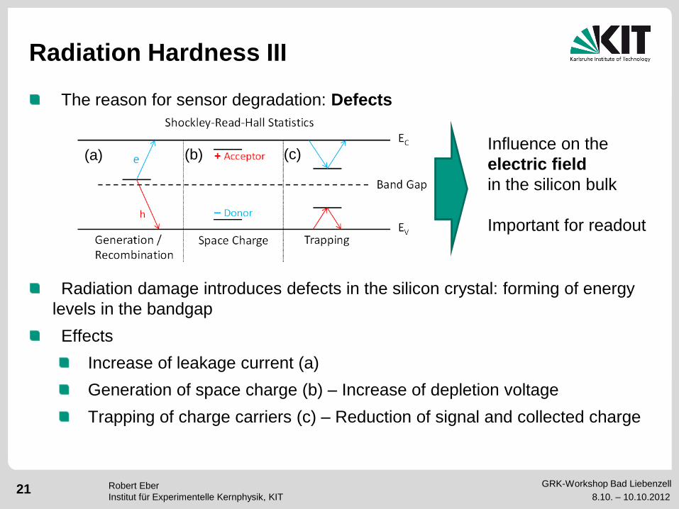
Radiation Hardness III
The reason for sensor degradation: Defects
Radiation damage introduces defects in the silicon crystal: forming of energy
levels in the bandgap
Effects
Increase of leakage current (a)
Generation of space charge (b) – Increase of depletion voltage
Trapping of charge carriers (c) – Reduction of signal and collected charge
(a) (b) (c)

GRK-Workshop Bad Liebenzell 19
8.10. – 10.10.2012
Robert Eber
Institut für Experimentelle Kernphysik, KIT
Pt100
HV
Strip Readout Sytem (Signal) – ALiBaVa
XYZ stage
Collimator for 90Sr
source
Sensor
Daughterboard
Peltier cooling
Primary cooling
Scintillator (trigger)
Isolation and shielding

GRK-Workshop Bad Liebenzell 20
8.10. – 10.10.2012
Robert Eber
Institut für Experimentelle Kernphysik, KIT
Radiation Hardness III – Electron Signal
S/N is important for final readout chip
Noise is better in thinner sensors (less leakage current)
Noise of ALiBaVa comparable to CBC
p n p+n
MIP creates ~80 e/h pairs
per µm silicon
Thinner materials lower
signals
320µm recover more
signal at 900V Signal
lower at 600V
FZ320N doesn't work at
1.5e15neq/cm2
900V
0 2 4 6 8 10 12 14 16 18
10000
15000
20000
25000
Sig
na
l (e
lec
tro
ns)
Fluence (1e14n eq /cm²)
FZ320N 900V FZ200N 900V M200N 900V FZ320P 900V FZ200P 900V M200P 900V
GRK-Workshop Bad Liebenzell 21
8.10. – 10.10.2012
Robert Eber
Institut für Experimentelle Kernphysik, KIT
Radiation Hardness III
The reason for sensor degradation: Defects
Radiation damage introduces defects in the silicon crystal: forming of energy
levels in the bandgap
Effects
Increase of leakage current (a)
Generation of space charge (b) – Increase of depletion voltage
Trapping of charge carriers (c) – Reduction of signal and collected charge
(a) (b) (c) Influence on the
electric field
in the silicon bulk
Important for readout
GRK-Workshop Bad Liebenzell 22
8.10. – 10.10.2012
Robert Eber
Institut für Experimentelle Kernphysik, KIT
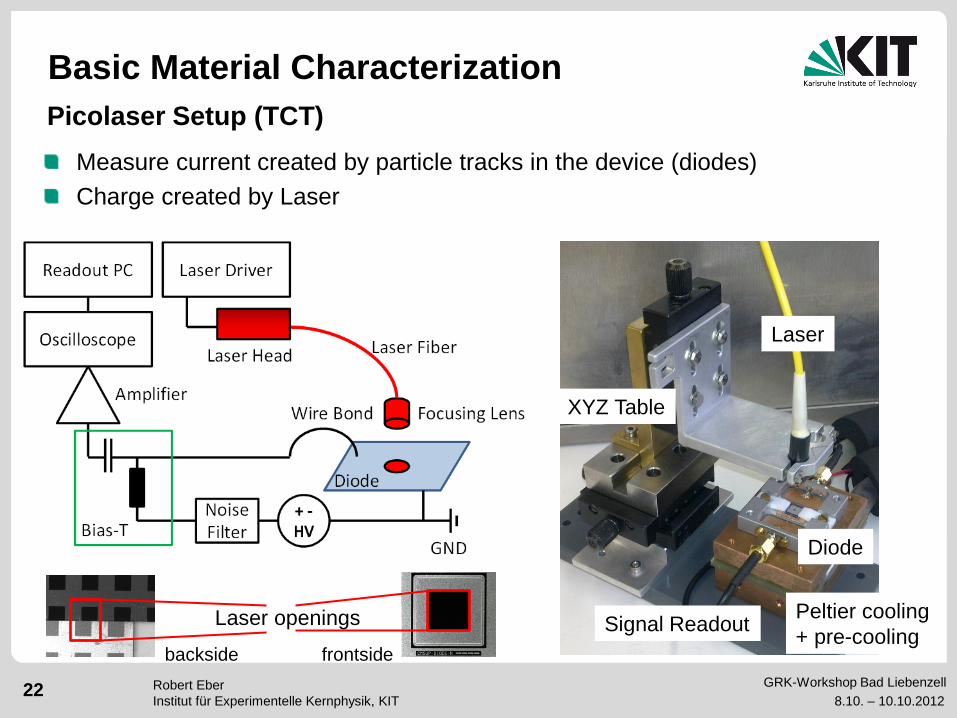
Basic Material Characterization
Picolaser Setup (TCT)
Measure current created by particle tracks in the device (diodes)
Charge created by Laser
Laser
Diode
Peltier cooling
+ pre-cooling
XYZ Table
Signal Readout
Sketch of TCT
Laser openings
backside frontside

GRK-Workshop Bad Liebenzell 23
8.10. – 10.10.2012
Robert Eber
Institut für Experimentelle Kernphysik, KIT
Transient Current Technique (TCT)
Red Laser (680nm) generates charge carriers just beneath the surface
absorption length ~4µm
Observe drift of charge carriers (current) of only one type through the diode
Measurements in unirradiated diodes show
expected electric fields
𝑣𝑑𝑟 ∝ 𝐸
Electrons, fast Holes, slow
E
Y
U1
U2
, 𝑣𝑑𝑟 < 𝑣𝑚𝑎𝑥

GRK-Workshop Bad Liebenzell 24
8.10. – 10.10.2012
Robert Eber
Institut für Experimentelle Kernphysik, KIT
TCT in Irradiated Diodes
After irradiation: electric field in the bulk changes
Stepwise reconstruction of the electric field in a diode
E-field is pulled towards the backside
Strips at frontside won't see full charge
At higher voltages, low field region vanishes
E-field
E (
V/m
)
Unirradiated case
F=1014neq/cm2
25ns
Higher fluences:
double peak
visible at higher
voltages

GRK-Workshop Bad Liebenzell 25
8.10. – 10.10.2012
Robert Eber
Institut für Experimentelle Kernphysik, KIT
UPGRADE – TRIGGER CONCEPT
GRK-Workshop Bad Liebenzell 26
8.10. – 10.10.2012
Robert Eber
Institut für Experimentelle Kernphysik, KIT
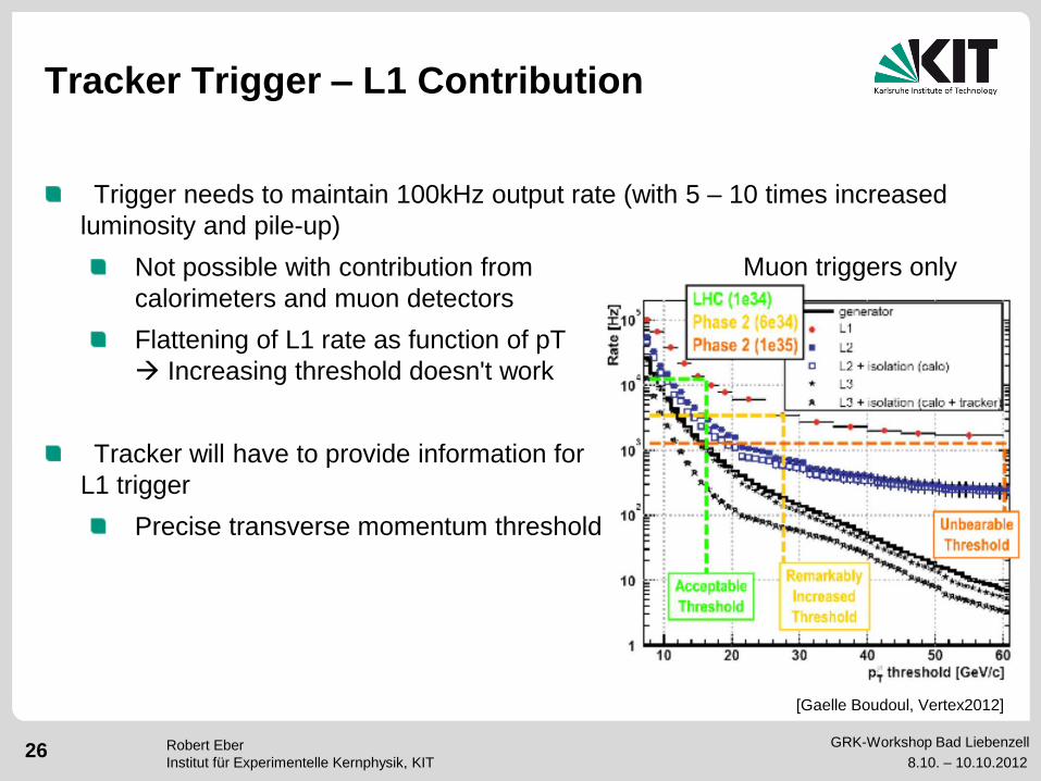
Tracker Trigger – L1 Contribution
Trigger needs to maintain 100kHz output rate (with 5 – 10 times increased
luminosity and pile-up)
Not possible with contribution from
calorimeters and muon detectors
Flattening of L1 rate as function of pT
Increasing threshold doesn't work
Tracker will have to provide information for
L1 trigger
Precise transverse momentum threshold
[Gaelle Boudoul, Vertex2012]
Muon triggers only
GRK-Workshop Bad Liebenzell 27
8.10. – 10.10.2012
Robert Eber
Institut für Experimentelle Kernphysik, KIT
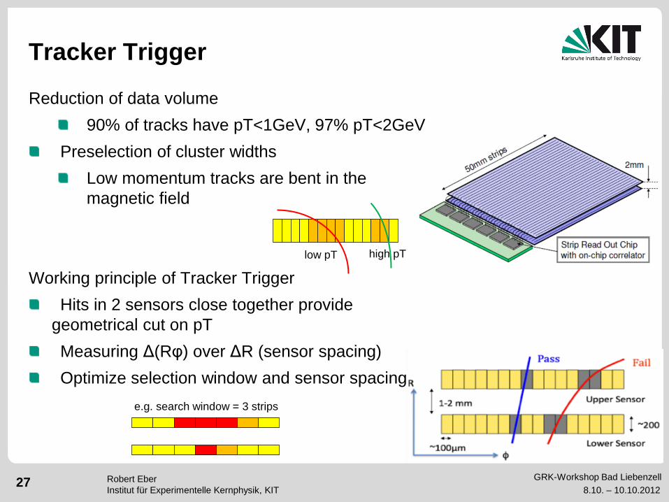
Tracker Trigger
Reduction of data volume
90% of tracks have pT<1GeV, 97% pT<2GeV
Preselection of cluster widths
Low momentum tracks are bent in the
magnetic field
Working principle of Tracker Trigger
Hits in 2 sensors close together provide
geometrical cut on pT
Measuring Δ(Rφ) over ΔR (sensor spacing)
Optimize selection window and sensor spacing
low pT high pT
e.g. search window = 3 strips

GRK-Workshop Bad Liebenzell 28
8.10. – 10.10.2012
Robert Eber
Institut für Experimentelle Kernphysik, KIT
Track Trigger Modules
Stacked sensor modules
Correlation between hits in 2 sensors close
together
Strips read out at the edge
Correlation done on the chips
Cut in X-Y plane allows to select pT treshold
2 Modules foreseen for the Tracker
2 Strip Sensors pT module
Pixel + Strip pT module

GRK-Workshop Bad Liebenzell 29
8.10. – 10.10.2012
Robert Eber
Institut für Experimentelle Kernphysik, KIT
Light Modules
Light modules
Thin silicon sensors (main contribution to material budget)
New sensor designs
Integrated pitch adapters on the sensors

GRK-Workshop Bad Liebenzell 30
8.10. – 10.10.2012
Robert Eber
Institut für Experimentelle Kernphysik, KIT
CMS Tracker Layout
2 Designs for the CMS Tracker
1. Built of trigger modules only
Inner radii: PS module
Outer radii: 2S module
2. Long barrel geometry
(no end caps)
VPS modules only: like PS
modules with vertical
interconnector

GRK-Workshop Bad Liebenzell 31
8.10. – 10.10.2012
Robert Eber
Institut für Experimentelle Kernphysik, KIT
SUMMARY
GRK-Workshop Bad Liebenzell 32
8.10. – 10.10.2012
Robert Eber
Institut für Experimentelle Kernphysik, KIT
Summary
The CMS Tracker will be upgraded during the Phase II upgrade beyond 2022
CMS Tracker Collaboration has to decide within the Campagne on a sensor
material till end of March 2013
Next step module building and testing
Contributions at IEKP to
Sensor characterization (probe station)
Material characterization and electric field (TCT)
Signal, S/N measurements (ALiBaVa)
Sensor layout studies for 2S module
Huge campaign in full progress, a lot of irradiations, measurements to be
done; annealing studies to come
So far p-bulk material and a thickness of 200µm is considered baseline
(material budget)
Radiation hard sensors, higher granularity, less material budget and a trigger
contribution will make the CMS Tracker ready for HL-LHC

GRK-Workshop Bad Liebenzell 33
8.10. – 10.10.2012
Robert Eber
Institut für Experimentelle Kernphysik, KIT
The End
Not for the Tracker upgrade activities
78 reconstructed vertices in CMS in a high pileup run
GRK-Workshop Bad Liebenzell 34
8.10. – 10.10.2012
Robert Eber
Institut für Experimentelle Kernphysik, KIT
BACKUP

GRK-Workshop Bad Liebenzell 35
8.10. – 10.10.2012
Robert Eber
Institut für Experimentelle Kernphysik, KIT
Mixed Irradiation Study
Degradation of silicon sensors due to radiation in the tracker
Different contributions from protons and neutrons
Fluence: Normalise to 1MeV neutron damage (NIEL scaling; k: hardness factor)
Goal of mixed irradiation: imitate real radiation environment
Study effect of possible NIEL violation
𝐹 =𝑛
𝐴 𝐹𝑒𝑞 =
𝑛 𝐸 × 𝑘(𝐸)
𝐴
p irradiation
n irradiation
p irradiation
n irradiation

GRK-Workshop Bad Liebenzell 36
8.10. – 10.10.2012
Robert Eber
Institut für Experimentelle Kernphysik, KIT
Alibava Analysis Page

GRK-Workshop Bad Liebenzell 37
8.10. – 10.10.2012
Robert Eber
Institut für Experimentelle Kernphysik, KIT

GRK-Workshop Bad Liebenzell 38
8.10. – 10.10.2012
Robert Eber
Institut für Experimentelle Kernphysik, KIT
Related Documents
