Citation: Boni, A.; Caselli, M.; Magnanini, A.; Tonelli, M. CMOS Interface Circuits for High-Voltage Automotive Signals. Electronics 2022, 11, 971. https://doi.org/10.3390/ electronics11060971 Academic Editor: Kiat Seng Yeo Received: 21 February 2022 Accepted: 18 March 2022 Published: 21 March 2022 Publisher’s Note: MDPI stays neutral with regard to jurisdictional claims in published maps and institutional affil- iations. Copyright: © 2022 by the authors. Licensee MDPI, Basel, Switzerland. This article is an open access article distributed under the terms and conditions of the Creative Commons Attribution (CC BY) license (https:// creativecommons.org/licenses/by/ 4.0/). electronics Article CMOS Interface Circuits for High-Voltage Automotive Signals Andrea Boni 1, * , Michele Caselli 1 , Alessandro Magnanini 2 and Matteo Tonelli 2 1 Department of Engineering and Architecture, University of Parma, 43124 Parma, Italy; [email protected] 2 Silis S.r.l., 43121 Parma, Italy; [email protected] (A.M.); [email protected] (M.T.) * Correspondence: [email protected] Abstract: The acquisition of high-voltage signals from sensors and actuators in an internal-combustion engine is often required for diagnostic purposes or in the case of conversion to alternative fuels, such as hydrogen, natural gas, or biogas. The integration of electronic interfaces and acquisition circuits in a single device provides benefits in terms of component-count reduction and performance. Nonetheless, the high voltage level of the involved signals makes on-chip design challenging. Addi- tionally, the circuits should be compatible with the CMOS technology, with limited use of high-voltage options and a minimum number of off-chip components. This paper describes the design and the implementation in 350 nm CMOS technology of electronic interfaces and acquisition circuits for typical high-voltage signals of automotive context. In particular, a novel co-design of dedicated voltage clamps with electro-static discharge (ESD) protections is described. The proposed circuits require only a single off-chip resistor, and they are suitable for the acquisition of signals with peak voltages up to 400 V. The measured performance of the silicon prototypes, in the [-40 ◦ C, +125 ◦ C] temperature range, make the proposed electronic interfaces suitable for the automotive domain. Keywords: CMOS analog circuits; automotive circuits; high-voltage interface circuits; ESD; overvolt- age clamp; natural gas; CNG; LPG; hydrogen; alternative fuel; internal-combustion engine; electronic control unit (ECU) 1. Introduction Under the hood of a car, several sensors and actuators operate to support the control of the internal-combustion engine. Indeed, parameters such as fuel-injection start time and duration, ignition instants, and engine rotation speed are critical for optimizing the performance in terms of fuel consumption and power. The electronic control unit (ECU), the core of the engine control systems, acquires signals from external sensors, and drives the actuators in the car engine [1–4]. In recent decades, there has been significant interest for the conversion of spark- ignited internal-combustion engines from gasoline to compressed natural gas (CNG), liquefied petroleum gas (LPG), biogas, or hydrogen [5–9]. Additionally, the conversion of compression-ignited engines from a single fuel (i.e., diesel) to a mixture of diesel and gas has been investigated [10]. Despite the rapid and growing diffusion of vehicles powered by electric motors, the well-affirmed endothermic engine is still far from being completely replaced. Indeed, it will take decades to substitute the huge number of cars with traditional engines for full-electric counterparts. Moreover, the perspective of car engines for the next generation remains uncertain. Indeed, natural gas remains an attractive alternative to liquid fossil fuels, providing benefits in terms of emissions in specific contexts [11,12]. In recent years, the interest for the hydrogen as car fuel has grown [13,14], which can give a new boost to endothermic engines [15,16]. Examples of conversion in internal-combustion engines from gasoline or diesel to hydrogen are reported in [7,17,18]. The conversion of an internal-combustion engine to gas requires, among other things, an additional ECU (gas-ECU) that acquires signals from some actuators and sensors, Electronics 2022, 11, 971. https://doi.org/10.3390/electronics11060971 https://www.mdpi.com/journal/electronics

Welcome message from author
This document is posted to help you gain knowledge. Please leave a comment to let me know what you think about it! Share it to your friends and learn new things together.
Transcript
Citation: Boni, A.; Caselli, M.;
Magnanini, A.; Tonelli, M. CMOS
Interface Circuits for High-Voltage
Automotive Signals. Electronics 2022,
11, 971. https://doi.org/10.3390/
electronics11060971
Academic Editor: Kiat Seng Yeo
Received: 21 February 2022
Accepted: 18 March 2022
Published: 21 March 2022
Publisher’s Note: MDPI stays neutral
with regard to jurisdictional claims in
published maps and institutional affil-
iations.
Copyright: © 2022 by the authors.
Licensee MDPI, Basel, Switzerland.
This article is an open access article
distributed under the terms and
conditions of the Creative Commons
Attribution (CC BY) license (https://
creativecommons.org/licenses/by/
4.0/).
electronics
Article
CMOS Interface Circuits for High-Voltage Automotive SignalsAndrea Boni 1,* , Michele Caselli 1 , Alessandro Magnanini 2 and Matteo Tonelli 2
1 Department of Engineering and Architecture, University of Parma, 43124 Parma, Italy;[email protected]
2 Silis S.r.l., 43121 Parma, Italy; [email protected] (A.M.); [email protected] (M.T.)* Correspondence: [email protected]
Abstract: The acquisition of high-voltage signals from sensors and actuators in an internal-combustionengine is often required for diagnostic purposes or in the case of conversion to alternative fuels,such as hydrogen, natural gas, or biogas. The integration of electronic interfaces and acquisitioncircuits in a single device provides benefits in terms of component-count reduction and performance.Nonetheless, the high voltage level of the involved signals makes on-chip design challenging. Addi-tionally, the circuits should be compatible with the CMOS technology, with limited use of high-voltageoptions and a minimum number of off-chip components. This paper describes the design and theimplementation in 350 nm CMOS technology of electronic interfaces and acquisition circuits fortypical high-voltage signals of automotive context. In particular, a novel co-design of dedicatedvoltage clamps with electro-static discharge (ESD) protections is described. The proposed circuitsrequire only a single off-chip resistor, and they are suitable for the acquisition of signals with peakvoltages up to 400 V. The measured performance of the silicon prototypes, in the [−40 C, +125 C]temperature range, make the proposed electronic interfaces suitable for the automotive domain.
Keywords: CMOS analog circuits; automotive circuits; high-voltage interface circuits; ESD; overvolt-age clamp; natural gas; CNG; LPG; hydrogen; alternative fuel; internal-combustion engine; electroniccontrol unit (ECU)
1. Introduction
Under the hood of a car, several sensors and actuators operate to support the controlof the internal-combustion engine. Indeed, parameters such as fuel-injection start timeand duration, ignition instants, and engine rotation speed are critical for optimizing theperformance in terms of fuel consumption and power. The electronic control unit (ECU),the core of the engine control systems, acquires signals from external sensors, and drivesthe actuators in the car engine [1–4].
In recent decades, there has been significant interest for the conversion of spark-ignited internal-combustion engines from gasoline to compressed natural gas (CNG),liquefied petroleum gas (LPG), biogas, or hydrogen [5–9]. Additionally, the conversion ofcompression-ignited engines from a single fuel (i.e., diesel) to a mixture of diesel and gashas been investigated [10]. Despite the rapid and growing diffusion of vehicles poweredby electric motors, the well-affirmed endothermic engine is still far from being completelyreplaced. Indeed, it will take decades to substitute the huge number of cars with traditionalengines for full-electric counterparts. Moreover, the perspective of car engines for the nextgeneration remains uncertain. Indeed, natural gas remains an attractive alternative toliquid fossil fuels, providing benefits in terms of emissions in specific contexts [11,12]. Inrecent years, the interest for the hydrogen as car fuel has grown [13,14], which can give anew boost to endothermic engines [15,16]. Examples of conversion in internal-combustionengines from gasoline or diesel to hydrogen are reported in [7,17,18].
The conversion of an internal-combustion engine to gas requires, among other things,an additional ECU (gas-ECU) that acquires signals from some actuators and sensors,
Electronics 2022, 11, 971. https://doi.org/10.3390/electronics11060971 https://www.mdpi.com/journal/electronics
Electronics 2022, 11, 971 2 of 18
and communicates with the main ECU. The gas-ECU is mandatory to properly drivethe dedicated gas injectors and adapt the engine control parameters to the properties ofthe alternative fuel. Typical gas-ECU inputs are the high-voltage signals at the ignitercoil and the differential output signal of the inductive sensor to measure the speed ofthe engine crankshaft. In the engine conversion to dual-fuel (i.e., diesel and CNG ordiesel and hydrogen), the diesel injectors are monitored to limit the fuel quantity to theminimum value required to guarantee gas ignition [19,20]. Thus, the voltage signals atthe low and high sides are useful for this purpose. Furthermore, in single-fuel engines,a readout of injector signals is often required for diagnosis purposes [21]. The design ofthe circuit interface and readout is challenging, since those signals exhibit peak valueslargely exceeding the regulated supply voltage of the readout of electronic circuits and themaximum input voltage that the involved devices can tolerate before incurring permanentdamage. Therefore, additional protections are added to the circuits in the ECU board toclamp the input signal below a safe value and to protect the front-end circuits. However,such additional off-chip devices increase the cost of the ECU, the component count, andthe printed circuit board (PCB) area. Other issues occur if the circuit is designed to detecta voltage step with both the low and the high level exceeding the rated input voltage ofthe input device. In this case, a simple voltage clamp, either off-chip or on-chip, cannot beused, since it would remove the relevant signal transition from the input signal.
Protection against the electro-static discharge (ESD) events demands particular atten-tion. The protection strategy should rely only on on-chip clamping devices, ensuring anESD protection level suitable for automotive applications, i.e., higher than the 2 kV human-body model (HBM). However, such ESD devices should not be activated by high-voltageinput signals in order to avoid interfering with the integrated clamp that is tailored to thespecific signal to be acquired.
This paper describes the design and implementation of CMOS interface circuits suit-able for high-voltage automotive signals, with fully integrated clamps. The proposedcircuits allow a full integration of both clamping and readout circuits in a single chip, thusminimizing the component count and the ECU cost. The prototype was implemented in350 nm CMOS technology, including only the high-voltage option of DMOS transistorswith 70 V drain-source breakdown and 5 V gate oxide.
The main novelty of the proposed interface circuits is the full integration into CMOStechnology of co-designed ESD protections and over-battery voltage clamps, with 5 Vgate-oxide transistors and minimum high-voltage options.
The paper is organized as follows. In Section 2, the considered automotive signals aredescribed with the dedicated interface and acquisition circuits. In particular, the multi-levelclamping technique is described with the added ESD protection devices. In Section 3, thechip prototype is described, and the measurement results are reported.
2. Automotive Signals and Readout Circuits2.1. Injector and Igniter Signals
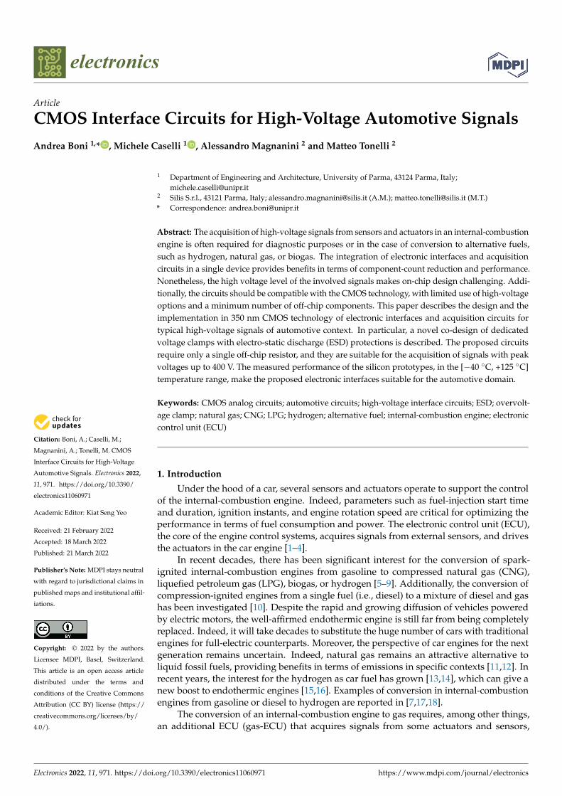
In the internal-combustion engine, the injector is an electro-magnetic valve used to dis-pense fuel either into the intake manifold or directly into the combustion chamber [22–24].The latter case usually guarantees better power performance and lower consumption, and itcorresponds to spark-ignition engines with gasoline direct injection (GDI) or diesel engineswith common-rail direct injection (CRDI). A typical driving circuit for the fuel injectors inGDI or CRDI engines is shown in Figure 1a. The power-MOS transistors MH1 and MH2connect the high side of the injector, modeled with an L-R equivalent, to either the batteryvoltage, i.e., 12 V, or to a high-voltage rail, up to approximately 80 V. The latter is locallygenerated by a DC–DC converter, shared among all the injectors [25,26].
Electronics 2022, 11, 971 3 of 18
DC/DC
CMDH1
CMDL
VBAT
VHV
(a)
ML1
MH1MH2
INJ
G-DRIV.
t [ms]
t [ms]
VHS
VLS
OFF PM BS
LSMOD
HSMOD
OFF
(b)
(c)
VBAT
VHV
tA tB tC
MOD OFF
ON
tD
CMDH2
CMDH1
CMDL
t [ms]
(d)
CMDH2
G-DRIV.
VHS
VLS
VBAT = 12 V, VHV 80 V
tC – tB 400 ms, tD – tA 1.5 ms
Figure 1. (a): Dual-voltage driver for fuel-injection device in GDI and common-rail engines. (b): Voltagewaveform at the high-side terminal. (c): voltage waveform at the low-side terminal. (d): commandwaveforms of low and high-side switches (high-level corresponds to the closed-state).
This dual-voltage control increases the time derivative of the current at the onset of theinjector activation with respect to the case of a single 12 V supply, leading to more accuratecontrol of the fuel-injection startup time. The insulated-gate bipolar transistor (IGBT) ML1,connected to the injector low side, is used to rapidly reduce the driving current during theinjection phase and at the end of the injection window. The simplified voltage waveformsat the high and low sides of the injector are shown in Figure 1b,c, respectively, while thecommand waveforms, i.e., CMDL1, CMDH1, and CMDH2, are in Figure 1d, where thehigh-level condition corresponds to the closed-switch state.
In the OFF phase, the low-side switch is open, and the high-side terminal of the injectoris connected to the battery rail. At tA, the preliminary magnetization (PM) phase starts withML1 closed and the current flowing through the injector coil. The fuel injection starts at tB,when the high side is connected to the high-voltage rail and the time derivative of the inputcurrent suddenly increases, achieving a fast injector activation. Once the injector has beencompletely switched on, the bootstrap (BS) phase ends and the control current is reducedto limit the thermal stress of the coil. Thus, the modulation (MOD) phase occurs from tconwards, with the injector initially disconnected from the high-voltage rail by switchingoff the high-side transistor. The injector modulation is implemented also at the low-side(LSMOD) by switching off ML1 for a short time. This procedure rapidly decreases thecurrent to the minimum level, but still maintains the injector in the ON state. Moreover,it causes the low-side voltage to abruptly rise to the clamping voltage, usually set by theprotection diode of ML1, not included in the figure. For the remaining time of the injectionwindow, the high side is periodically connected to the battery rail to maintain the injectorcurrent at the required level, i.e., high-side modulation (HSMOD) [27]. The injection phaseterminates at tD by switching off the low-side device, causing the low-side voltage to riseagain to the clamping voltage, which is typically in the 80–100 V range.
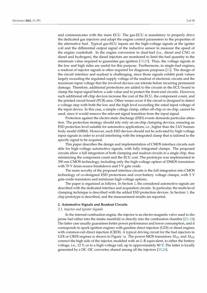
For diagnostic or control purposes the length of the high-voltage pulse at the high-side,i.e., tC − tB, matters. Additionally, the functionality of the low-side switch is monitored bydetecting the crossing of a threshold set at half the battery voltage measuring tA, tC, and tD.An example of measured voltage waveform at the injector high side in a GDI engine is inthe plot of Figure 2a.
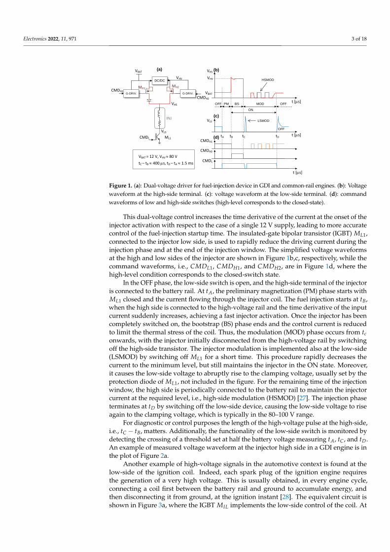
Another example of high-voltage signals in the automotive context is found at thelow-side of the ignition coil. Indeed, each spark plug of the ignition engine requiresthe generation of a very high voltage. This is usually obtained, in every engine cycle,connecting a coil first between the battery rail and ground to accumulate energy, andthen disconnecting it from ground, at the ignition instant [28]. The equivalent circuit isshown in Figure 3a, where the IGBT MIL implements the low-side control of the coil. At
Electronics 2022, 11, 971 4 of 18
the low-to-high transition, the voltage at the IGBT collector increases up to about 400 Vto successively settle to the battery voltage level [29,30]. The ignition instant, i.e., t2 inFigure 3b, is precisely measured by detecting the crossing of the low-side coil voltageat a threshold, usually set to half the car-battery voltage, VBAT/2. It should be noticedthat the coil inductance combined with the capacitance at the IGBT collector can lead to anegative voltage transient at the beginning of the coil pre-charge phase, i.e., t1, with theIGBT switched on. A measured waveform at the low side of the ignition coil is shown inFigure 2b.
0 0.5 1 1.5 2
time [ms]
0
20
40
60
80
VH
S [V
]
0 10 20 30 40 50
time [ s]
0
200
400
VC
OIL
[V
]
(b)
(a)
Figure 2. (a): Measured voltage waveform at the high-side of a GDI-engine injector. (b): Measuredvoltage waveform at the input of the ignition coil.
CMDIG
VBAT
t [ms]
VPKIG
VBAT
VON
(a) (b)
t1 t2
VPKN
coil
MIL
Figure 3. (a): IGBT-based driving circuit for ignition coil. (b): voltage waveform at the low-sideterminal of the coil.
2.2. Integrated Interface Circuit with Multi-Level Voltage Clamping
Sensing the voltage signal at the injector pins or at the low side of the ignition coil raisesnon-trivial design issues. In the case of the injector low side, the circuit must detect both therising and falling crossing of a reference voltage usually set at VBAT/2. Regarding the ignitercoil signal, the reference crossing in the low–high transition is relevant information to assessthe ignition time instant. In both cases, the interface circuit should withstand repetitivepulses as high as 100 V and 400 V for the fuel injector and the ignition coil, respectively.
This overvoltage condition is particularly critical for the ESD clamping circuit con-nected to the pad. An ESD protection circuit can be implemented either with a pair ofdiodes connecting the input pin to the ground and supply rail [31] or with a bidirectionalclamp connecting the pad to the ground rail. The former solution is not suitable for protect-
Electronics 2022, 11, 971 5 of 18
ing the interface circuits in automotive applications, where over-battery conditions oftenoccur, as in the case of igniter or injector signals. Indeed, the diode connected to the supplyrail would be forward-biased in such a case. Furthermore, the input signal may be presentalso when the device is disconnected from the 5 V regulated supply.
In CMOS technologies, bidirectional clamps to ground are often based on gate-grounded NMOS (GGNMOS) [32,33], gate-coupling NMOS (GCNMOS) [34], or RC-triggeredNMOS [35,36]. The voltage at the protected pad is limited either by the breakdown or thesnap-back activation of the ESD clamp. The dominant clamping mechanism depends onthe time derivative of the input signal, with the snap-back promoted by a fast variation ofthe input voltage.
The direct sizing of an ESD protection for a breakdown voltage higher than the peakvalue of the ignition coil or injector signals is not feasible. Indeed, considering a GGNMOSas a clamp device, its drain-to-substrate breakdown voltage must be higher than 400 V. Thisdevice is seldom available in high-voltage CMOS technologies with DMOS transistors witha typical breakdown voltage within 100 V [37]. Additionally, a high breakdown voltagecould be obtained by stacking several GGNMOS devices [38,39], but with a significantsilicon area penalty. Indeed, the width of each transistor correlates with the number ofstacked devices to keep the overall series resistance of the discharge suitable for the targetESD protection level.
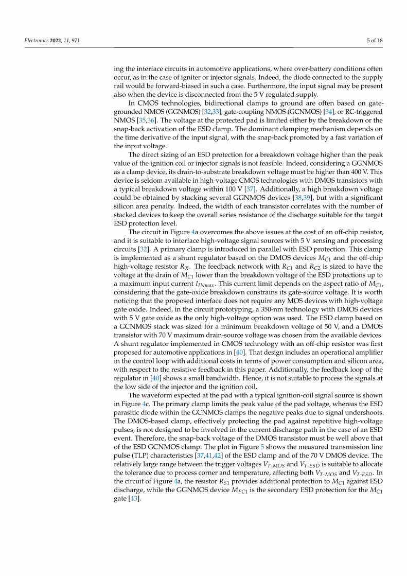
The circuit in Figure 4a overcomes the above issues at the cost of an off-chip resistor,and it is suitable to interface high-voltage signal sources with 5 V sensing and processingcircuits [32]. A primary clamp is introduced in parallel with ESD protection. This clampis implemented as a shunt regulator based on the DMOS devices MC1 and the off-chiphigh-voltage resistor RX. The feedback network with RC1 and RC2 is sized to have thevoltage at the drain of MC1 lower than the breakdown voltage of the ESD protections up toa maximum input current IINmax. This current limit depends on the aspect ratio of MC1,considering that the gate-oxide breakdown constrains its gate-source voltage. It is worthnoticing that the proposed interface does not require any MOS devices with high-voltagegate oxide. Indeed, in the circuit prototyping, a 350-nm technology with DMOS deviceswith 5 V gate oxide as the only high-voltage option was used. The ESD clamp based ona GCNMOS stack was sized for a minimum breakdown voltage of 50 V, and a DMOStransistor with 70 V maximum drain-source voltage was chosen from the available devices.A shunt regulator implemented in CMOS technology with an off-chip resistor was firstproposed for automotive applications in [40]. That design includes an operational amplifierin the control loop with additional costs in terms of power consumption and silicon area,with respect to the resistive feedback in this paper. Additionally, the feedback loop of theregulator in [40] shows a small bandwidth. Hence, it is not suitable to process the signals atthe low side of the injector and the ignition coil.
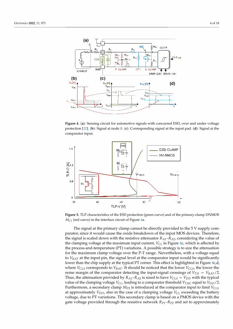
The waveform expected at the pad with a typical ignition-coil signal source is shownin Figure 4c. The primary clamp limits the peak value of the pad voltage, whereas the ESDparasitic diode within the GCNMOS clamps the negative peaks due to signal undershoots.The DMOS-based clamp, effectively protecting the pad against repetitive high-voltagepulses, is not designed to be involved in the current discharge path in the case of an ESDevent. Therefore, the snap-back voltage of the DMOS transistor must be well above thatof the ESD GCNMOS clamp. The plot in Figure 5 shows the measured transmission linepulse (TLP) characteristics [37,41,42] of the ESD clamp and of the 70 V DMOS device. Therelatively large range between the trigger voltages VT-MOS and VT-ESD is suitable to allocatethe tolerance due to process corner and temperature, affecting both VT-MOS and VT-ESD. Inthe circuit of Figure 4a, the resistor RS1 provides additional protection to MC1 against ESDdischarge, while the GGNMOS device MPC1 is the secondary ESD protection for the MC1gate [43].
Electronics 2022, 11, 971 6 of 18
Figure 4. (a): Sensing circuit for automotive signals with concurred ESD, over and under voltageprotection [32]. (b): Signal at node S. (c): Corresponding signal at the input pad. (d): Signal at thecomparator input.
Figure 5. TLP characteristics of the ESD protection (green curve) and of the primary-clamp DNMOSMC1 (red curve) in the interface circuit of Figure 4a.
The signal at the primary clamp cannot be directly provided to the 5 V supply com-parator, since it would cause the oxide breakdown of the input MOS devices. Therefore,the signal is scaled down with the resistive attenuator RA1–RA2, considering the value ofthe clamping voltage at the maximum input current, VCL in Figure 4c, which is affected bythe process-and-temperature (PT) variations. A possible strategy is to size the attenuationfor the maximum clamp voltage over the P-T range. Nevertheless, with a voltage equalto VBAT at the input pin, the signal level at the comparator input would be significantlylower than the chip supply at the typical PT corner. This effect is highlighted in Figure 4c,d,where VCLS corresponds to VBAT . It should be noticed that the lower VCLS, the lower thenoise margin of the comparator detecting the input-signal crossings of VTH = VBAT/2.Thus, the attenuation provided by RA1–RA2 is sized to have VCLS = VDD with the typicalvalue of the clamping voltage VCL, leading to a comparator threshold VTHC equal to VDD/2.Furthermore, a secondary clamp MP2 is introduced at the comparator input to limit VCLSat approximately VDD, also in the case of a clamping voltage VCL exceeding the batteryvoltage, due to PT variations. This secondary clamp is based on a PMOS device with thegate voltage provided through the resistive network RP1–RP2 and set to approximately
Electronics 2022, 11, 971 7 of 18
VDD + VTP, with VTP corresponding to the threshold voltage of MP2. The final waveformat the comparator input is shown in Figure 4d. It is worth noticing that this combination oftwo clamping circuits and signal attenuator properly protects both the ESD clamps and thecomparator against the repetitive 100 V signal peaks, without affecting the detection of thethreshold crossings.
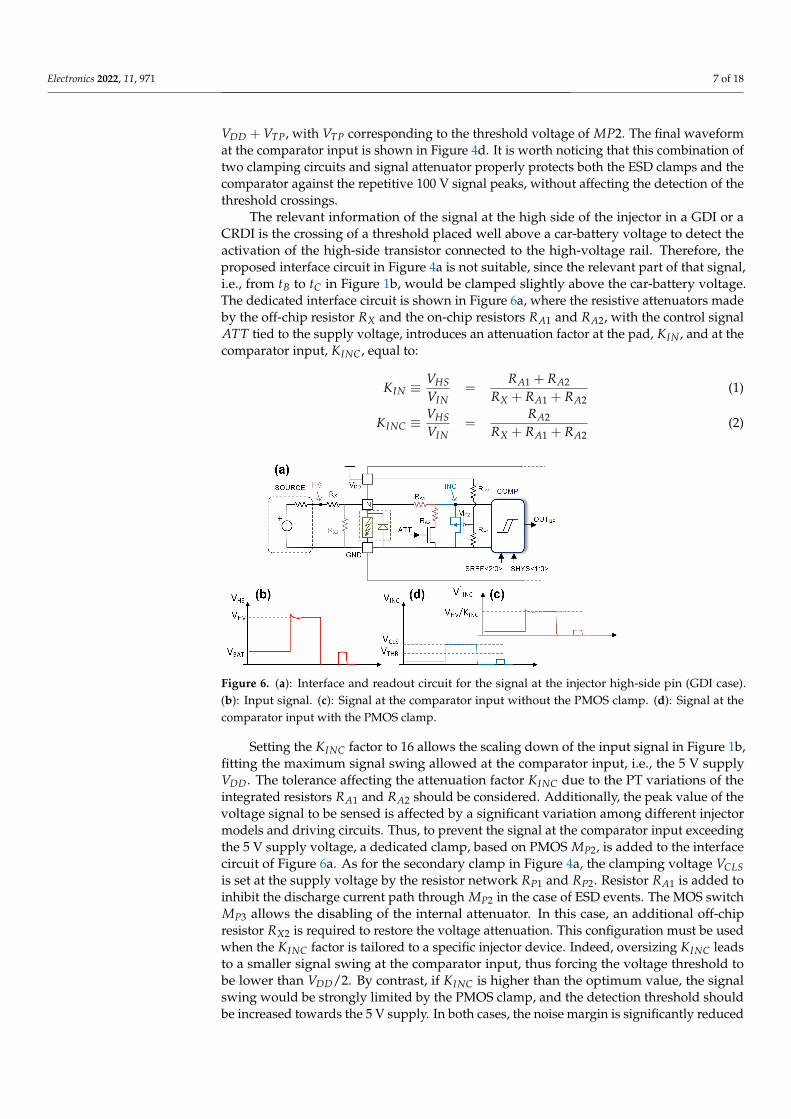
The relevant information of the signal at the high side of the injector in a GDI or aCRDI is the crossing of a threshold placed well above a car-battery voltage to detect theactivation of the high-side transistor connected to the high-voltage rail. Therefore, theproposed interface circuit in Figure 4a is not suitable, since the relevant part of that signal,i.e., from tB to tC in Figure 1b, would be clamped slightly above the car-battery voltage.The dedicated interface circuit is shown in Figure 6a, where the resistive attenuators madeby the off-chip resistor RX and the on-chip resistors RA1 and RA2, with the control signalATT tied to the supply voltage, introduces an attenuation factor at the pad, KIN , and at thecomparator input, KINC, equal to:
KIN ≡ VHSVIN
=RA1 + RA2
RX + RA1 + RA2(1)
KINC ≡ VHSVIN
=RA2
RX + RA1 + RA2(2)
Figure 6. (a): Interface and readout circuit for the signal at the injector high-side pin (GDI case).(b): Input signal. (c): Signal at the comparator input without the PMOS clamp. (d): Signal at thecomparator input with the PMOS clamp.
Setting the KINC factor to 16 allows the scaling down of the input signal in Figure 1b,fitting the maximum signal swing allowed at the comparator input, i.e., the 5 V supplyVDD. The tolerance affecting the attenuation factor KINC due to the PT variations of theintegrated resistors RA1 and RA2 should be considered. Additionally, the peak value of thevoltage signal to be sensed is affected by a significant variation among different injectormodels and driving circuits. Thus, to prevent the signal at the comparator input exceedingthe 5 V supply voltage, a dedicated clamp, based on PMOS MP2, is added to the interfacecircuit of Figure 6a. As for the secondary clamp in Figure 4a, the clamping voltage VCLSis set at the supply voltage by the resistor network RP1 and RP2. Resistor RA1 is added toinhibit the discharge current path through MP2 in the case of ESD events. The MOS switchMP3 allows the disabling of the internal attenuator. In this case, an additional off-chipresistor RX2 is required to restore the voltage attenuation. This configuration must be usedwhen the KINC factor is tailored to a specific injector device. Indeed, oversizing KINC leadsto a smaller signal swing at the comparator input, thus forcing the voltage threshold tobe lower than VDD/2. By contrast, if KINC is higher than the optimum value, the signalswing would be strongly limited by the PMOS clamp, and the detection threshold shouldbe increased towards the 5 V supply. In both cases, the noise margin is significantly reduced
Electronics 2022, 11, 971 8 of 18
with respect to the optimum attenuation factor, leading to a detection threshold equalto VDD/2.
2.3. Inductive Phonic-Wheel Sensor
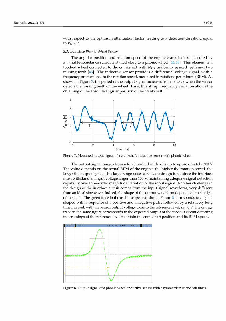
The angular position and rotation speed of the engine crankshaft is measured bya variable-reluctance sensor installed close to a phonic wheel [44,45]. This element is atoothed wheel connected to the crankshaft with NTH uniformly spaced teeth and twomissing teeth [46]. The inductive sensor provides a differential voltage signal, with afrequency proportional to the rotation speed, measured in rotations per minute (RPM). Asshown in Figure 7, the period of the output signal increases from T1 to T2 when the sensordetects the missing teeth on the wheel. Thus, this abrupt frequency variation allows theobtaining of the absolute angular position of the crankshaft.
0 2 4 6 8 10
time [ms]
-4
-2
0
2
4
6
VP
hW
[V
]
T2
T1
Figure 7. Measured output signal of a crankshaft inductive sensor with phonic wheel.
The output signal ranges from a few hundred millivolts up to approximately 200 V.The value depends on the actual RPM of the engine: the higher the rotation speed, thelarger the output signal. This large range raises a relevant design issue since the interfacemust withstand an input voltage larger than 100 V, maintaining adequate signal detectioncapability over three-order magnitude variation of the input signal. Another challenge inthe design of the interface circuit comes from the input-signal waveform, very differentfrom an ideal sine wave. Indeed, the shape of the output waveform depends on the designof the teeth. The green trace in the oscilloscope snapshot in Figure 8 corresponds to a signalshaped with a sequence of a positive and a negative pulse followed by a relatively longtime interval, with the sensor output voltage close to the reference level, i.e., 0 V. The orangetrace in the same figure corresponds to the expected output of the readout circuit detectingthe crossings of the reference level to obtain the crankshaft position and its RPM speed.
Figure 8. Output signal of a phonic-wheel inductive sensor with asymmetric rise and fall times.
Electronics 2022, 11, 971 9 of 18
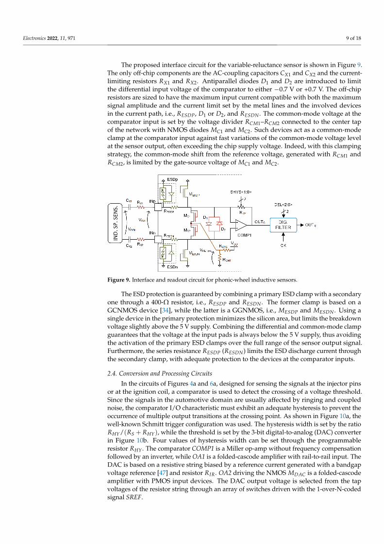
The proposed interface circuit for the variable-reluctance sensor is shown in Figure 9.The only off-chip components are the AC-coupling capacitors CX1 and CX2 and the current-limiting resistors RX1 and RX2. Antiparallel diodes D1 and D2 are introduced to limitthe differential input voltage of the comparator to either −0.7 V or +0.7 V. The off-chipresistors are sized to have the maximum input current compatible with both the maximumsignal amplitude and the current limit set by the metal lines and the involved devicesin the current path, i.e., RESDP, D1 or D2, and RESDN . The common-mode voltage at thecomparator input is set by the voltage divider RCM1–RCM2 connected to the center tapof the network with NMOS diodes MC1 and MC2. Such devices act as a common-modeclamp at the comparator input against fast variations of the common-mode voltage levelat the sensor output, often exceeding the chip supply voltage. Indeed, with this clampingstrategy, the common-mode shift from the reference voltage, generated with RCM1 andRCM2, is limited by the gate-source voltage of MC1 and MC2.
Figure 9. Interface and readout circuit for phonic-wheel inductive sensors.
The ESD protection is guaranteed by combining a primary ESD clamp with a secondaryone through a 400-Ω resistor, i.e., RESDP and RESDN . The former clamp is based on aGCNMOS device [34], while the latter is a GGNMOS, i.e., MESDP and MESDN . Using asingle device in the primary protection minimizes the silicon area, but limits the breakdownvoltage slightly above the 5 V supply. Combining the differential and common-mode clampguarantees that the voltage at the input pads is always below the 5 V supply, thus avoidingthe activation of the primary ESD clamps over the full range of the sensor output signal.Furthermore, the series resistance RESDP (RESDN) limits the ESD discharge current throughthe secondary clamp, with adequate protection to the devices at the comparator inputs.
2.4. Conversion and Processing Circuits
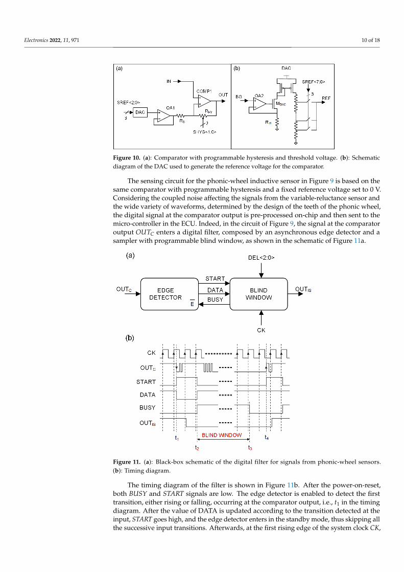
In the circuits of Figures 4a and 6a, designed for sensing the signals at the injector pinsor at the ignition coil, a comparator is used to detect the crossing of a voltage threshold.Since the signals in the automotive domain are usually affected by ringing and couplednoise, the comparator I/O characteristic must exhibit an adequate hysteresis to prevent theoccurrence of multiple output transitions at the crossing point. As shown in Figure 10a, thewell-known Schmitt trigger configuration was used. The hysteresis width is set by the ratioRHY/(RS + RHY), while the threshold is set by the 3-bit digital-to-analog (DAC) converterin Figure 10b. Four values of hysteresis width can be set through the programmableresistor RHY. The comparator COMP1 is a Miller op-amp without frequency compensationfollowed by an inverter, while OA1 is a folded-cascode amplifier with rail-to-rail input. TheDAC is based on a resistive string biased by a reference current generated with a bandgapvoltage reference [47] and resistor RIR. OA2 driving the NMOS MDAC is a folded-cascodeamplifier with PMOS input devices. The DAC output voltage is selected from the tapvoltages of the resistor string through an array of switches driven with the 1-over-N-codedsignal SREF.
Electronics 2022, 11, 971 10 of 18
Figure 10. (a): Comparator with programmable hysteresis and threshold voltage. (b): Schematicdiagram of the DAC used to generate the reference voltage for the comparator.
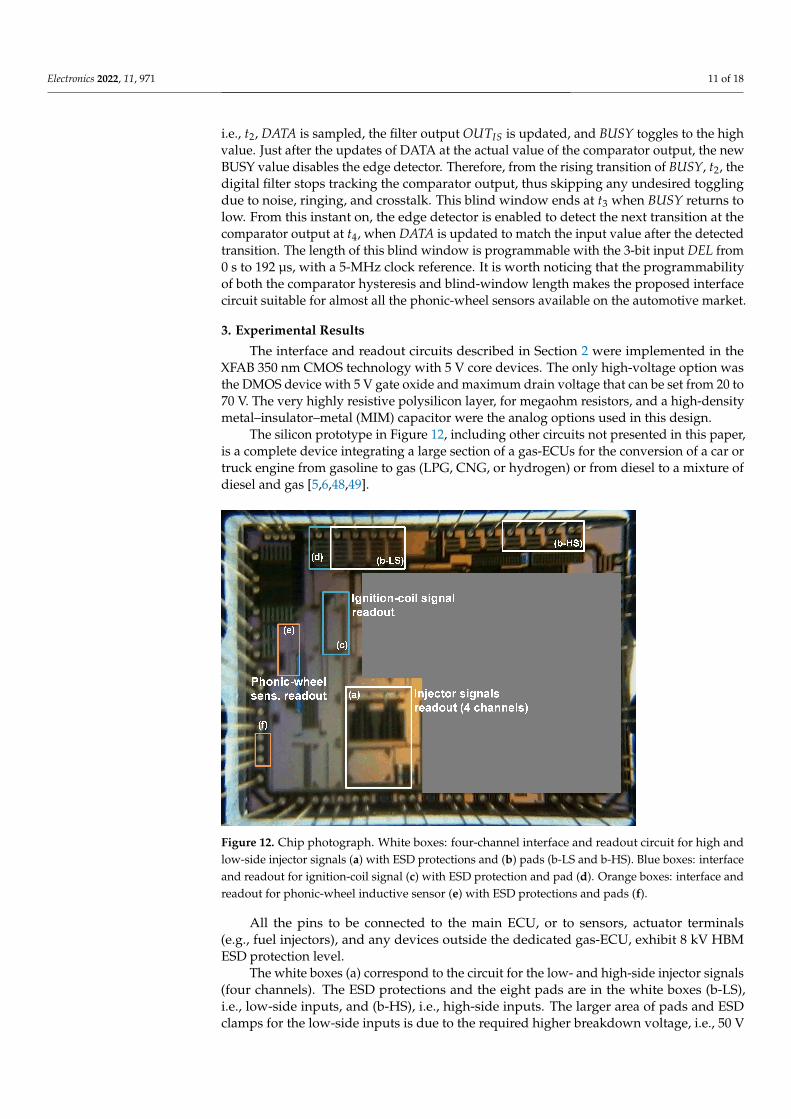
The sensing circuit for the phonic-wheel inductive sensor in Figure 9 is based on thesame comparator with programmable hysteresis and a fixed reference voltage set to 0 V.Considering the coupled noise affecting the signals from the variable-reluctance sensor andthe wide variety of waveforms, determined by the design of the teeth of the phonic wheel,the digital signal at the comparator output is pre-processed on-chip and then sent to themicro-controller in the ECU. Indeed, in the circuit of Figure 9, the signal at the comparatoroutput OUTC enters a digital filter, composed by an asynchronous edge detector and asampler with programmable blind window, as shown in the schematic of Figure 11a.
Figure 11. (a): Black-box schematic of the digital filter for signals from phonic-wheel sensors.(b): Timing diagram.
The timing diagram of the filter is shown in Figure 11b. After the power-on-reset,both BUSY and START signals are low. The edge detector is enabled to detect the firsttransition, either rising or falling, occurring at the comparator output, i.e., t1 in the timingdiagram. After the value of DATA is updated according to the transition detected at theinput, START goes high, and the edge detector enters in the standby mode, thus skipping allthe successive input transitions. Afterwards, at the first rising edge of the system clock CK,
Electronics 2022, 11, 971 11 of 18
i.e., t2, DATA is sampled, the filter output OUTIS is updated, and BUSY toggles to the highvalue. Just after the updates of DATA at the actual value of the comparator output, the newBUSY value disables the edge detector. Therefore, from the rising transition of BUSY, t2, thedigital filter stops tracking the comparator output, thus skipping any undesired togglingdue to noise, ringing, and crosstalk. This blind window ends at t3 when BUSY returns tolow. From this instant on, the edge detector is enabled to detect the next transition at thecomparator output at t4, when DATA is updated to match the input value after the detectedtransition. The length of this blind window is programmable with the 3-bit input DEL from0 s to 192 µs, with a 5-MHz clock reference. It is worth noticing that the programmabilityof both the comparator hysteresis and blind-window length makes the proposed interfacecircuit suitable for almost all the phonic-wheel sensors available on the automotive market.
3. Experimental Results
The interface and readout circuits described in Section 2 were implemented in theXFAB 350 nm CMOS technology with 5 V core devices. The only high-voltage option wasthe DMOS device with 5 V gate oxide and maximum drain voltage that can be set from 20 to70 V. The very highly resistive polysilicon layer, for megaohm resistors, and a high-densitymetal–insulator–metal (MIM) capacitor were the analog options used in this design.
The silicon prototype in Figure 12, including other circuits not presented in this paper,is a complete device integrating a large section of a gas-ECUs for the conversion of a car ortruck engine from gasoline to gas (LPG, CNG, or hydrogen) or from diesel to a mixture ofdiesel and gas [5,6,48,49].
Figure 12. Chip photograph. White boxes: four-channel interface and readout circuit for high andlow-side injector signals (a) with ESD protections and (b) pads (b-LS and b-HS). Blue boxes: interfaceand readout for ignition-coil signal (c) with ESD protection and pad (d). Orange boxes: interface andreadout for phonic-wheel inductive sensor (e) with ESD protections and pads (f).
All the pins to be connected to the main ECU, or to sensors, actuator terminals(e.g., fuel injectors), and any devices outside the dedicated gas-ECU, exhibit 8 kV HBMESD protection level.
The white boxes (a) correspond to the circuit for the low- and high-side injector signals(four channels). The ESD protections and the eight pads are in the white boxes (b-LS),i.e., low-side inputs, and (b-HS), i.e., high-side inputs. The larger area of pads and ESDclamps for the low-side inputs is due to the required higher breakdown voltage, i.e., 50 V
Electronics 2022, 11, 971 12 of 18
against 30 V for the high-side inputs. The readout circuits for the ignition-coil signal are inthe blue box (c) with the ESD clamp (50 V breakdown) and pad in box (d). Orange boxes(e) and (f) refer to the readout circuit and 5 V pad with ESD clamp for the phonic-wheelinductive sensor.
The plots in Figure 13 show the measured voltage at the input pin of the interfacecircuit for the ignition-coil or the low-side injector signal. Since the metal input line andthe drain contacts of MC1 in Figure 4a are sized for a maximum current of 2 mA, fromthe measurement results in Figure 13a, a maximum source voltage VS as high as 400 V istolerated by the interface circuit without any damage, or a significant shift of the inputleakage current. In the case of a negative source signal, the drain-to-substrate diode ofthe GC-NMOS devices in the ESD clamp, i.e., MN to M1 in Figure 5, is forward-biased.Considering the large diode area, a current of 100 µA can be tolerated without affecting theESD devices. Therefore, with a 220-kΩ series resistor, a negative source voltage lower than−10 V can be tolerated by the interface circuits.
10-6
10-4
10-2
100
Iin
[mA]
0
10
20
30
VP
AD
[V
]
-40 °C
27 °C
125 °C
-0.1 -0.08 -0.06 -0.04 -0.02 0
Iin
[mA]
-0.8
-0.6
-0.4
-0.2
VP
AD
[V
]
(a)
(b)
Figure 13. Voltage at the input of the interface circuit with multi-level voltage clamps in Figure 4vs. input current, at −40 C, 27 C, and 125 C chip temperature. (a) Positive input current sweep;(b) Negative input current sweep.
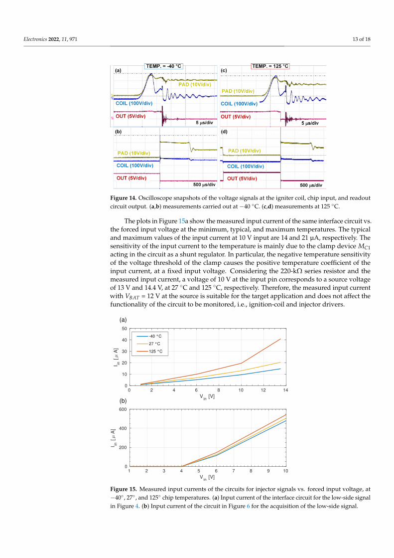
The circuit in Figure 4a was tested in a dedicated ECU, interfaced to the low- andhigh-side pins of the injector, to the ignition coil, and the phonic-wheel sensors of a GDIengine. The oscilloscope snapshots in Figure 14 shows the signal at the ignition coil (bluetrace), with a peak value of approximately 350 V, and the signal at the input pin, properlylimited below 30 V (yellow trace) by the proposed clamp. The input and output signalswere acquired at the minimum and maximum temperatures of the automotive range, i.e.,−40 and 125. For these measurements, the device with the test-board was placed in aclimatic chamber and the input signal was provided by an emulator of automotive signals(located outside the chamber).
Electronics 2022, 11, 971 13 of 18
Figure 14. Oscilloscope snapshots of the voltage signals at the igniter coil, chip input, and readoutcircuit output. (a,b) measurements carried out at −40 C. (c,d) measurements at 125 C.
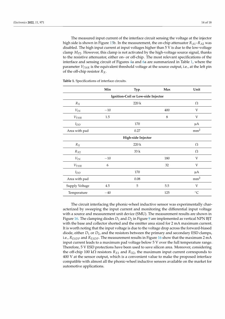
The plots in Figure 15a show the measured input current of the same interface circuit vs.the forced input voltage at the minimum, typical, and maximum temperatures. The typicaland maximum values of the input current at 10 V input are 14 and 21 µA, respectively. Thesensitivity of the input current to the temperature is mainly due to the clamp device MC1acting in the circuit as a shunt regulator. In particular, the negative temperature sensitivityof the voltage threshold of the clamp causes the positive temperature coefficient of theinput current, at a fixed input voltage. Considering the 220-kΩ series resistor and themeasured input current, a voltage of 10 V at the input pin corresponds to a source voltageof 13 V and 14.4 V, at 27 C and 125 C, respectively. Therefore, the measured input currentwith VBAT = 12 V at the source is suitable for the target application and does not affect thefunctionality of the circuit to be monitored, i.e., ignition-coil and injector drivers.
0 2 4 6 8 10 12 14
Vin
[V]
0
10
20
30
40
50
I in [
A]
-40 °C
27 °C
125 °C
1 2 3 4 5 6 7 8 9 10
Vin
[V]
0
200
400
600
I in [
A]
(a)
(b)
Figure 15. Measured input currents of the circuits for injector signals vs. forced input voltage, at−40, 27, and 125 chip temperatures. (a) Input current of the interface circuit for the low-side signalin Figure 4. (b) Input current of the circuit in Figure 6 for the acquisition of the low-side signal.
Electronics 2022, 11, 971 14 of 18
The measured input current of the interface circuit sensing the voltage at the injectorhigh side is shown in Figure 15b. In the measurement, the on-chip attenuator RA1–RA2 wasdisabled. The high input current at input voltages higher than 5 V is due to the low-voltageclamp MP2. However, this clamp is not activated by the high-voltage source signal, thanksto the resistive attenuator, either on- or off-chip. The most relevant specifications of theinterface and sensing circuit of Figures 4a and 6a are summarized in Table 1, where theparameter VTHR is the equivalent threshold voltage at the source output, i.e., at the left pinof the off-chip resistor RX .
Table 1. Specifications of interface circuits.
Min Typ. Max Unit
Ignition-Coil or Low-side Injector
RX 220 k Ω
VIN −10 400 V
VTHR 1.5 8 V
IDD 170 µA
Area with pad 0.27 mm2
High-side Injector
RX 220 k Ω
RX2 33 k Ω
VIN −10 180 V
VTHR 6 32 V
IDD 170 µA
Area with pad 0.08 mm2
Supply Voltage 4.5 5 5.5 V
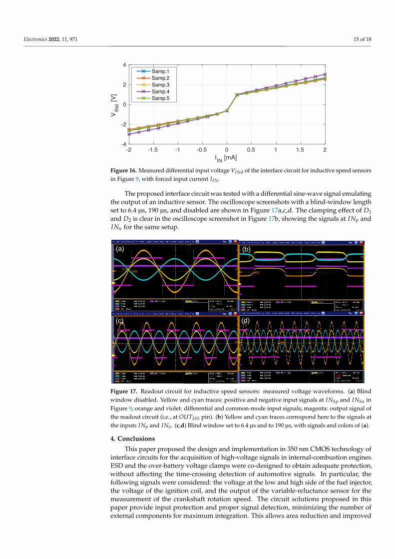
Temperature −40 125 C
The circuit interfacing the phonic-wheel inductive sensor was experimentally char-acterized by sweeping the input current and monitoring the differential input voltagewith a source and measurement unit device (SMU). The measurement results are shown inFigure 16. The clamping diodes D1 and D2 in Figure 9 are implemented as vertical NPN BJTwith the base and collector shorted and the emitter area sized for 2 mA maximum current.It is worth noting that the input voltage is due to the voltage drop across the forward-biaseddiode, either D1 or D2, and the resistors between the primary and secondary ESD clamps,i.e., RESDP and RESDP. The measurement results in Figure 16 show that the maximum 2 mAinput current leads to a maximum pad voltage below 5 V over the full temperature range.Therefore, 5 V ESD protections have been used to save silicon area. Moreover, consideringthe off-chip 100 kΩ resistors RX1 and RX2, the maximum input current corresponds to400 V at the sensor output, which is a convenient value to make the proposed interfacecompatible with almost all the phonic-wheel inductive sensors available on the market forautomotive applications.
Electronics 2022, 11, 971 15 of 18
-2 -1.5 -1 -0.5 0 0.5 1 1.5 2
IIN
[mA]
-4
-2
0
2
4
VIN
d [V
]
Samp.1
Samp.2
Samp.3
Samp.4
Samp.5
Figure 16. Measured differential input voltage VINd of the interface circuit for inductive speed sensorsin Figure 9, with forced input current IIN .
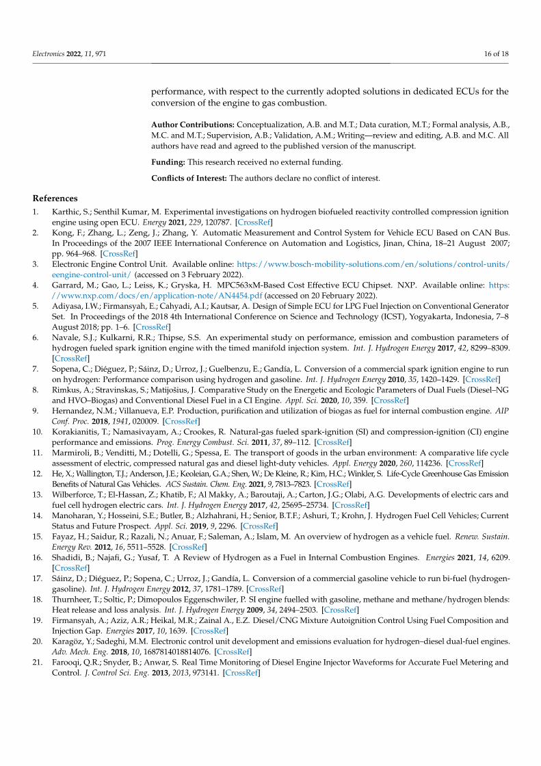
The proposed interface circuit was tested with a differential sine-wave signal emulatingthe output of an inductive sensor. The oscilloscope screenshots with a blind-window lengthset to 6.4 µs, 190 µs, and disabled are shown in Figure 17a,c,d. The clamping effect of D1and D2 is clear in the oscilloscope screenshot in Figure 17b, showing the signals at INp andINn for the same setup.
(d)
(b)(a)
(c)
Figure 17. Readout circuit for inductive speed sensors: measured voltage waveforms. (a) Blindwindow disabled. Yellow and cyan traces: positive and negative input signals at INSp and INSn inFigure 9; orange and violet: differential and common-mode input signals; magenta: output signal ofthe readout circuit (i.e., at OUTISS pin). (b) Yellow and cyan traces correspond here to the signals atthe inputs INp and INn. (c,d) Blind window set to 6.4 µs and to 190 µs, with signals and colors of (a).
4. Conclusions
This paper proposed the design and implementation in 350 nm CMOS technology ofinterface circuits for the acquisition of high-voltage signals in internal-combustion engines.ESD and the over-battery voltage clamps were co-designed to obtain adequate protection,without affecting the time-crossing detection of automotive signals. In particular, thefollowing signals were considered: the voltage at the low and high side of the fuel injector,the voltage of the ignition coil, and the output of the variable-reluctance sensor for themeasurement of the crankshaft rotation speed. The circuit solutions proposed in thispaper provide input protection and proper signal detection, minimizing the number ofexternal components for maximum integration. This allows area reduction and improved
Electronics 2022, 11, 971 16 of 18
performance, with respect to the currently adopted solutions in dedicated ECUs for theconversion of the engine to gas combustion.
Author Contributions: Conceptualization, A.B. and M.T.; Data curation, M.T.; Formal analysis, A.B.,M.C. and M.T.; Supervision, A.B.; Validation, A.M.; Writing—review and editing, A.B. and M.C. Allauthors have read and agreed to the published version of the manuscript.
Funding: This research received no external funding.
Conflicts of Interest: The authors declare no conflict of interest.
References1. Karthic, S.; Senthil Kumar, M. Experimental investigations on hydrogen biofueled reactivity controlled compression ignition
engine using open ECU. Energy 2021, 229, 120787. [CrossRef]2. Kong, F.; Zhang, L.; Zeng, J.; Zhang, Y. Automatic Measurement and Control System for Vehicle ECU Based on CAN Bus.
In Proceedings of the 2007 IEEE International Conference on Automation and Logistics, Jinan, China, 18–21 August 2007;pp. 964–968. [CrossRef]
3. Electronic Engine Control Unit. Available online: https://www.bosch-mobility-solutions.com/en/solutions/control-units/eengine-control-unit/ (accessed on 3 February 2022).
4. Garrard, M.; Gao, L.; Leiss, K.; Gryska, H. MPC563xM-Based Cost Effective ECU Chipset. NXP. Available online: https://www.nxp.com/docs/en/application-note/AN4454.pdf (accessed on 20 February 2022).
5. Adiyasa, I.W.; Firmansyah, E.; Cahyadi, A.I.; Kautsar, A. Design of Simple ECU for LPG Fuel Injection on Conventional GeneratorSet. In Proceedings of the 2018 4th International Conference on Science and Technology (ICST), Yogyakarta, Indonesia, 7–8August 2018; pp. 1–6. [CrossRef]
6. Navale, S.J.; Kulkarni, R.R.; Thipse, S.S. An experimental study on performance, emission and combustion parameters ofhydrogen fueled spark ignition engine with the timed manifold injection system. Int. J. Hydrogen Energy 2017, 42, 8299–8309.[CrossRef]
7. Sopena, C.; Diéguez, P.; Sáinz, D.; Urroz, J.; Guelbenzu, E.; Gandía, L. Conversion of a commercial spark ignition engine to runon hydrogen: Performance comparison using hydrogen and gasoline. Int. J. Hydrogen Energy 2010, 35, 1420–1429. [CrossRef]
8. Rimkus, A.; Stravinskas, S.; Matijošius, J. Comparative Study on the Energetic and Ecologic Parameters of Dual Fuels (Diesel–NGand HVO–Biogas) and Conventional Diesel Fuel in a CI Engine. Appl. Sci. 2020, 10, 359. [CrossRef]
9. Hernandez, N.M.; Villanueva, E.P. Production, purification and utilization of biogas as fuel for internal combustion engine. AIPConf. Proc. 2018, 1941, 020009. [CrossRef]
10. Korakianitis, T.; Namasivayam, A.; Crookes, R. Natural-gas fueled spark-ignition (SI) and compression-ignition (CI) engineperformance and emissions. Prog. Energy Combust. Sci. 2011, 37, 89–112. [CrossRef]
11. Marmiroli, B.; Venditti, M.; Dotelli, G.; Spessa, E. The transport of goods in the urban environment: A comparative life cycleassessment of electric, compressed natural gas and diesel light-duty vehicles. Appl. Energy 2020, 260, 114236. [CrossRef]
12. He, X.; Wallington, T.J.; Anderson, J.E.; Keoleian, G.A.; Shen, W.; De Kleine, R.; Kim, H.C.; Winkler, S. Life-Cycle Greenhouse Gas EmissionBenefits of Natural Gas Vehicles. ACS Sustain. Chem. Eng. 2021, 9, 7813–7823. [CrossRef]
13. Wilberforce, T.; El-Hassan, Z.; Khatib, F.; Al Makky, A.; Baroutaji, A.; Carton, J.G.; Olabi, A.G. Developments of electric cars andfuel cell hydrogen electric cars. Int. J. Hydrogen Energy 2017, 42, 25695–25734. [CrossRef]
14. Manoharan, Y.; Hosseini, S.E.; Butler, B.; Alzhahrani, H.; Senior, B.T.F.; Ashuri, T.; Krohn, J. Hydrogen Fuel Cell Vehicles; CurrentStatus and Future Prospect. Appl. Sci. 2019, 9, 2296. [CrossRef]
15. Fayaz, H.; Saidur, R.; Razali, N.; Anuar, F.; Saleman, A.; Islam, M. An overview of hydrogen as a vehicle fuel. Renew. Sustain.Energy Rev. 2012, 16, 5511–5528. [CrossRef]
16. Shadidi, B.; Najafi, G.; Yusaf, T. A Review of Hydrogen as a Fuel in Internal Combustion Engines. Energies 2021, 14, 6209.[CrossRef]
17. Sáinz, D.; Diéguez, P.; Sopena, C.; Urroz, J.; Gandía, L. Conversion of a commercial gasoline vehicle to run bi-fuel (hydrogen-gasoline). Int. J. Hydrogen Energy 2012, 37, 1781–1789. [CrossRef]
18. Thurnheer, T.; Soltic, P.; Dimopoulos Eggenschwiler, P. SI engine fuelled with gasoline, methane and methane/hydrogen blends:Heat release and loss analysis. Int. J. Hydrogen Energy 2009, 34, 2494–2503. [CrossRef]
19. Firmansyah, A.; Aziz, A.R.; Heikal, M.R.; Zainal A., E.Z. Diesel/CNG Mixture Autoignition Control Using Fuel Composition andInjection Gap. Energies 2017, 10, 1639. [CrossRef]
20. Karagöz, Y.; Sadeghi, M.M. Electronic control unit development and emissions evaluation for hydrogen–diesel dual-fuel engines.Adv. Mech. Eng. 2018, 10, 1687814018814076. [CrossRef]
21. Farooqi, Q.R.; Snyder, B.; Anwar, S. Real Time Monitoring of Diesel Engine Injector Waveforms for Accurate Fuel Metering andControl. J. Control Sci. Eng. 2013, 2013, 973141. [CrossRef]
Electronics 2022, 11, 971 17 of 18
22. Erkus, B.; Sürmen, A.; Ihsan Karamangil, M. A comparative study of carburation and injection fuel supply methods in anLPG-fuelled SI engine. Fuel 2013, 107, 511–517. [CrossRef]
23. Zhang, X.; Palazzolo, A.; Kweon, C.B.; Thomas, E.; Tucker, R.; Kascak, A. Direct Fuel Injector Power Drive System Optimization.SAE Int. J. Engines 2014, 7, 1137–1154. [CrossRef]
24. Tsai, W.C. Optimization of Operating Parameters for Stable and High Operating Performance of a GDI Fuel Injector System.Energies 2020, 13, 2405. [CrossRef]
25. Xiong, J.; Gu, H. An Intelligent Dual-Voltage Driving Method and Circuit For a Common Rail Injector for Heavy-Duty DieselEngines. IEEE Access 2018, 6, 27681–27689. [CrossRef]
26. Kumar, A.; Kumar, A.; Banerjee, N.; Mohan, N.; Ashok, B. Study of the injector drive circuit for a high pressure GDI injector. InProceedings of the 2016 International Conference on Recent Advances and Innovations in Engineering (ICRAIE), Jaipur, India,23–25 December 2016; pp. 1–6. [CrossRef]
27. Visconti, P.; Ventura, V.; Carlucci, A.P.; Strafella, L. Driving electronic board with adjustable piloting signal parameters forcharacterization of Common Rail diesel injectors with pure biodiesel. In Proceedings of the 2016 IEEE 16th InternationalConference on Environment and Electrical Engineering (EEEIC), Florence, Italy, 7–10 June 2016; pp. 1–6. [CrossRef]
28. Tang, Q.; Wojslawowicz, J.; Hoenes, H.P. AN-8208 Introduction to Automotive Ignition Systems. Fairchild Semiconductor Corpo-ration. 2014. Available online: https://www.onsemi.com/pub/Collateral/AN-8208CN.pdf (accessed on 20 February 2022).
29. Kubis, M.; Sebok, M.; Beno, P.; Kucera, M.; Gutten, M. Diagnostics of the ignition system for various fault conditions. InProceedings of the 2020 International Conference on Diagnostics in Electrical Engineering (Diagnostika), Pilsen, Czech Republic,1–4 September 2020; pp. 1–4. [CrossRef]
30. Melina, O.M. Application Note Car Ignition with IGBTs. STMicroelectronics. 1999. Available online: https://www.st.com/resource/en/application_note/an484-car-ignition-with-igbts-stmicroelectronics.pdf (accessed on 20 February 2022).
31. Ker, M.D. Whole-chip ESD protection design with efficient VDD-to-VSS ESD clamp circuits for submicron CMOS VLSI. IEEETrans. Electron Devices 1999, 46, 173–183. [CrossRef]
32. Boni, A.; Tonelli, M.; Magnanini, A.; Caselli, M. Fully integrated CMOS overvoltage protection circuit for automotive applications.Electron. Lett. 2015, 51, 1316–1318. [CrossRef]
33. Zeng, J.; Dong, S.; Liou, J.J.; Han, Y.; Zhong, L.; Wang, W. Design and Analysis of an Area-Efficient High Holding Voltage ESDProtection Device. IEEE Trans. Electron Devices 2015, 62, 606–614. [CrossRef]
34. Wang, Y.; Jia, S.; Chen, Z.; Zhang, G.; Ji, L. A design model of gate-coupling NMOS ESD protection circuit. In Proceedings of the7th International Conference on Solid-State and Integrated Circuits Technology, Beijing, China, 18–21 October 2004; Volume 2,pp. 856–859. [CrossRef]
35. Huang, S.C.; Liao, H.F.; Weng, S.P.; Nidhi, K.; Wang, Y.K.; Chen, Y.J.; Chiou, H.C.; Jou, Y.N.; Lee, J.H.; Liao, C.C. AnalyzingGate-Driven Circuit Parameters for Adding ESD Performances. In Proceedings of the 2019 IEEE International Conference onConsumer Electronics-Taiwan (ICCE-TW), Ilan, Taiwan, 20–22 May 2019; pp. 1–2. [CrossRef]
36. Stockinger, M.; Mertens, R. RC-triggered ESD clamp with low turn-on voltage. In Proceedings of the 2017 IEEE Custom IntegratedCircuits Conference (CICC), Austin, TX, USA, 30 April–3 May 2017; pp. 1–4. [CrossRef]
37. Fan, S.K.; Chen, S.L.; Lin, P.L.; Chen, H.W. Layout Strengthening the ESD Performance for High-Voltage N-Channel LateralDiffused MOSFETs. Electronics 2020, 9, 718. [CrossRef]
38. Worley, E. Stacked ESD Protection Circuit Having Reduced Trigger Voltage. U.S. Patent 2008/0259511 A1, 28 September 2008.39. Thijs, S.; Scholz, M.; Linten, D.; Griffoni, A.; Russ, C.; Stadler, W.; Lafonteese, D.; Vashchenko, V.; Sawada, M.; Concannon,
A.; et al. SCCF—System to component level correlation factor. In Proceedings of the Electrical Overstress/Electrostatic DischargeSymposium Proceedings, Reno, NV, USA, 3–8 October 2010; pp. 1–10.
40. Martins, M.; Dias, J. CMOS Shunt Regulator with Bandgap Reference for Automotive Environment. IEE Proc. Circuits DevicesSyst. 1994, 141, 157–161. [CrossRef]
41. Smedes, T.; Velghe, R.; Ruth, R.; Huitsing, A. The application of Transmission Line Pulse testing for the ESD analysis ofintegrated circuits. In Proceedings of the 2001 Electrical Overstress/Electrostatic Discharge Symposium, Portland, OR, USA,11–13 September 2001; pp. 421–429.
42. Mergens, M.; Wilkening, W.; Mettler, S.; Wolf, H.; Stricker, A.; Fichtner, W. Analysis of lateral DMOS power devices under ESDstress conditions. IEEE Trans. Electron Devices 2000, 47, 2128–2137. [CrossRef]
43. Vashchenko, V.; Scholz, M. System Level ESD Protection; Springer: Cham, Switzerland, 2014. [CrossRef]44. Coppo, F.; Pepe, G.; Roveri, N.; Carcaterra, A. A Multisensing Setup for the Intelligent Tire Monitoring. Sensors 2017, 17, 576.
[CrossRef]45. de Oliveira, A.; Moreira dos Santos, E.C.; Botelho, G.C.; Valente, O.S.; Sodré, J.R. Hydrogen electronic injection system for a diesel
power generator. Int. J. Hydrogen Energy 2013, 38, 7986–7993. [CrossRef]46. Laganá, A.A.; Lima, L.L.; Justo, J.F.; Arruda, B.A.; Santos, M.M. Identification of combustion and detonation in spark ignition
engines using ion current signal. Fuel 2018, 227, 469–477. [CrossRef]47. Caselli, M.; van Liempd, C.; Boni, A.; Stanzione, S. A low-power native NMOS-based bandgap reference operating from −55 C
to 125 C with Li-Ion battery compatibility. Int. J. Circuit Theory Appl. 2021, 49, 1327–1346. [CrossRef]
https://www.st.com/resource/en/application_note/an484-car-ignition-with-igbts-stmicroelectronics.pdf

Electronics 2022, 11, 971 18 of 18
48. Shanmugam, R.M.; Kankariya, N.M.; Honvault, J.; Srinivasan, L.; Viswanatha, H.C.; Nicolas, P.; Saravanan, N.; Christian, D.Performance and Emission Characterization of 1.2 L MPI Engine with Multiple Fuels (E10, LPG and CNG). SAE Int. J. Fuels Lubr.2010, 3, 334–352. [CrossRef]
49. Stepanenko, D.; Kneba, Z. ECU calibration for gaseous dual fuel supply system in compression ignition engines. Combust.Engines 2020, 182, 33–37. [CrossRef]
Related Documents