www.cypress.com Document No. 001-32200 Rev. *F 1 AN32200 PSoC ® 1 - Clocks and Global Resources Author: Ben Kropf and M. Ganesh Raja Associated Project: No Associated Part Family: CY7C64215, CY8C21x23, CY8C21x34, CY8C24x23A, CY8C24x94, CY8C27x43, CY8C29x66, CY8C22x45, CY8C28xxx, CYWUSB6953H, CY8C20xx7, CY8C20xx6 Software Version: PSoC ® Designer ™ 5.0 or Later Related Application Notes: For a complete list of the application notes, click here. PSoC ® 1 has a variety of programmable parameters affecting its functionality. AN32200 explains each parameter under the Global Resources, the relevance of each parameter to the operation of the device, points to remember while configuring these parameters, registers that affect the parameters, and code snippets to change these parameters during runtime. Contents 1 Introduction ...............................................................1 1.1 Power Setting – VCC / SysClk Freq (SYSCLK) .2 1.2 CPU Clock (CPUCLK) .....................................3 1.3 32K_Select ......................................................4 1.4 PLL_Mode .......................................................5 1.5 Sleep_Timer (SLEEP) .....................................6 1.6 Variable Clocks 1 and 2 (VC1 and VC2) ..........7 1.7 VC3_Source and VC3 Divider .........................8 1.8 SysClk Source ............................................... 10 1.9 SysClk*2 Disable ........................................... 10 1.10 Watchdog Enable .......................................... 10 2 Other Global Parameters........................................ 11 2.1 Analog Power ................................................ 11 2.2 Ref Mux ......................................................... 12 2.3 AGndBypass .................................................. 12 2.4 Opamp Bias ................................................... 12 2.5 A_Buff_Power................................................ 12 2.6 Switch Mode Pump (SMP) ............................. 13 2.7 Trip Voltage[LVD(SMP)] ................................ 13 2.8 LVD Throttleback ........................................... 14 3 Global Resources Specific to CY8C20xx7 and CY8C20xx6 Devices ....................................................... 14 3.1 Interrupt mode ............................................... 14 3.2 P1[0] Data Output .......................................... 14 3.3 P1[2] Data Output .......................................... 14 3.4 P1[4] Data Output .......................................... 14 3.5 P1[6] Data Output .......................................... 14 3.6 POR Voltage.................................................. 14 4 Related Documents ................................................ 15 5 Appendix A – PSoC Digital Clock System .............. 16 Worldwide Sales and Design Support ............................. 18 1 Introduction Understanding the global parameters and clocks is required for effective utilization of the unique features of PSoC. PSoC has a variety of programmable parameters affecting its functionality. A lot of these are captured under the Global Resources parameters settings in PSoC Designer™ – System Clock (SysClk), CPU Clock, Programmable Clocks, Reference Generator, LVD threshold, and Switch Mode Pump, to name a few. A clear understanding of the different global parameters gives the user more resourceful options in a design. Figure 1 shows the Global Resources window of PSoC Designer 5.0 or later. If this window is not visible in PSoC Designer, you can open it by going to the View > Global Resources menu.

Welcome message from author
This document is posted to help you gain knowledge. Please leave a comment to let me know what you think about it! Share it to your friends and learn new things together.
Transcript
www.cypress.com Document No. 001-32200 Rev. *F 1
AN32200
PSoC® 1 - Clocks and Global Resources
Author: Ben Kropf and M. Ganesh Raja Associated Project: No
Associated Part Family: CY7C64215, CY8C21x23, CY8C21x34, CY8C24x23A, CY8C24x94, CY8C27x43, CY8C29x66, CY8C22x45, CY8C28xxx, CYWUSB6953H,
CY8C20xx7, CY8C20xx6 Software Version: PSoC
® Designer™ 5.0 or Later
Related Application Notes: For a complete list of the application notes, click here.
PSoC® 1 has a variety of programmable parameters affecting its functionality. AN32200 explains each parameter under the
Global Resources, the relevance of each parameter to the operation of the device, points to remember while configuring these parameters, registers that affect the parameters, and code snippets to change these parameters during runtime.
Contents
1 Introduction ............................................................... 1 1.1 Power Setting – VCC / SysClk Freq (SYSCLK) . 2 1.2 CPU Clock (CPUCLK) ..................................... 3 1.3 32K_Select ...................................................... 4 1.4 PLL_Mode ....................................................... 5 1.5 Sleep_Timer (SLEEP) ..................................... 6 1.6 Variable Clocks 1 and 2 (VC1 and VC2) .......... 7 1.7 VC3_Source and VC3 Divider ......................... 8 1.8 SysClk Source ............................................... 10 1.9 SysClk*2 Disable ........................................... 10 1.10 Watchdog Enable .......................................... 10
2 Other Global Parameters ........................................ 11 2.1 Analog Power ................................................ 11 2.2 Ref Mux ......................................................... 12 2.3 AGndBypass .................................................. 12 2.4 Opamp Bias ................................................... 12
2.5 A_Buff_Power ................................................ 12 2.6 Switch Mode Pump (SMP) ............................. 13 2.7 Trip Voltage[LVD(SMP)] ................................ 13 2.8 LVD Throttleback ........................................... 14
3 Global Resources Specific to CY8C20xx7 and CY8C20xx6 Devices ....................................................... 14
3.1 Interrupt mode ............................................... 14 3.2 P1[0] Data Output .......................................... 14 3.3 P1[2] Data Output .......................................... 14 3.4 P1[4] Data Output .......................................... 14 3.5 P1[6] Data Output .......................................... 14 3.6 POR Voltage .................................................. 14
4 Related Documents ................................................ 15 5 Appendix A – PSoC Digital Clock System .............. 16 Worldwide Sales and Design Support ............................. 18
1 Introduction
Understanding the global parameters and clocks is required for effective utilization of the unique features of PSoC. PSoC has a variety of programmable parameters affecting its functionality. A lot of these are captured under the Global Resources parameters settings in PSoC Designer™ – System Clock (SysClk), CPU Clock, Programmable Clocks, Reference Generator, LVD threshold, and Switch Mode Pump, to name a few. A clear understanding of the different global parameters gives the user more resourceful options in a design.
Figure 1 shows the Global Resources window of PSoC Designer 5.0 or later. If this window is not visible in PSoC Designer, you can open it by going to the View > Global Resources menu.
PSoC® 1 - Clocks and Global Resources
www.cypress.com Document No. 001-32200 Rev. *F 2
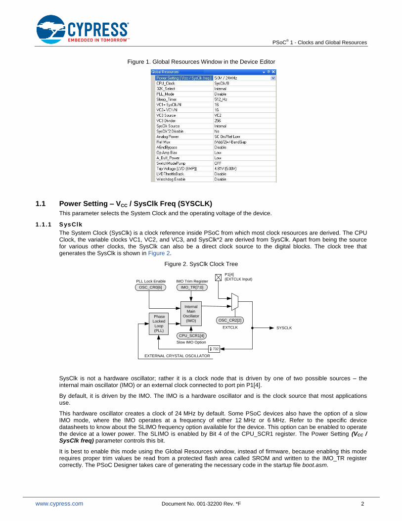
Figure 1. Global Resources Window in the Device Editor
1.1 Power Setting – VCC / SysClk Freq (SYSCLK)
This parameter selects the System Clock and the operating voltage of the device.
1.1.1 SysClk
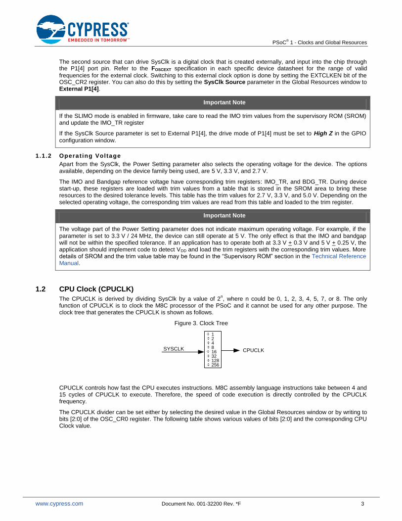
The System Clock (SysClk) is a clock reference inside PSoC from which most clock resources are derived. The CPU Clock, the variable clocks VC1, VC2, and VC3, and SysClk*2 are derived from SysClk. Apart from being the source for various other clocks, the SysClk can also be a direct clock source to the digital blocks. The clock tree that generates the SysClk is shown in Figure 2.
Figure 2. SysClk Clock Tree
SysClk is not a hardware oscillator; rather it is a clock node that is driven by one of two possible sources – the internal main oscillator (IMO) or an external clock connected to port pin P1[4].
By default, it is driven by the IMO. The IMO is a hardware oscillator and is the clock source that most applications use.
This hardware oscillator creates a clock of 24 MHz by default. Some PSoC devices also have the option of a slow IMO mode, where the IMO operates at a frequency of either 12 MHz or 6 MHz. Refer to the specific device datasheets to know about the SLIMO frequency option available for the device. This option can be enabled to operate the device at a lower power. The SLIMO is enabled by Bit 4 of the CPU_SCR1 register. The Power Setting (VCC / SysClk freq) parameter controls this bit.
It is best to enable this mode using the Global Resources window, instead of firmware, because enabling this mode requires proper trim values be read from a protected flash area called SROM and written to the IMO_TR register correctly. The PSoC Designer takes care of generating the necessary code in the startup file boot.asm.
Phase
Locked
Loop
(PLL)
Internal
Main
Oscillator
(IMO)
IMO Trim RegisterPLL Lock Enable
732
EXTCLK
P1[4]
(EXTCLK Input)
IMO_TR[7:0]OSC_CR0[6]
OSC_CR2[2]
Slow IMO Option
CPU_SCR1[4]
EXTERNAL CRYSTAL OSCILLATOR
SYSCLK
PSoC® 1 - Clocks and Global Resources
www.cypress.com Document No. 001-32200 Rev. *F 3
The second source that can drive SysClk is a digital clock that is created externally, and input into the chip through the P1[4] port pin. Refer to the FOSCEXT specification in each specific device datasheet for the range of valid
frequencies for the external clock. Switching to this external clock option is done by setting the EXTCLKEN bit of the OSC_CR2 register. You can also do this by setting the SysClk Source parameter in the Global Resources window to External P1[4].
Important Note
If the SLIMO mode is enabled in firmware, take care to read the IMO trim values from the supervisory ROM (SROM) and update the IMO_TR register
If the SysClk Source parameter is set to External P1[4], the drive mode of P1[4] must be set to High Z in the GPIO
configuration window.
1 .1 .2 Operat ing Voltage
Apart from the SysClk, the Power Setting parameter also selects the operating voltage for the device. The options available, depending on the device family being used, are 5 V, 3.3 V, and 2.7 V.
The IMO and Bandgap reference voltage have corresponding trim registers: IMO_TR, and BDG_TR. During device start-up, these registers are loaded with trim values from a table that is stored in the SROM area to bring these resources to the desired tolerance levels. This table has the trim values for 2.7 V, 3.3 V, and 5.0 V. Depending on the selected operating voltage, the corresponding trim values are read from this table and loaded to the trim register.
Important Note
The voltage part of the Power Setting parameter does not indicate maximum operating voltage. For example, if the parameter is set to 3.3 V / 24 MHz, the device can still operate at 5 V. The only effect is that the IMO and bandgap will not be within the specified tolerance. If an application has to operate both at 3.3 V + 0.3 V and 5 V + 0.25 V, the application should implement code to detect VDD and load the trim registers with the corresponding trim values. More details of SROM and the trim value table may be found in the “Supervisory ROM” section in the Technical Reference Manual.
1.2 CPU Clock (CPUCLK)
The CPUCLK is derived by dividing SysClk by a value of 2n, where n could be 0, 1, 2, 3, 4, 5, 7, or 8. The only
function of CPUCLK is to clock the M8C processor of the PSoC and it cannot be used for any other purpose. The clock tree that generates the CPUCLK is shown as follows.
Figure 3. Clock Tree
CPUCLK controls how fast the CPU executes instructions. M8C assembly language instructions take between 4 and 15 cycles of CPUCLK to execute. Therefore, the speed of code execution is directly controlled by the CPUCLK frequency.
The CPUCLK divider can be set either by selecting the desired value in the Global Resources window or by writing to bits [2:0] of the OSC_CR0 register. The following table shows various values of bits [2:0] and the corresponding CPU Clock value.
CPUCLK
12481632128256
SYSCLK
PSoC® 1 - Clocks and Global Resources
www.cypress.com Document No. 001-32200 Rev. *F 4
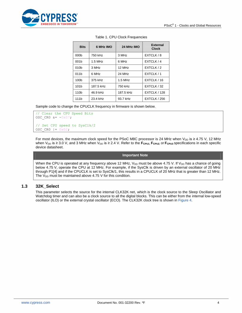
Table 1. CPU Clock Frequencies
Bits 6 MHz IMO 24 MHz IMO External Clock
000b 750 kHz 3 MHz EXTCLK / 8
001b 1.5 MHz 6 MHz EXTCLK / 4
010b 3 MHz 12 MHz EXTCLK / 2
011b 6 MHz 24 MHz EXTCLK / 1
100b 375 kHz 1.5 MHz EXTCLK / 16
101b 187.5 kHz 750 kHz EXTCLK / 32
110b 46.9 kHz 187.5 kHz EXTCLK / 128
111b 23.4 kHz 93.7 kHz EXTCLK / 256
Sample code to change the CPUCLK frequency in firmware is shown below.
// Clear the CPU Speed Bits
OSC_CR0 &= ~0x07;
// Set CPU speed to SysClk/2
OSC_CR0 |= 0x02;
For most devices, the maximum clock speed for the PSoC M8C processor is 24 MHz when VDD is ≥ 4.75 V, 12 MHz when VDD is ≥ 3.0 V, and 3 MHz when VDD is ≥ 2.4 V. Refer to the FCPU1, FCPU2, or FCPU3 specifications in each specific
device datasheet.
Important Note
When the CPU is operated at any frequency above 12 MHz, VDD must be above 4.75 V. If VDD has a chance of going below 4.75 V, operate the CPU at 12 MHz. For example, if the SysClk is driven by an external oscillator of 20 MHz through P1[4] and if the CPUCLK is set to SysClk/1, this results in a CPUCLK of 20 MHz that is greater than 12 MHz. The VDD must be maintained above 4.75 V for this condition.
1.3 32K_Select
This parameter selects the source for the internal CLK32K net, which is the clock source to the Sleep Oscillator and Watchdog timer and can also be a clock source to all the digital blocks. This can be either from the internal low-speed oscillator (ILO) or the external crystal oscillator (ECO). The CLK32K clock tree is shown in Figure 4.
PSoC® 1 - Clocks and Global Resources
www.cypress.com Document No. 001-32200 Rev. *F 5
Figure 4. CLK32K and SLEEP Clocks
The ILO is a circuit on the PSoC device that has a nominal frequency of 32 kHz. However, this clock has a low accuracy of -50% to +100%. Refer to the F32K1 specification in each specific device datasheet. This error has three
sources: a coarse initial trim, a large temperature drift, and a large supply voltage drift. The drifts mentioned are not characterized.
The ILO uses little power and, therefore, is useful for managing CPU sleep and wakeup cycles. When the PSoC is put into sleep mode, the CPU and IMO circuitry are powered down and the ILO is the only oscillator that is left functioning.
CLK32K can be driven by the ILO if its accuracy meets the application’s needs.
To give the CLK32K better accuracy, an external crystal oscillator (ECO) can be added to a design. This is nothing but an external 32.768 kHz crystal and a couple of load capacitors. This allows CLK32K to be very accurate. However, not all PSoC families have the option of adding an ECO. You can consult each specific device datasheet to see if an ECO can be added. For more information on adding an ECO, see application note AN2027 – PSoC
® 1 -
32.768 kHz External Crystal Oscillator.
The ECO must be stable before it can be connected to the CLK32K net. The boot.asm file provides a 1 second delay to allow the ECO to stabilize.
1.4 PLL_Mode
This parameter enables or disables a phase-locked loop (PLL) that can make the IMO very precise when an ECO is used. The PLL multiplies the ECO frequency by 732 to generate an IMO frequency of 23.986 MHz. Refer to the FPLL
specification in each specific device datasheet. Refer to the SysClk tree in Figure 2, which shows the implementation of the PLL.
The PLL can be enabled either in the Global Resources window or by setting Bit 6 of the OSC_CR0 register. Bit 7 of OSC_CR2 controls the PLL lock time and jitter.
Important Notes
The external crystal must be stable before enabling the PLL. A 16 ms delay is necessary for the PLL to lock. The CPU should not be operated above 3 MHz during this lock time. The boot.asm takes care of these delays.
To avoid jitter on the PLL certain PCB layout guidelines must be strictly followed. See AN2027 – PSoC
® 1 - 32.768 kHz External Crystal Oscillator for the PCB guidelines. In addition, refer to Chapter 11
(Phase-Locked Loop) in the Technical Reference Manual.
External
Crystal
Oscillator
(ECO)
32 kHz SelectSLEEP
Internal
Low Speed
Oscillator
(ILO)
P1[1] P1[0]
ILO Trim Register
Vdd
CLK32K
OSC_CR0[7]ILO_TR[7:0]
ECO Trim Register
ECO_TR[7:0]
Vdd
Sleep Clock Divider
OSC_CR0[4:3]
26
29
212
215
PSoC® 1 - Clocks and Global Resources
www.cypress.com Document No. 001-32200 Rev. *F 6
1.5 Sleep_Timer (SLEEP)
The SLEEP clock (also known as the “sleep timer”) is often used to generate infrequent interrupts that wake the CPU from sleep mode. As can be seen in Figure 4, the SLEEP clock is derived from CLK32K with a divider equal to 2
6, 2
9,
212
, or 215
resulting in frequencies of 512 Hz, 64 Hz, 8 Hz, or 1 Hz.
This SLEEP clock frequency can be selected with the Sleep_Timer parameter in the Global Resource window. It can
also be changed by modifying the OSC_CR0 register. As the SLEEP clock is derived from the CLK32K net, the SLEEP clock has the same accuracy of CLK32K. When CLK32K is driven by the ILO, the SLEEP clock is highly inaccurate.
The SLEEP clock can be enabled to generate interrupts with each rising edge of the clock. This interrupt may be used to implement rough timekeeping functions when derived from ILO and highly precise timekeeping functions, such as RTC, while derived from ECO.
To implement the ISR for Sleep interrupt:
1. In the main code, enable the Sleep interrupt by writing to the INT_MSK0 register by using the M8C_EnableIntMask macro.
In assembly:
M8C_EnableIntMask INT_MSK0 INT_MSK0_SLEEP
In C:
M8C_EnableIntMask(INT_MSK0, INT_MSK0_SLEEP);
2. Write the ISR Function:
In assembly:
Sleep_ISR:
push A
push X
; ISR Code
pop X
pop A
reti
In C:
// Declare Sleep_ISR as ISR
#pragma interrupt_handler Sleep_ISR
void Sleep_ISR(void)
{
// ISR code goes here
}
3. Open boot.tpl and modify the Sleep interrupt vector. Replace the `@INTERRUPT_25` string with ljmp to the ISR
function. Save the boot.tpl file and Generate application code. If the ISR is written in C, add an underscore before the ISR name. If written in assembly, the underscore is not required.
For assembly ISR:
org 64h ;Sleep Timer Interrupt Vector
ljmp Sleep_ISR
reti
PSoC® 1 - Clocks and Global Resources
www.cypress.com Document No. 001-32200 Rev. *F 7
For C ISR
org 64h ;Sleep Timer Interrupt Vector
ljmp _Sleep_ISR
reti
Important Note
When changes are made in boot.asm, these changes are overwritten when the application code is generated next time. Boot.tpl is the template file from which PSoC Designer generates boot.asm. If the boot.tpl file is modified, changes made to the boot.tpl will always reflect in the boot.asm file.
There is a user module in PSoC Designer called SleepTimer in the Misc Digital section of user modules. This user
module provides a set of API functions to configure and use the SLEEP clock and its functionality.
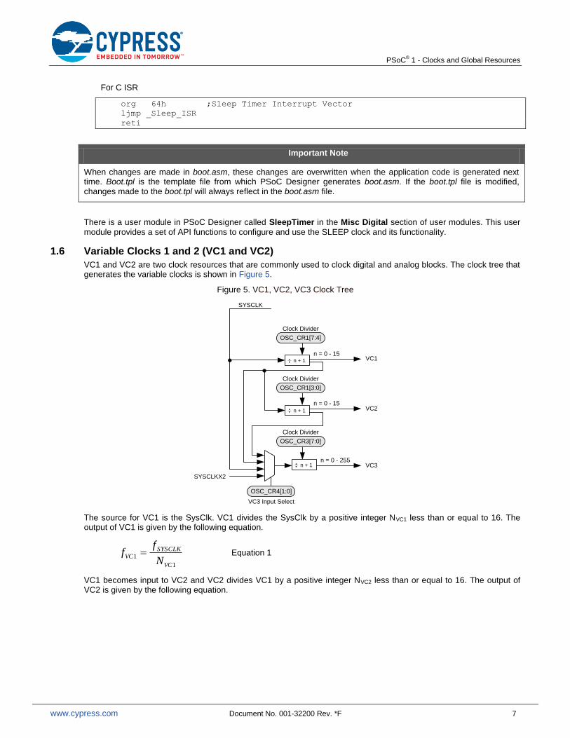
1.6 Variable Clocks 1 and 2 (VC1 and VC2)
VC1 and VC2 are two clock resources that are commonly used to clock digital and analog blocks. The clock tree that generates the variable clocks is shown in Figure 5.
Figure 5. VC1, VC2, VC3 Clock Tree
The source for VC1 is the SysClk. VC1 divides the SysClk by a positive integer NVC1 less than or equal to 16. The output of VC1 is given by the following equation.
1
1
VC
SYSCLKVC
N
ff Equation 1
VC1 becomes input to VC2 and VC2 divides VC1 by a positive integer NVC2 less than or equal to 16. The output of VC2 is given by the following equation.
VC1
VC2
SYSCLK
VC3
SYSCLKX2
VC3 Input Select
Clock Divider
OSC_CR1[7:4]
Clock Divider
OSC_CR1[3:0]
Clock Divider
OSC_CR3[7:0]
n = 0 - 15
n = 0 - 15n + 1
n + 1
n + 1n = 0 - 255
OSC_CR4[1:0]
PSoC® 1 - Clocks and Global Resources
www.cypress.com Document No. 001-32200 Rev. *F 8
2
1
2
VC
VCVC
N
ff Equation 2
The VC1 and VC2 dividers can be set either by using the VC1=SysClk/N and VC2=VC1/N parameters in the Global
Resources window or by writing to the OSC_CR1 register. Bits [7:4] of the register set the VC1 divider by taking the value held in those bits of the register and adding one. Bits [3:0] of the OSC_CR1 register set the VC2 divider by taking the value held in those bits of the register and adding one.
The sample code to change the VC1 and VC2 dividers is shown as follows.
// Change VC1 divider to 10
OSC_CR1 &= ~0xF0;
OSC_CR1 |= 0x90;
// Change VC2 divider to 8
OSC_CR1 &= ~0x0F;
OSC_CR1 |= 0x07;
The VC1 and VC2 frequencies can be modified any time with firmware to change the clock frequencies. During this change, the circuit design guarantees that there are no runt pulses or glitches generated on VC1 or VC2. This is because the new NVC1 or NVC2 does not take effect until the VC1 or VC2 clock period is complete.
1.7 VC3_Source and VC3 Divider
VC3 is another programmable clock, similar to VC1 and VC2, but is more flexible and offers more functionality. As seen in Figure 5, the input to VC3 can be SYSCLK, SYSCLKX2, VC1, or VC2. The divisor, NVC3, can be any positive
integer less than or equal to 256. These features give VC3 a large range of frequencies. The following equation shows how the VC3 clock frequency is derived, where fx is the frequency of the clock from which VC3 is derived
(SYSCLK, SYSCLKX2, VC1, or VC2).
3
3
VC
xVC
N
ff Equation 3
The input to VC3 can be selected either by using the VC3_Source parameter in the Global Resources window or by writing to bits [1:0] in the OSC_CR4 register. The VC3 divider value may be set either by using the VC3_Divider
parameter in the Global Resources window or by writing to the OSC_CR3 register. Sample code to change VC3 clock source and divider is shown as follows.
// Set VC2 as VC3 clock source
OSC_CR4 = 0x02;
// Set VC3 divider to 200
OSC_CR3 = 0xC7;
For more details on OSC_CR3 and OSC_CR4 registers please refer Technical Reference Manual.
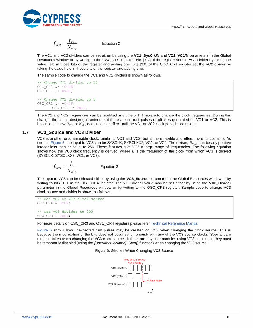
Figure 6 shows how unexpected runt pulses may be created on VC3 when changing the clock source. This is because the modification of the bits does not occur synchronously with any of the VC3 source clocks. Special care must be taken when changing the VC3 clock source. If there are any user modules using VC3 as a clock, they must be temporarily disabled (using the [UserModuleName]_Stop() function) when changing the VC3 source.
Figure 6. Glitches When Changing VC3 Source
Runt Pulse
Time of VC3 Source
Mux Change
Time
VC1 (1.5MHz)
VC2 (500kHz)
VC3 (Divider = 1)
PSoC® 1 - Clocks and Global Resources
www.cypress.com Document No. 001-32200 Rev. *F 9
Changing the VC3 divider does not result in any runt pulses.
Interrupts can be enabled to occur on each rising edge of VC3. These interrupts are enabled by setting bit 7 of the INT_MSK0 register. The boot.tpl file must also be modified to add code to the VC3 vector in the interrupt vector table.
To implement ISR for VC3:
1. In the main code, enable the VC3 interrupt by writing to the INT_MSK0 register by using the M8C_EnableIntMask macro.
In assembly:
M8C_EnableIntMask INT_MSK0 INT_MSK0_VC3
In c:
M8C_EnableIntMask(INT_MSK0, INT_MSK0_VC3);
2. Write the ISR Function:
In assembly:
VC3_ISR:
push A
push X
; ISR Code
pop x
pop A
reti
In C:
// Declare VC3_ISR as ISR
#pragma interrupt_handler VC3_ISR
void VC3_ISR(void)
{
// ISR code goes here
}
3. Open boot.tpl and modify the VC3 interrupt vector. Replace the `@INTERRUPT_6` string with ljmp to the ISR
function. Save the boot.tpl file and Generate application code. If the ISR is written in C, add an underscore before the ISR name. If written in assembly, the underscore is not required.
For assembly ISR:
org 18h ;VC3 Interrupt Vector
ljmp VC3_ISR
reti
For C ISR
org 18h ;VC3 Interrupt Vector
ljmp _VC3_ISR
reti
When not used for any purpose, VC3 must be configured for the lowest possible frequency by setting its divider to 256 and source to VC2. This uses less power in the PSoC. The same principle is also true of VC1 and VC2.
PSoC® 1 - Clocks and Global Resources
www.cypress.com Document No. 001-32200 Rev. *F 10
1.8 SysClk Source
As stated in the earlier section on SysClk, the SYSCLK net can have two sources, the IMO and the External Clock on P1[4]. The source can be selected either by using the SysClk Source parameter in the Global Resources window or
by writing to the EXTCLKEN bit in OSC_CR2 register. The sample code to select the SysClk source is given as follows.
// Select external P1[4] as SysClk source
OSC_CR2 |= OSC_CR2_EXTCLKEN;
When the SysClk Source is set to External P1[4], make sure to set the drive mode of P1[4] to High Z (not “High-Z Analog”) and connect the external clock to P1[4].
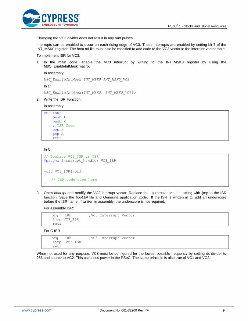
1.9 SysClk*2 Disable
There is a frequency doubler circuit in the PSoC that generates a frequency twice the SYSCLK frequency. As stated in the section on SysClk, the SYSCLK is either generated by the IMO or an external clock. In either case, SYSCLKX2 has the frequency of the SYSCLK frequency multiplied by 2. Since the IMO (24 MHz) is usually used to generate SYSCLK, SYSCLKX2 often has a frequency of 48 MHz. The clock tree that generates SysClk*2 is shown as follows.
Figure 7. Sysclk*2 Clock Tree
To save power, this frequency doubler may be disabled if it is not used, either in the Global Resources Window by selecting Yes to the Disable SysClk*2 parameter or by setting the “SYSCLKX2 DIS” bit in the OSC_CR2 register.
Sample code to disable and enable SysClk*2 in firmware:
// Set the "SYSCLKX2 DIS" BIT to disable SysClk*2
OSC_CR2 |= OSC_CR2_SYSCLKX2DIS;
// Clear the "SYSCLKX2 DIS" BIT to enable SysClk*2
OSC_CR2 &= ~OSC_CR2_SYSCLKX2DIS;
1.10 Watchdog Enable
Watchdog timer (WDT) is used to recover from CPU crashes or from halt state by asserting a reset on the CPU.
The WDT can be enabled either in PSoC Designer using the Watchdog Enable parameter in the Global Resources
window or in application code by executing the following macro.
M8C_EnableWatchDog
The WDT is based on a counter that counts three sleep timer events. The WDT circuit is designed to assert a hardware reset on the device after the three sleep timer interrupts, unless the watchdog is cleared in firmware.
The application code must take care of clearing the WDT at least once within the watchdog overflow interval. For example, if the Sleep Interval is set to 64 Hz, one sleep interval will be equal to 15.625 ms. Considering the +100% tolerance of the ILO, the sleep interval could be as low as 7.8 ms. Watchdog overflow time is 3 * 7.8 ms = 23.4 ms. So, the application code must clear the Watchdog timer at least once in 23.4 ms by calling the below macro.
M8C_ClearWDT
Once the WDT is enabled, it can only be disabled by an external reset (XRES) or a power-on reset (POR). A WDT reset leaves the WDT enabled. Therefore, if the WDT is used in an application, all code (including initialization code) must be written as though the WDT is enabled.
Note: Changing the sleep timer interval also affects the WDT interval. For more information on WDT, refer to Chapter 12 in the Technical Reference Manual, “Sleep and WDT.”
SYSCLKX2Clock
Doubler
SYSCLKX2 Disable
OSC_CR2[0]
SYSCLK
PSoC® 1 - Clocks and Global Resources
www.cypress.com Document No. 001-32200 Rev. *F 11
2 Other Global Parameters
In the previous sections, we described various global resources related to clocks in the PSoC. Now, let us look at the analog and other global resources.
2.1 Analog Power
An analog reference generator inside PSoC generates AGND, REFHI, and REFLO voltages for the Continuous Time (CT) blocks and Switched Capacitor (SC) Blocks to operate. The block diagram of this generator is shown in Figure 8.
Figure 8. Analog Reference Generator
The Analog Power parameter sets the power at which this Analog Reference operates and also if the CT blocks and SC blocks are turned ON or OFF. The following table shows the various options available under this parameter.
Table 2. Analog Power Setting
Value Description
All Off Reference generator, CT Blocks and SC Blocks are off
SC Off / Ref Lo SC Blocks off, CT Blocks on, Reference Generator at low power
SC Off / Ref Med SC Blocks off, CT Blocks on, Reference Generator at Medium power
SC Off / Ref High SC Blocks off, CT Blocks on, Reference Generator at high power
SC On / Ref Lo SC Blocks on, CT Blocks on, Reference Generator at low power
SC On / Ref Med SC Blocks on, CT Blocks on, Reference Generator at Medium power
SC On / Ref High SC Blocks on, CT Blocks on, Reference Generator at high power
The reference power setting should be greater than or equal to the highest power setting of the analog resources in the design. Operating a continuous time block or switched capacitor block, at high power results in the best performance, but also the highest power consumption. Similarly operating at low power results in least power consumption, but less performance.
For example, when a PGA is operated at high power, the slew rate is 9.5 V/µs and the power consumption of the PGA is 2.083 mA. When the PGA is operated at low power, the power consumption comes down to 142 µA, but the slew rate also reduces to 0.6 V/µs. See the specific analog user module datasheets for Power setting versus Performance.
A good rule of thumb is to start designing with the analog reference power set to high and later reduce the power based on power versus performance requirements.
Vbandgap
Vdd/2
P2[6]
Vdd
Vss
RefHi to
Analog
Blocks
RefLo to
Analog
Blocks
AGND
P2[4] (External Cap)
Vbandgap
P2[4]
x1
x1
x1.6
x2
4 and 2 Analog Columns
8.1K8.1K
PSoC® 1 - Clocks and Global Resources
www.cypress.com Document No. 001-32200 Rev. *F 12
For detailed information about the Analog Power, see the application note AN2219 – PSoC® 1 Selecting Analog
Ground and Reference and Chapter 21 of the Technical Reference Manual, “Analog Reference.”
Important Notes
If the design uses any analog resource that is placed in a switched capacitor block, the Analog power must be set to SC On / Ref_x. Setting the power to SC Off / Ref x will disable the switched capacitor blocks.
The reference power should be set to the same level as the highest power analog resource in the design. For example, if a design has a PGA operating at Medium power and an ADC operating at High power, the Analog power must be set to SC On / Reference High.
2.2 Ref Mux
This parameter enables the user to select the analog ground and the input range of the analog blocks. See Figure 8.
The Reference Generator generates three voltages, AGND, which is the analog ground for all the analog blocks, RefHi and RefLo, which sets the range of the analog resources.
These voltages are derived from VDD, a 1.3-V bandgap reference generator, or external voltages connected to P2[4] and P2[6].
For example, if VDD = 5.0 V and RefMux is set to VDD/2 ± Bandgap, this sets AGND to 2.5 V, RefHi to 3.8 V, and RefLo to 1.2 V. This means that the allowed input range for the analog resources is from 1.2 V to 3.8 V.
Setting RefMux to VDD/2 ± VDD/2 enables ratiometric operation but the accuracy of the PSoC depends on the noise level on the supply lines.
For detailed information about ReMux setting, see application note AN2219 – PSoC® 1 Selecting Analog Ground and
Reference and Chapter 21 in the Technical Reference Manual, “Analog Reference.”
2.3 AGndBypass
When AGND Bypass is set to Enabled, pin P2[4] is tristated. An external capacitor connected between P2[4] and VSS reduces the noise at the AGND input by approximately 18 dB.
Typical values for the bypass capacitor are 0.01 µF and should not exceed 0.1 µF.
For detailed information about noise levels and noise reduction, see the application note AN2224 – PSoC
® 1 - Lower Noise Continuous Time Signal Processing. For more information on analog references,
see Chapter 21 in the Technical Reference Manual, “Analog References.”
2.4 Opamp Bias
This parameter changes the opamp bias level and is controlled by Bit 6 of the ARF_CR register. Table 3 describes the properties of opamp bias level options.
Table 3. Opamp Bias Levels
Bias Level Properties
Low Bias Less power consumption and high voltage swing.
High Bias High frequency operation and faster slew rate. Lower output impedance. Typically used for filters where the center frequency or corner frequency is greater than 50 kHz
As a rule of thumb, set the opamp bias to low when starting a design. If high-frequency operation and high slew rate are desired, set this parameter to High.
For more information on Analog References, see Chapter 21 in the Technical Reference Manual, “Analog References.”
2.5 A_Buff_Power
This setting determines the power level of the analog output buffers. Setting the buffer power to “low” reduces power consumption but also reduces the drive capability of the buffers. Setting the buffer to power “high” increases power consumption and improves drive capacity.
PSoC® 1 - Clocks and Global Resources
www.cypress.com Document No. 001-32200 Rev. *F 13
2.6 Switch Mode Pump (SMP)
This parameter turns ON and OFF the internal boost converter used to generate supply voltage from a low voltage battery with a few external components.
For more information on the PSoC Switch Mode Pump, see Chapter 31 in the Technical Reference Manual, “Switch Mode Pump (SMP).”
2.7 Trip Voltage[LVD(SMP)]
This parameter sets the trip voltage for low-voltage detect (LVD) and operating voltage for the SMP, respectively.
LVD interrupt is triggered when VDD falls below the value selected for this parameter.
For example, if the LVD value is selected as 4.64 V, the LVD interrupt is triggered when VDD falls below 4.64 V. If LVD interrupt is enabled in the INT_MSK0 register, the CPU branches to the LVD interrupt vector in boot.asm and executes the LVD ISR code. By default, a “halt” instruction is placed in the LVD interrupt vector. So, if the LVD interrupt is enabled and if this interrupt is triggered, the CPU halts and the only way to come out of ‘halt’ is to reset the PSoC.
The user can edit the interrupt vector and put in custom code to execute when an LVD interrupt occurs. For example, the ISR can detect power fail and write critical information to an EEPROM.
To write an ISR for LVD -
1. In main code, enable the LVD interrupt by writing to the INT_MSK0 register by using the M8C_EnableIntMask macro.
In assembly:
M8C_EnableIntMask INT_MSK0 INT_MSK0_VOLTAGE_MONITOR
In c:
M8C_EnableIntMask(INT_MSK0,INT_MSK0_VOLTAGE_MONITOR);
2. Write the ISR Function:
In assembly:
LVD_ISR:
push A
push X
; ISR Code
pop x
pop A
reti
In C:
// Declare LVD_ISR as ISR
#pragma interrupt_handler LVD_ISR
void LVD_ISR(void)
{
// ISR code goes here
}
3. Open boot.tpl and modify the LVD interrupt vector. Replace the `halt` string with ljmp to the ISR function.
Save the boot.tpl file and Generate application code. If the ISR is written in C, add an underscore before the ISR
name. If written in assembly, the underscore is not required.
PSoC® 1 - Clocks and Global Resources
www.cypress.com Document No. 001-32200 Rev. *F 14
For assembly ISR:
org 04h ;LVD Interrupt Vector
ljmp LVD_ISR
reti
For C ISR
org 04h ;LVD Interrupt Vector
ljmp _LVD_ISR
reti
The SMP level denotes the target VDD voltage for the SMP system. If the VDD level is below this value, the SMP begins operation.
2.8 LVD Throttleback
When enabled, this parameter automatically resets the CPU speed to SysClk/8. This parameter can be particularly useful when the CPU is operated at 24 MHz.
As discussed in the earlier section on CPU clock, when CPU operates at 24 MHz, VDD has to be above 4.75 V. If the LVD threshold is set to 4.81 V and LVD Throttleback is enabled, when VDD goes below 4.81 V, the CPU speed will automatically be reduced to 3 MHz, preventing the CPU from operating outside the rated specification. An ISR maybe written for the LVD to wait for the VDD to go above 4.81 V before setting the CPU speed back to 24 MHz.
For more information on the PSoC Low Voltage Detect, see Chapter 32 in the Technical Reference Manual, “POR and LVD.”
3 Global Resources Specific to CY8C20xx7 and CY8C20xx6 Devices
The CY8C20xx7 and CY8C20xx6 devices have the following additional parameters in the Global Resources window.
For details about CY8C20xx7 registers refer CY8C20xx7 Technical Reference Manual.
For details about CY8C20xx6 registers refer CY8C20xx6A Technical Reference Manual.
3.1 Interrupt mode
Selects the GPIO interrupt mode for all pins to be enabled either on “Low” or when the output is changed from previous read status. This parameter modifies the I/O_CFG register.
3.2 P1[0] Data Output
This parameter selects the source that drives the signal on P1[0]. Sleep interrupt signal or Comparator 0 output can be routed to P1[0]. This parameter modifies the OUT_P1 register.
3.3 P1[2] Data Output
This parameter selects the source that drives the signal on P1[2]. The Main System Clock (SYSCLK) or either CapSense Output signal (CS_OUT is selected by CS_OUT[1:0] bits in CS_CR0 register) or CapSense clock depending upon bit 7 in the PRS_CR register. This parameter modifies the OUT_P1 register.
3.4 P1[4] Data Output
This parameter selects the source that drives the signal on P1[4]. The Comparator 1 output or Relaxation oscillator output can be routed to P1[4]. This parameter modifies OUT_P1 register.
3.5 P1[6] Data Output
This parameter selects the source that drives the signal on P1[6]. The Timer output or CLK32 can be routed to P1[6]. This parameter modifies the OUT_P1 register.
3.6 POR Voltage
This parameter selects the voltage below which the chip remains in the reset state. This parameter modifies the VLT_CR register.
PSoC® 1 - Clocks and Global Resources
www.cypress.com Document No. 001-32200 Rev. *F 15
4 Related Documents
More information about the various Global Resources may be found in the following references:
1. The PSoC Technical Reference Manual contains a large body of reference material related to PSoC microcontrollers.
2. Each specific PSoC device datasheet lists specifications related to different parameters explained in the Application note
3. AN2027 – PSoC® 1 - 32.768 kHz External Crystal Oscillator is an application note describing the best practices
for adding an external crystal to a PSoC design.
4. AN2219 – PSoC® 1 Selecting Analog Ground and Reference outlines the applicability of each reference setting
to typical system designs.
5. AN2224 – PSoC® 1 - Lower Noise Continuous Time Signal Processing is an application note that provides an
introduction to microcontroller noise phenomena, specifics on PSoC noise parameters and ways to optimize system design to minimize effects of on-chip noise
About the Author Name: M. Ganesh Raja
Title: Applications Engineer Senior Principal
Background: Ganesh did his Diploma in Electronics and Communications Engineering from Motilal Nehru Govt. Polytechnic in Pondicherry India. He has about 20 years of experience in
Analog circuit design and
Microcontrollers. He also writes a blog “PSoC Hacker” in cypress website.
PSoC® 1 - Clocks and Global Resources
www.cypress.com Document No. 001-32200 Rev. *F 16
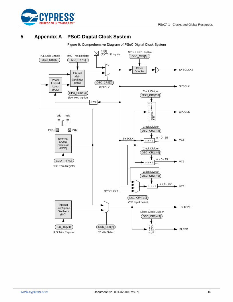
5 Appendix A – PSoC Digital Clock System
Figure 9. Comprehensive Diagram of PSoC Digital Clock System
External
Crystal
Oscillator
(ECO)
Phase
Locked
Loop
(PLL)
SYSCLK
SYSCLKX2
32 kHz Select
CPUCLK
VC1
VC2
SLEEP
Internal
Main
Oscillator
(IMO)
Internal
Low Speed
Oscillator
(ILO)
IMO Trim RegisterPLL Lock Enable
P1[1] P1[0]
ILO Trim Register
Vdd
CLK32K
SYSCLK
VC3
SYSCLKX2
VC3 Input Select
Clock
Doubler
732
EXTCLK
P1[4]
(EXTCLK Input)
OSC_CR0[7]ILO_TR[7:0]
ECO Trim Register
ECO_TR[7:0]
IMO_TR[7:0]OSC_CR0[6]
Vdd
OSC_CR2[2]
Clock Divider
OSC_CR0[2:0]
Clock Divider
OSC_CR1[7:4]
Clock Divider
OSC_CR1[3:0]
Clock Divider
OSC_CR3[7:0]
Sleep Clock Divider
OSC_CR0[4:3]
26
29
212
215
SYSCLKX2 Disable
OSC_CR2[0]
Slow IMO Option
CPU_SCR1[4]
n = 0 - 15
n = 0 - 15n + 1
n + 1
12481632128256
n + 1n = 0 - 255
OSC_CR4[1:0]
PSoC® 1 - Clocks and Global Resources
www.cypress.com Document No. 001-32200 Rev. *F 17
Document History
Document Title: AN32200 – PSoC® 1 - Clocks and Global Resources
Document Number: 001-32200
Revision ECN Orig. of Change
Submission Date
Description of Change
** 1504463 BTK 09/23/2007 New Spec.
*A 3176744 BTK 02/15/2011 The contents of AN2221 (001-33759) has been merged into this AN.
*B 3603870 GRAA 04/30/2012 Arranged the sections to match with the order of parameters as found in the Global Resources window in PSD.
Added sample code snippet at various sections to show how the parameters may be changed in firmware.
Added step by step instructions to implement ISRs for SLEEP, VC3 and LVD interrupts.
Added relevant clock tree sections under various clock sections.
Added block diagram of the reference generator in the Analog Power section.
Updated template.
*C 4492948 DIMA 09/04/2014 Added support for CY8C20xx7 and CY8C20xx6 devices. Removed reference to AN2354.
*D 4621922 ARVI 01/13/2015 Corrected the figure reference in the Ref Mux section.
Updated to new template.
*E 4769023 GRAA 05/27/2015 Updated Document Title to read as “AN32200 – PSoC® 1 - Clocks and Global
Resources”.
Updated reference application note titles.
Updated Abstract.
Updated CPU Clock (CPUCLK) (Updated description).
Updated VC3_Source and VC3 Divider (Updated description).
Updated SysClk Source (Updated description).
Updated Analog Power (Updated description and Table 2).
Updated Trip Voltage[LVD(SMP)] (Updated description).
Updated Global Resources Specific to CY8C20xx7 and CY8C20xx6 Devices (Renamed “Global Resources” as “Global Resources Specific to CY8C20xx7 and CY8C20xx6 Devices” and updated the same section).
Updated to new template.
Completing Sunset Review.
*F 5713671 AESATMP9 04/26/2017 Updated logo and copyright.
PSoC® 1 - Clocks and Global Resources
www.cypress.com Document No. 001-32200 Rev. *F 18
Worldwide Sales and Design Support
Cypress maintains a worldwide network of offices, solution centers, manufacturer’s representatives, and distributors. To find the office closest to you, visit us at Cypress Locations.
Products
ARM® Cortex
® Microcontrollers cypress.com/arm
Automotive cypress.com/automotive
Clocks & Buffers cypress.com/clocks
Interface cypress.com/interface
Internet of Things cypress.com/iot
Memory cypress.com/memory
Microcontrollers cypress.com/mcu
PSoC cypress.com/psoc
Power Management ICs cypress.com/pmic
Touch Sensing cypress.com/touch
USB Controllers cypress.com/usb
Wireless Connectivity cypress.com/wireless
PSoC® Solutions
PSoC 1 | PSoC 3 | PSoC 4 | PSoC 5LP | PSoC 6
Cypress Developer Community
Forums | WICED IOT Forums | Projects | Videos | Blogs | Training | Components
Technical Support
cypress.com/support
All other trademarks or registered trademarks referenced herein are the property of their respective owners.
Cypress Semiconductor 198 Champion Court San Jose, CA 95134-1709
©Cypress Semiconductor Corporation, 2007-2017. This document is the property of Cypress Semiconductor Corporation and its subsidiaries, including Spansion LLC (“Cypress”). This document, including any software or firmware included or referenced in this document (“Software”), is owned by Cypress under the intellectual property laws and treaties of the United States and other countries worldwide. Cypress reserves all rights under such laws and treaties and does not, except as specifically stated in this paragraph, grant any license under its patents, copyrights, trademarks, or other intellectual property rights. If the Software is not accompanied by a license agreement and you do not otherwise have a written agreement with Cypress governing the use of the Software, then Cypress hereby grants you a personal, non-exclusive, nontransferable license (without the right to sublicense) (1) under its copyright rights in the Software (a) for Software provided in source code form, to modify and reproduce the Software solely for use with Cypress hardware products, only internally within your organization, and (b) to distribute the Software in binary code form externally to end users (either directly or indirectly through resellers and distributors), solely for use on Cypress hardware product units, and (2) under those claims of Cypress’s patents that are infringed by the Software (as provided by Cypress, unmodified) to make, use, distribute, and import the Software solely for use with Cypress hardware products. Any other use, reproduction, modification, translation, or compilation of the Software is prohibited.
TO THE EXTENT PERMITTED BY APPLICABLE LAW, CYPRESS MAKES NO WARRANTY OF ANY KIND, EXPRESS OR IMPLIED, WITH REGARD TO THIS DOCUMENT OR ANY SOFTWARE OR ACCOMPANYING HARDWARE, INCLUDING, BUT NOT LIMITED TO, THE IMPLIED WARRANTIES OF MERCHANTABILITY AND FITNESS FOR A PARTICULAR PURPOSE. To the extent permitted by applicable law, Cypress reserves the right to make changes to this document without further notice. Cypress does not assume any liability arising out of the application or use of any product or circuit described in this document. Any information provided in this document, including any sample design information or programming code, is provided only for reference purposes. It is the responsibility of the user of this document to properly design, program, and test the functionality and safety of any application made of this information and any resulting product. Cypress products are not designed, intended, or authorized for use as critical components in systems designed or intended for the operation of weapons, weapons systems, nuclear installations, life-support devices or systems, other medical devices or systems (including resuscitation equipment and surgical implants), pollution control or hazardous substances management, or other uses where the failure of the device or system could cause personal injury, death, or property damage (“Unintended Uses”). A critical component is any component of a device or system whose failure to perform can be reasonably expected to cause the failure of the device or system, or to affect its safety or effectiveness. Cypress is not liable, in whole or in part, and you shall and hereby do release Cypress from any claim, damage, or other liability arising from or related to all Unintended Uses of Cypress products. You shall indemnify and hold Cypress harmless from and against all claims, costs, damages, and other liabilities, including claims for personal injury or death, arising from or related to any Unintended Uses of Cypress products.
Cypress, the Cypress logo, Spansion, the Spansion logo, and combinations thereof, WICED, PSoC, CapSense, EZ-USB, F-RAM, and Traveo are trademarks or registered trademarks of Cypress in the United States and other countries. For a more complete list of Cypress trademarks, visit cypress.com. Other names and brands may be claimed as property of their respective owners.
Related Documents