Clock Distribution Scheme using Coplanar Transmission Lines Victor Cordero Sunil P Khatri Department of ECE Texas A&M University [email protected] [email protected]

Clock Distribution Scheme using Coplanar Transmission Lines Victor Cordero Sunil P Khatri Department of ECE Texas A&M University [email protected].
Dec 20, 2015
Welcome message from author
This document is posted to help you gain knowledge. Please leave a comment to let me know what you think about it! Share it to your friends and learn new things together.
Transcript

Clock Distribution Scheme using Coplanar Transmission Lines
Victor CorderoSunil P Khatri
Department of ECETexas A&M University
[email protected]@tamu.edu
Introduction
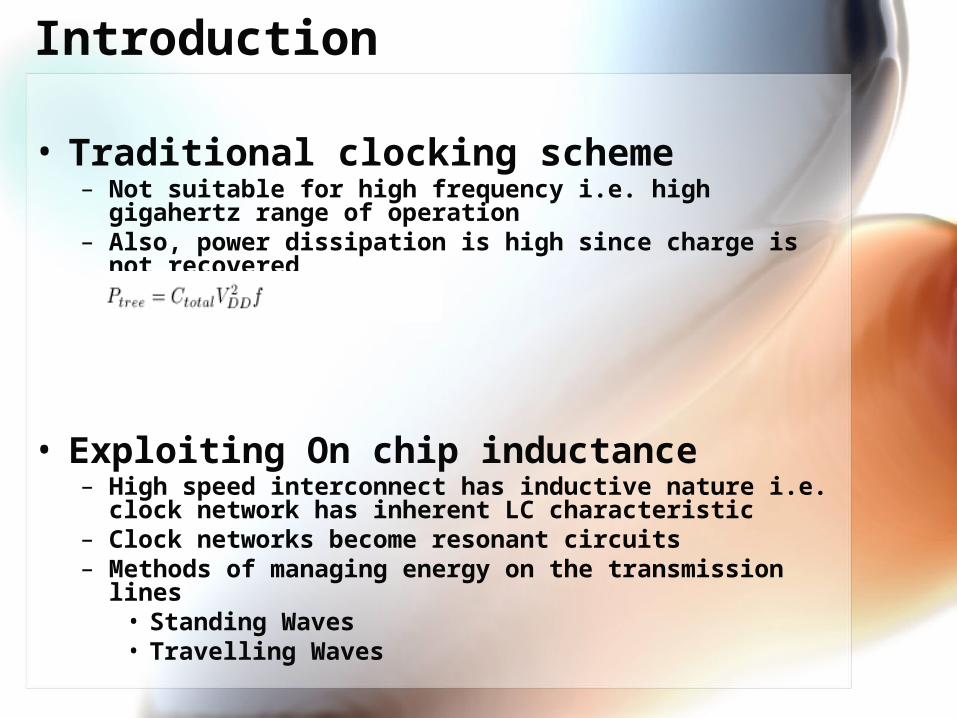
• Traditional clocking scheme– Not suitable for high frequency i.e. high gigahertz range of
operation– Also, power dissipation is high since charge is not
recovered
• Exploiting On chip inductance– High speed interconnect has inductive nature i.e. clock
network has inherent LC characteristic– Clock networks become resonant circuits– Methods of managing energy on the transmission lines
• Standing Waves• Travelling Waves
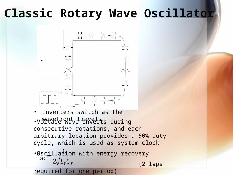
Classic Rotary Wave Oscillator
• Inverters switch as the wavefront travels
•Voltage wave inverts during consecutive rotations, and each arbitrary location provides a 50% duty cycle, which is used as system clock.
•Oscillation with energy recovery
(2 laps required for one period)TT
oscCL
F2
1

The Phase Shift Problem
SingleInverter pair
Mobiuscrossing
Full amplitude
clock
0°
Full amplitude
clock
45°
90°
135°
180°
225°
270°
315°
Questions to Classic Rotary Clock
1) Why do we need to propagate a square wave?
Can we “encode” a clock in a differential pair more efficiently?
2) Can we get phase = 0 at all points along the ring regardless of distance?
3) How to tap into (“decode”) the clock signal from the transmission line ring?

Standing Wave Oscillators
λ/4 standing wave oscillation
Forward waves (from inverter) travels along the transmission line, hits the short and gets a reverse wave back
Forward and reverse superpose and we obtain a standing wave along Z direction
Sinusoid wave propagation
Length (l)
Vol
tage
0
VAC
Forward wave
Standing wave (across wire length)
Reflected wave
Residual traveling wave
Z
Z

Short Terminated Ring
Clock recoverer
ckt
SingleInverter pair
Differential transmissionLine segment
Short termination
1 2 3
24
4 5
Full amplitude clock
391.9um side
65.33um
391.9um side
•Differential Line Total Linear Length = 1567.2 um
•Each segment 65.3um long
•25 probe locations, each with full differential amplifier and load cap (5 not used)
•Used a 90 nm technology (BSIM3) (1V)
•Simulated in HSPICE
•Corner effect assumed negligible
•Single sided voltage polarity per half cycle across ring
Short – Termination Results
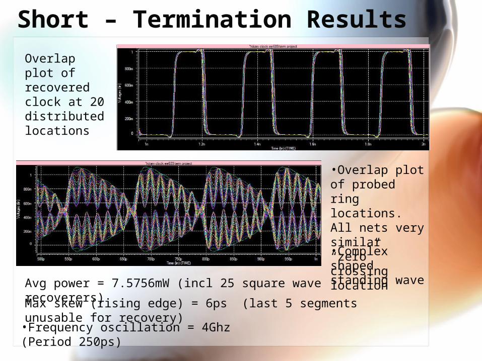
Avg power = 7.5756mW (incl 25 square wave recoverers)
Overlap plot of recovered clock at 20 distributed locations
Max skew (rising edge) = 6ps (last 5 segments unusable for recovery)
•Frequency oscillation = 4Ghz (Period 250ps)
•Overlap plot of probed ring locations. All nets very similar “zero” crossing location
•Complex shaped standing wave

Our Contribution : Differential Mobius T-line
•Replace short connect to a mobius interconect at the end of TL
Can we go faster for the same total length?
•We create a “virtual” short at the halfpoint from the source
•We create a two phase system. Flip differential amplifier connections on the left side to get same phase for recovered clock
Clockrecoverer
ckt
SingleInverter pair
Differential transmissionLine segment
Mobiuscrossing
1 2
3
24
4
5
Full amplitude
clock
391.9um side
65.33um
391.9um side
Virtual “zero” crossing (phase change
+-
Clockrecoverer
ckt
Full amplitude
clock
+-

Our Differential Mobius DesignAvg power = 8.201mW (including 25 square wave recoverers)
Max skew (rising edge) = 3.1ps (middle 4 segments unusable for recovery)
•Frequency oscillation = 9.8Ghz (Period 101.9ps). Duty cycle <50%

Mobius Versus Short-Termination
• Mobius termination works at 9GHz, while Short-circuit termination works at 4GHz. Why?– Short termination has a significant impedance mismatch
• Hence a spurious traveling wave results.– Mobius termination has a lower impedance mismatch at the end-
point. • This mismatch is due to the presence of the cross-coupled inverter
pair, but not due to short circuit termination. • The spurious traveling wave has lower amplitude than in the short-
circuit termination case
Short Termination
Mobius Termination

Our Clock Recovery Circuit
Differential input 2 VDC ~=0.5v VAC~0.6v to 40mV (very wide range able)
Differential input 1
Current mirror
Bias generator
Sharp edge generators and buffer
1V
1V
Min size to loading in gates.and to cascaded inverters
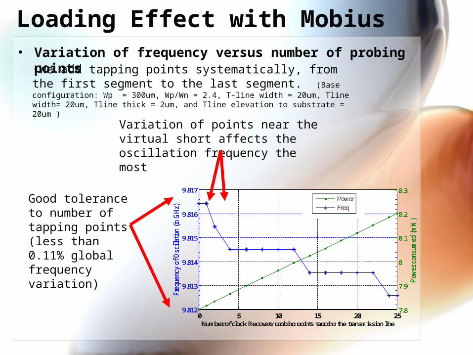
Loading Effect with Mobius• Variation of frequency versus number of probing points
Variation of points near the virtual short affects the oscillation frequency the most
•We add tapping points systematically, from the first segment to the last segment. (Base configuration: Wp = 300um, Wp/Wn = 2.4, T-line width = 20um, Tline width= 20um, Tline thick = 2um, and Tline elevation to substrate = 20um )
Good tolerance to number of tapping points (less than 0.11% global frequency variation)
0 5 10 15 20 259.812
9.813
9.814
9.815
9.816
9.817
Number of clock Recovery probing points tapping the transmission line
Fre
quen
cy o
f O
scill
atio
n (in
GH
z)
0 5 10 15 20 257.8
7.9
8
8.1
8.2
8.3
Pow
er c
onsu
med
(m
W)
Power
Freq
0 5 10 15 20 259.812
9.813
9.814
9.815
9.816
9.817
Number of clock Recovery probing points tapping the transmission line
Fre
quen
cy o
f O
scill
atio
n (in
GH
z)
0 5 10 15 20 257.8
7.9
8
8.1
8.2
8.3
Pow
er c
onsu
med
(m
W)
Power
Freq

Long ring configurations
Total ring length(um)
T-line width(um)
Wp(um)
Beta(wp/wn)
Freq(GHz)
Global Skewmax(ps)
Power (mW)
Non recoverable nodes
4927.2 40 120 2.4 9.090 0.986 3.640 3
5407.2 40 100 2.0 9.022 2.870 3.400 3
5407.2 40 100 2.1 9.075 2.99 3.300 3
5407.2 40 100 2.4 9.266 3.31 3.120 3
Our Standing wave Clock configurations
Standard Rotary Clock configurations
Total ring length(um)
T-line width(um)
Wp(um)
Beta(wp/wn)
Freq(GHz)
Global Skewmax(ps)
Power(mW)
Non recoverable nodes
4927.2 40 120 2.4 3.68 25 3.54 3
5407.2 40 100 2.0 3.80 8.1 3.28 2
5407.2 40 100 2.1 3.89 7.86 3.09 2
5407.2 40 100 2.4 4.07 11.3 2.91 1
Total ring length(um)
T-line width(um)
Wp(um)
Beta(wp/wn)
Freq(GHz)
Power con sumed(mW)
4927.2 20 10 1.22 7.97 2.49
5407.2 30 10 1.02 7.75 2.57
5407.2 20 10 1.22 7.51 2.46
5407.2 25 10 0.9 7.34 2.81
Shorted wave Clock configurations
•For rotary wave a sweep was performed in order to track the maximum achievable frequency for the studied length (at 25 repeater pairs)

Design Cookbook
• We performed extensive experiments with varying – Conductor widths– Ring length– Inverter size– PMOS to NMOS size ratio
• Details are in the paper

Summary• We have developed an improved resonant clock
architecture by eliminating the phase shift complexity (of the Rotary Clock) across the ring
• Our ring structure maintains a single standing wave with a virtual short. – Doubles operating frequency compared to a standing
wave oscillator with a short circuit termination
• We developed custom high speed differential to square wave amplifiers for the wide range of tapping point types along the ring. The clock recovery adds almost no loading effect on the differential transmission line
• Studied the performance of our architecture as a function of various circuit parameters.

Thank you!

Considerations at 9GHZ
•We could double the total loop length (when using mobius) and keep the same frequency as the shorted loop (for bigger chips)
•Output of the clock not fully square wave due to our CMOS inverter performance in high frequency. Variable falling edge due to decreased swing at differential stage for “weak” probe points
•The cascaded output inverter stage (of the clock recovery circuit) has a hard time creating sharp square edges at 9Ghz.

Ring Length Effects in Mobius
•If length is too long, the standing wave won’t form.
•If high frequencies required we can link multiple standing wave rings
•The architecture allows us to have scalable frequencies by simply adjusting the total ring length within a range
1500 2000 2500 3000 3500 4000 4500 50004
5
6
7
8
9
1010
Total transmission line ring loop lenght (in um)
Osc
illat
ion
freq
uenc
y (in
GH
z)
1500 2000 2500 3000 3500 4000 4500 50007.6
7.7
7.8
7.9
8
8.1
8.2
8.3
8.48.4
Pow
er c
onsu
med
(in
mW
)
powerWith 25 recovery circuits
1500 2000 2500 3000 3500 4000 4500 50004
5
6
7
8
9
1010
Total transmition-line ring loop lenght (in um)
Osc
illat
ion
Fre
quen
cy (in
GH
z)
1500 2000 2500 3000 3500 4000 4500 50007
7.25
7.5
7.75
8
Pow
er c
onsu
mpt
ion
(in m
W)
powerWithout recovery circuits
1500 2000 2500 3000 3500 4000 4500 50001
2
3
4
5
6
7
Total transmission line lenght (in um)
Max
imum
ske
w m
easu
red
(in u
m)
With 25 recovery circuits

Ring Width Effects in Mobius•If we increase wire resistance, more energy needed to keep oscillation going.
2 4 6 8 10 12 14 16 18 206
6.5
7
7.5
8
8.5
9
9.5
1010
Fre
quen
cy o
f O
scill
atio
n (in
GH
z)
2 4 6 8 10 12 14 16 18 208
9
10
11
12
Transmission line width (in um)
Pow
er c
onsu
med
(in
mW
)
power
W<= 20um
•Power consumption monotonically decreases until to W=24um
20 22 24 26 28 30 32 34 36 38 409.5
10
10.5
11
11.5
12
Transmission Line width (in um)
Fre
quen
cy o
f os
cilla
tion
(in G
Hx)
20 22 24 26 28 30 32 34 36 38 407.8
7.9
8
8.1
8.2
8.3
Pow
er c
onsu
med
(in
mW
)
power
W>= 20um
•Ring configuration stays the same as before. Fully tapped ring used.
20 22.5 25 27.5 30 32.5 35 37.5 40402
2.5
3
3.5
4
4.5
Transmission line width (in um)
Ave
rage
max
imum
ske
w (i
n ps
) W>= 20um

PMOS/NMOS width effects
200 250 300 350 400 4506
7
8
9
10
11
1212
PMOS device width in um (with Wp/Wn=2.4 constant)
Osc
illat
ion
Fre
quen
cy (in
GH
z)
200 250 300 350 400 4506
7
8
9
10
11
1212
Pow
er c
onsu
med
(in
mW
)
power
200 250 300 350 400 4501.5
1.75
2
2.25
2.5
2.75
3
3.25
PMOS device width (in um) with Wp/Wn =2.4
Max
imum
Ske
w m
easu
red
(in p
s)
•Power consumpion grows close to linear when PMOS width grows.
•Bigger drivers increase our total ring capacitance, making the oscillation frequency drop
Max skew gets reduced by stronger drivers.
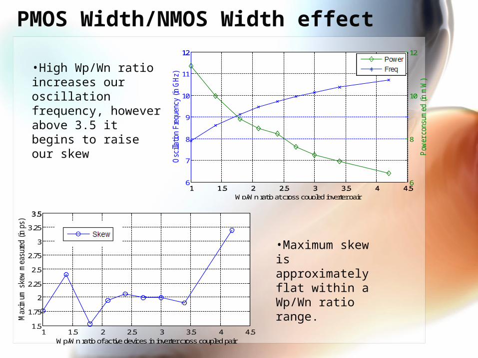
PMOS Width/NMOS Width effect
1 1.5 2 2.5 3 3.5 4 4.56
7
8
9
10
11
1212
Wp/Wn ratio at cross coupled inverter pair
Osc
illat
ion
Fre
quen
cy (in
GH
z)
1 1.5 2 2.5 3 3.5 4 4.56
8
10
12
Pow
er c
onsu
med
(in
mW
)
power
1 1.5 2 2.5 3 3.5 4 4.51.5
1.75
2
2.25
2.5
2.75
3
3.25
3.53.5
Wp/Wn ratio of active devices in inverter cross coupled pair
Max
imum
ske
w m
easu
red
(in p
s)
•High Wp/Wn ratio increases our oscillation frequency, however above 3.5 it begins to raise our skew
•Maximum skew is approximately flat within a Wp/Wn ratio range.
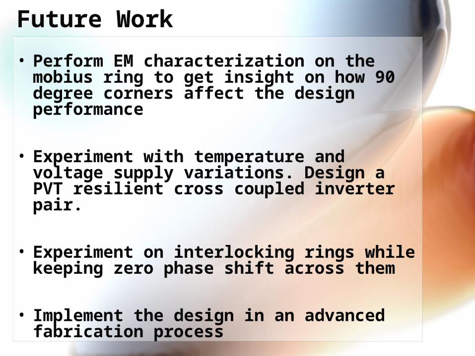
Future Work
• Perform EM characterization on the mobius ring to get insight on how 90 degree corners affect the design performance
• Experiment with temperature and voltage supply variations. Design a PVT resilient cross coupled inverter pair.
• Experiment on interlocking rings while keeping zero phase shift across them
• Implement the design in an advanced fabrication process

Current on-going work•Frequency stepping.
Direct tuning of the frecuency through modification of the ring capacitance. This provides wide range of frequency stepping
Clockrecoverer
ckt
1 2
3
24
4
5
Full amplitude
clock
+-
Clockrecoverer
ckt
Full amplitude
clock
+-
Variable CapFrequencyMatcher
ReferenceExt. clock
0 2 4 6 8 101
2
3
4
5
6
7
8
9
Capacitance Value (pF)
Osc
illat
ion
Fre
quen
cy (
GH
z)
Frequency Tunning through direct Capacitance tuning for standing wave
Ring Frequency
Related Documents