This work is licensed under a Creative Commons Attribution 3.0 License. For more information, see http://creativecommons.org/licenses/by/3.0/. This article has been accepted for publication in a future issue of this journal, but has not been fully edited. Content may change prior to final publication. Citation information: DOI 10.1109/TPEL.2016.2641260, IEEE Transactions on Power Electronics 1 Class-E Half-Wave Zero dv/dt Rectifiers for Inductive Power Transfer George Kkelis, Student Member, IEEE, David C. Yates, Member, IEEE, and Paul D. Mitcheson, Senior Member, IEEE. Abstract—This paper analyses and compares candidate zero dv/dt half-wave Class-E rectifier topologies for integration into multi-MHz inductive power transfer (IPT) systems. Further- more, a hybrid Class-E topology comprising advantageous prop- erties from all existing Class-E half-wave zero dv/dt rectifiers is analysed for the first time. From the analysis, it is shown that the hybrid Class-E rectifier provides an extra degree of design freedom which enables optimal IPT operation over a wider range of operating conditions. Furthermore, it is shown that by designing both the hybrid and the current driven rectifiers to operate below resonance provides a low deviation input reactance and inherent output voltage regulation with duty cycle allowing efficient IPT operation over wider dc load range than would otherwise be achieved. A set of case studies demonstrated the following performances: 1) For a constant dc load resistance, a receiving end efficiency of 95 % was achieved when utilising the hybrid rectifier, with a tolerance in required input resistance of 2.4% over the tested output power range (50 to 200 W). 2) For a variable dc load in the range of 100 % to 10 %, the hybrid and current driven rectifiers presented an input reactance deviation less than 2% of the impedance of the magnetising inductance of the inductive link respectively and receiving end efficiencies greater than 90 %. 3) For a constant current in the receiving coil, both the hybrid and the current driven rectifier achieve inherent output voltage regulation in the order of 3% and 8% of the nominal value respectively, for a variable dc load range from 100 % to 10 %. I. I NTRODUCTION W EAKLY coupled inductive links, Fig. 1, tend to operate in the low MHz region in order to increase their link efficiency (η link ), [1]–[3]. The optimal link efficiency (η link,opt ) of a particular inductive link geometry occurs when the receiving coil (L rx ) is tuned at the frequency of the generated magnetic field and the ratio of the ac load resistance (R ac ) to the reactance of the tuning capacitor (C rx ) satisfies a specific value (α opt ) [1]. The α opt value depends upon the coupling factor (k) between the transmitting coil (L tx ) and L rx , the unloaded quality factors of the two coils and the tuning method of L rx , parallel (Fig. 1a) or series (Fig. 1b) [1]. When a rectifier is added to an inductive link, its input resistance will be the ac load and must therefore be evaluated according to maximum link efficiency requirements. Furthermore, the rectifier topology should be efficient at the frequency of operation, be compatible with the output type of the tuned receiving coil, voltage output for parallel tuned George Kkelis, David C. Yates and Paul D. Mitcheson are with the Control and Power Research Group, Electrical and Electronic Engineering Department, Imperial College London, http://www.imperial.ac.uk/wireless- power. Email: {g.kkelis13}{david.yates}{paul.mitcheson}@imperial.ac.uk. i ac L tx L rx C rx R ac,par k (a) Parallel tuned receiving coil - compatible with voltage driven rectifiers. i ac L tx L rx C rx R ac,ser k (b) Series tuned receiving coil - compatible with current driven rectifiers. Fig. 1: Inductive link circuit configurations. receiving coil (Fig. 1a) or current output for series tuned coil (Fig. 1b), and its input reactance should be absorbed by C rx such that the tuning of L rx will be unaffected. Class-E rectifiers, [4], [5], are very popular in multi-MHz resonant converters [6]–[13] due to their efficient soft switch- ing capability and low electromagnetic footprint. Due to their success in resonant converters, the utilisation of Class-E recti- fiers is gaining popularity in weakly coupled multi-MHz IPT systems [14]–[16]. This section provides a general description of the operation of Class-E rectifiers. It then examines and presents the various developments of the topologies presented in literature. Fig. 2 summarises the circuit configurations of the reviewed Class-E rectifiers. Fig. 3 classifies the reported Class-E designs according to their operating frequency and maximum output power and Table I provides further details about the operation, performance and targeted application of the topologies of Fig. 3. Class-E zero dv/dt rectifiers use a capacitor (C), or a capacitive network of total capacitance C in the case of the hybrid topology (Fig. 2a), to achieve zero rate of change of the voltage across the diode when it is reverse biased. An inductor (L) is used for the circulation of the dc load current when the diode is forward biased. A filter capacitor (C f ) is used to stabilise the output voltage. The operation of Class-E zero dv/dt rectifiers can be classified in three modes based on a variable A r , defined as the ratio of the resonance frequency of the LC network (ω r ) to the operating frequency (ω). The first mode is at the point where ω r equals to ω, A r is equal to unity, and the rectifier is therefore operating at

Welcome message from author
This document is posted to help you gain knowledge. Please leave a comment to let me know what you think about it! Share it to your friends and learn new things together.
Transcript

This work is licensed under a Creative Commons Attribution 3.0 License. For more information, see http://creativecommons.org/licenses/by/3.0/.
This article has been accepted for publication in a future issue of this journal, but has not been fully edited. Content may change prior to final publication. Citation information: DOI 10.1109/TPEL.2016.2641260, IEEETransactions on Power Electronics
1
Class-E Half-Wave Zero dv/dt Rectifiers forInductive Power Transfer
George Kkelis, Student Member, IEEE, David C. Yates, Member, IEEE,and Paul D. Mitcheson, Senior Member, IEEE.
Abstract—This paper analyses and compares candidate zerodv/dt half-wave Class-E rectifier topologies for integration intomulti-MHz inductive power transfer (IPT) systems. Further-more, a hybrid Class-E topology comprising advantageous prop-erties from all existing Class-E half-wave zero dv/dt rectifiersis analysed for the first time. From the analysis, it is shownthat the hybrid Class-E rectifier provides an extra degree ofdesign freedom which enables optimal IPT operation over a widerrange of operating conditions. Furthermore, it is shown that bydesigning both the hybrid and the current driven rectifiers tooperate below resonance provides a low deviation input reactanceand inherent output voltage regulation with duty cycle allowingefficient IPT operation over wider dc load range than wouldotherwise be achieved. A set of case studies demonstrated thefollowing performances: 1) For a constant dc load resistance, areceiving end efficiency of 95% was achieved when utilising thehybrid rectifier, with a tolerance in required input resistance of2.4% over the tested output power range (50 to 200W). 2) Fora variable dc load in the range of 100% to 10%, the hybrid andcurrent driven rectifiers presented an input reactance deviationless than 2% of the impedance of the magnetising inductanceof the inductive link respectively and receiving end efficienciesgreater than 90%. 3) For a constant current in the receiving coil,both the hybrid and the current driven rectifier achieve inherentoutput voltage regulation in the order of 3% and 8% of thenominal value respectively, for a variable dc load range from100% to 10%.
I. INTRODUCTION
WEAKLY coupled inductive links, Fig. 1, tend to operatein the low MHz region in order to increase their
link efficiency (ηlink), [1]–[3]. The optimal link efficiency(ηlink,opt) of a particular inductive link geometry occurswhen the receiving coil (Lrx) is tuned at the frequency ofthe generated magnetic field and the ratio of the ac loadresistance (Rac) to the reactance of the tuning capacitor (Crx)satisfies a specific value (αopt) [1]. The αopt value dependsupon the coupling factor (k) between the transmitting coil(Ltx) and Lrx, the unloaded quality factors of the two coilsand the tuning method of Lrx, parallel (Fig. 1a) or series(Fig. 1b) [1]. When a rectifier is added to an inductive link,its input resistance will be the ac load and must therefore beevaluated according to maximum link efficiency requirements.Furthermore, the rectifier topology should be efficient at thefrequency of operation, be compatible with the output typeof the tuned receiving coil, voltage output for parallel tuned
George Kkelis, David C. Yates and Paul D. Mitcheson are with theControl and Power Research Group, Electrical and Electronic EngineeringDepartment, Imperial College London, http://www.imperial.ac.uk/wireless-power. Email: [email protected].
iac Ltx Lrx Crx Rac,park
(a) Parallel tuned receiving coil - compatible with voltage drivenrectifiers.
iac Ltx LrxCrx
Rac,serk
(b) Series tuned receiving coil - compatible with current drivenrectifiers.
Fig. 1: Inductive link circuit configurations.
receiving coil (Fig. 1a) or current output for series tuned coil(Fig. 1b), and its input reactance should be absorbed by Crxsuch that the tuning of Lrx will be unaffected.
Class-E rectifiers, [4], [5], are very popular in multi-MHzresonant converters [6]–[13] due to their efficient soft switch-ing capability and low electromagnetic footprint. Due to theirsuccess in resonant converters, the utilisation of Class-E recti-fiers is gaining popularity in weakly coupled multi-MHz IPTsystems [14]–[16]. This section provides a general descriptionof the operation of Class-E rectifiers. It then examines andpresents the various developments of the topologies presentedin literature. Fig. 2 summarises the circuit configurations ofthe reviewed Class-E rectifiers. Fig. 3 classifies the reportedClass-E designs according to their operating frequency andmaximum output power and Table I provides further detailsabout the operation, performance and targeted application ofthe topologies of Fig. 3.
Class-E zero dv/dt rectifiers use a capacitor (C), or acapacitive network of total capacitance C in the case of thehybrid topology (Fig. 2a), to achieve zero rate of changeof the voltage across the diode when it is reverse biased.An inductor (L) is used for the circulation of the dc loadcurrent when the diode is forward biased. A filter capacitor(Cf ) is used to stabilise the output voltage. The operation ofClass-E zero dv/dt rectifiers can be classified in three modesbased on a variable Ar, defined as the ratio of the resonancefrequency of the LC network (ωr) to the operating frequency(ω). The first mode is at the point where ωr equals to ω, Aris equal to unity, and the rectifier is therefore operating at

This work is licensed under a Creative Commons Attribution 3.0 License. For more information, see http://creativecommons.org/licenses/by/3.0/.
This article has been accepted for publication in a future issue of this journal, but has not been fully edited. Content may change prior to final publication. Citation information: DOI 10.1109/TPEL.2016.2641260, IEEETransactions on Power Electronics
2
vin
CsiCs
Cp
iCp
LiL
D
+
−vD
iD
Cf
iCf
Rdc
−
+
Vdc
Idc
(a) Hybrid rectifier (HVDR).
iin C
iC
LiL
D
+
−vD
iD
Cf
iCf
Rdc
−
+
Vdc
Idc
(b) Current driven rectifier (CDR).
vin
CiC
LiL
D
+
−vD
iD
Cf
iCf
Rdc
−
+
Vdc
Idc
(c) Voltage driven rectifier with series capacitor(series-C VDR).
vin
L
iLD
iD
C
+ −vD
iC
Cf
iCf
Rdc
−
+
Vdc
Idc
(d) Voltage driven rectifier with series inductor(series-L VDR).
Fig. 2: Hybrid and Conventional Class-E half-wave zero dv/dt rectifiers.
10−1 100 101 102
10−1
100
101
102
103
[this work]
[12][13]
[17]
[8][9], [18]
[11][10]
[19]
[20]
[21]
[22]
[23]
[24]
[6][15], [25]
[26], [27]
[16]
[7][28]
[29]
Frequency [MHz]
Pow
er[W
]
Hybrid topology - Fig. 2a; Current driven - Fig. 2b; Voltage driven series capacitor - Fig. 2c; Voltage driven series inductor - Fig. 2d
Fig. 3: Power vs frequency map for reported half-wave Class-E rectifiers.
TABLE I: Further characteristics of reported Class-E rectifiers in literature.
Rectifier Ref. Full Load Diode Technology Application η [%] Comments on Developed Rectifiers
Fig. 2a [this work] 77 V; 2.6 A SiC Schottky IPT1 95∗∗ Most efficient design from the case studies. Rectifier developed to provide optimal loading to the IPT of [2].
Fig. 2a [12] 28 V; 0.89 A Schottky RPC2 82.5∗ Rectifier developed in a SEPIC converter as the dual circuit of Fig. 2d.
Fig. 2b [8] 12 V; 0.83 A Si Schottky RPC 75∗ Designed to present a resistive input impedance by using a finite impedance inductor.
Fig. 2b [9] 12 V; 2 A Si Schottky RPC 75∗ Two circuits with resistive input impedances, as in [8], added in a resistance compression configuration.
Fig. 2b [11] 65 V; 7.69 A SiC Schottky RPC 81.6∗ Resistive input impedance design in a push-pull configuration.
Fig. 2b [10] 33 V; 6 A SiC Schottky RPC 82.5∗ Same design as in [8] but L was replaced with an auto-transformer.
Fig. 2b [13] 5 V; 2 A Silicon Schottky RPC N/A Analysis assuming a finite impedance inductor (L) and development to present a resistive input impedance.
Fig. 2b [17] 5 V; 0.2 A; Si Schottky RPC N/A Analysis of the topology at any duty cycle assuming an infinite impedance inductor (L).
Fig. 2b [19] 28 V; 13.57 A; SiC Schottky RPC 74∗ Same concept as in [10] with increased output power capability.
Fig. 2b [20] 12 V; 1.5 A Si Schottky RPC N/A Topology developed to present low deviation in input phase as the dc load varies between 100 % to 10 %.
Fig. 2b [21] 100 V; 1 A Ultrafast Recovery IPT 90∗ Topology developed for a contactless IPT system based on numerical analysis.
Fig. 2b [22] 24.5 V; 0.82 A Silicon Schottky IPT 84∗ Analysis based on [17] but including component losses. Case study based on a short-range IPT system.
Fig. 2b [25] 60 V; 2.5 A SiC Schottky IPT 90∗∗ Design of the topology with an infinite impedance inductor (L), for presenting optimal loading to the IPT of [2].
Fig. 2c [27] 5 V; 0.1 A Si Schottky RPC 91∗∗ Analysis at any duty cycle of operation with the LC network resonating at the frequency of operation.
Fig. 2c [23] 2.6 V; 0.05 A N/A RPC N/A First implementation of the circuit with an infinite impedance inductor (L).
Fig. 2c [24] 5 V; 0.2 A Fast Recovery RPC N/A Analysis at any duty cycle of operation with an infinite impedance inductor (L).
Fig. 2d [6] 5 V; 10 A N/A RPC 87∗ First developed zero dv/dt Class-E rectifier. Developed from an isolated voltage driven Class-D rectifier.
Fig. 2d [7] 24 V; 2.08 A Si Schottky RPC 81.6∗ Integration of the topology in an isolated converter.
Fig. 2d [15] 140 V; 0.85 A SiC Schottky IPT 90∗∗ Design for operation below resonance to minimise the inductor size required by optimal IPT efficiency.
Fig. 2d [16] 27 V; 0.36 A Si Schottky IPT 94∗∗ State space analysis of the topology and integration in a short-range IPT system.
Fig. 2d [26] 5 V; 0.1 A Si Schottky RPC 88.67∗∗ Topology was analysed at any duty cycle for operation at the resonant frequency of the LC network.
Fig. 2d [18] 33 V; 0.7 A Si Schottky RPC 87∗∗ Topology developed for a VHF boost converter. Maximum reported frequency of operation.
Fig. 2d [28] 11.57 V; 1.16 A MOSFET IRF540 IPT 80∗ Synchronous rectification. Absorption of L in the receiving coil of a short range IPT system.
Fig. 2d [29] 18 V; 0.56 A Si Schottky IPT 92∗∗ Absorption of L in the receiving coil of a contactless IPT system.
1Inductive Power Transfer, 2Resonant Power Converters; ∗System Efficiency, ∗∗Rectifier Efficiency
This work is licensed under a Creative Commons Attribution 3.0 License. For more information, see http://creativecommons.org/licenses/by/3.0/.
This article has been accepted for publication in a future issue of this journal, but has not been fully edited. Content may change prior to final publication. Citation information: DOI 10.1109/TPEL.2016.2641260, IEEETransactions on Power Electronics
3
resonance. In the other two modes the rectifier is operatingaway from resonance and Ar is either smaller than unity, foroperation above resonance, or greater than unity, for operationbelow resonance. The functionality of L varies between thedifferent Class-E topologies. In the hybrid topology of Fig. 2a(HVDR), the current driven topology of Fig. 2b (CDR) andthe voltage driven topology with series capacitor of Fig. 2c(series-C VDR), L functions as a filter inductor and hasa large harmonic distortion in the current through it (iL).When the diode is forward biased, one end of the inductoris clamped to ground causing a constant rate of discharge ofCf through L. When the diode is reverse biased, iL has asinusoidal component superimposed to the output dc current.The magnitude of the ac component of iL increases with Ar.When Ar approaches zero in operation above resonance, thecurrent through L can be assumed to be dc. In the voltagedriven rectifier with a series inductor of Fig. 2d (series-L VDR), the presence of L decreases the harmonic content ofthe current drawn from the voltage source and hence the accomponent of the current through L can be assumed sinusoidalin all operating modes. The sinusoidal current component issuperimposed to the output dc current.
The HVDR (Fig. 2a) was introduced in the case study of[23] where it was compared with the series-C VDR (Fig. 2c).Furthermore, the HVDR was empirically designed for opera-tion at resonance and implemented in a SEPIC converter in[12]. Although not discussed in the aforementioned references,the HVDR is an improved design of the series-C VDR. Unlikethe other rectifier topologies, the series-C VDR does notabsorb the pn junction capacitance of the diode (Cpn) in itsLC network. The non-constant behavior of Cpn with voltagemakes the operation of the series-C VDR non-robust when Cis in the same order of magnitude as Cpn. In the HVDR, Cis split into Cs and Cp. Since an external capacitor is nowput across the diode, Cpn can be physically absorbed by Cp.In this work, the HVDR is analysed for the first time in allClass-E rectifier operating modes, at all duty cycles, for anyratio of Cp to Cs.
In resonant power converter applications, the most widelyused Class-E rectifier is the CDR (Fig. 2b). The topology wasintroduced in [17], where it was analysed at all duty cycleswith an inductor (L) assumed to be of infinite impedance (Aris zero). In [8]–[11], [13] and [20] more properties of thetopology were exploited by utilising an inductor (L) of finiteimpedance. For a specific duty cycle and Ar, the topology canexhibit a resistive input impedance at the frequency operation,[8]–[11] and [13], as otherwise appears resistive and eithercapacitive [17] or inductive [20]. Over a dc load range between100 % to 10 %, and hence a varying duty cycle, the CDR canhave a low input phase deviation by selecting the appropriateAr, [20]. The series-L VDR (Fig. 2d) was introduced in [6],where it was developed from an isolated voltage driven Class-D half-wave rectifier. The analysis of this topology at all dutycycles was reported in [26] for operation at resonance andin [30] for an ω varying around resonance. In [23] the firstimplementation of the series-C VDR (Fig. 2c) is reported. Itsanalysis at all duty cycles is reported in [24] with an L ofinfinite impedance and in [27] for operation at resonance.
Both the CDR (Fig. 2b) and the series-L VDR (Fig. 2d)were developed for IPT applications [15], [16], [21], [22],[25], [28] and [29]. Our work in [15] reports the first Class-Erectifier integrated in a mid-range multi-MHz IPT system. Thecircuit used was the series-L VDR. In [15] the implementationchallenges of L, due to the large required inductance value athigh frequency, were highlighted when the circuit is designedto emulate optimal link efficiency conditions for the inductivelink in [2]. L is easier to fabricate when designing the topologyat an Ar smaller than unity since, the required inductancedecreases. Another improvement was introduced in the shortrange IPT system of [28] for sub-MHz operation, and in thecontactless IPT of [29] for multi-MHz operation, by includingL in the tuned receiving coil. While this method solves theimplementation problem, the receiving coil is never exactlyat resonance. Therefore, the link efficiency drops significantlywhen the coils operate at mid-range distances due to increasedlosses in the transmitting coil caused by the reduced reflectedresistance as a result of the uncompensated reactance of thereceiving coil.
The implementation of L in the other rectifiers of Fig. 2does not impose such a great challenge as in the series-LVDR (Fig. 2d). Our work in [25] presented the design andimplementation of the CDR (Fig. 2b) for the inductive link in[2] as an improvement on [15]. However, since the CDR is acurrent driven topology it will experience higher conductionlosses than the voltage driven rectifiers when designed topresent optimal loading for the same set of coils [1]. The CDRachieved the same efficiency as the series-L VDR but is morerobust to the diode parasitic capacitance [15], [25]. Our studyin [31] showed potential for improvement in the performanceof the receiving end when the HVDR (Fig. 2a) is utilisedinstead of the conventional Class-E rectifiers of Fig. 2.
As can be seen, much work has been reported in the Class-Erectifiers in a range of applications which has highlighted someadvantages, and disadvantages, of the topologies. However,there exists no formal analysis for structured comparison ofthese topologies over a range of operating scenarios. Thispaper provides a design framework for Class-E half-wave zerodv/dt rectifier topologies which allows the designer to selectthe optimal topology based on power levels, frequency ofoperation and inductive link properties. It will also be shownthat rectifiers can be designed to present a low input reactancedeviation and inherent output voltage regulation over a rangeof output load values. While the discussions focus on IPTapplications, the rectifier analysis results are applicable forother applications. Section II, discusses the design of Class-Erectifiers that provides optimal link efficiency conditions andSection III, presents the behavior of rectifier design variablesunder several operating conditions. Section IV then discussesthe case studies that took place after the analysis results ofSection III and finally, Section V presents the conclusions.
II. DESIGN FOR INTEGRATION IN IPT SYSTEMS
For a successful Class-E rectifier integration in an IPTsystem, the input resistance of the topology must be set toan optimal value based on the configuration of the inductive

This work is licensed under a Creative Commons Attribution 3.0 License. For more information, see http://creativecommons.org/licenses/by/3.0/.
This article has been accepted for publication in a future issue of this journal, but has not been fully edited. Content may change prior to final publication. Citation information: DOI 10.1109/TPEL.2016.2641260, IEEETransactions on Power Electronics
4
link. It is mathematically convenient to represent the inputimpedance of the voltage driven Class-E rectifiers as theparallel connection of a reactive component, Xin,p, and theinput resistance, Rin,p. On the other hand, in the current driventopology it is more convenient to present the input impedanceby a series combination between Xin,s and Rin,s [32].
When Class-E rectifiers are designed to provide optimal linkefficiency conditions, designers can select the duty cycle, dr,at full load and variable Ar:
Ar =ωrω. (1)
In the case of the HVDR (Fig. 2a) another degree of freedomis introduced in the selection of variable B defined as:
B =CpCs, (2)
where the sum of the two capacitances is:
C = Cs + Cp. (3)
The passive components in the circuit are then evaluated suchthat the specified conditions are met. The duty cycle dependson the loaded quality factor (Qr) of the rectifier, defined as:
Qr =RdcX
, (4)
where Rdc is the rectifier’s dc load and X is the reactance ofthe series component in the voltage driven topologies (L orC) or in the current driven topology, X is the reactance ofcapacitor C. The relationship between the dc resistance withthe input resistance in the voltage driven rectifiers (assuming100 % efficiency) is given by:
Rdc = 2MV2Rin,p = 2MV
2Rac,par, (5)
where MV is the ratio of output voltage to the peak of theac input voltage (ac to dc voltage gain). In the current driventopology Rdc is given by:
Rdc =Rin,s
2MI2 =
Rac,ser
2MI2 , (6)
where MI is the ratio of output current to the peak of the acinput current (ac to dc current gain). In order to directly relatethe input ac resistance to the required X value, (5) and (6) aresubstituted into (4) and the variables are rearranged such thatan expression is formed relating the ratio of the ac resistanceto the required X value. This ratio will be called input loadedquality factor, Qin, and is given by the following expressions:
Qin =Qr
2MV2 =
Rin,pX
, (7)
for the voltage driven topologies and
Qin = 2MI2Qr =
Rin,sX
, (8)
for the current driven topology. Using the definition of variableAr, the relationship between the reactances forming the LCnetwork is given by:
Ar2 =
XC
XL. (9)
In the case of the HVDR, Cs and Cp are evaluated from (2),(3) and (9). Finally, the ratio of input reactance to X is givenby:
Nin =Xin
X. (10)
The Class-E topologies of Fig. 2, were analysed for op-eration at any duty cycle, dr, and an Ar range between0 to 2, while the analysis of the hybrid Class-E rectifier,Fig. 2a, was also performed as a function of variable B. In themathematical analysis of each rectifier, the diode and passivecomponents were assumed ideal and lossless. The derivationof the design variables follows the same method as presentedin [24], [32]–[34] which is summarised in Appendix A alongwith the equations of the design variables of the rectifiers ofFig. 2.
The choice of 50 % duty cycle at full load is consideredto be optimum by the authors because it provides maximumpower output capability (cPdc
) in Class-E rectifiers and hencefully utilises the device [32]. From this starting point (100 %dc load), the duty cycle can only decrease as Rdc increases.Hence the analysis of this paper has not been applied to dutycycles greater than 50 %.
III. DISCUSSION OF RECTIFIER FEATURES
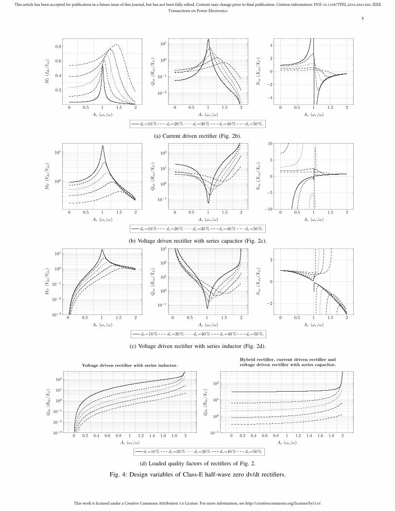
The design variables in (4) - (8) and (10), for the conven-tional Class-E topologies are presented in Fig. 4 as functions ofAr for duty cycle values from 50 % to 10 %, in steps of 10 %.In Fig. 5 the design variables are illustrated as functions ofAr for several values of B at 50 % duty cycle for the HVDR.The loaded quality factor (Qr) is independent of variable Band is therefore the same for the HVDR (Fig. 2a) and theseries-C VDR (Fig. 2c). Also, Qr in the CDR (Fig. 2b) is thesame as in HVDR and the series-C VDR since CDR forms theNorton equivalent circuit of the series-C VDR. Fig. 6 presentsthe diode stresses in half-wave Class-E rectifiers, and so alongwith Figs. 4 & 5, maps out the entire state space of rectifierdesigns and can be utilised to discuss in detail the performanceand trade-offs of different rectifier designs operating across arange of conditions.
Positive and negative features of the candidate rectifiertopologies when operating at duty cycles from 50 % and belowwill now be discussed using Figs. 4, 5 & 6. These discussionsare based on the configuration of the inductive link of [2], theparameters of which are summarised in Table II (the optimalcondition parameters were calculated using [1]).
A. Current Driven Class-E Rectifier (CDR)
As shown in Table I, the CDR (Fig. 2b) is the mostcommonly implemented topology of the conventional half-wave Class-E rectifiers presented in the literature. It haspreviously been designed for values of Ar in the range of 0 to1.42, [8]–[11], [13], [17]. However, a crucial property of thetopology has been missed because as can be seen for Nin inFig. 4a, an Ar between 1.75 to 2 has the additional advantageof compressing the input reactance of the topology, Xin,s, asthe duty cycle decreases below 50 % (as a result of increasingRdc). The maximum deviation in Xin,s is 13 % from its initial
This work is licensed under a Creative Commons Attribution 3.0 License. For more information, see http://creativecommons.org/licenses/by/3.0/.
This article has been accepted for publication in a future issue of this journal, but has not been fully edited. Content may change prior to final publication. Citation information: DOI 10.1109/TPEL.2016.2641260, IEEETransactions on Power Electronics
5
0 0.5 1 1.5 2
0.2
0.4
0.6
0.8
Ar (ωr/ω)
MI(Idc/Iin)
0 0.5 1 1.5 2
10−2
10−1
100
101
Ar (ωr/ω)
Qin
(Rin/X
C)
0 0.5 1 1.5 2
−4
−2
0
2
4
Ar (ωr/ω)
Nin
(Xin/XC)
dr=10% dr=20% dr=30% dr=40% dr=50%.
(a) Current driven rectifier (Fig. 2b).
0 0.5 1 1.5 2
100
101
Ar (ωr/ω)
MV
(Vdc/V
in)
0 0.5 1 1.5 2
10−1
100
101
102
Ar (ωr/ω)
Qin
(Rin/X
C)
0 0.5 1 1.5 2−10
−5
0
5
10
Ar (ωr/ω)
Nin
(Xin/X
C)
dr=10% dr=20% dr=30% dr=40% dr=50%.
(b) Voltage driven rectifier with series capacitor (Fig. 2c).
0 0.5 1 1.5 210−3
10−2
10−1
100
101
Ar (ωr/ω)
MV
(Vdc/V
in)
0 0.5 1 1.5 2
10−1
100
101
102
103
Ar (ωr/ω)
Qin
(Rin/X
L)
0 0.5 1 1.5 2
−2
0
2
Ar (ωr/ω)
Nin
(Xin/X
L)
dr=10% dr=20% dr=30% dr=40% dr=50%.
(c) Voltage driven rectifier with series inductor (Fig. 2d).
0 0.2 0.4 0.6 0.8 1 1.2 1.4 1.6 1.8 210−3
10−2
10−1
100
101
102
Ar (ωr/ω)
Qdc(R
dc/X
L)
Voltage driven rectifier with series inductor.
0 0.2 0.4 0.6 0.8 1 1.2 1.4 1.6 1.8 210−1
100
101
102
Ar (ωr/ω)
Qdc(R
dc/X
C)
Hybrid rectifier, current driven rectifier andvoltage driven rectifier with series capacitor.
dr=10% dr=20% dr=30% dr=40% dr=50%.
(d) Loaded quality factors of rectifiers of Fig. 2.
Fig. 4: Design variables of Class-E half-wave zero dv/dt rectifiers.

This work is licensed under a Creative Commons Attribution 3.0 License. For more information, see http://creativecommons.org/licenses/by/3.0/.
This article has been accepted for publication in a future issue of this journal, but has not been fully edited. Content may change prior to final publication. Citation information: DOI 10.1109/TPEL.2016.2641260, IEEETransactions on Power Electronics
6
0 0.5 1 1.5 2
0.02
0.04
0.06
0.08
0.1
0.12
0.14
Ar (ωr/ω)
MV
(Vdc/Vin)
0 0.5 1 1.5 2101
102
103
Ar (ωr/ω)
Qin
(Rin/X
C)
0 0.5 1 1.5 22
3
4
5
6
7
8
9
10
Ar (ωr/ω)
Nin
(XC
in/XC)
B=2; B=3; B=4; B=5; B=6; B=7.
Fig. 5: Design variables of hybrid Class-E rectifier (Fig. 2a) for 50 % duty cycle.
0 0.5 1 1.5 2
2
2.5
3
3.5
Ar (ωr/ω)
VD,M
/Vdc
0 0.5 1 1.5 20
10
20
30
Ar (ωr/ω)
I D,M
/Idc
0 0.5 1 1.5 2
10−2
10−1
Ar (ωr/ω)
CP
dc(Pdc/V
D,M
/ID,M
)
dr=10% dr=20% dr=30% dr=40% dr=50%.
Fig. 6: Diode stresses for all examined Class-E half-wave topologies.
TABLE II: Characteristics of the inductive link in [2].
Parameter Value
f [MHz] 6.78
k∗ [%] 3.5
Ltx [µH] 4
Lrx [µH] 5.67
Xtx [jΩ] 170.4
Xrx [jΩ] 241.54
Qtx 1300
Qrx 1000
Optimal conditions Value
αopt,ser
(Rac,ser
Xrx
)0.044
αopt,par
(Rac,par
Xrx
)22.77
ηlink,opt [%] 95
Rac,ser [Ω] 10.6
Rac,par [Ω] 5500
Rref [Ω] 6
∗At a center to center coil separation equal to one diameter of the transmitting coil.
value at an Ar equal to 1.75 when the duty cycle changes from50 % to 43 %. When the duty cycle decreases below 43 % thedeviation of input reactance reduces and approaches the inputreactance value for 50 % duty cycle. As Ar increases above1.75 the maximum deviation in Xin,s decreases. The effectof the Xin,s deviation on the receiving resonant tank dependson the absolute value of the input reactance, which dependson XC and thus from (8), on Qin and the required emulatedinput resistance (Rac,ser for the CDR). By evaluating Xin,s
using αopt,ser from Table II and Qin and Nin from Fig. 4a, itcan be seen that a deviation in Xin,s by 13 % will result in aresidual reactance at the receiving end smaller than 1 % of thereactance of Lrx. Therefore, when the CDR is designed for
values of Ar in the range of 1.75 to 2, its effect on the tuningof the receiving coil will be negligible when Rdc increases.
In the same Ar range (1.75 to 2) unlike Xin,s the inputresistance (Rin,s) of the topology will change significantlywith duty cycle. From the definition of Qin and by consideringthe behavior of duty cycle with Rdc, the input resistanceof the topology decreases as Rdc increases. In fact in theaforementioned Ar range, the input resistance of the circuitwill be halved when Rdc is doubled. This behavior of Rin,sprovides an inherent output voltage regulation assuming aconstant input current. The inherent output voltage regula-tion can be observed by multiplying MI and Qr. From thedefinitions of the two variables, their product gives a directrelationship between the input current and the output voltage:Vdc/(XC . iin). By evaluating the product of the curves inFig. 4a (left) with the curves in Fig. 4d (right), it can beobserved that there is an insignificant deviation from the initialvalue of this product as the duty cycle decreases below 50 %.When Ar is 1.75, for an output dc load variation from 100 %to 10 % the factor Vdc/(XC . iin) deviates by less than 10 % ofits initial value. In fact the inherent voltage regulation actuallyoccurs over a range of Ar from 1.6 to 2.
In resonant operation (Ar is one), a monotonic behavior ofthe input resistance of the topology can be observed in Qinof Fig. 4a. Rin,s increases with Rdc. Inherent output voltageregulation can exist in resonant operation by keeping theinduced emf in the receiving coil constant. However, the errorin output voltage regulation is more difficult to find in this case

This work is licensed under a Creative Commons Attribution 3.0 License. For more information, see http://creativecommons.org/licenses/by/3.0/.
This article has been accepted for publication in a future issue of this journal, but has not been fully edited. Content may change prior to final publication. Citation information: DOI 10.1109/TPEL.2016.2641260, IEEETransactions on Power Electronics
7
without considering the value of the external capacitor addedfor the tuning of the receiving coil. Also in this operatingmode, the system is not as well regulated as in operation atan Ar between 1.6 and 2.
Finally, when the topology is designed at an Ar that tendsto zero the resultant inductance value (L) is large. This can bededuced from Qin of Fig. 4a and (9). A high inductance resultsin an inductor current (iL) with a small ac component. Thissmall ac component eases the implementation of the outputfilter capacitor (Cf ).
B. Voltage Driven Class-E Rectifier with Series Inductor(series-L VDR)
The series-L VDR (Fig. 2d) will generally introduce imple-mentation challenges because the required inductance L willneed to be in the µH range for most practical inductive links.Using the data from Table II and the definition of Qin in theseries-L VDR (Fig. 4c), it can be shown that the ratio of Lto Lrx will be greater than unity when Ar is greater than 0.5.Realising these values of inductance requires a magnetic corewhich will be prohibitively lossy at MHz frequencies [15] andtherefore we will not consider this topology any further here.
C. Voltage Driven Class-E Rectifier with Series Capacitor(series-C VDR)
This topology (Fig. 2c) can be thought as the voltage drivenequivalent of the CDR (Fig. 2b) and therefore, it exhibits thesame input impedance behavior with Ar. As Ar tents to zeroa large L results from the design variables which eases theimplementation of Cf . In resonant operation, a monotonicbehavior of the input resistance of the topology (Rin,p) canbe observed in Qin of Fig. 4b (centre). Rin,p decreases asRdc increases and hence, as observed in the CDR (Fig. 2b),the equivalent series resistance seen by LRx increases withRdc resulting in inherent output voltage regulation when theinduced emf is constant.
From Nin in Fig. 4b, it can be shown that the propertyof low input reactance (Xin,p) deviation with increasing Rdcoccurs over the same Ar range as the CDR (from 1.75 to 2).In this topology however, the deviation of Xin,p is smallerthan the deviation of Xin,s in the CDR. When Ar is 1.75,the input reactance of series-C VDR deviates less than 5 %from its initial value as the duty cycle decreases below 50 %due to the increase of Rdc. Furthermore, the inherent outputvoltage regulation at the aforementioned Ar range can beobserved in MV of Fig. 4b. In the Ar range from 1.75 to 2,MV changes insignificantly (less than 10 %) from its initialvalue as Rdc increases up to ten times its initial value. Hence,by keeping constant the voltage across the input terminals ofthe rectifier the output voltage will be regulated. In an IPTscenario the input voltage of the rectifier is the voltage acrossthe tuning capacitor and will be kept constant by keepingconstant the current in the receiving coil (as in the CDR).Rin,p is an order of magnitude greater than Xin,p to satisfy theoptimal link efficiency conditions [1], therefore the magnitudeof the voltage at the input terminals of the rectifier is primarilydependent on Xin,p. As Xin,p remains within 5 % of its initial
value at this Ar range, at a constant iLrx the voltage acrossthe input terminals of the rectifier remains constant.
In contrast to the other rectifier topologies, the operation ofthe series-C VDR is highly dependent on the output powerlevel because the non-constant diode junction capacitance(Cpn) is not absorbed into a large fixed capacitor. Therefore,the HVDR (Fig. 2a) can be seen as an improvement to theseries-C VDR because Cpn can be absorbed into Cp. Hence,the HVDR is more robust to changes in output voltage thanthe series-C VDR and introduces an additional degree ofdesign freedom in the selection of variable B, which allowsthe provision of optimal load for a desirable Ar [31].
D. Hybrid Class-E Rectifier (HVDR)The behavior of MV , Qin and Xin variables over Ar
and dr in both the HVDR (Fig. 2a) and the series-C VDR(Fig. 2c) is the same and hence, these two topologies sharethe advantageous properties discussed in the previous section.However, an additional important property of the HVDR(Fig. 2a) can be observed by considering the ac to dc gain(MV ) in Fig. 5. In this topology MV depends on two variables,Ar and B. The series-C VDR does not have this propertybecause it does not split C into two components. By selectingthe appropriate Ar and B combination, the topology can beused to match the optimal ac load of an inductive link toany given value of Rdc to be powered by the IPT system.Furthermore, different HVDR topologies can present the sameac load while having the same Rdc but with different valuesof the other passive components. It should be noted that forAr greater than 1.7, the input capacitance of the HVDR canbecome greater than Crx. From the Nin in Fig. 5 it canbe seen that by decreasing the value of B the value of theinput capacitance also decreases. This comes at the expenseof increasing the value of MV at the same time. Hence for anAr greater than 1.7, the range of Rin,p that can be matchedto an Rdc is smaller than for any other Ar value.
E. Summary of Derived PropertiesTwo properties appear in all Class-E rectifiers of Fig. 2.
For all the rectifiers of Fig. 2 the maximum possible poweroutput capability can be achieved by designing the rectifier at50 % duty cycle at an Ar equal to 1.52 according to Fig. 6.Moreover from Fig. 4, for different Ar and dr combinationsevery topology can appear with a resistive input impedance atthe frequency of operation. A summary of the properties ofthe candidate rectifiers is presented in Table III.
Given the disadvantages of the series-C VDR and series-L VDR, it can be concluded that the HVDR (Fig. 2a) andCDR (Fig. 2b) topologies are the leading candidate solutionsfor the IPT system of [2] and these will now be explored usingseveral case studies which include practical implementations.
IV. CASE STUDIES
A. Rectifier DesignsThe properties discussed in the previous section form the
basis of the case studies. Five different rectifiers were imple-mented with five different Ar values and have the followingproperties:

This work is licensed under a Creative Commons Attribution 3.0 License. For more information, see http://creativecommons.org/licenses/by/3.0/.
This article has been accepted for publication in a future issue of this journal, but has not been fully edited. Content may change prior to final publication. Citation information: DOI 10.1109/TPEL.2016.2641260, IEEETransactions on Power Electronics
8
TABLE III: Summary of Class-E rectifier properties based on design variable plots.
Property HVDR CDR series-C VDR series-L VDR
Low current ripple in Cf Ar ≤ 0.5 Ar ≤ 0.5 Ar ≤ 0.5 5
Low loss inductor (L) realisation X X X Ar ≤ 0.5
Matching of Rdc for any Ar X 5 5 5
Resistive input impedance Ar ≤ 1 Ar ≥ 1 Ar ≤ 1 Ar ≥ 1
Low deviation in Xin 1.75≤ Ar ≤ 2 1.75≤ Ar ≤ 2 1.75≤ Ar ≤ 2 Ar tends to 0
Inherent output voltage regulation Ar = 1 & 1.6≤ Ar ≤ 2 Ar = 1 & 1.6≤ Ar ≤ 2 Ar = 1 & 1.6≤ Ar ≤ 2 Ar = 1 & 1.6≤ Ar ≤ 2
Power robust operation X X 5 Ar tends to 0
• Design #1: HVDR operating at an Ar smaller than oneproviding a low ac current ripple through the output filtercapacitor.
• Design #2: HVDR operating at resonance (Ar = 1) andexhibiting a monotonic behavior in its input resistancewith varying Rdc.
• Design #3: HVDR operating at the maximum poweroutput capability (cPdc
) point of Fig. 6 (Ar = 1.52).• Design #4: HVDR operating at an Ar equal to 1.75, ex-
hibiting a low deviation input reactance and a monotonicbehavior in input resistance with varying Rdc.
• Design #5: CDR with the same input impedance proper-ties as Design #4 (Ar = 1.8).
The design values of the components in each design arepresented in Table IV along with the actual values used in theexperiments. The design variables of (5) to (8) were evaluatedusing the equations in Appendix A.
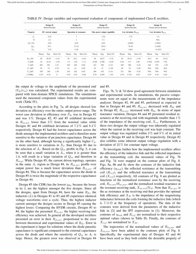
The four HVDR designs were implemented with a differentcombination of Ar and B to investigate which combinationof LC network components will deliver the best efficiencyand the required input resistance for the same Rdc. All theHVDR designs had the same MV , except Design #4, since asdiscussed in Section III-D, B had to be evaluated to yield aninput capacitance smaller than the tuning capacitance of Lrx.Ar in the CDR (Design #5) was selected to also result in acircuit with Rdc equal to the value for the other rectifiers.
For each design, the inductor (L) was implemented first.Based on its measured value the other passive componentswere chosen such that the initial selection of Ar and B,or just Ar for the CDR, was satisfied. In Table IV, theexperimental values of the capacitor in parallel with the diode,Cp for Designs #1 to #4 and C for Design #5, do notinclude the pn-junction capacitance of the diode (Cpn) andare hence the capacitance of the physical capacitors added tothe circuit which is equal to the design value. All inductorswere implemented with Micrometals iron powder cores forRF applications. Specifically, in Design #1 a T106-3 corewas used and in Designs #2 to #5 T106-2 cores were used.All capacitors were from the AVX high Q range. Componentimpedance measurements were made with a Keysight Tech-nologies impedance analyzer. All rectifiers utilised a singleWolfspeed SiC Schottky diode, the C3D10065A, which has10 A forward current capability and 650 V blocking voltagecapability.
B. Experimental Test Rig
To allow careful characterisation of rectifiers and to avoidthe need of an inductive link and its associated instrumentationfor testing the rectifier, a test rig was developed that reproducesIPT conditions in the tuned Rx coil when a rectifier is addedat the receiver. With this test rig calculation of the efficiency ofthe receiver (ηRx) and the input resistance of the rectifier undertest as seen from the output of the inverter, is possible withoutaffecting any other part of the IPT system. More informationabout the test rig and the calculation of the worst case error inthe experimental measurements can be found in Appendix B.Further implementation details for the test rig can be foundfrom our work in [35].
C. Experimental Results and Discussion
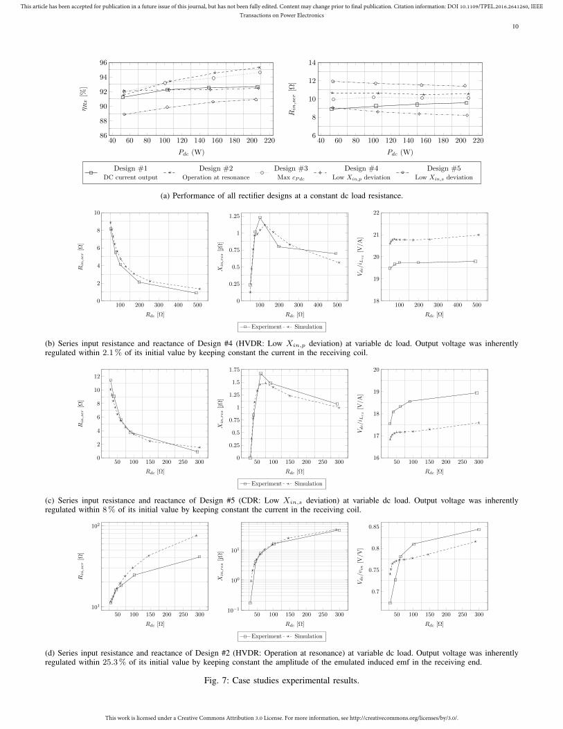
The five implemented rectifiers will now be compared withrespect to their efficiency and their effect on the inductive link.To ensure repeatability of results, a power sweep was per-formed in each experiment and measurements were recordedtwice, when the output power was increasing from minimumto maximum and when the output power was decreasing frommaximum to minimum. The results presented are the average.
The test rig enables measurement of the combinedimpedance of the receiving coil, external tuning capacitorand the rectifier under test. At resonance, this impedance isequal to the equivalent series input resistance of the rectifier,Rin,ser. In the current driven case, Rin,ser is equal to Rin,sand in the voltage driven case Rin,ser is equal to the seriestransformation of Rin,p. When the rectifier is designed toreflect the optimal load this Rin,ser value is equal to Rac,serindependent of series or parallel tuning (which is equal to10.6 Ω in this case study).
Fig. 7a presents the measured ηRx and Rin,ser for varyingpower (50 W to 200 W). Fig. 7b, Fig. 7c and Fig. 7d showthe results of the variable Rdc experiments for Designs #2,#4 and #5 over a dc load range between 10 % to 100 %.At every dc load step, the Rin,ser of the topology and theresidual reactance at the resonant tank (Xin,res) were cal-culated. Xin,res is the uncompensated reactance between thereactances of the Rx coil, the external tuning capacitor and theinput reactance of the rectifier. To examine the inherent voltageregulation feature, the ratio between the output dc voltageto the current in the receiving coil (Vdc/iin) was calculatedin Designs #4 and #5 and in Design #2 the ratio between
This work is licensed under a Creative Commons Attribution 3.0 License. For more information, see http://creativecommons.org/licenses/by/3.0/.
This article has been accepted for publication in a future issue of this journal, but has not been fully edited. Content may change prior to final publication. Citation information: DOI 10.1109/TPEL.2016.2641260, IEEETransactions on Power Electronics
9
TABLE IV: Design variables and experimental evaluation of components of implemented Class-E rectifiers.
Design #1 Design #2 Design #3 Design #4 Design #5Hybrid Rectifier Hybrid Rectifier Hybrid Rectifier Hybrid Rectifier Current Driven Rectifier
Property DC current output Operation at resonance Max power output capability Low deviation Xin,p Low deviation Xin,s
Ar 0.35 1 1.52 1.75 1.8
B 2.5 4 7.5 4 N/A
MV /MI 0.05 0.05 0.05 0.0683 0.3862
Qin 62.1 71.53 105.6 79.49 0.2403
Nin 3.73 5.26 8.28 4.601 −0.4573
Rdc [Ω]
L [µH]
C [pF]
Cs [pF]
Cp [pF]
f [MHz]
Theory Exp. Error [%]
29 30.58 −5.45
16 16.31 −1.94
265 261 1.51
76 74 0.72
189 186 1.59
6.78 6.78 0
Theory Exp. Error [%]
29 29.1 −0.34
1.8 1.82 −1.11
305 303 0.66
61 61 0.00
244 242 0.82
6.78 6.84 −0.88
Theory Exp. Error [%]
29 29.51 −1.76
0.529 0.596 −12.67
451 400 11.31
53 47 11.32
398 353 11.31
6.78 6.905 −1.84
Theory Exp. Error [%]
50 50.51 −1.02
0.53 0.5 5.66
339 360 −6.19
68 72 −5.88
271 280 −3.32
6.78 6.741 0.58
Theory Exp. Error [%]
33.5 30 10.45
0.302 0.278 7.95
564 575 −1.95
N/A N/A N/A
N/A N/A N/A
6.78 6.76 0.29
the output dc voltage to the amplitude of the presented emf(Vdc/vin) was calculated. The experimental results are com-pared with time-domain SPICE simulations. The simulationsused the measured component values from the experimentalwork (Table IV).
According to the plots in Fig. 7a, all designs showed lowdeviation in efficiency over the entire output power range. Theworst case deviation in efficiency over Pdc was in Design #2and was 4 %. Designs #2, #3 and #5 exhibited deviationsin Rin,ser lower than 3 % from the nominal value whileDesigns #1 and #4 exhibited deviations of 7.2 % and 9.4 %respectively. Design #1 had the lowest capacitance across thediode amongst the implemented rectifiers and is therefore moresensitive to the variation of pn junction capacitance. Design #4on the other hand, although having a significantly higher Cp,is more sensitive to variations in XC than Design #1 due tothe selection of Ar. Based on the Qin profile in Fig. 5, it canbe seen that a small variation in Ar, when it is greater than1.6, will result in a large variation of Qin and therefore inRin,p. While Design #5, the current driven topology, operatesin the same Ar region as Design #4, its Rin,ser profile overoutput power has a much lower deviation than Rin,ser ofDesign #4. This is because the capacitance across the diode inDesign #5 is twice the magnitude of the respective capacitancein Design #4.
Design #5 (the CDR) has the lowest ηRx because the lossesin its L are the highest amongst the five designs. Since allthe designs, apart from Design #4, have the same Rdc, theinductors (L) in Designs #1 to #3 and #5 experience identicalvoltage waveforms over a cycle. Thus, the highest inductorcurrent amongst the designs occurs in Design #5 causing thehighest losses. Comparing the HVDR circuits, Designs #1 to#4, the higher the presented Rin,ser the higher receiving endefficiency was achieved. In general all the developed rectifierspresented an error in their Rin,ser proportional to the errorbetween theoretical and experimental values of Rdc. Error inthe experiment is larger for solutions where the diode parasiticcapacitance is significant compared to the external capacitanceacross the diode and where the sensitivity of Qin to Ar islarge. Hence, the greatest error was observed in Designs #4
and #5.Figs. 7b, 7c & 7d show good agreement between simulation
and experimental results. In simulations, the passive compo-nents were set equal to the measurements of the impedanceanalyzer. Designs #2, #4 and #5, performed as expected inthat in Designs #4 and #5, Rin,ser decreased with Rdc andin Design #2, Rin,ser increased with Rdc. In terms of inputreactance variation, Designs #4 and #5 presented residual re-actances at the receiving end with magnitude smaller than 1 %of the impedance of the receiving coil, Xrx. Furthermore, inthese two designs the output voltage was inherently regulatedwhen the current in the receiving coil was kept constant. Theoutput voltage was regulated within 3 % and 8 % of its initialvalue in Design #4 and in Design #5 respectively. Design #2also exhibits some inherent output voltage regulation with adeviation of 25 % for constant input voltage.
To investigate further how the implemented rectifiers affectthe efficiency of the inductive link and the reflected impedanceat the transmitting coil, the measured values of Fig. 7band Fig. 7d were mapped on the contour plots of Fig. 8.Figs. 8a, 8b and 8c show the contours of the inductive linkefficiency (ηlink), the reflected resistance at the transmittingcoil (Rref ), and the reflected reactance at the transmittingcoil (Xref ) respectively. All contours of Fig. 8 are plotted asfunctions of the normalised resistance seen by the receivingcoil, Rin,ser/Rac,ser, and the normalised residual reactance atthe resonant receiving tank, Xin,res/XM . Note that Rac,ser isthe ac resistance at the receiving end that provides the optimallink efficiency and XM is the impedance of the magnetisinginductance between the coils forming the inductive link (whichis 7.11 Ω at the frequency of operation). The data of thecontours were derived from the parameters of the inductivelink in [2] and the IPT expressions in [1]. Moreover, thecontours of ηlink and Rref are normalised to their respectiveoptimal values (shown in Table II). Finally, the contours ofXref are normalised to XM .
The trajectories of the normalised values of Rin,ser andXin,res have been added to the contours plots of Fig. 8.Specifically, the experimental data of Designs #2 and #4have been used as they both exhibit the desirable property of
This work is licensed under a Creative Commons Attribution 3.0 License. For more information, see http://creativecommons.org/licenses/by/3.0/.
This article has been accepted for publication in a future issue of this journal, but has not been fully edited. Content may change prior to final publication. Citation information: DOI 10.1109/TPEL.2016.2641260, IEEETransactions on Power Electronics
10
40 60 80 100 120 140 160 180 200 22086
88
90
92
94
96
Pdc (W)
η Rx
[%]
40 60 80 100 120 140 160 180 200 2206
8
10
12
14
Pdc (W)
Rin,ser
[Ω]
Design #1DC current output
Design #2Operation at resonance
Design #3Max cPdc
Design #4Low Xin,p deviation
Design #5Low Xin,s deviation
(a) Performance of all rectifier designs at a constant dc load resistance.
100 200 300 400 5000
2
4
6
8
10
Rdc [Ω]
Rin,ser
[Ω]
100 200 300 400 5000
0.25
0.5
0.75
1
1.25
Rdc [Ω]
Xin,res
[jΩ
]
100 200 300 400 50018
19
20
21
22
Rdc [Ω]
Vdc/iL
rx
[V/A
]
Experiment Simulation
(b) Series input resistance and reactance of Design #4 (HVDR: Low Xin,p deviation) at variable dc load. Output voltage was inherentlyregulated within 2.1% of its initial value by keeping constant the current in the receiving coil.
50 100 150 200 250 3000
2
4
6
8
10
12
Rdc [Ω]
Rin,ser
[Ω]
50 100 150 200 250 3000
0.25
0.5
0.75
1
1.25
1.5
1.75
Rdc [Ω]
Xin,res
[jΩ
]
50 100 150 200 250 30016
17
18
19
20
Rdc [Ω]
Vdc/iL
rx
[V/A
]
Experiment Simulation
(c) Series input resistance and reactance of Design #5 (CDR: Low Xin,s deviation) at variable dc load. Output voltage was inherentlyregulated within 8% of its initial value by keeping constant the current in the receiving coil.
50 100 150 200 250 300101
102
Rdc [Ω]
Rin,ser
[Ω]
50 100 150 200 250 30010−1
100
101
Rdc [Ω]
Xin,res
[jΩ
]
50 100 150 200 250 300
0.7
0.75
0.8
0.85
Rdc [Ω]
Vdc/v in
[V/V
]
Experiment Simulation
(d) Series input resistance and reactance of Design #2 (HVDR: Operation at resonance) at variable dc load. Output voltage was inherentlyregulated within 25.3% of its initial value by keeping constant the amplitude of the emulated induced emf in the receiving end.
Fig. 7: Case studies experimental results.
This work is licensed under a Creative Commons Attribution 3.0 License. For more information, see http://creativecommons.org/licenses/by/3.0/.
This article has been accepted for publication in a future issue of this journal, but has not been fully edited. Content may change prior to final publication. Citation information: DOI 10.1109/TPEL.2016.2641260, IEEETransactions on Power Electronics
11
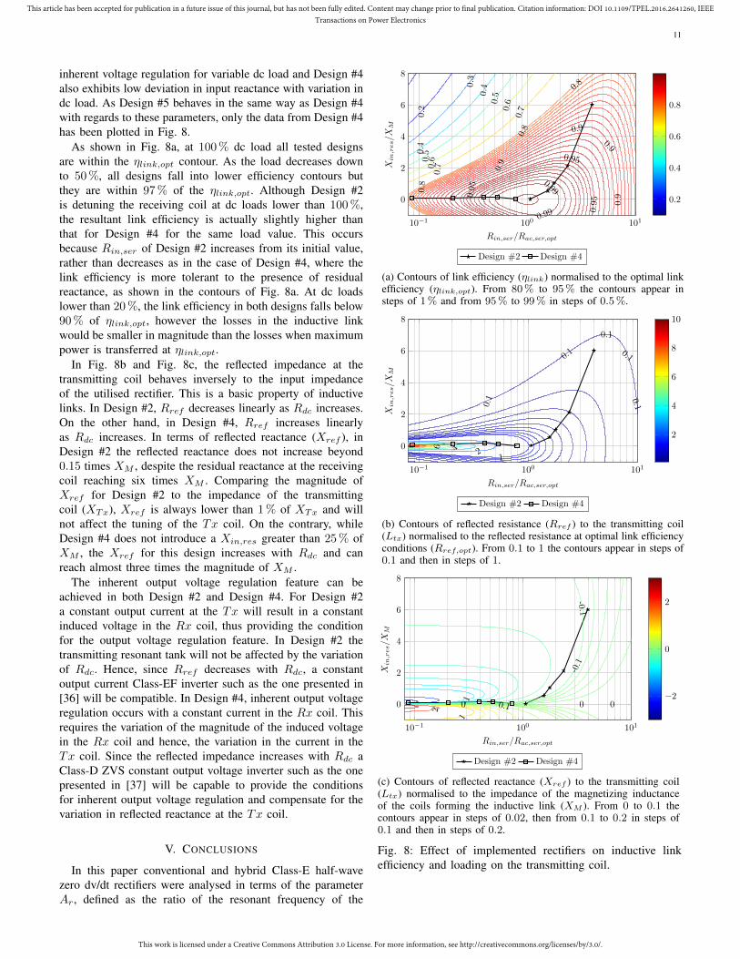
inherent voltage regulation for variable dc load and Design #4also exhibits low deviation in input reactance with variation indc load. As Design #5 behaves in the same way as Design #4with regards to these parameters, only the data from Design #4has been plotted in Fig. 8.
As shown in Fig. 8a, at 100 % dc load all tested designsare within the ηlink,opt contour. As the load decreases downto 50 %, all designs fall into lower efficiency contours butthey are within 97 % of the ηlink,opt. Although Design #2is detuning the receiving coil at dc loads lower than 100 %,the resultant link efficiency is actually slightly higher thanthat for Design #4 for the same load value. This occursbecause Rin,ser of Design #2 increases from its initial value,rather than decreases as in the case of Design #4, where thelink efficiency is more tolerant to the presence of residualreactance, as shown in the contours of Fig. 8a. At dc loadslower than 20 %, the link efficiency in both designs falls below90 % of ηlink,opt, however the losses in the inductive linkwould be smaller in magnitude than the losses when maximumpower is transferred at ηlink,opt.
In Fig. 8b and Fig. 8c, the reflected impedance at thetransmitting coil behaves inversely to the input impedanceof the utilised rectifier. This is a basic property of inductivelinks. In Design #2, Rref decreases linearly as Rdc increases.On the other hand, in Design #4, Rref increases linearlyas Rdc increases. In terms of reflected reactance (Xref ), inDesign #2 the reflected reactance does not increase beyond0.15 times XM , despite the residual reactance at the receivingcoil reaching six times XM . Comparing the magnitude ofXref for Design #2 to the impedance of the transmittingcoil (XTx), Xref is always lower than 1 % of XTx and willnot affect the tuning of the Tx coil. On the contrary, whileDesign #4 does not introduce a Xin,res greater than 25 % ofXM , the Xref for this design increases with Rdc and canreach almost three times the magnitude of XM .
The inherent output voltage regulation feature can beachieved in both Design #2 and Design #4. For Design #2a constant output current at the Tx will result in a constantinduced voltage in the Rx coil, thus providing the conditionfor the output voltage regulation feature. In Design #2 thetransmitting resonant tank will not be affected by the variationof Rdc. Hence, since Rref decreases with Rdc, a constantoutput current Class-EF inverter such as the one presented in[36] will be compatible. In Design #4, inherent output voltageregulation occurs with a constant current in the Rx coil. Thisrequires the variation of the magnitude of the induced voltagein the Rx coil and hence, the variation in the current in theTx coil. Since the reflected impedance increases with Rdc aClass-D ZVS constant output voltage inverter such as the onepresented in [37] will be capable to provide the conditionsfor inherent output voltage regulation and compensate for thevariation in reflected reactance at the Tx coil.
V. CONCLUSIONS
In this paper conventional and hybrid Class-E half-wavezero dv/dt rectifiers were analysed in terms of the parameterAr, defined as the ratio of the resonant frequency of the
10−1 100 101
0
2
4
6
8
0.2
0.3
0.4
0.4
0.5
0.5
0.6
0.6
0.7
0.7
0.8
0.8
0.8
0.9
0.90.9
0.90.95
0.95
0.95
0.99
0.99
Rin,ser/Rac,ser,opt
Xin,res/X
M
Design #2 Design #4
0.2
0.4
0.6
0.8
(a) Contours of link efficiency (ηlink) normalised to the optimal linkefficiency (ηlink,opt). From 80% to 95% the contours appear insteps of 1% and from 95% to 99% in steps of 0.5%.
10−1 100 101
0
2
4
6
8
0.1
0.1
0.1
0.1
0.1
1246
Rin,ser/Rac,ser,opt
Xin,res/X
M
Design #2 Design #4
2
4
6
8
10
(b) Contours of reflected resistance (Rref ) to the transmitting coil(Ltx) normalised to the reflected resistance at optimal link efficiencyconditions (Rref,opt). From 0.1 to 1 the contours appear in steps of0.1 and then in steps of 1.
10−1 100 101
0
2
4
6
8
-1
-0.1
-0.1
0 0 00.1
1
2
Rin,ser/Rac,ser,opt
Xin,res/X
M
Design #2 Design #4
−2
0
2
(c) Contours of reflected reactance (Xref ) to the transmitting coil(Ltx) normalised to the impedance of the magnetizing inductanceof the coils forming the inductive link (XM ). From 0 to 0.1 thecontours appear in steps of 0.02, then from 0.1 to 0.2 in steps of0.1 and then in steps of 0.2.
Fig. 8: Effect of implemented rectifiers on inductive linkefficiency and loading on the transmitting coil.

This work is licensed under a Creative Commons Attribution 3.0 License. For more information, see http://creativecommons.org/licenses/by/3.0/.
This article has been accepted for publication in a future issue of this journal, but has not been fully edited. Content may change prior to final publication. Citation information: DOI 10.1109/TPEL.2016.2641260, IEEETransactions on Power Electronics
12
utilised LC network to the operating frequency. The resultsof this analysis were illustrated in a way that designers areable to observe the variations in rectifier behavior over Ar andchoose the best suited topology based on the requirements ofthe application. Based on the analytical results the followingconclusions can be made about half-wave Class-E rectifiersoperating with a duty cycle equal or lower than 50 % whendesigned for IPT:
• The voltage driven Class-E rectifier with a series inductorwill always require an inductor of larger impedance thanthe impedance of the receiving coil to allow the inputresistance required by optimal link efficiency conditionsto be presented. Therefore, the implementation of theseries inductor will always be a challenge when high Q,high impedance coils are forming the link.
• The voltage driven Class-E rectifier with a series ca-pacitor does not absorb the parasitic capacitance of thediode in its LC network and its operation will be heaviliyaffected when the pn junction capacitance is in the sameorder of magnitude as the series capacitor.
• There are specific regions of Ar where the behaviorof the input resistance of the rectifiers is consistentwith duty cycle variations. When Ar is unity the seriesinput resistance of the rectifiers, whether being voltageor current driven, increases as the output dc resistanceincreases. On the other hand, when Ar is greater than1.5, the series input resistance of the rectifiers decreasesas the dc resistance increases.
• The current driven topology, the voltage driven topologywith a series capacitor and the hybrid topology, exhibita low deviation in their input reactance as the output dcresistance increases, when designed with an Ar between1.75 and 2. In particular a deviation by less than 13 %is observed in the input reactance of the current driventopology and a deviation by less than 5 % is observed inthe input reactance of the latter two rectifier topologies.
The case studies in this work were focused on making theuse of Class-E rectifiers feasible and effective in IPT systems.Furthermore, the experiments aimed to investigate the effectof passives on the performances of the hybrid rectifier and toevaluate the behavior of input resistance and input reactance ofthe hybrid and current driven rectifiers. A test rig was devel-oped that emulates IPT conditions and properly characterisesrectifiers without the need of an inductive link. Based on theexperimental results the following conclusions can be made:
• The best efficiency was recorded in the hybrid topologywhen designed to operate at a unity Ar.
• The sensitivity of the implemented rectifiers on thediode’s pn junction capacitance becomes higher when Aris smaller than 0.4 and greater than 1.6. In the formerregion, the external capacitor across the diode is lowerthan the resultant capacitance in any other Ar regionwhen the rectifier is designed to present the same inputresistance while having the same dc load. In the latterregion, a small variation in Ar will result in a much largervariation in the input resistance of the topology.
• The hybrid and current driven Class-E rectifiers, when
designed at Ar between 1.75 to 2 can provide inherentoutput voltage regulation as their dc load decreases from100 % to 10 %. This feature is feasible by keeping thecurrent in the receiving coil constant. The achieved reg-ulation was within 3 % and 8 % of the nominal outputvoltage for the hybrid and the current driven rectifierrespectively.
In summary, the hybrid rectifier has been shown to be agood choice for weakly coupled inductive links as it canhave a power robust operation and match any dc load to thedesirable ac resistance while exhibiting any of the properties ofthe conventional Class-E half-wave zero dv/dt rectifiers. Thisincludes low loss inductor realisation, low deviation in inputreactance and inherent output voltage regulation.
APPENDIX AEQUATIONS AND GENERAL DERIVATION METHOD OF
CLASS-E RECTIFIER DESIGN VARIABLES
The input sources were assumed sinusoidal and were ex-pressed by:
vin(θ) =VdcMV
sin(θ + φ), (11)
in the voltage driven topologies, and:
iin(θ) =IdcMI
sin(θ + φ), (12)
in the current driven topology. In both (11) and (12) θ is theproduct of ω and time, t, and φ is the phase of the input sourcewhen the diode turns OFF. The following definitions were alsoused:
iC(θ) =
(1
XC
)d
dθ[vD(θ)] , (13)
vL(θ) = XLd
dθ[iL(θ)] , (14)
−Vdc =1
2π
∫ ψ
0
vD(θ)dθ, (15)
Idc =1
2π
∫ 2π
ψ
iD(θ)dθ, (16)
where (15) and (16) are derived by applying Kirchoff’s voltageand current laws respectively. Variable ψ is the interval inwhich the diode is reverse biased:
ψ = 2π(1 − dr). (17)
From (15) and (16) the loaded quality factor as a function ofψ, and hence duty cycle, is given by:
Qr = −( ∫ ψ
0vD(θ)dθ∫ 2π
ψiD(θ)dθ
)(1
X
). (18)
In order for the topologies to achieve low dvD/dt at turn OFFthe following conditions must also be met:
vD(0) = vD(ψ) =d
dθ[vD(0)] = 0, (19)
iD(2π) = 0, (20)
iC(ψ−) = iD(ψ+). (21)
This work is licensed under a Creative Commons Attribution 3.0 License. For more information, see http://creativecommons.org/licenses/by/3.0/.
This article has been accepted for publication in a future issue of this journal, but has not been fully edited. Content may change prior to final publication. Citation information: DOI 10.1109/TPEL.2016.2641260, IEEETransactions on Power Electronics
13
Finally the following expressions have to be used for deriv-ing the input reactance of the rectifiers at the frequency ofoperation:
iin,1 =1
π
∫ 2π
0
ivin(θ) cos(θ + φ)dθ, (22)
vin,1 =1
π
∫ 2π
0
viin(θ) cos(θ + φ)dθ, (23)
where iin,1 is the first harmonic of the current ivin , which isdrawn from the input source in the voltage driven rectifiersand vin,1 is the first harmonic of the voltage viin across theinput source in the CDR.
The equations of the design variables of the examinedrectifiers are presented in Table V to Table VI. It shouldbe noted that for the CDR (Fig. 2b) and the series-C VDR(Fig. 2c), there are different equations describing variablesφ and Qr, although their profiles over duty cycle and ratioAr have the same evaluation. Furthermore, in the HVDR(Fig. 2a), variables φ and Qr are independent of variable Band are therefore expressed by the equations of the respectivevariables in the series-C VDR. The process of deriving thedesign variables as functions of duty cycle and ratio Ar canbe found in [26] for operation at resonance and in [30] foroperation around resonance.
APPENDIX BDESCRIPTION OF TESTING APPARATUS
Characterising a rectifier in terms of input resistance andefficiency while integrated in a multi-MHz IPT system is nota trivial task. Calculation of input power to the rectifier willbe required and therefore the voltage across the receivingcoil, vLrx , and the current through it have to be measured. Inthis frequency range the capacitance introduced by a voltageprobe is not negligible and can affect the circuit under test.Therefore, measuring the voltage across Lrx while operating ina complete IPT system, will detune the receiving end and leadto wrong assumptions about the effect of the rectifier on the in-ductive link. Furthermore, while instrumentation via capacitivedivision could make the presence of a voltage probe intrinsiccapacitance insignificant, the input power measurement willstill be of great uncertainty beause the phase between vLrx
and the current input to the rectifier will be nearly ninetydegrees. Therefore, small errors in phase will cause largeerrors in the ac power measurement. Hence, a test rig forrectifier characterisation was developed that overcomes thesechallenges by taking the measurements separately from theinductive link.
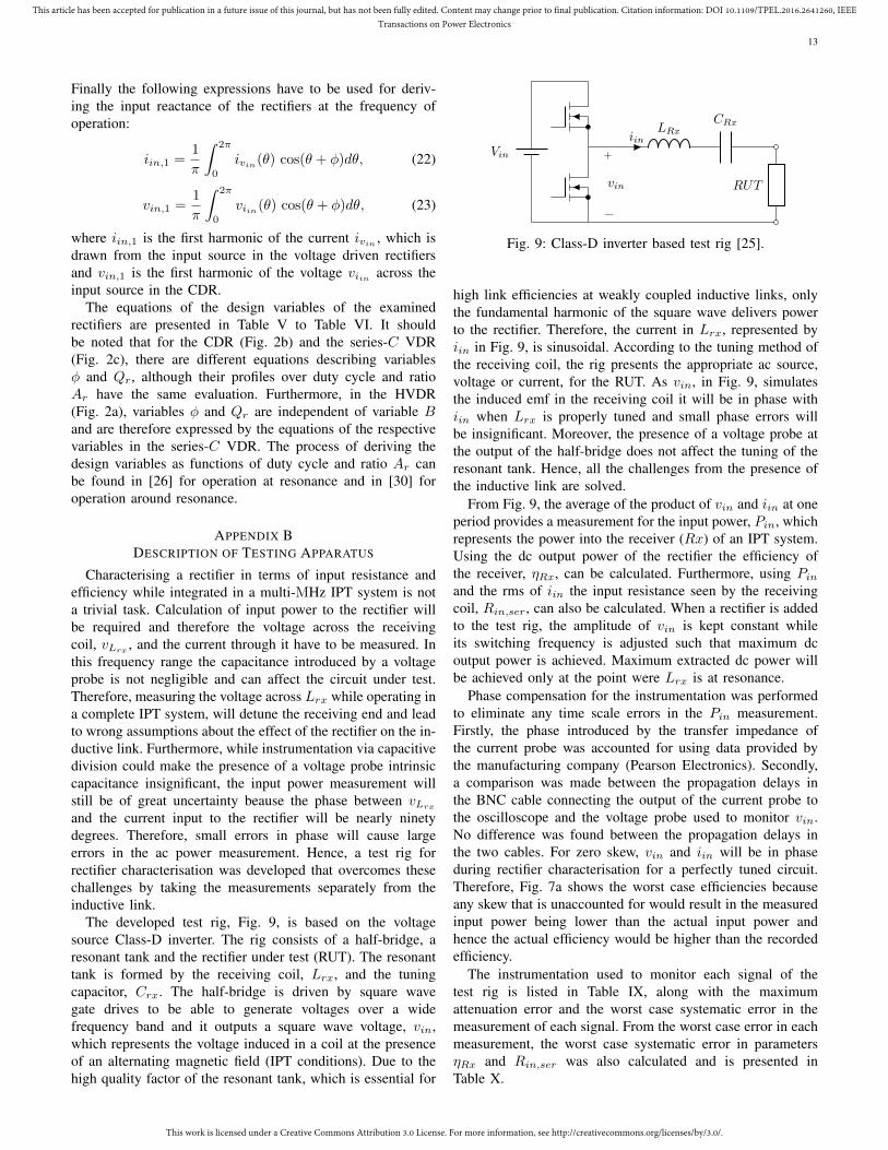
The developed test rig, Fig. 9, is based on the voltagesource Class-D inverter. The rig consists of a half-bridge, aresonant tank and the rectifier under test (RUT). The resonanttank is formed by the receiving coil, Lrx, and the tuningcapacitor, Crx. The half-bridge is driven by square wavegate drives to be able to generate voltages over a widefrequency band and it outputs a square wave voltage, vin,which represents the voltage induced in a coil at the presenceof an alternating magnetic field (IPT conditions). Due to thehigh quality factor of the resonant tank, which is essential for
Vin
LRxiin
CRx
RUT
+
−
vin
Fig. 9: Class-D inverter based test rig [25].
high link efficiencies at weakly coupled inductive links, onlythe fundamental harmonic of the square wave delivers powerto the rectifier. Therefore, the current in Lrx, represented byiin in Fig. 9, is sinusoidal. According to the tuning method ofthe receiving coil, the rig presents the appropriate ac source,voltage or current, for the RUT. As vin, in Fig. 9, simulatesthe induced emf in the receiving coil it will be in phase withiin when Lrx is properly tuned and small phase errors willbe insignificant. Moreover, the presence of a voltage probe atthe output of the half-bridge does not affect the tuning of theresonant tank. Hence, all the challenges from the presence ofthe inductive link are solved.
From Fig. 9, the average of the product of vin and iin at oneperiod provides a measurement for the input power, Pin, whichrepresents the power into the receiver (Rx) of an IPT system.Using the dc output power of the rectifier the efficiency ofthe receiver, ηRx, can be calculated. Furthermore, using Pinand the rms of iin the input resistance seen by the receivingcoil, Rin,ser, can also be calculated. When a rectifier is addedto the test rig, the amplitude of vin is kept constant whileits switching frequency is adjusted such that maximum dcoutput power is achieved. Maximum extracted dc power willbe achieved only at the point were Lrx is at resonance.
Phase compensation for the instrumentation was performedto eliminate any time scale errors in the Pin measurement.Firstly, the phase introduced by the transfer impedance ofthe current probe was accounted for using data provided bythe manufacturing company (Pearson Electronics). Secondly,a comparison was made between the propagation delays inthe BNC cable connecting the output of the current probe tothe oscilloscope and the voltage probe used to monitor vin.No difference was found between the propagation delays inthe two cables. For zero skew, vin and iin will be in phaseduring rectifier characterisation for a perfectly tuned circuit.Therefore, Fig. 7a shows the worst case efficiencies becauseany skew that is unaccounted for would result in the measuredinput power being lower than the actual input power andhence the actual efficiency would be higher than the recordedefficiency.
The instrumentation used to monitor each signal of thetest rig is listed in Table IX, along with the maximumattenuation error and the worst case systematic error in themeasurement of each signal. From the worst case error in eachmeasurement, the worst case systematic error in parametersηRx and Rin,ser was also calculated and is presented inTable X.

This work is licensed under a Creative Commons Attribution 3.0 License. For more information, see http://creativecommons.org/licenses/by/3.0/.
This article has been accepted for publication in a future issue of this journal, but has not been fully edited. Content may change prior to final publication. Citation information: DOI 10.1109/TPEL.2016.2641260, IEEETransactions on Power Electronics
14
TABLE V: Design variables of current driven rectifier (Fig. 2b).
Operating away from resonance, Ar 6=1,
tanφ = −Ar [(cos(Ar ψ)− cosψ) (sin(Ar ψ) +Ar (2π − ψ))− (sin(Ar ψ)−Ar sinψ) (cos(Ar ψ)− 1)]/
(cos(Ar ψ)− 1) (Ar2 (cosψ − 1) + 2 sin((Ar ψ)/2)2)− (sin(Ar ψ)−Ar sinψ) [sin(Ar ψ) +Ar (2π − ψ)].(24)
Qr =− 4π [sin(Ar ψ) sinφ+Ar cos(φ+ ψ)−Ar cos(Ar ψ) cosφ]/−Ar3 [2 cos(φ+ ψ) (1− cos(Ar ψ))
+ cosφ (2 (cos(Ar ψ)− 1) + cosψ (2π − ψ)2 − cos(Ar ψ) (ψ − 2π)2) + sinφ (2π − ψ) ((ψ − 2π) sinψ
+ 2 (cos(Ar ψ)− 1))]− 2Ar (cos(Ar ψ)− 1) (cos(φ+ ψ)− cosφ− 2π sinφ+ ψ sinφ)
−Ar2 sin(Ar ψ) sinφ (2π − ψ)2.
(25)
MI = [sin(Ar ψ) sinφ+Ar cos(φ+ ψ)−Ar cos(Ar ψ) cosφ]/[ArQ (Ar2 − 1) (cos(Ar ψ)− 1)]. (26)
Nin =
− ψ/[2π (Ar2 − 1)]− [(2 sin(Ar ψ) (1−Ar2)) (cosφ)2 + sinψ (2Ar (1−Ar2)) (sinφ)2 − 2 sin(Ar ψ)] cosψ
+ [Ar sin(2φ)(1−Ar2)] (sinψ)2 + [Ar sin(2ψ) (Ar2 − 1)]/2 + sinψ [2Ar cos(Ar ψ)
− sin(2φ) sin(Ar ψ) (1−Ar2)]/[2Ar π (Ar2 − 1)2]−KQ 2 cos(Ar ψ) sin(φ+ ψ)− 2Ar sin(Ar ψ) cos(φ+ ψ)
+ 2 sin(φ+ ψ) (Ar2 − 1)− 2Ar2 sinφ/[2π (Ar2 − 1)].
(27)
Operating at resonance, Ar =1.
tanφ = −[ψ sinψ (ψ − 2π) + (cosψ − 1) (ψ + sinψ)]/[(cosψ)2 + (ψ2 − 2π ψ − 4) cosψ + (2π − 2ψ) sinψ + 3]. (28)
Qr =4π [ψ sin(φ+ ψ)− sinφ sinψ]/4 cos(φ+ ψ) + cosφ (4 (cosψ − 1) + ψ sinψ (ψ − 2π)2)− 4 cos(φ+ ψ) cosψ
+ sinφ (2π − ψ) [4 (cosψ − 1) + (2π − ψ) (ψ cosψ − sinψ)].(29)
MI = [ψ sin(φ+ ψ)− sinφ sinψ]/[2Qr (cosψ − 1)]. (30)
Nin =[2ψ + 2 sin(2φ) + sin(2ψ)− 2 sin(2 (φ+ ψ))− 4ψ (sinφ)2 − 4ψ sin(φ+ ψ)2]/[16π]
+ [MI Qr (sin(φ+ 2ψ)/2− 2 sin(φ+ ψ) + (3 sinφ)/2 + ψ cosφ)]/[2π].(31)
TABLE VI: Design variables of voltage driven rectifier with series inductor (Fig. 2d).
Operating away from resonance, Ar 6=1.
tan(φ+ π) =
4 sin((Ar ψ)/2)2 (Ar2 sin(ψ/2)2 − 1) +Ar sinψ (sin(Ar ψ)−Ar (2π − ψ))−Ar sin(Ar ψ) (2π − ψ)/Ar [(1− cosψ) sin(Ar ψ) + (Ar (2π − ψ + sinψ)) cos(Ar ψ)−Ar (sinψ + cosψ (2π − ψ))].
(32)
MV = Ar [cosφ (sin(Ar ψ)−Ar sinψ) +Ar sinφ (cos(Ar ψ)− cosψ)]/[(Ar2 − 1) (cos(Ar ψ)− 1)]. (33)
Qr = 2 (Ar2 − 1) (Ar ψ − sin(Ar ψ))MV +Ar2 (sin(Ar ψ)−Ar sinψ) sinφ+Ar (2 sin((Ar ψ)/2)2
+Ar2 (cosψ − 1)) cosφ/Ar (Ar2 − 1) (2 sin(φ+ ψ)− 2 sinφ+ 2 cosφ (2π − ψ) +MV (ψ − 2π)2).(34)
Nin = [4π Ar (Ar2 − 1)2]/[4π − 2ψ + 2 sin(2φ+ ψ)− sin(2φ)− sin(2φ+ 2ψ) + 2 sinψ − 4MV (cos(φ+ ψ)
− cosφ− sin(φ+ ψ)(2π − ψ))]Ar5 + [2ψ − 8π + 2 sin(2φ+ ψ) (cos(Ar ψ)− 2) + sin(2φ) + sin(2φ+ 2ψ)
− 2 sinψ (cos(Ar ψ) + 2)−MV (4 cos(φ+ ψ) (cos(Ar ψ)− 2) + 4 cosφ+ 8 sin(φ+ ψ) (2π − ψ))]Ar3
+ 4 sin(Ar ψ) [(cosψ −MV sin(φ+ ψ))Ar2 +MV sin(φ+ ψ)] + [2 (2π − (sin(2φ+ ψ) + sinψ) (cos(Ar ψ)− 1))
+ 4MV (cos(φ+ ψ) (cos(Ar ψ)− 1) + sin(φ+ ψ) (2π − ψ))]Ar.
(35)
Operating at resonance, Ar =1 (Derived expressions same as in [26]).
tanφ = [2 cosψ (cosψ + ψ (ψ − 2π)− 4) + 4 sinψ (π − ψ) + 6]/[sin(2ψ) + 2 ((ψ − 2π)ψ − 1) sinψ + 2ψ (cosψ − 1)]. (36)
MV = [ψ cos(φ+ ψ)− cosφ sinψ]/[2 (cosψ − 1)]. (37)
Qr =[cos(φ− ψ) + 3 cos(φ+ ψ)− 4 cosφ+ 2ψ sin(φ+ ψ) + 4MV (ψ − sinψ)]/
[4 sin(φ+ ψ)− 4 sinφ+ 4 cosφ (2π − ψ) + 2MV (ψ − 2π)2].(38)
Nin = −16π/[(4 cos(φ+ 2ψ) + 16 cos(φ+ ψ)− 20 cosφ+ 16 (ψ − 2π) sin(φ+ ψ) + 8ψ sinφ)MV + 6ψ − 16π)
− 8 sin(2φ+ ψ + 4 sin(2φ) + sin(2ψ) + 4 sin(2φ+ 2ψ)− 8 sinψ + 2ψ cos(2φ)− 2ψ cos(2φ+ 2ψ)].(39)

This work is licensed under a Creative Commons Attribution 3.0 License. For more information, see http://creativecommons.org/licenses/by/3.0/.
This article has been accepted for publication in a future issue of this journal, but has not been fully edited. Content may change prior to final publication. Citation information: DOI 10.1109/TPEL.2016.2641260, IEEETransactions on Power Electronics
15
TABLE VII: Design variables of voltage driven rectifier with series capacitor (Fig. 2c).
Operating away from resonance, Ar 6=1.
tanφ =
− [(cos(Ar ψ)− 1) (Ar2 (cosψ − 1) + 2 sin((Ar ψ)/2)2)− (sin(Ar ψ)−Ar sinψ) (sin(Ar ψ) +Ar (2π − ψ))]/
[Ar (sin(Ar ψ)−Ar sinψ) (cos(Ar ψ)− 1)−Ar (cos(Ar ψ)− cosψ) (sin(Ar ψ) +Ar (2π − ψ))].
(40)
MV = (sin(Ar ψ) cosφ−Ar (sin(φ+ ψ)− cos(Ar ψ) sinφ))/(Ar (Ar2 − 1) (cos(Ar ψ)− 1)). (41)
Qr =
[4 sin((Ar ψ)/2)2 cosφ+ 2Ar sin(Ar ψ) (MV + sinφ)− 2Ar2 (cosφ− cos(φ+ ψ) +MV ψ)− 2Ar
3MV (sin(Ar ψ)
−Ar ψ)]/[Ar4 (2 sin(φ+ ψ)− 2 sinφ (sinψ (2π − ψ) + 1) +MV (2π − ψ)2 + 2 cosφ cosψ (2π − ψ))
−Ar2 (2 sin(φ+ ψ)− 2 sinφ+ 2 cos(Ar ψ) cosφ (2π − ψ))−Ar
6MV (2π − ψ)2 − 2Ar5MV sin(Ar ψ) (2π − ψ)
+ 2Ar3 sin(Ar ψ) (MV + sinφ) (2π − ψ)].
(42)
Nin =
4π (Ar2 − 1)2/[4π +MV (4 (cos(Ar ψ) cos(φ+ ψ)− cosφ))]Ar
4 +MV [4 sin(Ar ψ) sin(φ+ ψ)]Ar3 + [2ψ − 8π
+ sin(2φ) + 2 cos(Ar ψ) sinψ + sin(2φ+ 2ψ)−MV (4 (cos(Ar ψ) cos(φ+ ψ)− cosφ))
− 2 sin(2φ+ ψ) cos(Ar ψ)]Ar2 − [MV (4 sin(Ar ψ) sin(φ+ ψ)) + 4 sin(Ar ψ) cosψ]Ar + 2 (2π − ψ)− sin(2φ)
+ 2 cos(Ar ψ) sinψ − sin(2φ+ 2ψ) + 2 sin(2φ+ ψ) cos(Ar ψ).
(43)
Operating at resonance, Ar =1 (Derived expressions same as in [33]).
tanφ = [2 (π − ψ) sinψ + (cosψ)2 + ((ψ − 2π)ψ − 4) cosψ + 3]/[(cosψ − 1 + (ψ − 2π)ψ) sinψ + ψ (cosψ − 1)]. (44)
MV = −[cosφ sinψ − ψ cos(φ+ ψ)]/(2 cosψ − 2). (45)
Qr =
4 [(sinψ − ψ)MV + cosφ]− 2 [cos(φ+ ψ) + cosφ cosψ + ψ sin(φ+ ψ)]/(4 (2π − ψ) sinψ
+ 2 (ψ − 2π)2)MV + 4 sinφ+ 3 cos(φ+ ψ) (ψ − 2π) + (ψ − 2π) cos(φ− ψ) + 2 sin(φ+ ψ) [(ψ − 2π)ψ − 2].(46)
Nin = (16π)/[4MV (cos(φ+ 2ψ)− cosφ+ 2ψ sinφ) + 16π + sin(2ψ) + 2ψ (cos(2φ)− cos(2φ+ 2ψ)− 1)]. (47)
TABLE VIII: Design variables of hybrid rectifier (Fig. 2a).
Operating away from resonance, Ar 6=1
tanφ = eq(40) MV = eq(41)/[B + 1] Qr = eq(42)
Nin =
(4π (Ar2 − 1)2 (B + 1)2)/[cosφ (4 cosψ (1−Ar2) (cos(Ar ψ)− cosψ)) + 4ArMV (Ar2 − 1) (sin(Ar ψ) cosψ
−Ar cos(Ar ψ) sinψ) (B + 1)] sinφ+ 4π (B + 1)− 2ψ + sin(2ψ) +Ar4 (4π (B + 1))
− [4 sinψ (Ar2 − 1) (cos(Ar ψ)− cosψ)] cosφ2 + cosφ [4ArMV (Ar2 − 1) (B + 1) (sin(Ar ψ) sinψ
+Ar (cos(Ar ψ) cosψ − 1))]−Ar2 (8π (B + 1)− 2ψ + sin(2ψ)− 4 cos(Ar ψ) sinψ)− 4Ar sin(Ar ψ) cosψ.
(48)
Operating at resonance, Ar =1
tanφ = eq(44) MV = eq(45)/[B + 1] Qr = eq(46)
Nin = 16π (B + 1)2/
[8MV ψ sinφ+ 16π + 4MV (cos(φ+ 2ψ)− cosφ)] (B + 1) + sin(2ψ) + 2ψ (cos(2φ)− cos(2φ+ 2ψ)− 1).(49)
TABLE IX: Worst case errors in test rig measurements.
MeasuredQuantity
ProbePart Number Attenuation Attenuation
ErrorMeasurement
Error
vin PPE 6kV 1000:1 2 % 1.96 %
iin 6585 CM 1:1 N/A 1 %∗
Vdc N2891A 100:1 2 % 1.94 %
Idc N2783A 10:1 1 % 0.892 %
∗Error in current to voltage transformation.
TABLE X: Worst case errors in receiving end efficiency (ηRx)and rectifier input series resistance (Rin,ser).
Calculated Quantity Positive Error Negative Error
ηRx 5.97 % 5.63 %
Rin,ser 2.99 % 2.93 %
ACKNOWLEDGMENTS
The authors would like to acknowledge Dr. Samer Aldhaherand Mr. Juan Manuel Arteaga Saenz for the useful discussions

This work is licensed under a Creative Commons Attribution 3.0 License. For more information, see http://creativecommons.org/licenses/by/3.0/.
This article has been accepted for publication in a future issue of this journal, but has not been fully edited. Content may change prior to final publication. Citation information: DOI 10.1109/TPEL.2016.2641260, IEEETransactions on Power Electronics
16
on the structure and presentation of this work. Furthermore,the authors would like to acknowledge the following fundingsources: EPSRC/EDF Case award number: 1401488, EPSRCUK-China: Interface and Network Infrastructure to SupportEV Participation in Smart Grids; grant ref: EP/L00089X/1,EPSRC Underpinning Power Electronics 2012: ComponentsTheme; grant ref: EP/K034804/1.
REFERENCES
[1] K. van Schuylenbergh and R. Puers, Inductive Powering: Basic Theoryand Application to Biomedical Systems. Springer, 2009.
[2] M. Pinuela, D. C. Yates, S. Lucyszyn, and P. D. Mitcheson, “MaximizingDC-to-load efficiency for inductive power transfer,” IEEE Trans. PowerElectron., vol. 28, no. 5, pp. 2437–2447, 2013.
[3] C. H. Kwan, G. Kkelis, S. Aldhaher, J. Lawson, D. C. Yates, P. C.-K. Luk, and P. D. Mitcheson, “Link efficiency-led design of mid-rangeinductive power transfer systems,” in IEEE PELS Workshop on EmergingTechnologies: Wireless Power (WoW), 2015. IEEE, 2015, pp. 1–7.
[4] M. K. Kazimierczuk and J. Jozwik, “Class-E zero-voltage-switchingand zero-current-switching rectifiers,” IEEE Trans. Circuits Syst. I, Reg.Papers, vol. 37, no. 3, pp. 436–444, 1990.
[5] S. Birca-Galateanu and A. Ivascu, “Class-E low dv/dt and low di/dtrectifiers: energy transfer, comparison, compact relationships,” IEEETrans. Circuits Syst. I, Fundam. Theory Appl. (19932003), vol. 48, no. 9,pp. 1065–1074, Sep 2001.
[6] W. Nitz, W. Bowman, F. Dickens, F. Magalhaes, W. Strauss, W. Suiter,and N. Ziesse, “A new family of resonant rectifier circuits for high fre-quency DC-DC converter applications,” in Third Annual IEEE AppliedPower Electronics Conference and Exposition (APEC), 1988. IEEE,1988, pp. 12–22.
[7] W. Cai, Z. Zhang, X. Ren, and Y.-F. Liu, “A 30-MHz isolated push-pullVHF resonant converter,” in Twenty-Ninth Annual IEEE Applied PowerElectronics Conference and Exposition (APEC), 2014. IEEE, 2014, pp.1456–1460.
[8] J. M. Rivas, D. Jackson, O. Leitermann, A. D. Sagneri, Y. Han, andD. J. Perreault, “Design considerations for very high frequency dc-dc converters,” in 37th IEEE Power Electronics Specialists Conference,2006. PESC’06. IEEE, 2006, pp. 1–11.
[9] Y. Han, O. Leitermann, D. Jackson, J. M. Rivas, D. J. Perreaultet al., “Resistance compression networks for radio-frequency powerconversion,” IEEE Trans. Power Electron., vol. 22, no. 1, pp. 41–53,2007.
[10] J. M. Rivas, O. Leitermann, Y. Han, and D. J. Perreault, “A very highfrequency DC–DC converter based on a class resonant inverter,” IEEETrans. Power Electron., vol. 26, no. 10, pp. 2980–2992, 2011.
[11] J. S. Glaser and J. M. Rivas, “A 500 W push-pull dc-dc power converterwith a 30 MHz switching frequency,” in Twenty-Fifth Annual IEEEApplied Power Electronics Conference and Exposition (APEC), 2010.IEEE, 2010, pp. 654–661.
[12] Z. Zhang, J. Lin, Y. Zhou, and X. Ren, “Analysis and Decoupling Designof a 30 MHz Resonant SEPIC Converter,” IEEE Trans. Power Electron.,vol. 31, no. 6, pp. 4536–4548, June 2016.
[13] K. H. Lee, E. Chung, G. S. Seo, and J. I. Ha, “Design of GaN transistor-based class E DC-DC converter with resonant rectifier circuit,” inIEEE 3rd Workshop on Wide Bandgap Power Devices and Applications(WiPDA), 2015, Nov 2015, pp. 275–280.
[14] S. Aldhaher, D. C. Yates, and P. D. Mitcheson, “Design and Develop-ment of a Class EF 2 Inverter and Rectifier for Multi-megahertz WirelessPower Transfer Systems,” IEEE Trans. Power Electron., vol. PP, no. 99,pp. 1–1, 2016.
[15] G. Kkelis, J. Lawson, D. Yates, M. Pinuela, and P. Mitcheson, “Inte-gration of a Class-E low DV/DT rectifer in a wireless power transfersystem,” in Wireless Power Transfer Conference (WPTC), 2014 IEEE,May 2014, pp. 72–75.
[16] S. Aldhaher, P. C.-K. Luk, K. El Khamlichi Drissi, and J. F. Whidborne,“High-Input-Voltage High-Frequency Class E Rectifiers for ResonantInductive Links,” IEEE Trans. Power Electron., vol. 30, no. 3, pp. 1328–1335, 2015.
[17] M. K. Kazimierczuk, “Analysis of Class-E zero-voltage-switching rec-tifier,” IEEE Trans. Circuits Syst. I, Reg. Papers, vol. 37, no. 6, pp.747–755, Jun 1990.
[18] R. C. Pilawa-Podgurski, A. D. Sagneri, J. M. Rivas, D. Anderson, D. J.Perreault et al., “Very-high-frequency resonant boost converters,” IEEETrans. Power Electron., vol. 24, no. 6, pp. 1654–1665, 2009.
[19] W. Liang, J. Glaser, and J. Rivas, “13.56 MHz High Density DC-DCConverter With PCB Inductors,” IEEE Trans. Power Electron., vol. 30,no. 8, pp. 4291–4301, Aug 2015.
[20] J. Santiago-Gonzalez, K. M. Elbaggari, K. K. Afridi, D. J. Perreaultet al., “Design of Class E Resonant Rectifiers and Diode Evaluation forVHF Power Conversion,” IEEE Trans. Power Electron., vol. 30, no. 9,pp. 4960–4972, 2015.
[21] K. Inoue, T. Nagashima, X. Wei, and H. Sekiya, “Design of high-efficiency inductive-coupled wireless power transfer system with class-DE transmitter and class-E rectifier,” in Industrial Electronics Society,IECON 2013 - 39th Annual Conference of the IEEE, Nov 2013, pp.613–618.
[22] M. Liu, M. Fu, and C. Ma, “Parameter Design for A 6.78-MHz WirelessPower Transfer System Based on Analytical Derivation of Class ECurrent-Driven Rectifier,” IEEE Trans. Power Electron., vol. PP, no. 99,pp. 1–1, 2015.
[23] M. K. Kazimierczuk and J. Jozwik, “Class E zero-voltage-switchingrectifier with a series capacitor,” IEEE Transactions on Circuits andSystems, vol. 36, no. 6, pp. 926–928, 1989.
[24] M. Kazimierczuk and W. Szaraniec, “Analysis of a Class-E rectifier witha series capacitor,” IEE Proceedings G (Circuits, Devices and Systems),vol. 139, no. 3, Jun 1992.
[25] G. Kkelis, D. C. Yates, and P. D. Mitcheson, “Comparison of cur-rent driven Class-D and Class-E half-wave rectifiers for 6.78 MHzhigh power IPT applications,” in Wireless Power Transfer Conference(WPTC), 2015 IEEE. IEEE, 2015, pp. 1–4.
[26] A. Ivascu, M. Kazimierczuk, and S. Birca-Galateanu, “Class-E resonantlow dv/dt rectifier,” IEEE Trans. Circuits Syst. I, Fundam. Theory Appl.(19932003), vol. 39, no. 8, pp. 604–613, Aug 1992.
[27] M. Kazimierczuk, B. Tomescu, and A. Ivascu, “Class-E resonant rectifierwith a series capacitor,” IEEE Trans. Circuits Syst. I, Fundam. TheoryAppl. (1993-2003), vol. 41, no. 12, pp. 885–890, Dec 1994.
[28] P. C.-K. Luk, S. Aldhaher, W. Fei, and J. F. Whidborne, “State-SpaceModeling of a Class Converter for Inductive Links,” IEEE Trans. PowerElectron., vol. 30, no. 6, pp. 3242–3251, 2015.
[29] M. Liu, M. Fu, and C. Ma, “A compact Class E rectifier for mega-hertz wireless power transfer,” in IEEE PELS Workshop on EmergingTechnologies: Wireless Power (WoW), 2015. IEEE, 2015, pp. 1–5.
[30] S. Birca-Galateanu and J.-L. Cocquerelle, “Class-E half-wave low dv/dtrectifier operating in a range of frequencies around resonance,” IEEETrans. Circuits Syst. I, Fundam. Theory Appl. (19932003), vol. 42, no. 2,pp. 83–94, Feb 1995.
[31] G. Kkelis, D. C. Yates, and P. D. Mitcheson, “Hybrid Class-E low dv/dtrectifier for high frequency inductive power transfer,” in 2016 IEEEWireless Power Transfer Conference (WPTC). IEEE, 2016, pp. 1–4.
[32] M. K. Kazimierczuk and D. Czarkowski, Resonant power converters.John Wiley & Sons, 2012.
[33] M. Kazimierczuk and J. Jozwik, “Class-E zero-voltage-switching recti-fier with a series capacitor,” IEEE Trans. Circuits Syst. I, Reg. Papers,vol. 36, no. 6, pp. 926–928, Jun 1989.
[34] M. Kazimierczuk, “Class-E low dv/dt rectifier,” IEE Proceedings B(Electric Power Applications), vol. 136, no. 6, pp. 257–262, Nov 1989.
[35] G. Kkelis, D. C. Yates, and P. D. Mitcheson, “Multi-Frequency Class-D Inverter for Rectifier Characterisation in High Frequency InductivePower Transfer Systems,” in 8th IET International Conference on PowerElectronics, Machines and Drives (PEMD 2016)., April 2016.
[36] S. Aldhaher, P. D. Mitcheson, and D. C. Yates, “Load-independentClass EF inverters for inductive wireless power transfer,” in 2016 IEEEWireless Power Transfer Conference (WPTC), May 2016, pp. 1–4.
[37] M. de Rooij, “eGaN FET based Wireless Energy Transfer Topology Per-formance Comparisons,” in PCIM Europe 2014; International Exhibitionand Conference for Power Electronics, Intelligent Motion, RenewableEnergy and Energy Management; Proceedings of. VDE, 2014, pp.1–8.
Related Documents