NREL is a national laboratory of the U.S. Department of Energy, Office of Energy Efficiency and Renewable Energy, operated by the Alliance for Sustainable Energy, LLC. CIGS Material and Device Stability: A Processing Perspective Kannan Ramanathan, NCPV PV Module Reliability Workshop, March 1, 2012 Golden, Colorado NREL/PR-5200-54569

Welcome message from author
This document is posted to help you gain knowledge. Please leave a comment to let me know what you think about it! Share it to your friends and learn new things together.
Transcript

NREL is a national laboratory of the U.S. Department of Energy, Office of Energy Efficiency and Renewable Energy, operated by the Alliance for Sustainable Energy, LLC.
CIGS Material and Device Stability: A Processing Perspective
Kannan Ramanathan, NCPV
PV Module Reliability Workshop, March 1, 2012Golden, Colorado
NREL/PR-5200-54569

2
CIGS landscape
• Multiple companies trying to get to high volume, low‐cost manufacturing. Challenged to increase efficiency, control variability and ensure reliability. Efficiency bar is rising.
• Diverse approaches, cell designs. Different stages of maturity. Process details largely proprietary.
• Process control and understanding of ‘cause and effect’ still needed, desired.
• Precursor selenization/sulfurization and co‐evaporation based processes have an edge.

3
Connecting the pieces
• Solar cell fabrication method, tool, process details
• Process to property correlation• Cause and effect analysis of variability• Performance improvement• Device level changes and mitigation• Packaging/ Protection of circuits• Above pieces are connected, must work together to address stability issues.

4
Stability Topics
• Light soaking• Post lamination loss• Changes due to moisture ingress• Reverse bias leakage• Shunts• Hot spots• Weak diodes

5
Outline
• CIGS Material Properties: Basics• CIGS Devices: Basic features• Cell level changes • Examples of previous work• What do we need to measure? Interpret? Improve?

6
CIGS(S) Absorber
• Quaternary and pentenary alloys derived from base compound CuInSe2. Band gap is increased by alloying with Ga and/or S.
• Band gap may not be uniform across the depth of the film, often graded.
• Phase purity and stoichiometry are important to control.
• Single crystal/ epi knowledge base is weak.• Adequate working knowledge of physical and electronic properties, bear great resemblance to II‐VI ‘parents’.

7
Absorber: desired properties, process
• Durable metal contact to the p‐side (Mo)o Minimally reactive, ohmic contact stabilized by MoSe2.
o Needs proper process conditions to be the best• P‐type absorber
o Doping by native defects (close compensation)o Some elements enhance p‐type doping (Na, Sb)o Higher temperature growth preferredo Chalcogen rich growth preferredo Crystal quality = efficiency (stability?)

8
Absorber: Electrical
• CuInSe2 can be n‐ or p‐type• Thin films are p‐type when grown Cu‐poor in Se‐rich conditions.
• With Ga and Na included, p‐type is likely stabilized.• If grown in Se‐poor conditions, material can be high resistivity p‐type or even n‐type (more compensation, low lifetime).
• Electrical properties are a sensitive function of the growth method, tool, recipe.
• No direct measure of absorber’s electrical properties!

9
Junction
• Chemically grown CdS layers form the n‐type emitter. Preferred junction partner.
• CBD bath induces change in electronic properties in addition to the growth of a compatible “buffer layer”
• Alternative emitter layers (ZnOS, In2S3) promising, come with unique characteristics.
• ZnO conductivity can degrade upon carrier compensation.

10
Device stability/ Metastability
• 1992: Siemens Solar asked for help in understanding “transient effects”o Device properties changed dramatically when exposed to light, voltage bias etc.
• 2012: Similar products in vogue, exhibit similar characteristics.
• Device characteristics are a function of how they are made. NREL ≠ Miasole ≠ S on. Specifics of each device to be taken into account when solving cell/ module optimization.

11
Prior NREL work: D. Albin
All devices show attainment of a “stabilized” level
identical 3‐stage process; yet very different transient recovery behavior; distinguishing difference = Mo
Modified “ZnS” junction; different characteristics on the same substrate
“industrial” samples showed biggest spread in light‐soak behavior
18
16
14
12
10
8
Tota
l-Are
a E
ffici
ency
(%)
5004003002001000
Time (hrs) @ 1 Sun, 85C, dry
Three-Stage CIGS (Contreras) Three-Stage CIGS (Ramanathan) Three-Stage CIGS (Contreras) + ZnS (Bhattacharya) Industrial; Small-Area Device (Ag contact)
12
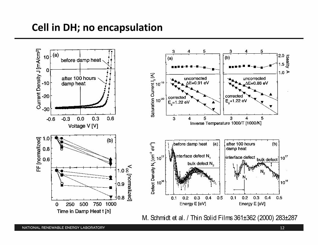
Cell in DH; no encapsulation
M. Schmidt et al. / Thin Solid Films 361±362 (2000) 283±287

13
PL of cells after damp heat exposure
DH effects:• Decrease in absorber doping(increase in defect level density)• Increase in junction recombination

14
Light soaking: early Siemens cells
D. Willett, IEEE PVSC, 1993

Process understanding/ quality improvement:
Case studies from past NREL work

16
60
50
40
30
20
10
040302010
Sputter Time (min)
Cu Ga Se In
S2212
Comparison of NREL and SSI absorbers
CIGSS
ZnO
17
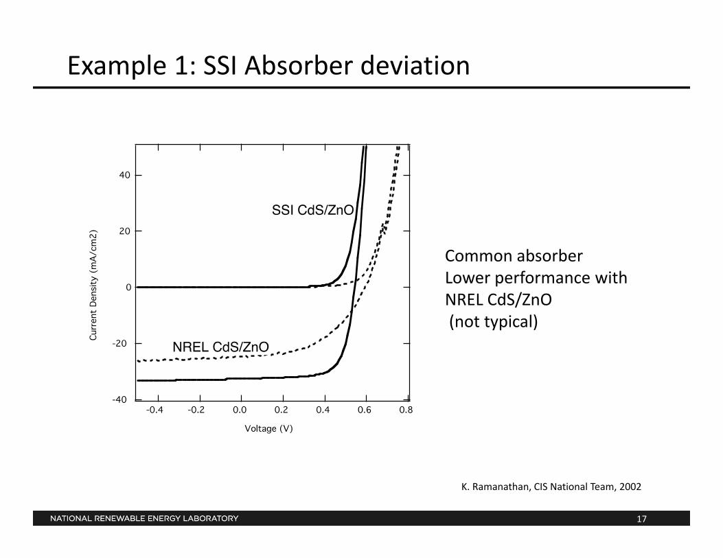
Comparison of J-V Curves
Example 1: SSI Absorber deviation
Common absorberLower performance with NREL CdS/ZnO(not typical)
K. Ramanathan, CIS National Team, 2002

18
J-V curve: NREL absorber CdS and ZnO processed in same runs as SSI
NREL absorber/ windows OK!

19
PL Spectra
SSI windows
NREL windows
Left most 2 curves: NREL CdS, no air anneal.
Green: 5’/200C/air anneal after CdS
Right most 3 curves: PL from 3 cells with SSI windows.
NREL CdS/ZnO
SSI CdS/ZnO

20
External QE Comparison
Long wave edge influenced by
•Poor Diffusion Length
•Drift assisted collection
•ZnO reflectance
•Band gap grading
•Extracting band gap not straightforward in SSI cells.
There appears to be a shift!
Same direction as PL peak shift.
Quantum efficiency

21
Compositional analysis
Revealed a large drop in the Cu ratio for the batch of absorbers.

22
Example 2: Junction anneal to improve performance
K. Ramanathan, NREL, 2002, unpublished

A Shell Renewables companyShell Solar
Thermal Degradation Characteristics
ST40 Module - Daystar Outdoor Tests
0
0.5
1
1.5
2
2.5
3
0 5 10 15 20 25
Voltage (V)
Cur
rent
(A)
Initial200h1000hEfficiency:
Initial = 11.2%200h = 9.9%1000h = 8.6%
No Loss
20% Loss
5% Loss
A Shell Renewables companyShell Solar
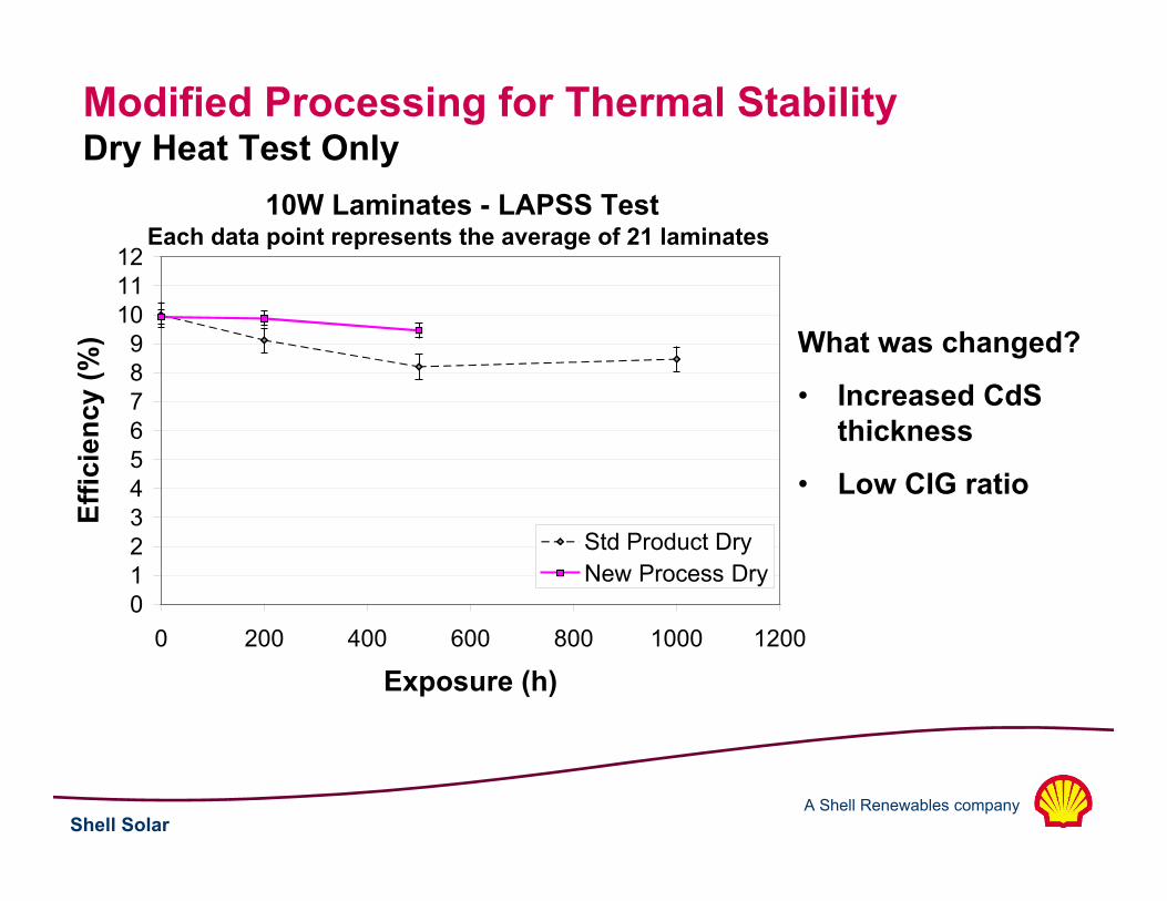
Modified Processing for Thermal StabilityDry Heat Test Only
What was changed?
• Increased CdSthickness
• Low CIG ratio
10W Laminates - LAPSS TestEach data point represents the average of 21 laminates
0123456789
101112
0 200 400 600 800 1000 1200
Exposure (h)
Effic
ienc
y (%
)
Std Product DryNew Process Dry

25
Summary
• Proper encapsulation of CIGS devices can alleviate much of the moisture driven performance degradation.
• It is possible the high efficiency devices exhibit fewer metastable effects. Efficiency improvement efforts may pay off in stability.
• A case by case approach is needed to optimize devices for performance and long term stability.

26
Note added March 5, 2012
• Important questions were raised in the afternoon discussion session that call for clarifications and further work on how CIGS devices are affected by moisture.
• Siemens/ Shell Gen II arrays have demonstrated stable operation at the OTF.• A recent NREL study of Shell’s Eclipse 80 modules showed excellent stability and
negligible effect of moisture because of improved packaging and edge seals. A paper that just appeared [Solar Energy Materials & Solar Cells 98 (2012) 398–403 ] showed that a new edge seal design enabled stable performance for 3000 h in damp heat.
• It is not possible to draw definitive conclusions about the moisture sensitivity of CIGS based on the available reports on unencapsulated cells.
Related Documents