Chipcon Chipcon Chipcon Chipcon SmartRF SmartRF SmartRF SmartRF â CC1010 This document contains information on a preproduction product. Specifications and information herein are subject to change without notice. Chipcon AS SmartRF â CC1010 PRELIMINARY Datasheet (rev. 1.0) 2002-09-18 Page 1 of 133 CC1010 Single Chip Very Low Power RF Transceiver with 8051-Compatible Microcontroller Applications • Very low power UHF wireless data transmitters and receivers • 315 / 433 / 868 and 915 MHz ISM/SRD band systems • Home automation and security • AMR – Automatic Meter Reading • RKE – Remote Keyless Entry with acknowledgement • Low power telemetry • Toys Product Description The CC1010 is a true single-chip UHF transceiver with an integrated high performance 8051 microcontroller with 32 kB of Flash program memory. The RF transceiver can be programmed for operation in the 300 – 1000 MHz range, and is designed for very low power wireless applications. The CC1010 together with a few external passive components constitutes a powerful embedded system with wireless communication capabilities. CC1010 is based on Chipcon’s SmartRF â 02 technology in 0.35 µm CMOS. Key Features • 300-1000 MHz RF Transceiver • Very low current consumption • High sensitivity (typically -107 dBm) • Programmable output power up to +10 dBm • Data rate up to 76.8 kbit/s • Very few external components • Fast PLL settling allowing frequency hopping protocols • RSSI • EN 300 220 and FCC CFR47 part 15 compliant • 8051-Compatible Microcontroller • Typically 2.5 times the performance of a standard 8051 • 32 kB Flash, 2048 + 128 Byte SRAM • 3 channel 10 bit ADC, 4 timers / 2 PWMs, 2 UARTs, RTC, Watchdog, SPI, DES encryption, 26 general I/O pins • In-circuit interactive debugging is supported for the Keil µVision2 IDE through a simple serial interface. • 2.7 - 3.6 V supply voltage • 64-lead TQFP

Welcome message from author
This document is posted to help you gain knowledge. Please leave a comment to let me know what you think about it! Share it to your friends and learn new things together.
Transcript

ChipconChipconChipconChipcon SmartRF SmartRF SmartRF SmartRF CC1010
This document contains information on a preproduction product. Specifications and information herein are subject to change without notice.
Chipcon AS SmartRF CC1010 PRELIMINARY Datasheet (rev. 1.0) 2002-09-18 Page 1 of 133
CC1010 Single Chip Very Low Power RF Transceiver with 8051-Compatible Microcontroller
Applications • Very low power UHF wireless data
transmitters and receivers • 315 / 433 / 868 and 915 MHz ISM/SRD
band systems • Home automation and security • AMR – Automatic Meter Reading
• RKE – Remote Keyless Entry with acknowledgement
• Low power telemetry • Toys
Product DescriptionThe CC1010 is a true single-chip UHF transceiver with an integrated high performance 8051 microcontroller with 32 kB of Flash program memory. The RF transceiver can be programmed for operation in the 300 – 1000 MHz range, and is designed for very low power wireless applications.
The CC1010 together with a few external passive components constitutes a powerful embedded system with wireless communication capabilities.
CC1010 is based on Chipcon’s SmartRF02 technology in 0.35 µm CMOS.
Key Features• 300-1000 MHz RF Transceiver
• Very low current consumption • High sensitivity (typically -107 dBm) • Programmable output power up to
+10 dBm • Data rate up to 76.8 kbit/s • Very few external components • Fast PLL settling allowing frequency
hopping protocols • RSSI • EN 300 220 and FCC CFR47 part
15 compliant
• 8051-Compatible Microcontroller • Typically 2.5 times the performance
of a standard 8051 • 32 kB Flash, 2048 + 128 Byte SRAM • 3 channel 10 bit ADC, 4 timers / 2
PWMs, 2 UARTs, RTC, Watchdog, SPI, DES encryption, 26 general I/O pins
• In-circuit interactive debugging is supported for the Keil µVision2 IDE through a simple serial interface.
• 2.7 - 3.6 V supply voltage • 64-lead TQFP
ChipconChipconChipconChipcon SmartRF SmartRF SmartRF SmartRF CC1010
Chipcon AS SmartRF CC1010 PRELIMINARY Datasheet (rev. 1.0) 2002-09-18 Page 2 of 133
Table Of Contents FEATURES ............................................................................................................................................ 4 ABSOLUTE MAXIMUM RATINGS .................................................................................................. 5 RECOMMENDED OPERATING CONDITIONS............................................................................. 5 DC CHARACTERISTICS.................................................................................................................... 6 ELECTRICAL SPECIFICATIONS .................................................................................................... 7 PIN CONFIGURATION..................................................................................................................... 11 PIN DESCRIPTION............................................................................................................................ 13 BLOCK DIAGRAM ............................................................................................................................ 16 8051 CORE........................................................................................................................................... 17
GENERAL DESCRIPTION ...................................................................................................................... 17 RESET ................................................................................................................................................. 17 MEMORY MAP.................................................................................................................................... 18 CPU REGISTERS ................................................................................................................................. 21 INSTRUCTION SET SUMMARY ............................................................................................................. 22 INTERRUPTS........................................................................................................................................ 26 MAIN CRYSTAL OSCILLATOR ............................................................................................................. 30 POWER AND CLOCK MODES ............................................................................................................... 31 FLASH PROGRAM MEMORY................................................................................................................ 34 SPI FLASH PROGRAMMING................................................................................................................. 34 8051 FLASH PROGRAMMING .............................................................................................................. 39 FLASH POWER CONTROL .................................................................................................................... 40 IN CIRCUIT DEBUGGING ..................................................................................................................... 41 CHIP VERSION / REVISION .................................................................................................................. 42
8051 PERIPHERALS .......................................................................................................................... 43 GENERAL PURPOSE I/O....................................................................................................................... 43 TIMER 0 / TIMER 1.............................................................................................................................. 48 TIMER 2 / 3 WITH PWM ..................................................................................................................... 54 POWER ON RESET (BROWN-OUT DETECTION) ................................................................................... 57 WATCHDOG TIMER............................................................................................................................. 58 REALTIME CLOCK............................................................................................................................... 61 SERIAL PORT 0 AND 1......................................................................................................................... 62 SPI MASTER....................................................................................................................................... 67 DES ENCRYPTION / DECRYPTION....................................................................................................... 70 RANDOM BIT GENERATION ................................................................................................................ 74 ADC................................................................................................................................................... 75
RF TRANSCEIVER ............................................................................................................................ 78 GENERAL DESCRIPTION ...................................................................................................................... 78 RF TRANSCEIVER BLOCK DIAGRAM .................................................................................................. 78 RF APPLICATION CIRCUIT .................................................................................................................. 80 TRANSCEIVER CONFIGURATION OVERVIEW ....................................................................................... 83 RF TRANSCEIVER RX/TX CONTROL AND POWER MANAGEMENT ....................................................... 84 DATA MODEM AND DATA MODES...................................................................................................... 86 BAUDRATES........................................................................................................................................ 89 TRANSMITTING AND RECEIVING DATA................................................................................................ 90 DEMODULATION AND DATA DECISION ................................................................................................ 92 SYNCHRONIZATION AND PREAMBLE DETECTION ................................................................................ 96 RECEIVER SENSITIVITY VERSUS DATA RATE AND FREQUENCY SEPARATION ....................................... 99 FREQUENCY PROGRAMMING............................................................................................................. 100 LOCK INDICATION ............................................................................................................................ 102 RECOMMENDED SETTINGS FOR ISM FREQUENCIES.......................................................................... 103 VCO................................................................................................................................................. 105

ChipconChipconChipconChipcon SmartRF SmartRF SmartRF SmartRF CC1010
Chipcon AS SmartRF CC1010 PRELIMINARY Datasheet (rev. 1.0) 2002-09-18 Page 3 of 133
VCO AND PLL SELF-CALIBRATION.................................................................................................. 105 VCO, LNA AND BUFFER CURRENT CONTROL................................................................................... 110 INPUT / OUTPUT MATCHING ............................................................................................................. 112 OUTPUT POWER PROGRAMMING ...................................................................................................... 113 RSSI OUTPUT................................................................................................................................... 115 IF OUTPUT ....................................................................................................................................... 116 OPTIONAL LC FILTER....................................................................................................................... 117 RESERVED REGISTERS AND TEST REGISTERS..................................................................................... 118 SYSTEM CONSIDERATIONS AND GUIDELINES.................................................................................... 120 PCB LAYOUT RECOMMENDATIONS.................................................................................................. 122 ANTENNA CONSIDERATIONS ............................................................................................................ 122
PACKAGE DESCRIPTION (TQFP-64) ......................................................................................... 123 SOLDERING INFORMATION....................................................................................................... 124 TRAY SPECIFICATION ................................................................................................................. 124 CARRIER TAPE AND REEL SPECIFICATION ......................................................................... 124 LIST OF ABBREVIATIONS ........................................................................................................... 125 SFR SUMMARY................................................................................................................................ 126 ALPHABETIC REGISTER INDEX................................................................................................ 130 ORDERING INFORMATION......................................................................................................... 133

ChipconChipconChipconChipcon SmartRF SmartRF SmartRF SmartRF CC1010
Chipcon AS SmartRF CC1010 PRELIMINARY Datasheet (rev. 1.0) 2002-09-18 Page 4 of 133
Features• Fully Integrated UHF RF Transceiver
• Programmable frequency in the range 300 – 1000 MHz
• High sensitivity (typically -107 dBm at 2.4 kBaud)
• Programmable output power –20 to +10 dBm
• Very low current consumption (RX: 9.1 mA)
• Very few external components required and no external RF switch or IF filter required
• Single port antenna connection • Fast PLL settling allows frequency
hopping protocols • FSK modulation with a data rate of
up to 76.8 kBaud • Manchester or NRZ coding and
decoding of data performed in hardware. Byte delineation of data can be performed in hardware to lessen the processor burden
• RSSI output which can be sampled by on-chip ADC
• Complies with EN 300 220 and FCC CFR47 part 15
• High-Performance and Low-Power 8051-Compatible Microcontroller • Optimised 8051-core which typically
gives 2.5x the performance of a standard 8051
• Dual data pointers • Idle and sleep modes • In-circuit interactive debugging is
supported for the Keil µVision IDE through a simple serial interface
• Data and Nonvolatile Program Memory • 32 kB of nonvolatile Flash memory
in-system programmable through a simple SPI interface or by the 8051 core.
• Typical Flash memory endurance: 20 000 write/erase cycles
• Programmable read and write lock of portions of Flash memory for software security
• 2048 + 128 Byte of internal SRAM • Hardware DES Encryption /
Decryption • DES supported in hardware • Output Feedback Mode or Cipher
Feedback Mode DES to avoid the requirement that data length must be a multiple of eight bytes
• Peripheral Features • Power On Reset / Brown-Out
Detection • Three channel, max 23 kSample/s,
10 bit ADC • Programmable watchdog timer. • Real time clock with 32 kHz crystal
oscillator • Two timers / pulse counters and two
timers / pulse width modulators • Two programmable serial UARTs. • Master SPI interface • 26 configurable general-purpose
I/O-pins • Random bit generator in hardware
• Low Power • 8051 core and peripherals can use
the RTC's 32 kHz clock • Idle and sleep modes for reduced
power consumption. System can wake up on interrupt or when ADC input exceeds a set threshold
• Low-power fully static CMOS design • Operating Conditions
• 2.7 - 3.6 V supply voltage • -40 - 85 °C operational temperature • 3 - 24 MHz crystal (up to 50 ppm)
for the main crystal oscillator • Packaging
• 64-lead TQFP
ChipconChipconChipconChipcon SmartRF SmartRF SmartRF SmartRF CC1010
Chipcon AS SmartRF CC1010 PRELIMINARY Datasheet (rev. 1.0) 2002-09-18 Page 5 of 133
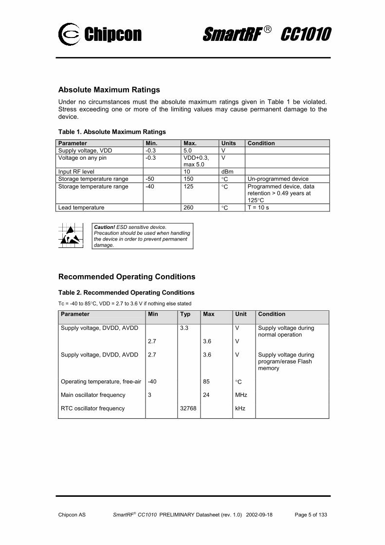
Absolute Maximum Ratings Under no circumstances must the absolute maximum ratings given in Table 1 be violated. Stress exceeding one or more of the limiting values may cause permanent damage to the device.
Table 1. Absolute Maximum Ratings Parameter Min. Max. Units Condition Supply voltage, VDD -0.3 5.0 V Voltage on any pin -0.3 VDD+0.3,
max 5.0 V
Input RF level 10 dBm Storage temperature range -50 150 °C Un-programmed device Storage temperature range -40 125 °C Programmed device, data
retention > 0.49 years at 125°C
Lead temperature 260 °C T = 10 s
Caution! ESD sensitive device. Precaution should be used when handling the device in order to prevent permanent damage.
Recommended Operating Conditions
Table 2. Recommended Operating Conditions Tc = -40 to 85°C, VDD = 2.7 to 3.6 V if nothing else stated Parameter
Min Typ Max Unit Condition
Supply voltage, DVDD, AVDD
2.7
3.3 3.6
V V
Supply voltage during normal operation
Supply voltage, DVDD, AVDD
2.7 3.6 V Supply voltage during program/erase Flash memory
Operating temperature, free-air
-40 85 °C
Main oscillator frequency
3 24
MHz
RTC oscillator frequency 32768 kHz

ChipconChipconChipconChipcon SmartRF SmartRF SmartRF SmartRF CC1010
Chipcon AS SmartRF CC1010 PRELIMINARY Datasheet (rev. 1.0) 2002-09-18 Page 6 of 133
DC CharacteristicsThe DC Characteristics of CC1010 are listed in Table 3 below.
Table 3. DC Characteristics Tc = 25°C, VDD = 3.3 V if nothing else stated Digital Inputs/Outputs
Min Typ Max Unit Condition
Logic "0" input voltage
0 0.3*VDD V
Logic "1" input voltage
0.7*VDD VDD V
Logic "0" output voltage 0
0.4 V Output current -2.0 mA, ports P0.3-P0.0, P1.7-P1.0, P2.7-P2.4, P2.2-P2.0
Logic "1" output voltage 2.5
VDD V Output current 2.0mA, ports P0.3-P0.0, P1.7-P1.0, P2.7-P2.4, P2.2-P2.0
Logic "0" output voltage 0
0.4 V Output current -8.0 mA, port P2.3
Logic "1" output voltage 2.5
VDD V Output current 8.0mA, port P2.3
Logic "0" input current
NA -1 µA Input signal equals GND
Logic "1" input current
NA 1 µA Input signal equals VDD
0
5
10
15
20
25
0 4 8 12 16 20 24
Frequency [MHz]
Supp
ly c
urre
nt [m
A]
Figure 1. Typical CPU core supply current vs. clock frequency

ChipconChipconChipconChipcon SmartRF SmartRF SmartRF SmartRF CC1010
Chipcon AS SmartRF CC1010 PRELIMINARY Datasheet (rev. 1.0) 2002-09-18 Page 7 of 133
Electrical Specifications
Table 4. Electrical Specifications Tc = 25°C, VDD = 3.3 V if nothing else stated
Parameter
Min. Typ. Max. Unit Condition
MCU, general
Power on reset (POR) voltage
2.7 2.9 3.1 V Tc = -40 to 85°C
Brown out voltage 2.7 2.9 3.1 V Tc = -40 to 85°C
RTC start-up time 160 ms
ADC, number of bits 10 bits
ADC, Differential Nonlinearity (DNL)
+/-0.2 LSB VDD is reference voltage
ADC, Integral Nonlinearity (INL)
+/-1.3 LSB VDD is reference voltage
ADC, Offset 3 LSB 7 Hz test tone
ADC, Total Harmonic Distortion (THD)
59 dB 7 Hz test tone
ADC, SINAD 54 9
dB bits
7 Hz test tone
ADC, internal reference tolerance
10 %
Supply Current
MCU, Active mode
14.8 1.3
mA mA
14.7456 MHz, main oscillator 32 kHz, RTC oscillator See page 31 for explanation of modes. See Figure 1 page 6 for supply current vs. clock frequency.
MCU, Idle mode 8.2 29.4
mA µA
14.7456 MHz, main oscillator 32 kHz, RTC oscillator
MCU, Power Down mode 0.2 10 µA
RF Transceiver, Receive mode, 433/868 MHz
9.1/ 11.9
mA
ChipconChipconChipconChipcon SmartRF SmartRF SmartRF SmartRF CC1010
Chipcon AS SmartRF CC1010 PRELIMINARY Datasheet (rev. 1.0) 2002-09-18 Page 8 of 133
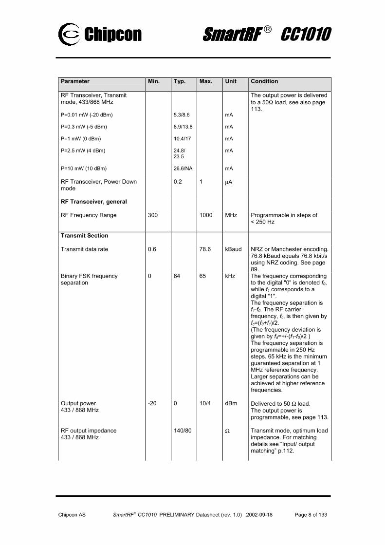
Parameter
Min. Typ. Max. Unit Condition
RF Transceiver, Transmit mode, 433/868 MHz P=0.01 mW (-20 dBm) P=0.3 mW (-5 dBm) P=1 mW (0 dBm) P=2.5 mW (4 dBm) P=10 mW (10 dBm)
5.3/8.6 8.9/13.8 10.4/17 24.8/ 23.5 26.6/NA
mA mA mA mA mA
The output power is delivered to a 50Ω load, see also page 113.
RF Transceiver, Power Down mode
0.2 1 µA
RF Transceiver, general
RF Frequency Range 300
1000 MHz Programmable in steps of < 250 Hz
Transmit Section
Transmit data rate
0.6 78.6 kBaud NRZ or Manchester encoding. 76.8 kBaud equals 76.8 kbit/s using NRZ coding. See page 89.
Binary FSK frequency separation
0 64 65 kHz The frequency corresponding to the digital "0" is denoted f0, while f1 corresponds to a digital "1". The frequency separation is f1-f0. The RF carrier frequency, fc, is then given by fc=(f0+f1)/2. (The frequency deviation is given by fd=+/-(f1-f0)/2 ) The frequency separation is programmable in 250 Hz steps. 65 kHz is the minimum guaranteed separation at 1 MHz reference frequency. Larger separations can be achieved at higher reference frequencies.
Output power 433 / 868 MHz
-20 0 10/4 dBm Delivered to 50 Ω load. The output power is programmable, see page 113.
RF output impedance 433 / 868 MHz
140/80 Ω Transmit mode, optimum load impedance. For matching details see “Input/ output matching” p.112.
ChipconChipconChipconChipcon SmartRF SmartRF SmartRF SmartRF CC1010
Chipcon AS SmartRF CC1010 PRELIMINARY Datasheet (rev. 1.0) 2002-09-18 Page 9 of 133
Parameter
Min. Typ. Max. Unit Condition
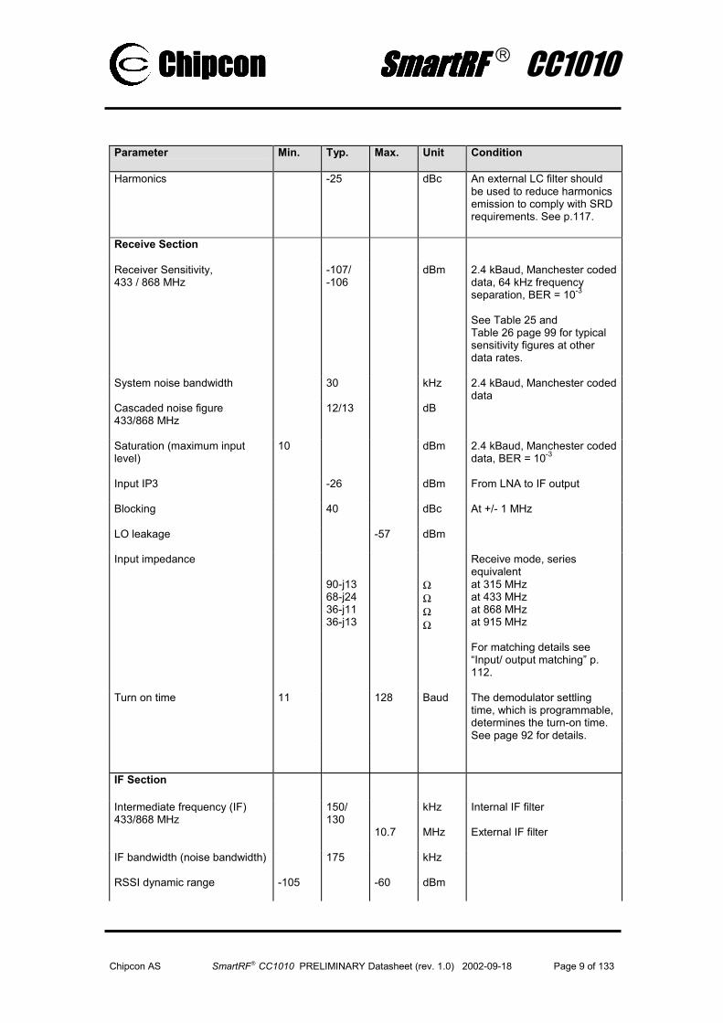
Harmonics -25 dBc An external LC filter should be used to reduce harmonics emission to comply with SRD requirements. See p.117.
Receive Section
Receiver Sensitivity, 433 / 868 MHz
-107/ -106
dBm
2.4 kBaud, Manchester coded data, 64 kHz frequency separation, BER = 10-3 See Table 25 and Table 26 page 99 for typical sensitivity figures at other data rates.
System noise bandwidth 30 kHz 2.4 kBaud, Manchester coded data
Cascaded noise figure 433/868 MHz
12/13 dB
Saturation (maximum input level)
10 dBm 2.4 kBaud, Manchester coded data, BER = 10-3
Input IP3 -26 dBm From LNA to IF output
Blocking 40 dBc At +/- 1 MHz
LO leakage -57 dBm
Input impedance
90-j13 68-j24 36-j11 36-j13
Ω Ω Ω Ω
Receive mode, series equivalent at 315 MHz at 433 MHz at 868 MHz at 915 MHz For matching details see “Input/ output matching” p. 112.
Turn on time 11 128 Baud The demodulator settling time, which is programmable, determines the turn-on time. See page 92 for details.
IF Section
Intermediate frequency (IF) 433/868 MHz
150/ 130
10.7
kHz MHz
Internal IF filter External IF filter
IF bandwidth (noise bandwidth)
175 kHz
RSSI dynamic range
-105 -60 dBm
ChipconChipconChipconChipcon SmartRF SmartRF SmartRF SmartRF CC1010
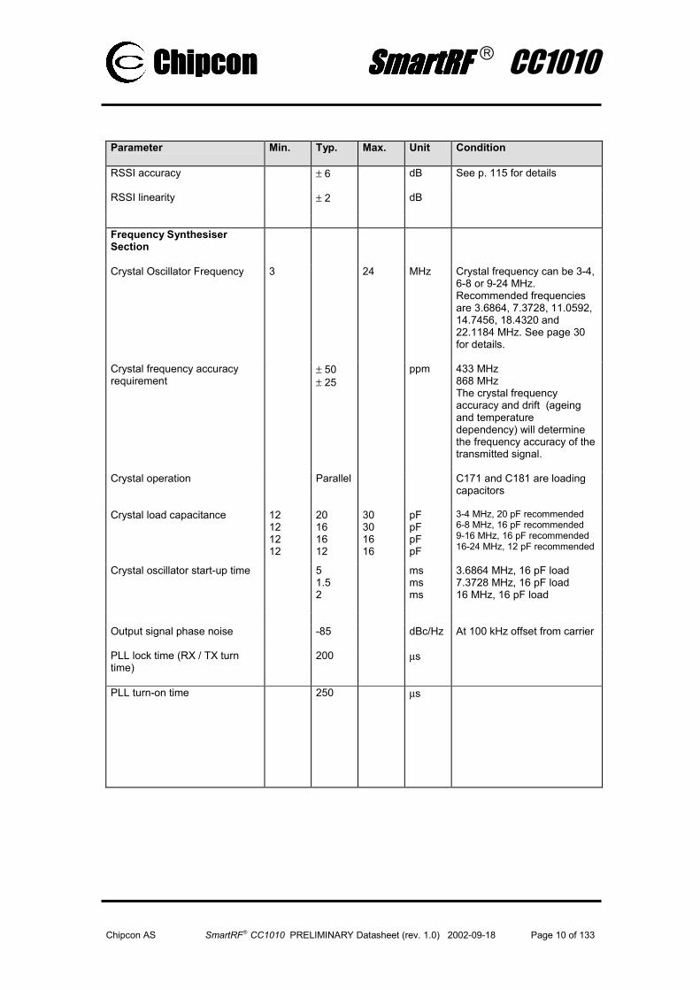
Chipcon AS SmartRF CC1010 PRELIMINARY Datasheet (rev. 1.0) 2002-09-18 Page 10 of 133
Parameter
Min. Typ. Max. Unit Condition
RSSI accuracy ± 6 dB
See p. 115 for details
RSSI linearity ± 2 dB
Frequency Synthesiser Section
Crystal Oscillator Frequency
3 24 MHz Crystal frequency can be 3-4, 6-8 or 9-24 MHz. Recommended frequencies are 3.6864, 7.3728, 11.0592, 14.7456, 18.4320 and 22.1184 MHz. See page 30 for details.
Crystal frequency accuracy requirement
± 50 ± 25
ppm 433 MHz 868 MHz The crystal frequency accuracy and drift (ageing and temperature dependency) will determine the frequency accuracy of the transmitted signal.
Crystal operation
Parallel
C171 and C181 are loading capacitors
Crystal load capacitance 12 12 12 12
20 16 16 12
30 30 16 16
pF pF pF pF
3-4 MHz, 20 pF recommended 6-8 MHz, 16 pF recommended 9-16 MHz, 16 pF recommended 16-24 MHz, 12 pF recommended
Crystal oscillator start-up time
5 1.5 2
ms ms ms
3.6864 MHz, 16 pF load 7.3728 MHz, 16 pF load 16 MHz, 16 pF load
Output signal phase noise
-85 dBc/Hz At 100 kHz offset from carrier
PLL lock time (RX / TX turn time)
200 µs
PLL turn-on time 250 µs
ChipconChipconChipconChipcon SmartRF SmartRF SmartRF SmartRF CC1010
Chipcon AS SmartRF CC1010 PRELIMINARY Datasheet (rev. 1.0) 2002-09-18 Page 11 of 133
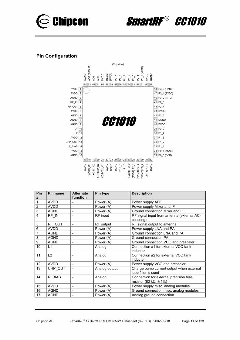
Pin Configuration
17
AGN
D
CC1010CC1010CC1010CC1010
1AVDD
2AVDD
3AGND
4RF_IN
5RF_OUT
6AVDD
7AGND
8AGND
9AGND
10L1
11L2
12AVDD
13CHP_OUT
14R_BIAS
15AVDD
16AGND
18
XOSC
_Q1
19
XOSC
_Q2
20
XOSC
32_Q
2
21
XOSC
32_Q
1
22
AGN
D
23
DG
ND
24
DG
ND
25
POR
_E
26
P1_0
27
(RXD
1) P
2_0
28
(TXD
1) P
2_1
29
(PW
M3)
P3_
5
30
(PW
M2)
P3_
4
31
(INT1
) P3_
3
32
48
47
46
45
44
43
42
41
40
39
38
37
36
35
34
33
64 63 62 61 60 59 58 57 56 55 54 53 52 51 50 49
DG
ND
P3_0 (RXD0)
P3_1 (TXD0)
P3_2 (INT0)
P2_5
P2_4
DVDD
P2_3
DGND
DVDD
P2_2
P1_4
P1_3
P1_2
P1_1
P0_1 (MOSI)
P0_0 (SCK)
AGN
D
AD2
(RSS
I/IF)
AD1
AD0
DVD
D
RES
ET
PRO
G
P2_7
P2_6
P1_7
P1_6
P1_5
P0_3
P0_2
(MIS
O)
DVD
D
DG
ND
(Top view)
Pin #
Pin name Alternate function
Pin type Description
1 AVDD - Power (A) Power supply ADC 2 AVDD - Power (A) Power supply Mixer and IF 3 AGND - Power (A) Ground connection Mixer and IF 4 RF_IN - RF input RF signal input from antenna (external AC-
coupling) 5 RF_OUT - RF output RF signal output to antenna 6 AVDD - Power (A) Power supply LNA and PA 7 AGND - Power (A) Ground connection LNA and PA 8 AGND - Power (A) Ground connection PA 9 AGND - Power (A) Ground connection VCO and prescaler 10 L1 - Analog Connection #1 for external VCO tank
inductor 11 L2 - Analog Connection #2 for external VCO tank
inductor 12 AVDD - Power (A) Power supply VCO and prescaler 13 CHP_OUT - Analog output Charge pump current output when external
loop filter is used 14 R_BIAS - Analog Connection for external precision bias
resistor (82 kΩ, ± 1%) 15 AVDD - Power (A) Power supply misc. analog modules 16 AGND - Power (A) Ground connection misc. analog modules 17 AGND - Power (A) Analog ground connection

ChipconChipconChipconChipcon SmartRF SmartRF SmartRF SmartRF CC1010
Chipcon AS SmartRF CC1010 PRELIMINARY Datasheet (rev. 1.0) 2002-09-18 Page 12 of 133
Pin #
Pin name Alternate function
Pin type Description
18 XOSC_Q1 - Analog input 3-24 MHz crystal, pin 1 or external clock input
19 XOSC_Q2 - Analog output 3-24 MHz crystal, pin 2 20 XOSC32_Q
2 - Analog output 32 kHz crystal pin2
21 XOSC32_Q1
- Analog input 32 kHz crystal pin1 or external clock input
22 AGND - Power (A) Analog ground connection 23 DGND - Power (D) Digital ground connection 24 DGND - Power (D) Digital ground connection 25 POR_E - Digital input Power-on reset enable.
0: Disable internal power-on reset module 1: Enable internal power-on reset module
26 P1.0 - Digital high-Z I/O 8051 port 1, bit 0 27 P2.0 RXD1 (I) Digital high-Z I/O 8051 port 2, bit 0 or RX of serial port 1 28 P2.1 TXD1 (O) Digital high-Z I/O 8051 port 2, bit 1 or TX of serial port 1 29 P3.5 PWM3 (O)
T1 (I) Digital high-Z I/O 8051 port 3, bit 5 or pulse width modulator
3's output or Timer / Counter 1 external input30 P3.4 PWM2 (O)
T0 (I) Digital high-Z I/O 8051 port 3, bit 4 or pulse width modulator
2's output or Timer / Counter 0 external input31 P3.3 INT1 (I) Digital high-Z I/O 8051 port 3, bit 3 or interrupt 1 input
configurable as level or edge sensitive 32 DGND - Power (D) Ground connection digital part 33 P0.0 SCK (O)
SCK (I) Digital high-Z I/O 8051 port 0, bit 0 or SPI master interface
serial clock output or Flash programming SPI slave clock input.
34 P0.1 MO (O) SI (I)
Digital high-Z I/O 8051 port 0, bit 1 or SPI interface master output or Flash programming SPI slave serial data input
35 P1.1 - Digital high-Z I/O 8051 port 1, bit 1 36 P1.2 - Digital high-Z I/O 8051 port 1, bit 2 37 P1.3 - Digital high-Z I/O 8051 port 1, bit 3 38 P1.4 - Digital high-Z I/O 8051 port 1, bit 4 39 P2.2 - Digital high-Z I/O
(Schmitt trigger input)
8051 port 2, bit 2
40 DVDD - Power (D) Digital power supply 41 DGND - Power (D) Ground connection digital part 42 P2.3 - Digital high-Z I/O (8
mA) 8051 port 2, bit 3
43 DVDD - Power (D) Digital power supply 44 P2.4 - Digital high-Z I/O 8051 port 2, bit 4 45 P2.5 - Digital high-Z I/O 8051 port 2, bit 5 46 P3.2 INT0 (I) Digital high-Z I/O 8051 port 3, bit 2 or interrupt 0 input
configurable as level or edge sensitive 47 P3.1 TXD0 (O) Digital high-Z I/O 8051 port 3, bit 1 or TX of serial port 0 48 P3.0 RXD0 (I) Digital high-Z I/O 8051 port 3, bit 0 or RX of serial port 1 49 DGND - Power (D) Digital ground connection 50 DVDD - Power (D) Digital power supply 51 P0.2 MI (I)
SO (O) Digital high-Z I/O 8051 port 0, bit 2 or SPI interface master
input or Flash programming SPI slave serial data output
52 P0.3 - Digital high-Z I/O 8051 port 0, bit 3 53 P1.5 - Digital high-Z I/O 8051 port 1, bit 5 54 P1.6 - Digital high-Z I/O 8051 port 1, bit 6

ChipconChipconChipconChipcon SmartRF SmartRF SmartRF SmartRF CC1010
Chipcon AS SmartRF CC1010 PRELIMINARY Datasheet (rev. 1.0) 2002-09-18 Page 13 of 133
Pin #
Pin name Alternate function
Pin type Description
55 P1.7 - Digital high-Z I/O 8051 port 1, bit 7 56 P2.6 - Digital high-Z I/O 8051 port 2, bit 6 57 P2.7 - Digital high-Z I/O 8051 port 2, bit 7 58 PROG - Digital input (pull-up) Flash program enable pad, active low
59 RESET - Digital input (pull-up) System reset pin, active low
60 DVDD - Power (D) Digital power supply 61 AD0 - Analog input ADC input channel 0 62 AD1 - Analog input ADC input channel 1 63 AD2 RSSI (O),
IF (O) Analog input/output ADC input channel 2, RSSI (Receiver signal
strength indicator) output, or IF output when using external demodulator
64 AGND - Power (A) Analog ground connection ADC A = Analog, D = Digital, I = input, O= Output
Pin description
AVDD, DVDD
Supply voltages for analog and digital modules respectively. All supply pins should be decoupled by capacitors. In particular, the digital and analog supply domains should be properly decoupled from each other. The placement and size of decoupling capacitors and supply filtering are critical with respect to LO leakage and sensitivity. Chipcon’s reference layout designs should be used (available from Chipcon’s website). See also page 122 for layout recommendations.
AGND, DGND
Ground for analog and digital modules respectively. Normally one common ground plane is recommended. If two separate analog and digital grounds are used they should be interconnected in one place, and one place only.
RFIN
This is the RF input, internally connected to the low noise amplifier (LNA). The signal source (antenna) should be matched to the input impedance. A DC ground is needed for LNA biasing.
RFOUT
This is the RF output, internally connected to the power amplifier (PA). The external load (antenna) should be matched to the output impedance (optimum load impedance). This pin must be DC coupled to AVDD for PA biasing (open drain output).
L1, L2
Connection to internal voltage controlled oscillator (VCO). An inductor should be connected between these pins. The inductor value will determine the VCO tuning range. The inductor should be place very close to the pins in order to minimize paracitic inductance.
CHP_OUT
Charge Pump output. If the RF transceiver is configured for external loop filter this is the current output from the charge pump. Normally the internal loop filter should be used and this pin should be left open (not connected).
RBIAS
Current output from internal band gap cell bias generator. A precision resistor (82 kΩ, ±1%) should be connected between
ChipconChipconChipconChipcon SmartRF SmartRF SmartRF SmartRF CC1010
Chipcon AS SmartRF CC1010 PRELIMINARY Datasheet (rev. 1.0) 2002-09-18 Page 14 of 133
this pin and ground to set the correct bias current level.
XOSC_Q1, XOSC_Q2
These are the main oscillator connection pins. An external crystal should be connected between these pins, and load capacitors should be connected between each pin and ground. If an external oscillator is used, the clock signal should be connected to the XOSC_Q1 pin, and XOSC_Q2 should be left open (not connected).
XOSC32_Q1, XOSC32_Q2
These are the real time clock (RTC) oscillator connection pins. An external crystal should be connected between these pins, and load capacitors should be connected between each pin and ground. If an external oscillator is used, the clock signal should be connected to the XOSC32_Q1 pin, and XOSC32_Q2 should be left open (not connected).
POR_E
Enable signal for the on-chip power-on reset module. The power-on reset is enabled when POR_E is connected to DVDD and disabled when connected to DGND.
PROG
Active low Flash programming enable pin. When this signal is active (driven to DGND) a Flash programmer can be connected to the SPI interface. Under normal operation it must be driven to DVDD.
RESET
Active low asynchronous system reset. It has an internal pull-up resistor and can be left unconnected during normal operation.
AD0, AD1
Analog inputs to A/D converter channels 0 and 1 respectively. When not used these pins can be left open (not connected).
AD2 (RSSI/IF)
Analog input to A/D converter channel 2. This pin can also be configured to be RSSI output or IF output. The pin is configured by the FREND register. When not used this pin can be left open (not connected).
PORT 0
Port 0 is a 4-bit (P0.3-P0.0) bi-directional CMOS I/O port with 2 mA drivers. A direction register (P0DIR) controls whether each pin is an output or input and the register P0 is used to read the input or control the logical value of the output.
Pins P0.0 - P0.2 can be configured to become a master SPI interface in register SPCR and will then override P0(2:0), P0DIR(2) and P0DIR(1).
Used as SPI interface, P0.0 is SCK, P0.1 is MOSI, and P0.2 is MISO.
PORT 1
Port 1 is an 8-bit (P1.7-P1.0) bi-directional CMOS I/O port with 2 mA drivers. A direction register (P1DIR) controls whether each pin is an output or input and the register P1 is used to read the input or control the logical value of the output.
PORT 2
Port 2 is an 8-bit (P2.7-P2.0) bi-directional CMOS I/O port with 2 mA drivers, except for P2.3 that has an 8 mA output buffer. A direction register (P2DIR) controls whether each pin is an output or input and the register P2 is used to read the input or control the logical value of the output.
Pins P2.0 and P2.1 can be configured to become the RXD1 and TXD1 pin, respectively, of UART 1.
PORT 3
Port 3 is a 6-bit (P3.5-P3.0) bi-directional CMOS I/O port with 2 mA drivers. A direction register (P3DIR) controls whether each pin is an output or input. The register
ChipconChipconChipconChipcon SmartRF SmartRF SmartRF SmartRF CC1010
Chipcon AS SmartRF CC1010 PRELIMINARY Datasheet (rev. 1.0) 2002-09-18 Page 15 of 133
P3 is used to read the input or control the logical value of the output.
Pins P3.0 and P3.1 can be configured to become the RXD0 and TXD0 pin, respectively, of UART 0.
Pins P3.2 and P3.3 are connected to the
external interrupt inputs INT0 and INT1 , respectively, and can cause interrupts if the corresponding interrupt enable flags
are set in register IE. The interrupts inputs can be configured to be either level-sensitive or edge-sensitive.
Pins P3.4 and P3.5 can be configured to become the pulse width modulator (PWM) outputs of Timer/PWM 2 and Timer/PWM 3, respectively. When pulse width modulation is enabled the corresponding bits in P3DIR and P3 are overridden.

ChipconChipconChipconChipcon SmartRF SmartRF SmartRF SmartRF CC1010
Chipcon AS SmartRF CC1010 PRELIMINARY Datasheet (rev. 1.0) 2002-09-18 Page 16 of 133
Block Diagram The CC1010 Block Diagram is shown in Figure 2 below.
Figure 2. CC1010 Block Diagram
32 kBFLASH
128 byteSRAM
Special FunctionRegisters(SFRs)
Inte
rrupt
Con
trolle
r
RealtimeClock
WatchdogTimer
SPI
Timers/Counters
Timers/PWMs
UARTsUARTs
Generalpurpose I/O
CODEC, Bit synchronizer,Serializer/DeserializerIF stage MODEM
RF Transceiver
8051 core
FLASHProgramming DMA
DES Module
2048 byteSRAM
RAM
Arb
iter
ResetGeneration
3-24 MHz crystal
32 kHz crystal
ClockMultiplexerSystem
clock
Port 0
Port 1
Port 2
Port 3
RESET
PROG
RF_IN
ADC
Programmable I/O (General purpose or alternate function)
Power-onreset
POR_E
Main CrystalOscillator:R
:N.n
RF_OUTLPF CHP PD
MUX
RSSIIF
BiasBias resistor
VCO inductor
VCO
CHP_OUT
AD2(RSSI/IF)
AD0AD1
PA
LNA
MIXER
L1 L2
ChipconChipconChipconChipcon SmartRF SmartRF SmartRF SmartRF CC1010
Chipcon AS SmartRF CC1010 PRELIMINARY Datasheet (rev. 1.0) 2002-09-18 Page 17 of 133
8051 Core
General description
The CC1010 microcontroller core is based on the industry-standard 8051 architecture. The MCU core is 8-bit, with program and data memory located in separate memory spaces (Harvard architecture). The internal registers are organised as four banks of 8 registers each. The instruction set supports direct, indirect and register addressing modes. Program memory can be addressed using indexed addressing. The core registers are comprised of an accumulator, a stack pointer and dual data pointer registers in addition to the general registers.
Data memory is split into internal and external RAM. The name "external RAM" is in fact misleading since in the case of the CC1010 all the RAM is internal to the chip. The difference between external and internal is that external RAM can only be accessed by a few instructions. Therefore, frequently-accessed variables as well as the stack should be kept in internal RAM.
The various peripherals are controlled through Special Function Registers (SFRs) located in the internal RAM space.
The 8051 core is instruction set compatible with the industry standard 8051. It also has one additional instruction, TRAP, to enable advanced in-circuit-debugging features. This is described on page 41.
The instruction cycle time is 4 clock cycles, which typically gives an 2.5X average reduction in instruction execution time over the original Intel 8051.
Peripheral units, including general purpose I/O, 2 standard 8051 timers, 2 extra timers with PWM functionality, a watchdog timer, a real-time clock, an SPI master interface, hardware DES encryption, a true random bit generator and ADC are all described from page 43 and out. Dual data pointers are available for faster data transfer.
Reset
CC1010 must be reset at start-up. There are several sources for reset in CC1010 :
• External reset pin, RESET . Applying a low signal to this pin at any time will reset almost all registers in CC1010. Exceptions can be found in Table 33 on page 126 The input is asynchronous and is synchronised internally, so that the reset can be released independent of the timing of the active clock signal. If the main crystal oscillator is inactive, the reset input should be held long enough for the oscillator to start up and stabilize. See Electrical Specifications page 7 for oscillator start-up timing.
• Power On Reset (POR). The internal POR module can generate reset upon power-up. Special requirements for power consumption or power supply
voltage may require an external POR module, as described in the Power On Reset (Brown-Out Detection) section at page 57.
• Brown-out detection reset. The POR will also detect low supply voltage and generate a reset.
• Watchdog timer reset. The watchdog timer can generate a reset, as described in the section on page 56.
• ADC reset. The ADC module can be programmed to generate a reset signal if its inputs exceed a programmed threshold. See the ADC section on page 75 for details.
The POR and ADC reset signals will be held for 1024 clock periods after the signal is released. This will ensure a safe clock start-up if the crystal oscillator is currently not running.
ChipconChipconChipconChipcon SmartRF SmartRF SmartRF SmartRF CC1010
Chipcon AS SmartRF CC1010 PRELIMINARY Datasheet (rev. 1.0) 2002-09-18 Page 18 of 133
Memory Map
The CC1010 memory map is shown in Figure 3.
CC1010 has 2 blocks of RAM on chip. This includes the 128 bytes Internal RAM and the 2048 bytes External RAM. (The 2048-byte RAM will be referred to as External RAM, although it is on-chip. Direct access to off-chip RAM is not implemented.)
Access to the internal RAM is performed using the MOV instruction. MOV A, @Ri, MOV @Ri, A and MOV @Ri, #data use indirect addressing. MOV A, direct, MOV Rn, direct, MOV direct, A, MOV direct, Rn, MOV direct,direct and MOV direct, #data use direct addressing. MOV @Ri, direct uses indirect and direct addressing.
All direct addressing instructions can also be used to access the SFRs. CC1010 also implements the option to access SFRs indirectly, as described in the In Circuit Debugging section on page 41. CC1010 has dual data pointers to external RAM, provided in the 16 bit registers DPTR0 and DPTR1 (SFRs DPH0, DPL0, DPH1 and DPL1). If a high-level language compilator is used, it should be set up to make use of both pointers for better performance. The data pointer is selected through DPS.SEL.
Access to the external RAM is performed using the MOVX instruction and indirect addressing using either the 16 bit data pointers or the 8 bit registers R0 or R1
together with MPAGE. MOVX A, @DPTR and MOVX @DPTR, A moves data to (from) the accumulator, from (to) the address pointed to by the currently selected data pointer.
The instructions MOVX A, @Ri and MOVX @Ri, A moves data to (from) the accumulator, from (to) the address given by the memory page address register MPAGE and the register Ri (R0 or R1). MPAGE gives the 8 most significant address bits, while the register Ri gives the 8 least significant bits. In many 8051 implementations, this type of external RAM access is performed using P2 to give the most significant address bits. Existing software may therefore have to be adapted to make use of MPAGE instead of P2.
The program memory can be read using the MOVC A, @A+DPTR and MOVC A,@A+PC instructions, which moves a byte from the program memory address given by A+DPTR or A+PC respectively. The program memory can not be written using MOV commands, but uses the method described in the 8051 Flash Programming section on page 39.
CC1010 also provides a possibility to stretch the access cycle to external RAM, through CKCON.MD(2:0) (see page 51). The default value for CKCON.MD is "001". It is recommended to set CKCON.MD to "000" for faster RAM access.

ChipconChipconChipconChipcon SmartRF SmartRF SmartRF SmartRF CC1010
Chipcon AS SmartRF CC1010 PRELIMINARY Datasheet (rev. 1.0) 2002-09-18 Page 19 of 133
Internal RAMAccessible
through Directand IndirectAddressing
0x00
0x7F
Special FunctionRegisters (SFR),
accessiblethrough Direct
Addressing
0xFF
Accesiblethrough indirect
addressing
0x7FF
Internal RAM / SFR
External RAM
0x00
Flash ProgramMemory
0x00
Accesiblethrough indirect
addressing
0x7FFF
Figure 3. Memory Map
DPL0 (0x82) - Data Pointer 0, low byte Bit Name R/W Description 7:0 DPL0(7:0) R/W Data Pointer 0, low byte
DPH0 (0x83) - Data Pointer 0, high byte Bit Name R/W Description 0 DPH0(7:0) R/W Data Pointer 0, high byte
DPL1 (0x84) - Data Pointer 1, low byte Bit Name R/W Description 7:0 DPL1(7:0) R/W Data Pointer 1, low byte
DPH1 (0x85) - Data Pointer 1, high byte Bit Name R/W Description 7:0 DPH1(7:0) R/W Data Pointer 1, high byte

ChipconChipconChipconChipcon SmartRF SmartRF SmartRF SmartRF CC1010
Chipcon AS SmartRF CC1010 PRELIMINARY Datasheet (rev. 1.0) 2002-09-18 Page 20 of 133
DPS (0x86) - Data Pointer Select Bit Name R/W Description 7:1 - R0 Reserved, read as 0 0 SEL R/W Data Pointer Select for external RAM access
0 : DPH0 and DPL0 are used 1 : DPH1 and DPL1 are used
MPAGE (0x92) - Memory Page Select Register Bit Name R/W Description 7:0 MPAGE(7:0) R/W Memory Page
A total of 119 Special Function Registers (SFRs) are accessible from the microcontroller core. The names and addresses of all SFRs are listed in Table 5. All standard 8051 registers are available, in addition to SFRs which are CC1010 specific, controlling modules such as the RF Transceiver, DES encryption, ADC and Real-Time Clock.
All SFRs will be described in the following sections. A more detailed overview is provided in Table 33 on page 126, which also includes all reset values. SFRs with addresses ending with 0 or 8 (leftmost column of Table 5) are bit adressable.
Table 5. CC1010CC1010CC1010CC1010 SFR Overview 0/8 1/9 2/A 3/B 4/C 5/D 6/E 7/F 0xF8 EIP TEST0 TEST1 TEST2 TEST3 TEST4 TEST5 TEST6
0xF0 B FSHAPE7 FSHAPE6 FSHAPE5 FSHAPE4 FSHAPE3 FSHAPE2 FSHAPE1
0xE8 EIE FSDELAY FSEP0 FSEP1 FSCTRL RTCON FREND TESTMUX
0xE0 ACC CURRENT PA_POW PLL LOCK CAL PRESCALER RESERVED
0xD8 EICON MODEM2 MODEM1 MODEM0 MATCH FLTIM - -
0xD0 PSW X32CON WDT PDET BSYNC - - -
0xC8 RFMAIN RFBUF FREQ_0A FREQ_1A FREQ_2A FREQ_0B FREQ_1B FREQ_2B
0xC0 SCON1 SBUF1 RFCON CRPCON CRPKEY CRPDAT CRPCNT RANCON
0xB8 IP RDATA RADRL RADRH CRPINI4 CRPINI5 CRPINI6 CRPINI7
0xB0 P3 - - - CRPINI0 CRPINI1 CRPINI2 CRPINI3
0xA8 IE TCON2 T2PRE T3PRE T2 T3 FLADR FLCON
0xA0 P2 SPCR SPDR SPSR P0DIR P1DIR P2DIR P3DIR
0x98 SCON0 SBUF0 - - - - - CHVER
0x90 P1 EXIF MPAGE ADCON ADDATL ADDATH ADCON2 ADTRH
0x88 TCON TMOD TL0 TL1 TH0 TH1 CKCON -
0x80 P0 SP DPL0 DPH0 DPL1 DPH1 DPS PCON
ChipconChipconChipconChipcon SmartRF SmartRF SmartRF SmartRF CC1010
Chipcon AS SmartRF CC1010 PRELIMINARY Datasheet (rev. 1.0) 2002-09-18 Page 21 of 133
CPU Registers
CC1010 provides 4 register banks of 8 registers each. These register banks are mapped in the the internal data memory (see the Memory section on page 31) at addresses 0x00 - 0x07, 0x08 - 0x0F, 0x10 - 0x17 and 0x18 - 0x1F. Each register bank contains the 8 8-bit registers R0 through R7. The different register banks are selected through the Program Status Word PSW.RS(1:0) as shown below. PSW also contains carry, overflow and
parity flags that reflect the current CPU state.
In addition, the CPU uses the accumulator register A (accessed via the SFR space as ACC), B (for multiplication and division) and the stack pointer SP. These registers are shown below. Note that the hardware stack pointer SP is increased when pushing and decreased when popping data, unlike many other microcontroller architectures.
PSW (0xD0) - Program Status Word Bit Name R/W Description 7 CY R/W Carry Flag, set to 1 when the last arithmetic operation resulted in a
carry (during addition) or borrow (during subtraction), otherwise cleared to 0 by all arithmetic operations. CY is also used for rotation instructions.
6 AC R/W Auxiliary carry flag. Set to 1 when the last arithmetic operation resulted in a carry into (during addition) or borrow from (during subtraction) the high order nibble, otherwise cleared to 0 by all arithmetic operations.
5 F0 R/W Flag 0 (Available to the user for general purpose) 4 RS1 R/W 3 RS0 R/W
Register bank select. RS1 RS0 Working register bank and address 0 0 Bank0 0x00-0x07 0 1 Bank1 0x08-0x0F 1 0 Bank2 0x10-0x17 1 1 Bank3 0x18-0x1F
2 OV R/W Overflow flag. Set to 1 when the last arithmetic operation resulted in a carry (addition), borrow (subtraction), or overflow (multiply or divide). Otherwise, the bit cleared to 0 by all arithmetic operations.
1 F1 R/W Flag 1 (Available to the user for general purpose) 0 P R/W Parity flag. Set to 1 when the modulo-2 sum of the 8 bits in the
accumulator is 1 (odd parity), cleared to 0 on even parity.
ACC (0xE0) - Accumulator Register Bit Name R/W Description 7:0 ACC(7:0) R/W Accumulator
B (0xF0) - B Register Bit Name R/W Description 7:0 B(7:0) R/W B is used for multiplication and division
SP (0x81) - Stack Pointer Bit Name R/W Description 7:0 SP(7:0) R/W Stack Pointer, used for pushing and poping data to and from the
stack. Note that the reset value for SP is 0x07

ChipconChipconChipconChipcon SmartRF SmartRF SmartRF SmartRF CC1010
Chipcon AS SmartRF CC1010 PRELIMINARY Datasheet (rev. 1.0) 2002-09-18 Page 22 of 133
Instruction Set SummaryThe 8051 instruction set is summarised in Table 6 below. All mnemonics are copyright Intel Corporation 1980.
One non-standard 8051 instruction, TRAP, with opcode 0xA5 is included to enable setting of breakpoints. This instruction is described in the In Circuit Debugging section at page 41. Symbols used in the table are:
• A - Accumulator
• AB - Register pair A and B
• B - Multiplication register
• C - Carry flag
• DPTR - Data pointer
• Rn - Register R0 - R7
• PC - Program counter
• direct - 8-bit data address (Internal RAM 0x00 - 0x7F, SFRs 0x80-0xFF)
• @Ri - Internal register pointed to by R0 or R1 (except MOVX)
• rel - Two's complement offset byte used by SJMP and conditional jumps
• bit - Direct bit address
• #data - 8-bit constant
• #data 16 - 16-bit constant
• addr 16 - 16-bit destination address
• addr 11 - 11-bit destination address, used by ACALL and AJMP. The branch will be within the same 2 kB block of program memory of the first byte of the following instruction.
The ‘Bytes’ column shows the number of bytes of Flash memory used. Further, the number of instruction cycles is shown. Each instruction cycle require four clock cycles. The 4 rightmost columns shows which flags in the program status word PSW (see page 21) are affected by the instructions.
Table 6. Instruction Set Summary Mnemonic Description
Byt
es
Inst
r. C
ycle
s
Hex
Opc
ode
CY
AC
OV
P
ADD A, Rn Add register to A 1 1 28-2F x x x x ADD A, direct Add direct byte to A 2 2 25 x x x x ADD A, @Ri Add data memory to A 1 1 26-27 x x x x ADD A, #data Add immediate to A 2 2 24 x x x x ADDC A, Rn Add register to A with carry 1 1 38-3F x x x x ADDC A, direct Add direct byte to A with carry 2 2 35 x x x x ADDC A, @Ri Add data memory to A with carry 1 1 36-37 x x x x ADDC A, #data Add immediate to A with carry 2 2 34 x x x x SUBB A, Rn Subtract register from A with
borrow 1 1 98-9F x x x x
SUBB A, direct Subtract direct byte from A with borrow
2 2 95 x x x x
SUBB A, @Ri Subtract data memory from A with borrow
1 1 96-97 x x x x
SUBB A, #data Subtract immediate from A with borrow
2 2 94 x x x x

ChipconChipconChipconChipcon SmartRF SmartRF SmartRF SmartRF CC1010
Chipcon AS SmartRF CC1010 PRELIMINARY Datasheet (rev. 1.0) 2002-09-18 Page 23 of 133
Mnemonic Description
Byt
es
Inst
r. C
ycle
s
Hex
Opc
ode
CY
AC
OV
P
INC A Increment A 1 1 04 x INC Rn Increment register 1 1 08-0F INC direct Increment direct byte 2 2 05 INC @Ri Increment data memory 1 1 06-07 DEC A Decrement A 1 1 14 x DEC Rn Decrement register 1 1 18-1F DEC direct Decrement direct byte 2 2 15 DEC @Ri Decrement data memory 1 1 16-17 INC DPTR Increment data pointer 1 3 A3 MUL AB Multiply A by B 1 5 A4 x x x DIV AB Divide A by B 1 5 84 x x x DA A Decimal adjust A 1 1 D4 x x
Logical ANL A, Rn AND register to A 1 1 58-5F x ANL A, direct AND direct byte to A 2 2 55 x ANL A, @Ri AND data memory to A 1 1 56-57 x ANL A, #data AND immediate to A 2 2 54 x ANL direct, A AND A to direct byte 2 2 52 ANL direct, #data AND immediate data to direct byte 3 3 53 ORL A, Rn OR register to A 1 1 48-4F x ORL A, direct OR direct byte to A 2 2 45 x ORL A, @Ri OR data memory to A 1 1 46-47 x ORL A, #data OR immediate to A 2 2 44 x ORL direct, A OR A to direct byte 2 2 42 ORL direct, #data OR immediate data to direct byte 3 3 43 XRL A, Rn Exclusive-OR register to A 1 1 68-6F x XRL A, direct Exclusive-OR direct byte to A 2 2 65 x XRL A, @Ri Exclusive-OR data memory to A 1 1 66-67 x XRL A, #data Exclusive-OR immediate to A 2 2 64 x XRL direct, A Exclusive-OR A to direct byte 2 2 62 XRL direct, #data Exclusive-OR immediate to direct
byte 3 3 63
CLR A Clear A 1 1 E4 x CPL A Complement A 1 1 F4 x SWAP A Swap nibbles of A 1 1 C4 RL A Rotate A left 1 1 23 RLC A Rotate A left through carry 1 1 33 x x RR A Rotate A right 1 1 03 RRC A Rotate A right through carry 1 1 13 x x
Data Transfer MOV A, Rn Move register to A 1 1 E8-
EF x
MOV A, direct Move direct byte to A 2 2 E5 x MOV A, @Ri Move data memory to A 1 1 E6-
E7 x
MOV A, #data Move immediate to A 2 2 74 x MOV Rn, A Move A to register 1 1 F8-FF

ChipconChipconChipconChipcon SmartRF SmartRF SmartRF SmartRF CC1010
Chipcon AS SmartRF CC1010 PRELIMINARY Datasheet (rev. 1.0) 2002-09-18 Page 24 of 133
Mnemonic Description
Byt
es
Inst
r. C
ycle
s
Hex
Opc
ode
CY
AC
OV
P
MOV Rn, direct Move direct byte to register 2 2 A8-AF
MOV Rn, #data Move immediate to register 2 2 78-7F MOV direct, A Move A to direct byte 2 2 F5 MOV direct, Rn Move register to direct byte 2 2 88-8F MOV direct,direct
Move direct byte to direct byte 3 3 85
MOV direct, @Ri Move data memory to direct byte 2 2 86-87 MOV direct, #data Move immediate to direct byte 3 3 75 MOV @Ri, A MOV A to data memory 1 1 F6-F7 MOV @Ri, direct Move direct byte to data memory 2 2 A6-
A7
MOV @Ri, #data Move immediate to data memory 2 2 76-77 MOV DPTR, #data Move immediate to data pointer 3 3 90 MOVC A, @A+DPTR Move code byte relative DPTR to
A 1 3 93 x
MOVC A, @A+PC Move code byte relative PC to A 1 3 83 x MOVX A, @Ri Move external data (A8) to A 1 2-9 E2-
E3 x
MOVX A, @DPTR Move external data (A16) to A 1 2-9 E0 x MOVX @Ri, A Move A to external data (A8) 1 2-9 F2-F3 MOVX @DPTR, A Move A to external data (A16) 1 2-9 F0 PUSH direct Push direct byte onto stack 2 2 C0 POP direct Pop direct byte from stack 2 2 D0 XCH A, Rn Exchange A and register 1 1 C8-
CF x
XCH A, direct Exchange A and direct byte 2 2 C5 x XCH A, @Ri Exchange A and data memory 1 1 C6-
C7 x
XCHD A, @Ri Exchange A and data memory nibble
1 1 D6-D7
x
Boolean CLR C Clear carry 1 1 C3 x CLR bit Clear direct bit 2 2 C2 SETB C Set carry 1 1 D3 x SETB bit Set direct bit 2 2 D2 CPL C Complement carry 1 1 B3 x CPL bit Complement direct bit 2 2 B2 ANL C, bit AND direct bit to carry 2 2 82 x ANL C, /bit AND direct bit inverse to carry 2 2 B0 x ORL C, bit OR direct bit to carry 2 2 72 x ORL C, /bit OR direct bit inverse to carry 2 2 A0 x MOV C, bit Move direct bit to carry 2 2 A2 x MOV bit, C Move carry to direct bit 2 2 92
Branching ACALL addr 11 Absolute call to subroutine 2 3 11-F1 LCALL addr 16 Long call to subroutine 3 4 12 RET Return from subroutine 1 4 22

ChipconChipconChipconChipcon SmartRF SmartRF SmartRF SmartRF CC1010
Chipcon AS SmartRF CC1010 PRELIMINARY Datasheet (rev. 1.0) 2002-09-18 Page 25 of 133
Mnemonic Description
Byt
es
Inst
r. C
ycle
s
Hex
Opc
ode
CY
AC
OV
P
RETI Return from interrupt 1 4 32 AJMP addr 11 Absolute jump unconditional 2 3 01-E1 LJMP addr 16 Long jump unconditional 3 4 02 SJMP rel Short jump (relative address) 2 3 80 JC rel Jump on carry = 1 2 3 40 JNC rel Jump on carry = 0 2 3 50 JB bit, rel Jump on direct bit = 1 3 4 20 JNB bit, rel Jump on direct bit = 0 3 4 30 JBC bit, rel Jump on direct bit = 1 and clear 3 4 10 JMP @A+DPTR Jump indirect relative DPTR 1 3 73 JZ rel Jump on accumulator = 0 2 3 60 JNZ rel Jump on accumulator /= 0 2 3 70 CJNE A, direct,rel
Compare A and direct, jump relative if not equal
3 4 B5 x
CJNE A, #d, rel Compare A and immediate, jump relative if not equal
3 4 B4 x
CJNE Rn, #d, rel Compare reg and immediate, jump relative if not equal
3 4 B8-BF
x
CJNE @Ri, #d, rel Compare ind and immediate, jump relative if not equal
3 4 B6-B7
x
DJNZ Rn, rel Decrement register, jump relative if not zero
2 3 D8-DF
DJNZ direct, rel Decrement direct byte, jump relative if not zero
3 4 D5
Misc NOP No operation 1 1 00 TRAP Set EICON.FDIF = 1, used for
breakpoints 1 3 A5

ChipconChipconChipconChipcon SmartRF SmartRF SmartRF SmartRF CC1010
Chipcon AS SmartRF CC1010 PRELIMINARY Datasheet (rev. 1.0) 2002-09-18 Page 26 of 133
Interrupts
In CC1010 there are a total of 15 interrupt sources, which share 12 interrupt lines. These are all shown in Table 7. Each interrupt’s natural priority, interrupt vector,
interrupt enable and interrupt flag, which is also shown in the table, will be described below.
Table 7. CC1010CC1010CC1010CC1010 Interrupt overview Interrupt Natural
Priority Priority Control
Interrupt Vector
Interrupt Enable
Interrupt Flag
Flash / Debug interrupt 0 - 0x33 EICON.FDIE
EICON.FDIF
External Interrupt 0 1 IP.PX0 0x03 IE.EX0 TCON.IE0 (*)
Timer 0 Interrupt 2 IP.PT0 0x0B IE.ET0 TCON.TF0 (*)
External Interrupt 1 3 IP.PX1 0x13 IE.EX1 TCON.IE1 (*)
Timer 1 Interrupt 4 IP.PT1 0x1B IE.ET1 TCON.TF1 (*)
Serial Port 0 Transmit Interrupt SCON0.TI_0Serial Port 0 Receive Interrupt
5 IP.PS0 0x23 IE.ES0SCON0.RI_0
Serial Port 1 Transmit Interrupt SCON1.TI_1Serial Port 1 Receive Interrupt
6 IP.PS1 0x3B IE.ES1SCON1.TI_1
RF Transmit / Receive Interrupt 7 EIP.PRF 0x43 EIE.RFIE EXIF.RFIFTimer 2 Interrupt 8 EIP.PT2 0x4B EIE.ET2 EXIF.TF2ADC Interrupt EIE.ADIE
and ADCON2.ADCIE
EXIF.ADIF and ADCON2.ADCIF
DES Encryption / Decryption Interrupt
9 EIP.PAD 0x53
EIE.ADIEand CRPCON.CRPIE
EXIF.ADIFand CRPCON.CRPIF
Timer 3 Interrupt 10 EIP.PT3 0x5B EIE.ET3 EXIF.TF3Realtime Clock Interrupt 11 EIP.PRTC 0x63 EIE.RTCIE EICON.RTCIF(*) - Interrupt flag is cleared by hardware.
Interrupt Masking
IE.EA is the global interrupt enable for all interrupts, except the Flash / Debug interrupt. When IE.EA is set, each interrupt is masked by the interrupt enable bits listed in Table 7. When IE.EA is cleared, all interrupts are masked, except the Flash / Debug interrupt, which has its own interrupt mask bit, EICON.FDIE.
Interrupt Processing
When an enabled interrupt occurs, the CPU jumps to the address of the interrupt service routine (ISR) associated with that interrupt, as shown in Table 7. Most interrupts can also be initiated by setting the associated interrupt flag from software.
CC1010 executes the ISR to completion unless another interrupt set at an higher interrupt level occurs. Each ISR ends with a RETI (return from interrupt) instruction. After executing the RETI, CC1010 returns to the next instruction that would have been executed if the interrupt had not occurred.
CC1010 always completes the instruction in progress before servicing an interrupt. If the instruction in progress is RETI, or a write access to any of the IP, IE, EIP, or EIE SFRs, CC1010 completes one additional instruction before servicing the interrupt.

ChipconChipconChipconChipcon SmartRF SmartRF SmartRF SmartRF CC1010
Chipcon AS SmartRF CC1010 PRELIMINARY Datasheet (rev. 1.0) 2002-09-18 Page 27 of 133
IE (0xA8) - Interrupt Enable Register Bit Name R/W Description 7 EA R/W Global Interrupt enable / disable
0 : All interrupts except the Flash / debug interrupt are disabled 1 : Each interrupt is enabled by its individual masking bit
6 ES1 R/W Serial Port 1 interrupt enable / disable 0 : Interrupt is disabled 1 : Interrupt is enabled, when also EA is set
5 - R/W Reserved for future use 4 ES0 R/W Serial Port 0 interrupt enable / disable
0 : Interrupt is disabled 1 : Interrupt is enabled, when also EA is set
3 ET1 R/W Timer 1 interrupt enable / disable 0 : Interrupt is disabled 1 : Interrupt is enabled, when also EA is set
2 EX1 R/W External interrupt 1 (from P3.3) enable / disable 0 : Interrupt is disabled 1 : Interrupt is enabled, when also EA is set
1 ET0 R/W Timer 0 interrupt enable / disable 0 : Interrupt is disabled 1 : Interrupt is enabled, when also EA is set
0 EX0 R/W External interrupt 0 (from P3.2) enable / disable 0 : Interrupt is disabled 1 : Interrupt is enabled, when also EA is set
EIE (0xE8) - Extended Interrupt Enable Register Bit Name R/W Description 7 - R1 Reserved, read as 1 6 - R1 Reserved, read as 1 5 - R1 Reserved, read as 1 4 RTCIE R/W Realtime Clock interrupt enable / disable
0 : Interrupt is disabled 1 : Interrupt is enabled, when also EA is set
3 ET3 R/W Timer 3 interrupt enable / disable 0 : Interrupt is disabled 1 : Interrupt is enabled, when also EA is set
2 ADIE R/W ADC / DES interrupt enable / disable 0 : Interrupt is disabled 1 : Interrupt is enabled, when also EA is set
1 ET2 R/W Timer 2 interrupt enable / disable 0 : Interrupt is disabled 1 : Interrupt is enabled, when also EA is set
0 RFIE R/W RF Interrupt enable / disable 0 : Interrupt is disabled 1 : Interrupt is enabled, when also EA is set
ChipconChipconChipconChipcon SmartRF SmartRF SmartRF SmartRF CC1010
Chipcon AS SmartRF CC1010 PRELIMINARY Datasheet (rev. 1.0) 2002-09-18 Page 28 of 133
EICON (0xD8) - Extended Interrupt Control Bit Name R/W Description 7 SMOD1 R/W Serial Port 1 baud rate doubler enable / disable
0 : Serial Port 1 baud rate is normal 1 : Serial Port 1 baud rate is doubled
6 - R1 Reserved, read as 1 5 FDIE R/W Flash / Debug interrupt enable
0 : Interrupt is disabled 1 : Interrupt is enabled (independent of IE.EA)
4 FDIF R/W Flash / Debug interrupt flag FDIF is set by hardware when an 8051-initiated write to Flash program memory is completed or a TRAP instruction is executed. FDIF may also be set by software. FDIF must be cleared by software before exiting the ISR.
3 RTCIF R/W Realtime clock interrupt flag RTCIF is set by hardware when an interrupt request is generated from the realtime clock. RTCIF may also be set by software. RTCIF must be cleared by software before exiting the ISR.
2 - R0 Reserved, read as 0 1 - R0 Reserved, read as 0 0 - R0 Reserved, read as 0
EXIF (0x91) - Extended Interrupt Flag Bit Name R/W Description 7 TF3 R/W Timer 3 interrupt flag.
TF3 is set by hardware when an interrupt request is generated from Timer 3. TF3 may also be set by software. TF3 must be cleared by software before exiting the ISR.
6 ADIF R/W ADC / DES Interrupt flag. ADIF is set by hardware when an interrupt request is generated from the ADC block (ADCON2.ADCIF) or by the DES Encryption / Decryption block (CRPCON.CRPIF). These interrupts must also be enabled by setting ADCON2.ADCIE and CRPCON.CRPIE. ADIF may also be set by software. ADIF must be cleared by software before exiting the ISR
5 TF2 R/W Timer 2 interrupt flag. TF2 is set by hardware when an interrupt request is generated from Timer 2. TF2 may also be set by software. TF2 must be cleared by software before exiting the ISR
4 RFIF R/W RF Transmit / receive interrupt flag. RFIF is set by hardware when an interrupt request is generated from the RF transceiver block. RFIF may also be set by software. RFIF must be cleared by software before exiting the ISR.
3 - R1 Reserved, read as 1 2 - R0 Reserved, read as 0 1 - R0 Reserved, read as 0 0 - R0 Reserved, read as 0
Interrupt Priority
Interrupts are prioritised in two stages: Interrupt level and natural priority. The
interrupt level (low, high or highest) takes precedence over the natural priority.
The Flash / Debug Interrupt, if enabled, always has the highest priority and is the

ChipconChipconChipconChipcon SmartRF SmartRF SmartRF SmartRF CC1010
Chipcon AS SmartRF CC1010 PRELIMINARY Datasheet (rev. 1.0) 2002-09-18 Page 29 of 133
only interrupt that can have the highest priority. All other interrupts can be assigned either low or high priority, set by the registers IP and EIP listed below.
Two interrupts with the same interrupt priority that occur simultaneously are resolved through their natural priority. The
natural priority is shown in Table 7. The interrupt having the lowest natural priority will be serviced first.
Once an interrupt is being serviced, only an interrupt of higher priority level can interrupt the service routine of the interrupt currently being serviced.
IP (0xB8) - Interrupt Priority Register Bit Name R/W Description 7 - R1 Reserved, read as 1 6 PS1 R/W Serial Port 1 interrupt priority control
0 : Interrupt has low priority 1 : Interrupt has high priority
5 - R/W Reserved for future use 4 PS0 R/W Serial Port 0 interrupt priority control
0 : Interrupt has low priority 1 : Interrupt has high priority
3 PT1 R/W Timer 1 interrupt priority control 0 : Interrupt has low priority 1 : Interrupt has high priority
2 PX1 R/W External Interrupt 1 (from P3.3) interrupt priority control 0 : Interrupt has low priority 1 : Interrupt has high priority
1 PT0 R/W Timer 0 interrupt priority control 0 : Interrupt has low priority 1 : Interrupt has high priority
0 PX0 R/W External Interrupt 0 (from P3.2) interrupt priority control 0 : Interrupt has low priority 1 : Interrupt has high priority
EIP (0xF8) - Extended Interrupt Priority Register Bit Name R/W Description 7 - R1 Reserved, read as 1 6 - R1 Reserved, read as 1 5 - R1 Reserved, read as 1 4 PRTC R/W Realtime Clock interrupt priority control
0 : Interrupt has low priority 1 : Interrupt has high priority
3 PT3 R/W Timer 3 interrupt priority control 0 : Interrupt has low priority 1 : Interrupt has high priority
2 PAD R/W ADC / DES interrupt priority control 0 : Interrupt has low priority 1 : Interrupt has high priority
1 PT2 R/W Timer 2 interrupt priority control 0 : Interrupt has low priority 1 : Interrupt has high priority
0 PRF R/W 0 : Interrupt has low priority 1 : Interrupt has high priority
ChipconChipconChipconChipcon SmartRF SmartRF SmartRF SmartRF CC1010
Chipcon AS SmartRF CC1010 PRELIMINARY Datasheet (rev. 1.0) 2002-09-18 Page 30 of 133
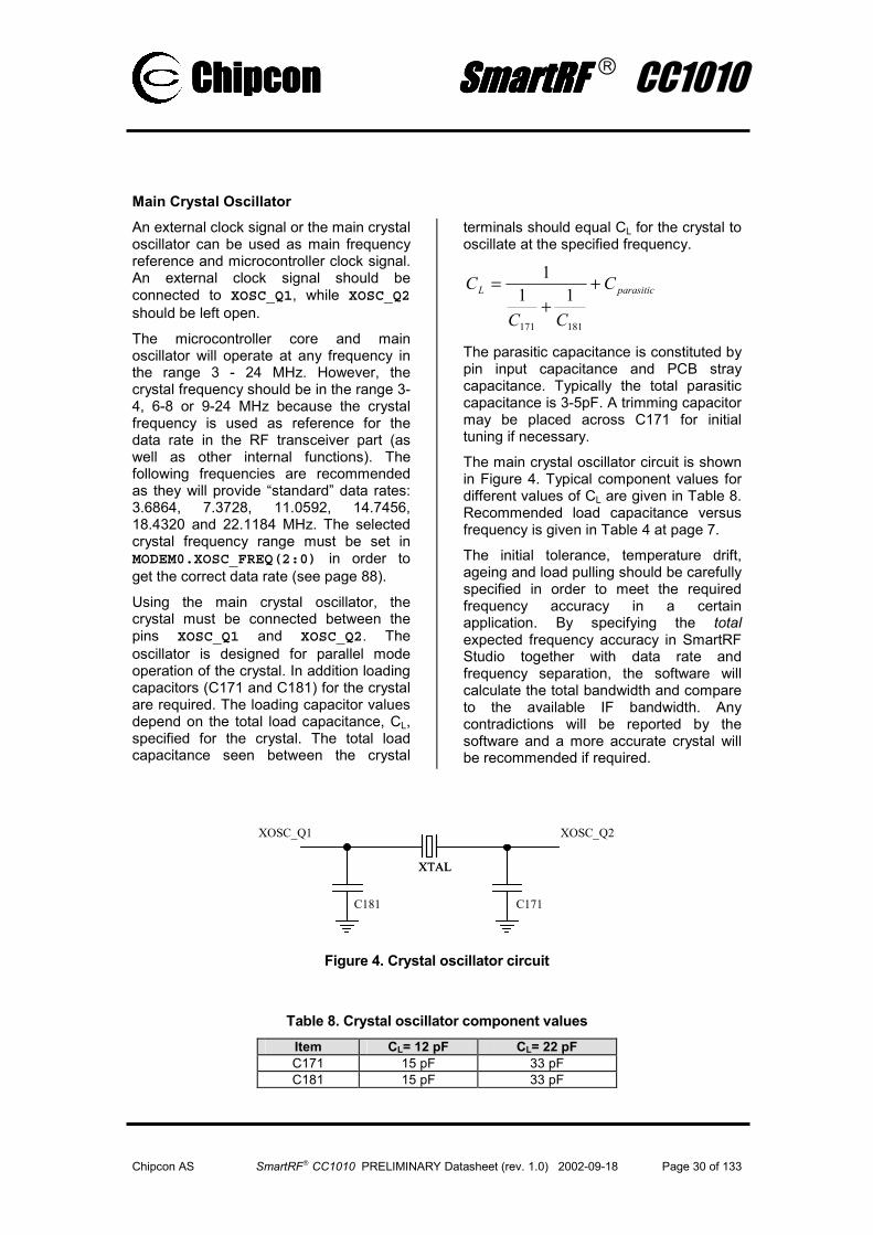
Main Crystal OscillatorAn external clock signal or the main crystal oscillator can be used as main frequency reference and microcontroller clock signal. An external clock signal should be connected to XOSC_Q1, while XOSC_Q2 should be left open.
The microcontroller core and main oscillator will operate at any frequency in the range 3 - 24 MHz. However, the crystal frequency should be in the range 3-4, 6-8 or 9-24 MHz because the crystal frequency is used as reference for the data rate in the RF transceiver part (as well as other internal functions). The following frequencies are recommended as they will provide “standard” data rates: 3.6864, 7.3728, 11.0592, 14.7456, 18.4320 and 22.1184 MHz. The selected crystal frequency range must be set in MODEM0.XOSC_FREQ(2:0) in order to get the correct data rate (see page 88).
Using the main crystal oscillator, the crystal must be connected between the pins XOSC_Q1 and XOSC_Q2. The oscillator is designed for parallel mode operation of the crystal. In addition loading capacitors (C171 and C181) for the crystal are required. The loading capacitor values depend on the total load capacitance, CL, specified for the crystal. The total load capacitance seen between the crystal
terminals should equal CL for the crystal to oscillate at the specified frequency.
parasiticL C
CC
C ++
=
181171
111
The parasitic capacitance is constituted by pin input capacitance and PCB stray capacitance. Typically the total parasitic capacitance is 3-5pF. A trimming capacitor may be placed across C171 for initial tuning if necessary.
The main crystal oscillator circuit is shown in Figure 4. Typical component values for different values of CL are given in Table 8. Recommended load capacitance versus frequency is given in Table 4 at page 7.
The initial tolerance, temperature drift, ageing and load pulling should be carefully specified in order to meet the required frequency accuracy in a certain application. By specifying the total expected frequency accuracy in SmartRF Studio together with data rate and frequency separation, the software will calculate the total bandwidth and compare to the available IF bandwidth. Any contradictions will be reported by the software and a more accurate crystal will be recommended if required.
C171C181
XTALXTAL
XOSC_Q1 XOSC_Q2
Figure 4. Crystal oscillator circuit
Table 8. Crystal oscillator component values
Item CL= 12 pF CL= 22 pF C171 15 pF 33 pF C181 15 pF 33 pF

ChipconChipconChipconChipcon SmartRF SmartRF SmartRF SmartRF CC1010
Chipcon AS SmartRF CC1010 PRELIMINARY Datasheet (rev. 1.0) 2002-09-18 Page 31 of 133
Power and Clock ModesSeveral power modes are defined to save power when running CC1010. The modes are described below. See also Table 9.
Active Mode
In active mode the 8051 is running normally, executing instructions from the Flash program memory. The clock used in this mode could either be the main crystal oscillator, or it could be the 32 kHz Real-time clock (RTC). The current consumption depends on the actual frequency used.
Idle Mode
After completing the instruction that sets the PCON.IDLE bit, Idle Mode is entered. In Idle Mode, the 8051 processing is stopped and internal registers maintain their current data, but all peripherals are still running.
There are 3 ways to exit Idle Mode:
• Activate any enabled interrupt. This clears the IDLE bit, terminating Idle Mode, and executes the ISR associated with the received interrupt. The RETI instruction at the end of the ISR causes the 8051 to return to the instruction following the one that enabled Idle Mode.
• Activate any reset condition. All registers are then reset, and program execution will resume from address
0x0000 when the reset condition is cleared.
• Turn the power off and on. The Power On Reset module should then be enabled, or an external reset signal should be applied during power up.
Power-Down Mode
After completing the instruction that sets the PCON.STOP bit, the controller core and the peripherals are stopped. In Power-Down Mode, the clock trees of the 8051 and peripherals are disabled. Only the ADC clock tree is running. This enables the ADC to generate reset as will be described in the ADC section.
There are 2 ways to exit Power Down Mode:
• Activate any reset condition. All registers are then reset, and program execution will resume when the reset condition is cleared. Program execution will then resume from address 0x0000.
• Turn the power off and on. The Power On Reset module should then be enabled, or an external reset signal should be applied during power up.
Table 9. Operating modes summary Mode Core Peripherals Typical current
consumption1 Exit condition
Main osc. Main osc. 10 mA at 11 MHz
Writing SFR
Active RTC osc. (32 kHz)
RTC osc. (32 kHz)
1.1 mA Writing SFR
Stopped Main osc. 8.5 mA at 11 MHz Idle Stopped RTC osc.
(32 kHz) 26 uA
Interrupt Reset Power off/on
Power-Down Stopped Stopped 0.2 uA Reset Power off/on
Note 1: Flash duty-cycle reduction is used for all modes
ChipconChipconChipconChipcon SmartRF SmartRF SmartRF SmartRF CC1010
Chipcon AS SmartRF CC1010 PRELIMINARY Datasheet (rev. 1.0) 2002-09-18 Page 32 of 133
Clock Modes
The 8051 and its peripherals can be run on both the main crystal oscillator (Clock Mode 0) and the 32.768 kHz oscillator (Clock Mode 1). The clock mode is set in X32CON.CMODE.
Entering Clock Mode 1 from Clock Mode 0
After reset, the 8051 and its peripherals are running on the main crystal oscillator, and the 32.768 kHz oscillator is in power down. To enter Clock Mode 1, the 32.768 kHz oscillator must first be powered up. This requires clearing X32CON.X32_PD and then waiting at least 160 ms, after which X32CON.CMODE can be set to enter Clock Mode 1.
If an external 32.768 kHz clock source is already available in the system, this clock can be applied to the XOSC32_Q1 pin after setting the X32CON.X32_BYPASS bit.
After 2 to 3 clock periods on the 32.768 kHz oscillator, a glitch free transition has been made from the main crystal oscillator to the 32.768 kHz oscillator. If desired, the main crystal oscillator can then be set in power down to save more power by setting RFMAIN.CORE_PD and RFMAIN.BIAS_PD. This has the disadvantage that a later transition from Clock Mode 1 to Clock Mode 0 will require
the main crystal oscillator to be powered up again,
Since the Flash program memory draws a static current, Idle Mode together with Flash Power Control (see page 40) should be applied for maximum power saving in Clock Mode 1.
RF communications cannot be performed in Clock Mode 1, since the 8051 and peripherals are running on the 32 kHz clock.
Entering Clock Mode 0 from Clock Mode 1
To enter Clock Mode 0 from Clock Mode 1, the main crystal oscillator must first be set in power up (if powered down). This requires clearing RFMAIN.CORE_PD and RFMAIN.BIAS_PD and then waiting at least 5 ms (depend on main oscillator frequency, see Electrical Specifications page 7). If the oscillator is already powered up, no waiting is required. Clearing X32CON.CMODE will then cause a glitch free transition from Clock Mode 1 to Clock Mode 0 after 2 to 3 clock periods on the main crystal oscillator.
Flash Power Control
The Flash program memory current consumption can be controlled as described in the Flash Power Control section on page 40.
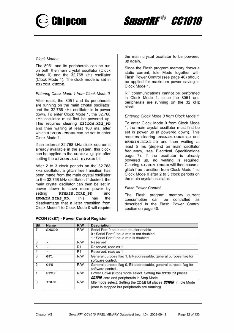
PCON (0x87) - Power Control Register Bit Name R/W Description 7 SMOD0 R/W Serial Port 0 baud rate doubler enable.
0 : Serial Port 0 baud rate is not doubled 1 : Serial Port 0 baud rate is doubled
6 - R/W Reserved 5 - R1 Reserved, read as 1 4 - R1 Reserved, read as 1 3 GF1 R/W General purpose flag 1. Bit-addressable, general purpose flag for
software control. 2 GF0 R/W General purpose flag 0. Bit-addressable, general purpose flag for
software control. 1 STOP R/W Power Down (Stop) mode select. Setting the STOP bit places
CC1010 core and peripherals in Stop Mode. 0 IDLE R/W Idle mode select. Setting the IDLE bit places CC1010 in Idle Mode
(core is stopped but peripherals are running).

ChipconChipconChipconChipcon SmartRF SmartRF SmartRF SmartRF CC1010
Chipcon AS SmartRF CC1010 PRELIMINARY Datasheet (rev. 1.0) 2002-09-18 Page 33 of 133
X32CON (0xD1) - 32.768 kHz Crystal Oscillator Control Register Bit Name R/W Description 7 - R0 Reserved, read as 0 6 - R0 Reserved, read as 0 5 - R0 Reserved, read as 0 4 - R0 Reserved, read as 0 3 - R0 Reserved, read as 0 2 X32_BYPASS R/W 32.768 kHz oscillator bypass control signal
0 : The internal 32.768 kHz oscillator is used to generate the 32.768kHz clock 1 : The internal 32.768 kHz oscillator is bypassed, and an external clock signal can be applied to the XOSC32_Q1 pin.
1 X32_PD R/W 32.768 kHz oscillator power down signal 0 : The oscillator is powered up (default after reset) 1 : The oscillator is powered down
0 CMODE R/W Select different Clock Modes for the 8051 and its peripherals. 0 : Clock Mode 0 is selected (default after reset) 1 : Clock Mode 1 is selected

ChipconChipconChipconChipcon SmartRF SmartRF SmartRF SmartRF CC1010
Chipcon AS SmartRF CC1010 PRELIMINARY Datasheet (rev. 1.0) 2002-09-18 Page 34 of 133
Flash Program Memory
CC1010 has 32 kBytes of on-chip Flash program memory. It is divided into 256 pages of 128 bytes each. It can be programmed / erased through a serial SPI interface or page-by-page from the 8051 as described in the following sections.
The endurance for the Flash program memory is typically 20.000 erase / write cycles.
The Flash program memory can be locked for further reading / writing by setting appropriate lock bits through the serial interface. Chip erase must be performed
to unlock the memory. This provides a way to prevent software from being copied by others. It can also prevent parts of the Flash memory from being modified by software, such as a boot loader which should remain unchanged. Other parts of the Flash may still be updated by the boot loader.
For the security of the Flash protection, please refer to the disclaimer at the end of this document.
SPI Flash ProgrammingThe on chip Flash program memory can be programmed using the SPI Flash programming protocol described in this section.
SPI Flash programming is enabled when the pin PROG is held low. This enables the SPI slave, using the pins SCK (P0.0) as the clock input, SI (P0.1) as the serial data input and SO (P0.2) as the serial data output.
A Windows based Flash programmer is also available free of charge at the Chipcon web site.
SPI Flash Programming Instructions
9 instructions are defined to perform the serial Flash programming. These are shown in Table 10.
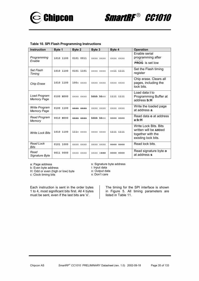
ChipconChipconChipconChipcon SmartRF SmartRF SmartRF SmartRF CC1010
Chipcon AS SmartRF CC1010 PRELIMINARY Datasheet (rev. 1.0) 2002-09-18 Page 35 of 133
Table 10. SPI Flash Programming Instructions Instruction Byte 1 Byte 2 Byte 3 Byte 4 Operation
Programming Enable
1010 1100 0101 0011 xxxx xxxx xxxx xxxx
Enable serial programming after PROG is set low
Set Flash Timing
1010 1100 0101 1101 xxxx xxxx xxii iiiiSet the Flash timing register
Chip Erase 1010 1100 100x xxxx xxxx xxxx xxxx xxxxChip erase. Clears all pages, including the lock bits.
Load Program Memory Page
0100 H000 xxxx xxxx bbbb bbxx iiii iiiiLoad data i to Programming Buffer at address b:H
Write Program Memory Page
0100 1100 aaaa aaaa xxxx xxxx xxxx xxxxWrite the loaded page at address a.
Read Program Memory
0010 H000 aaaa aaaa bbbb bbxx oooo ooooRead data o at address a:b:H
Write Lock Bits 1010 1100 111x xxxx xxxx xxxx iiii iiii
Write Lock Bits. Bits written will be ANDed together with the existing lock bits.
Read Lock Bits
0101 1000 xxxx xxxx xxxx xxxx oooo oooo Read lock bits.
Read Signature Byte
0011 0000 xxxx xxxx xxxx xsss oooo ooooRead signature byte o at address s
a: Page address b: Even byte address H: Odd or even (high or low) byte c: Clock timing bits
s: Signature byte address i: Input data o: Output data x: Don’t care
Each instruction is sent in the order bytes 1 to 4, most significant bits first. All 4 bytes must be sent, even if the last bits are 'x'.
The timing for the SPI interface is shown in Figure 5. All timing parameters are listed in Table 11.

ChipconChipconChipconChipcon SmartRF SmartRF SmartRF SmartRF CC1010
Chipcon AS SmartRF CC1010 PRELIMINARY Datasheet (rev. 1.0) 2002-09-18 Page 36 of 133
Figure 5. SPI Flash Programming Timing
Table 11. SPI Flash Programming Timing Parameters Symbol Min Max Units Conditions Fsck - fXOSC / 8 Tsck, high 4 ⋅ TXOSC - The minimum time SCK must be held high Tsck, low 4 ⋅ TXOSC - The minimum time SCK must be held low Tsck, rise - TXOSC /2 ns The maximum rise time on SCKTsck, fall - TXOSC /2 ns The maximum fall time on SCKTsi, setup TXOSC - The minimum setup time for SI before the positive edge
on SCKTsi, hold TXOSC - The minimum hold time for SI after the positive edge on
SCKTso, delay - TXOSC The delay from the negative edge on SCK to valid data
on SO
Programming Enable
Programming Enable is always the first instruction to be sent. It must be sent to synchronise the data flow and enable CC1010 to receive further instructions.
Synchronisation is achieved when byte 2 of the instruction (0x53) is echoed back from the SPI interface as byte 3. If synchronisation is not achieved, byte 3 will return all zeros. In this case, an extra clock pulse should be inserted on SCK, and the Programming Enable instruction should be resent. If synchronisation is not successful within 32 attempts, Programming Enable is unsuccessful and further debugging is needed.
Set Flash Timing
The Set Flash Timing instruction is needed to generate internal timing for the Flash
module. FLTIM must be set in instruction byte 4 so that:
MHzf
MHzf XOSCXOSC
4.08.0≤≤ FLTIM
It is recommended to set FLTIM to the smallest number satisfying the equation above, to reduce the time needed for Flash programming. For a 3.6864 MHz crystal, FLTIM should be set to 5.
Chip Erase
The Chip Erase instruction erases all data in the Flash memory, including the lock bits. All bits will be set high.
Wait 450 ms (depending on Set Flash Timing) after sending the Chip Erase instruction before issuing a new instruction.
SCK (P0.0)
SI (P0.1)
SO (P0.2)
7 6 5 4 3 2 1 0
7 6 5 4 3 2 1 0
Tsck, high Tsck, low Tsck, rise Tsck, fall
Tsi, setup Tsi, hold Tso, delay

ChipconChipconChipconChipcon SmartRF SmartRF SmartRF SmartRF CC1010
Chipcon AS SmartRF CC1010 PRELIMINARY Datasheet (rev. 1.0) 2002-09-18 Page 37 of 133
Load Program Memory Page
The Load Program Memory Page instruction is used to load the 128 bytes of data in a page to a buffer in RAM. Each instruction writes one byte to the 7 bit address specified in the instruction.
Write Program Memory Page
The Write Program Memory Page instruction writes the 128 bytes buffered through the Load Program Memory Page instructions to Flash memory.
After issuing this command, wait 5.4 ms for it to complete. It is also possible to use the Read Program Memory instruction to poll when the program memory has been written. When writing is in progress, all read instructions will return 0xFF. Reading an address containing data different from 0xFF can then be used to check when the write is completed.
Read Program Memory
The Flash program memory can be read back byte by byte using the Read Program Memory instruction. The data is returned in byte 4 of the instruction.
Wait at least 9 ⋅ TXOSC between the last negative transition on SCK for byte 3 before issuing the first positive edge on SCK for byte 4 to receive valid data.
Write Lock Bits
The reading (through SPI) and writing to the Flash program memory can be disabled by setting the lock bits as described in this section. This should be used for software protection.
The lock bits are set using the Write Lock Bits instruction. A block of programmable size at the top of the Flash program memory can be locked for writing using the LSIZE bits. Page 0 can be independently locked for writing by using the BBLOCK bit. Reading data through the SPI interface can be disabled using the SPIRE bit.
The detailed description of all lock bits are given in Table 12.
Table 12. Flash Lock Bits Bit Name Function 7:3 - Reserved, write as '0' 4 BBLOCK Boot Block Lock
0 : Page 0 is write protected 1 : Page 0 is writeable, unless LSIZE is 000
3 LSIZE.2 2 LSIZE.1 1 LSIZE.0
Lock Size, sets the size of the upper Flash area which is write protected. Byte sizes and page numbers are listed below: 000 : 32768 (All pages) 001 : 16384 (page 128-255) 010 : 8192 (page 192-255) 011 : 4096 (page 224-255) 100 : 2048 (page 240-255) 101 : 1024 (page 248-255) 110 : 512 (page 252-255) 111 : 0 (no pages)
0 SPIRE SPI Read Flash Enable / Disable 0 : SPI Interface returns all zeros on the Read Program Memory instruction 1 : SPI Interface returns valid Flash data on the Read Program Memory instruction
Lock bits can only be erased (set high) by issuing the Chip Erase instruction. If multiple Write Lock Bits instructions are issued without chip erase in between, each lock bit will be AND-ed together with the previously written lock bits.
In effect, this means that it is not possible to unlock the Flash program memory without also erasing it.
The effect of the different Flash write lock bits are illustrated in Figure 6.

ChipconChipconChipconChipcon SmartRF SmartRF SmartRF SmartRF CC1010
Chipcon AS SmartRF CC1010 PRELIMINARY Datasheet (rev. 1.0) 2002-09-18 Page 38 of 133
012
126127128129130
190191192193194
222223224225226
238239240241242
246247248249250251252253254255
Pag
e nu
mbe
r
Add
ress
0x7FFF
0x7E00
0x7C00
0x7800
0x7000
0x6000
0x4000
0x0000
LSIZ
E =
000
LOC
KED
LOC
KED
UN
LOC
KED
LOC
KED
UN
LOC
KED
LOC
KED
UN
LOC
KED
LOC
KED
UN
LOC
KED
UN
LOC
KED
LOC
KED
LOC
KED
LSIZ
E =
001
LSIZ
E =
010
LSIZ
E =
011
LSIZ
E =
100
LSIZ
E =
101
LSIZ
E =
110
LSIZ
E =
111
UN
LOC
KED
UN
LOC
KED
Page 0 is locked when BBLOCK is cleared
Figure 6. Flash Lock Bits illustration
Read Lock Bits
The lock bits described in the previous section can be read through the SPI interface by using the Read Lock Bits instruction. The instruction will return the 8 lock bits in byte 4 of the instruction.
Wait at least 9 ⋅ TXOSC between the last negative transition on SCK for byte 3 before issuing the first positive edge on SCK for byte 4 to receive valid data, as with the Read Program Memory instruction.
The lock bits can only be read through the SPI interface, and not from the 8051 core.
Read Signature Byte
A 6 byte chip signature can be read through the SPI interface using the Read
Signature Byte instruction. The 3 bit signature byte address is issued, and the value is then returned as byte 4.
Table 13. Signature Bytes Signature byte address Value Meaing 000 0x7F 001 0x7F 010 0x7F 011 0x9E
JEDEC manufacturer ID, identifies Chipcon AS as the manufacturer.
100 0x95 Identifies 32 kBytes of Flash memory
101 0x00 Identifies CC1010
Wait at least 9 ⋅ TXOSC between the last negative transition on SCK for byte 3 before issuing the first positive edge on SCK for byte 4 to receive valid data, as with the Read Program Memory instruction.
SPI Flash Programming Initialisation
CC1010 must be set into the Flash programming mode to allow SPI Flash operations. This is done as follows:
• Apply power between all DVDD and DGND pins.
• Hold PROG low
• If a crystal is connected between XOSC_Q1 and XOSC_Q2, hold RESET low and wait for the oscillator to start up. Crystal oscillator start-up times are given in Table 4. Release RESET and wait at least 4 crystal oscillator periods.
• If a crystal is not connected between XOSC_Q1 and XOSC_Q2, hold RESET low and apply a clock signal to XOSC_Q1. Release RESET after at least 3 clock periods, and then wait at least 4 clock periods.
• Execute the Programming Enable instruction to complete the SPI Flash programming Initialisation.
ChipconChipconChipconChipcon SmartRF SmartRF SmartRF SmartRF CC1010
Chipcon AS SmartRF CC1010 PRELIMINARY Datasheet (rev. 1.0) 2002-09-18 Page 39 of 133
CC1010 is now ready to be programmed, as described in the next section.
Programming the Flash Memory
After the initialisation is completed, SPI programming can be performed as follows:
• Device identity can be verified using the Read Signature Byte instruction.
• Perform Chip Erase.
• Load one page into the buffer using the Load Program Memory Page instruction.
• Write the buffer to Flash by using the Write Program Memory Page instruction.
• Repeat the loading and writing of each new page.
• Programming can be verified using the Read Program Memory instruction.
• Set the lock bits using the Write Lock Bits instruction.
• Lock bits can be verified by using the Read Lock Bits instruction.
8051 Flash Programming Each of the 256 pages (128 bytes each) in Flash program memory can be programmed individually from the 8051. The 8051 must be set in Idle Mode while programming the Flash, since it has no access to the program memory while the writing is in progress. The step for writing a page to Flash is described as follows:
• Set the correct write cycle time, according to the current crystal oscillator frequency, in the FLTIM SFR. This number is used to generate the timing to the on-chip Flash interface, as was also done with SPI Flash programming. It must be set so that:
MHzf
MHzf XOSCXOSC
4.08.0≤≤ FLTIM
• The time used for programming a Flash page is strongly dependent on the setting in FLTIM. It is therefore recommended to set FLTIM as low as possible, as with the SPI Flash programming.
• Write the desired Flash page number to the FLADR register.
• Disable all interrupts except the Flash / Debug interrupt, which must be enabled (through EICON.FDIE)
• Store the 128 bytes of data to be written in the external data memory. The address of the first byte in the bufffer must be a multiple of 128.
• Write the 4 most significant bits of the RAM buffer address to FLCON.RMADR(3:0). Also set the bit FLCON.WRFLASH
• Set the 8051 in Idle Mode by setting PCON.IDLE. The Flash page is then autmatically erased and programmed.
The sequence of the above steps are not important. Flash programming is started whenever entering Idle Mode while FLCON.WRFLASH is set.
A Flash / Debug interrupt will be generated when the page write operation is completed, which will get the 8051 out of Idle Mode. An ISR must be present to service the Flash / Debug interrupt.
FLADR (0xAE) - Flash Write Address RegisterBit Name R/W Description 7:0 FLADR(7:0) R/W The number of of the Flash page to be written (8 MSB of the byte
address)

ChipconChipconChipconChipcon SmartRF SmartRF SmartRF SmartRF CC1010
Chipcon AS SmartRF CC1010 PRELIMINARY Datasheet (rev. 1.0) 2002-09-18 Page 40 of 133
FLCON (0xAF) - Flash Write Control RegisterBit Name R/W Description 7 - R0 Reserved, read as 0 6:5 FLASH_LP
(1:0)R/W Flash Low Power control bits
00 : The Flash module is always active. 01 : The Flash module enters standby mode when the 8051 is put in Idle mode or Stop mode 10 : The Flash module enters standby mode between instruction fetches and when the 8051 is put in Idle Mode or Stop Mode. 11 : Reserved for future use.
4 WRFLASH R/W Write Flash Start bit Starting a Flash page programming is done by first setting this bit and then setting the 8051 in Idle Mode. If the WRFLASH bit is cleared before Idle Mode is entered, no programming is performed.
3:0 RMADR(3:0) R/W RAM Buffer address RMADR(3:0) contains the 4 most significant bits of the RAM address where the data is buffered before writing to Flash
FLTIM (0xDD) - Flash Write Timing RegisterBit Name R/W Description 7:0 FLTIM(7:0) R/W Flash Write Timing control
FLTIM must be set as described in this section prior to using the 8051 Flash programming.
If an attempt is made to write data to a Flash page which is locked (see the previous section), a Flash / Debug interrupt will be generated immediately after Idle Mode is entered. No data will be written.
It is not possible to read or write the Flash lock bits from the 8051.
Example Code
An example code writing data buffered at address 0x100-0x17F in external RAM to the second page in Flash (address 0x080-0x0FF) is shown below.The system clock frequency is assumed to be 3.6864 MHz.
An interrupt service routine must be present at address 0x33, which clears the interrupt flag EICON.FDIF and returns from the interrupt (RETI).
FLTIM=0x05; /* Set Flash timing for 3.6864 MHz clock frequency */FLADR=0x01; /* Write data to the second page in Flash */EICON|=0x20; /* Enable Flash interrupt */IE&= ~0x80; /* Disable other interrupts */FLCON=0x10 | (0x100 >> 7);
/* Enable Flash writing, RAM buffer from addr. 0x100 */PCON|=0x01; /* Enter Idle Mode to start Flash writing.
Flash Power Control The Flash module can be set into different power modes using the control bits FLCON.FLASH_LP(1:0) introduced in the previous section.
After reset, the Flash module is always active, drawing a static current of
approximately 2.5 mA (at nominal operating conditions). However, to save power the Flash module can be set in a power-down mode between instructions in Active mode, and always in Idle or Power-Down mode. This will save approximately

ChipconChipconChipconChipcon SmartRF SmartRF SmartRF SmartRF CC1010
Chipcon AS SmartRF CC1010 PRELIMINARY Datasheet (rev. 1.0) 2002-09-18 Page 41 of 133
1.5 mA of the Flash current consumption during operation in Active mode, and 2.5
mA during Idle or Power-Down mode.
In Circuit DebuggingIn order to facilitate a software monitor for in-circuit debugging/emulation capabilities a number of hardware support features have been implemented:
A breakpoint instruction has been added to the 8051's instruction set. The instruction, given the mnemonic TRAP, is a single byte instruction with the opcode 0xA5. In the original 8051 the 0xA5 opcode executed as a NOP instruction (opcode 0x00.) In the modified core this instruction raises a highest-level interrupt (Flash / Debug) by setting the corresponding interrupt flag EICON.FDIF and waiting a sufficient number of instruction cycles to allow the interrupt to take effect before the next instruction.
The TRAP instruction can thus be written over the first byte (opcode) of any other instruction, the execution of which then will result in a branch to a software debugging monitor in the highest priority interrupt service routine.
Single-stepping through instructions is supported since exactly one instruction is executed if an interrupt condition exists when returning from an interrupt service routine. Thus, single-stepping can be accomplished simply by not clearing the corresponding interrupt flag in the interrupt service routine associated with the software monitor.
A second serial port has been added to enable debugging communication with a host PC without disrupting applications who use the main serial port for other purposes.
Setting breakpoints and executing the instructions which have a breakpoint attached involves writing new data to the Flash instruction memory several times. Since the Flash memory can only withstand 20000 (typical) erase/write-cycles a simple instruction replacement mechanism has been implemented. This
feature allows the surveillance of an address in the instruction memory space as defined in registers RADRL and RADRH. When this address is encountered on the Flash program memory address bus, the data returned on the data bus is replaced by the contents of register RDATA. Setting RADRH=RADRL=0 disables the replacement mechanism.
This instruction replacement mechanism can be used in different ways:
• A simple way of setting a single soft (not stored in FLASH) breakpoint, by setting RDATA to 0xA5 (the TRAP instruction) and RADR to the breakpoint address.
• A simple way of restoring the original opcode byte of an instruction which has been subjected to a hard (stored in Flash) breakpoint, so that it can be executed (in single-step mode).
• SFRs (hardware registers) can normally only be addressed directly (i.e. by hardwiring the specific address into the corresponding MOV instruction.) This would make code in a debug monitor, which returns the value of SFRs to a PC rather bloated. Using the instruction replacement mechanism on the operand byte of the move instruction instead of the opcode byte, allows indirect addressing of SFRs.
Chipcon provides software for in-circuit debugging, which may be downloaded from the Chipcon homepage. This software uses the RESERVED register, which can then not be used for other purposes. If in-circuit debugging is not required, the RESERVED register shown below may be used for any purpose. Writing to it will have no effect on the operation of CC1010.
ChipconChipconChipconChipcon SmartRF SmartRF SmartRF SmartRF CC1010
Chipcon AS SmartRF CC1010 PRELIMINARY Datasheet (rev. 1.0) 2002-09-18 Page 42 of 133
Great caution should be used when the RADR is written. As the address consist of two bytes (RADRL and RADRH) there will be a short interval where the address is not valid as only one of the bytes are written at a time. If this intermediate
address point to the very same location as of the code modifying the RADR, a malfunction will occur. One possible work-around is to first write RADRH to a value pointing to a memory location not used by the code.
RESERVED (0xE7) - Reserved register, used by Chipcon debugger software Bit Name R/W Description 7:0 RESERVED(7:0) R/W Reserve register, which is used by Chipcon debugger software.
RESERVED may be used for other purposes if Chipcons debugger software is not needed.
RDATA (0xB9) - Replacement Data Bit Name R/W Description 7:0 RDATA(7:0) R/W Replacement data.
Used to replace the byte at program memory address RADR with the data from RDATA, if RADR > 0.
RADRH (0xBB) - Replacement address, high byte Bit Name R/W Description 7:0 RADR(15:8) R/W Replacement address, high byte.
Used to replace the byte at program memory address RADR with the data from RDATA, if RADR > 0.
RADRL (0xBA) - Replacement address, low byte Bit Name R/W Description 7:0 RADR(7:0) R/W Replacement address, low byte.
Used to replace the byte at program memory address RADR with the data from RDATA, if RADR > 0
Chip Version / Revision
CC1010 has a SFR register CHVER which can be read to decide the chip type and
current revision. The register description is shown below.
CHVER (0x9F) - Chip Version / Revision Register Bit Name R/W Description 7:2 CHIP_TYPE R CHIP_TYPE is a read only status word, which gives the type
number of the chip. 000000 : CC1010 000001 - 111111 : Reserved for future use
1:0 CHIP_REV R CHIP_REV is a read only status word, which gives the chip revision number of the chip. Current chip revision is 01

ChipconChipconChipconChipcon SmartRF SmartRF SmartRF SmartRF CC1010
Chipcon AS SmartRF CC1010 PRELIMINARY Datasheet (rev. 1.0) 2002-09-18 Page 43 of 133
8051 Peripherals CC1010 offers the following peripherals units controlled by the 8051 core:
• Four general purpose I/O ports, with a total of 26 I/O pins.
• Two standard 8051 timers
• Two timers with PWM functionality
• Watchdog timer
• Realtime clock
• SPI master
• Hardware DES encryption / decryption
• Random bit generator
• 10 bit ADC
These modules are described in the following sections.
General Purpose I/O Four general purpose I/O-ports are available: P0, P1, P2 and P3. Table 5 shows each port and the pins on each port.
Each port is associated with two registers: The port register (P0, P1, P2, or P3) and the direction register (P0DIR, P1DIR, P2DIR, or P3DIR).
Each bit in the Px registers has its associated bit in the direction registers PxDIR. Setting PxDIR.y will make Px.y an input which can be read in Px(y). All pins are inputs after reset. Clearing PxDIR.y will make the pin Px.y output the data from the register Px(y). All Px and PxDIR register descriptions are shown from page 45.
The structure for a single I/O-bit y on port x is shown in Figure 7. Some ports have alternate functions (such as the SPI interface), which are enabled through other registers (such as SPCR.SPE). These alternate functions may or may not override the direction setting from PxDIR
as shown. When reading the Px registers, data is read from the pad. When using a read-modify-write instruction such as ANL Px, #0x01, the output register value is read and modified regardless of the setting in PxDIR.
The CC1010 ports deviate from the standard 8051-port in the following ways:
• No pull ups / pull downs on pins
• Dedicated direction bits in PxDIR registers
• CMOS output on all ports
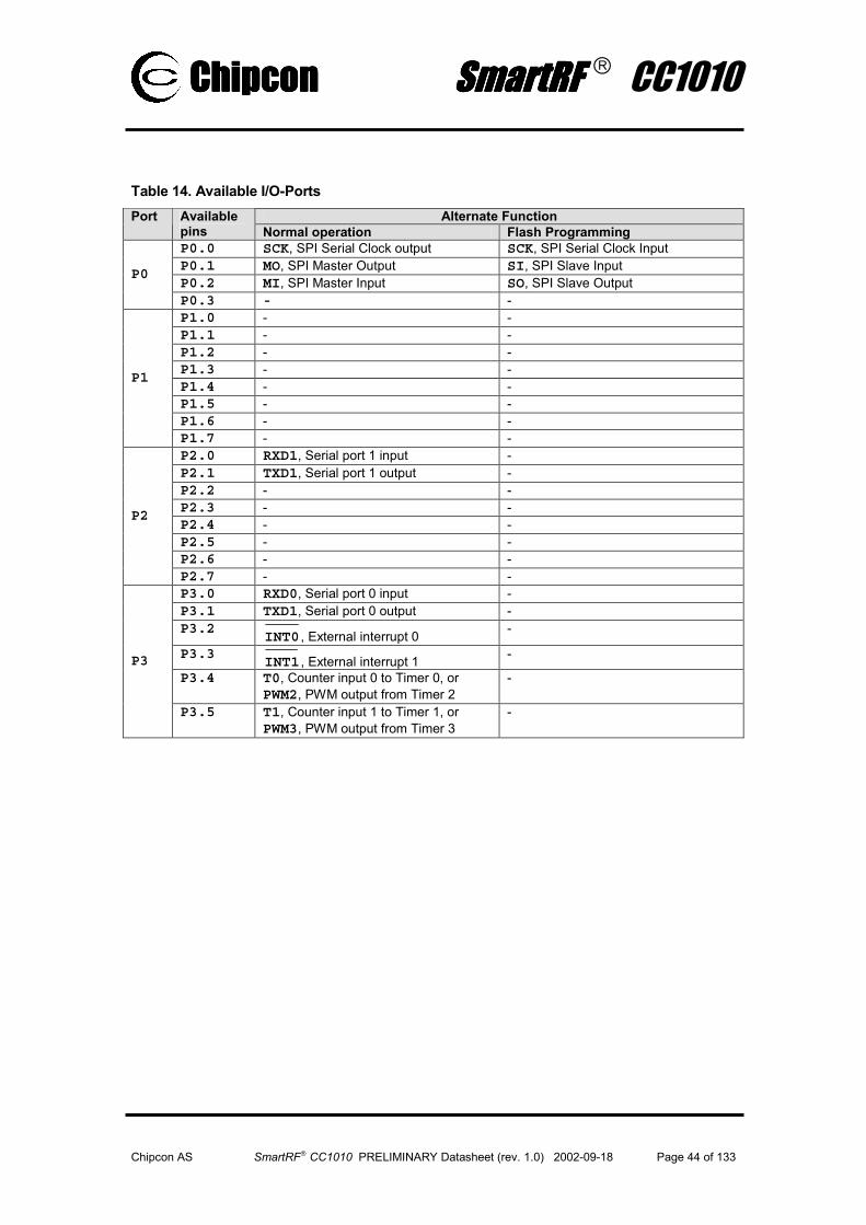
ChipconChipconChipconChipcon SmartRF SmartRF SmartRF SmartRF CC1010
Chipcon AS SmartRF CC1010 PRELIMINARY Datasheet (rev. 1.0) 2002-09-18 Page 44 of 133
Table 14. Available I/O-Ports Alternate Function Port Available
pins Normal operation Flash Programming P0.0 SCK, SPI Serial Clock output SCK, SPI Serial Clock Input P0.1 MO, SPI Master Output SI, SPI Slave Input P0.2 MI, SPI Master Input SO, SPI Slave Output
P0
P0.3 - - P1.0 - - P1.1 - - P1.2 - - P1.3 - - P1.4 - - P1.5 - - P1.6 - -
P1
P1.7 - - P2.0 RXD1, Serial port 1 input - P2.1 TXD1, Serial port 1 output - P2.2 - - P2.3 - - P2.4 - - P2.5 - - P2.6 - -
P2
P2.7 - - P3.0 RXD0, Serial port 0 input - P3.1 TXD1, Serial port 0 output - P3.2
INT0 , External interrupt 0 -
P3.3INT1 , External interrupt 1 -
P3.4 T0, Counter input 0 to Timer 0, or PWM2, PWM output from Timer 2
- P3
P3.5 T1, Counter input 1 to Timer 1, or PWM3, PWM output from Timer 3
-

ChipconChipconChipconChipcon SmartRF SmartRF SmartRF SmartRF CC1010
Chipcon AS SmartRF CC1010 PRELIMINARY Datasheet (rev. 1.0) 2002-09-18 Page 45 of 133
Figure 7. Port x bit y structure
P0 (0x80) - Port 0 Data Register Bit Name R/W Description 7 - R0 Reserved, read as 0 6 - R0 Reserved, read as 0 5 - R0 Reserved, read as 0 4 - R0 Reserved, read as 0 3 P0_3 R/W 2 P0_2 R/W 1 P0_1 R/W 0 P0_0 R/W
Data of port 0, bits 0 to 3.
P1 (0x90) - Port 1 Data Register Bit Name R/W Description 7 P1_7 R/W 6 P1_6 R/W 5 P1_5 R/W 4 P1_4 R/W 3 P1_3 R/W 2 P1_2 R/W 1 P1_1 R/W 0 P1_0 R/W
Data of port 1, bits 0 to 7.
Alternate function enable
Alternate function staticdirection or PxDIR.y
Alternate data
Read output register enable
PxDIR.y
D QInternal Data Bus
Read Pin Enable
S1
0
S1
0Px.y PAD
Output register

ChipconChipconChipconChipcon SmartRF SmartRF SmartRF SmartRF CC1010
Chipcon AS SmartRF CC1010 PRELIMINARY Datasheet (rev. 1.0) 2002-09-18 Page 46 of 133
P2 (0xA0) - Port 2 Data Register Bit Name R/W Description 7 P2_7 R/W 6 P2_6 R/W 5 P2_5 R/W 4 P2_4 R/W 3 P2_3 R/W 2 P2_2 R/W 1 P2_1 R/W 0 P2_0 R/W
Data of port 2, bits 0 to 7
P3 (0xB0) - Port 3 Data Register Bit Name R/W Description 7 - R0 Reserved, read as 0 6 - R0 Reserved, read as 0 5 P3_5 R/W 4 P3_4 R/W 3 P3_3 R/W 2 P3_2 R/W 1 P3_1 R/W 0 P3_0 R/W
Data of port 3, bits 0 to 5
P0DIR (0xA4) - Port 0 Direction Register Bit Name R/W Description 7 - R0 Reserved, read as 0 6 - R0 Reserved, read as 0 5 - R0 Reserved, read as 0 4 - R0 Reserved, read as 0 3 P0DIR_3 R/W 2 P0DIR_2 R/W 1 P0DIR_1 R/W 0 P0DIR_0 R/W
Port 0 direction register, bit 0 to 3. Each bit sets the direction of the associated pin on Port 0. 0 : Associated pin is an output 1 : Associated pin is an input
P1DIR (0xA5) - Port 1 Direction Register Bit Name R/W Description 7 P1DIR_7 R/W 6 P1DIR_6 R/W 5 P1DIR_5 R/W 4 P1DIR_4 R/W 3 P1DIR_3 R/W 2 P1DIR_2 R/W 1 P1DIR_1 R/W 0 P1DIR_0 R/W
Port 1 direction register, bit 0 to 7. Each bit sets the direction of the associated pin on Port 1. 0 : Associated pin is an output 1 : Associated pin is an input

ChipconChipconChipconChipcon SmartRF SmartRF SmartRF SmartRF CC1010
Chipcon AS SmartRF CC1010 PRELIMINARY Datasheet (rev. 1.0) 2002-09-18 Page 47 of 133
P2DIR (0xA6) - Port 2 Direction Register Bit Name R/W Description 7 P2DIR_7 R/W 6 P2DIR_6 R/W 5 P2DIR_5 R/W 4 P2DIR_4 R/W 3 P2DIR_3 R/W 2 P2DIR_2 R/W 1 P2DIR_1 R/W 0 P2DIR_0 R/W
Port 2 direction register, bit 0 to 7. Each bit sets the direction of the associated pin on Port 2. 0 : Associated pin is an output 1 : Associated pin is an input
P3DIR (0xA7) - Port 3 Direction Register Bit Name R/W Description 7 - R0 Reserved, read as 0 6 - R0 Reserved, read as 0 5 P3DIR_5 R/W 4 P3DIR_4 R/W 3 P3DIR_3 R/W 2 P3DIR_2 R/W 1 P3DIR_1 R/W 0 P3DIR_0 R/W
Port 3 direction register, bit 0 to 7. Each bit sets the direction of the associated pin on Port 3. 0 : Associated pin is an output 1 : Associated pin is an input
ChipconChipconChipconChipcon SmartRF SmartRF SmartRF SmartRF CC1010
Chipcon AS SmartRF CC1010 PRELIMINARY Datasheet (rev. 1.0) 2002-09-18 Page 48 of 133
Timer 0 / Timer 1
CC1010 contains two standard 8051 timers/counters (Timer 0 and Timer 1) which can operate as either a timer with a clock rate based on the system clock (as defined by the current clock mode), or as an event counter clocked by the T0 (P3.4 for Timer 0) or T1 (P3.5 for Timer 1) inputs.
Each Timer / Counter has a 16-bit register which is readable and writeable through TL0 and TH0 for Timer / Counter 0 and TL1 and TH1 for Timer / Counter 1. These registers are described below.
TL0 (0x8A) - Timer / Counter 0 Low byte counter value Bit Name R/W Description 7:0 TL0(7:0) R/W Timer / Counter 0, low byte counter value
TL1 (0x8B) - Timer / Counter 1 Low byte counter value Bit Name R/W Description 7:0 TL1(7:0) R/W Timer / Counter 1, low byte counter value
TH0 (0x8C) - Timer / Counter 0 High byte counter value Bit Name R/W Description 7:0 TH0(7:0) R/W Timer / Counter 0, high byte counter value
TH1 (0x8D) - Timer / Counter 1 High byte counter value Bit Name R/W Description 7:0 TH1(7:0) R/W Timer / Counter 1, high byte counter value
Timer / Counter 0 and 1 Modes
Timer / Counter 0 and 1 can individually be programmed to operate in one out of four different modes, controllable through the registers TMOD and TCON. They are as follows:
• 13-bit timer / counter (Mode 0)
• 16-bit timer / counter (Mode 1)
• 8-bit timer / counter with auto-reload (Mode 2)
• Two 8-bit timers / counters (Mode 3, Timer 0 only)
See the register descriptions for TMOD and TCON on the following pages.
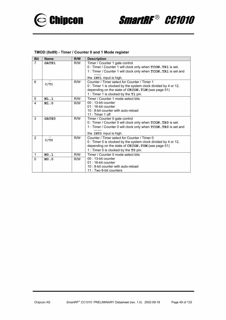
ChipconChipconChipconChipcon SmartRF SmartRF SmartRF SmartRF CC1010
Chipcon AS SmartRF CC1010 PRELIMINARY Datasheet (rev. 1.0) 2002-09-18 Page 49 of 133
TMOD (0x89) - Timer / Counter 0 and 1 Mode register Bit Name R/W Description 7 GATE1 R/W Timer / Counter 1 gate control
0 : Timer / Counter 1 will clock only when TCON.TR1 is set. 1 : Timer / Counter 1 will clock only when TCON.TR1 is set and
the INT1 input is high. 6
1TC/R/W Counter / Timer select for Counter / Timer 1
0 : Timer 1 is clocked by the system clock divided by 4 or 12, depending on the state of CKCON.T1M (see page 51) 1 : Timer 1 is clocked by the T1 pin.
5 M1.1 R/W 4 M1.0 R/W
Timer / Counter 1 mode select bits 00 : 13-bit counter 01 : 16-bit counter 10 : 8-bit counter with auto-reload 11 : Timer 1 off
3 GATE0 R/W Timer / Counter 0 gate control 0 : Timer / Counter 0 will clock only when TCON.TR0 is set. 1 : Timer / Counter 0 will clock only when TCON.TR0 is set and
the INT0 input is high. 2
0TC/R/W Counter / Timer select for Counter / Timer 0
0 : Timer 0 is clocked by the system clock divided by 4 or 12, depending on the state of CKCON.T0M (see page 51) 1 : Timer 0 is clocked by the T0 pin.
1 M0.1 R/W 0 M0.0 R/W
Timer / Counter 0 mode select bits 00 : 13-bit counter 01 : 16-bit counter 10 : 8-bit counter with auto-reload 11 : Two 8-bit counters

ChipconChipconChipconChipcon SmartRF SmartRF SmartRF SmartRF CC1010
Chipcon AS SmartRF CC1010 PRELIMINARY Datasheet (rev. 1.0) 2002-09-18 Page 50 of 133
TCON (0x88) - Timer / Counter 0 and 1 control register Bit Name R/W Description 7 TF1 R/W Timer 1 overflow flag. TF1 is set to 1 by hardware when the Timer
1 count overflows and is cleared by hardware when the 8051 vectors to the interrupt service routine.
6 TR1 R/W Timer 1 run control bit 0 : Timer / Counter 1 is disabled 1 : Timer / Counter 1 is enabled
5 TF0 R/W Timer 0 overflow flag. TF0 is set to 1 by hardware when the Timer 0 count overflows and is cleared by hardware when the 8051 vectors to the interrupt service routine.
4 TR0 R/W Timer 0 run control bit 0 : Timer / Counter 0 is disabled 1 : Timer / Counter 0 is enabled
3 IE1 R/W0 External interrupt 1 edge detect (interrupt flag) If external interrupt 1 is configured to be edge sensitive (TCON.IT1 = 1), IE1 is set by hardware when a negative edge
is detected on the INT1 pin and is cleared by hardware when the 8051 vectors to the corresponding interrupt service routine. In edge-sensitive mode, IE1 can also be set by software. If external interrupt 1 is configured to be level-sensitive
(TCON.IT1 = 0), IE1 is set when the INT1 pin is low and
cleared when the INT1 pin is high. In level-sensitive mode, software cannot write to IE1.
2 IT1 R/W External interrupt 1 type select.
0 : The INT1 interrupt is triggered when INT1 is low (level sensitive).
1 : The INT1 interrupt is triggered on the falling edge (edge sensitive)
1 IE0 R/W0 External interrupt 0 edge detect (interrupt flag) If external interrupt 0 is configured to be edge sensitive (TCON.IT0 = 1), IE0 is set by hardware when a negative edge
is detected on the INT0 pin and is cleared by hardware when the 8051 vectors to the corresponding interrupt service routine. In edge-sensitive mode, IE0 can also be set by software. If external interrupt 0 is configured to be level-sensitive
(TCON.IT0 = 0), IE0 is set when the INT0 pin is low and
cleared when the INT0 pin is high. In level-sensitive mode, software cannot write to IE0.
0 IT0 R/W External interrupt 0 type select.
0 : The INT0 interrupt is triggered when INT0 is low (level sensitive).
1 : The INT0 interrupt is triggered on the falling edge (edge sensitive)
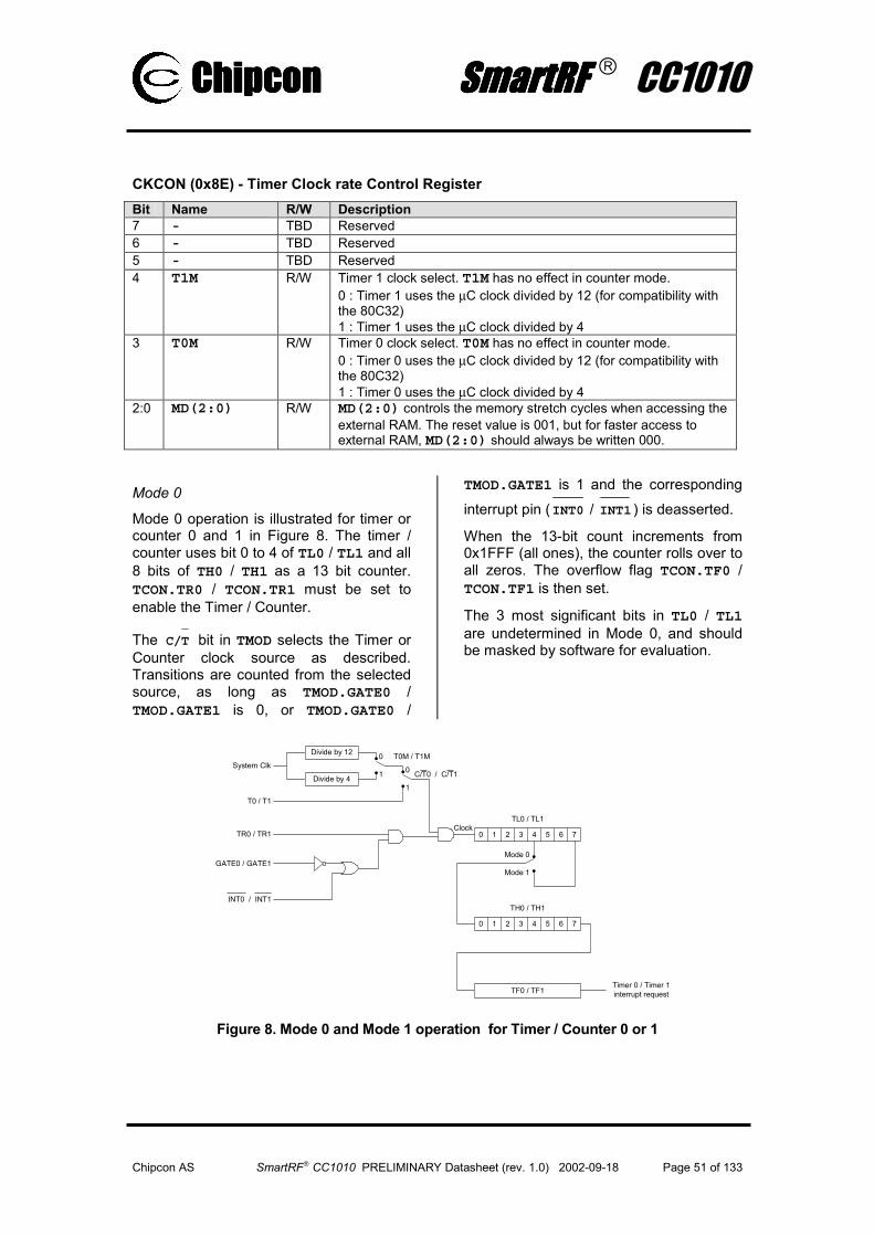
ChipconChipconChipconChipcon SmartRF SmartRF SmartRF SmartRF CC1010
Chipcon AS SmartRF CC1010 PRELIMINARY Datasheet (rev. 1.0) 2002-09-18 Page 51 of 133
CKCON (0x8E) - Timer Clock rate Control Register Bit Name R/W Description 7 - TBD Reserved 6 - TBD Reserved 5 - TBD Reserved 4 T1M R/W Timer 1 clock select. T1M has no effect in counter mode.
0 : Timer 1 uses the µC clock divided by 12 (for compatibility with the 80C32) 1 : Timer 1 uses the µC clock divided by 4
3 T0M R/W Timer 0 clock select. T0M has no effect in counter mode. 0 : Timer 0 uses the µC clock divided by 12 (for compatibility with the 80C32) 1 : Timer 0 uses the µC clock divided by 4
2:0 MD(2:0) R/W MD(2:0) controls the memory stretch cycles when accessing the external RAM. The reset value is 001, but for faster access to external RAM, MD(2:0) should always be written 000.
Mode 0
Mode 0 operation is illustrated for timer or counter 0 and 1 in Figure 8. The timer / counter uses bit 0 to 4 of TL0 / TL1 and all 8 bits of TH0 / TH1 as a 13 bit counter. TCON.TR0 / TCON.TR1 must be set to enable the Timer / Counter.
The TC/ bit in TMOD selects the Timer or Counter clock source as described. Transitions are counted from the selected source, as long as TMOD.GATE0 / TMOD.GATE1 is 0, or TMOD.GATE0 /
TMOD.GATE1 is 1 and the corresponding interrupt pin (INT0 / INT1 ) is deasserted.
When the 13-bit count increments from 0x1FFF (all ones), the counter rolls over to all zeros. The overflow flag TCON.TF0 / TCON.TF1 is then set.
The 3 most significant bits in TL0 / TL1 are undetermined in Mode 0, and should be masked by software for evaluation.
System Clk
Divide by 12
Divide by 4
0
1
T0 / T1
T0M / T1M
0
1
C/T0 / C/T1
TR0 / TR1
GATE0 / GATE1
INT0 / INT1
TL0 / TL1
0 1 2 3 4 5 6 7
TH0 / TH1
0 1 2 3 4 5 6 7
Mode 0
Mode 1
TF0 / TF1Timer 0 / Timer 1interrupt request
Clock
Figure 8. Mode 0 and Mode 1 operation for Timer / Counter 0 or 1

ChipconChipconChipconChipcon SmartRF SmartRF SmartRF SmartRF CC1010
Chipcon AS SmartRF CC1010 PRELIMINARY Datasheet (rev. 1.0) 2002-09-18 Page 52 of 133
Mode 1
Mode 1 operation is illustrated for Timer / Counter 0 and 1 in Figure 8. The counter is configured as a 16 bit counter, as compared to the 13 bits in Mode 0, and all bits in TL0 or TL1 are thus used. The counter overflows when the count increments from 0xFFFF.
Otherwise, Mode 1 operation is the same as Mode 0.
Mode 2
Mode 2 operation is illustrated for Timer / Counter 0 and 1 in Figure 9. Mode 2 operates as an 8 bit counter with automatic reload of the start value.
The Timer / Counter is controlled as for Mode 0 and Mode 1, but when TL0 / TL1 overflows, TH0 / TH1 is loaded into TL0 / TL1.
System Clk
Divide by 12
Divide by 4
0
1
T0 / T1
T0M / T1M
0
1
C/T0 / C/T1
TR0 / TR1
GATE0 / GATE1
INT0 / INT1
TL0 / TL1
TH0 / TH1
TF0 / TF1Timer 0 / Timer 1interrupt request
Clock
Mux
Reload
Figure 9. Mode 2 operation for Timer / Counter 0 or 1
Mode 3
In Mode 3, which is illustrated in Figure 10, Timer 0 is operated as two separate 8-bit counters and Timer 1 stops counting and holds its value.
TL0 is configured as an 8 bit counter controlled by the normal Timer 0 control bits. It counts either clock cycles divided by 4 or by 12 (as given by CKCON.T0M), or high to low transitions on T0 (as given by
0TTMOD.C/ ). It is also possible to use the
GATE function for TL0 to set INT0 as count enable.
TH0 is locked into a timer function, and takes over the use of TR1 and TF1 from Timer 1. It counts clock cycles divided by 4
or 12 (as given by CKCON.T1M). TH0 may then generate Timer 1 interrupts.
Timer 1 has limited usage when Timer 0 is in mode 3. This is because Timer 0 uses the Timer 1 control bit TR1 and the interrupt flag TF1. However, Timer 1 can still be used for baud rate generation and the Timer 1 count values are still available in the TL1 and TH1 registers.
Control of Timer 1 when Timer 0 is in mode 3 is done through the Timer 1 mode bits. To turn Timer 1 on, set Timer 1 to mode 0, 1 or 2. To turn Timer 1 off, set it to mode 3. Timer 1 can count clock cycles divided by 4 or 12 or high to low transitions on the T1 pin. The GATE function is also available.

ChipconChipconChipconChipcon SmartRF SmartRF SmartRF SmartRF CC1010
Chipcon AS SmartRF CC1010 PRELIMINARY Datasheet (rev. 1.0) 2002-09-18 Page 53 of 133
C Clkµ
Divide by 12
Divide by 4
0
1
T0
T0M
0
1C/T0
TR0
GATE0
INT0
TL0
TF0Timer 0 interrupt
request
Clock
TH0
TF1 Timer 1 interruptrequest
TR1 Clock
Figure 10. Mode 3 operation for Timer / Counter 0
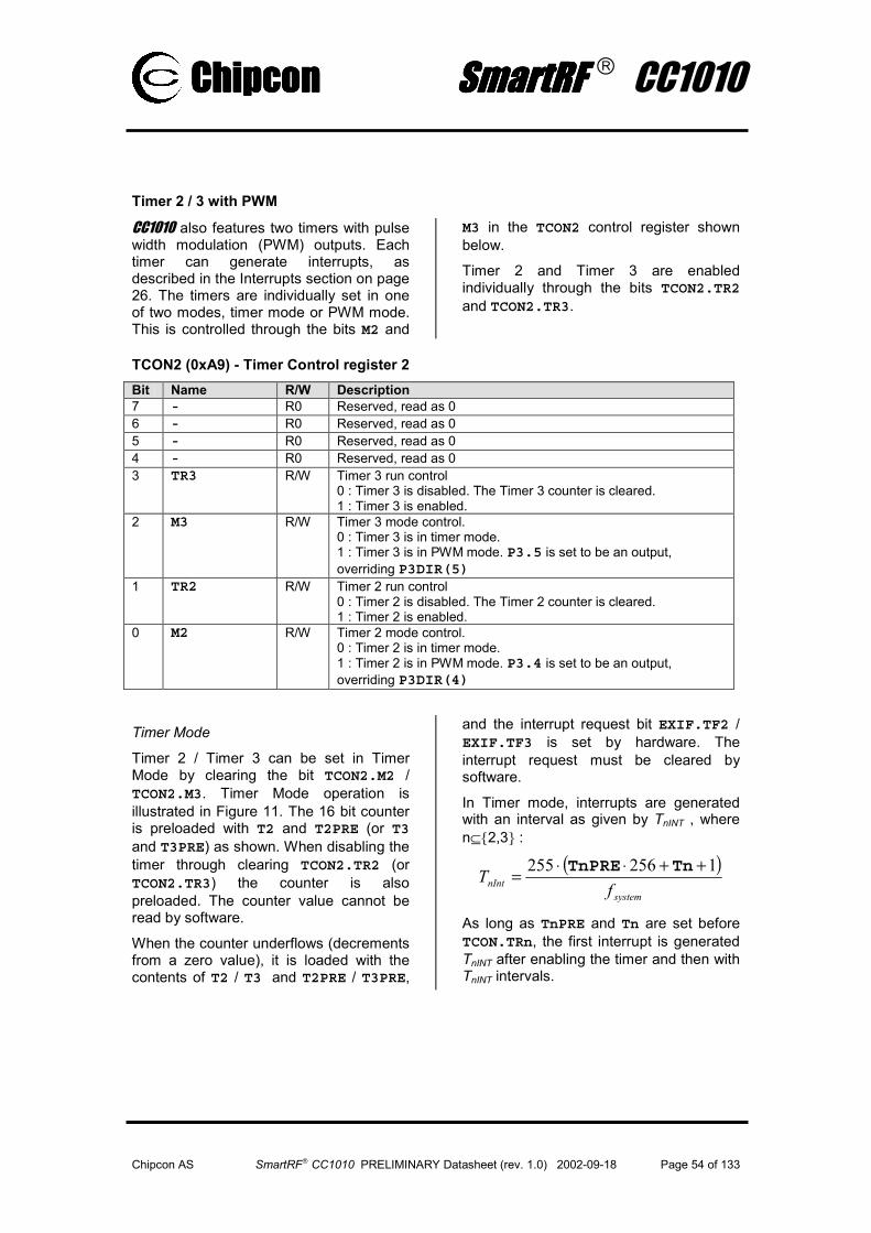
ChipconChipconChipconChipcon SmartRF SmartRF SmartRF SmartRF CC1010
Chipcon AS SmartRF CC1010 PRELIMINARY Datasheet (rev. 1.0) 2002-09-18 Page 54 of 133
Timer 2 / 3 with PWM
CC1010 also features two timers with pulse width modulation (PWM) outputs. Each timer can generate interrupts, as described in the Interrupts section on page 26. The timers are individually set in one of two modes, timer mode or PWM mode. This is controlled through the bits M2 and
M3 in the TCON2 control register shown below.
Timer 2 and Timer 3 are enabled individually through the bits TCON2.TR2 and TCON2.TR3.
TCON2 (0xA9) - Timer Control register 2 Bit Name R/W Description 7 - R0 Reserved, read as 0 6 - R0 Reserved, read as 0 5 - R0 Reserved, read as 0 4 - R0 Reserved, read as 0 3 TR3 R/W Timer 3 run control
0 : Timer 3 is disabled. The Timer 3 counter is cleared. 1 : Timer 3 is enabled.
2 M3 R/W Timer 3 mode control. 0 : Timer 3 is in timer mode. 1 : Timer 3 is in PWM mode. P3.5 is set to be an output, overriding P3DIR(5)
1 TR2 R/W Timer 2 run control 0 : Timer 2 is disabled. The Timer 2 counter is cleared. 1 : Timer 2 is enabled.
0 M2 R/W Timer 2 mode control. 0 : Timer 2 is in timer mode. 1 : Timer 2 is in PWM mode. P3.4 is set to be an output, overriding P3DIR(4)
Timer Mode
Timer 2 / Timer 3 can be set in Timer Mode by clearing the bit TCON2.M2 / TCON2.M3. Timer Mode operation is illustrated in Figure 11. The 16 bit counter is preloaded with T2 and T2PRE (or T3 and T3PRE) as shown. When disabling the timer through clearing TCON2.TR2 (or TCON2.TR3) the counter is also preloaded. The counter value cannot be read by software.
When the counter underflows (decrements from a zero value), it is loaded with the contents of T2 / T3 and T2PRE / T3PRE,
and the interrupt request bit EXIF.TF2 / EXIF.TF3 is set by hardware. The interrupt request must be cleared by software.
In Timer mode, interrupts are generated with an interval as given by TnINT , where n⊆2,3 :
( )system
nInt fT 1256255 ++⋅⋅= TnTnPRE
As long as TnPRE and Tn are set before TCON.TRn, the first interrupt is generated TnINT after enabling the timer and then with TnINT intervals.
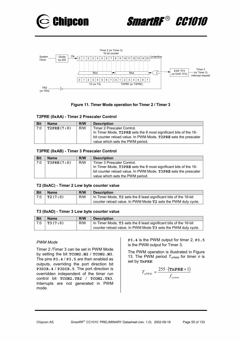
ChipconChipconChipconChipcon SmartRF SmartRF SmartRF SmartRF CC1010
Chipcon AS SmartRF CC1010 PRELIMINARY Datasheet (rev. 1.0) 2002-09-18 Page 55 of 133
Figure 11. Timer Mode operation for Timer 2 / Timer 3
T2PRE (0xAA) - Timer 2 Prescaler Control Bit Name R/W Description 7:0 T2PRE(7:0) R/W Timer 2 Prescaler Control.
In Timer Mode, T2PRE sets the 8 most significant bits of the 16-bit counter reload value. In PWM Mode, T2PRE sets the prescaler value which sets the PWM period.
T3PRE (0xAB) - Timer 3 Prescaler Control Bit Name R/W Description 7:0 T3PRE(7:0) R/W Timer 3 Prescaler Control.
In Timer Mode, T3PRE sets the 8 most significant bits of the 16-bit counter reload value. In PWM Mode, T3PRE sets the prescaler value which sets the PWM period.
T2 (0xAC) - Timer 2 Low byte counter value Bit Name R/W Description 7:0 T2(7:0) R/W In Timer Mode, T2 sets the 8 least significant bits of the 16-bit
counter reload value. In PWM Mode T2 sets the PWM duty cycle.
T3 (0xAD) - Timer 3 Low byte counter value Bit Name R/W Description 7:0 T3(7:0) R/W In Timer Mode, T3 sets the 8 least significant bits of the 16-bit
counter reload value. In PWM Mode T3 sets the PWM duty cycle.
PWM Mode
Timer 2 /Timer 3 can be set in PWM Mode by setting the bit TCON2.M2 / TCON2.M3. The pins P3.4 / P3.5 are then enabled as outputs, overriding the port direction bit P3DIR.4 / P3DIR.5. The port direction is overridden independent of the timer run control bit TCON2.TR2 / TCON2.TR3. Interrupts are not generated in PWM mode.
P3.4 is the PWM output for timer 2, P3.5 is the PWM output for Timer 3.
The PWM operation is illustrated in Figure 13. The PWM period TnPWM for timer n is set by TnPRE:
( )system
nPWM fT 1255 +⋅= TnPRE
Divideby 255
Timer 2 (or Timer 3)16 bit counter
EXIF.TF2(or EXIF.TF3)
Timer 2(or Timer 3)
interrupt request
Clk
Mux Mux
0 1 2 3 4 5 6 7 8 9 10 11 12 13 14 15
0 1 2 3 4 5 6 7 0 1 2 3 4 5 6 7T2 (or T3) T2PRE (or T3PRE)
Underflow
TR2(or TR3)
SystemClock

ChipconChipconChipconChipcon SmartRF SmartRF SmartRF SmartRF CC1010
Chipcon AS SmartRF CC1010 PRELIMINARY Datasheet (rev. 1.0) 2002-09-18 Page 56 of 133
The PWM “high” state duration TnhPWM for timer n is set by Tn:
systemnhPWM fT )1( +⋅= TnPRETn
This means that in PWM mode, setting Tn to 0 produces a constant low output and setting Tn to 255 produces a constant high output. The timing of the PWM outputs is illustrated in Figure 12.
PWMnOutput
TnPWM TnPWM
TnhPWM TnhPWM
Figure 12. PWM Timing illustration
System Clk Divide byTnPRE + 1
8 bit counter(counts 0-254)
A>B?PWM output
TnPWM
A
B
Timer 2 or Timer 3
Figure 13. PWM operation for Timer 2 / Timer 3

ChipconChipconChipconChipcon SmartRF SmartRF SmartRF SmartRF CC1010
Chipcon AS SmartRF CC1010 PRELIMINARY Datasheet (rev. 1.0) 2002-09-18 Page 57 of 133
Power On Reset (Brown-Out Detection) The Power On Reset functionality detects power-on and brown-out situations, and includes glitch immunity and hysteresis for noise and transient stability.
The power on reset functionality is disabled using the dedicated POR_E pin. Grounding POR_E will disable the internal
power on reset. An external power-on-reset module should then be connected to the external RESET_N pin.
The Power On Reset and Brown-Out Detection voltage levels are specified in the Electrical Specifications section at page 7.

ChipconChipconChipconChipcon SmartRF SmartRF SmartRF SmartRF CC1010
Chipcon AS SmartRF CC1010 PRELIMINARY Datasheet (rev. 1.0) 2002-09-18 Page 58 of 133
Watchdog Timer
CC1010 includes an 8 bit watchdog timer which is clocked by the system clock. The clock is divided by a number in the range from 2048 to 16384, controllable through WDT.WDTPRE(1:0). The divided clock
controls an 8 bit timer, which generates system reset upon overflow. A block diagram for the Watchdog Timer is shown in Figure 14.
WDT (0xD2) - Watchdog Timer Control Register Bit Name R/W Description 7 - R0 Reserved, read as 0 6 - R0 Reserved, read as 0 5 - R0 Reserved, read as 0 4 WDTSE R/W Watchdog Timer Stop Enable, used to disable the watchdog timer 3 WDTEN R/W Watchdog Timer Enable / Disable
0 : The watchdog timer is disabled 1 : The watchdog timer is enabled The watchdog timer is enabled after reset. To disable the watchdog timer, WDTSE must be used as described in this section.
2 WDTCLR R0/W Watchdog timer clear signal. WDTCLR must periodically be set to prevent the watchdog timer from resetting the system. WDTCLR is cleared by hardware, and is thus always read 0. 0 : Normal watchdog operation 1 : Watchdog timer is cleared.
1:0 WDTPRE.1 R/W Watchdog timer prescaler control. WDTPRE(1:0) controls the division of the main crystal oscillator clock to generate the watchdog timer clock. 00 : fWDT = fXOSC / 2048 01 : fWDT = fXOSC / 4096 10 : fWDT = fXOSC / 8192 11 : fWDT = fXOSC / 16384
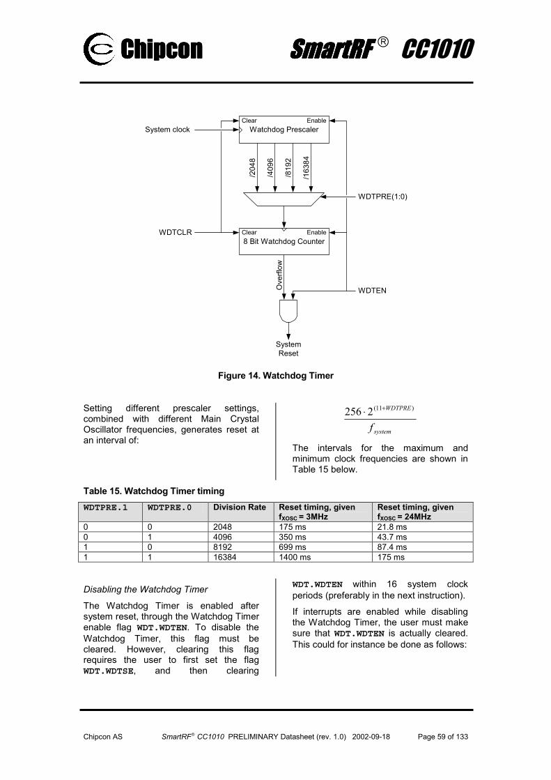
ChipconChipconChipconChipcon SmartRF SmartRF SmartRF SmartRF CC1010
Chipcon AS SmartRF CC1010 PRELIMINARY Datasheet (rev. 1.0) 2002-09-18 Page 59 of 133
System clock Watchdog Prescaler
/204
8
/409
6
/819
2
/163
84
WDTPRE(1:0)
8 Bit Watchdog Counter
Ove
rflow
WDTEN
SystemReset
Clear
Clear Enable
Enable
WDTCLR
Figure 14. Watchdog Timer
Setting different prescaler settings, combined with different Main Crystal Oscillator frequencies, generates reset at an interval of:
system
WDTPRE
f
)11(2256 +⋅
The intervals for the maximum and minimum clock frequencies are shown in Table 15 below.
Table 15. Watchdog Timer timing WDTPRE.1 WDTPRE.0 Division Rate Reset timing, given
fXOSC = 3MHz Reset timing, given fXOSC = 24MHz
0 0 2048 175 ms 21.8 ms 0 1 4096 350 ms 43.7 ms 1 0 8192 699 ms 87.4 ms 1 1 16384 1400 ms 175 ms
Disabling the Watchdog Timer
The Watchdog Timer is enabled after system reset, through the Watchdog Timer enable flag WDT.WDTEN. To disable the Watchdog Timer, this flag must be cleared. However, clearing this flag requires the user to first set the flag WDT.WDTSE, and then clearing
WDT.WDTEN within 16 system clock periods (preferably in the next instruction).
If interrupts are enabled while disabling the Watchdog Timer, the user must make sure that WDT.WDTEN is actually cleared. This could for instance be done as follows:

ChipconChipconChipconChipcon SmartRF SmartRF SmartRF SmartRF CC1010
Chipcon AS SmartRF CC1010 PRELIMINARY Datasheet (rev. 1.0) 2002-09-18 Page 60 of 133
while (WDT & 0x08) WDT |= 0x10; // Set WDTSEWDT &= ~0x08; // Clear WDTEN
Enabling the Watchdog Timer
Enabling the Watchdog Timer is simply done by setting WDT.WDTEN. It does not require using the WDT.WDTSE control bit.

ChipconChipconChipconChipcon SmartRF SmartRF SmartRF SmartRF CC1010
Chipcon AS SmartRF CC1010 PRELIMINARY Datasheet (rev. 1.0) 2002-09-18 Page 61 of 133
Realtime Clock The realtime clock can generate interrupts with intervals ranging from 1 to 127 seconds. It is connected to the 32.768 kHz crystal oscillator, which is disabled after reset. It must be enabled as described in the Power section on page 31. An external 32.768 kHz clock signal can also be applied, as described.
The interrupt interval is programmed in the range from 1 through 127 seconds by setting RTCON.RT(6:0). The timer is
enabled by setting RTCON.RTEN. The first interrupt will be generated RT seconds after RTEN is set.
The realtime clock interrupt must be enabled as described in the Interrupts section on page 26.
The RTC oscillator circuit is shown in Figure 15. The loading capacitors values can be calculated as described for the main crystal oscillator at page 30.
RTCON (0xED) - Realtime Clock Control Register Bit Name R/W Description 7 RTEN R/W Realtime Clock Enable / Disable
0 : Realtime Clock is disabled 1 : Realtime Clock is enabled
6:0 RT(6:0) R/W Realtime Clock interrupt interval control. RT(6:0) gives the desired interrupt interval in seconds. RT(6:0) must be between 1 and 127.
C13C12
XTAL32.768 kHzXTAL32.768 kHz
XOSC32_Q1 XOSC32_Q2
Figure 15. RTC oscillator circuit
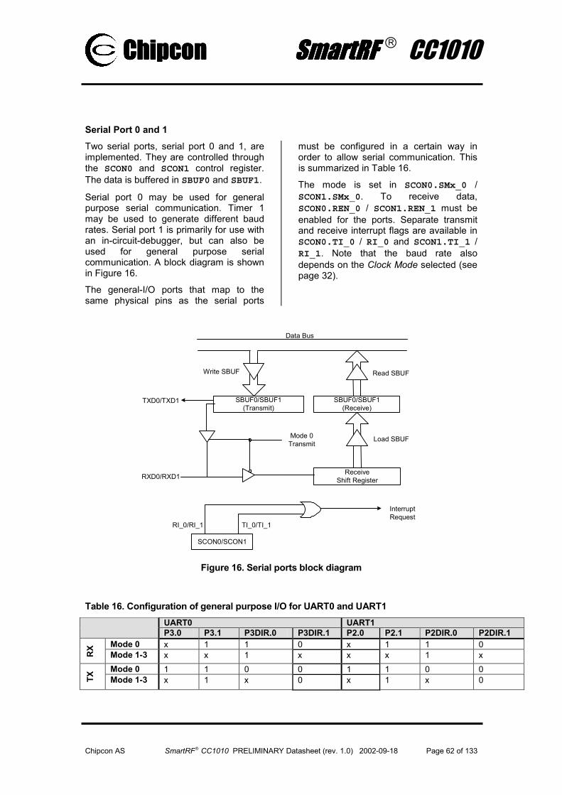
ChipconChipconChipconChipcon SmartRF SmartRF SmartRF SmartRF CC1010
Chipcon AS SmartRF CC1010 PRELIMINARY Datasheet (rev. 1.0) 2002-09-18 Page 62 of 133
Serial Port 0 and 1Two serial ports, serial port 0 and 1, are implemented. They are controlled through the SCON0 and SCON1 control register. The data is buffered in SBUF0 and SBUF1.
Serial port 0 may be used for general purpose serial communication. Timer 1 may be used to generate different baud rates. Serial port 1 is primarily for use with an in-circuit-debugger, but can also be used for general purpose serial communication. A block diagram is shown in Figure 16.
The general-I/O ports that map to the same physical pins as the serial ports
must be configured in a certain way in order to allow serial communication. This is summarized in Table 16.
The mode is set in SCON0.SMx_0 / SCON1.SMx_0. To receive data, SCON0.REN_0 / SCON1.REN_1 must be enabled for the ports. Separate transmit and receive interrupt flags are available in SCON0.TI_0 / RI_0 and SCON1.TI_1 / RI_1. Note that the baud rate also depends on the Clock Mode selected (see page 32).
SCON0/SCON1
ReceiveShift Register
SBUF0/SBUF1(Receive)
SBUF0/SBUF1(Transmit)
InterruptRequest
RI_0/RI_1 TI_0/TI_1
Read SBUFWrite SBUF
TXD0/TXD1
Load SBUFMode 0Transmit
RXD0/RXD1
Data Bus
Figure 16. Serial ports block diagram
Table 16. Configuration of general purpose I/O for UART0 and UART1 UART0 UART1 P3.0 P3.1 P3DIR.0 P3DIR.1 P2.0 P2.1 P2DIR.0 P2DIR.1
Mode 0 x 1 1 0 x 1 1 0
RX
Mode 1-3 x x 1 x x x 1 x Mode 0 1 1 0 0 1 1 0 0
TX
Mode 1-3 x 1 x 0 x 1 x 0

ChipconChipconChipconChipcon SmartRF SmartRF SmartRF SmartRF CC1010
Chipcon AS SmartRF CC1010 PRELIMINARY Datasheet (rev. 1.0) 2002-09-18 Page 63 of 133
SBUF0 (0x99) - Serial Port 0, data buffer Bit Name R/W Description 7:0 SBUF0(7:0) R/W Serial Port 0, data buffer.
SBUF1 (0xC1) – Serial Port 1, data buffer Bit Name R/W Description 7:0 SBUF1(7:0) R/W Serial Port 1, data buffer
SCON0 (0x98) - Serial Port 0 Control Register Bit Name R/W Description 7 SM0_0 R/W
6 SM1_0 R/W
Serial Port 0 mode bits, decoded as: SM0_0 SM1_0 Mode 0 0 0 (Synchronous half duplex) 0 1 1 (Asynchronous full duplex, start + stop bit) 1 0 2 (Asynchronous full duplex, start + stop bit, 9th
data bit) 1 1 3 (Asynchronous full duplex, start + stop bit, 9th
data bit) 5 SM2_0 R/W Multiprocessor communication enable. In modes 2 and 3 SM2_0
= 1 enables the multiprocessor communication feature: In mode 2 or 3 RI_0 will not be activated if the received 9th bit is 0. If SM2_0 = 1 in mode 1, RI_0 will only be activated if a valid stop bit is received. In mode 0 SM2_0 establishes the baud rate: when SM2_0 = 0 the baud rate is clk / 12; when SM2_0 = 1 the baud rate is clk / 4.
4 REN_0 R/W Receive enable. When REN_0 = 1 reception is enabled.
3 TB8_0 R/W Defines the state of the 9th data bit transmitted in modes 2 and 3.
2 RB8_0 R/W In modes 2 and 3 RB8_0 indicates the state of the 9th bit received. In mode 1 RB8_0 indicates the state of the received stop bit. In mode 0 RB8_0 is not used.
1 TI_0 R/W Transmit interrupt flag. Indicates that the transmit data word has been shifted out. In mode 0 TI_0 is set at the end of the 8th data bit. In all other modes TI_0 is set when the stop bit is placed on the TXD0 pin. TI_0 must be cleared by the software.
0 RI_0 R/W Receive interrupt flag. Indicates that a serial data word has been received. In mode 0 RI_0 is set at the end of the 8th data bit. In mode 1 RI_0 is set after the last sample of the incoming stop bit, subject to the state of SM2_0. In modes 2 and 3 RI_0 is set at the end of the last sample of RB8_0. RI_0 must be cleared by the software.

ChipconChipconChipconChipcon SmartRF SmartRF SmartRF SmartRF CC1010
Chipcon AS SmartRF CC1010 PRELIMINARY Datasheet (rev. 1.0) 2002-09-18 Page 64 of 133
SCON1 (0xC0) - Serial Port 1 Control Register Bit Name R/W Description 7 SM0_1 R/W
6 SM1_1 R/W
Serial Port 1 mode bits, decoded as: SM0_1 SM1_1 Mode 0 0 0 (Synchronous half duplex) 0 1 1 (Asynchronous full duplex, start + stop bit) 1 0 2 (Asynchronous full duplex, start + stop bit, 9th
data bit) 1 1 3 (Asynchronous full duplex, start + stop bit, 9th
data bit) 5 SM2_1 R/W Multiprocessor communication enable. In modes 2 and 3 SM2_1
= 1 enables the multiprocessor communication feature: In mode 2 or 3 RI_1 will not be activated if the received 9th bit is 0. If SM2_1 = 1 in mode 1 RI_1 will only be activated if a valid stop bit is received. In mode 0 SM2_1 establishes the baud rate: when SM2_1 = 0 the baud rate is clk / 12; when SM2_1= 1 the baud rate is clk / 4.
4 REN_1 R/W Receive enable. When REN_1 = 1 reception is enabled.
3 TB8_1 R/W Defines the state of the 9th data bit transmitted in modes 2 and 3.
2 RB8_1 R/W In modes 2 and 3 RB8_1 indicates the state of the 9th bit received. In mode 1 RB8_1 indicates the state of the received stop bit. In mode 0 RB8_1 is not used.
1 TI_1 R/W Transmit interrupt flag. Indicates that the transmit data word has been shifted out. In mode 0 TI_1 is set at the end of the 8th data bit. In all other modes TI_1 is set when the stop bit is placed on the TXD1 pin. TI_1 must be cleared by the software.
0 RI_1 R/W RI_1 – Receive interrupt flag. Indicates that a serial data word has been received. In mode 0 RI_1 is set at the end of the 8th data bit. In mode 1 RI_1 is set after the last sample of the incoming stop bit, subject to the state of SM2_1. In modes 2 and 3 RI_1 is set at the end of the last sample of RB8_1. RI_1 must be cleared by the software.
MODE 0
Serial mode 0 provides synchronous, half-duplex serial communication. For serial port 0, pin RXD0 (P3.0) is used for data input and output while TXD0 (P3.1) provides the bit clock for both transmit and receive. For serial port 1 the corresponding pins are RXD1 (P2.0) and TXD1 (P2.1).
The serial mode 0 baud rate is set by SCON0.SM2_0 / SCON1.SM2_1. If this bit is cleared, the baud rate is the system clock divided by 4. If the bit is set, the system clock is divided by 12.
Data transmission begins when an instruction writes to the SBUF0 (or SBUF1) register. The serial port shifts the data byte out, LSB first, at the selected baud rate.
Data recepion starts when SCON0.REN_0 / SCON1.REN_1 is set and the receive interrupt flag SCON0.RI_0 / SCON1.RI_1 is cleared. The bit clock is activated and the UART shifts data in on each rising edge of the bit clock, until 8 bits have been received. Immediately after the 8th bit is shifted in, the receive interrupt flag is set and reception stops until the software clears the flag.

ChipconChipconChipconChipcon SmartRF SmartRF SmartRF SmartRF CC1010
Chipcon AS SmartRF CC1010 PRELIMINARY Datasheet (rev. 1.0) 2002-09-18 Page 65 of 133
The clock output is high when the serial port is idle. In reception, data is shifted in on the rising edge of the clock. In transmission, each new bit is set on the falling edge of the clock.
MODE1
Mode 1 provides standard asynchronous full duplex communication, using a total of 10 bits: 1 start bit, 8 data bits and 1 stop bit. For receive operations, the stop bit is stored in SCON0.RB8_0 (or SCON1.RB8_1). Data bits are received and transmitted with their LSB first.
The baud rate for mode 1 is a function of timer 1 overflow. Each time the timer increments from its maximum count (0xFF), a clock pulse is sent to the baud rate circuit, to be further divided by 16 or 32 as set by PCON.SMOD0 / EICON.SMOD1 to give the baudrate:
overflowTimerRateBaud 132
2 ⋅=SMODx
As can be seen from the equation above, if both serial ports are in use simultaneously, the baud rate is equal or different by a factor 2.
It is common to use Timer 1 in Mode 2 (8-bit counter with auto-reload) for baud rate generation, although any timer mode can be used. The Timer 1 reload value is stored in the TH1 register, which makes the complete baudrate using mode 2:
)256()812(322
TH1T1M
SMODx
−⋅⋅−⋅= systemf
RateBaud
T1M in the above equation is in register CKCON (see page 51), and controls the initial division in Timer 1 between 4 and 12.
Some example baudrates and reload values are shown in Table 17. The setting for other baud rates and oscillator frequencies can easily be found using the above equation.
Table 17. Baudrate examples (SMODx=1)
T1M/TH1 Baudrate Fxosc = 11.0592 MHz
Fxosc = 14.7456 MHz
57.6 0/255 1/252 19.2 0/253 0/252 9.6 0/250 0/248 4.8 0/244 0/240 2.4 0/232 0/224 1.2 0/208 0/192
To transmit data in mode 1, write data to SBUF0 / SBUF1. Transmission is then performed on TXD0 / TXD1 in the following order: start bit, 8 data bits (LSB first) and then the stop bit.
Reception begins on the falling edge of a start bit received on RXD0 / RXD1, if reception is enabled in SCON0.REN_0 / SCON1.REN_1. The data input is sampled 16 times per baud for any baud rate. Each bit decision is performed as a majority decision between 3 successive samples in the middle of each baud. If the majority decision is not equal to zero for the start bit, the serial port will stop reception and wait for a new start bit.
When the majority decision is made for the stop-bit, the following conditions must be met:
• RI_0 / RI_1 is 0
• If SM2_0 / SM2_1 is set, the state of the stop bit must be one
If these conditions are met, the received data is buffered in SBUF0 / SBUF1, the received stop bit is stored in RB8_0 / RB8_1) and the receive interrupt flag is set. If not, the received data is lost and RB8_0 / RB8_1 and the receive interrupt flag remains unchanged.
MODE2
Mode 2 provides asynchronous full-duplex communication using a total of 11 bits: 1 start bit, 8 data bits, a programmable 9th bit and 1 stop bit. The data bits are transmitted and received LSB first.

ChipconChipconChipconChipcon SmartRF SmartRF SmartRF SmartRF CC1010
Chipcon AS SmartRF CC1010 PRELIMINARY Datasheet (rev. 1.0) 2002-09-18 Page 66 of 133
The mode 2 baud rate is either fsystem/32 or fsystem/64, set by PCON.SMOD0 (or EICON.SMOD1). The baud rate is then:
systemfRateBaud ⋅=64
2SMODx
To transmit data in mode 1, write data to SBUF0 / SBUF1. Transmission is then performed on pin TXD0 / TXD1 in the following order: start bit, 8 data bits (LSB first), 9th bit (from TB8_0 / TB8_1) and then the stop bit. The transmit interrupt flag TI_0 / TI_1 is set when the stop bit is placed on the transmit pin.
Reception must be enabled by setting REN_0 / REN_1. It is then initiated by the falling edge of a start bit received on RXD0 / RXD1. The input pin is sampled 16 times per baud. Majority decision is made, as with mode 1. When the majority decision is made for the stop-bit, the following conditions must be met:
• RI_0 / RI_1 is 0
• If SM2_0 / SM2_1 is set, the 9th bit and the stop bit must be one.
If these conditions are met, the received data is buffered in SBUF0 / SBUF1, the received stop bit is stored in RB8_0 / RB8_1 and the receive interrupt flag RI_0 / RI_1 is set. If not, the received data is
lost and RB8 and the receive interrupt flag remains unchanged.
MODE 3
Mode 3 provides asynchronous, full-duplex communication, using a total of 11 bits (as with mode 2): 1 start bit, 8 data bits, a programmable 9th bit and 1 stop bit. The data bits are transmitted and received LSB first.
Transmission and reception in mode 3 is identical to mode 2, except for the baud rate generation, which is identical to mode 1.
Multiprocessor Communications
The multiprocessor communication feature is enabled in mode2 and mode 3, when the SM2_0 / SM2_1 bit is set. The 9th bit received is then stored in RB8_0 / RB8_1 and the interrupt bit is only set if this bit is 1.
An address byte can then be transmitted, with the 9th bit set, to generate an interrupt on all slaves. The slave(s) with the correct address (decoded in software) may then clear SM2_0 / SM2_1 to receive the rest of the data, which is transmitted with the 9th bit low. All other slaves will then ignore the data received.

ChipconChipconChipconChipcon SmartRF SmartRF SmartRF SmartRF CC1010
Chipcon AS SmartRF CC1010 PRELIMINARY Datasheet (rev. 1.0) 2002-09-18 Page 67 of 133
SPI Master
The SPI master interface allows CC1010 to communicate with peripheral devices such as an external serial EEPROM interface. It has a programmable datarate up to 3 MHz, depending on the frequency of the crystal attached.
The SPI master interface is controlled using the SPCR register shown below.
Setting SPCR.SPE enables the SPI interface. Pins P0.0, P0.1 and P0.2 are then reconfigured as the serial clock output SCK, the serial data output pin MO and the serial data input pin MI. The direction bits set in P0DIR(0) and P0DIR(2) are then ignored, setting SCK
as an output and MI as an input. The direction bit P0DIR(1) still determines the direction of the master data output pin MO. This allows the SPI master to communicate with a bidirectional data line. P0DIR(1) should then be cleared when transmitting and set when receiving data, with MO and MI connected together externally. For normal full-duplex operation of the SPI master, P0DIR(1) must be cleared to set MO as an output.
Any other general purpose I/O-pin may be used for slave select signals to the peripheral modules.
SPCR (0xA1) - SPI Control Register Bit Name R/W Description 7 - R0 Reserved, read as 0 6 - R/W Reserved, write 0 5 SPE R/W0 SPI Enable.
0 : SPI interface is disabled 1 : SPI interface is enabled
4 DORD R/W Data Order 0 : Least significant bit (LSB) is transmitted / received first 1 : Most significant bit (MSB) is transmitted / received first
3 CPOL R/W Clock Polarity 0 : SCK has negative clock polarity 1 : SCK has positive clock polarity
2 CPHA R/W Clock Phase
0 : Data is output on DO when SCK goes from CPOL to CPOL
and is sampled from DI when SCK goes from CPOL to CPOL
1 : Data is output on DO when SCK goes from CPOL to CPOL
and is sampled from DI when SCK goes from CPOL to CPOL
1:0 SPR(1:0) R/W SPI Data Rate. SPR(1:0) 00 : SCK clock frequency = fXOSC / 8 01 : SCK clock frequency = fXOSC / 16 10 : SCK clock frequency = fXOSC / 32 11 : SCK clock frequency = fXOSC / 64
SPDR (0xA2) - SPI Data Register Bit Name R/W Description 7:0 SPDR(7:0) R/W SPI Data Register
Writing to SPDR when SPCR.SPE is set will initiate a data transmission. Reading SPDR will read the data input buffer, which is only updated after each completed transmission.

ChipconChipconChipconChipcon SmartRF SmartRF SmartRF SmartRF CC1010
Chipcon AS SmartRF CC1010 PRELIMINARY Datasheet (rev. 1.0) 2002-09-18 Page 68 of 133
SPSR (0xA3) - SPI Status Register Bit Name R/W Description 7:2 - R0 Reserved, read as 0 1 SPA R SPI Active status bit
0 : The SPI interface is currently not transmitting data 1 : The SPI interface is currently transmitting data
0 WCOL R Write collision flag. This flag is updated by hardware when SPDR is written. 0 : The previous write to SPDR did not generate a data collision. 1 : The previous write to SPDR generated a data collision
Writing data to SPDR when SPCR.SPE is set will initiate a data transmission. 8 bits are transmitted and received with the data order, clock polarity, clock phase and data rate as set by SPCR.DORD, SPCR.CPOL, SPCR.CPHA and SPCR.SPR.
Reading data from SPDR will read the input buffer, which is only updated after each complete transmission. This means that a new byte can be written to SPDR before reading the newly received byte in order to maximise the data rate.
If data is written to SPDR while a transmission is in progress, this is regarded as a collision. After each new byte written to SPDR, the write collision flag SPSR.WCOL is updated. If a collision occurs, the data written to SPDR is ignored
and the data must be written to SPDR again to be sent.
It is also possible to check the SPI status bit, SPSR.SPA, before writing to SPDR to avoid collisions. This bit is set only when data is being transmitted.
SPI timing, data order, clock polarity and clock phase are shown in Figure 17.

ChipconChipconChipconChipcon SmartRF SmartRF SmartRF SmartRF CC1010
Chipcon AS SmartRF CC1010 PRELIMINARY Datasheet (rev. 1.0) 2002-09-18 Page 69 of 133
SCK(CPOL=0, CPHA=0)
SCK(CPOL=0, CPHA=1)
SCK(CPOL=1, CPHA=0)
SCK(CPOL=1, CPHA=1)
MO / MIDORD=0
0 1 2 3 4 5 6 7
MO / MIDORD=1
7 6 5 4 3 2 1 0
SPSR.SPA
SPSR.WCOL is set if SPDR is written here
SPDR read by 8051 Data received during last byte transmission New data
SPDR is written by 8051 here,while SPCR.SPE is active
Figure 17. SPI Data Flow
ChipconChipconChipconChipcon SmartRF SmartRF SmartRF SmartRF CC1010
Chipcon AS SmartRF CC1010 PRELIMINARY Datasheet (rev. 1.0) 2002-09-18 Page 70 of 133
DES Encryption / DecryptionDES encryption / decryption is supported by hardware in CC1010. Blocks of data ranging from 1 to 256 bytes can be encrypted / decrypted in one operation by the DES module. Multiple encryption / decryption operations can also be used on larger data blocks.
Encryption is the process of encoding an information bit stream to secure the data content. The DES algorithm is a common, simple and well-established encryption routine. An encryption key of 56 bits is used to encrypt the message. The receiver must use the exact same key to decrypt the message, otherwise garbage will be produced. The encryption and decryption operations in the DES algorithm are reverse operations with the same computational requirements. The operations produce the same number of output bytes as input bytes. The strength of an encryption algorithm is determined by the number of bits in the key, the more the better. The DES algorithm offers a low to medium level of security. If higher levels of security are required, a triple DES algorithm can be used. Triple DES can be achieved by running the DES algorithm three times sequentially using three different 56-bit encryption keys. The keys must be used in reverse order when decrypting.
The DES algorithm works internally on entities of 8 bytes. The Output Feedback Mode (OFB) and Cipher Feedback Mode (CFB) are DES modes of operation that permit data lengths that are not a multiple of eight bytes. The operation mode is selected through the CRPCON.CRPMD control bit. The same DES mode of operation must be used both for encryption and decryption to yield correct results. CFB is recommended as it is more secure than OFB.
CRPCON.ENCDEC should be cleared when encrypting data and set when decrypting data.
56 bit DES keys are stored in external RAM, as shown in Table 18. The location
is given by the register CRPKEY, containing the 8 most significant address bits. New keys are loaded only at the beginning of an encryption / decryption if CRPCON.LOADKEYS is set. If not, the same keys as used in the previous run will be used again.
The DES keys do not contain parity bits. If DES keys with parity bits are given, the parity bits must be removed before performing encryption / decryption. The keys are therefore stored as 7 successive bytes in RAM.
After running the DES, a output block O of length CRPCNT bytes is generated by encrypting / decrypting the input block I of same length as O using key K1 as follows:
O=EK1(I) (encryption)
O=DK1(I) (decryption)
The following is an example on how to use the single DES algorithm hardware in CC1010. First the 56-bit encryption key must be stored in the external RAM. Then the CRPKEY register must be written to point to the start of the encryption key. Note that the encryption key must start on a RAM address location divisible by 8. Then the data bit stream to encrypt must be stored in the external RAM. The data bit stream must consist of at least 1 byte up to a maximum of 256 bytes, and it must also start on a RAM address location divisible by 8. The CRPDAT register must be written to point to the start of the data bit stream, and CRPCNT must be written to give the number of bytes to be encrypted. Then the CRPINI0, CRPINI1,CRPINI2, CRPINI3, CRPINI4,CRPINI5, CRPINI6, CRPINI7 registers must be written to contain the DES initialisation vector used in the OFB and CFB modes of operation. For simplicity it can be set to all zeros. Note that the initialisation vector must be the same for both encryption and decryption to yield correct results. To initiate the encryption the CRPCON register must be written. The bits in this register select

ChipconChipconChipconChipcon SmartRF SmartRF SmartRF SmartRF CC1010
Chipcon AS SmartRF CC1010 PRELIMINARY Datasheet (rev. 1.0) 2002-09-18 Page 71 of 133
encryption/decryption, feedback mode, and DES interrupt enable. When the encryption has been completed, CRPCON.CRPEN goes low and the DES interrupt flag is set. The external RAM will
now contain the encrypted data bit stream in the same location as the input data bytes were originally put. To perform the reverse operation, write CRPCON again with the CRPCON.ENCDEC bit set.
Table 18. DES key location in RAM Key First RAM Location Last RAM Location K1 8 ⋅ CRPKEY 8 ⋅ CRPKEY+6
Encryption / decryption is done in-place, i.e. each byte of data read from external RAM for encryption / decryption will be written back to the same location after encryption / decryption as described above. The input and output blocks must start on an address which is a multiple of eight. CRPDAT then gives the 8 most significant address bits to the first data byte.
The encryption / decryption initialization vector should be written to registers CRPINI0 to CRPINI7. These registers must be written prior to encrypting / decrypting a new block of data, as they are modified by hardware. They should be left unchanged between multiple encryption / decryption operations for DES blocks larger than 256 bytes. A zero value initialisation vector can be used, or additional security can be effected by using the initialisation vector as an additional key.
Encryption / decryption is started when CRPCON.CRPEN is set. When the encryption / decryption is completed, CRPCON.CRPEN is cleared by hardware and the interrupt flag CRPCON.CRPIF is set. If CRPCON.CRPIE is set, the interrupt flag EXIF.ADIF is also set, which will generate an interrupt if EIE.ADIE is set. (See the Interrupts section on page 26 for details on interrupts.)
The duration of a DES encryption / decryption operation is shown in Table 19. Accessing external RAM from the 8051 while encrypting / decrypting may delay the operation slightly since the access is multiplexed.
DES keys stored in Flash memory will be protected by the Flash memory protection. For the security of the Flash protection, please refer to the disclaimer at the end of this document.
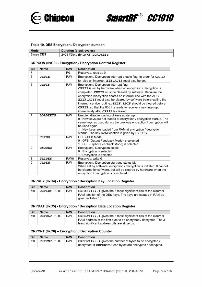
ChipconChipconChipconChipcon SmartRF SmartRF SmartRF SmartRF CC1010
Chipcon AS SmartRF CC1010 PRELIMINARY Datasheet (rev. 1.0) 2002-09-18 Page 72 of 133
Table 19. DES Encryption / Decryption duration Mode Duration (clock cycles) Single DES 2+25⋅#Data Bytes +21⋅LOADKEYS
CRPCON (0xC3) - Encryption / Decryption Control Register Bit Name R/W Description 7 - R0 Reserved, read as 0 6 CRPIE R/W Encryption / Decryption interrupt enable flag. In order for CRPIF
to raise an interrupt, EIE.ADIE must also be set. 5 CRPIF R/W Encryption / Decryption interrupt flag.
CRPIF is set by hardware when an encryption / decryption is completed. CRPIF must be cleared by software. Because the encryption /decryption shares an interrupt line with the ADC, EXIF.ADIF must also be cleared by software before exiting the interrupt service routine.. EXIF.ADIF should be cleared before CRPIF, so that the 8051 is ready to receive a new interrupt immediately after CRPIF is cleared.
4 LOADKEYS R/W Enable / disable loading of keys at startup. 0 : New keys are not loaded at encryption / decryption startup. The same keys as used during the previous encryption / decryption will be used again. 1 : New keys are loaded from RAM at encryption / decryption startup. The key RAM location is given by CRPKEY.
3 CRPMD R/W OFB / CFB Mode 0 : OFB (Output Feedback Mode) is selected 1 : CFB (Cipher Feedback Mode) is selected
2 ENCDEC R/W Encryption / Decryption select 0 : Encryption is selected 1 : Decryption is selected
1 TRIDES R/W0 Reserved, write 0 0 CRPEN R/W1 Encryption / Decryption start and status bit.
When set by software, encryption / decryption is initiated. It cannot be cleared by software, but will be cleared by hardware when the encryption / decryption is completed.
CRPKEY (0xC4) - Encryption / Decryption Key Location Register Bit Name R/W Description 7:0 CRPKEY(7:0) R/W CRPKEY(7:0) gives the 8 most significant bits of the external
RAM location of the DES keys. The keys are located in RAM as given in Table 18.
CRPDAT (0xC5) - Encryption / Decryption Data Location Register Bit Name R/W Description 7:0 CRPDAT(7:0) R/W CRPDAT(7:0) gives the 8 most significant bits of the external
RAM address of the first byte to be encrypted / decrypted. The 3 least significant address bits are all zeros.
CRPCNT (0xC6) – Encryption / Decryption Counter Bit Name R/W Description 7:0 CRPCNT(7:0) R/W CRPCNT(7:0) gives the number of bytes to be encrypted /
decrypted. If CRPCNT=0, 256 bytes are encrypted / decrypted.
ChipconChipconChipconChipcon SmartRF SmartRF SmartRF SmartRF CC1010
Chipcon AS SmartRF CC1010 PRELIMINARY Datasheet (rev. 1.0) 2002-09-18 Page 73 of 133
CRPINIn, n∈∈∈∈0..7 (0xB4-0xB7, 0xBC-0xBF) - DES Initialisation Vector Bit Name R/W Description 7:0 CRPINIn
(7:0)R/W The 8 registers CRPINIn, n ∈0..7, contains the 64 bit DES
initialisation vector. Bits 8⋅n-1 down to 8⋅n are located in register CRPINIn

ChipconChipconChipconChipcon SmartRF SmartRF SmartRF SmartRF CC1010
Chipcon AS SmartRF CC1010 PRELIMINARY Datasheet (rev. 1.0) 2002-09-18 Page 74 of 133
Random Bit Generation
CC1010 can generate real random bit sequences to be used as encryption keys, seed for a software pseudo random generator or other purposes. The data is generated from amplifying noise in the RF receiver path.
To enable random bit generation, set RANCON.RANEN and clear RFMAIN.RX_PD. Wait at least 1 ms before reading data from RANCON.RANBIT. The period between reads should be at least 10 µs for the data to be as random as possible.
For applications requiring guaranteed DC free data, software should process the generated data, for example by xor'ing two successive bits.
The random data generated has a relatively white spectrum, but tones have been observed when the random bit generator has been enabled for more than one second. If this is not sufficient for the application to generate the random bits required, the random bit generator should be disabled and enabled following the procedure described above before generating more data.
RANCON (0xC7) - Random Bit Generator Control Register Bit Name R/W Description 7:2 - R0 Reserved, read as 0 1 RANEN R/W Random Bit Generator Enable
0 : Random Bit Generator is disabled. 1 : Random Bit Generator is enabled. RFMAIN.RX_PD must also be cleared to generate random bits.
0 RANBIT R RANBIT returns one random bit, generated from the RF receiver path.

ChipconChipconChipconChipcon SmartRF SmartRF SmartRF SmartRF CC1010
Chipcon AS SmartRF CC1010 PRELIMINARY Datasheet (rev. 1.0) 2002-09-18 Page 75 of 133
ADC The on-chip 10 bit ADC is controlled by the registers ADCON and ADCON2.
Three analog pins can be sampled, controlled by ADCON.ADADR. This register is also used to select the AD1 pin as external reference (when using AD0).
The analog reference voltage is controlled by ADCON.ADCREF. ADCON.AD_PD should be set when the ADC is not is use to save power. A conversion can be started 5 µs after clearing the bit when using VDD or an external reference, or 100 µs afterwards when using the internal 1.25V reference.
The ADC can be operated in 4 modes controlled by ADCON.ADCM. Each ADC sample conversion takes 11 ADC clock cycles. In Clock Mode 1, when POWER.PMODE is set, the 32 kHz clock is applied directly to the ADC. In Clock Mode 0 the ADC clock input is derived from the main oscillator clock using the divider selected by ADCON2.ADCDIV. The register must be set so that the resulting ADC clock frequency is less than or equal to 250 kHz.
In single-conversion mode each conversion is initiated by setting the ADCON.ADCRUN control bit. The ADC interrupt flags EXIF.ADIF and ADCON2.ADCIF are set by hardware if the 8 MSB of the latest sampled value is greater than or equal to the threshold value stored in the ADTRH register. An interrupt service routine is then executed if the interrupt enable flags EIE.ADIE and ADCON2.ADCIE are set. To always get an interrupt upon completion of a conversion, ADTRH should be set to 0. The ADCON.ADCRUN control bit is cleared by hardware when the conversion is finished.
In the multi-conversion modes the ADC starts a new conversion every 11th ADC clock cycle. All multi-conversion modes can be stopped by clearing ADCON.ADCRUN, after which the ADC will abort its current conversion and then stop. In all modes an action is taken when the 8 MSB of the latest sample value is greater than or equal to the value written in ADTRH; these are:
Multi-conversion, continuous. When the threshold comparison holds true (value ≥ ADTRH⋅ 4) an interrupt is generated and the corresponding interrupt service routine is then executed if the interrupt enable flags EIE.ADIE and ADCON2.ADCIE are set. The ADC will continue its conversions regardless of the result of the threshold comparison. To always get an interrupt upon completion of a conversion, ADTRH should be set to 0.
Multi-conversion, stopping. When the threshold comparison holds true (value ≥ ADTRH⋅ 4) an interrupt is generated and the corresponding interrupt service routine is then executed if the interrupt enable flags EIE.ADIE and ADCON2.ADCIE are set. The ADC will stop when the threshold comparison holds true, clearing ADCON.ADCRUN.
Multi-conversion, reset-generating. When the threshold comparison holds true (value ≥ ADTRH⋅ 4) a system reset is generated. This mode can be used in conjunction with the 8051's stop mode and the 32 kHz oscillator to achieve very low power consumptions while monitoring a signal. The value stored in ADDATH and ADDATL are not affected by a reset, such that the sampled value can be read back after the reset has taken effect.

ChipconChipconChipconChipcon SmartRF SmartRF SmartRF SmartRF CC1010
Chipcon AS SmartRF CC1010 PRELIMINARY Datasheet (rev. 1.0) 2002-09-18 Page 76 of 133
ADCON (0x93) - ADC Control Register Bit Name R/W Description 7 AD_PD R/W ADC Power down bit.
0 : ADC is active 1 : ADC is in power down
6 - R0 Reserved, read as 0
5:4 ADCM(1:0) R/W ADC Mode: 00 : Single-conversion mode. (Interrupt when threshold condition holds true, stop after one conversion.) 01 : Multi-conversion mode, continuous. (Interrupt when threshold condition holds true, continue sampling.) 10 : Multi-conversion mode, stopping. (Interrupt when threshold condition holds true, stop sampling.) 11: Multi-conversion mode, reset-generating. (Generate reset when threshold condition holds true.)
3 ADCREF R/W Select the internal ADC Voltage Reference 0 : Voltage reference is VDD 1 : Voltage reference is 1.25 V, generated on chip.
2 ADCRUN R/W ADC run control. Setting this bit in software will start ADC operation in single- or multi-conversion mode. In single conversion mode this bit is cleared by hardware when the single conversion is done. Multi-conversion operation can be halted at the end of the current conversion by clearing this bit. (When ADCM=10 the hardware clears this bit when stopping.)
1:0 ADADR(1:0) R/W Select the analog input to the ADC 00 : Mux data from the AD0 pin 01 : Mux data from the AD1 pin 10 : Mux data from the AD2 (RSSI/IF) pin 11 : Mux data from the AD0 pin with AD1 as an external reference. ADCREF is ignored in this setting
ADDATL (0x94) - ADC Data Register, Low Byte Bit Name R/W Description 7:0 ADDAT(7:0) R 8 LSB of ADC data output
ADDATH (0x95) - ADC Data Register, High Bits Bit Name R/W Description 7:2 - R0 Reserved, read as 0 1:0 ADDAT(9:8) R 2 MSB of ADC data output, latched when ADDATL is read

ChipconChipconChipconChipcon SmartRF SmartRF SmartRF SmartRF CC1010
Chipcon AS SmartRF CC1010 PRELIMINARY Datasheet (rev. 1.0) 2002-09-18 Page 77 of 133
ADCON 2(0x96) - ADC Control Register 2 Bit Name R/W Description 7 ADCIE R/W ADC interrupt enable flag. In order for ADCIF to raise an interrupt,
EIE.ADIE must also be set. 6 ADCIF R/W ADC interrupt flag. ADCIF must be cleared by software. Because
the ADC shares an interrupt line with the DES module, EXIF.ADIF must also be cleared by software before exiting the interrupt service routine. EXIF.ADIF should be cleared first so that the 8051 is ready to receive a new interrupt immediately after ADCIF is cleared.
5:0 ADCDIV R/W ADC clock divider. Selects ADC clock divider in steps of 16. 000000: Divider is 16 000001: Divider is 32 … 111111: Divider is 1024
ADTRH (0x97) - ADC Threshold Register Bit Name R/W Description 7:0 ADTRH(7:0) R/W ADC comparator threshold value, used to generate ADC interrupt
or chip reset when the threshold is exceeded, as described.

ChipconChipconChipconChipcon SmartRF SmartRF SmartRF SmartRF CC1010
Chipcon AS SmartRF CC1010 PRELIMINARY Datasheet (rev. 1.0) 2002-09-18 Page 78 of 133
RF Transceiver
General description
The CC1010 UHF RF Transceiver is designed for very low power and low voltage applications. The transceiver circuit is mainly intended for the ISM (Industrial, Scientific and Medical) and SRD (Short Range Device) frequency bands at 315, 433, 868 and 915 MHz, but can easily be programmed for operation at other frequencies in the 300-1000 MHz range.
The main operating parameters of CC1010 can be programmed via Special Function Registers (SFRs), thus making CC1010 a very flexible and easy to use transceiver.
Very few external passive components are required for operation of the RF Transceiver.
The key parameters for the RF transceiver are listed in Table 4, page 7.
RF Transceiver Block Diagram
Figure 18. Simplified block diagram of the RF Transceiver
A simplified block diagram of the RF transceiver is shown in Figure 18. Only analog signal pins are shown together with the internal SFR data bus that is used to configure the RF interface and to transmit and receive data.
In receive mode the CC1010 is configured as a traditional superheterodyne receiver.
The RF input signal is amplified by the low-noise amplifier (LNA) and converted down to the intermediate frequency (IF) by the mixer (MIXER). In the intermediate frequency stage (IF STAGE) this down-converted signal is amplified and filtered before being fed to the demodulator (DEMOD). As an option a RSSI signal or the IF signal after the mixer is available at
LNA
PA
DEMOD
VCO PD OSC~/N
MIXER
CHARGEPUMP
L1
RF_IN
CHP_OUT
IF STAGE
RF_OUT
AD2(RSSI/IF)
RFBUF
XOSC_Q2
XOSC_Q1/R
L2
LPF
BIAS R_BIAS
Internal 8051 SFR Bus
SFRCONTROLREGISTERS
ENCODER

ChipconChipconChipconChipcon SmartRF SmartRF SmartRF SmartRF CC1010
Chipcon AS SmartRF CC1010 PRELIMINARY Datasheet (rev. 1.0) 2002-09-18 Page 79 of 133
the AD2(RSSI/IF) pin. After demodu-lation the digital data is sent to the RFBUF register. Interrupts can be generated for each bit or byte received (EXIF.RFIF).
In transmit mode the voltage controlled oscillator (VCO) output signal is fed directly to the power amplifier (PA). The RF output is frequency shift keyed (FSK) by the digital bit stream fed to the RFBUF register. Interrupts can be generated for each bit or byte to be transmitted (EXIF.RFIF). The internal T/R switch circuitry makes the antenna interface and matching very easy using a few passive components.
The frequency synthesiser generates the local oscillator signal which is fed to the MIXER in receive mode and to the PA in transmit mode. The frequency synthesiser consists of a crystal oscillator (XOSC), phase detector (PD), charge pump (CHARGE PUMP), internal loop filter (LPF), VCO, and frequency dividers (/R and /N). An external crystal must be connected to the XOSC. Only one external inductor is required for the VCO.
A detailed pin description is given at page 13.
ChipconChipconChipconChipcon SmartRF SmartRF SmartRF SmartRF CC1010
Chipcon AS SmartRF CC1010 PRELIMINARY Datasheet (rev. 1.0) 2002-09-18 Page 80 of 133
RF Application CircuitVery few external components are required for operation of the RF transceiver. A typical application circuit is shown in Figure 19. Component values are shown in Table 20.
Input / output matching
C31/L32 is the input match for the receiver, and L32 is also a DC choke for biasing. C41, L41 and C42 are used to match the transmitter to a 50 Ohm load. An internal T/R switch circuit makes it possible to connect the input and output together and match the transceiver to 50 Ω in both RX and TX mode. See the Input / Output Matching section on page 115 for details.
VCO inductor
The VCO is completely integrated except for the inductor L101.
Component values for the matching network and VCO inductor are easily
calculated using the SmartRF® Studio software for any operation frequency.
Additional filtering
Additional external components (e.g. RF LC or SAW-filter) may be used in order to improve the performance in specific applications. See also the Optional LC Filter section on page 117 for further information.
Voltage supply decoupling
Voltage supply filtering and de-coupling capacitors must be used (not shown in the application circuit). These capacitors should be placed as close as possible to the voltage supply pins of CC1010.
The placement and size of the decoupling capacitors and power supply filtering are very important to achieve the best sensitivity and lowest possible LO leakage and the reference layouts should be followed.

ChipconChipconChipconChipcon SmartRF SmartRF SmartRF SmartRF CC1010
Chipcon AS SmartRF CC1010 PRELIMINARY Datasheet (rev. 1.0) 2002-09-18 Page 81 of 133
Figure 19. Typical CC1010CC1010CC1010CC1010 application circuit
CC1010CC1010CC1010CC1010
(Top view)
48
47
46
45
44
43
42
41
4039
38
37
36
35
34
33
64 63 62 61 60 59 58 57 56 55 54 53 52 51 50 49
1
2
3
4
5
6
7
8
9
10
11
12
13
14
15
16
17 18 19 20 21 22 23 24 25 26 27 28 29 30 31 32
AGN
D
AD2
(RSS
I/IF)
AD1
AD0
DVD
D
RES
ET
PRO
G
P2_7
P2_6
P1_7
P1_6
P1_5
P0_3
P0_2
(MIS
O)
DVD
D
DG
ND
P3_0 (RXD0)
P3_1 (TXD0)
P3_2 (INT0)
P2_5
P2_4
DVDD
P2_3
DGND
DVDD
P2_2
P1_4
P1_3
P1_2
P1_1
P0_1 (MOSI)
P0_0 (SCK)
AGN
D
XOSC
_Q1
XOSC
_Q2
XOSC
32_Q
2
XOSC
32_Q
1AG
ND
DG
ND
DG
ND
POR
_E
P1_0
(RXD
1) P
2_0
(TXD
1) P
2_1
(PW
M3)
P3_
5
(PW
M2)
P3_
4
(INT1
) P3_
3D
GN
D
AVDD
AVDD
AGND
RF_IN
RF_OUT
AVDD
AGND
AGND
AGND
L1
L2
AVDD
CHP_OUT
R_BIAS
AVDD
AGND
Antenna
AVDD
DVDD
DVDDDVDD
AVDD
L101
L32L41
C31
C42
C41
R131
C171C181
XTAL

ChipconChipconChipconChipcon SmartRF SmartRF SmartRF SmartRF CC1010
Chipcon AS SmartRF CC1010 PRELIMINARY Datasheet (rev. 1.0) 2002-09-18 Page 82 of 133
Table 20. Bill of materials for the application circuit Item 315 MHz 433 MHz 868 MHz 915 MHz
C31 TBD pF, 5%, C0G, 0603 10 pF, 5%, C0G, 0603 8.2 pF, 5%, C0G, 0603 8.2 pF, 5%, C0G, 0603
C41 TBD pF, 5%, C0G, 0603 6.8 pF, 5%, C0G, 0603 Not used Not used
C42 TBD pF, 5%, C0G, 0603 8.2 pF, 5%, C0G, 0603 10 pF, 5%, C0G, 0603 10 pF, 5%, C0G, 0603
C171 18 pF, 5%, C0G, 0603 18 pF, 5%, C0G, 0603 18 pF, 5%, C0G, 0603 18 pF, 5%, C0G, 0603
C181 18 pF, 5%, C0G, 0603 18 pF, 5%, C0G, 0603 18 pF, 5%, C0G, 0603 18 pF, 5%, C0G, 0603
L32 TBD nH, 10%, 0805
68 nH, 10%, 0805
(Coilcraft 0805CS-680XKBC)
12 nH, 10%, 0805
(Coilcraft 0805CS-120XKBC)
12 nH, 10%, 0805
(Coilcraft 0805CS-120XKBC)
L41 TBD nH, 10%, 0805
6.2 nH, 10%, 0805
(Coilcraft 0805HQ-6N2XKBC)
2.5 nH, 10%, 0805
(Coilcraft 0805HQ-2N5XKBC)
2.5 nH, 10%, 0805
(Coilcraft 0805HQ-2N5XKBC)
L101 TBD nH, 5%, 0805
27 nH, 5%, 0805
(Koa KL732ATE27NJ)
3.3 nH, 5%, 0805
(Koa KL732ATE3N3C)
3.3 nH, 5%, 0805
(Koa KL732ATE3N3C)
R131 82 kΩ, 1%, 0603 82 kΩ, 1%, 0603 82 kΩ, 1%, 0603 82 kΩ, 1%, 0603
XTAL 14.7456 MHz crystal,
16 pF load
14.7456 MHz crystal,
16 pF load
14.7456 MHz crystal,
16 pF load
14.7456 MHz crystal,
16 pF load
Note: Shaded items are different for different frequencies
Note that the component values for 868 and 915 MHz can be the same. However, it is important that the layout is optimised for the selected VCO inductor in order to centre the tuning range around the operating frequency to account for inductor tolerance. The VCO inductor must
be placed very close and symmetrical with respect to the pins (L1 and L2).
Chipcon provide reference layouts that should be followed very closely in order to achieve the best performance. The reference design can be downloaded from the Chipcon website.

ChipconChipconChipconChipcon SmartRF SmartRF SmartRF SmartRF CC1010
Chipcon AS SmartRF CC1010 PRELIMINARY Datasheet (rev. 1.0) 2002-09-18 Page 83 of 133
Transceiver Configuration OverviewThe RF transceiver configuration can be optimised to achieve the best performance for different applications. Through the SFR registers the following key parameters can be programmed:
• Receive / transmit mode
• RF output power
• Frequency synthesiser key parameters: RF output frequency, FSK frequency separation (deviation), crystal oscillator reference frequency
• Power-down / power-up mode
• Data rate and data format (NRZ, Manchester coded, Transparent or UART interface)
• Synthesiser lock indicator mode.
• Optional RSSI or external IF output
SmartRF Studio
Chipcon provides users of CC1010 with a Windows application, SmartRF Studio, which generates all necessary CC1010 RF configuration settings based on the user's selections of various parameters. These SFR register settings can be used in a CC1010 program to configure the RF. In addition SmartRF Studio will provide the user with the component values needed for the input/output matching circuit and the VCO inductor.
Figure 20 shows the user interface of SmartRF Studio.
Figure 20. SmartRF® Studio

ChipconChipconChipconChipcon SmartRF SmartRF SmartRF SmartRF CC1010
Chipcon AS SmartRF CC1010 PRELIMINARY Datasheet (rev. 1.0) 2002-09-18 Page 84 of 133
RF Transceiver RX/TX control and power managementThe RFMAIN register controls the operation mode (RX or TX), use of the dual frequency registers and several power down modes. In this way the CC1010 offers great flexibility for RF power management in order to meet strict power consumption requirements in battery operated applications. Different power down modes are controlled through individual bits in the RFMAIN register. There are separate bits to control the RX
part, the TX part, the frequency synthesiser and the crystal oscillator. This individual control can be used to optimise for lowest possible current consumption in a certain application.
A typical power-on sequence for minimum power consumption is shown in Figure 21. The figure assumes that frequency A is used for RX and frequency B is used for TX. If this is not the case, simply invert the F_REG setting.
RFMAIN (0xC8) - RF Main Control Register Bit Name R/W Description 7 RXTX R/W RX/TX Switch.
0 : RX 1 : TX
6 F_REG R/W Select the frequency registers A or B 0 : Select frequency registers A 1 : Select frequency registers B
5 RX_PD R/W Select power down for the LNA, mixer, IF filter and digital demodulator. 0 : Power up 1 : Power down
4 TX_PD R/W Select power down of the digital modem and PA. 0 : Power up 1 : Power down
3 FS_PD R/W Select power down of the frequency synthesizer 0 : Power up 1 : Power down
2 CORE_PD R/W Power down of main crystal oscillator core. 0 : Power up 1 : Power down
1 BIAS_PD R/W Power down of bias current generator and crystal oscillator buffer. 0 : Power up 1 : Power down
0 - R0 Reserved, read as 0

ChipconChipconChipconChipcon SmartRF SmartRF SmartRF SmartRF CC1010
Chipcon AS SmartRF CC1010 PRELIMINARY Datasheet (rev. 1.0) 2002-09-18 Page 85 of 133
Turn on RX: RFMAIN: RXTX = 0, F_REG = 0 RX_PD = 0, FS_PD = 0CURRENT = ‘RX current’Wait 250 µs
RX or TX?
RF Power Down
RX mode
Turn off RX: RFMAIN: RX_PD = 1, FS_PD = 1
RF Power Down
Turn on TX: PA_POW = 00hRFMAIN: RXTX = 1, F_REG = 1 TX_PD = 0, FS_PD = 0CURRENT = ‘TX current’Wait 250 µs
TX mode
Turn off TX: RFMAIN: TX_PD = 1, FS_PD = 1PA_POW = 00h
RF Power Down
PA_POW = ‘Output power’Wait 20 µs
RX TX
Figure 21. RF Transceiver power-on sequence

ChipconChipconChipconChipcon SmartRF SmartRF SmartRF SmartRF CC1010
Chipcon AS SmartRF CC1010 PRELIMINARY Datasheet (rev. 1.0) 2002-09-18 Page 86 of 133
Data Modem and Data Modes Four different data modes are defined for transmission and reception, programmable through MODEM0.DATA_FORMAT. These modes differ in data encoding, how incoming and outgoing data is delivered and accepted, and whether resynchronisation of the bitstream is performed (clock regeneration) or not. The data format should be selected before enabling the RF Transceiver
Two of the modes, Synchronous NRZ mode and Synchronous Manchester encoded mode, transmit or receive data using a baudrate as specified in MODEM0.BAUDRATE. The modem does resynchronisation of the bit stream during reception. In the Manchester mode the modem also does the Manchester encoding and decoding. The NRZ and Manchester modes accept and deliver data either one bit or one byte at a time, programmable through RFCON.BYTEMODE. In most applications these two modes are recommended.
Data to be transmitted or data received are stored in the RFBUF register. During transmission or reception the need for more data or the arrival of new data, bit by bit or byte by byte depending on RFCON.BYTEMODE, is signaled by generating an interrupt (EXIF.RFIF.) Depending on whether the RF interrupt is enabled or not (EIE.RFIE), transmission or reception can be handled by an interrupt service routine or be performed by polling.
During reception when using NRZ or Manchester mode, hardware preamble
and start of frame detection can optionally be activated using the registers PDET and BSYNC. This is described in the Synchronization and preamble detection section on page 96.
Two other modes, Transparent mode and UART mode, simply passes data between the FSK modem and the RFBUF register and UART0, respectively, allowing custom baud rates and data encoding. When using the UART0 in the UART mode the pin P3.1 is not used for UART output and can instead be used for general I/O.
Manchester encoding
In Manchester mode the data clock is transmitted along with the data. A '1' is encoded as a high frequency f1 followed by a lower frequency f0. A '0' is encoded as a low frequency f0 followed by a higher frequency f1. This is illustrated in Figure 22. See the Frequency programming section on page 100 for definitions of f0 and f1.
The Manchester code ensures that the signal has a constant DC component, which is necessary in some FSK demodulators. Using this mode also ensures compatibility with CC400 / CC900 designs.
The properties of the different data modes are summarized in Table 21.
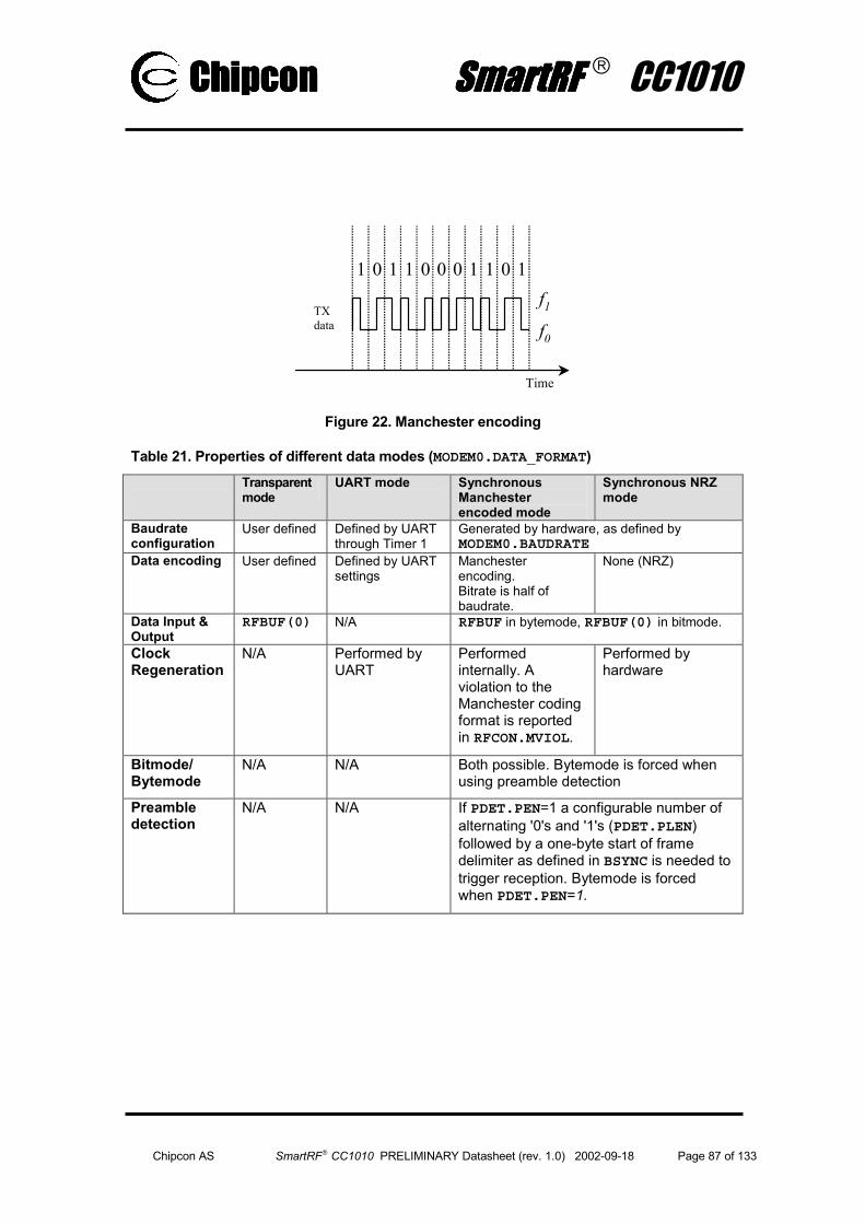
ChipconChipconChipconChipcon SmartRF SmartRF SmartRF SmartRF CC1010
Chipcon AS SmartRF CC1010 PRELIMINARY Datasheet (rev. 1.0) 2002-09-18 Page 87 of 133
Time
TXdata
1 0 1 1 0 0 0 1 1 0 1
f0
f1
Figure 22. Manchester encoding
Table 21. Properties of different data modes (MODEM0.DATA_FORMAT) Transparent
mode UART mode Synchronous
Manchester encoded mode
Synchronous NRZ mode
Baudrate configuration
User defined Defined by UART through Timer 1
Generated by hardware, as defined by MODEM0.BAUDRATE
Data encoding User defined Defined by UART settings
Manchester encoding. Bitrate is half of baudrate.
None (NRZ)
Data Input & Output
RFBUF(0) N/A RFBUF in bytemode, RFBUF(0) in bitmode.
Clock Regeneration
N/A Performed by UART
Performed internally. A violation to the Manchester coding format is reported in RFCON.MVIOL.
Performed by hardware
Bitmode/ Bytemode
N/A N/A Both possible. Bytemode is forced when using preamble detection
Preamble detection
N/A N/A If PDET.PEN=1 a configurable number of alternating '0's and '1's (PDET.PLEN) followed by a one-byte start of frame delimiter as defined in BSYNC is needed to trigger reception. Bytemode is forced when PDET.PEN=1.

ChipconChipconChipconChipcon SmartRF SmartRF SmartRF SmartRF CC1010
Chipcon AS SmartRF CC1010 PRELIMINARY Datasheet (rev. 1.0) 2002-09-18 Page 88 of 133
MODEM0 (0xDB) - Modem Control Register 0 Bit Name R/W Description 7:5 BAUDRATE
(2:0)R/W 000 : 0.6 kBaud
001 : 1.2 kBaud 010 : 2.4 kBaud 011 : 4.8 kBaud 100 : 9.6 kBaud 101 : 19.2, 38.4 and 76.8 kBaud 110 : Not used 111 : Not used
4:3 DATA_FORMAT(1:0)
R/W 00 : NRZ mode 01 : Manchester mode 10 : Transparent mode 11 : UART mode
2:0 XOSC_FREQ(2:0)
R/W Select the current crystal oscillator frequency. 000 : 3-4 MHz, 3.6864 MHz recommended Also used for 76.8 kBaud for 14.7456 MHz and 38.4 kBaud for 7.3728 MHz 001 : 6-8 MHz, 7.3728 MHz recommended Also used for 38.4 kBaud for 14.7456 MHz 010 : 9-12 MHz, 11.0592 MHz recommended Also used for 38.4 kBaud for 22.1184 MHz 011 : 12-16 MHz, 14.7456 MHz recommended 100 : 16-20 MHz, 18.4320 MHz recommended 101 : 20-24 MHz, 22.1184 MHz recommended 110 : Reserved for future use 111 : Reserved for future use
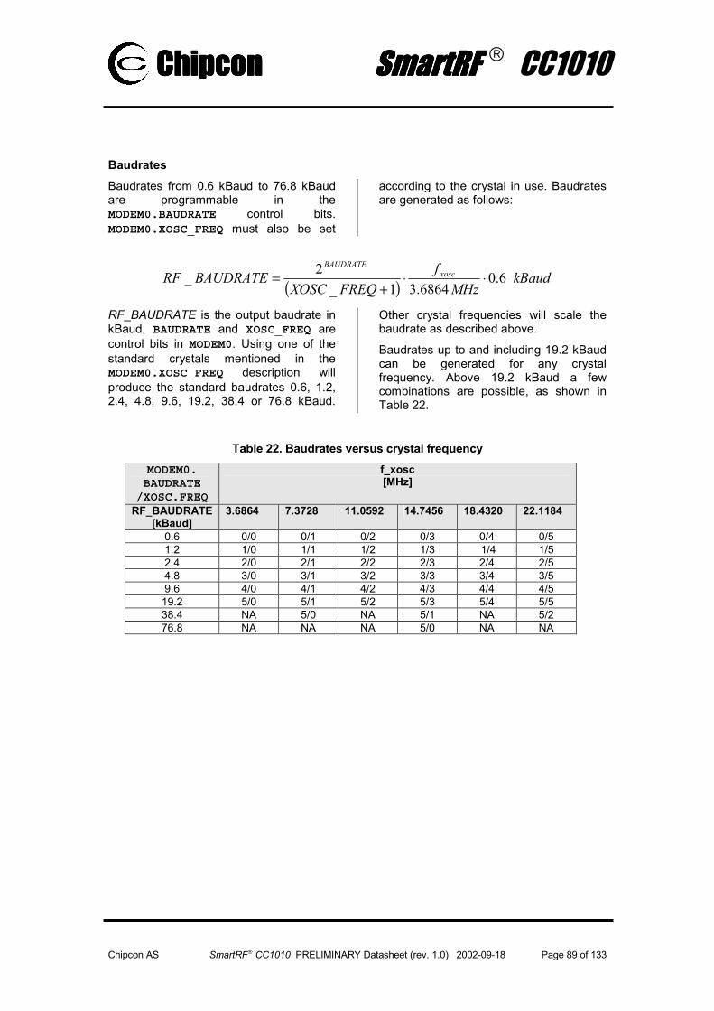
ChipconChipconChipconChipcon SmartRF SmartRF SmartRF SmartRF CC1010
Chipcon AS SmartRF CC1010 PRELIMINARY Datasheet (rev. 1.0) 2002-09-18 Page 89 of 133
BaudratesBaudrates from 0.6 kBaud to 76.8 kBaud are programmable in the MODEM0.BAUDRATE control bits. MODEM0.XOSC_FREQ must also be set
according to the crystal in use. Baudrates are generated as follows:
( ) kBaudMHz
fFREQXOSC
BAUDRATERF xoscBAUDRATE
6.06864.31_
2_ ⋅⋅+
=
RF_BAUDRATE is the output baudrate in kBaud, BAUDRATE and XOSC_FREQ are control bits in MODEM0. Using one of the standard crystals mentioned in the MODEM0.XOSC_FREQ description will produce the standard baudrates 0.6, 1.2, 2.4, 4.8, 9.6, 19.2, 38.4 or 76.8 kBaud.
Other crystal frequencies will scale the baudrate as described above.
Baudrates up to and including 19.2 kBaud can be generated for any crystal frequency. Above 19.2 kBaud a few combinations are possible, as shown in Table 22.
Table 22. Baudrates versus crystal frequency MODEM0.BAUDRATE
/XOSC.FREQ
f_xosc [MHz]
RF_BAUDRATE [kBaud]
3.6864 7.3728 11.0592 14.7456 18.4320 22.1184
0.6 0/0 0/1 0/2 0/3 0/4 0/5 1.2 1/0 1/1 1/2 1/3 1/4 1/5 2.4 2/0 2/1 2/2 2/3 2/4 2/5 4.8 3/0 3/1 3/2 3/3 3/4 3/5 9.6 4/0 4/1 4/2 4/3 4/4 4/5
19.2 5/0 5/1 5/2 5/3 5/4 5/5 38.4 NA 5/0 NA 5/1 NA 5/2 76.8 NA NA NA 5/0 NA NA
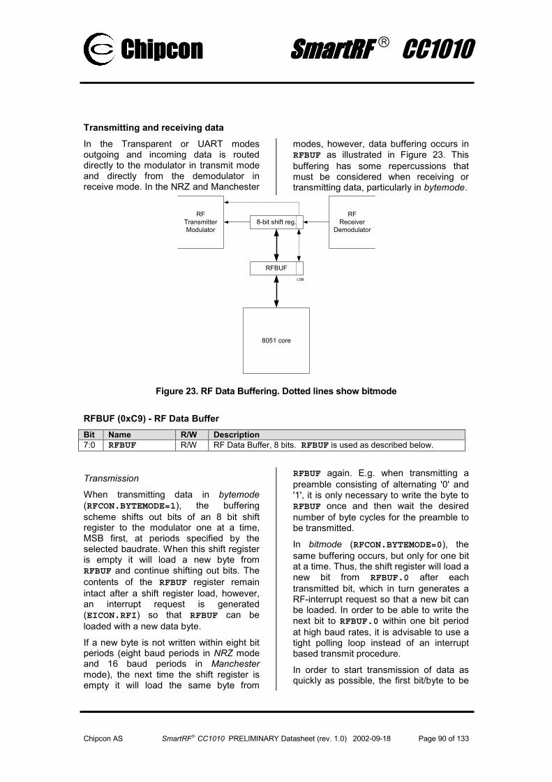
ChipconChipconChipconChipcon SmartRF SmartRF SmartRF SmartRF CC1010
Chipcon AS SmartRF CC1010 PRELIMINARY Datasheet (rev. 1.0) 2002-09-18 Page 90 of 133
Transmitting and receiving data In the Transparent or UART modes outgoing and incoming data is routed directly to the modulator in transmit mode and directly from the demodulator in receive mode. In the NRZ and Manchester
modes, however, data buffering occurs in RFBUF as illustrated in Figure 23. This buffering has some repercussions that must be considered when receiving or transmitting data, particularly in bytemode.
RFBUF
8-bit shift reg.
8051 core
RFTransmitterModulator
RFReceiver
Demodulator
LSB
Figure 23. RF Data Buffering. Dotted lines show bitmode
RFBUF (0xC9) - RF Data Buffer Bit Name R/W Description 7:0 RFBUF R/W RF Data Buffer, 8 bits. RFBUF is used as described below.
Transmission
When transmitting data in bytemode (RFCON.BYTEMODE=1), the buffering scheme shifts out bits of an 8 bit shift register to the modulator one at a time, MSB first, at periods specified by the selected baudrate. When this shift register is empty it will load a new byte from RFBUF and continue shifting out bits. The contents of the RFBUF register remain intact after a shift register load, however, an interrupt request is generated (EICON.RFI) so that RFBUF can be loaded with a new data byte.
If a new byte is not written within eight bit periods (eight baud periods in NRZ mode and 16 baud periods in Manchester mode), the next time the shift register is empty it will load the same byte from
RFBUF again. E.g. when transmitting a preamble consisting of alternating '0' and '1', it is only necessary to write the byte to RFBUF once and then wait the desired number of byte cycles for the preamble to be transmitted.
In bitmode (RFCON.BYTEMODE=0), the same buffering occurs, but only for one bit at a time. Thus, the shift register will load a new bit from RFBUF.0 after each transmitted bit, which in turn generates a RF-interrupt request so that a new bit can be loaded. In order to be able to write the next bit to RFBUF.0 within one bit period at high baud rates, it is advisable to use a tight polling loop instead of an interrupt based transmit procedure.
In order to start transmission of data as quickly as possible, the first bit/byte to be
ChipconChipconChipconChipcon SmartRF SmartRF SmartRF SmartRF CC1010
Chipcon AS SmartRF CC1010 PRELIMINARY Datasheet (rev. 1.0) 2002-09-18 Page 91 of 133
transmitted should be written to RFBUF before the modulator is turned on (RFMAIN.TX_PD=0). It will then be immediately loaded into the shift register and an interrupt request will be generated for the second bit/byte.
It is especially important to take the buffering scheme into account at the end of a transmission. When the last byte of a data frame or packet is loaded into the shift register it is still not transmitted. Thus the interrupt request generated at the same time must not lead to the turning off of either analog or digital parts of the transmit chain. The transmission can not be ended safely until nine bit periods later in bytemode and two bit periods later in bitmode, when the last bit has been shifted out and has propagated through the transmit chain to the antenna. A simple solution is to always transmit two extra bytes in bytemode or two extra bits in bitmode at the end of the real data content. (In bytemode this will result in that approximately seven of these bits will be transmitted along with the real data.)
Reception
When receiving data the buffering scheme works in reverse of what it does during transmitting. Bit by bit from the demodulator is shifted into the eight-bit shift register, MSB-first: When the shift register is full it is loaded into RFBUF and an interrupt request is generated (EICON.RFIF). The byte must be read within one byte period (eight baud periods in NRZ mode and 16 baud periods in Manchester mode). If not, it will be overwritten by the next byte received and data is lost.
In bitmode the same buffering occurs, but only for one bit at a time. Thus, when a new bit arrives from the demodulator the shift register will store it and store the last bit into RFBUF.0, which in turn generates a RF-interrupt request so that the new bit can be read. In order to be able to read the next bit from RFBUF.0 within one bit period at high baud rates it is advisable to use a tight polling loop instead of an interrupt based receive procedure.
No special considerations have to be taken at the start of, or end of, receptions.
ChipconChipconChipconChipcon SmartRF SmartRF SmartRF SmartRF CC1010
Chipcon AS SmartRF CC1010 PRELIMINARY Datasheet (rev. 1.0) 2002-09-18 Page 92 of 133
Demodulation and data decisionA block diagram of the digital demodulator is shown in Figure 24. The IF signal is sampled and it’s instantaneous frequency is detected. The result is decimated and filtered. In the data slicer the data filter output is compared to the average filter output to generate the data output.
The averaging filter is used to find the average value of the incoming data. While the averaging filter is running and acquiring samples, it is important that the number of high and low bits received is equal (e.g. Manchester code or a balanced preamble).
Therefore all modes, also synchronous NRZ mode, need a DC balanced preamble for the internal data slicer to acquire correct comparison level from the averaging filter. The suggested preamble is a ‘010101…’ bit pattern. The same bit pattern should also be used in Manchester mode, giving a ‘011001100110…‘chip’ pattern. This is necessary for the bit synchronizer to synchronize correctly.
The averaging filter must be locked before any NRZ data can be received. This can be done in one of two ways:
• After receiving the preamble and byte synchronisation (see the Synchronization and preamble detection section on page 96), set MODEM1.LOCK_AVG_IN='1' to stop updating the averaging filter.
• Set MODEM1.LOCK_AVG_MODE='1', and then enter Receive mode (RFMAIN.RX_PD=’0’). The averaging filter will then be automatically locked after a preset number of baud periods, programmable in MODEM1.SETTLING. The settling time is programmable from 11 to 86 bauds. The average filter lock status can be read through MODEM1.AVG_FILTER_STAT.
If the averaging filter is locked (MODEM1.LOCK_AVG_MODE='1'), the acquired value will be kept also after Power Down or Transmit mode.
After a modem reset (MODEM1.MODEM_RESET_N), or a main reset (RFMAIN.RESET_N), the averaging filter is reset.
In a polled receiver system the automatic locking can be used. This is illustrated in Figure 25. If the receiver is operated continuously and searching for a preamble, the averaging filter should be locked manually as soon as the preamble is detected. This is shown in Figure 26. If the data is Manchester coded there is no need to lock the averaging filter (MODEM1.LOCK_AVG_IN='0'), as shown in Figure 27.
The minimum length of the preamble depends on the acquisition mode selected and the settling time. Table 23 gives the minimum recommended number of chips for the preamble in NRZ and UART modes. In this context ‘chips’ refer to the data coding. Using Manchester coding every bit consists of two ‘chips’. For Manchester mode the minimum recommended number of chips is shown in Table 24.
A special feature in the data filter is a peak remover acting like a low pass filter. The peak threshold must be programmed according to the deviation and expected frequency drift. When MODEM1.PEAKDETECT is enabled, MODEM2.PLO should be set such that:
85
2
⋅∆+
−=fIF
fIFf
PLOlow
s
low
S
where
1_.0 +
=FREQXOSCMODEM
ff XOSCs
accuracyXTALfkHzIF RFlow _2150 ⋅⋅−=
and ∆f is the deviation. SmartRF® Studio may be used to configure this correctly.
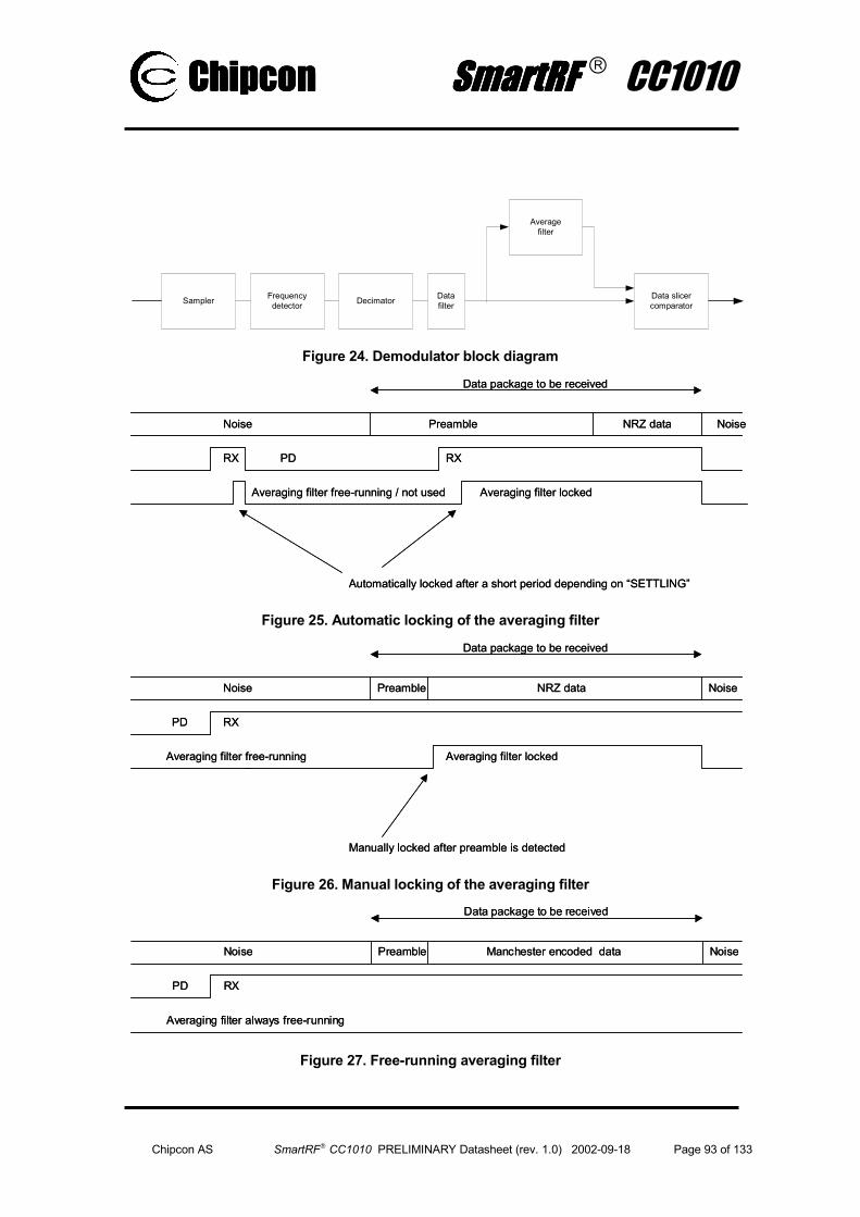
ChipconChipconChipconChipcon SmartRF SmartRF SmartRF SmartRF CC1010
Chipcon AS SmartRF CC1010 PRELIMINARY Datasheet (rev. 1.0) 2002-09-18 Page 93 of 133
Sampler
Averagefilter
DatafilterDecimatorFrequency
detectorData slicercomparator
Figure 24. Demodulator block diagram
Preamble NRZ data
Data package to be received
RX
Noise
RXPD
Averaging filter free-running / not used
Automatically locked after a short period depending on “SETTLING”
Noise
Averaging filter locked
Preamble NRZ data
Data package to be received
RX
Noise
RXPD
Averaging filter free-running / not used
Automatically locked after a short period depending on “SETTLING”
Noise
Averaging filter locked
Figure 25. Automatic locking of the averaging filter
Preamble NRZ data
Data package to be received
RX
Noise
PD
Averaging filter free-running
Manually locked after preamble is detected
Noise
Averaging filter locked
Preamble NRZ data
Data package to be received
RX
Noise
PD
Averaging filter free-running
Manually locked after preamble is detected
Noise
Averaging filter locked
Figure 26. Manual locking of the averaging filter
Preamble Manchester encoded data
Data package to be received
RX
Noise
PD
Averaging filter always free-running
NoisePreamble Manchester encoded data
Data package to be received
RX
Noise
PD
Averaging filter always free-running
Noise
Figure 27. Free-running averaging filter

ChipconChipconChipconChipcon SmartRF SmartRF SmartRF SmartRF CC1010
Chipcon AS SmartRF CC1010 PRELIMINARY Datasheet (rev. 1.0) 2002-09-18 Page 94 of 133
Table 23. Minimum number of bits in the preamble, NRZ and UART mode
Manual Lock Automatic Lock Settling
MODEM1.SETTLING(1:0)
NRZ mode MODEM1.LOCK_AVG_MODE='1' MODEM1.LOCK_AVG_IN='0'=→’1’**
UART mode MODEM1.LOCK_AVG_MODE='1' MODEM1.LOCK_AVG_IN='0'=→’1’**
NRZ mode MODEM1.LOCK_AVG_MODE='0' MODEM1.LOCK_AVG_IN='X'***
UART mode MODEM1.LOCK_AVG_MODE='0' MODEM1.LOCK_AVG_IN='X'***
00 14 11 16 16 01 25 22 32 32 10 46 43 64 64 11 89 86 128 128
Notes: ** The averaging filter is locked when MODEM1.LOCK_AVG_IN is set to 1 *** X = Do not care. The timer for the automatic lock is started when RX mode is set in the RFMAIN register
Table 24. Minimum number of chips in the preamble, Manchester mode
Settling MODEM1.SETTLING(1:0)
Free-running Manchester mode MODEM1.LOCK_AVG_MODE='1' MODEM1.LOCK_AVG_IN='0'
00 23 01 34 10 55 11 98
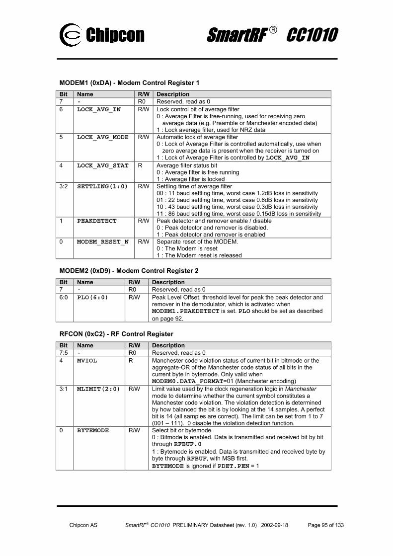
ChipconChipconChipconChipcon SmartRF SmartRF SmartRF SmartRF CC1010
Chipcon AS SmartRF CC1010 PRELIMINARY Datasheet (rev. 1.0) 2002-09-18 Page 95 of 133
MODEM1 (0xDA) - Modem Control Register 1 Bit Name R/W Description 7 - R0 Reserved, read as 0 6 LOCK_AVG_IN R/W Lock control bit of average filter
0 : Average Filter is free-running, used for receiving zero average data (e.g. Preamble or Manchester encoded data)
1 : Lock average filter, used for NRZ data 5 LOCK_AVG_MODE R/W Automatic lock of average filter
0 : Lock of Average Filter is controlled automatically, use when zero average data is present when the receiver is turned on
1 : Lock of Average Filter is controlled by LOCK_AVG_IN 4 LOCK_AVG_STAT R Average filter status bit
0 : Average filter is free running 1 : Average filter is locked
3:2 SETTLING(1:0) R/W Settling time of average filter 00 : 11 baud settling time, worst case 1.2dB loss in sensitivity 01 : 22 baud settling time, worst case 0.6dB loss in sensitivity 10 : 43 baud settling time, worst case 0.3dB loss in sensitivity 11 : 86 baud settling time, worst case 0.15dB loss in sensitivity
1 PEAKDETECT R/W Peak detector and remover enable / disable 0 : Peak detector and remover is disabled. 1 : Peak detector and remover is enabled
0 MODEM_RESET_N R/W Separate reset of the MODEM. 0 : The Modem is reset 1 : The Modem reset is released
MODEM2 (0xD9) - Modem Control Register 2 Bit Name R/W Description 7 - R0 Reserved, read as 0 6:0 PLO(6:0) R/W Peak Level Offset, threshold level for peak the peak detector and
remover in the demodulator, which is activated when MODEM1.PEAKDETECT is set. PLO should be set as described on page 92.
RFCON (0xC2) - RF Control Register Bit Name R/W Description 7:5 - R0 Reserved, read as 0 4 MVIOL R Manchester code violation status of current bit in bitmode or the
aggregate-OR of the Manchester code status of all bits in the current byte in bytemode. Only valid when MODEM0.DATA_FORMAT=01 (Manchester encoding)
3:1 MLIMIT(2:0) R/W Limit value used by the clock regeneration logic in Manchester mode to determine whether the current symbol constitutes a Manchester code violation. The violation detection is determined by how balanced the bit is by looking at the 14 samples. A perfect bit is 14 (all samples are correct). The limit can be set from 1 to 7 (001 – 111). 0 disable the violation detection function.
0 BYTEMODE R/W Select bit or bytemode 0 : Bitmode is enabled. Data is transmitted and received bit by bit through RFBUF.0 1 : Bytemode is enabled. Data is transmitted and received byte by byte through RFBUF, with MSB first. BYTEMODE is ignored if PDET.PEN = 1

ChipconChipconChipconChipcon SmartRF SmartRF SmartRF SmartRF CC1010
Chipcon AS SmartRF CC1010 PRELIMINARY Datasheet (rev. 1.0) 2002-09-18 Page 96 of 133
Synchronization and preamble detectionMost RF communication protocols will have a preamble designated to let the receiver synchronise its reception on a bit and byte level. CC1010 contains hardware that will perform these tasks easily in synchronous NRZ and Manchester encoded modes.
The byte synchronization mechanism ensures that the framing of bytes in the received data bit stream is correct, thus freeing the software from needing to perform shifting and recombination of data bytes. In addition, the synchronization byte functions as a start of frame delimiter. The preamble detection mechanism reduces the workload for the processor when the exact time of the start of a transmission is uncertain. Both mechanisms are active when PDET.PEN is set. (See PDET
register definition below.) Two preamble examples are shown in Figure 28. Note that the Manchester baudrate is twice the NRZ baudrate in the figure.
The preamble must consist of an alternating 0-1-pattern followed by a synchronization byte of any eight bits. Unless the average filter is already locked at the arrival of the synchronization byte in NRZ mode, it is vital that the synchronization byte is DC-balanced (equal number of zeros and ones) and contains no more than two consecutive ones or zeros. It is also required that the synchronization byte contains two consecutive ones or zeros. This means that e.g. 0xCC is not a legal synchronization byte, but 0xC5 is.
NRZ
10100101010
Byte sync
10101 01001
DataPreamble
Bit value
Manchester
1010010101010101 01001Bit value
Figure 28. Preamble detection examples
PDET (0xD3) - Preamble Detection Control Register Bit Name R/W Description 7 PEN R/W Preamble and byte synchronisation enable.
0 : Receiver mode is defined by RFCON.BYTEMODE. 1 : Preamble and byte synchronisation is enabled. RFCON.BYTEMODE is don't care.
6:0 PLEN R/W Preamble length. Define the number of alternating bits required before byte synchronisation. PLEN must be greater than zero.
BSYNC (0xD4) - Byte Synchronisation Register Bit Name R/W Description 7:0 BSYNC(7:0) R/W BSYNC defines the byte which triggers byte synchronisation
during RF preamble detection.

ChipconChipconChipconChipcon SmartRF SmartRF SmartRF SmartRF CC1010
Chipcon AS SmartRF CC1010 PRELIMINARY Datasheet (rev. 1.0) 2002-09-18 Page 97 of 133
The hardware support for preamble detection consists of a seven bit counter, which keeps track of the number of successive alternating bits. It is reset whenever two bits are equal and incremented whenever two successive bits are different. The counter is limited and will not overflow. A seven-bit threshold is programmable through PDET.PLEN. Not before this counter equals or exceeds PDET.PLEN will a synchronization byte be accepted. CC1010 is able to detect preambles (including the synchronization byte) with minimum lengths from 10 to 135 bits.
When the requisite number of alternating zeros and ones has been received, a special state is entered in which a break in the 0-1-pattern is searched for. Once such a break occurs, a synchronization byte matching that defined in BSYNC must occur within a maximum of seven bits, otherwise the receiver will reset its preamble counter and go back to the preamble detection mode.
If, however, a match is found before the timeout, the synchronization byte is transferred to RFBUF and an EXIF.RFIF interrupt request generated, after which the receiver enters normal reception mode. For both the examples shown in Figure 28, BSYNC should be set to 10100101.
PDET.PEN is not cleared by hardware when the preamble is detected, but it will not affect the reception of data. It can be cleared or left set, decided by what is more practical for the software developer. However, before a new preamble detection is initiated, PDET.PEN must be cleared.
If manual average filter locking is performed, the average filter should be locked after receiving the synchronization byte in NRZ mode. (See the Reception section on page 91 for details.) As mentioned above it is vital that the synchronization byte is DC-balanced and contains no more than two consecutive ones or zeros in order to achieve a good average filter lock in this case.
Manchester Violations
In some RF-applications using Manchester coding, violations of the Manchester coding have been used for start- and end-of-frame delimiters. Furthermore some implementations use a sequence of all ones or all zeros for a preamble instead of an alternating zero-one sequence. Although an all zero or all one sequence will certainly be DC-balanced once Manchester coded, the receiver is unable to decide whether it is receiving an all zero or an all one sequence, since only the bit synchronization will separate these.
In order to facilitate reception and transmission of such special cases, support has been implemented in CC1010 for allowing the data format to be changed in the middle of a reception or transmission. Furthermore, violations to the Manchester coding format is reported in the status bit RFCON.MVIOL. The threshold for determining what constitutes a Manchester coding violation can be configured in RFCON.MLIMIT. RFCON.MVIOL is set when, in bitmode, the currently available bit in RFBUF.0 was determined to violate Manchester coding, or in bytemode, when one or more of the bits in the byte currently available in RFBUF were determined to violate the Manchester coding. This can be used, for example, to detect start of frame and end of frame delimiter bytes.
Note that even if RFCON.MVIOL is set when receiving data, RFBUF will still be set to the "best guess" data received. In applications where no Manchester violations are transmitted, it is therefore advisable to ignore RFCON.MVIOL at reception.
In order to be able to send Manchester violations, MODEM0.DATA_FORMAT must be changed to NRZ mode for the byte in question. When in NRZ mode, two bytes must be sent for each Manchester-coded byte. A flagrant violation of Manchester coding could be, for example, the two-byte sequence "11001100"-"00110011". In order to provide this functionality, MODEM0.DATA_FORMAT is buffered in
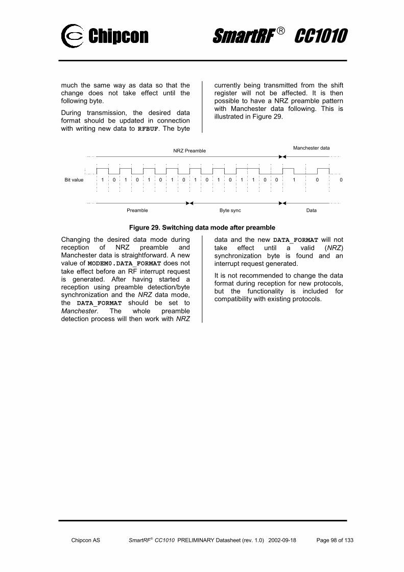
ChipconChipconChipconChipcon SmartRF SmartRF SmartRF SmartRF CC1010
Chipcon AS SmartRF CC1010 PRELIMINARY Datasheet (rev. 1.0) 2002-09-18 Page 98 of 133
much the same way as data so that the change does not take effect until the following byte.
During transmission, the desired data format should be updated in connection with writing new data to RFBUF. The byte
currently being transmitted from the shift register will not be affected. It is then possible to have a NRZ preamble pattern with Manchester data following. This is illustrated in Figure 29.
NRZ Preamble
00110101010
Byte sync
10101 001
DataPreamble
Bit value
Manchester data
Figure 29. Switching data mode after preamble Changing the desired data mode during reception of NRZ preamble and Manchester data is straightforward. A new value of MODEM0.DATA_FORMAT does not take effect before an RF interrupt request is generated. After having started a reception using preamble detection/byte synchronization and the NRZ data mode, the DATA_FORMAT should be set to Manchester. The whole preamble detection process will then work with NRZ
data and the new DATA_FORMAT will not take effect until a valid (NRZ) synchronization byte is found and an interrupt request generated.
It is not recommended to change the data format during reception for new protocols, but the functionality is included for compatibility with existing protocols.
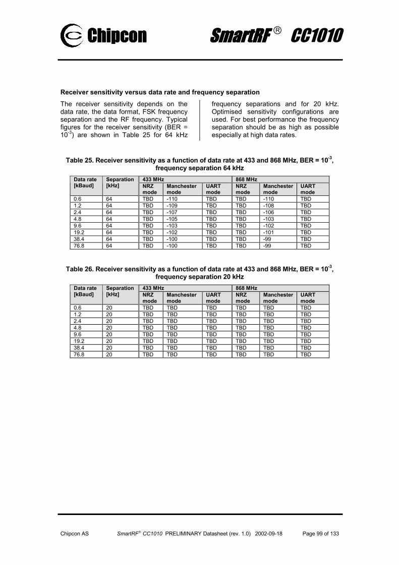
ChipconChipconChipconChipcon SmartRF SmartRF SmartRF SmartRF CC1010
Chipcon AS SmartRF CC1010 PRELIMINARY Datasheet (rev. 1.0) 2002-09-18 Page 99 of 133
Receiver sensitivity versus data rate and frequency separationThe receiver sensitivity depends on the data rate, the data format, FSK frequency separation and the RF frequency. Typical figures for the receiver sensitivity (BER = 10-3) are shown in Table 25 for 64 kHz
frequency separations and for 20 kHz. Optimised sensitivity configurations are used. For best performance the frequency separation should be as high as possible especially at high data rates.
Table 25. Receiver sensitivity as a function of data rate at 433 and 868 MHz, BER = 10-3, frequency separation 64 kHz
433 MHz 868 MHz Data rate [kBaud]
Separation [kHz] NRZ
mode Manchester mode
UART mode
NRZ mode
Manchester mode
UART mode
0.6 64 TBD -110 TBD TBD -110 TBD 1.2 64 TBD -109 TBD TBD -108 TBD 2.4 64 TBD -107 TBD TBD -106 TBD 4.8 64 TBD -105 TBD TBD -103 TBD 9.6 64 TBD -103 TBD TBD -102 TBD 19.2 64 TBD -102 TBD TBD -101 TBD 38.4 64 TBD -100 TBD TBD -99 TBD 76.8 64 TBD -100 TBD TBD -99 TBD
Table 26. Receiver sensitivity as a function of data rate at 433 and 868 MHz, BER = 10-3, frequency separation 20 kHz
433 MHz 868 MHz Data rate [kBaud]
Separation [kHz] NRZ
mode Manchester mode
UART mode
NRZ mode
Manchester mode
UART mode
0.6 20 TBD TBD TBD TBD TBD TBD 1.2 20 TBD TBD TBD TBD TBD TBD 2.4 20 TBD TBD TBD TBD TBD TBD 4.8 20 TBD TBD TBD TBD TBD TBD 9.6 20 TBD TBD TBD TBD TBD TBD 19.2 20 TBD TBD TBD TBD TBD TBD 38.4 20 TBD TBD TBD TBD TBD TBD 76.8 20 TBD TBD TBD TBD TBD TBD
ChipconChipconChipconChipcon SmartRF SmartRF SmartRF SmartRF CC1010
Chipcon AS SmartRF CC1010 PRELIMINARY Datasheet (rev. 1.0) 2002-09-18 Page 100 of 133
Frequency programmingThe frequency synthesiser (PLL) is controlled by the frequency word in the configuration registers. There are two frequency words, A and B, which can be programmed to two different frequencies. One of the frequency words can be used for RX (local oscillator frequency) and other for TX (transmitting frequency, f0). This makes it possible to switch very fast between RX mode and TX mode. They can also be used for RX (or TX) at two different channels. Frequency word A or B is selected by the RFMAIN.F_REG control bit.
The frequency word, FREQ, is 24 bits (3 bytes) located in FREQ_2A:FREQ_1A:FREQ_0A and FREQ_2B:FREQ_1B:FREQ_0B for the A and B word, respectively.
The FSK frequency separation (two times the deviation), FSEP, is programmed in the FSEP1:FSEP0 registers (11 bits).
The frequency word FREQ can be calculated from:
163848192+⋅+⋅= TXDATAFSEPFREQff refVCO
where TXDATA is 0 or 1 in transmit mode depending on the data bit to be transmitted. In receive mode TXDATA is always 0.
The reference frequency fref is the crystal oscillator clock divided by PLL.REFDIV, a number between 2 and 24 such that:
1.00 MHz ≤ REFDIV ≤ 2.40 MHz
Thus, the reference frequency fref is:
REFDIVf
f xoscref =
fVCO is the Local Oscillator (LO) frequency for receive mode, and the f0 frequency for transmit mode (lower FSK frequency).
The LO frequency must be fRF – fIF or fRF + fIF giving a low-side or high side LO injection respectively. Note that the data in RFBUF will be inverted if high-side LO is used. Do also note that the fIF depend on the RF frequency (150 and 130 kHz for 433 and 868 MHz respectively).
The upper FSK transmit frequency is given by:
f1 = f0 + fsep
where the frequency separation fsep is set by the 11 bit separation word (FSEP1:FSEP0):
16384FSEPff refsep ⋅=
Clearing PLL.ALARM_DISABLE will enable generation of the frequency alarm bits PLL.ALARM_H and PLL.ALARM_L. These bits indicate that the frequency synthesis PLL is unable to generate the frequency requested, and the PLL should be recalibrated as described in the VCO and PLL self-calibration section on page 105.
Chipcon recommends using the frequency settings described in the Recommended Settings for ISM Frequencies section on page 103.
FREQ_2A (0xCC) – Frequency A, Control Register 2 Bit Name R/W Description 7:0 FREQ_A
(23:16)R/W 8 MSB of frequency control word A. It must be programmed such
that FREQ_2A ≥ 01000000
FREQ_1A (0xCB) – Frequency A, Control Register 1 Bit Name R/W Description 7:0 FREQ_A
(15:8)R/W Bit 15 to 8 of frequency control word A.
ChipconChipconChipconChipcon SmartRF SmartRF SmartRF SmartRF CC1010
Chipcon AS SmartRF CC1010 PRELIMINARY Datasheet (rev. 1.0) 2002-09-18 Page 101 of 133
FREQ_0A (0xCA) – Frequency A, Control Register 0 Bit Name R/W Description 7:0 FREQ_A(7:0) R/W 8 LSB of frequency control word A.
FREQ_2B (0xCF) - Frequency B, Control Register 2 Bit Name R/W Description 7:0 FREQ_B
(23:16)R/W 8 MSB of frequency control word B. It must be programmed such
that FREQ_2B ≥ 01000000
FREQ_1B (0xCE) - Frequency B, Control Register 1 Bit Name R/W Description 7:0 FREQ_B
(15:8)R/W Bit 15 to 8 of frequency control word B.
FREQ_0B (0xCD) - Frequency B, Control Register 0 Bit Name R/W Description 7:0 FREQ_B(7:0) R/W 8 LSB of frequency control word B.
FSEP1 (0xEB) - Frequency Separation Control Register 1 Bit Name R/W Description 7:3 - R0 Reserved, read as 0 2:0 FSEP(10:8) R/W 3 MSB of the frequency separation control word FSEP
FSEP0 (0xEA) - Frequency Separation Control Register 0 Bit Name R/W Description 7:0 FSEP(7:0) R/W 8 LSB of the frequency separation control word FSEP
PLL (0xE3) - PLL Control Register Bit Name R/W Description 7:3 REFDIV(4:0) R/W Reference divider setting. The main crystal oscillator frequency is
divided by REFDIV to create the RF reference frequency fref. Valid REFDIV settings are 2 through 24, as described above.
2 ALARM_DISABLE
R/W Disable / Enable the generation of the ALARM_H and ALARM_L bits 0 : Alarm function enabled 1 : Alarm function disabled
1 ALARM_H R Status bit for tuning voltage out of range (too close to VDD) The PLL should be re-calibrated if this bit is set
0 ALARM_L R Status bit for tuning voltage out of range (too close to GND) The PLL should be re-calibrated if this bit is set
ChipconChipconChipconChipcon SmartRF SmartRF SmartRF SmartRF CC1010
Chipcon AS SmartRF CC1010 PRELIMINARY Datasheet (rev. 1.0) 2002-09-18 Page 102 of 133
Lock IndicationThe frequency synthesis PLL has a lock indicator which can be read from the LOCK register. LOCK_INSTANT is a single sample of the phase difference between the reference frequency and the divided VCO frequency. This bit gives a lock accuracy of > 25 %, depending on the division ratio set by the FREQ registers. To be used as a lock indicator, this bit must be sampled over a period of time to increase the accuracy.
Otherwise LOCK_CONTINUOUS should be used. It is a filtered version of LOCK_INSTANT, giving a lock accuracy of 99.3 % with PLL_LOCK_ACCURACY cleared.
If lock is not achieved, the PLL should be recalibrated as described on page 105.
LOCK (0xE4) - PLL Lock Register Bit Name R/W Description 7:4 - R0 Reserved, read as 0 3 PLL_LOCK_ACCURACY R/W 0 : Sets Lock Threshold = 127, Reset Lock Threshold =
111 for continuous lock. Corresponds to a worst case accuracy of 99.3%
1 : Sets Lock Threshold = 31, Reset Lock Threshold =15 for continuous lock. Corresponds to a worst case accuracy of 97.2%
2 PLL_LOCK_LENGTH R/W 0 : Normal PLL lock window 1 : Not used
1 LOCK_INSTANT R Status bit from Lock Detector. The result of one sample of the lock window on the PLL reference clock
0 LOCK_CONTINUOUS R Status bit from Lock Detector, set according to the PLL_LOCK_ACCURACY setting

ChipconChipconChipconChipcon SmartRF SmartRF SmartRF SmartRF CC1010
Chipcon AS SmartRF CC1010 PRELIMINARY Datasheet (rev. 1.0) 2002-09-18 Page 103 of 133
Recommended Settings for ISM FrequenciesThe recommended frequency synthesiser settings for a few operating frequencies in the popular ISM bands are shown in Table 27. These settings ensure optimum configuration of the synthesiser in receive mode for best sensitivity. For some settings of the synthesiser (combinations of RF frequencies and reference frequency), the receiver sensitivity is degraded. The performance of the
transmitter is not affected by the settings, but recommended transmitter settings are included for completeness. The FSK frequency separation is set to 64 kHz. The SmartRF Studio can be used to generate the optimised configuration data as well. Also an application note (AN011) and a spreadsheet are available from Chipcon generating configuration data for any frequency giving optimum sensitivity.
ISM Frequency [MHz]
Actual frequency [MHz]
Crystal frequency [MHz]
Low-side / high- side LO*
Reference divider REFDIV [decimal]
Frequency word RX Mode FREQ [decimal]
Frequency word RX mode FREQ [hex]
315 315.337200 3.6864 Low-side 3 4194304 400000 7.3728 6 4194304 400000 11.0592 9 4194304 400000 14.7456 12 4194304 400000 18.4320 15 4194304 400000 22.1184 18 4194304 400000
3.6864 3 5767168 580000 7.3728 6 5767168 580000 11.0592 9 5767168 580000 14.7456 12 5767168 580000 18.4320 15 5767168 580000
433.3 433.302000
22.1184
Low-side
18 5767168 580000 433.9 433.916400 3.6864 Low-side 3 5775360 582000 7.3728 6 5775360 582000 11.0592 9 5775360 582000 14.7456 12 5775360 582000 18.4320 15 5775360 582000 22.1184 18 5775360 582000 434.5 434.530800 3.6864 Low-side 3 5783552 584000 7.3728 6 5783552 584000 11.0592 9 5783552 584000 14.7456 12 5783552 584000 18.4320 15 5783552 584000 22.1184 18 5783552 584000 868.3 868.277200 3.6864 Low-side 3 7708672 75A000 7.3728 6 7708672 75A000 11.0592 9 7708672 75A000 14.7456 12 7708672 75A000 18.4320 15 7708672 75A000 22.1184 18 7708672 75A000 868.95 868.938800 3.6864 High-side 3 7716864 75C000 7.3728 6 7716864 75C000 11.0592 9 7716864 75C000 14.7456 12 7716864 75C000 18.4320 15 7716864 75C000 22.1184 18 7716864 75C000
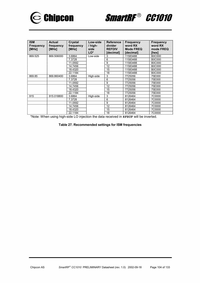
ChipconChipconChipconChipcon SmartRF SmartRF SmartRF SmartRF CC1010
Chipcon AS SmartRF CC1010 PRELIMINARY Datasheet (rev. 1.0) 2002-09-18 Page 104 of 133
ISM Frequency [MHz]
Actual frequency [MHz]
Crystal frequency [MHz]
Low-side / high- side LO*
Reference divider REFDIV [decimal]
Frequency word RX Mode FREQ [decimal]
Frequency word RX mode FREQ [hex]
869.525 869.506000 3.6864 Low-side 3 11583488 B0C000 7.3728 6 11583488 B0C000 11.0592 9 11583488 B0C000 14.7456 12 11583488 B0C000 18.4320 15 11583488 B0C000 22.1184 18 11583488 B0C000 869.85 869.860400 3.6864 High-side 3 7725056 75E000 7.3728 6 7725056 75E000 11.0592 9 7725056 75E000 14.7456 12 7725056 75E000 18.4320 15 7725056 75E000 22.1184 18 7725056 75E000 915 915.018800 3.6864 High-side 3 8126464 7C0000 7.3728 6 8126464 7C0000 11.0592 9 8126464 7C0000 14.7456 12 8126464 7C0000 18.4320 15 8126464 7C0000 22.1184 18 8126464 7C0000 *Note: When using high-side LO injection the data received in RFBUF will be inverted.
Table 27. Recommended settings for ISM frequencies

ChipconChipconChipconChipcon SmartRF SmartRF SmartRF SmartRF CC1010
Chipcon AS SmartRF CC1010 PRELIMINARY Datasheet (rev. 1.0) 2002-09-18 Page 105 of 133
VCO Only one external inductor (L101) is required for the VCO. The inductor will determine the operating frequency range of the circuit. It is important to place the inductor as close to the pins as possible in order to reduce stray inductance. It is recommended to use a high Q, low tolerance inductor for best performance.
Typical tuning range for the integrated varactor is 20-25%.
Component values for various frequencies are given in Table 20. Component values for other frequencies can be found using the SmartRF® Studio software.
VCO and PLL self-calibration To compensate for supply voltage, temperature and process variations the VCO and PLL must be calibrated. The calibration is done automatically and sets optimum VCO tuning range and optimum charge pump current for PLL stability. The calibration is controlled by using the CAL register.
After setting up the device at the operating frequency, the TEST6 register must be programmed (depend on operation mode). Then the self-calibration is initiated by setting the CAL.CAL_START bit. The calibration result is stored internally in the chip, and is valid as long as power is not turned off. If large supply voltage variations (more than 0.5 V) or temperature variations (more than 40 degrees) occur after calibration, a new calibration should be performed. For more details on the calibration data, see the description for test and calibration registers page 118.
When CAL.CAL_WAIT = 1 the calibration is complete and the CAL.CAL_COMPLETE flag is set after 25650 reference clock cycles (fREF, see the Frequency programming section at page 100). The user can poll this bit, or simply wait 25650 reference clock cycles. The lowest permitted reference frequency (1 MHz) gives a wait time of 25.65 ms, which is the worst case. Some calibration times for different reference frequencies are listed in Table 28. When CAL.CAL_WAIT = 0 it takes 12825 cycles, but this is not recommended.
Table 28. Calibration times Reference frequency
[MHz] Calibration time
[ms]
2.4 10.69
2.0 12.83
1.5 17.10
1.0 25.65
The CAL_START bit must be cleared after the calibration is done. This will also clear the CAL.CAL_COMPLETE status bit.
There are separate calibration values for the two frequency registers. If the two frequencies, A and B, differ more than 1 MHz, or different VCO currents are used (CURRENT.VCO_CURRENT(3:0)), the calibration should be done separately. When using a 10.7 MHz external IF the LO is 10.7 MHz below/above the transmit frequency, hence separate calibration must be done. The CAL.CAL_DUAL bit controls dual or separate calibration.
The single frequency calibration algorithm using separate calibration for RX and TX frequency is illustrated in Figure 30.
In Figure 31 the dual calibration algorithm is shown for two RX frequencies. It could also be used for two TX frequencies, or even for one RX and one TX frequency if the same VCO current is used.
In multi-channel and frequency hopping applications the PLL calibration values may be read and stored for later use. By reading back calibration values and frequency change can be done without
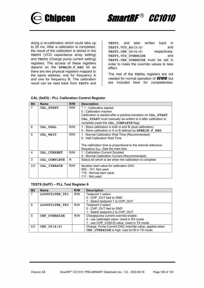
ChipconChipconChipconChipcon SmartRF SmartRF SmartRF SmartRF CC1010
Chipcon AS SmartRF CC1010 PRELIMINARY Datasheet (rev. 1.0) 2002-09-18 Page 106 of 133
doing a re-calibration which could take up to 25 ms. After a calibration is completed, the result of the calibration is stored in the TEST0 (VCO capacitance array setting) and TEST2 (Charge pump current setting) registers. The access of these registers depend on the RFMAIN.F_REG bit as there are two physical registers mapped to the same address, one for frequency A and one for frequency B. The calibration result can be read back from TEST0 and
TEST2, and later written back in TEST5.VCO_AO(3:0) and TEST5.CHP_CO(4:0) respectively. TEST5.VCO_OVERRIDE and TEST6.CHP_OVERRIDE must be set in order to make the override values to take effect.
The rest of the TESTn registers are not needed for normal operation of CC1010, but are included here for completeness.
CAL (0xE5) - PLL Calibration Control Register Bit Name R/W Description 7 CAL_START R/W ↑ 1 : Calibration started
0 : Calibration inactive Calibration is started after a positive transition on CAL_START. CAL_START must manually be written to 0 after calibration is complete (read the CAL_COMPLETE flag)
6 CAL_DUAL R/W 1 : Store calibration in both A and B (dual calibration) 0 : Store calibration in A or B defined by RFMAIN.F_REG
5 CAL_WAIT R/W 1 : Normal Calibration Wait Time (Recommended) 0 : Half Calibration Wait Time The calibration time is proportional to the internal reference frequency fREF. See the main text.
4 CAL_CURRENT R/W 1 : Calibration Current Doubled 0 : Normal Calibration Current (Recommended)
3 CAL_COMPLETE R Status bit which is set when the calibration is complete
2:0 CAL_ITERATE R/W Iteration start value for calibration DAC 000 - 101: Not used 110 : Normal start value 111 : Not used
TEST6 (0xFF) – PLL Test Register 6 Bit Name R/W Description 7 LOOPFILTER_TP1 R/W Testpoint 1 select
0 : CHP_OUT tied to GND 1 : Select testpoint 1 to CHP_OUT
6 LOOPFILTER_TP2 R/W Testpoint 2 select 0 : CHP_OUT tied to GND 1 : Select testpoint 2 to CHP_OUT
5 CHP_OVERRIDE R/W Chargepump current override enable 0 : use calibrated value. Used in RX mode 1 : use CHP_CO[4:0] value. Used in TX mode
4:0 CHP_CO(4:0) Charge_Pump Current DAC override value, applied when CHP_OVERRIDE is high. Use 0x1B in TX mode.

ChipconChipconChipconChipcon SmartRF SmartRF SmartRF SmartRF CC1010
Chipcon AS SmartRF CC1010 PRELIMINARY Datasheet (rev. 1.0) 2002-09-18 Page 107 of 133
TEST5 (0xFE) – PLL Test Register 5 Bit Name R/W Description 7:6 - R0 Reserved, read as 0 5 CHP_DISABLE R/W PLL Charge Pump disable
0 : Charge Pump is enabled (normal function) 1 : Charge Pump is disabled
4 VCO_OVERRIDE R/W VCO array override 0 : VCO array is not overridden (normal function) 1 : VCO array is set by VCO_AO(3:0)
3:0 VCO_AO(3:0) R/W VCO Array override value
TEST4 (0xFD) – PLL Test Register 4 Bit Name R/W Description 7:6 - R/W Reserved, read as 0 5:0 L2KIO R/W Constant charge pump current scaling / rounding factor. Sets
bandwidth of PLL. Default value is 0x25 and shall be used for all modes
TEST3 (0xFC) – PLL Test Register 3 Bit Name R/W Description 7:5 - R0 Reserved, read as 0 4 BREAK_LOOP R/W Break frequency synthesis PLL
0 : PLL loop closed (normal operation) 1 : PLL loop open
3:0 CAL_DAC_OPEN(3:0)
R/W Calibration DAC override value, active when BREAK_LOOP is set
TEST2 (0xFB) – PLL Test Register 2 Bit Name R/W Description 7:5 - R0 Reserved, read as 0 4:0 CHP_CURRENT
(4:0)R Status vector defining the applied charge pump current
TEST1 (0xFA) – PLL Test Register 1 Bit Name R/W Description 7:4 - R0 Reserved, read as 0 3:0 CAL_DAC(3:0) R Status vector defining the applied calibration DAC value
TEST0 (0xF9) – PLL Test Register 0 Bit Name R/W Description 7:4 - R0 Reserved, read as 0 3:0 VCO_ARRAY(3:0) R Status vector defining the applied VCO array
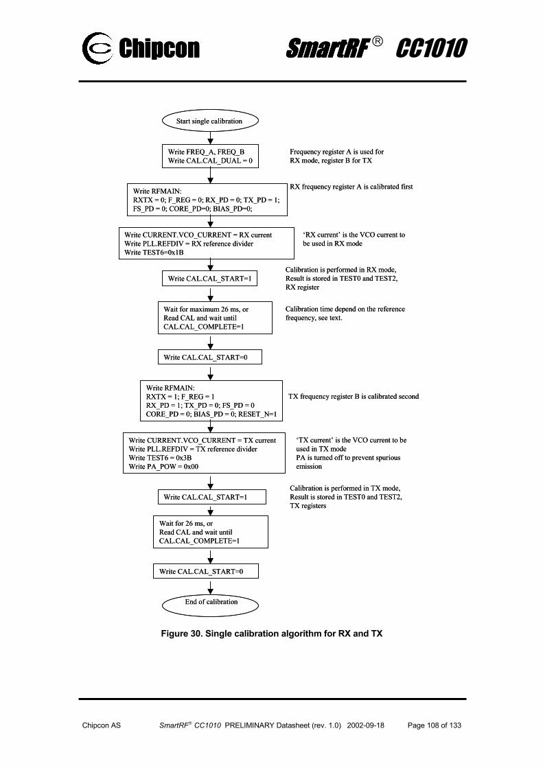
ChipconChipconChipconChipcon SmartRF SmartRF SmartRF SmartRF CC1010
Chipcon AS SmartRF CC1010 PRELIMINARY Datasheet (rev. 1.0) 2002-09-18 Page 108 of 133
Write CAL.CAL_START=0
End of calibration
Wait for maximum 26 ms, or Read CAL and wait until CAL.CAL_COMPLETE=1
Start single calibration
RX frequency register A is calibrated firstWrite RFMAIN:RXTX = 0; F_REG = 0; RX_PD = 0; TX_PD = 1; FS_PD = 0; CORE_PD=0; BIAS_PD=0;
Write FREQ_A, FREQ_BWrite CAL.CAL_DUAL = 0
Frequency register A is used for RX mode, register B for TX
Write CAL.CAL_START=1Calibration is performed in RX mode,Result is stored in TEST0 and TEST2,RX register
Write CURRENT.VCO_CURRENT = RX currentWrite PLL.REFDIV = RX reference dividerWrite TEST6=0x1B
‘RX current’ is the VCO current to be used in RX mode
Write CAL.CAL_START=0
Wait for 26 ms, or Read CAL and wait until CAL.CAL_COMPLETE=1
TX frequency register B is calibrated secondWrite RFMAIN:RXTX = 1; F_REG = 1RX_PD = 1; TX_PD = 0; FS_PD = 0CORE_PD = 0; BIAS_PD = 0; RESET_N=1
Write CAL.CAL_START=1Calibration is performed in TX mode,Result is stored in TEST0 and TEST2, TX registers
Write CURRENT.VCO_CURRENT = TX currentWrite PLL.REFDIV = TX reference dividerWrite TEST6 = 0x3BWrite PA_POW = 0x00
‘TX current’ is the VCO current to be used in TX modePA is turned off to prevent spurious emission
Calibration time depend on the reference frequency, see text.
Write CAL.CAL_START=0
End of calibration
Wait for maximum 26 ms, or Read CAL and wait until CAL.CAL_COMPLETE=1
Start single calibration
RX frequency register A is calibrated firstWrite RFMAIN:RXTX = 0; F_REG = 0; RX_PD = 0; TX_PD = 1; FS_PD = 0; CORE_PD=0; BIAS_PD=0;
Write FREQ_A, FREQ_BWrite CAL.CAL_DUAL = 0
Frequency register A is used for RX mode, register B for TX
Write CAL.CAL_START=1Calibration is performed in RX mode,Result is stored in TEST0 and TEST2,RX register
Write CURRENT.VCO_CURRENT = RX currentWrite PLL.REFDIV = RX reference dividerWrite TEST6=0x1B
‘RX current’ is the VCO current to be used in RX mode
Write CAL.CAL_START=0
Wait for 26 ms, or Read CAL and wait until CAL.CAL_COMPLETE=1
TX frequency register B is calibrated secondWrite RFMAIN:RXTX = 1; F_REG = 1RX_PD = 1; TX_PD = 0; FS_PD = 0CORE_PD = 0; BIAS_PD = 0; RESET_N=1
Write CAL.CAL_START=1Calibration is performed in TX mode,Result is stored in TEST0 and TEST2, TX registers
Write CURRENT.VCO_CURRENT = TX currentWrite PLL.REFDIV = TX reference dividerWrite TEST6 = 0x3BWrite PA_POW = 0x00
‘TX current’ is the VCO current to be used in TX modePA is turned off to prevent spurious emission
Calibration time depend on the reference frequency, see text.
Figure 30. Single calibration algorithm for RX and TX
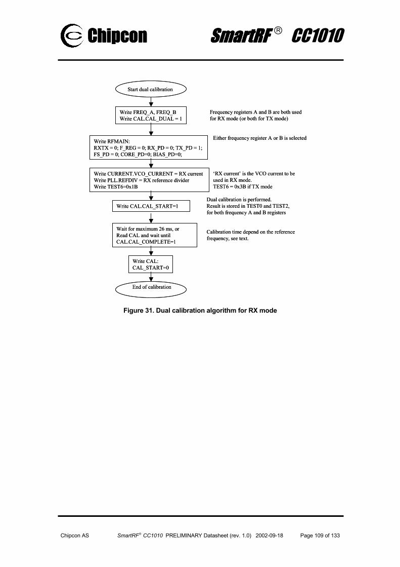
ChipconChipconChipconChipcon SmartRF SmartRF SmartRF SmartRF CC1010
Chipcon AS SmartRF CC1010 PRELIMINARY Datasheet (rev. 1.0) 2002-09-18 Page 109 of 133
Write CAL:CAL_START=0
End of calibration
Wait for maximum 26 ms, or Read CAL and wait until CAL.CAL_COMPLETE=1
Start dual calibration
Either frequency register A or B is selectedWrite RFMAIN:RXTX = 0; F_REG = 0; RX_PD = 0; TX_PD = 1; FS_PD = 0; CORE_PD=0; BIAS_PD=0;
Write FREQ_A, FREQ_BWrite CAL.CAL_DUAL = 1
Frequency registers A and B are both used for RX mode (or both for TX mode)
Write CAL.CAL_START=1Dual calibration is performed.Result is stored in TEST0 and TEST2,for both frequency A and B registers
Write CURRENT.VCO_CURRENT = RX currentWrite PLL.REFDIV = RX reference dividerWrite TEST6=0x1B
‘RX current’ is the VCO current to be used in RX mode. TEST6 = 0x3B if TX mode
Calibration time depend on the reference frequency, see text.
Figure 31. Dual calibration algorithm for RX mode
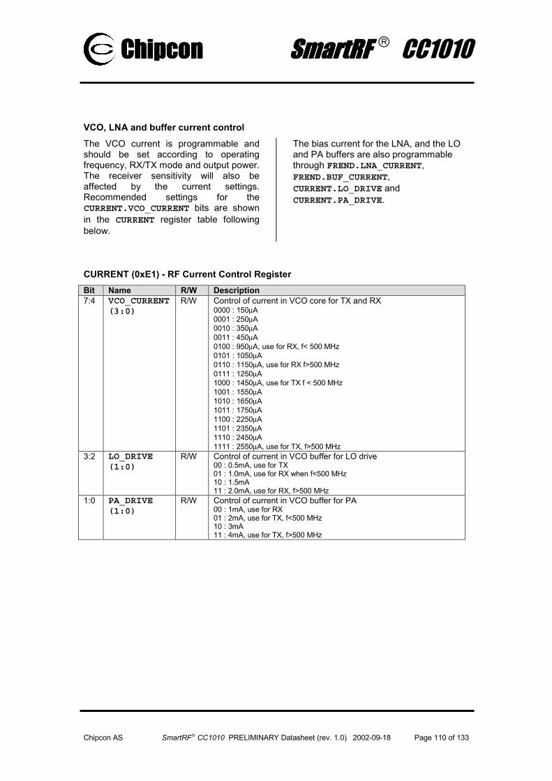
ChipconChipconChipconChipcon SmartRF SmartRF SmartRF SmartRF CC1010
Chipcon AS SmartRF CC1010 PRELIMINARY Datasheet (rev. 1.0) 2002-09-18 Page 110 of 133
VCO, LNA and buffer current controlThe VCO current is programmable and should be set according to operating frequency, RX/TX mode and output power. The receiver sensitivity will also be affected by the current settings. Recommended settings for the CURRENT.VCO_CURRENT bits are shown in the CURRENT register table following below.
The bias current for the LNA, and the LO and PA buffers are also programmable through FREND.LNA_CURRENT, FREND.BUF_CURRENT, CURRENT.LO_DRIVE and CURRENT.PA_DRIVE.
CURRENT (0xE1) - RF Current Control Register Bit Name R/W Description 7:4 VCO_CURRENT
(3:0)R/W Control of current in VCO core for TX and RX
0000 : 150µA 0001 : 250µA 0010 : 350µA 0011 : 450µA 0100 : 950µA, use for RX, f< 500 MHz 0101 : 1050µA 0110 : 1150µA, use for RX f>500 MHz 0111 : 1250µA 1000 : 1450µA, use for TX f < 500 MHz 1001 : 1550µA 1010 : 1650µA 1011 : 1750µA 1100 : 2250µA 1101 : 2350µA 1110 : 2450µA 1111 : 2550µA, use for TX, f>500 MHz
3:2 LO_DRIVE(1:0)
R/W Control of current in VCO buffer for LO drive 00 : 0.5mA, use for TX 01 : 1.0mA, use for RX when f<500 MHz 10 : 1.5mA 11 : 2.0mA, use for RX, f>500 MHz
1:0 PA_DRIVE(1:0)
R/W Control of current in VCO buffer for PA 00 : 1mA, use for RX 01 : 2mA, use for TX, f<500 MHz 10 : 3mA 11 : 4mA, use for TX, f>500 MHz

ChipconChipconChipconChipcon SmartRF SmartRF SmartRF SmartRF CC1010
Chipcon AS SmartRF CC1010 PRELIMINARY Datasheet (rev. 1.0) 2002-09-18 Page 111 of 133
FREND (0xEE) - Front End Control Register Bit Name R/W Description 7:6 - R/W Reserved, should always be written 0 5 BUF_CURRENT R/W Control of current in the LNA_FOLLOWER
0 : 520uA, use for f<500 MHz 1 : 690uA, use for f>500 MHz
4:3 LNA_CURRENT(1:0)
R/W Control of current in LNA 00 : 0.8mA 01 : 1.4mA, use for f<500 MHz 10 : 1.8mA, use for f>500 MHz 11 : 2.2mA
2 IF_EXTERNAL R/W Controls where the output from the mixer goes: 0: To internal IF filter and demodulator 1: To the AD2(RSSI/IF) pin for external filtering and demodulation
1 RSSI R/W 0: RSSI output disconnected from AD2(RSSI/IF)pin 1: RSSI output connected to AD2(RSSI/IF)pin
0 - R/W Reserved, should always be written 0
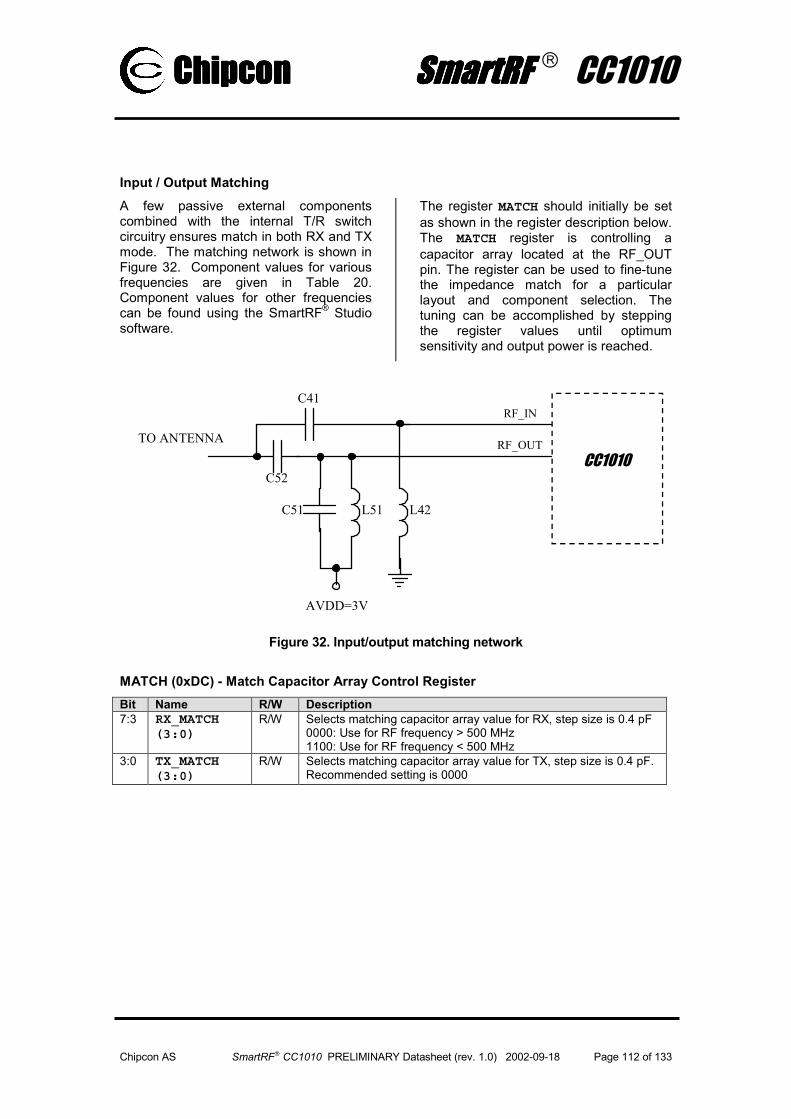
ChipconChipconChipconChipcon SmartRF SmartRF SmartRF SmartRF CC1010
Chipcon AS SmartRF CC1010 PRELIMINARY Datasheet (rev. 1.0) 2002-09-18 Page 112 of 133
Input / Output MatchingA few passive external components combined with the internal T/R switch circuitry ensures match in both RX and TX mode. The matching network is shown in Figure 32. Component values for various frequencies are given in Table 20. Component values for other frequencies can be found using the SmartRF® Studio software.
The register MATCH should initially be set as shown in the register description below. The MATCH register is controlling a capacitor array located at the RF_OUT pin. The register can be used to fine-tune the impedance match for a particular layout and component selection. The tuning can be accomplished by stepping the register values until optimum sensitivity and output power is reached.
RF_IN
RF_OUTTO ANTENNA
CC1010
L51C51
C52
AVDD=3V
L42
C41
Figure 32. Input/output matching network
MATCH (0xDC) - Match Capacitor Array Control Register Bit Name R/W Description 7:3 RX_MATCH
(3:0)R/W Selects matching capacitor array value for RX, step size is 0.4 pF
0000: Use for RF frequency > 500 MHz 1100: Use for RF frequency < 500 MHz
3:0 TX_MATCH(3:0)
R/W Selects matching capacitor array value for TX, step size is 0.4 pF. Recommended setting is 0000
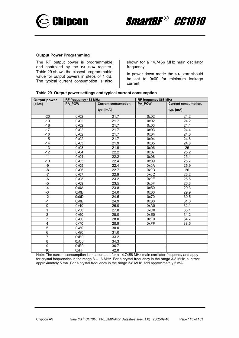
ChipconChipconChipconChipcon SmartRF SmartRF SmartRF SmartRF CC1010
Chipcon AS SmartRF CC1010 PRELIMINARY Datasheet (rev. 1.0) 2002-09-18 Page 113 of 133
Output Power ProgrammingThe RF output power is programmable and controlled by the PA_POW register. Table 29 shows the closest programmable value for output powers in steps of 1 dB. The typical current consumption is also
shown for a 14.7456 MHz main oscillator frequency.
In power down mode the PA_POW should be set to 0x00 for minimum leakage current.
Table 29. Output power settings and typical current consumption RF frequency 433 MHz RF frequency 868 MHz Output power
[dBm] PA_POW Current consumption,
typ. [mA]
PA_POW Current consumption,
typ. [mA]
-20 0x02 21.7 0x02 24.2 -19 0x02 21.7 0x02 24.2 -18 0x02 21.7 0x03 24.4 -17 0x02 21.7 0x03 24.4 -16 0x02 21.7 0x04 24.6 -15 0x02 21.7 0x04 24.6 -14 0x03 21.9 0x05 24.8 -13 0x03 21.9 0x06 25 -12 0x04 22.2 0x07 25.2 -11 0x04 22.2 0x08 25.4 -10 0x05 22.4 0x09 25.7 -9 0x05 22.4 0x0A 25.9 -8 0x06 22.7 0x0B 26 -7 0x07 22.9 0x0C 26.2 -6 0x08 23.2 0x0E 26.6 -5 0x09 23.5 0x0F 26.8 -4 0x0A 23.8 0x50 29.3 -3 0x0B 24.0 0x60 29.9 -2 0x0D 24.5 0x70 30.5 -1 0x0E 24.9 0x80 31.0 0 0x40 26.0 0xA0 32.1 1 0x50 27.0 0xC0 33.1 2 0x60 28.0 0xE0 34.2 3 0x60 28.0 0xF0 34.7 4 0x70 28.9 0xFF 38.5 5 0x80 30.0 6 0x90 31.0 7 0xB0 33.2 8 0xC0 34.3 9 0xE0 36.7
10 0xFF 42.8 Note: The current consumption is measured at for a 14.7456 MHz main oscillator frequency and appy for crystal frequencies in the range 8 – 16 MHz. For a crystal frequency in the range 3-8 MHz, subtract approximately 5 mA. For a crystal frequency in the range 3-8 MHz, add approximately 5 mA.

ChipconChipconChipconChipcon SmartRF SmartRF SmartRF SmartRF CC1010
Chipcon AS SmartRF CC1010 PRELIMINARY Datasheet (rev. 1.0) 2002-09-18 Page 114 of 133
PA_POW (0xE2) - PA Output Power Control Register Bit Name R/W Description 7:4 PA_HIGHPOWER
(3:0)R/W Control of output power in high power array.
Should be 0000 in PD mode. See Table 29 for details. 3:0 PA_LOWPOWER
(3:0)R/W Control of output power in low power array.
Should be 0000 in PD mode. See Table 29 for details.

ChipconChipconChipconChipcon SmartRF SmartRF SmartRF SmartRF CC1010
Chipcon AS SmartRF CC1010 PRELIMINARY Datasheet (rev. 1.0) 2002-09-18 Page 115 of 133
RSSI Output
CC1010 has a built-in RSSI (Received Signal Strength Indicator) giving an analog output signal at the AD2(RSSI/IF) pin. RSSI is enabled when setting FREND.RSSI (see page 111). The output current of this pin is then inversely proportional to the input signal level. The output should be terminated in a resistor to convert the current output into a voltage. A capacitor is used to low-pass filter the signal.
The RSSI voltage range is from 0 – 1.2 V when using a 27 kΩ terminating resistor, giving approximately 50 dB/V. This RSSI voltage can be measured by the on-chip A/D converter using the AD2 input. Note that a higher voltage means a lower input signal.
The RSSI measures the power referred to the RF_IN pin. The input power can be calculated using the following equations:
P = -48.8 VRSSI– 57.2 [dBm] at 433 MHz
P = -46.9 VRSSI– 53.9 [dBm] at 868 MHz
The external network for RSSI operation is shown in
Figure 33. R281 = 27 kΩ, C281 = 1nF.
A typical plot of RSSI voltage as function of input power is shown in Figure 34.
When using the on-chip A/D converter, set ADCON = 0x06 to initiate a single conversion using VDD as reference. The converted RSSI voltage can then be read from the ADDATH and ADDATL registers.
CC1010AD2 (RSSI/IF)
C281 R281
Figure 33. RSSI circuit
00,10,20,30,40,50,60,70,80,9
11,11,21,3
-105 -100 -95 -90 -85 -80 -75 -70 -65 -60 -55 -50
dBm
Volta
ge
433Mhz868Mhz
Figure 34. Typical RSSI voltage vs. input power

ChipconChipconChipconChipcon SmartRF SmartRF SmartRF SmartRF CC1010
Chipcon AS SmartRF CC1010 PRELIMINARY Datasheet (rev. 1.0) 2002-09-18 Page 116 of 133
IF output
CC1010 has a built-in 10.7 MHz IF output buffer. This buffer can be used in applications requiring image frequency rejection. The system is then built with CC1010, a 10.7 MHz ceramic filter and an external 10.7 MHz demodulator. The network matching an external IF filter is
shown in Figure 35. R281 = 470 Ω, C281 = 3.3nF. This external network provides 330 Ω source impedance for the 10.7 MHz ceramic filter.
AD2 (RSSI/IF)
CC1010
R281
C281
To 10.7MHz filter and demodulator
Figure 35. IF Output
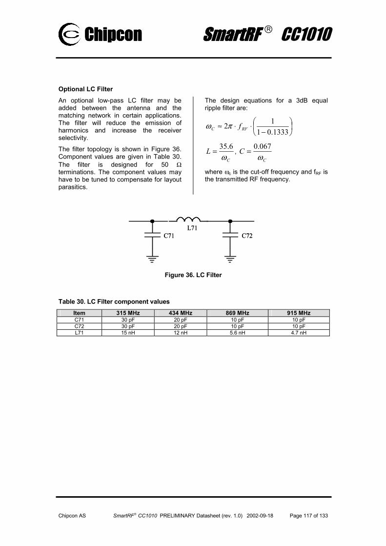
ChipconChipconChipconChipcon SmartRF SmartRF SmartRF SmartRF CC1010
Chipcon AS SmartRF CC1010 PRELIMINARY Datasheet (rev. 1.0) 2002-09-18 Page 117 of 133
Optional LC Filter An optional low-pass LC filter may be added between the antenna and the matching network in certain applications. The filter will reduce the emission of harmonics and increase the receiver selectivity.
The filter topology is shown in Figure 36. Component values are given in Table 30. The filter is designed for 50 Ω terminations. The component values may have to be tuned to compensate for layout parasitics.
The design equations for a 3dB equal ripple filter are:
−⋅⋅≈
1333.0112 RFC fπω
C
Lω
6.35= , C
Cω067.0=
where ωc is the cut-off frequency and fRF is the transmitted RF frequency.
L71C71 C72
L71C71 C72
Figure 36. LC Filter
Table 30. LC Filter component values
Item 315 MHz 434 MHz 869 MHz 915 MHz C71 30 pF 20 pF 10 pF 10 pF C72 30 pF 20 pF 10 pF 10 pF L71 15 nH 12 nH 5.6 nH 4.7 nH
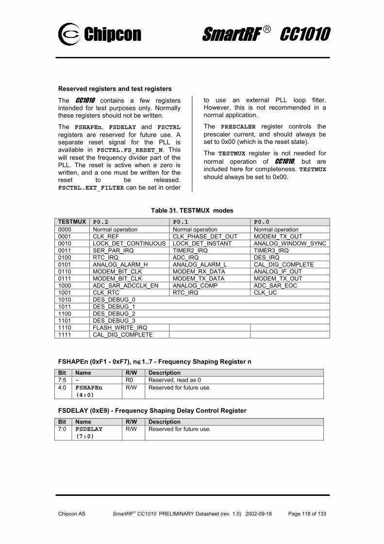
ChipconChipconChipconChipcon SmartRF SmartRF SmartRF SmartRF CC1010
Chipcon AS SmartRF CC1010 PRELIMINARY Datasheet (rev. 1.0) 2002-09-18 Page 118 of 133
Reserved registers and test registers
The CC1010 contains a few registers intended for test purposes only. Normally these registers should not be written.
The FSHAPEn, FSDELAY and FSCTRL registers are reserved for future use. A separate reset signal for the PLL is available in FSCTRL.FS_RESET_N. This will reset the frequency divider part of the PLL. The reset is active when a zero is written, and a one must be written for the reset to be released. FSCTRL.EXT_FILTER can be set in order
to use an external PLL loop filter. However, this is not recommended in a normal application.
The PRESCALER register controls the prescaler current, and should always be set to 0x00 (which is the reset state).
The TESTMUX register is not needed for normal operation of CC1010, but are included here for completeness. TESTMUX should always be set to 0x00.
Table 31. TESTMUX modes TESTMUX P0.2 P0.1 P0.00000 Normal operation Normal operation Normal operation 0001 CLK_REF CLK_PHASE_DET_OUT MODEM_TX_OUT 0010 LOCK_DET_CONTINUOUS LOCK_DET_INSTANT ANALOG_WINDOW_SYNC 0011 SER_PAR_IRQ TIMER2_IRQ TIMER3_IRQ 0100 RTC_IRQ ADC_IRQ DES_IRQ 0101 ANALOG_ALARM_H ANALOG_ALARM_L CAL_DIG_COMPLETE 0110 MODEM_BIT_CLK MODEM_RX_DATA ANALOG_IF_OUT 0111 MODEM_BIT_CLK MODEM_TX_DATA MODEM_TX_OUT 1000 ADC_SAR_ADCCLK_EN ANALOG_COMP ADC_SAR_EOC 1001 CLK_RTC RTC_IRQ CLK_UC 1010 DES_DEBUG_0 1011 DES_DEBUG_1 1100 DES_DEBUG_2 1101 DES_DEBUG_3 1110 FLASH_WRITE_IRQ 1111 CAL_DIG_COMPLETE
FSHAPEn (0xF1 - 0xF7), n∈∈∈∈1..7 - Frequency Shaping Register n Bit Name R/W Description 7:5 - R0 Reserved, read as 0 4:0 FSHAPEn
(4:0)R/W Reserved for future use.
FSDELAY (0xE9) - Frequency Shaping Delay Control Register Bit Name R/W Description 7:0 FSDELAY
(7:0)R/W Reserved for future use.

ChipconChipconChipconChipcon SmartRF SmartRF SmartRF SmartRF CC1010
Chipcon AS SmartRF CC1010 PRELIMINARY Datasheet (rev. 1.0) 2002-09-18 Page 119 of 133
FSCTRL (0xEC) - Frequency Synthesiser Control Register Bit Name R/W Description 7:5 - R0 Reserved, read as 0 4 EXT_FILTER R/W Setting for external loop filter (not recommended)
0 : Internal loop filter (recommended) 1 : External loop filter
3 DITHER1 R/W Reserved for future use. Write as 0.
2 DITHER0 R/W Reserved for future use. Write as 0.
1 SHAPE R/W Reserved for future use. Write as 0.
0 FS_RESET_N R/W Separate reset of frequency synthesiser 0 : Frequency synthesiser is reset 1 : Frequency synthesiser reset is released
PRESCALER (0xE6) - Prescaler Control Register Bit Name R/W Description 7 PRE_SWING
(1:0)R/W Prescaler swing. Fractions for PRE_CURRENT[1:0] = 00
00 : 1 * Nominal Swing 01 : 2/3 * Nominal Swing 10 : 7/3 * Nominal Swing 11 : 5/3 * Nominal Swing
5 PRE_CURRENT(1:0)
R/W Prescaler current scaling 00 : 1 * Nominal Current 01 : 2/3 * Nominal Current 10 : 1/2 * Nominal Current 11 : 2/5 * Nominal Current
3 IF_INPUT R/W 0 : Nominal setting 1 : AD2(RSSI/IF) pin is input to IF-strips
2 IF_FRONT R/W 0 : Nominal setting 1 : Output of IF_Front_amp is switched to the AD2(RSSI/IF) pin
1 - R/W Reserved for future use, always write 0
0 - R/W Reserved for future use, always write 0
TESTMUX (0xEF) - Test Multiplexer Control Register (for prototype testing) Bit Name R/W Description 7:4 - R0 Reserved, read as 0 3:0 TESTMUX
(3:0)R/W Select internal test signals to be output to P0(2:0). This function
is enabled when TESTMUX ≠ 0000. The port directions are still set by P0DIR.

ChipconChipconChipconChipcon SmartRF SmartRF SmartRF SmartRF CC1010
Chipcon AS SmartRF CC1010 PRELIMINARY Datasheet (rev. 1.0) 2002-09-18 Page 120 of 133
System Considerations and Guidelines
SRD regulations
International regulations and national laws regulate the use of radio receivers and transmitters. SRDs (Short Range Devices) for licence free operation are allowed to operate in the 433 and 868-870 MHz bands in most European countries. In the United States such devices operate in the 260–470 and 902-928 MHz bands. CC1010 is designed to meet the requirements for operation in all these bands. A summary of the most important aspects of these regulations can be found in Application Note AN001 SRD regulations for licence free transceiver operation, available from Chipcon’s web site.
Low cost systems
In systems where low cost is of great importance the CC1010 is the ideal choice. Very few external components keep the total cost at a minimum. The oscillator crystal can then be a low cost crystal with 50/25 ppm frequency tolerance at 433/868 MHz respectively.
Battery operated systems
In low power applications the RF Transceiver power down mode should be used when no communication takes place. Using receiver polling, that is, listening for transmissions for a few milliseconds at regular intervals, will also save a lot of battery power. The RSSI can be used as a first indication that a transmission is received. See page 84 for information on how effective power management can be implemented. Utilizing the Idle mode and Power down modes and clock modes of the MCU will also reduce the power consumption significantly. See page 31 for details.
Narrow-band systems
CC400 and CC900 are recommended for best performance in narrow-band applications. The phase noise of CC400 and CC900 is superior and for systems
with 25 kHz channel spacing or less. With strict requirements to ACP (Adjacent Channel Power), low phase noise is important.
The selectivity of CC1010 can be improved by using an external ceramic filter and demodulator at 10.7 MHz. Such ceramic filters are typically 180 or 280 kHz wide.
A unique feature in CC1010 is the very fine frequency resolution of < 250 Hz. This can be used to do the temperature compensation of the crystal if the temperature drift curve is known and a temperature sensor is included in the system. Even initial adjustment can be done using the frequency programmability. This eliminates the need for an expensive TCXO and trimming in some applications. In less demanding applications a crystal with low temperature drift and low ageing could be used without further compensation. A trimmer capacitor in the crystal oscillator circuit (in parallel with C171) could be used to set the initial frequency accurately. The fine frequency step programming cannot be used in RX mode if optimised frequency settings are required (see page 103).
High reliability systems
Using a SAW filter as a preselector between the antenna and the RF input will improve the communication reliability in harsh environments by reducing the probability of blocking. The receiver sensitivity and the output power will be reduced due to the filter insertion loss. By inserting the filter in the RX path only, together with an external RX/TX switch, only the receiver sensitivity is reduced, and output power is unaffected. Any general-purpose I/O pins can be configured to control an external LNA, RX/TX switch or power amplifier.
Frequency hopping spread spectrum systems
Due to the very fast frequency shift properties of the PLL, the CC1010 is very

ChipconChipconChipconChipcon SmartRF SmartRF SmartRF SmartRF CC1010
Chipcon AS SmartRF CC1010 PRELIMINARY Datasheet (rev. 1.0) 2002-09-18 Page 121 of 133
suitable for frequency hopping systems. Hop rates of 10-1000 hops/s are usually used depending on the bit rate and the amount of data to be sent during each transmission. The two frequency registers (FREQ_A and FREQ_B) are designed such that the ‘next’ frequency can be programmed while the ‘present’ frequency is used. The switching between the two frequencies is done through the RFMAIN.F_REG control bit. Frequency hopping improve the reliability and increase the security in a wireless link. The US ISM band at 902 – 928 MHz is very suitable for frequency hopping protocols.

ChipconChipconChipconChipcon SmartRF SmartRF SmartRF SmartRF CC1010
Chipcon AS SmartRF CC1010 PRELIMINARY Datasheet (rev. 1.0) 2002-09-18 Page 122 of 133
PCB Layout RecommendationsChipcon provide reference layouts that should be followed in order to achieve the best performance. The reference designs can be downloaded from the Chipcon website.
A four layer PCB is highly recommended. The top layer should be used for signal routing, and the open areas should be filled with metallisation connected to ground using several vias. The second layer of the PCB should be the “ground-plane”. Layer three is used for power supply and layer four for general routing and decoupling. A few components are also placed at the reverse side (VCO inductor and power filtering).
The ground pins should be connected to ground as close as possible to the package pin using individual vias for each
pin. The de-coupling capacitors should also be placed as close as possible to the supply pins and connected to the ground plane by separate vias.
The external components should be as small as possible and surface mount devices are required. The VCO inductor must be placed as close as possible to the chip and symmetrical with respect to the input pins. It is important to keep the coupling between the VCO inductor and the matching network very low in order to reduce LO leakage. Due to this the VCO inductor is placed at the reverse side of the PCB.
A development kit with a fully assembled PCB is available, and can be used as a guideline for layout.
Antenna Considerations
CC1010 can be used together with various types of antennas. The most common antennas for short-range devices are monopole, helical and loop antennas.
Monopole antennas are resonant antennas with a length corresponding to one quarter of the electrical wavelength (λ/4). They are very easy to design and can be implemented simply as a “piece of wire” or even integrated into the PCB.
Non-resonant monopole antennas shorter than λ/4 can also be used, but at the expense of range. In size and cost critical applications such an antenna may very well be integrated into the PCB.
Helical antennas can be thought of as a combination of a monopole and a loop antenna. They are a good compromise in size critical applications. But helical antennas tend to be more difficult to optimise than the simple monopole.
Loop antennas are easy to integrate into the PCB, but are less effective due to
difficult impedance matching because of their very low radiation resistance if they are made small.
For low power applications the λ/4-monopole antenna is recommended giving the best range and because of its simplicity.
The length of the λ/4-monopole antenna is given by:
L = 7125 / f
where f is in MHz, giving the length in cm. An antenna for 869 MHz should be 8.2 cm, and 16.4 cm for 434 MHz.
The antenna should be connected as close as possible to the IC. If the antenna is located away from the input pin the antenna should be matched to the feeding transmission line (50 Ω).
For a more thorough primer on antennas, please refer to Application Note AN003 SRD Antennas available from Chipcon’s web site.
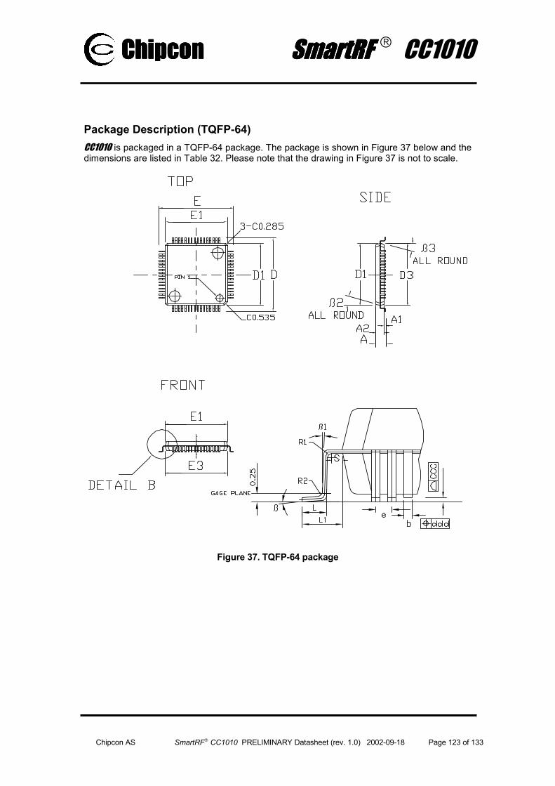
ChipconChipconChipconChipcon SmartRF SmartRF SmartRF SmartRF CC1010
Chipcon AS SmartRF CC1010 PRELIMINARY Datasheet (rev. 1.0) 2002-09-18 Page 123 of 133
Package Description (TQFP-64) CC1010 is packaged in a TQFP-64 package. The package is shown in Figure 37 below and the dimensions are listed in Table 32. Please note that the drawing in Figure 37 is not to scale.
Figure 37. TQFP-64 package
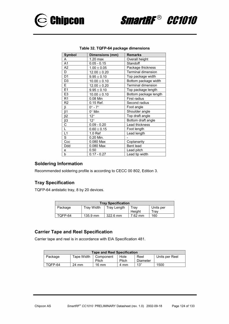
ChipconChipconChipconChipcon SmartRF SmartRF SmartRF SmartRF CC1010
Chipcon AS SmartRF CC1010 PRELIMINARY Datasheet (rev. 1.0) 2002-09-18 Page 124 of 133
Table 32. TQFP-64 package dimensions Symbol Dimensions (mm) Remarks A 1.20 max Overall height A1 0.05 - 0.15 Standoff A2 1.00 ± 0.05 Package thickness D 12.00 ± 0.20 Terminal dimension D1 9.95 ± 0.10 Top package width D3 10.00 ± 0.10 Bottom package width E 12.00 ± 0.20 Terminal dimension E1 9.95 ± 0.10 Top package length E3 10.00 ± 0.10 Bottom package length R1 0.08 Min First radius R2 0.15 Ref. Second radius β 0° - 7° Foot angle β1 0° Min Shoulder angle β2 12° Top draft angle β3 12° Bottom draft angle C 0.09 - 0.20 Lead thickness L 0.60 ± 0.15 Foot length L1 1.0 Ref Lead length S 0.20 Min. - Ccc 0.080 Max Coplanarity Ddd 0.080 Max Bent lead e 0.50 Lead pitch b 0.17 - 0.27 Lead tip width
Soldering Information Recommended soldering profile is according to CECC 00 802, Edition 3.
Tray Specification TQFP-64 antistatic tray, 8 by 20 devices.
Tray Specification
Package Tray Width Tray Length Tray Height
Units per Tray
TQFP-64 135.9 mm 322.6 mm 7.62 mm 160
Carrier Tape and Reel Specification Carrier tape and reel is in accordance with EIA Specification 481.
Tape and Reel Specification
Package Tape Width Component Pitch
Hole Pitch
Reel Diameter
Units per Reel
TQFP-64 24 mm 16 mm 4 mm 13” 1500
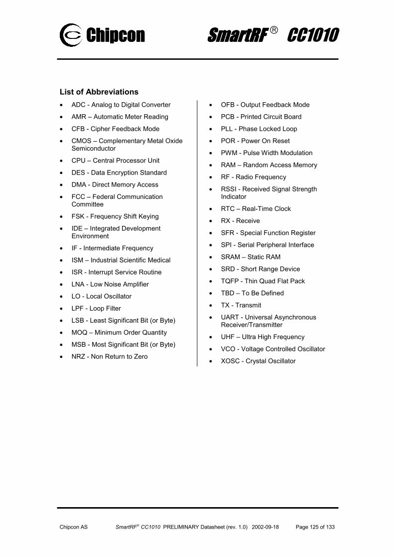
ChipconChipconChipconChipcon SmartRF SmartRF SmartRF SmartRF CC1010
Chipcon AS SmartRF CC1010 PRELIMINARY Datasheet (rev. 1.0) 2002-09-18 Page 125 of 133
List of Abbreviations • ADC - Analog to Digital Converter
• AMR – Automatic Meter Reading
• CFB - Cipher Feedback Mode
• CMOS – Complementary Metal Oxide Semiconductor
• CPU – Central Processor Unit
• DES - Data Encryption Standard
• DMA - Direct Memory Access
• FCC – Federal Communication Committee
• FSK - Frequency Shift Keying
• IDE – Integrated Development Environment
• IF - Intermediate Frequency
• ISM – Industrial Scientific Medical
• ISR - Interrupt Service Routine
• LNA - Low Noise Amplifier
• LO - Local Oscillator
• LPF - Loop Filter
• LSB - Least Significant Bit (or Byte)
• MOQ – Minimum Order Quantity
• MSB - Most Significant Bit (or Byte)
• NRZ - Non Return to Zero
• OFB - Output Feedback Mode
• PCB - Printed Circuit Board
• PLL - Phase Locked Loop
• POR - Power On Reset
• PWM - Pulse Width Modulation
• RAM – Random Access Memory
• RF - Radio Frequency
• RSSI - Received Signal Strength Indicator
• RTC – Real-Time Clock
• RX - Receive
• SFR - Special Function Register
• SPI - Serial Peripheral Interface
• SRAM – Static RAM
• SRD - Short Range Device
• TQFP - Thin Quad Flat Pack
• TBD – To Be Defined
• TX - Transmit
• UART - Universal Asynchronous Receiver/Transmitter
• UHF – Ultra High Frequency
• VCO - Voltage Controlled Oscillator
• XOSC - Crystal Oscillator

Chip
con
Chip
con
Chip
con
Chip
con
Sma
rtRF
Smar
tRF
Smar
tRF
Smar
tRF
CC1
010
Chi
pcon
AS
Sm
artR
F C
C10
10 P
REL
IMIN
ARY
Dat
ashe
et (r
ev. 1
.0)
200
2-09
-18
Page
126
of 1
33
SFR
Sum
mar
y A
sum
mar
y of
all
SFR
s w
ith a
ddre
ss, r
egis
ter n
ames
, bit
nam
es a
nd re
set v
alue
s ar
e sh
own
in T
able
33
belo
w.
Tabl
e 33
. SFR
Sum
mar
y (s
orte
d by
add
ress
) Ad
drN
ame
Bit
7 B
it 6
Bit
5 B
it 4
Bit
3 B
it 2
Bit
1 B
it 0
Res
et
Page
0x80
P0
P0
.7
P0.6
P0
.5
P0.4
P0
.3
P0.2
P0
.1
P0.0
00
0011
11
45
0x81
SP
SP
.7
SP.6
SP
.5
SP.4
SP
.3
SP.2
SP
.1
SP.0
00
0001
11
21
0x82
D
PL0
DPL
0.7
DPL
0.6
DPL
0.5
DPL
0.4
DPL
0.3
DPL
0.2
DPL
0.1
DPL
0.0
0000
0000
19
0x
83
DPH
0 D
PH0.
7 D
PH0.
6 D
PH0.
5 D
PH0.
4 D
PH0.
3 D
PH0.
2 D
PH0.
1 D
PH0.
0 00
0000
00
19
0x84
D
PL1
DPL
1.7
DPL
1.6
DPL
1.5
DPL
1.4
DPL
1.3
DPL
1.2
DPL
1.1
DPL
1.0
0000
0000
19
0x
85
DPH
1 D
PH1.
7 D
PH1.
6 D
PH1.
5 D
PH1.
4 D
PH1.
3 D
PH1.
2 D
PH1.
1 D
PH1.
0 00
0000
00
19
0x86
D
PS
- -
- -
- -
- SE
L 00
0000
00
20
0x87
PC
ON
SM
OD
0 -
- -
GF1
G
F0
STO
P ID
LE
0011
0000
32
0x
88
TCO
N
TF1
TR1
TF0
TR0
IE1
IT1
IE0
IT0
0000
0000
50
0x
89
TMO
D
GAT
E C
/T
M1
M0
GAT
E C
/T
M1
M0
0000
0000
49
0x
8A
TL0
TL0.
7 TL
0.6
TL0.
5 TL
0.4
TL0.
3 TL
0.2
TL0.
1 TL
0.0
0000
0000
48
0x
8B
TL1
TL1.
7 TL
1.6
TL1.
5 TL
1.4
TL1.
3 TL
1.2
TL1.
1 TL
1.0
0000
0000
48
0x
8C
TH0
TH0.
7 TH
0.6
TH0.
5 TH
0.4
TH0.
3 TH
0.2
TH0.
1 TH
0.0
0000
0000
48
0x
8D
TH1
TH1.
7 TH
1.6
TH1.
5 TH
1.4
TH1.
3 TH
1.2
TH1.
1 TH
1.0
0000
0000
48
0x
8E
CKC
ON
-
- T2
M
T1M
T0
M
MD
2 M
D1
MD
0 00
0000
01
51
0x8F
-
- -
- -
- -
- -
0000
0000
-
0x90
P1
P1
.7
P1.6
P1
.5
P1.4
P1
.3
P1.2
P1
.1
P1.0
11
1111
11
45
0x91
EX
IF
TF3
ADIF
TF
2 R
FIF
- -
- -
0000
1000
28
0x
92
MPA
GE
MPA
GE7
M
PAG
E6
MPA
GE5
M
PAG
E4
MPA
GE3
M
PAG
E2
MPA
GE1
M
PAG
E0
0000
0000
20
0x
93
ADC
ON
AD
_PD
-
ADC
M1
ADC
M0
ADC
REF
AD
CR
UN
AD
ADR
1 AD
ADR
0 10
0000
00
76
0x94
AD
DAT
L AD
DAT
7 AD
DAT
6 AD
DAT
5 AD
DAT
4 AD
DAT
3 AD
DAT
2 AD
DAT
1 AD
DAT
0 00
0000
00
76
0x95
AD
DAT
H
- -
- -
- -
ADD
AT9
ADD
AT8
0000
0000
76
0x
96
ADC
ON
2 AD
CIE
AD
CIF
AD
CD
IV5
ADC
DIV
4 AD
CD
IV3
ADC
DIV
2 AD
CD
IV1
ADC
DIV
0 00
0000
00
77
0x97
AD
TRH
AD
TRH
7 AD
TRH
6 AD
TRH
5 AD
TRH
4 AD
TRH
3 AD
TRH
2 AD
TRH
1 AD
TRH
0 00
0000
00
77
0x98
SC
ON
0 SM
0_0
SM1_
0 SM
2_0
REN
_0
TB8_
0 R
B8_0
TI
_0
RI_
0 00
0000
00
63
0x99
SB
UF0
SB
UF0
.7
SBU
F0.6
SB
UF0
.5
SBU
F0.4
SB
UF0
.3
SBU
F0.2
SB
UF0
.1
SBU
F0.0
00
0000
00
63
0x9A
.
- -
. .
. .
. .
0000
0000
-
0x9B
-
- -
- -
- -
- -
0000
0000
-

Chip
con
Chip
con
Chip
con
Chip
con
Sma
rtRF
Smar
tRF
Smar
tRF
Smar
tRF
CC1
010
Chi
pcon
AS
Sm
artR
F C
C10
10 P
REL
IMIN
ARY
Dat
ashe
et (r
ev. 1
.0)
200
2-09
-18
Page
127
of 1
33
Addr
Nam
e B
it 7
Bit
6 B
it 5
Bit
4 B
it 3
Bit
2 B
it 1
Bit
0 R
eset
Pa
ge
0x9C
-
- -
- -
- -
- -
0000
0000
-
0x9D
-
- -
- -
- -
- -
0000
0000
-
0x9E
-
- -
- -
- -
- -
0000
0000
-
0x9F
C
HVE
R
CH
IP_T
YPE5
C
HIP
_TYP
E4
CH
IP_T
YPE3
C
HIP
_TYP
E2
CH
IP_T
YPE1
C
HIP
_TYP
E0
CH
IP_R
EV1
CH
IP_R
EV0
0000
0000
42
0x
A0
P2
P2.7
P2
.6
P2.5
P2
.4
P2.3
P2
.2
P2.1
P2
.0
1111
1111
46
0x
A1
SPC
R
- -
SPE
DO
RD
C
POL
CPH
A SP
R1
SPR
0 00
0000
00
67
0xA2
SP
DR
SP
DR
7 SP
DR
6 SP
DR
5 SP
DR
4 SP
DR
3 SP
DR
2 SP
DR
1 SP
DR
0 00
0000
00
67
0xA3
SP
SR
- -
- -
- -
SPA
WC
OL
0000
0000
68
0x
A4
P0D
IR
- -
- -
P0D
IR3
P0D
IR2
P0D
IR1
P0D
IR0
0000
1111
46
0x
A5
P1D
IR
P1D
IR7
P1D
IR6
P1D
IR5
P1D
IR4
P1D
IR3
P1D
IR2
P1D
IR1
P1D
IR0
1111
1111
46
0x
A6
P2D
IR
P2D
IR7
P2D
IR6
P2D
IR5
P2D
IR4
P2D
IR3
P2D
IR2
P2D
IR1
P2D
IR0
1111
1111
47
0x
A7
P3D
IR
- -
P3D
IR5
P3D
IR4
P3D
IR3
P3D
IR2
P3D
IR1
P3D
IR0
0011
1111
47
0x
A8
IE
EA
- -
ES0
ET1
EX1
ET0
EX0
0000
0000
27
0x
A9
TCO
N2
- -
- -
TR3
M3
TR2
M2
0000
0000
54
0x
AA
T2PR
E T2
PRE7
T2
PRE6
T2
PRE5
T2
PRE4
T2
PRE3
T2
PRE2
T2
PRE1
T2
PRE0
00
0000
00
55
0xAB
T3
PRE
T3PR
E7
T3PR
E6
T3PR
E5
T3PR
E4
T3PR
E3
T3PR
E2
T3PR
E1
T3PR
E0
0000
0000
55
0x
AC
T2
T2.7
T2
.6
T2.5
T2
.4
T2.3
T2
.2
T2.1
T2
.0
0000
0000
55
0x
AD
T3
T3.7
T3
.6
T3.5
T3
.4
T3.3
T3
.2
T3.1
T3
.0
0000
0000
55
0x
AE
FLAD
R
FLAD
R7
FLAD
R6
FLAD
R5
FLAD
R4
FLAD
R3
FLAD
R2
FLAD
R1
FLAD
R0
0000
0000
39
0x
AF
FLC
ON
-
FLAS
H_L
P1
FLAS
H_L
P0
WR
FLAS
H
RM
ADR
3 R
MAD
R2
RM
ADR
1 R
MAD
R0
0000
0000
40
0x
B0
P3
P3.7
P3
.6
P3.5
P3
.4
P3.3
P3
.2
P3.1
P3
.0
1111
1111
46
0x
B1
- -
- -
- -
- -
- 00
0000
00
- 0x
B2
- -
- -
- -
- -
- 00
0000
00
- 0x
B3
- -
- -
- -
- -
- 00
0000
00
- 0x
B4
CR
PIN
I0
CR
PIN
I0.7
C
RPI
NI0
.6
CR
PIN
I0.5
C
RPI
NI0
.4
CR
PIN
I0.3
C
RPI
NI0
.2
CR
PIN
I0.1
C
RPI
NI0
.0
0000
0000
73
0x
B5
CR
PIN
I1
CR
PIN
I1.7
C
RPI
NI1
.6
CR
PIN
I1.5
C
RPI
NI1
.4
CR
PIN
I1.3
C
RPI
NI1
.2
CR
PIN
I1.1
C
RPI
NI1
.0
0000
0000
73
0x
B6
CR
PIN
I2
CR
PIN
I2.7
C
RPI
NI2
.6
CR
PIN
I2.5
C
RPI
NI2
.4
CR
PIN
I2.3
C
RPI
NI2
.2
CR
PIN
I2.1
C
RPI
NI2
.0
0000
0000
73
0x
B7
CR
PIN
I3
CR
PIN
I3.7
C
RPI
NI3
.6
CR
PIN
I3.5
C
RPI
NI3
.4
CR
PIN
I3.3
C
RPI
NI3
.2
CR
PIN
I3.1
C
RPI
NI3
.0
0000
0000
73
0x
B8
IP
- -
- PS
0 PT
1 PX
1 PT
0 PX
0 10
0000
00
29
0xB9
R
DAT
A R
DAT
A7
RD
ATA6
R
DAT
A5
RD
ATA4
R
DAT
A3
RD
ATA2
R
DAT
A1
RD
ATA0
00
0000
00
42
0xBA
R
ADR
L R
ADR
15
RAD
R14
R
ADR
13
RAD
R12
R
ADR
11
RAD
R10
R
ADR
9 R
ADR
8 00
0000
00
42
0xBB
R
ADR
H
RAD
R7
RAD
R6
RAD
R5
RAD
R4
RAD
R3
RAD
R2
RAD
R1
RAD
R0
0000
0000
42
0x
BC
CR
PIN
I4
CR
PIN
I4.7
C
RPI
NI4
.6
CR
PIN
I4.5
C
RPI
NI4
.4
CR
PIN
I4.3
C
RPI
NI4
.2
CR
PIN
I4.1
C
RPI
NI4
.0
0000
0000
73
0x
BD
CR
PIN
I5
CR
PIN
I5.7
C
RPI
NI5
.6
CR
PIN
I5.5
C
RPI
NI5
.4
CR
PIN
I5.3
C
RPI
NI5
.2
CR
PIN
I5.1
C
RPI
NI5
.0
0000
0000
73
0x
BE
CR
PIN
I6
CR
PIN
I6.7
C
RPI
NI6
.6
CR
PIN
I6.5
C
RPI
NI6
.4
CR
PIN
I6.3
C
RPI
NI6
.2
CR
PIN
I6.1
C
RPI
NI6
.0
0000
0000
73
0x
BF
CR
PIN
I7
CR
PIN
I7.7
C
RPI
NI7
.6
CR
PIN
I7.5
C
RPI
NI7
.4
CR
PIN
I7.3
C
RPI
NI7
.2
CR
PIN
I7.1
C
RPI
NI7
.0
0000
0000
73
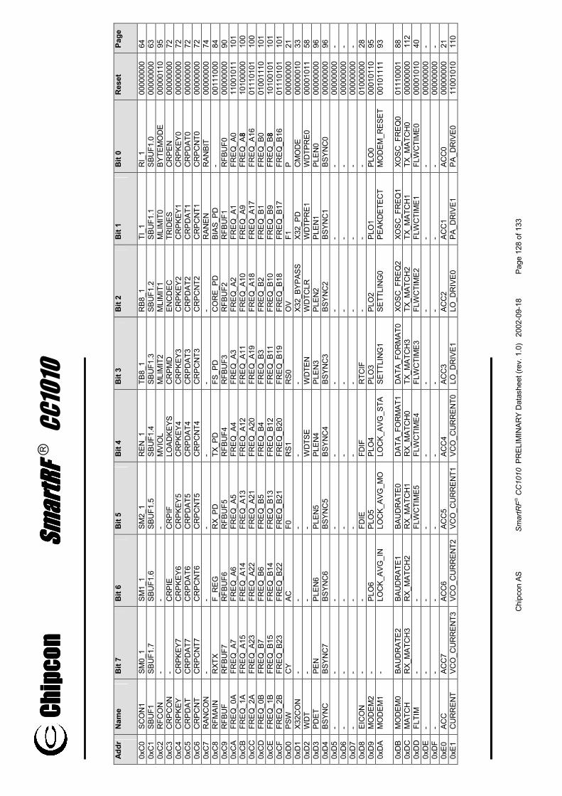
Chip
con
Chip
con
Chip
con
Chip
con
Sma
rtRF
Smar
tRF
Smar
tRF
Smar
tRF
CC1
010
Chi
pcon
AS
Sm
artR
F C
C10
10 P
REL
IMIN
ARY
Dat
ashe
et (r
ev. 1
.0)
200
2-09
-18
Page
128
of 1
33
Addr
Nam
e B
it 7
Bit
6 B
it 5
Bit
4 B
it 3
Bit
2 B
it 1
Bit
0 R
eset
Pa
ge
0xC
0 SC
ON
1 SM
0_1
SM1_
1 SM
2_1
REN
_1
TB8_
1 R
B8_1
TI
_1
RI_
1 00
0000
00
64
0xC
1 SB
UF1
SB
UF1
.7
SBU
F1.6
SB
UF1
.5
SBU
F1.4
SB
UF1
.3
SBU
F1.2
SB
UF1
.1
SBU
F1.0
00
0000
00
63
0xC
2 R
FCO
N
- -
- M
VIO
L M
LIM
IT2
MLI
MIT
1 M
LIM
IT0
BYTE
MO
DE
0000
0110
95
0x
C3
CR
PCO
N
- C
RPI
E C
RPI
F LO
ADKE
YS
CR
PMD
EN
CD
EC
TRID
ES
CR
PEN
00
0000
00
72
0xC
4 C
RPK
EY
CR
PKEY
7 C
RPK
EY6
CR
PKEY
5 C
RPK
EY4
CR
PKEY
3 C
RPK
EY2
CR
PKEY
1 C
RPK
EY0
0000
0000
72
0x
C5
CR
PDAT
C
RPD
AT7
CR
PDAT
6 C
RPD
AT5
CR
PDAT
4 C
RPD
AT3
CR
PDAT
2 C
RPD
AT1
CR
PDAT
0 00
0000
00
72
0xC
6 C
RPC
NT
CR
PCN
T7
CR
PCN
T6
CR
PCN
T5
CR
PCN
T4
CR
PCN
T3
CR
PCN
T2
CR
PCN
T1
CR
PCN
T0
0000
0000
72
0x
C7
RAN
CO
N
- -
- -
- -
RAN
EN
RAN
BIT
0000
0000
74
0x
C8
RFM
AIN
R
XTX
F_R
EG
RX_
PD
TX_P
D
FS_P
D
CO
RE_
PD
BIAS
_PD
-
0011
1000
84
0x
C9
RFB
UF
RFB
UF7
R
FBU
F6
RFB
UF5
R
FBU
F4
RFB
UF3
R
FBU
F2
RFB
UF1
R
FBU
F0
0000
0000
90
0x
CA
FREQ
_0A
FREQ
_A7
FREQ
_A6
FREQ
_A5
FREQ
_A4
FREQ
_A3
FREQ
_A2
FREQ
_A1
FREQ
_A0
1100
1011
10
1 0x
CB
FREQ
_1A
FREQ
_A15
FR
EQ_A
14
FREQ
_A13
FR
EQ_A
12
FREQ
_A11
FR
EQ_A
10
FREQ
_A9
FREQ
_A8
1010
0000
10
0 0x
CC
FR
EQ_2
A FR
EQ_A
23
FREQ
_A22
FR
EQ_A
21
FREQ
_A20
FR
EQ_A
19
FREQ
_A18
FR
EQ_A
17
FREQ
_A16
01
1101
01
100
0xC
D
FREQ
_0B
FREQ
_B7
FREQ
_B6
FREQ
_B5
FREQ
_B4
FREQ
_B3
FREQ
_B2
FREQ
_B1
FREQ
_B0
0100
1110
10
1 0x
CE
FREQ
_1B
FREQ
_B15
FR
EQ_B
14
FREQ
_B13
FR
EQ_B
12
FREQ
_B11
FR
EQ_B
10
FREQ
_B9
FREQ
_B8
1010
0101
10
1 0x
CF
FREQ
_2B
FREQ
_B23
FR
EQ_B
22
FREQ
_B21
FR
EQ_B
20
FREQ
_B19
FR
EQ_B
18
FREQ
_B17
FR
EQ_B
16
0111
0101
10
1 0x
D0
PSW
C
Y AC
F0
R
S1
RS0
O
V F1
P
0000
0000
21
0x
D1
X32C
ON
-
- -
- -
X32_
BYPA
SS
X32_
PD
CM
OD
E 00
0000
10
33
0xD
2 W
DT
- -
- W
DTS
E W
DTE
N
WD
TCLR
W
DTP
RE1
W
DTP
RE0
00
0010
11
58
0xD
3 PD
ET
PEN
PL
EN6
PLEN
5 PL
EN4
PLEN
3 PL
EN2
PLEN
1 PL
EN0
0000
0000
96
0x
D4
BSYN
C
BSYN
C7
BSYN
C6
BSYN
C5
BSYN
C4
BSYN
C3
BSYN
C2
BSYN
C1
BSYN
C0
0000
0000
96
0x
D5
- -
- -
- -
- -
- 00
0000
00
- 0x
D6
- -
- -
- -
- -
- 00
0000
00
- 0x
D7
- -
- -
- -
- -
- 00
0000
00
- 0x
D8
EIC
ON
-
- FD
IE
FDIF
R
TCIF
-
- -
0100
0000
28
0x
D9
MO
DEM
2 -
PLO
6 PL
O5
PLO
4 PL
O3
PLO
2 PL
O1
PLO
0 00
0101
10
95
0xD
A M
OD
EM1
- LO
CK_
AVG
_IN
LO
CK_
AVG
_MO
LOC
K_AV
G_S
TASE
TTLI
NG
1 SE
TTLI
NG
0 PE
AKD
ETEC
T M
OD
EM_R
ESET
0010
1111
93
0xD
B M
OD
EM0
BAU
DR
ATE2
BA
UD
RAT
E1
BAU
DR
ATE0
D
ATA_
FOR
MAT
1 D
ATA_
FOR
MAT
0 XO
SC_F
REQ
2 XO
SC_F
REQ
1 XO
SC_F
REQ
0 01
1100
01
88
0xD
C
MAT
CH
R
X_M
ATC
H3
RX_
MAT
CH
2 R
X_M
ATC
H1
RX_
MAT
CH
0 TX
_MAT
CH
3 TX
_MAT
CH
2 TX
_MAT
CH
1 TX
_MAT
CH
0 00
0000
00
112
0xD
D
FLTI
M
- -
FLW
CTI
ME5
FL
WC
TIM
E4
FLW
CTI
ME3
FL
WC
TIM
E2
FLW
CTI
ME1
FL
WC
TIM
E0
0000
1010
40
0x
DE
- -
- -
- -
- -
- 00
0000
00
- 0x
DF
- -
- -
- -
- -
- 00
0000
00
- 0x
E0
ACC
AC
C7
ACC
6 AC
C5
ACC
4 AC
C3
ACC
2 AC
C1
ACC
0 00
0000
00
21
0xE1
C
UR
REN
T VC
O_C
UR
REN
T3
VCO
_CU
RR
ENT2
VC
O_C
UR
REN
T1
VCO
_CU
RR
ENT0
LO
_DR
IVE1
LO
_DR
IVE0
PA
_DR
IVE1
PA
_DR
IVE0
11
0010
10
110

Chip
con
Chip
con
Chip
con
Chip
con
Sma
rtRF
Smar
tRF
Smar
tRF
Smar
tRF
CC1
010
Chi
pcon
AS
Sm
artR
F C
C10
10 P
REL
IMIN
ARY
Dat
ashe
et (r
ev. 1
.0)
200
2-09
-18
Page
129
of 1
33
Addr
Nam
e B
it 7
Bit
6 B
it 5
Bit
4 B
it 3
Bit
2 B
it 1
Bit
0 R
eset
Pa
ge
0xE2
PA
_PO
W
PA_H
IGH
POW
ERPA
_HIG
HPO
WER
PA_H
IGH
POW
ERPA
_HIG
HPO
WER
PA_L
OW
POW
ERPA
_LO
WPO
WER
PA_L
OW
POW
ERPA
_LO
WPO
WER
0000
1111
11
3
0xE3
PL
L R
EFD
IV4
REF
DIV
3 R
EFD
IV2
REF
DIV
1 R
EFD
IV0
ALAR
M_D
ISAB
LAL
ARM
_H
ALAR
M_L
00
0100
xx
101
0xE4
LO
CK
- -
- -
PLL_
LOC
K_
ACC
UR
ACY
PLL_
LOC
K_
LEN
GTH
LO
CK_
INST
ANT
LOC
K_
CO
NTI
NU
OU
S 00
0000
xx
102
0xE5
C
AL
CAL
_STA
RT
CAL
_DU
AL
CAL
_WAI
T C
AL_C
UR
REN
T C
AL_C
OM
PLET
E C
AL_I
TER
ATE2
C
AL_I
TER
ATE1
C
AL_I
TER
ATE0
00
0001
01
106
0xE6
PR
ESC
ALE
PRE_
SWIN
G1
PRE_
SWIN
G0
PRE_
CU
RR
ENT1
PR
E_C
UR
REN
T0
IF_I
NPU
T IF
_FR
ON
T PR
ESC
ALE.
1 PR
ESC
ALE.
0 00
0000
00
118
0xE7
R
ESER
VED
R
ESER
VED
.7
RES
ERVE
D.6
R
ESER
VED
.5
RES
ERVE
D.4
R
ESER
VED
.3
RES
ERVE
D.2
R
ESER
VED
.1
RES
ERVE
D.0
00
0000
00
42
0xE8
EI
E -
- -
RTC
IE
ET3
ADIE
ET
2 R
FIE
1110
0000
27
0x
E9
FSD
ELAY
FS
DEL
AY7
FSD
ELAY
6 FS
DEL
AY5
FSD
ELAY
4 FS
DEL
AY3
FSD
ELAY
2 FS
DEL
AY1
FSD
ELAY
0 00
1011
11
118
0xEA
FS
EP0
FSEP
7 FS
EP6
FSEP
5 FS
EP4
FSEP
3 FS
EP2
FSEP
1 FS
EP0
0101
1001
10
1 0x
EB
FSEP
1 -
- -
- -
FSEP
10
FSEP
9 FS
EP8
0000
0000
10
1 0x
EC
FSC
TRL
- -
- EX
T_FI
LTER
D
ITH
ER1
DIT
HER
0 SH
APE
FS_R
ESET
_N
0000
0001
11
9 0x
ED
RTC
ON
R
TEN
R
T6
RT5
R
T4
RT3
R
T2
RT1
R
T0
0000
0000
61
0x
EE
FREN
D
- -
LNA_
BUF_
CU
R
LNA_
CU
RR
ENT1
LN
A_C
UR
REN
T0
IF_E
XTER
NAL
R
SSI
- 00
0000
00
111
0xEF
TE
STM
UX
- -
- -
TEST
SEL3
TE
STSE
L2
TEST
SEL1
TE
STSE
L0
0000
0000
11
9 0x
F0
B B.
7 B.
6 B.
5 B.
4 B.
3 B.
2 B.
1 B.
0 00
0000
00
21
0xF1
FS
HAP
E7
FSH
APE7
.7
FSH
APE7
.6
FSH
APE7
.5
FSH
APE7
.4
FSH
APE7
.3
FSH
APE7
.2
FSH
APE7
.1
FSH
APE7
.0
0001
1100
11
8 0x
F2
FSH
APE6
FS
HAP
E6.7
FS
HAP
E6.6
FS
HAP
E6.5
FS
HAP
E6.4
FS
HAP
E6.3
FS
HAP
E6.2
FS
HAP
E6.1
FS
HAP
E6.0
00
0101
10
118
0xF3
FS
HAP
E5
FSH
APE5
.7
FSH
APE5
.6
FSH
APE5
.5
FSH
APE5
.4
FSH
APE5
.3
FSH
APE5
.2
FSH
APE5
.1
FSH
APE5
.0
0001
0000
11
8 0x
F4
FSH
APE4
FS
HAP
E4.7
FS
HAP
E4.6
FS
HAP
E4.5
FS
HAP
E4.4
FS
HAP
E4.3
FS
HAP
E4.2
FS
HAP
E4.1
FS
HAP
E4.0
00
0010
10
118
0xF5
FS
HAP
E3
FSH
APE3
.7
FSH
APE3
.6
FSH
APE3
.5
FSH
APE3
.4
FSH
APE3
.3
FSH
APE3
.2
FSH
APE3
.1
FSH
APE3
.0
0000
0110
11
8 0x
F6
FSH
APE2
FS
HAP
E2.7
FS
HAP
E2.6
FS
HAP
E2.5
FS
HAP
E2.4
FS
HAP
E2.3
FS
HAP
E2.2
FS
HAP
E2.1
FS
HAP
E2.0
00
0000
11
118
0xF7
FS
HAP
E1
FSH
APE1
.7
FSH
APE1
.6
FSH
APE1
.5
FSH
APE1
.4
FSH
APE1
.3
FSH
APE1
.2
FSH
APE1
.1
FSH
APE1
.0
0000
0001
11
8 0x
F8
EIP
- -
- PR
TC
PT3
PAD
PT
2 PR
F 11
1000
00
29
0xF9
TE
ST0
- -
- -
VCO
_AR
RAY
3 VC
O_A
RR
AY2
VCO
_AR
RAY
1 VC
O_A
RR
AY0
0000
xxxx
10
7 0x
FA
TEST
1 -
- -
- C
AL_D
AC3
CAL
_DAC
2 C
AL_D
AC1
CAL
_DAC
0 00
00xx
xx
107
0xFB
TE
ST2
- -
- C
HP_
CU
RR
ENT4
C
HP_
CU
RR
ENT3
C
HP_
CU
RR
ENT2
C
HP_
CU
RR
ENT1
C
HP_
CU
RR
ENT0
00
0xxx
xx
107
0xFC
TE
ST3
- -
- BR
EAK_
LOO
P C
AL_D
AC_
OPE
N3
CAL
_DAC
_ O
PEN
2 C
AL_D
AC_
OPE
N1
CAL
_DAC
_ O
PEN
0 00
0001
00
107
0xFD
TE
ST4
- -
L2KI
O0.
5 L2
KIO
0.4
L2KI
O0.
3 L2
KIO
0.2
L2KI
O0.
1 L2
KIO
0.0
0010
0101
10
7 0x
FE
TEST
5 -
- C
HP_
DIS
ABLE
VC
O_O
VER
RID
E VC
O_A
O3
VCO
_AO
2 VC
O_A
O1
VCO
_AO
0 00
0010
00
107
0xFF
TE
ST6
LOO
PFIL
TER
_ TP
1 LO
OPF
ILTE
R_
TP2
CH
P_O
VER
RID
E C
HP_
CO
4 C
HP_
CO
3 C
HP_
CO
2 C
HP_
CO
1 C
HP_
CO
0 00
0100
00
106

ChipconChipconChipconChipcon SmartRF SmartRF SmartRF SmartRF CC1010
Chipcon AS SmartRF CC1010 PRELIMINARY Datasheet (rev. 1.0) 2002-09-18 Page 130 of 133
Alphabetic Register Index ACC (0xE0) - Accumulator Register ........................................................................................ 21
ADCON (0x93) - ADC Control Register................................................................................... 76
ADCON 2(0x96) - ADC Control Register 2.............................................................................. 77
ADDATH (0x95) - ADC Data Register, High Bits..................................................................... 76
ADDATL (0x94) - ADC Data Register, Low Byte..................................................................... 76
ADTRH (0x97) - ADC Threshold Register ............................................................................... 77
B (0xF0) - B Register ............................................................................................................... 21
BSYNC (0xD4) - Byte Synchronisation Register ..................................................................... 96
CAL (0xE5) - PLL Calibration Control Register ..................................................................... 106
CHVER (0x9F) - Chip Version / Revision Register.................................................................. 42
CKCON (0x8E) - Timer Clock rate Control Register................................................................ 51
CRPCNT (0xC6) – Encryption / Decryption Counter ............................................................... 72
CRPCON (0xC3) - Encryption / Decryption Control Register.................................................. 72
CRPDAT (0xC5) - Encryption / Decryption Data Location Register ........................................ 72
CRPINIn, n∈0..7 (0xB4-0xB7, 0xBC-0xBF) - DES Initialisation Vector ................................ 73
CRPKEY (0xC4) - Encryption / Decryption Key Location Register ......................................... 72
CURRENT (0xE1) - RF Current Control Register.................................................................. 110
DPH0 (0x83) - Data Pointer 0, high byte ................................................................................. 19
DPH1 (0x85) - Data Pointer 1, high byte ................................................................................. 19
DPL0 (0x82) - Data Pointer 0, low byte ................................................................................... 19
DPL1 (0x84) - Data Pointer 1, low byte ................................................................................... 19
DPS (0x86) - Data Pointer Select ............................................................................................ 20
EICON (0xD8) - Extended Interrupt Control ............................................................................ 28
EIE (0xE8) - Extended Interrupt Enable Register .................................................................... 27
EIP (0xF8) - Extended Interrupt Priority Register .................................................................... 29
EXIF (0x91) - Extended Interrupt Flag..................................................................................... 28
FLADR (0xAE) - Flash Write Address Register ....................................................................... 39
FLCON (0xAF) - Flash Write Control Register ........................................................................ 40
FLTIM (0xDD) - Flash Write Timing Register .......................................................................... 40
FREND (0xEE) - Front End Control Register ........................................................................ 111
FREQ_0A (0xCA) – Frequency A, Control Register 0........................................................... 101
FREQ_0B (0xCD) - Frequency B, Control Register 0 ........................................................... 101
FREQ_1A (0xCB) – Frequency A, Control Register 1........................................................... 100
FREQ_1B (0xCE) - Frequency B, Control Register 1............................................................ 101
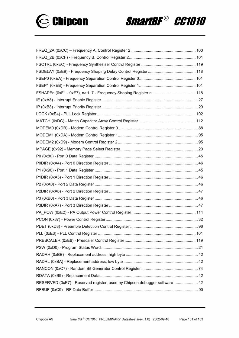
ChipconChipconChipconChipcon SmartRF SmartRF SmartRF SmartRF CC1010
Chipcon AS SmartRF CC1010 PRELIMINARY Datasheet (rev. 1.0) 2002-09-18 Page 131 of 133
FREQ_2A (0xCC) – Frequency A, Control Register 2 .......................................................... 100
FREQ_2B (0xCF) - Frequency B, Control Register 2............................................................ 101
FSCTRL (0xEC) - Frequency Synthesiser Control Register ................................................. 119
FSDELAY (0xE9) - Frequency Shaping Delay Control Register ........................................... 118
FSEP0 (0xEA) - Frequency Separation Control Register 0................................................... 101
FSEP1 (0xEB) - Frequency Separation Control Register 1................................................... 101
FSHAPEn (0xF1 - 0xF7), n∈1..7 - Frequency Shaping Register n ....................................... 118
IE (0xA8) - Interrupt Enable Register....................................................................................... 27
IP (0xB8) - Interrupt Priority Register....................................................................................... 29
LOCK (0xE4) - PLL Lock Register ......................................................................................... 102
MATCH (0xDC) - Match Capacitor Array Control Register ................................................... 112
MODEM0 (0xDB) - Modem Control Register 0........................................................................ 88
MODEM1 (0xDA) - Modem Control Register 1........................................................................ 95
MODEM2 (0xD9) - Modem Control Register 2 ........................................................................ 95
MPAGE (0x92) - Memory Page Select Register...................................................................... 20
P0 (0x80) - Port 0 Data Register ............................................................................................. 45
P0DIR (0xA4) - Port 0 Direction Register ................................................................................ 46
P1 (0x90) - Port 1 Data Register ............................................................................................. 45
P1DIR (0xA5) - Port 1 Direction Register ................................................................................ 46
P2 (0xA0) - Port 2 Data Register ............................................................................................. 46
P2DIR (0xA6) - Port 2 Direction Register ................................................................................ 47
P3 (0xB0) - Port 3 Data Register ............................................................................................. 46
P3DIR (0xA7) - Port 3 Direction Register ................................................................................ 47
PA_POW (0xE2) - PA Output Power Control Register.......................................................... 114
PCON (0x87) - Power Control Register................................................................................... 32
PDET (0xD3) - Preamble Detection Control Register ............................................................. 96
PLL (0xE3) - PLL Control Register ........................................................................................ 101
PRESCALER (0xE6) - Prescaler Control Register ................................................................ 119
PSW (0xD0) - Program Status Word ....................................................................................... 21
RADRH (0xBB) - Replacement address, high byte ................................................................. 42
RADRL (0xBA) - Replacement address, low byte ................................................................... 42
RANCON (0xC7) - Random Bit Generator Control Register ................................................... 74
RDATA (0xB9) - Replacement Data ........................................................................................ 42
RESERVED (0xE7) - Reserved register, used by Chipcon debugger software...................... 42
RFBUF (0xC9) - RF Data Buffer .............................................................................................. 90

ChipconChipconChipconChipcon SmartRF SmartRF SmartRF SmartRF CC1010
Chipcon AS SmartRF CC1010 PRELIMINARY Datasheet (rev. 1.0) 2002-09-18 Page 132 of 133
RFCON (0xC2) - RF Control Register ..................................................................................... 95
RFMAIN (0xC8) - RF Main Control Register ........................................................................... 84
RTCON (0xED) - Realtime Clock Control Register ................................................................. 61
SBUF0 (0x99) - Serial Port 0, data buffer................................................................................ 63
SBUF1 (0xC1) – Serial Port 1, data buffer .............................................................................. 63
SCON0 (0x98) - Serial Port 0 Control Register ....................................................................... 63
SCON1 (0xC0) - Serial Port 1 Control Register....................................................................... 64
SP (0x81) - Stack Pointer ........................................................................................................ 21
SPCR (0xA1) - SPI Control Register ....................................................................................... 67
SPDR (0xA2) - SPI Data Register ........................................................................................... 67
SPSR (0xA3) - SPI Status Register......................................................................................... 68
T2 (0xAC) - Timer 2 Low byte counter value ........................................................................... 55
T2PRE (0xAA) - Timer 2 Prescaler Control ............................................................................. 55
T3 (0xAD) - Timer 3 Low byte counter value ........................................................................... 55
T3PRE (0xAB) - Timer 3 Prescaler Control ............................................................................. 55
TCON (0x88) - Timer / Counter 0 and 1 control register ......................................................... 50
TCON2 (0xA9) - Timer Control register 2 ................................................................................ 54
TEST0 (0xF9) – PLL Test Register 0 .................................................................................... 107
TEST1 (0xFA) – PLL Test Register 1 .................................................................................... 107
TEST2 (0xFB) – PLL Test Register 2 .................................................................................... 107
TEST3 (0xFC) – PLL Test Register 3.................................................................................... 107
TEST4 (0xFD) – PLL Test Register 4.................................................................................... 107
TEST5 (0xFE) – PLL Test Register 5 .................................................................................... 107
TEST6 (0xFF) – PLL Test Register 6 .................................................................................... 106
TESTMUX (0xEF) - Test Multiplexer Control Register (for prototype testing)....................... 119
TH0 (0x8C) - Timer / Counter 0 High byte counter value ........................................................ 48
TH1 (0x8D) - Timer / Counter 1 High byte counter value ........................................................ 48
TL0 (0x8A) - Timer / Counter 0 Low byte counter value.......................................................... 48
TL1 (0x8B) - Timer / Counter 1 Low byte counter value.......................................................... 48
TMOD (0x89) - Timer / Counter 0 and 1 Mode register........................................................... 49
WDT (0xD2) - Watchdog Timer Control Register .................................................................... 58
X32CON (0xD1) - 32.768 kHz Crystal Oscillator Control Register.......................................... 33

ChipconChipconChipconChipcon SmartRF SmartRF SmartRF SmartRF CC1010
Chipcon AS SmartRF CC1010 PRELIMINARY Datasheet (rev. 1.0) 2002-09-18 Page 133 of 133
Ordering Information Ordering part number Description MOQ CC1010 Single Chip RF Transceiver with MCU 160 (tray) CC1010/T&R Single Chip RF Transceiver with MCU 1500 (tape and reel) CC1010DK-433 CC1010 Development Kit, 433 MHz 1 CC1010DK-868 CC1010 Development Kit, 868/915
MHz 1
CC1010SK CC1010 Sample Kit (5 pcs) 1 MOQ = Minimum Order Quantity
Contact information
Chipcon AS Gaustadalléen 21 N-0349 Oslo NORWAY Telephone : (+47) 22 95 85 44 Fax : (+47) 22 95 85 46 E-mail : [email protected] (information about RF-IC products) [email protected] (support on our standard products) Web site : http://www.chipcon.com General Information
Chipcon AS believes the information contained herein is correct and accurate at the time of this printing. However, Chipcon AS reserves the right to make changes to this product without notice. Chipcon AS does not assume any responsibility for the use of the described product. The latest updates are available at the Chipcon website or by contacting Chipcon directly. SmartRF is a registered trademark of Chipcon AS. SmartRF is Chipcon's RF technology platform with RF library cells, modules and design expertise. Based on SmartRF technology Chipcon develops standard component RF circuits as well as full custom ASICs based on customer requirements and this technology.
All other trademarks, registered trademarks and product names are the sole property of their respective owners.
Disclaimer This Chipcon product contains Flash memory code protection. However, Chipcon does not guarantee the security of this protection. Chipcon customers using or selling these products with program code do so at their own risk and agree to fully indemnify Chipcon AS for any damages resulting from the use or sale of such products.
Chipcon believes that the Flash memory protection used in this product is one of the most secure of its kind in the market today when used in the intended manner and under normal conditions. However, there are dishonest and possibly illegal methods to breach the code protection feature. All of these methods, to our knowledge, require using the product in a manner outside the operating specifications. The person doing so may be engaged in theft of intellectual property. Neither Chipcon nor any other semiconductor manufacturer can guarantee the security of their code protection. Code protection does not mean that we are guaranteeing the product as “unbreakable”.
This Chipcon product contains hardware DES encryption. Chipcon does not guarantee the security of the key protection or the security of the encryption scheme. Chipcon customers using or selling products with DES do so at their own risk and agree to fully indemnify Chipcon AS for any damages resulting from the use or sale of such products.
Life Support Policy This Chipcon product is not designed for use in life support appliances, devices, or other systems where malfunction can reasonably be expected to result in significant personal injury to the user, or as a critical component in any life support device or system whose failure to perform can be reasonably expected to cause the failure of the life support device or system, or to affect its safety or effectiveness. Chipcon AS customers using or selling these products for use in such applications do so at their own risk and agree to fully indemnify Chipcon AS for any damages resulting from any improper use or sale.
Related Documents