Atomic Layer Deposition of Noble Metals and Their Oxides Jani Ha ̈ ma ̈ lä inen,* Mikko Ritala,* and Markku Leskela ̈ * Laboratory of Inorganic Chemistry, Department of Chemistry, University of Helsinki, P.O. Box 55, FI-00014 Helsinki, Finland ABSTRACT: Atomic layer deposition (ALD) is an attractive method to deposit thin films for advanced technological applications such as microelectronics and nanotechnology. One material group in ALD that has matured in 10 years and proven to be of wide technological importance is noble metals. In this paper, thermal ALD of noble metals and their oxides is reviewed. Noble metal films are mostly grown using O 2 as the nonmetal precursor in a combustion-type chemistry. Alternatively, lower growth temperatures can be reached via noble metal oxide growth with consecutive reactions with ozone and H 2 . The use of true reducing chemistry (i.e., H 2 ) is typical only for ALD of palladium at low temperatures. On the other hand, ALD of noble metal oxides has been limited with reactants such as ozone and O 2 gas. In this review, reaction mechanisms in various types of processes are discussed and issues in nucleation are addressed. Deposition temperatures, film growth rates, and purities as well as evaporation temperatures used for noble metal precursors are tabulated for comparison. KEYWORDS: atomic layer deposition, ALD, noble metal, noble metal oxide, ruthenium, rhodium, palladium, osmium, iridium, platinum, thin film 1. INTRODUCTION Noble Metals and Their Oxides. Noble metals consist of metallic elements that have outstanding resistance to oxidation even at high temperatures. Noble metals also resist chemical action, do not corrode, and are not easily attacked by acids. According to the generally accepted definition, the noble metals include ruthenium, osmium, rhodium, iridium, palladium, platinum, silver, and gold. The noble metals are good conductors, but they are even better known as catalysts that readily accelerate or control the rate of many oxidation, reduction, and hydrogenation reactions. Although the noble metals resist oxidation, they can still be oxidized, and relatively stable noble metal oxides are formed. Selected properties of the noble metal oxides are summarized in Table 1. However, the noble metal oxides may decompose quite easily upon heating. Ru and Os form volatile high- oxidation-state oxides (RuO 4 and OsO 4 ) under strongly oxidizing conditions. Noble metal oxides in general are not viewed to be as important as noble metals; however, they can be interesting materials with intriguing combinations of properties. The primary example of this is iridium oxide, which is conductive and biocompatible and thus is a candidate material for biological applications and implantable devices (Figure 1). Highly conductive noble metal oxides, such as IrO 2 and RuO 2 , are also structurally compatible electrode materials with high-κ dielectric materials such as TiO 2 and SrTiO 3 . Atomic Layer Deposition. Atomic layer deposition (ALD) 10,11 was developed in the 1970s to deposit thin films chemically from a vapor phase in a cyclic manner. In a typical ALD cycle, four steps are needed. The surface is exposed to the first precursor, which saturates the surface. After that, the excess precursor and volatile byproducts are purged from the reactor. The adsorbed layer of the first precursor is then exposed to and Special Issue: Celebrating Twenty-Five Years of Chemistry of Materials Received: July 5, 2013 Revised: September 30, 2013 Published: October 29, 2013 Table 1. Selected Properties of the Most Common Noble Metal Oxides 1 noble metal metal oxide density (g cm −3 ) melting point (°C) a resistivity (μΩ cm) b Ru RuO 2 7.1 1300 dec. 35, 50 RuO 4 3.3 25 (bp 40) Os OsO 2 11.4 500 dec. 15, 60 OsO 4 5.1 41 (bp 131) Rh Rh 2 O 3 8.2 1100 dec. 5 × 10 6 RhO 2 7.2 100 Ir Ir 2 O 3 1000 dec. IrO 2 11.7 1100 dec. 35 [011] , 49 [001] , 60 Pd PdO 8.3 750 dec. Pt PtO 14.1 325 dec. PtO 2 11.8 450 1 × 10 12 Ag Ag 2 O 7.2 ∼200 dec. AgO 7.5 >100 dec. Ag 2 O 2 7.4 >100 Au Au 2 O 3 ∼150 dec. a The boiling points of volatile higher-oxidation-state noble metal oxides of Ru and Os have been included in parentheses. “dec.” denotes “decomposes”. b See refs 2−8. Review pubs.acs.org/cm © 2013 American Chemical Society 786 dx.doi.org/10.1021/cm402221y | Chem. Mater. 2014, 26, 786−801

Welcome message from author
This document is posted to help you gain knowledge. Please leave a comment to let me know what you think about it! Share it to your friends and learn new things together.
Transcript
Atomic Layer Deposition of Noble Metals and Their OxidesJani Hamalainen,* Mikko Ritala,* and Markku Leskela*
Laboratory of Inorganic Chemistry, Department of Chemistry, University of Helsinki, P.O. Box 55, FI-00014 Helsinki, Finland
ABSTRACT: Atomic layer deposition (ALD) is an attractive method to depositthin films for advanced technological applications such as microelectronics andnanotechnology. One material group in ALD that has matured in 10 years andproven to be of wide technological importance is noble metals. In this paper,thermal ALD of noble metals and their oxides is reviewed. Noble metal films aremostly grown using O2 as the nonmetal precursor in a combustion-type chemistry.Alternatively, lower growth temperatures can be reached via noble metal oxidegrowth with consecutive reactions with ozone and H2. The use of true reducingchemistry (i.e., H2) is typical only for ALD of palladium at low temperatures. On theother hand, ALD of noble metal oxides has been limited with reactants such asozone and O2 gas. In this review, reaction mechanisms in various types of processesare discussed and issues in nucleation are addressed. Deposition temperatures, filmgrowth rates, and purities as well as evaporation temperatures used for noble metalprecursors are tabulated for comparison.
KEYWORDS: atomic layer deposition, ALD, noble metal, noble metal oxide, ruthenium, rhodium, palladium, osmium, iridium,platinum, thin film
1. INTRODUCTION
Noble Metals and Their Oxides. Noble metals consist ofmetallic elements that have outstanding resistance to oxidationeven at high temperatures. Noble metals also resist chemicalaction, do not corrode, and are not easily attacked by acids.According to the generally accepted definition, the noble metalsinclude ruthenium, osmium, rhodium, iridium, palladium,platinum, silver, and gold. The noble metals are goodconductors, but they are even better known as catalysts thatreadily accelerate or control the rate of many oxidation,reduction, and hydrogenation reactions.Although the noble metals resist oxidation, they can still be
oxidized, and relatively stable noble metal oxides are formed.Selected properties of the noble metal oxides are summarized inTable 1. However, the noble metal oxides may decomposequite easily upon heating. Ru and Os form volatile high-oxidation-state oxides (RuO4 and OsO4) under stronglyoxidizing conditions.Noble metal oxides in general are not viewed to be as
important as noble metals; however, they can be interestingmaterials with intriguing combinations of properties. Theprimary example of this is iridium oxide, which is conductiveand biocompatible and thus is a candidate material forbiological applications and implantable devices (Figure 1).Highly conductive noble metal oxides, such as IrO2 and RuO2,are also structurally compatible electrode materials with high-κdielectric materials such as TiO2 and SrTiO3.Atomic Layer Deposition. Atomic layer deposition
(ALD)10,11 was developed in the 1970s to deposit thin filmschemically from a vapor phase in a cyclic manner. In a typicalALD cycle, four steps are needed. The surface is exposed to thefirst precursor, which saturates the surface. After that, the excess
precursor and volatile byproducts are purged from the reactor.The adsorbed layer of the first precursor is then exposed to and
Special Issue: Celebrating Twenty-Five Years of Chemistry ofMaterials
Received: July 5, 2013Revised: September 30, 2013Published: October 29, 2013
Table 1. Selected Properties of the Most Common NobleMetal Oxides1
noblemetal
metaloxide
density(g cm−3)
melting point(°C)a
resistivity(μΩ cm)b
Ru RuO2 7.1 1300 dec. 35, 50RuO4 3.3 25 (bp 40)
Os OsO2 11.4 500 dec. 15, 60OsO4 5.1 41 (bp 131)
Rh Rh2O3 8.2 1100 dec. 5 × 10⁶
RhO2 7.2 100Ir Ir2O3 1000 dec.
IrO2 11.7 1100 dec. 35[011], 49[001], 60Pd PdO 8.3 750 dec.Pt PtO 14.1 325 dec.
PtO2 11.8 450 1 × 10¹²
Ag Ag2O 7.2 ∼200 dec.AgO 7.5 >100 dec.Ag2O2 7.4 >100
Au Au2O3 ∼150 dec.aThe boiling points of volatile higher-oxidation-state noble metaloxides of Ru and Os have been included in parentheses. “dec.” denotes“decomposes”. bSee refs 2−8.
Review
pubs.acs.org/cm
© 2013 American Chemical Society 786 dx.doi.org/10.1021/cm402221y | Chem. Mater. 2014, 26, 786−801

reacted with the second precursor. The volatile byproducts andexcess of the second precursor are finally purged from thereactor to complete the ALD cycle. By repetition of these
saturative steps, the film growth is self-limiting, which in turnensures that the film thickness is controlled precisely and thegrown film is uniform and conformal. Precursors in ALDshould be thermally stable to maintain the self-limitingsaturative behavior on a surface. The stepwise deposition alsoallows tuning of the film composition by various mixingpossibilities. These properties make ALD one of the mostinteresting thin-film deposition methods for microelectronicsand nanotechnology.A large number of thin-film materials can be grown by
ALD.12,13 These include oxides, sulfides, selenides, tellurides,nitrides, and fluorides but also some metals, most notably W,Cu, and noble metals. A recent review12 lists thermal ALD andplasma-enhanced ALD (PEALD) processes for ca. 175materials. In deposition of metal films, thermal energy is notnecessarily enough to activate the reaction. Thus, PEALD is auseful option in the deposition of metal films, especially at lowtemperatures. A thorough and up-to-date summary of PEALDtechnology can be found in the review article by Profijt et al.14
Although there have been serious difficulties in depositingmetal films by thermal ALD, noble metals have been a successstory. Most of them, with the expection of silver and gold, canbe deposited basically with the same type of thermal-combustion-type process using molecular O2. The first ALD-grown noble metal thin films were reported in 2003 (ref 15),and since then, the process development has been expandingbecause of the importance of these materials in micro-
Figure 1. Microelectrode array with 29 Ti microelectrodes (left half;bright spots) and 29 ALD IrOx coated microelectrodes (right half;dark spots) for stem cell research application. The microelectrodediameter is 30 μm. Reprinted with permission from ref 9. Copyright2012 American Vacuum Society.
Figure 2. (a, b) Scanning electron micrographs of a diffractive Fresnel zone plate X-ray lens where ALD Ir has been deposited on a hydrogensilsesquioxane resist template to double the frequency of the diffractive rings. (c−f) High-magnification top and tilted images (c, e) before and (d, f)after ALD Ir coating. Reprinted with permission from ref 17. Copyright 2011 Optical Society of America.
Chemistry of Materials Review
dx.doi.org/10.1021/cm402221y | Chem. Mater. 2014, 26, 786−801787
electronics, catalysis, and nanotechnology (Figure 2). Theresearch has focused primarily on applying the depositedmaterials in various fields and in examining new precursors forthe industrially most viable materials. Within 10 years, about 40noble metal precursors and over 70 processes have beenexamined for thermal ALD and PEALD of noble metals andtheir oxides.16 For space reasons, however, the current reviewconcentrates only on thermal ALD processes and theprecursors used in those.
2. THERMAL ALD PROCESSES FOR NOBLE METALSAND THEIR OXIDES
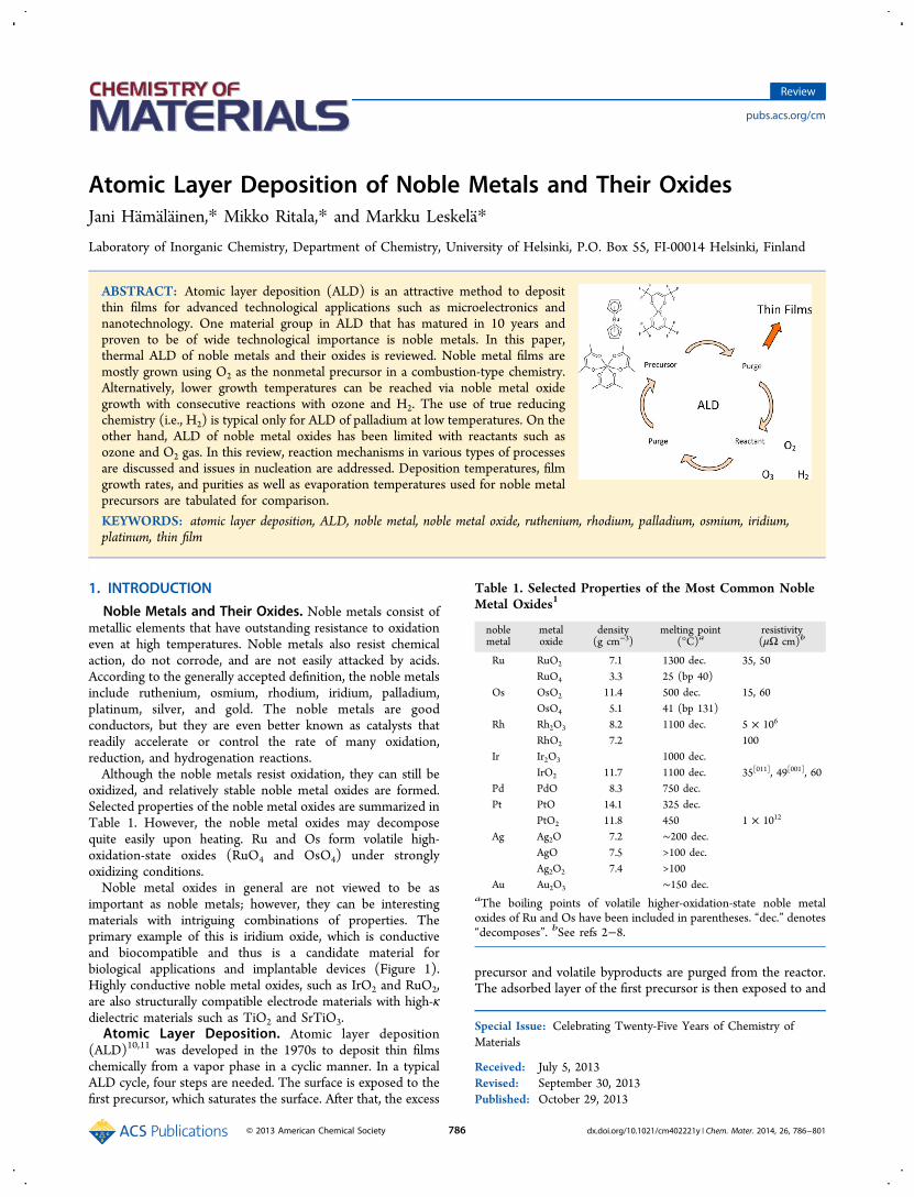
Thermal ALD processes for noble metals can be divided intothree classes on the basis of the applied reactant (Figure 3).
The most common are the O2-based processes, in whichdeposition temperatures of 200 °C and above have beenrequired for the film growth. The noble metal thin filmsdeposited with these processes include Ru, Os, Rh, Ir, and Pt.Also, Pd films have been deposited, but with limited success. Incontrast, the conventional reducing agents H2 and formalinhave been successfully used in the ALD of Pd. With theseprocesses, Pd films have been deposited below 200 °C. Noblemetals have been grown by ALD also via noble metal oxides attemperatures below 200 °C. Rh, Ir, and Pt metal films weredeposited by supplying ozone followed by H2 in every growthcycle. The success in Pd growth via palladium oxide has beenlimited. At temperatures above 200 °C, the ozone-basedprocesses also deposit metallic films directly, without H2.Although noble metals are commonly grown by ALD,
process development for noble metal oxides has been scarce.Thermal ALD of noble metal oxides with ozone has beenreported for Rh, Ir, Pd, and Pt (Figure 3). Rh2O3, IrO2, PdO,and PtOx films have been grown only at temperatures below200 °C. In general, the ALD noble metal oxide growth withozone is achieved only at temperatures lower than those usedto deposit the corresponding noble metals with O2. As noblemetal oxides can be reduced easily to metals, the ALD oxidegrowth can be converted to metal growth by addition of H2pulses, enabling the ALD of noble metal thin films at lowertemperatures than required with O2. In addition, RuO2 andIrO2 have been deposited with O2 at temperatures above 200°C but only by using carefully optimized growth parameters.Ruthenium. Ruthenium is one of the most attractive noble
metals with respect to cost and physical properties. Therefore, a
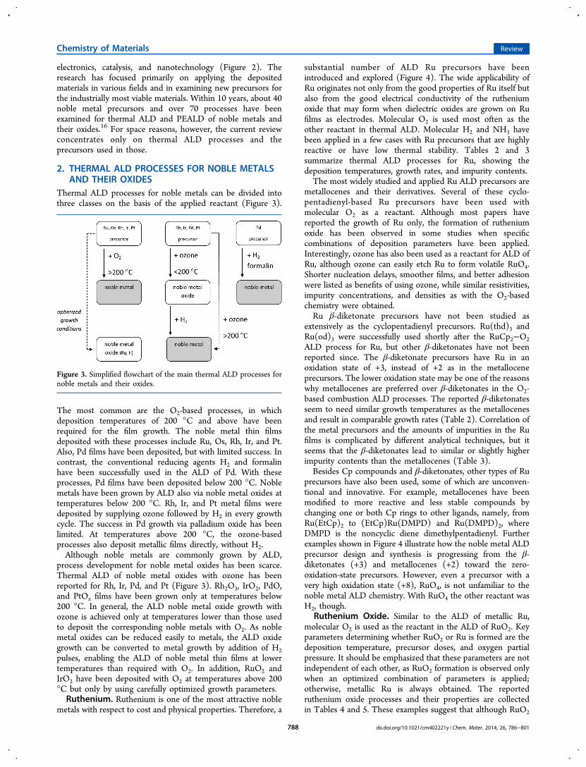
substantial number of ALD Ru precursors have beenintroduced and explored (Figure 4). The wide applicability ofRu originates not only from the good properties of Ru itself butalso from the good electrical conductivity of the rutheniumoxide that may form when dielectric oxides are grown on Rufilms as electrodes. Molecular O2 is used most often as theother reactant in thermal ALD. Molecular H2 and NH3 havebeen applied in a few cases with Ru precursors that are highlyreactive or have low thermal stability. Tables 2 and 3summarize thermal ALD processes for Ru, showing thedeposition temperatures, growth rates, and impurity contents.The most widely studied and applied Ru ALD precursors are
metallocenes and their derivatives. Several of these cyclo-pentadienyl-based Ru precursors have been used withmolecular O2 as a reactant. Although most papers havereported the growth of Ru only, the formation of rutheniumoxide has been observed in some studies when specificcombinations of deposition parameters have been applied.Interestingly, ozone has also been used as a reactant for ALD ofRu, although ozone can easily etch Ru to form volatile RuO4.Shorter nucleation delays, smoother films, and better adhesionwere listed as benefits of using ozone, while similar resistivities,impurity concentrations, and densities as with the O2-basedchemistry were obtained.Ru β-diketonate precursors have not been studied as
extensively as the cyclopentadienyl precursors. Ru(thd)3 andRu(od)3 were successfully used shortly after the RuCp2−O2ALD process for Ru, but other β-diketonates have not beenreported since. The β-diketonate precursors have Ru in anoxidation state of +3, instead of +2 as in the metalloceneprecursors. The lower oxidation state may be one of the reasonswhy metallocenes are preferred over β-diketonates in the O2-based combustion ALD processes. The reported β-diketonatesseem to need similar growth temperatures as the metallocenesand result in comparable growth rates (Table 2). Correlation ofthe metal precursors and the amounts of impurities in the Rufilms is complicated by different analytical techniques, but itseems that the β-diketonates lead to similar or slightly higherimpurity contents than the metallocenes (Table 3).Besides Cp compounds and β-diketonates, other types of Ru
precursors have also been used, some of which are unconven-tional and innovative. For example, metallocenes have beenmodified to more reactive and less stable compounds bychanging one or both Cp rings to other ligands, namely, fromRu(EtCp)2 to (EtCp)Ru(DMPD) and Ru(DMPD)2, whereDMPD is the noncyclic diene dimethylpentadienyl. Furtherexamples shown in Figure 4 illustrate how the noble metal ALDprecursor design and synthesis is progressing from the β-diketonates (+3) and metallocenes (+2) toward the zero-oxidation-state precursors. However, even a precursor with avery high oxidation state (+8), RuO4, is not unfamiliar to thenoble metal ALD chemistry. With RuO4 the other reactant wasH2, though.
Ruthenium Oxide. Similar to the ALD of metallic Ru,molecular O2 is used as the reactant in the ALD of RuO2. Keyparameters determining whether RuO2 or Ru is formed are thedeposition temperature, precursor doses, and oxygen partialpressure. It should be emphasized that these parameters are notindependent of each other, as RuO2 formation is observed onlywhen an optimized combination of parameters is applied;otherwise, metallic Ru is always obtained. The reportedruthenium oxide processes and their properties are collectedin Tables 4 and 5. These examples suggest that although RuO2
Figure 3. Simplified flowchart of the main thermal ALD processes fornoble metals and their oxides.
Chemistry of Materials Review
dx.doi.org/10.1021/cm402221y | Chem. Mater. 2014, 26, 786−801788
growth has not been verified with all Ru precursors, thedeposition should be feasible with metallocenes and β-diketonates as well as other precursors alike.Osmium. Osmium is a challenging metal because of its
hardness, brittleness, low vapor pressure, and very high meltingpoint, and it also oxidizes easily to either OsO2 or thedangerous, volatile OsO4. These characteristics explain thelimited interest in Os metal film deposition. Anyhow, Os filmgrowth has been demonstrated by ALD using OsCp2 and O2between 325 and 375 °C (Figure 5).102 The growth rates wereroughly 0.2 Å/cycle at 325 °C and 0.3 Å/cycle between 350and 375 °C. The films were very pure, containing less than 1atom % oxygen, carbon, and hydrogen impurities each. This isthe only report of Os film deposition by ALD, and no osmiumoxide ALD processes have been reported. An ozone-basedprocess would not be desirable because Os may easily oxidizeto the volatile OsO4 instead of OsO2 even at room temperature.However, the approaches used for ALD of RuO2 with O2should be feasible for ALD of OsO2 as well.Rhodium and Rhodium Oxide. Rh processes are one of
the least examined among the noble metal ALD processes. Theprocess development has been based solely on a single β-diketonate precursor, Rh(acac)3. The published Rh metal and
oxide ALD processes with their deposition temperatures,growth rates, and impurity contents are shown in Tables 6and 7.
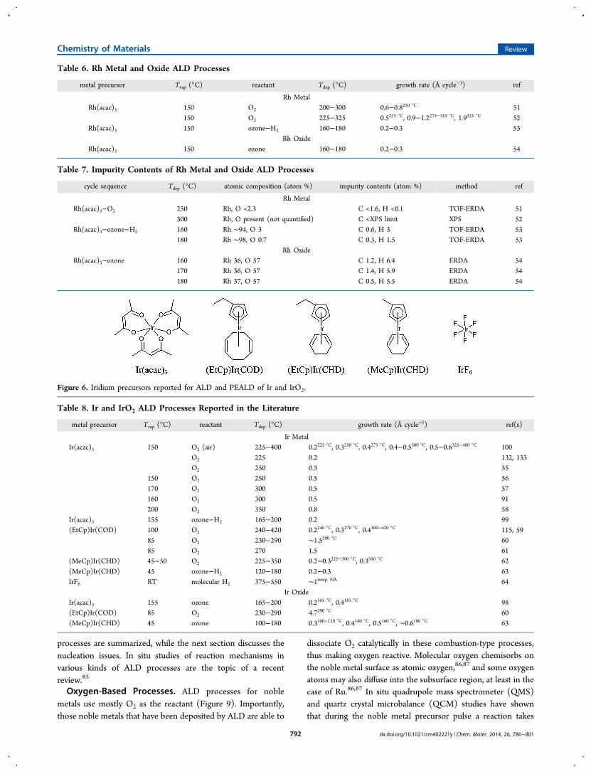
Iridium and Iridium Oxide. Various Ir precursors havebeen presented in the literature for thermal ALD processes forIr and IrO2 (Figure 6). The Ir thermal ALD processes are basedon either oxidative (combustion) chemistry, reductive chem-istry, or a combination of these two (Table 8). The combustionprocesses using molecular O2 are the most common also for theIr ALD. Iridium oxide thin films have been grown by ALDusing either ozone or O2 as an oxidant. Table 9 lists thereported impurity contents in the Ir metal and IrO2 films.
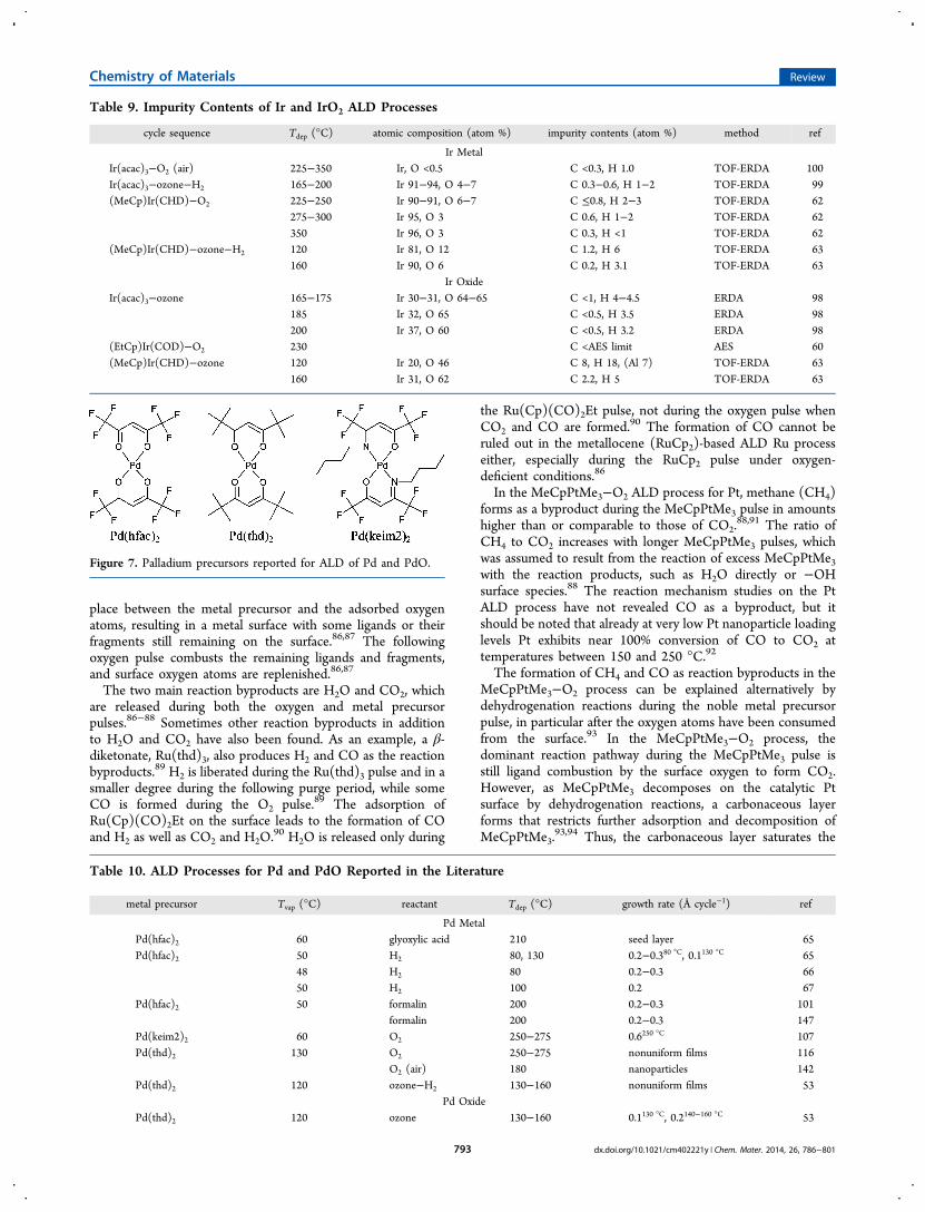
Palladium and Palladium Oxide. ALD processes for Pdhave been based on a single Pd precursor, namely, Pd(hfac)2,although the suitability of some other precursors has also beenexamined (Figure 7). Different from the other noble metalALD processes, the Pd processes rely mostly on true reducingagents rather than on the most common molecular oxygen(Table 10). Glyoxylic acid, molecular H2, and most commonlyformalin have been used to deposit Pd films. In contrast, theexploration of palladium oxide thin films has been very limited(Table 10). The impurity contents of the Pd and PdO films arecollected in Table 11.
Figure 4. Ruthenium precursors reported for Ru ALD processes.
Chemistry of Materials Review
dx.doi.org/10.1021/cm402221y | Chem. Mater. 2014, 26, 786−801789
Platinum and Platinum Oxide. Pt processes are the mostimportant noble metal ALD processes together with the Ru andIr processes because of the wide applicability of Pt. Surprisinglyenough, thermal ALD of Pt has relied nearly exclusively on asingle platinum precursor, MeCpPtMe3 (Tables 12 and 13). Incontrast, platinum oxide films have been grown using Pt(acac)2and ozone as the reactant (Tables 12 and 13). MeCpPtMe3 canbe used for ALD of platinum oxide as well; however, metalfilms can form easily instead of oxide at low temperatures.16
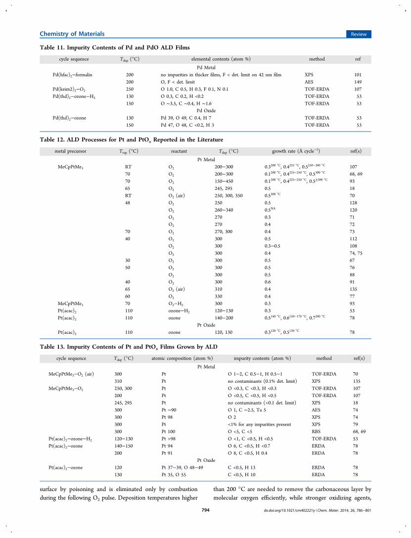
Silver. A combination of low thermal stability andinsufficient volatility of Ag precursor candidates makes thedevelopment of ALD processes for Ag particularly demanding.This is especially problematic when considering thermal ALD.
Some Ag precursors (Figure 8) have been successfully appliedfor PEALD of Ag films.80,81 These precursors contain eitherphosphine adducts or fluorinated ligands, some even both.Notably, such ligands are not common in other noble metalALD processes. The only report of thermal ALD of Ag usedAg(hfac)(COD) and propanol between 110 and 150 °C,82 butthis process resulted in nanoparticles rather than a continuousfilm.
Gold. There are currently no reported thermal ALDprocesses for gold and its oxide. Likewise, PEALD of Au hasbeen attempted but with only limited success.83 In general, thelack of proper Au precursors is a similar factor as in the case ofALD of Ag. It is expected that PEALD of Au similar to PEALD
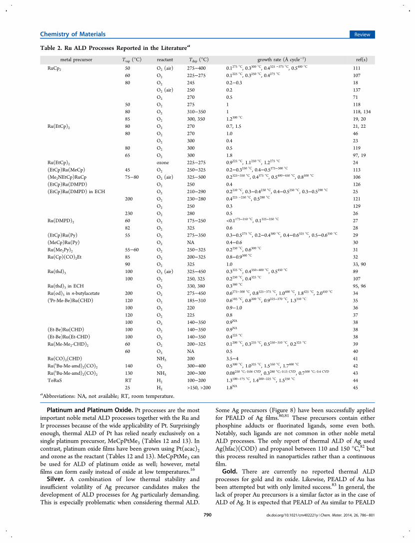
Table 2. Ru ALD Processes Reported in the Literaturea
metal precursor Tvap (°C) reactant Tdep (°C) growth rate (Å cycle−1) ref(s)
RuCp2 50 O2 (air) 275−400 0.1275 °C, 0.3300 °C, 0.4325 −375 °C, 0.5400 °C 11160 O2 225−275 0.1225 °C, 0.3250 °C, 0.4275 °C 10780 O2 245 0.2−0.3 18
O2 (air) 250 0.2 137O2 270 0.5 71
50 O2 275 1 11880 O2 310−350 1 118, 13485 O2 300, 350 1.2300 °C 19, 20
Ru(EtCp)2 80 O2 270 0.7, 1.5 21, 2280 O2 270 1.0 46
O2 300 0.4 2380 O2 300 0.5 11965 O2 300 1.8 97, 19
Ru(EtCp)2 ozone 225−275 0.9225 °C, 1.1250 °C, 1.2275 °C 24(EtCp)Ru(MeCp) 45 O2 250−325 0.2−0.3250 °C, 0.4−0.5275−300 °C 113(Me2NEtCp)RuCp 75−80 O2 (air) 325−500 0.2325−350 °C, 0.4375 °C, 0.5400−450 °C, 0.8500 °C 106(EtCp)Ru(DMPD) O2 250 0.4 126(EtCp)Ru(DMPD) in ECH O2 210−290 0.2210 °C, 0.3−0.4230 °C, 0.4−0.5250 °C, 0.3−0.5290 °C 25
200 O2 230−280 0.4225 −250 °C, 0.5280 °C 121O2 250 0.3 129
230 O2 280 0.5 26Ru(DMPD)2 60 O2 175−250 <0.1175−210 °C, 0.1225−250 °C 27
82 O2 325 0.6 28(EtCp)Ru(Py) 55 O2 275−350 0.3−0.5275 °C, 0.2−0.4300 °C, 0.4−0.6325 °C, 0.5−0.6350 °C 29(MeCp)Ru(Py) O2 NA 0.4−0.6 30Ru(Me2Py)2 55−60 O2 250−325 0.2250 °C, 0.6300 °C 31Ru(Cp)(CO)2Et 85 O2 200−325 0.8−0.9300 °C 32
90 O2 325 1.0 33, 90Ru(thd)3 100 O2 (air) 325−450 0.3325 °C, 0.4350−400 °C, 0.5450 °C 89
100 O2 250, 325 0.2250 °C, 0.4325 °C 107Ru(thd)3 in ECH O2 330, 380 0.3380 °C 95, 96Ru(od)3 in n-butylacetate 200 O2 275−450 0.6275−300 °C, 0.8325−375 °C, 1.0400 °C, 1.8425 °C, 2.0450 °C 34(iPr-Me-Be)Ru(CHD) 120 O2 185−310 0.6185 °C, 0.8200 °C, 0.9225−270 °C, 1.3310 °C 35
100 O2 220 0.9−1.0 36120 O2 225 0.8 37100 O2 140−350 0.9NA 38
(Et-Be)Ru(CHD) 100 O2 140−350 0.9NA 38(Et-Be)Ru(Et-CHD) 100 O2 140−350 0.4225 °C 38Ru(Me-Me2-CHD)2 60 O2 200−325 0.1200 °C, 0.3235 °C, 0.5250−310 °C, 0.2325 °C 39
60 O2 NA 0.5 40Ru(CO)3(CHD) NH3 200 3.5−4 41Ru(tBu-Me-amd)2(CO)2 140 O2 300−400 0.5300 °C, 1.0325 °C, 1.5350 °C, 1.7400 °C 42Ru(tBu-Me-amd)2(CO)2 130 NH3 200−300 0.08250 °C; 0.06 CVD, 0.3280 °C; 0.15 CVD, 0.7300 °C; 0.4 CVD 43ToRuS RT H2 100−200 1.3100−175 °C, 1.4200−225 °C, 1.5250 °C 44
25 H2 >150, >200 1.8NA 45aAbbreviations: NA, not available; RT, room temperature.
Chemistry of Materials Review
dx.doi.org/10.1021/cm402221y | Chem. Mater. 2014, 26, 786−801790

of Ag would be the most probable approach for Au film growth.Amidinates and guanidinates could be interesting precursors forAu PEALD and ALD processes; at least a gold guanidinate[Au(NiPr)2NMe2]2 sublimes at a low temperature (85 °C, 20mTorr) with a 4% residual mass left in TGA.84 The suitabilityof these precursors has not however been proven for ALD.
3. STEADY-STATE REACTION MECHANISMS
Reaction mechanism studies of the noble metal and noblemetal oxide ALD processes provide fundamental understandingof the ALD chemistry. The reaction mechanism during thesteady-state film growth has to be separated from the initialnucleation mechanism (i.e., the start of the film growth on thesubstrate surface). Here the steady-state reaction mechanismsin the main types of noble metal and noble metal oxide ALD
Table 3. Impurity Contents of Ru ALD Processes
cycle sequence Tdep (°C) impurity contents (atom %) method ref
Ru(Cp)2−O2 (air) 300 O <1.5, C <0.3, H <0.4 TOF-ERDA 111350 O <0.4, C <0.2, H <0.2 TOF-ERDA 111400 O <0.5, C <0.3, H <0.2 TOF-ERDA 111
Ru(Cp)2−O2 245 O in surface and in film AES 18Ru(EtCp)2−O2 270 O <2, C <2 TOF-ERDA, AES 21Ru(EtCp)2−ozone 275 O <1 AES 24(EtCp)Ru(DMPD) in ECH−O2 250, 280 O <AES limit AES 121
280 negligible O and C XPS 26Ru(DMPD)2−O2 325 O <1, C <0.2, N < 0.2 SIMS 28(EtCp)Ru(Py)−O2 275 O <2, C 0.6, H 2, N 0.5 TOF-ERDA 29(MeCp)Ru(Py)−O2 NA O 10, C <1.3, H <2 ERDA 30Ru(Me2Py)2−O2 275 O 3.6, C 1.6, H 3, N 1.2 TOF-ERDA 31Ru(thd)3−O2 (air) 350 O 4.1, C 1.2, H 2.2 TOF-ERDA 89Ru(thd)3 in ECH−O2 380 O <1 SIMS 95(iPr-Me-Be)Ru(CHD)−O2 220 O ∼4 XPS 36
225 O <SIMS limit, C ∼1.8 SIMS 37270 O <SIMS limit, C <SIMS limit SIMS 35310 O <SIMS limit, C ∼2.4 SIMS 35
Ru(tBu-Me-amd)2(CO)2−O2 NA O 0.3, C 0.3 APM 42Ru(tBu-Me-amd)2(CO)2−NH3 300 O ∼0.2%, C ∼0.05% SIMS 43
NA O, C, N < RBS limit RBS 43ToRuS−H2 100, 200 O 3, C 0.5−1, H <1, N < 1 ERDA 44
250 O <AES limit, C <AES limit AES 45
Table 4. RuOx and RuO2 ALD Processes Reported in the Literaturea
metal precursor Tvap (°C) reactant Tdep (°C) growth rate (Å cycle−1) ref(s)
RuCp2 85 O2 300 3.2 20Ru(EtCp)2 80 O2 270 1.5−1.7 21, 46
80 O2 280 0.3 4765 O2 300, 350 up to 7 (300 °C) 97
Ru(EtCp)2 (mod.) 135 O2 (also in pulses and purges) 265 1.4 48(EtCp)Ru(DMPD) in ECH (mod.) O2 (also in Ru prec. pulse) 250 NA 49Ru(DMPD)2 60 O2 175, 200 NA 27(MeCp)Ru(Py) O2 NA 0.7−0.8 30Ru(thd)2(cod) in pyridine O2 290 6.6 50Ru(Me-Me2-CHD)2 60 O2 NA NA 39
aAbbreviations: mod., modified ALD system; NA, not available.
Table 5. Impurity Contents of RuO2 ALD Processes
cycle sequence Tdep (°C) atomic composition (atom %) impurity contents (atom %) method ref
(MeCp)Ru(Py)−O2 NA Ru 34, O 57 C 0.1, H 1.4 ERDA 30Ru(thd)2(cod) in pyridine−O2 290 Ru, O C low, some N SIMS 50
Figure 5. Scanning electron micrographs of an ALD-grown Os film(bright line) deposited conformally in a deep trench. Reprinted withpermission from ref 102. Copyright 2011 American Chemical Society.
Chemistry of Materials Review
dx.doi.org/10.1021/cm402221y | Chem. Mater. 2014, 26, 786−801791
processes are summarized, while the next section discusses thenucleation issues. In situ studies of reaction mechanisms invarious kinds of ALD processes are the topic of a recentreview.85
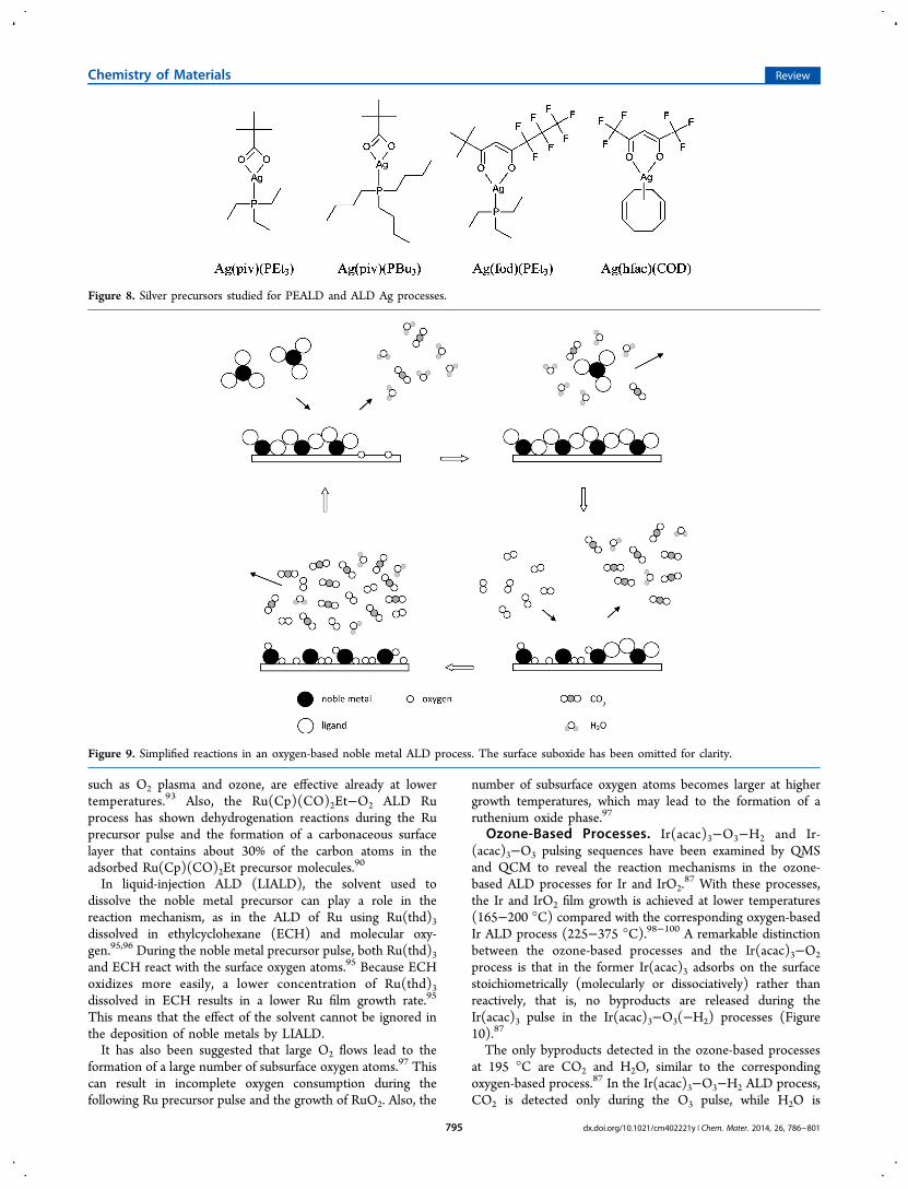
Oxygen-Based Processes. ALD processes for noblemetals use mostly O2 as the reactant (Figure 9). Importantly,those noble metals that have been deposited by ALD are able to
dissociate O2 catalytically in these combustion-type processes,thus making oxygen reactive. Molecular oxygen chemisorbs onthe noble metal surface as atomic oxygen,86,87 and some oxygenatoms may also diffuse into the subsurface region, at least in thecase of Ru.86,87 In situ quadrupole mass spectrometer (QMS)and quartz crystal microbalance (QCM) studies have shownthat during the noble metal precursor pulse a reaction takes
Table 6. Rh Metal and Oxide ALD Processes
metal precursor Tvap (°C) reactant Tdep (°C) growth rate (Å cycle−1) ref
Rh MetalRh(acac)3 150 O2 200−300 0.6−0.8250 °C 51
150 O2 225−325 0.5225 °C, 0.9−1.2275−310 °C, 1.9325 °C 52Rh(acac)3 150 ozone−H2 160−180 0.2−0.3 53
Rh OxideRh(acac)3 150 ozone 160−180 0.2−0.3 54
Table 7. Impurity Contents of Rh Metal and Oxide ALD Processes
cycle sequence Tdep (°C) atomic composition (atom %) impurity contents (atom %) method ref
Rh MetalRh(acac)3−O2 250 Rh, O <2.3 C <1.6, H <0.1 TOF-ERDA 51
300 Rh, O present (not quantified) C <XPS limit XPS 52Rh(acac)3−ozone−H2 160 Rh ∼94, O 3 C 0.6, H 3 TOF-ERDA 53
180 Rh ∼98, O 0.7 C 0.3, H 1.5 TOF-ERDA 53Rh Oxide
Rh(acac)3−ozone 160 Rh 36, O 57 C 1.2, H 6.4 ERDA 54170 Rh 36, O 57 C 1.4, H 5.9 ERDA 54180 Rh 37, O 57 C 0.5, H 5.5 ERDA 54
Figure 6. Iridium precursors reported for ALD and PEALD of Ir and IrO2.
Table 8. Ir and IrO2 ALD Processes Reported in the Literature
metal precursor Tvap (°C) reactant Tdep (°C) growth rate (Å cycle−1) ref(s)
Ir MetalIr(acac)3 150 O2 (air) 225−400 0.2225 °C, 0.3250 °C, 0.4275 °C, 0.4−0.5300 °C, 0.5−0.6325−400 °C 100
O2 225 0.2 132, 133O2 250 0.3 55
150 O2 250 0.5 56170 O2 300 0.5 57160 O2 300 0.5 91200 O2 350 0.8 58
Ir(acac)3 155 ozone−H2 165−200 0.2 99(EtCp)Ir(COD) 100 O2 240−420 0.2240 °C, 0.3270 °C, 0.4300−420 °C 115, 59
85 O2 230−290 ∼1.5290 °C 6085 O2 270 1.5 61
(MeCp)Ir(CHD) 45−50 O2 225−350 0.2−0.3225−300 °C, 0.3350 °C 62(MeCp)Ir(CHD) 45 ozone−H2 120−180 0.2−0.3 63IrF6 RT molecular H2 375−550 ∼1temp. NA 64
Ir OxideIr(acac)3 155 ozone 165−200 0.2165 °C, 0.4185 °C 98(EtCp)Ir(COD) 85 O2 230−290 4.7290 °C 60(MeCp)Ir(CHD) 45 ozone 100−180 0.3100−120 °C, 0.4140 °C, 0.5160 °C, ∼0.6180 °C 63
Chemistry of Materials Review
dx.doi.org/10.1021/cm402221y | Chem. Mater. 2014, 26, 786−801792
place between the metal precursor and the adsorbed oxygenatoms, resulting in a metal surface with some ligands or theirfragments still remaining on the surface.86,87 The followingoxygen pulse combusts the remaining ligands and fragments,and surface oxygen atoms are replenished.86,87
The two main reaction byproducts are H2O and CO2, whichare released during both the oxygen and metal precursorpulses.86−88 Sometimes other reaction byproducts in additionto H2O and CO2 have also been found. As an example, a β-diketonate, Ru(thd)3, also produces H2 and CO as the reactionbyproducts.89 H2 is liberated during the Ru(thd)3 pulse and in asmaller degree during the following purge period, while someCO is formed during the O2 pulse.89 The adsorption ofRu(Cp)(CO)2Et on the surface leads to the formation of COand H2 as well as CO2 and H2O.
90 H2O is released only during
the Ru(Cp)(CO)2Et pulse, not during the oxygen pulse whenCO2 and CO are formed.90 The formation of CO cannot beruled out in the metallocene (RuCp2)-based ALD Ru processeither, especially during the RuCp2 pulse under oxygen-deficient conditions.86
In the MeCpPtMe3−O2 ALD process for Pt, methane (CH4)forms as a byproduct during the MeCpPtMe3 pulse in amountshigher than or comparable to those of CO2.
88,91 The ratio ofCH4 to CO2 increases with longer MeCpPtMe3 pulses, whichwas assumed to result from the reaction of excess MeCpPtMe3with the reaction products, such as H2O directly or −OHsurface species.88 The reaction mechanism studies on the PtALD process have not revealed CO as a byproduct, but itshould be noted that already at very low Pt nanoparticle loadinglevels Pt exhibits near 100% conversion of CO to CO2 attemperatures between 150 and 250 °C.92
The formation of CH4 and CO as reaction byproducts in theMeCpPtMe3−O2 process can be explained alternatively bydehydrogenation reactions during the noble metal precursorpulse, in particular after the oxygen atoms have been consumedfrom the surface.93 In the MeCpPtMe3−O2 process, thedominant reaction pathway during the MeCpPtMe3 pulse isstill ligand combustion by the surface oxygen to form CO2.However, as MeCpPtMe3 decomposes on the catalytic Ptsurface by dehydrogenation reactions, a carbonaceous layerforms that restricts further adsorption and decomposition ofMeCpPtMe3.
93,94 Thus, the carbonaceous layer saturates the
Table 9. Impurity Contents of Ir and IrO2 ALD Processes
cycle sequence Tdep (°C) atomic composition (atom %) impurity contents (atom %) method ref
Ir MetalIr(acac)3−O2 (air) 225−350 Ir, O <0.5 C <0.3, H 1.0 TOF-ERDA 100Ir(acac)3−ozone−H2 165−200 Ir 91−94, O 4−7 C 0.3−0.6, H 1−2 TOF-ERDA 99(MeCp)Ir(CHD)−O2 225−250 Ir 90−91, O 6−7 C ≤0.8, H 2−3 TOF-ERDA 62
275−300 Ir 95, O 3 C 0.6, H 1−2 TOF-ERDA 62350 Ir 96, O 3 C 0.3, H <1 TOF-ERDA 62
(MeCp)Ir(CHD)−ozone−H2 120 Ir 81, O 12 C 1.2, H 6 TOF-ERDA 63160 Ir 90, O 6 C 0.2, H 3.1 TOF-ERDA 63
Ir OxideIr(acac)3−ozone 165−175 Ir 30−31, O 64−65 C <1, H 4−4.5 ERDA 98
185 Ir 32, O 65 C <0.5, H 3.5 ERDA 98200 Ir 37, O 60 C <0.5, H 3.2 ERDA 98
(EtCp)Ir(COD)−O2 230 C <AES limit AES 60(MeCp)Ir(CHD)−ozone 120 Ir 20, O 46 C 8, H 18, (Al 7) TOF-ERDA 63
160 Ir 31, O 62 C 2.2, H 5 TOF-ERDA 63
Figure 7. Palladium precursors reported for ALD of Pd and PdO.
Table 10. ALD Processes for Pd and PdO Reported in the Literature
metal precursor Tvap (°C) reactant Tdep (°C) growth rate (Å cycle−1) ref
Pd MetalPd(hfac)2 60 glyoxylic acid 210 seed layer 65Pd(hfac)2 50 H2 80, 130 0.2−0.380 °C, 0.1130 °C 65
48 H2 80 0.2−0.3 6650 H2 100 0.2 67
Pd(hfac)2 50 formalin 200 0.2−0.3 101formalin 200 0.2−0.3 147
Pd(keim2)2 60 O2 250−275 0.6250 °C 107Pd(thd)2 130 O2 250−275 nonuniform films 116
O2 (air) 180 nanoparticles 142Pd(thd)2 120 ozone−H2 130−160 nonuniform films 53
Pd OxidePd(thd)2 120 ozone 130−160 0.1130 °C, 0.2140−160 °C 53
Chemistry of Materials Review
dx.doi.org/10.1021/cm402221y | Chem. Mater. 2014, 26, 786−801793
surface by poisoning and is eliminated only by combustionduring the following O2 pulse. Deposition temperatures higher
than 200 °C are needed to remove the carbonaceous layer bymolecular oxygen efficiently, while stronger oxidizing agents,
Table 11. Impurity Contents of Pd and PdO ALD Films
cycle sequence Tdep (°C) elemental contents (atom %) method ref
Pd MetalPd(hfac)2−formalin 200 no impurities in thicker films, F < det. limit on 42 nm film XPS 101
200 O, F < det. limit AES 149Pd(keim2)2−O2 250 O 1.0, C 0.5, H 0.3, F 0.1, N 0.1 TOF-ERDA 107Pd(thd)2−ozone−H2 130 O 0.3, C 0.2, H <0.2 TOF-ERDA 53
150 O ∼3.5, C ∼0.4, H ∼1.6 TOF-ERDA 53Pd Oxide
Pd(thd)2−ozone 130 Pd 39, O 49, C 0.4, H 7 TOF-ERDA 53150 Pd 47, O 48, C <0.2, H 3 TOF-ERDA 53
Table 12. ALD Processes for Pt and PtOx Reported in the Literature
metal precursor Tvap (°C) reactant Tdep (°C) growth rate (Å cycle−1) ref(s)
Pt MetalMeCpPtMe3 RT O2 200−300 0.3200 °C, 0.4225 °C, 0.5250−300 °C 107
70 O2 200−300 0.1200 °C, 0.4225−250 °C, 0.5300 °C 68, 6970 O2 150−450 0.1200 °C, 0.4225−250 °C, 0.5≥300 °C 9365 O2 245, 295 0.5 18RT O2 (air) 250, 300, 350 0.5300 °C 7048 O2 250 0.5 128
O2 260−340 0.5NA 120O2 270 0.3 71O2 270 0.4 72
70 O2 270, 300 0.4 7340 O2 300 0.5 112
O2 300 0.3−0.5 108O2 300 0.4 74, 75
30 O2 300 0.5 6750 O2 300 0.5 76
O2 300 0.5 8840 O2 300 0.6 9165 O2 (air) 310 0.4 13560 O2 330 0.4 77
MeCpPtMe3 70 O2−H2 300 0.3 93Pt(acac)2 110 ozone−H2 120−130 0.3 53Pt(acac)2 110 ozone 140−200 0.5140 °C, 0.6150−170 °C, 0.7200 °C 78
Pt OxidePt(acac)2 110 ozone 120, 130 0.3120 °C, 0.5130 °C 78
Table 13. Impurity Contents of Pt and PtOx Films Grown by ALD
cycle sequence Tdep (°C) atomic composition (atom %) impurity contents (atom %) method ref(s)
Pt MetalMeCpPtMe3−O2 (air) 300 Pt O 1−2, C 0.5−1, H 0.5−1 TOF-ERDA 70
310 Pt no contaminants (0.1% det. limit) XPS 135MeCpPtMe3−O2 250, 300 Pt O <0.3, C <0.3, H <0.3 TOF-ERDA 107
200 Pt O <0.5, C <0.5, H <0.5 TOF-ERDA 107245, 295 Pt no contaminants (<0.1 det. limit) XPS 18300 Pt ∼90 O 1, C ∼2.5, Ta 5 AES 74300 Pt 98 O 2 XPS 74300 Pt <1% for any impurities present XPS 79300 Pt 100 O <5, C <5 RBS 68, 69
Pt(acac)2−ozone−H2 120−130 Pt >98 O <1, C <0.5, H <0.5 TOF-ERDA 53Pt(acac)2−ozone 140−150 Pt 94 O 6, C <0.5, H <0.7 ERDA 78
200 Pt 91 O 8, C <0.5, H 0.4 ERDA 78Pt Oxide
Pt(acac)2−ozone 120 Pt 37−39, O 48−49 C <0.5, H 13 ERDA 78130 Pt 35, O 55 C <0.5, H 10 ERDA 78
Chemistry of Materials Review
dx.doi.org/10.1021/cm402221y | Chem. Mater. 2014, 26, 786−801794
such as O2 plasma and ozone, are effective already at lowertemperatures.93 Also, the Ru(Cp)(CO)2Et−O2 ALD Ruprocess has shown dehydrogenation reactions during the Ruprecursor pulse and the formation of a carbonaceous surfacelayer that contains about 30% of the carbon atoms in theadsorbed Ru(Cp)(CO)2Et precursor molecules.90
In liquid-injection ALD (LIALD), the solvent used todissolve the noble metal precursor can play a role in thereaction mechanism, as in the ALD of Ru using Ru(thd)3dissolved in ethylcyclohexane (ECH) and molecular oxy-gen.95,96 During the noble metal precursor pulse, both Ru(thd)3and ECH react with the surface oxygen atoms.95 Because ECHoxidizes more easily, a lower concentration of Ru(thd)3dissolved in ECH results in a lower Ru film growth rate.95
This means that the effect of the solvent cannot be ignored inthe deposition of noble metals by LIALD.It has also been suggested that large O2 flows lead to the
formation of a large number of subsurface oxygen atoms.97 Thiscan result in incomplete oxygen consumption during thefollowing Ru precursor pulse and the growth of RuO2. Also, the
number of subsurface oxygen atoms becomes larger at highergrowth temperatures, which may lead to the formation of aruthenium oxide phase.97
Ozone-Based Processes. Ir(acac)3−O3−H2 and Ir-(acac)3−O3 pulsing sequences have been examined by QMSand QCM to reveal the reaction mechanisms in the ozone-based ALD processes for Ir and IrO2.
87 With these processes,the Ir and IrO2 film growth is achieved at lower temperatures(165−200 °C) compared with the corresponding oxygen-basedIr ALD process (225−375 °C).98−100 A remarkable distinctionbetween the ozone-based processes and the Ir(acac)3−O2
process is that in the former Ir(acac)3 adsorbs on the surfacestoichiometrically (molecularly or dissociatively) rather thanreactively, that is, no byproducts are released during theIr(acac)3 pulse in the Ir(acac)3−O3(−H2) processes (Figure10).87
The only byproducts detected in the ozone-based processesat 195 °C are CO2 and H2O, similar to the correspondingoxygen-based process.87 In the Ir(acac)3−O3−H2 ALD process,CO2 is detected only during the O3 pulse, while H2O is
Figure 8. Silver precursors studied for PEALD and ALD Ag processes.
Figure 9. Simplified reactions in an oxygen-based noble metal ALD process. The surface suboxide has been omitted for clarity.
Chemistry of Materials Review
dx.doi.org/10.1021/cm402221y | Chem. Mater. 2014, 26, 786−801795
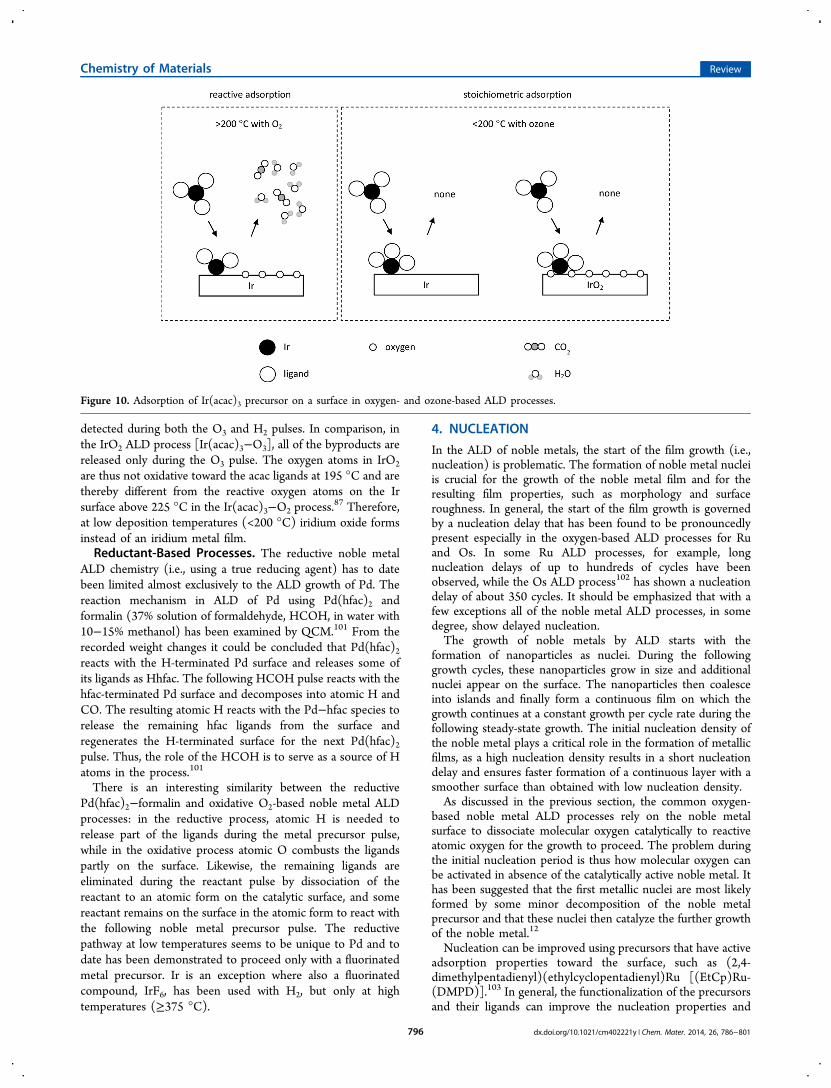
detected during both the O3 and H2 pulses. In comparison, inthe IrO2 ALD process [Ir(acac)3−O3], all of the byproducts arereleased only during the O3 pulse. The oxygen atoms in IrO2
are thus not oxidative toward the acac ligands at 195 °C and arethereby different from the reactive oxygen atoms on the Irsurface above 225 °C in the Ir(acac)3−O2 process.
87 Therefore,at low deposition temperatures (<200 °C) iridium oxide formsinstead of an iridium metal film.Reductant-Based Processes. The reductive noble metal
ALD chemistry (i.e., using a true reducing agent) has to datebeen limited almost exclusively to the ALD growth of Pd. Thereaction mechanism in ALD of Pd using Pd(hfac)2 andformalin (37% solution of formaldehyde, HCOH, in water with10−15% methanol) has been examined by QCM.101 From therecorded weight changes it could be concluded that Pd(hfac)2reacts with the H-terminated Pd surface and releases some ofits ligands as Hhfac. The following HCOH pulse reacts with thehfac-terminated Pd surface and decomposes into atomic H andCO. The resulting atomic H reacts with the Pd−hfac species torelease the remaining hfac ligands from the surface andregenerates the H-terminated surface for the next Pd(hfac)2pulse. Thus, the role of the HCOH is to serve as a source of Hatoms in the process.101
There is an interesting similarity between the reductivePd(hfac)2−formalin and oxidative O2-based noble metal ALDprocesses: in the reductive process, atomic H is needed torelease part of the ligands during the metal precursor pulse,while in the oxidative process atomic O combusts the ligandspartly on the surface. Likewise, the remaining ligands areeliminated during the reactant pulse by dissociation of thereactant to an atomic form on the catalytic surface, and somereactant remains on the surface in the atomic form to react withthe following noble metal precursor pulse. The reductivepathway at low temperatures seems to be unique to Pd and todate has been demonstrated to proceed only with a fluorinatedmetal precursor. Ir is an exception where also a fluorinatedcompound, IrF6, has been used with H2, but only at hightemperatures (≥375 °C).
4. NUCLEATION
In the ALD of noble metals, the start of the film growth (i.e.,nucleation) is problematic. The formation of noble metal nucleiis crucial for the growth of the noble metal film and for theresulting film properties, such as morphology and surfaceroughness. In general, the start of the film growth is governedby a nucleation delay that has been found to be pronouncedlypresent especially in the oxygen-based ALD processes for Ruand Os. In some Ru ALD processes, for example, longnucleation delays of up to hundreds of cycles have beenobserved, while the Os ALD process102 has shown a nucleationdelay of about 350 cycles. It should be emphasized that with afew exceptions all of the noble metal ALD processes, in somedegree, show delayed nucleation.The growth of noble metals by ALD starts with the
formation of nanoparticles as nuclei. During the followinggrowth cycles, these nanoparticles grow in size and additionalnuclei appear on the surface. The nanoparticles then coalesceinto islands and finally form a continuous film on which thegrowth continues at a constant growth per cycle rate during thefollowing steady-state growth. The initial nucleation density ofthe noble metal plays a critical role in the formation of metallicfilms, as a high nucleation density results in a short nucleationdelay and ensures faster formation of a continuous layer with asmoother surface than obtained with low nucleation density.As discussed in the previous section, the common oxygen-
based noble metal ALD processes rely on the noble metalsurface to dissociate molecular oxygen catalytically to reactiveatomic oxygen for the growth to proceed. The problem duringthe initial nucleation period is thus how molecular oxygen canbe activated in absence of the catalytically active noble metal. Ithas been suggested that the first metallic nuclei are most likelyformed by some minor decomposition of the noble metalprecursor and that these nuclei then catalyze the further growthof the noble metal.12
Nucleation can be improved using precursors that have activeadsorption properties toward the surface, such as (2,4-dimethylpentadienyl)(ethylcyclopentadienyl)Ru [(EtCp)Ru-(DMPD)].103 In general, the functionalization of the precursorsand their ligands can improve the nucleation properties and
Figure 10. Adsorption of Ir(acac)3 precursor on a surface in oxygen- and ozone-based ALD processes.
Chemistry of Materials Review
dx.doi.org/10.1021/cm402221y | Chem. Mater. 2014, 26, 786−801796
thus decrease the nucleation delay. As an example, thecyclopentadienyl ligand is considered highly stable, but whenone of the cyclopentadienyl (EtCp) ligands from a metalloceneis opened to give a noncyclic diene (DMPD), as in(EtCp)Ru(DMPD), the precursor becomes more reactive.104
Also, feeding the noble metal precursor twice in every cycle canbe used to increase the nucleation density by enhancing thesurface saturation by the adsorbed precursor.105
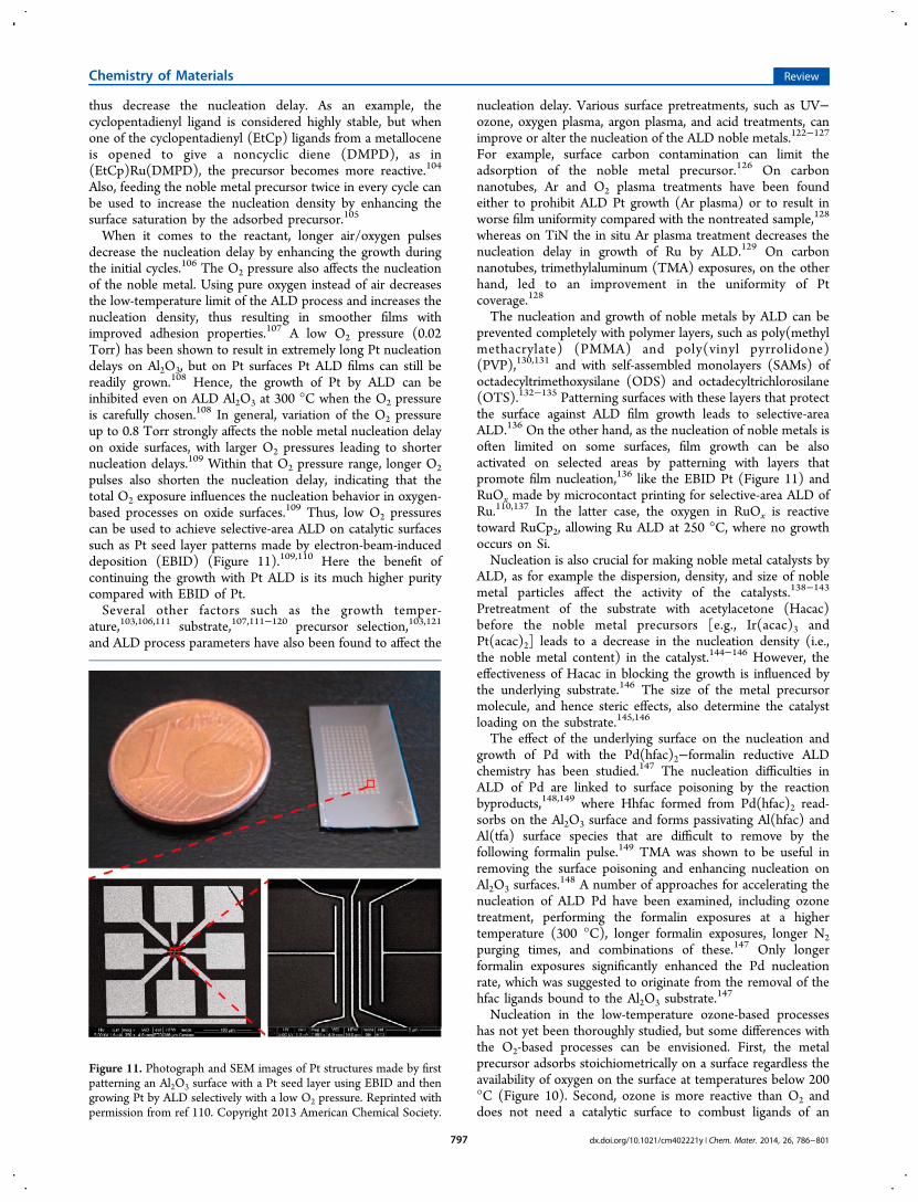
When it comes to the reactant, longer air/oxygen pulsesdecrease the nucleation delay by enhancing the growth duringthe initial cycles.106 The O2 pressure also affects the nucleationof the noble metal. Using pure oxygen instead of air decreasesthe low-temperature limit of the ALD process and increases thenucleation density, thus resulting in smoother films withimproved adhesion properties.107 A low O2 pressure (0.02Torr) has been shown to result in extremely long Pt nucleationdelays on Al2O3, but on Pt surfaces Pt ALD films can still bereadily grown.108 Hence, the growth of Pt by ALD can beinhibited even on ALD Al2O3 at 300 °C when the O2 pressureis carefully chosen.108 In general, variation of the O2 pressureup to 0.8 Torr strongly affects the noble metal nucleation delayon oxide surfaces, with larger O2 pressures leading to shorternucleation delays.109 Within that O2 pressure range, longer O2pulses also shorten the nucleation delay, indicating that thetotal O2 exposure influences the nucleation behavior in oxygen-based processes on oxide surfaces.109 Thus, low O2 pressurescan be used to achieve selective-area ALD on catalytic surfacessuch as Pt seed layer patterns made by electron-beam-induceddeposition (EBID) (Figure 11).109,110 Here the benefit ofcontinuing the growth with Pt ALD is its much higher puritycompared with EBID of Pt.Several other factors such as the growth temper-
ature,103,106,111 substrate,107,111−120 precursor selection,103,121
and ALD process parameters have also been found to affect the
nucleation delay. Various surface pretreatments, such as UV−ozone, oxygen plasma, argon plasma, and acid treatments, canimprove or alter the nucleation of the ALD noble metals.122−127
For example, surface carbon contamination can limit theadsorption of the noble metal precursor.126 On carbonnanotubes, Ar and O2 plasma treatments have been foundeither to prohibit ALD Pt growth (Ar plasma) or to result inworse film uniformity compared with the nontreated sample,128
whereas on TiN the in situ Ar plasma treatment decreases thenucleation delay in growth of Ru by ALD.129 On carbonnanotubes, trimethylaluminum (TMA) exposures, on the otherhand, led to an improvement in the uniformity of Ptcoverage.128
The nucleation and growth of noble metals by ALD can beprevented completely with polymer layers, such as poly(methylmethacrylate) (PMMA) and poly(vinyl pyrrolidone)(PVP),130,131 and with self-assembled monolayers (SAMs) ofoctadecyltrimethoxysilane (ODS) and octadecyltrichlorosilane(OTS).132−135 Patterning surfaces with these layers that protectthe surface against ALD film growth leads to selective-areaALD.136 On the other hand, as the nucleation of noble metals isoften limited on some surfaces, film growth can be alsoactivated on selected areas by patterning with layers thatpromote film nucleation,136 like the EBID Pt (Figure 11) andRuOx made by microcontact printing for selective-area ALD ofRu.110,137 In the latter case, the oxygen in RuOx is reactivetoward RuCp2, allowing Ru ALD at 250 °C, where no growthoccurs on Si.Nucleation is also crucial for making noble metal catalysts by
ALD, as for example the dispersion, density, and size of noblemetal particles affect the activity of the catalysts.138−143
Pretreatment of the substrate with acetylacetone (Hacac)before the noble metal precursors [e.g., Ir(acac)3 andPt(acac)2] leads to a decrease in the nucleation density (i.e.,the noble metal content) in the catalyst.144−146 However, theeffectiveness of Hacac in blocking the growth is influenced bythe underlying substrate.146 The size of the metal precursormolecule, and hence steric effects, also determine the catalystloading on the substrate.145,146
The effect of the underlying surface on the nucleation andgrowth of Pd with the Pd(hfac)2−formalin reductive ALDchemistry has been studied.147 The nucleation difficulties inALD of Pd are linked to surface poisoning by the reactionbyproducts,148,149 where Hhfac formed from Pd(hfac)2 read-sorbs on the Al2O3 surface and forms passivating Al(hfac) andAl(tfa) surface species that are difficult to remove by thefollowing formalin pulse.149 TMA was shown to be useful inremoving the surface poisoning and enhancing nucleation onAl2O3 surfaces.
148 A number of approaches for accelerating thenucleation of ALD Pd have been examined, including ozonetreatment, performing the formalin exposures at a highertemperature (300 °C), longer formalin exposures, longer N2purging times, and combinations of these.147 Only longerformalin exposures significantly enhanced the Pd nucleationrate, which was suggested to originate from the removal of thehfac ligands bound to the Al2O3 substrate.
147
Nucleation in the low-temperature ozone-based processeshas not yet been thoroughly studied, but some differences withthe O2-based processes can be envisioned. First, the metalprecursor adsorbs stoichiometrically on a surface regardless theavailability of oxygen on the surface at temperatures below 200°C (Figure 10). Second, ozone is more reactive than O2 anddoes not need a catalytic surface to combust ligands of an
Figure 11. Photograph and SEM images of Pt structures made by firstpatterning an Al2O3 surface with a Pt seed layer using EBID and thengrowing Pt by ALD selectively with a low O2 pressure. Reprinted withpermission from ref 110. Copyright 2013 American Chemical Society.
Chemistry of Materials Review
dx.doi.org/10.1021/cm402221y | Chem. Mater. 2014, 26, 786−801797

adsorbed noble metal precursor. The combination of thestoichiometric adsorption of the noble metal precursor and theuse of reactive ozone allows the ozone-based processes tonucleate easily. This has been exploited in the ozone-basedALD of Ir, IrO2, and PtOx directly on PVP,150 which is apolymer that effectively blocks the growth of noble metals bythe oxygen-based ALD processes (Figure 12).131,150
5. SUMMARY AND CONCLUSIONSResearch on thermal ALD of noble metal thin films has beenvery active since the first reports in 2003. Substantial effort hasbeen devoted to the development of new ALD processes usingvarious noble metal precursors and reactants and to under-standing how the noble metal films grow by examining reactionmechanisms and nucleation behavior on various startingsurfaces. By far the most widely studied and applied noblemetal ALD processes are thermal O2-based processes, which areapplicable for most of the noble metals, currently excludingonly silver and gold. These combustion-type processes result inpure noble metal films and are not very dependent on the metalprecursors but require deposition temperatures above 200 °C.
In contrast, reductant-based noble metal ALD chemistry hasbeen successful only in rare cases, namely, ALD of Pd fromPd(hfac)2 at 80−200 °C and Ir from IrF6 at 375 °C and above.In these processes, H2 and formalin have been applied asreducing agents.The growth of noble metal oxides has been far more limited
compared with the noble metals. O2 has been used to growIrO2 and RuO2 at the same temperatures as the correspondingnoble metals, but this requires delicate control of the growthparameters to suppress metal formation. Oxides can be grownmore easily with ozone at lower temperatures (below 200 °C),as demonstrated with oxides of Ir, Rh, Pt, and Pd. However, theozone-based noble metal oxide processes are limited to narrowdeposition temperature ranges between the precursor evapo-ration temperatures and the reduction to the metal at about 200°C. The corresponding metal films can be grown also by addinga reductive H2 step after every noble metal oxide growth cycle,that is, by using a metal precursor−ozone−H2 pulsingsequence. This oxidation−reduction reaction pathway leads tothe thermal ALD of noble metals at temperatures lower thanpossible with the corresponding O2-based noble metal ALDprocesses. On the basis of the IrO2 and PtOx results, the lowesttemperature where the ozone-based chemistry is still effective islikely about 100−120 °C. However, the ozone-based chemistryis not desirable for Ru and Os, as these metals can oxidize easilyto volatile higher-oxidation-state oxides (RuO4, OsO4).In the O2-based processes, a catalytically active noble metal
surface is needed to activate O2 by dissociating it to atomic Oso that the ligands of the noble metal precursor are combustedand the film is grown. The requirement of O2 dissociation alsoexplains the need for deposition temperatures above 200 °Cand the difficulties in nucleation on various surfaces that are notcatalytically active in dissociating O2. The reductive ALDprocesses for Pd deposit films at temperatures as low as 80 °C,but the surface must also in this case be active in dissociatingH2 to atomic H. By contrast, in the ozone-based processes,already below 200 °C ozone is highly reactive even withoutcatalytically active surfaces and combusts the ligands to volatilebyproducts. In situ reaction mechanism studies have indicatedthat in the ozone-based Ir and IrO2 processes, the iridiumprecursor Ir(acac)3 adsorbs on the surface stoichiometricallyregardless the presence (IrO2) or absence (Ir) of oxygen on thesurface. The stoichiometric adsorption of the noble metalprecursor and the high reactivity of ozone allow the ozone-based processes to nucleate easily on various surfaces. However,the nucleation in the ozone-based processes on varioussubstrates has not yet been examined in detail, and thus, thepossibility of using the low-temperature ozone-based noblemetals and oxides for nonselective ALD on their own or asnucleation layers for the oxygen-based processes can only besuggested.
■ AUTHOR INFORMATION
Corresponding Authors*E-mail: [email protected].*E-mail: [email protected].*E-mail: [email protected]. Fax: +358 9 191 50198.
NotesThe authors declare no competing financial interest.
Figure 12. Effect of the reactant in ALD with Ir(acac)3 as the metalprecursor on a surface containing electrospun PVP fibers. (a) Imageshowing the results of selective-area ALD of Ir, where the PVP fiberprevented the growth of Ir by the Ir(acac)3−O2 process at 250 °C. (b)FESEM image of IrO2 nanotubes obtained by depositing IrO2 on PVPfibers at 165 °C from Ir(acac)3 and ozone and then calcining thestructure to remove the PVP fiber template. The image in (a) isreprinted with permission from ref 131. Copyright 2009 TheElectrochemical Society. The image in (b) is reprinted with permissionfrom ref 150. Copyright 2009 American Scientific Publishers.
Chemistry of Materials Review
dx.doi.org/10.1021/cm402221y | Chem. Mater. 2014, 26, 786−801798

■ ACKNOWLEDGMENTS
Financial support from ASM Microchemistry and the FinnishCentre of Excellence in Atomic Layer Deposition (Academy ofFinland) is gratefully acknowledged.
■ REFERENCES(1) CRC Handbook of Chemistry and Physics, 92nd ed. (Internetversion); CRC Press: Boca Raton, FL, 2012.(2) Ryden, W. D.; Lawson, A. W.; Sartain, C. C. Phys. Rev. B 1970, 1,1494.(3) Yen, P. C.; Chen, R. S.; Chen, C. C.; Huang, Y. S.; Tiong, K. K. J.Cryst. Growth 2004, 262, 271.(4) Roy, A.; Ghose, J. Mater. Res. Bull. 1998, 33, 547.(5) Shannon, R. D. Solid State Commun. 1968, 6, 139.(6) Shannon, R. D. Solid State Commun. 1969, 7, 257.(7) Pearsall, T. P.; Lee, C. A. Phys. Rev. B 1974, 10, 2190.(8) Rogers, D. B.; Shannon, R. D.; Sleight, A. W.; Gillson, J. L. Inorg.Chem. 1969, 8, 841.(9) Ryynanen, T.; Yla-Outinen, L.; Narkilahti, S.; Tanskanen, J. M.A.; Hyttinen, J.; Hamalainen, J.; Leskela, M.; Lekkala, J. J. Vac. Sci.Technol., A 2012, 30, No. 041501.(10) Ritala, M.; Leskela, M. In Handbook of Thin Film Materials;Nalwa, H. S., Ed.; Academic Press: San Diego, CA, 2001; Vol. 1, pp.103−159.(11) Ritala, M.; Niinisto, J. In Chemical Vapor Deposition: Precursors,Processes and Applications; Jones, A. C., Hitchman, M. L., Eds.; RoyalSociety of Chemistry: Cambridge, U.K., 2009; pp. 158−206.(12) Miikkulainen, V.; Leskela, M.; Ritala, M.; Puurunen, R. L. J.Appl. Phys. 2013, 113, No. 021301.(13) Leskela, M.; Ritala, M.; Nilsen, O. MRS Bull. 2011, 36, 877.(14) Profijt, H. B.; Potts, S. E.; van de Sanden, M. C. M.; Kessels, W.M. M. J. Vac. Sci. Technol., A 2011, 29, No. 050801.(15) Aaltonen, T. Atomic Layer Deposition of Noble Metal ThinFilms. Ph.D. Thesis, University of Helsinki, Helsinki, Finland, 2005;available from http://ethesis.helsinki.fi/en/.(16) Hamalainen, J. Atomic Layer Deposition of Noble Metal Oxideand Noble Metal Thin Films. Ph.D. Thesis, University of Helsinki,Helsinki, Finland, 2013; available from http://ethesis.helsinki.fi/en/.(17) Vila-Comamala, J.; Gorelick, S.; Farm, E.; Kewish, C. M.; Diaz,A.; Barrett, R.; Guzenko, V. A.; Ritala, M.; David, C. Opt. Express 2011,19, 175.(18) Jiang, X.; Gur, T. M.; Prinz, F. B.; Bent, S. F. Chem. Mater. 2010,22, 3024.(19) Park, S.-J.; Kim, W.-H.; Lee, H.-B.-R.; Maeng, W. J.; Kim, H.Microelectron. Eng. 2008, 85, 39.(20) Park, S.-J.; Kim, W.-H.; Maeng, W. J.; Yang, Y. S.; Park, C. G.;Kim, H.; Lee, K.-N.; Jung, S.-W.; Seong, W. K. Thin Solid Films 2008,516, 7345.(21) Kwon, O.-K.; Kim, J.-H.; Park, H.-S.; Kang, S.-W. J. Electrochem.Soc. 2004, 151, G109.(22) Kwon, O.-K.; Kwon, S.-H.; Park, H.-S.; Kang, S.-W. J.Electrochem. Soc. 2004, 151, C753.(23) Lee, D.-J.; Yim, S.-S.; Kim, K.-S.; Kim, S.-H.; Kim, K.-B.Electrochem. Solid-State Lett. 2008, 11, K61.(24) Kim, J.-Y.; Kil, D.-S.; Kim, J.-H.; Kwon, S.-H.; Ahn, J.-H.; Roh,J.-S.; Park, S.-K. J. Electrochem. Soc. 2012, 159, H560.(25) Kim, S. K.; Han, S.; Kim, G. H.; Jang, J. H.; Han, J. H.; Hwang,C. S. J. Electrochem. Soc. 2011, 158, D477.(26) Kim, W.-H.; Park, S.-J.; Son, J.-Y.; Kim, H. Nanotechnology 2008,19, No. 045302.(27) Methaapanon, R.; Geyer, S. M.; Lee, H.-B.-R.; Bent, S. F. J.Mater. Chem. 2012, 22, 25154.(28) van der Straten, O.; Rossnagel, S. M.; Doyle, J. P.; Rodbell, K. P.ECS Trans. 2006, 1, 51.(29) Kukli, K.; Kemell, M.; Puukilainen, E.; Aarik, J.; Aidla, A.;Sajavaara, T.; Laitinen, M.; Tallarida, M.; Sundqvist, J.; Ritala, M.;Leskela, M. J. Electrochem. Soc. 2011, 158, D158.
(30) Zhao, C.; Pawlak, M. A.; Popovici, M.; Schaekers, M.; Sleeckx,E.; Vancoille, E.; Wouters, D. J.; Tokei, Zs.; Kittl, J. A. ECS Trans.2009, 25, 377.(31) Kukli, K.; Aarik, J.; Aidla, A.; Jogi, I.; Arroval, T.; Lu, J.;Sajavaara, T.; Laitinen, M.; Kiisler, A.-A.; Ritala, M.; Leskela, M.; Peck,J.; Natwora, J.; Geary, J.; Spohn, R.; Meiere, S.; Thompson, D. M. ThinSolid Films 2012, 520, 2756.(32) Park, S. K.; Kanjolia, R.; Anthis, J.; Odedra, R.; Boag, N.;Wielunski, L.; Chabal, Y. J. Chem. Mater. 2010, 22, 4867.(33) Leick, N.; Verkuijlen, R. O. F.; Lamagna, L.; Langereis, E.;Rushworth, S.; Roozeboom, F.; van de Sanden, M. C. M.; Kessels, W.M. M. J. Vac. Sci. Technol., A 2011, 29, No. 021016.(34) Min, Y.-S.; Bae, E. J.; Jeong, K. S.; Cho, Y. J.; Lee, J.-H.; Choi,W. B.; Park, G.-S. Adv. Mater. 2003, 15, 1019.(35) Choi, S.-H.; Cheon, T.; Kim, S.-H.; Kang, D.-H.; Park, G.-S.;Kim, S. J. Electrochem. Soc. 2011, 158, D351.(36) Eom, T.-K.; Sari, W.; Choi, K.-J.; Shin, W.-C.; Kim, J. H.; Lee,D.-J.; Kim, K.-B.; Sohn, H.; Kim, S.-H. Electrochem. Solid-State Lett.2009, 12, D85.(37) Cheon, T.; Choi, S.-H.; Kim, S.-H.; Kang, D.-H. Electrochem.Solid-State Lett. 2011, 14, D57.(38) Kim, S.-H. ECS Trans. 2011, 41, 19.(39) Gregorczyk, K.; Henn-Lecordier, L.; Gatineau, J.; Dussarrat, C.;Rubloff, G. Chem. Mater. 2011, 23, 2650.(40) Gregorczyk, K.; Banerjee, P.; Rubloff, G. W. Mater. Lett. 2012,73, 43.(41) Song, Y. W.; Lee, J.; Lee, K.; Lee, Y.; Jang, H. K. ECS Trans.2006, 2, 1.(42) Wang, H.; Gordon, R. G.; Alvis, R.; Ulfig, R. M. Chem. Vap.Deposition 2009, 15, 312.(43) Li, H.; Farmer, D. B.; Gordon, R. G.; Lin, Y.; Vlassak, J. J.Electrochem. Soc. 2007, 154, D642.(44) Schaekers, M.; Capon, B.; Detavernier, C.; Blasco, N. ECSTrans. 2010, 33, 135.(45) Gatineau, J.; Yanagita, K.; Dussarrat, C. Microelectron. Eng. 2006,83, 2248.(46) Kwon, S.-H.; Kwon, O.-K.; Kim, J.-H.; Jeong, S.-J.; Kim, S.-W.;Kang, S.-W. J. Electrochem. Soc. 2007, 154, H773.(47) Salaun, A.; Newcomb, S. B.; Povey, I. M.; Salaun, M.; Keeney,L.; O’Mahony, A.; Pemble, M. E. Chem. Vap. Deposition 2011, 17, 114.(48) Kim, J.-H.; Kil, D.-S.; Yeom, S.-J.; Roh, J.-S.; Kwak, N.-J.; Kim,J.-W. Appl. Phys. Lett. 2007, 91, No. 052908.(49) Lee, S. W.; Han, J. H.; Kim, S. K.; Han, S.; Lee, W.; Hwang, C.S. Chem. Mater. 2011, 23, 976.(50) Husekova, K.; Dobrocka, E.; Rosova, A.; Soltys, J.; Satka, A.;Fillot, F.; Frohlich, K. Thin Solid Films 2010, 518, 4701.(51) Aaltonen, T.; Ritala, M.; Leskela, M. Electrochem. Solid-State Lett.2005, 8, C99.(52) Park, K. J.; Parsons, G. N. Appl. Phys. Lett. 2006, 89,No. 043111.(53) Hamalainen, J.; Puukilainen, E.; Sajavaara, T.; Ritala, M.;Leskela, M. Thin Solid Films 2013, 531, 243.(54) Hamalainen, J.; Munnik, F.; Ritala, M.; Leskela, M. J.Electrochem. Soc. 2009, 156, D418.(55) Kemell, M.; Pore, V.; Ritala, M.; Leskela, M. Chem. Vap.Deposition 2006, 12, 419.(56) Walsh, T. A.; Bur, J. A.; Kim, Y.-S.; Lu, T.-M.; Lin, S.-Y. J. Opt.Soc. Am. B 2009, 26, 1450.(57) Comstock, D. J.; Christensen, S. T.; Elam, J. W.; Pellin, M. J.;Hersam, M. C. Electrochem. Commun. 2010, 12, 1543.(58) Kemell, M.; Ritala, M.; Leskela, M.; Groenen, R.; Lindfors, S.Chem. Vap. Deposition 2008, 14, 347.(59) Lim, Y. H.; Yoo, H.; Choi, B. H.; Lee, J. H.; Lee, H.-N.; Lee, H.K. Phys. Status Solidi C 2011, 8, 891.(60) Kim, S.-W.; Kwon, S.-H.; Kwak, D.-K.; Kang, S.-W. J. Appl. Phys.2008, 103, No. 023517.(61) Kim, S.-W.; Kwon, S.-H.; Kang, S.-W. ECS Trans. 2008, 16, 309.(62) Hamalainen, J.; Hatanpaa, T.; Puukilainen, E.; Costelle, L.; Pilvi,T.; Ritala, M.; Leskela, M. J. Mater. Chem. 2010, 20, 7669.
Chemistry of Materials Review
dx.doi.org/10.1021/cm402221y | Chem. Mater. 2014, 26, 786−801799

(63) Hamalainen, J.; Hatanpaa, T.; Puukilainen, E.; Sajavaara, T.;Ritala, M.; Leskela, M. J. Mater. Chem. 2011, 21, 16488.(64) Dussarrat, C.; Gatineau, J. Proc. Electrochem. Soc. 2005, 2005-05,354.(65) Senkevich, J. J.; Tang, F.; Rogers, D.; Drotar, J. T.; Jezewski, C.;Lanford, W. A.; Wang, G.-C.; Lu, T.-M. Chem. Vap. Deposition 2003, 9,258.(66) Ten Eyck, G. A.; Pimanpang, S.; Bakhru, H.; Lu, T.-M.; Wang,G.-C. Chem. Vap. Deposition 2006, 12, 290.(67) Weber, M. J.; Mackus, A. J. M.; Verheijen, M. A.; van der Marel,C.; Kessels, W. M. M. Chem. Mater. 2012, 24, 2973.(68) Knoops, H. C. M.; Mackus, A. J. M.; Donders, M. E.; van deSanden, M. C. M.; Notten, P. H. L.; Kessels, W. M. M. ECS Trans.2008, 16, 209.(69) Knoops, H. C. M.; Mackus, A. J. M.; Donders, M. E.; van deSanden, M. C. M.; Notten, P. H. L.; Kessels, W. M. M. Electrochem.Solid-State Lett. 2009, 12, G34.(70) Aaltonen, T.; Ritala, M.; Sajavaara, T.; Keinonen, J.; Leskela, M.Chem. Mater. 2003, 15, 1924.(71) Montague, J. R.; Dalberth, M.; Gray, J. M.; Seghete, D.;Bertness, K. A.; George, S. M.; Bright, V. M.; Rogers, C. T.; Sanford,N. A. Sens. Actuators, A 2011, 165, 59.(72) Bethge, O.; Pozzovivo, G.; Henkel, C.; Abermann, S.;Bertagnolli, E. J. Micromech. Microeng. 2012, 22, No. 085013.(73) Henkel, C.; Abermann, S.; Bethge, O.; Bertagnolli, E. Semicond.Sci. Technol. 2009, 24, No. 125013.(74) Zhu, Y.; Dunn, K. A.; Kaloyeros, A. E. J. Mater. Res. 2007, 22,1292.(75) Mackus, A. J. M.; Dielissen, S. A. F.; Mulders, J. J. L.; Kessels, W.M. M. Nanoscale 2012, 4, 4477.(76) Comstock, D. J.; Christensen, S. T.; Elam, J. W.; Pellin, M. J.;Hersam, M. C. Adv. Funct. Mater. 2010, 20, 3099.(77) Shim, J. H.; Prinz, F. B. ECS Trans. 2008, 11, 27.(78) Hamalainen, J.; Munnik, F.; Ritala, M.; Leskela, M. Chem. Mater.2008, 20, 6840.(79) Baker, L.; Cavanagh, A. S.; Seghete, D.; George, S. M.; Mackus,A. J. M.; Kessels, W. M. M.; Liu, Z. Y.; Wagner, F. T. J. Appl. Phys.2011, 109, No. 084333.(80) Niskanen, A.; Hatanpaa, T.; Arstila, K.; Leskela, M.; Ritala, M.Chem. Vap. Deposition 2007, 13, 408.(81) Kariniemi, M.; Niinisto, J.; Hatanpaa, T.; Kemell, M.; Sajavaara,T.; Ritala, M.; Leskela, M. Chem. Mater. 2011, 23, 2901.(82) Chalker, P. R.; Romani, S.; Marshall, P. A.; Rosseinsky, M. J.;Rushworth, S.; Williams, P. A. Nanotechnology 2010, 21, No. 405602.(83) Barry, S. T.; Coyle, J. P.; Kariniemi, M.; Niinisto, J.; Ritala, M.;Leskela, M. Novel Ligand System for Group 11 Metals: Thermal andPlasma-Enhanced ALD of Copper and Gold. Poster presentation atthe 12th International Conference on Atomic Layer Deposition (ALD2012), Dresden, Germany, 2012.(84) Whitehorne, T. J. J.; Coyle, J. P.; Mahmood, A.; Monillas, W.H.; Yap, G. P. A.; Barry, S. T. Eur. J. Inorg. Chem. 2011, 3240.(85) Knapas, K.; Ritala, M. Crit. Rev. Solid State Mater. Sci. 2013, 38,167.(86) Aaltonen, T.; Rahtu, A.; Ritala, M.; Leskela, M. Electrochem.Solid-State Lett. 2003, 6, C130.(87) Knapas, K.; Ritala, M. Chem. Mater. 2011, 23, 2766.(88) Kessels, W. M. M.; Knoops, H. C. M.; Dielissen, S. A. F.;Mackus, A. J. M.; van de Sanden, M. C. M. Appl. Phys. Lett. 2009, 95,No. 013114.(89) Aaltonen, T.; Ritala, M.; Arstila, K.; Keinonen, J.; Leskela, M.Chem. Vap. Deposition 2004, 10, 215.(90) Leick, N.; Agarwal, S.; Mackus, A. J. M.; Kessels, W. M. M.Chem. Mater. 2012, 24, 3696.(91) Christensen, S. T.; Elam, J. W. Chem. Mater. 2010, 22, 2517.(92) King, J. S.; Wittstock, A.; Biener, J.; Kucheyev, S. O.; Wang, Y.M.; Baumann, T. F.; Giri, S. K.; Hamza, A. V.; Baeumer, M.; Bent, S. F.Nano Lett. 2008, 8, 2405.(93) Mackus, A. J. M.; Leick, N.; Baker, L.; Kessels, W. M. M. Chem.Mater. 2012, 24, 1752.
(94) Geyer, S. M.; Methaapanon, R.; Shong, B.; Pianetta, P. A.; Bent,S. F. J. Phys. Chem. Lett. 2013, 4, 176.(95) Kim, S. K.; Hoffmann-Eifert, S.; Waser, R. J. Phys. Chem. C2009, 113, 11329.(96) Kim, S. K.; Hoffmann-Eifert, S.; Waser, R. ECS Trans. 2009, 25,289.(97) Kim, W.-H.; Park, S.-J.; Kim, D. Y.; Kim, H. J. Korean Phys. Soc.2009, 55, 32.(98) Hamalainen, J.; Kemell, M.; Munnik, F.; Kreissig, U.; Ritala, M.;Leskela, M. Chem. Mater. 2008, 20, 2903.(99) Hamalainen, J.; Puukilainen, E.; Kemell, M.; Costelle, L.; Ritala,M.; Leskela, M. Chem. Mater. 2009, 21, 4868.(100) Aaltonen, T.; Ritala, M.; Sammelselg, V.; Leskela, M. J.Electrochem. Soc. 2004, 151, G489.(101) Elam, J. W.; Zinovev, A.; Han, C. Y.; Wang, H. H.; Welp, U.;Hryn, J. N.; Pellin, M. J. Thin Solid Films 2006, 515, 1664.(102) Hamalainen, J.; Sajavaara, T.; Puukilainen, E.; Ritala, M.;Leskela, M. Chem. Mater. 2012, 24, 55.(103) Kim, S. K.; Han, J. H.; Kim, G. H.; Hwang, C. S. Chem. Mater.2010, 22, 2850.(104) Haukka, S. ECS Trans. 2007, 3, 15.(105) Choi, B. H.; Lim, Y. H.; Lee, J. H.; Kim, Y. B.; Lee, H.-N.; Lee,H. K. Microelectron. Eng. 2010, 87, 1391.(106) Kukli, K.; Ritala, M.; Kemell, M.; Leskela, M. J. Electrochem.Soc. 2010, 157, D35.(107) Aaltonen, T.; Ritala, M.; Tung, Y.-L.; Chi, Y.; Arstila, K.;Meinander, K.; Leskela, M. J. Mater. Res. 2004, 19, 3353.(108) Mackus, A. J. M.; Mulders, J. J. L.; van de Sanden, M. C. M.;Kessels, W. M. M. J. Appl. Phys. 2010, 107, No. 116102.(109) Mackus, A. J. M.; Verheijen, M. A.; Leick, N.; Bol, A. A.;Kessels, W. M. M. Chem. Mater. 2013, 25, 1905.(110) Mackus, A. J. M.; Thissen, N. F. W.; Mulders, J. J. L.;Trompenaars, P. H. F.; Verheijen, M. A.; Bol, A. A.; Kessels, W. M. M.J. Phys. Chem. C 2013, 117, 10788.(111) Aaltonen, T.; Alen, P.; Ritala, M.; Leskela, M. Chem. Vap.Deposition 2003, 9, 45.(112) Christensen, S. T.; Elam, J. W.; Lee, B.; Feng, Z.; Bedzyk, M. J.;Hersam, M. C. Chem. Mater. 2009, 21, 516.(113) Kukli, K.; Aarik, J.; Aidla, A.; Uustare, T.; Jogi, I.; Lu, J.;Tallarida, M.; Kemell, M.; Kiisler, A.-A.; Ritala, M.; Leskela, M. J. Cryst.Growth 2010, 312, 2025.(114) Kim, S. K.; Han, S.; Han, J. H.; Hwang, C. S. Appl. Surf. Sci.2011, 257, 4302.(115) Choi, B. H.; Lee, J. H.; Lee, H. K.; Kim, J. H. Appl. Surf. Sci.2011, 257, 9654.(116) Aaltonen, T.; Ritala, M.; Leskela, M. In Advanced MetallizationConference 2004 (AMC 2004); Erb, D., Ramm, P., Masu, K., Osaki, A.,Eds.; Materials Research Society: Warrendale, PA, 2005; pp. 663−667.(117) Elam, J. W.; Zinovev, A. V.; Pellin, M. J.; Comstock, D. J.;Hersam, M. C. ECS Trans. 2007, 3, 271.(118) Park, K. J.; Terry, D. B.; Stewart, S. M.; Parsons, G. N.Langmuir 2007, 23, 6106.(119) Yim, S.-S.; Lee, D.-J.; Kim, K.-S.; Kim, S.-H.; Yoon, T.-S.; Kim,K.-B. J. Appl. Phys. 2008, 103, No. 113509.(120) Shrestha, P.; Gu, D.; Tran, N. H.; Tapily, K.; Baumgart, H.;Namkoong, G. ECS Trans. 2010, 33, 127.(121) Kim, S. K.; Lee, S. Y.; Lee, S. W.; Hwang, G. W.; Hwang, C. S.;Lee, J. W.; Jeong, J. J. Electrochem. Soc. 2007, 154, D95.(122) Heo, J.; Lee, S. Y.; Eom, D.; Hwang, C. S.; Kim, H. J.Electrochem. Solid-State Lett. 2008, 11, G5.(123) Hsueh, Y.-C.; Hu, C.-T.; Wang, C.-C.; Liu, C.; Perng, T.-P.ECS Trans. 2008, 16, 855.(124) Liu, C.; Wang, C.-C.; Kei, C.-C.; Hsueh, Y.-C.; Perng, T.-P.Small 2009, 5, 1535.(125) Coombs, S.; Dameron, A.; Engtrakul, C.; Pylypenko, S.; Lee, J.;Olson, T. S.; Bochert, C.; Gennett, T.; Simpson, L.; Pivovar, B.; Dinh,H. N. ECS Trans. 2010, 33, 221.(126) Heo, J.; Won, S.-J.; Eom, D.; Lee, S. Y.; Ahn, Y. B.; Hwang, C.-S.; Kim, H. J. Electrochem. Solid-State Lett. 2008, 11, H210.
Chemistry of Materials Review
dx.doi.org/10.1021/cm402221y | Chem. Mater. 2014, 26, 786−801800
(127) Hsueh, Y.-C.; Wang, C.-C.; Liu, C.; Kei, C.-C.; Perng, T.-P.Nanotechnology 2012, 23, No. 405603.(128) Bult, J.; Dameron, A.; Pylypenko, S.; Engtrakul, C.; Bochert,C.; Chen, L.; Leong, G.; Frisco, S.; Simpson, L.; Dinh, H. N.; Pivovar,B. ECS Trans. 2010, 33, 89.(129) Choi, G.-J.; Kim, S. K.; Lee, S. Y.; Park, W. Y.; Seo, M.; Choi,B. J.; Hwang, C. S. J. Electrochem. Soc. 2009, 156, G71.(130) Farm, E.; Kemell, M.; Ritala, M.; Leskela, M. J. Phys. Chem. C2008, 112, 15791.(131) Farm, E.; Kemell, M.; Santala, E.; Ritala, M.; Leskela, M. J.Electrochem. Soc. 2010, 157, K10.(132) Farm, E.; Kemell, M.; Ritala, M.; Leskela, M. Chem. Vap.Deposition 2006, 12, 415.(133) Farm, E.; Kemell, M.; Ritala, M.; Leskela, M. Thin Solid Films2008, 517, 972.(134) Park, K. J.; Doub, J. M.; Gougousi, T.; Parsons, G. N. Appl.Phys. Lett. 2005, 86, No. 051903.(135) Jiang, X.; Bent, S. F. ECS Trans. 2007, 3, 249.(136) Farm, E. Selective-Area Atomic Layer Deposition. Ph.D.Thesis, University of Helsinki, Helsinki, Finland, 2011; available fromhttp://ethesis.helsinki.fi/en/.(137) Farm, E.; Lindroos, S.; Ritala, M.; Leskela, M. Chem. Mater.2012, 24, 275.(138) Lashdaf, M.; Hatanpaa, T.; Krause, A. O. I.; Lahtinen, J.;Lindblad, M.; Tiitta, M. Appl. Catal., A 2003, 241, 51.(139) Lashdaf, M.; Krause, A. O. I.; Lindblad, M.; Tiitta, M.;Venalainen, T. Appl. Catal., A 2003, 241, 65.(140) Vuori, H.; Pasanen, A.; Lindblad, M.; Valden, M.; VeringaNiemela, M.; Krause, A. O. I. Appl. Surf. Sci. 2011, 257, 4204.(141) Cronauer, D. C.; Jacobs, G.; Linganiso, L.; Kropf, A. J.; Elam, J.W.; Christensen, S. T.; Marshall, C. L.; Davis, B. H. Catal. Lett. 2011,141, 968.(142) Rikkinen, E.; Santasalo-Aarnio, A.; Airaksinen, S.; Borghei, M.;Viitanen, V.; Sainio, J.; Kauppinen, E. I.; Kallio, T.; Krause, A. O. I. J.Phys. Chem. C 2011, 115, 23067.(143) Setthapun, W.; Williams, W. D.; Kim, S. M.; Feng, H.; Elam, J.W.; Rabuffetti, F. A.; Poeppelmeier, K. R.; Stair, P. C.; Stach, E. A.;Ribeiro, F. H.; Miller, J. T.; Marshall, C. L. J. Phys. Chem. C 2010, 114,9758.(144) Vuori, H.; Lindblad, M.; Krause, A. O. I. Stud. Surf. Sci. Catal.2006, 162, 505.(145) Vuori, H.; Silvennoinen, R. J.; Lindblad, M.; Osterholm, H.;Krause, A. O. I. Catal. Lett. 2009, 131, 7.(146) Silvennoinen, R. J.; Jylha, O. J. T.; Lindblad, M.; Sainio, J. P.;Puurunen, R. L.; Krause, A. O. I. Appl. Surf. Sci. 2007, 253, 4103.(147) Feng, H.; Elam, J. W.; Libera, J. A.; Setthapun, W.; Stair, P. C.Chem. Mater. 2010, 22, 3133.(148) Goldstein, D. N.; George, S. M. Appl. Phys. Lett. 2009, 95,No. 143106.(149) Goldstein, D. N.; George, S. M. Thin Solid Films 2011, 519,5339.(150) Santala, E.; Hamalainen, J.; Lu, J.; Leskela, M.; Ritala, M.Nanosci. Nanotechnol. Lett. 2009, 1, 218.
Chemistry of Materials Review
dx.doi.org/10.1021/cm402221y | Chem. Mater. 2014, 26, 786−801801
Related Documents