IOP PUBLISHING SEMICONDUCTOR SCIENCE AND TECHNOLOGY Semicond. Sci. Technol. 27 (2012) 024018 (17pp) doi:10.1088/0268-1242/27/2/024018 Charge transport in non-polar and semi-polar III-V nitride heterostructures Aniruddha Konar, Amit Verma, Tian Fang, Pei Zhao, Raj Jana and Debdeep Jena Department of Electrical Engineering, University of Notre Dame, IN 46556, USA E-mail: [email protected] Received 10 October 2011, in final form 13 December 2011 Published 19 January 2012 Online at stacks.iop.org/SST/27/024018 Abstract Compared to the intense research focus on the optical properties, the transport properties in non-polar and semi-polar III-nitride semiconductors remain relatively unexplored to date. The purpose of this paper is to discuss charge-transport properties in non-polar and semi-polar orientations of GaN in a comparative fashion to what is known for transport in polar orientations. A comprehensive approach is adopted, starting from an investigation of the differences in the electronic bandstructure along different polar orientations of GaN. The polarization fields along various orientations are then discussed, followed by the low-field electron and hole mobilities. A number of scattering mechanisms that are specific to non-polar and semi-polar GaN heterostructures are identified, and their effects are evaluated. Many of these scattering mechanisms originate due to the coupling of polarization with disorder and defects in various incarnations depending on the crystal orientation. The effect of polarization orientation on carrier injection into quantum-well light-emitting diodes is discussed. This paper ends with a discussion of orientation-dependent high-field charge-transport properties including velocity saturation, instabilities and tunneling transport. Possible open problems and opportunities are also discussed. (Some figures may appear in colour only in the online journal) 1. Introduction The III-nitride semiconductors and related compounds have attracted immense attention for optoelectronic devices [1] covering a wide range of the electromagnetic spectrum. They have also been found well suited for high-speed, high- temperature electronic devices [2]. The demonstration of high electron mobility transistors (HEMTs) using AlGaN– GaN heterojunctions [3] paved the way for applications in high-speed and high-power electronics. The wide span of the bandgaps of the III–V nitride semiconductor family, ranging from infrared (indium nitride (InN), E g = 0.7 eV) to deep ultraviolet (aluminum nitride (AlN), E g = 6.2) makes them excellent candidates for applications in short- wavelength lasers and in light-emitting diodes (LEDs). Since the demonstration of high-efficiency InGaN blue LEDs by Nakamura et al [4], nitrides have found their way into many commercial optoelectronics device applications. Traditionally, nitride semiconductors are epitaxially grown in the c-plane of the wurtzite (WZ) crystal structure as shown in figure 1(a). The uniaxial c-direction perpendicular to the c-plane constitutes the polar orientation of GaN (and InN and AlN). For c-plane nitrides, the built-in polarization field is advantageous for the formation of two-dimensional electron gases (2DEG) (see figure 1(d)) for transistor applications [5]. In quantum well (QW)-based optical devices, this polarization field reduces the overlap of electron–hole wavefunctions, reducing the oscillator strength [6] of radiative transitions. Moreover, c-plane-based enhancement-mode transistors suffer from low threshold voltages [7]( V th ∼ 1 V), impeding their applications in circuit operations. A potential way to eliminate these effects is to grow nitrides in semi-polar [8] and non-polar directions. A non-polar plane is a crystal plane perpendicular to the c-plane, and the polarization vector lies in the plane of growth. On the other hand, a semi-polar plane intersects the c-plane at an angle as shown in figure 1(b). The common non-polar 0268-1242/12/024018+17$33.00 1 © 2012 IOP Publishing Ltd Printed in the UK & the USA

Welcome message from author
This document is posted to help you gain knowledge. Please leave a comment to let me know what you think about it! Share it to your friends and learn new things together.
Transcript
IOP PUBLISHING SEMICONDUCTOR SCIENCE AND TECHNOLOGY
Semicond. Sci. Technol. 27 (2012) 024018 (17pp) doi:10.1088/0268-1242/27/2/024018
Charge transport in non-polar andsemi-polar III-V nitride heterostructuresAniruddha Konar, Amit Verma, Tian Fang, Pei Zhao, Raj Janaand Debdeep Jena
Department of Electrical Engineering, University of Notre Dame, IN 46556, USA
E-mail: [email protected]
Received 10 October 2011, in final form 13 December 2011Published 19 January 2012Online at stacks.iop.org/SST/27/024018
AbstractCompared to the intense research focus on the optical properties, the transport properties innon-polar and semi-polar III-nitride semiconductors remain relatively unexplored to date. Thepurpose of this paper is to discuss charge-transport properties in non-polar and semi-polarorientations of GaN in a comparative fashion to what is known for transport in polarorientations. A comprehensive approach is adopted, starting from an investigation of thedifferences in the electronic bandstructure along different polar orientations of GaN. Thepolarization fields along various orientations are then discussed, followed by the low-fieldelectron and hole mobilities. A number of scattering mechanisms that are specific to non-polarand semi-polar GaN heterostructures are identified, and their effects are evaluated. Many ofthese scattering mechanisms originate due to the coupling of polarization with disorder anddefects in various incarnations depending on the crystal orientation. The effect of polarizationorientation on carrier injection into quantum-well light-emitting diodes is discussed. Thispaper ends with a discussion of orientation-dependent high-field charge-transport propertiesincluding velocity saturation, instabilities and tunneling transport. Possible open problems andopportunities are also discussed.
(Some figures may appear in colour only in the online journal)
1. Introduction
The III-nitride semiconductors and related compounds haveattracted immense attention for optoelectronic devices [1]covering a wide range of the electromagnetic spectrum.They have also been found well suited for high-speed, high-temperature electronic devices [2]. The demonstration ofhigh electron mobility transistors (HEMTs) using AlGaN–GaN heterojunctions [3] paved the way for applications inhigh-speed and high-power electronics. The wide span ofthe bandgaps of the III–V nitride semiconductor family,ranging from infrared (indium nitride (InN), Eg = 0.7 eV)to deep ultraviolet (aluminum nitride (AlN), Eg = 6.2)makes them excellent candidates for applications in short-wavelength lasers and in light-emitting diodes (LEDs). Sincethe demonstration of high-efficiency InGaN blue LEDs byNakamura et al [4], nitrides have found their way into manycommercial optoelectronics device applications.
Traditionally, nitride semiconductors are epitaxiallygrown in the c-plane of the wurtzite (WZ) crystalstructure as shown in figure 1(a). The uniaxial c-directionperpendicular to the c-plane constitutes the polar orientationof GaN (and InN and AlN). For c-plane nitrides,the built-in polarization field is advantageous for theformation of two-dimensional electron gases (2DEG) (seefigure 1(d)) for transistor applications [5]. In quantum well(QW)-based optical devices, this polarization field reducesthe overlap of electron–hole wavefunctions, reducing theoscillator strength [6] of radiative transitions. Moreover,c-plane-based enhancement-mode transistors suffer from lowthreshold voltages [7] (Vth ! 1 V), impeding their applicationsin circuit operations. A potential way to eliminate these effectsis to grow nitrides in semi-polar [8] and non-polar directions.A non-polar plane is a crystal plane perpendicular to thec-plane, and the polarization vector lies in the plane of growth.On the other hand, a semi-polar plane intersects the c-planeat an angle as shown in figure 1(b). The common non-polar
0268-1242/12/024018+17$33.00 1 © 2012 IOP Publishing Ltd Printed in the UK & the USA
Semicond. Sci. Technol. 27 (2012) 024018 A Konar et al
c plane (0001)polar
m-plane (1100)non-polar
a-plane (1120)non-polar
xy
z
c plane (0001)
A
B
semi-polarplane
(1122)
z
x
y
(a) (b)
p-contact
n-contact
current flow
insulating substrate
n-GaN
p-GaN MQW
c-plane GaN
c-plane AlGaN P1
P2
2DEG!"=(P2-P1)
(c) (d )
Figure 1. Schematic diagram of (a) polar and non-polar crystal planes, (b) semi-polar crystal plane passing through the line AB,(c) GaN/AlGaN heterojunction and polarization-induced 2DEG and (d) typical p–n junction LED device showing the path of currentflow.
planes of current interest are the m-plane (1 1 0) [1, 10–12],and the a-plane (1 1 2 0) [1, 10–13] (see figure 1). Semi-polargrowth along (1 0 1 1), (1 0 1 3), and (1 1 2 2) orientations havebeen achieved [14].
In-plane charge transport in traditional c-plane nitridedevices has been investigated extensively, both theoreticallyand experimentally [5, 9]. Compared to the intense researchfocus on the optical properties, the transport properties in non-polar and semi-polar nitrides remain relatively unexplored todate. The purpose of this paper is to discuss charge-transportproperties in non-polar and semi-polar orientations of GaNin a comparative fashion to what is known for transport inpolar orientations. To do so, a comprehensive approach istaken. The differences in the electronic bandstructure alongdifferent polar orientations of GaN are first explored in a k · pformalism. The polarization fields along various orientationsare then discussed. Then, low-field electron and hole mobilitiesare discussed; a number of scattering mechanisms that arespecific to non-polar and semi-polar GaN heterostructuresare identified, and their effects are evaluated. The effect ofpolarization orientation on carrier injection into QW LEDs isdiscussed. Finally, a discussion of orientation-dependent high-field charge-transport properties including velocity saturation,instabilities, and tunneling transport is included. Possibleopen problems and opportunities are also discussed. Sincetransport properties hinge on the nature of the electronic energyspectrum, we begin the discussion with the bandstructure ofGaN along various crystal orientations.
2. Electronic bandstructure of polar, semi-polar andnon-polar bulk nitrides
The effective mass (m!) of carriers is one of the fundamentalparameters in the context of charge transport in solids. For low-field transport, the Fermi level usually lies close to the bandedges, and carriers populate low-energy states. The effectivemass of electrons and holes near the band-minima point arethe important parameters to determine the transport quantitiesin this regime. At high electric fields, higher energy regionsof the energy dispersion play an important role in determiningthe saturation velocity as well as microwave oscillations (theGunn effect). The c-plane has the full WZ symmetry andthe in-plane strain components are isotropic. As a result, themotion of carriers in the c-plane is isotropic, as embodied inan isotropic effective mass. Semi-polar and non-polar planeshave lower symmetries and the electronic [29, 30] and opticalproperties [15, 16] are direction dependent due to anisotropicstrain components and polarization fields. In this section, weinvestigate the band structure of III–V nitrides for an arbitrarygrowth direction using the k · p theory originally developedby Kane [17] and then improved by Chuang et al [18] usingLowdin’s [19] perturbation method. We compare the band-edge effective masses of polar, semi-polar and non-polar GaNcalculated from the k · p theory with the values obtained fromdensity functional theory (DFT).
2
Semicond. Sci. Technol. 27 (2012) 024018 A Konar et al
Table 1. Parameters for GaN used in the k · p theory.
Parameter GaN Parameter GaN
Lattice constanta (A) Deformation potentials (eV)b
a 3.189 D1 "3.6c 5.185 D2 1.7Energy Parametersa D3 5.2Eg (eV) 3.40 D4 "2.7"cr = "1 (meV) 22.0 D5 "2.8"so = 3"2 (meV) 17.0 D6 "4.3"2 = "so/3 (meV) 5.66 Elastic stiffness constantb (1010 N m"2)Conduction-band effective massesb C11 39.0m!
e(# c) 0.21m0 C12 14.5m!
e($ c) 0.20m0 C13 10.6Valence-band effective-mass parametersa C33 39.8A1 "6.56 C44 10.5A2 "0.91 Pc
sp(C m"2) "0.029A3 5.65 Piezoelectric constantc(C m"2)A4 "2.83 e15 "0.22A5 "3.13 e31 "0.34A6 "4.86 e33 0.67a Reference [18].b Reference [9].c Reference [5].
2.1. Valence-band and Conduction-band Hamiltonian
The valence bands of WZ crystals retain properties of atomic P-orbitals, similar to other III–V semiconductors. Representingthe three atomic P-orbital component states as |X%, |Y % and|Z%, we define six basis functions as their linear combinations:("1/
&2)|(X + iY ) '%, ("1/
&2)|(X + iY ) (%, |Z '%, |Z (%,
("1/&
2)|(X "iY ) '%, and ("1/&
2)|(X "iY ) (%. Here, ' (()stands for the spin-up (down) states. Using this basis set, the6)6 valence-band Hamiltonian for (0 0 0 1)-oriented bulk WZnitrides can be written using degenerate perturbation theory as[18, 9]
Hv(kx, ky, kz, #)
=
!
""""""#
F "K! "H! 0 0 0"K G H 0 0 "
"H "H! $ 0 " 00 0 0 F "K H0 0 " "K! G "H!
0 " 0 H! "H $
$
%%%%%%&, (1)
where
F = "cr + "so
3+ %,
G = "cr " "so
3+ $ + %,
& = !2
2m0
'A1k2
z + A2(k2
x + k2y
)*+ $#,
% = !2
2m0
'A3k2
z + A4(k2
x + k2y
)*+ %#, (2)
K = !2
2m0A5(kx + iky)
2 + D5(#xx " #yy),
H = !2
2m0A6(kx + iky)kz + D6#zz,
$# = D1#zz + D2(#xx + #yy),
%# = D3#zz + D4(#xx + #yy),
" =&
23
"so.
Here, ! is the reduced Planck’s constant, m0 is the bareelectron mass, ki (i = x, y, z) is the ith component of the wavevector k, and #i j denotes the different strain components. Thevalence-band effective-mass parameters Ai, the deformationpotentials Di (i = 1 " 6), the splitting energies "cr and"so, and all other physical parameters appearing in the aboveformulation have their usual meanings and are tabulated intable 1.
The conduction band is S-like and the basis set is simpler:|S '% and |S (%. The bulk Hamiltonian for the conduction bandof a c-plane WZ crystal has the form
Hc(kx, ky, kz, #) = Ec +!2
(k2
x + k2y
)
2m#
+!2k2
z
2m$+ ac1#zz + ac2(#xx + #yy), (3)
where m# (m$) is the parallel (perpendicular) effective massto the c-plane, Ec = Eg + "cr + "so
3 , and ac1 and ac2 are theconduction-band deformation potentials.
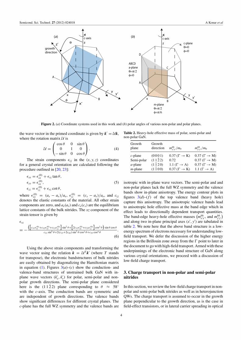
The above Hamiltonians are constructed using acoordinate system (x, y, z) suitable for describing c-planegrowth as shown in figure 2(a). To describe the bands in non-c-plane nitrides, one needs to rotate the coordinate system andgo from the unprimed to the primed coordinates (x*, y*, z*)[20–22] as shown in figure 2. We rotate the coordinate systemin such a way that z* points along the growth direction. Withsuch a condition, any non-polar or semi-polar plane can bedescribed by two rotation angles ' and (, respectively. Forexample, for the c-plane, ' = 0 and ( = 0. For the a-plane,' = )/2 and ( = 0, for the m-plane, ' = )/2 and ( = )/6,and so on. In this work, we consider semi-polar and non-polarplanes passing through the line AB (( = 0). For such planes,
3
Semicond. Sci. Technol. 27 (2012) 024018 A Konar et al
z
xy
(a) (b)
y’
#
x’$
A
B
c-axis
z
xy
y’
c-axis
A
B
C
D
ABCDa-plane#="/2$=0
m-plane#="/2$="/6
growthdirection
c-plane#=0$=0
z’
Figure 2. (a) Coordinate systems used in this work and (b) polar angles of various non-polar and polar planes.
the wave vector in the primed coordinate is given by k* = Uk,where the rotation matrix U is
U =
!
#cos ' 0 sin '
0 1 0" sin ' 0 cos '
$
& . (4)
The strain components #i j in the (x, y, z) coordinatesfor a general crystal orientation are calculated following theprocedure outlined in [20, 23]:
#xx = #(0)xx + #xz tan ' ,
#yy = #(0)xx , (5)
#zz = #(0)zz + #xz cot ' ,
where #(0)xx = (as " ae)/ae, #(0)
zz = (cs " as)/ae, and ci j
denotes the elastic constants of the material. All other straincomponents are zero, and ae(as) and ce(cs) are the equilibriumlattice constants of the bulk nitrides. The xz component of thestrain tensor is given by
#xz
= "('
c11#(0)xx +c12#
(0)xx +c13#
(0)zz
*sin2 '+
'2c13#
(0)xx +c33#
(0)zz
*cos2 '
)sin ' cos '
c11 sin4 '+2(c13+2c44) sin2 ' cos2 '+c33 cos4 '.
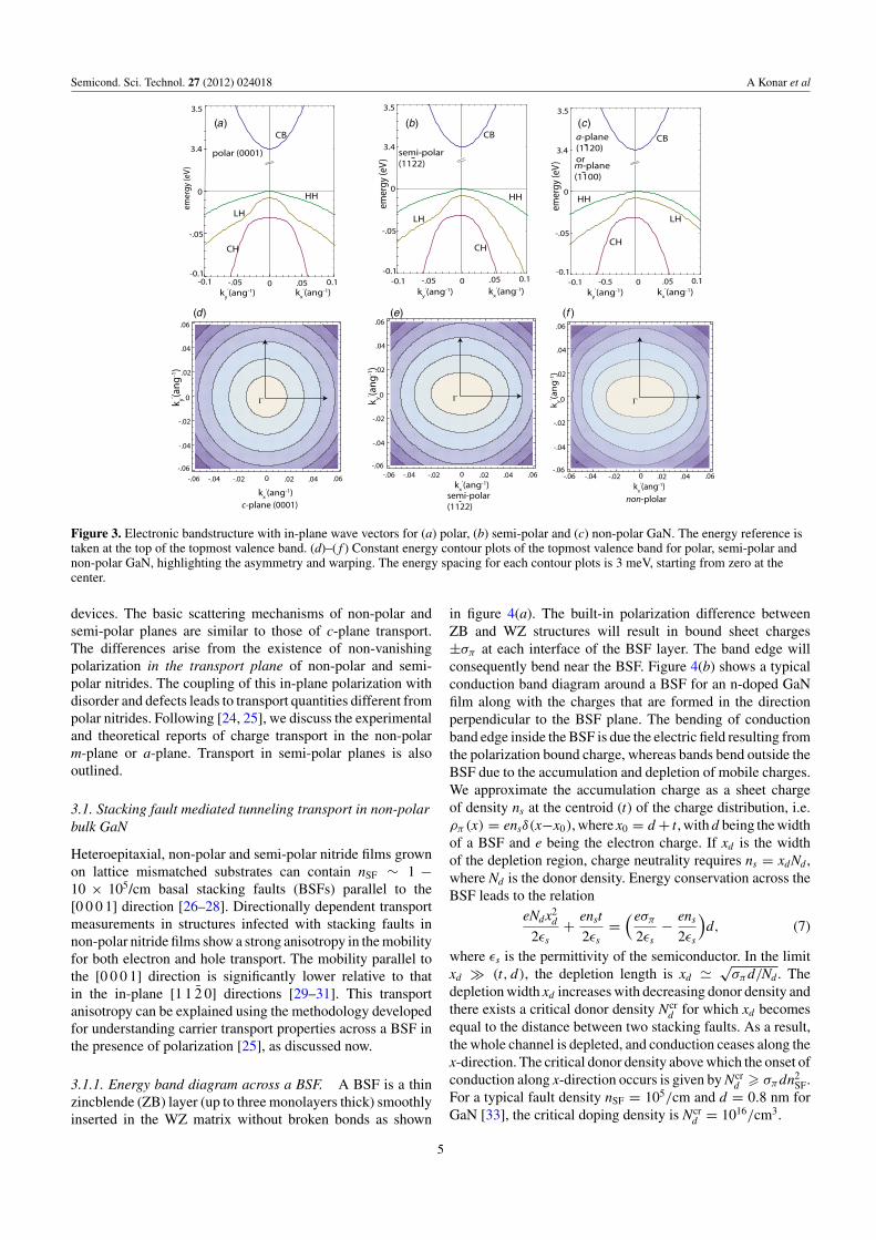
(6)
Using the above strain components and transforming thewave vector using the relation k = UT k* (where T standsfor transpose), the electronic bandstructures of bulk nitridesare easily obtained by diagonalizing the Hamiltonian matrixin equation (1). Figures 3(a)–(c) show the conduction- andvalence-band structures of unstrained bulk GaN with in-plane wave vectors (k*
x, k*y) for polar, semi-polar and non-
polar growth directions. The semi-polar plane consideredhere is the (1 1 2 2) plane corresponding to ' + 58,
with the c-axis. The conduction bands are symmetric andare independent of growth directions. The valence bandsshow significant differences for different crystal planes. Thec-plane has the full WZ symmetry and the valence bands are
Table 2. Heavy-hole effective mass of polar, semi-polar andnon-polar GaN.
Growth Growthplane direction mhh
x*x*/m0 mhhy*y*/m0
c-plane (0 0 0 1) 0.37 (* - K) 0.37 (* - M)Semi-polar (1 1 2 2) 0.72 0.37 (* - M)a-plane (1 1 2 0) 1.1 (* - A) 0.37 (* - M)m-plane (1 1 0 0) 0.37 (* - K) 1.1 (* - A)
isotropic with in-plane wave vectors. The semi-polar and andnon-polar planes lack the full WZ symmetry and the valencebands show in-plane anisotropy. The energy contour plots infigures 3(d)–( f ) of the top valence band (heavy hole)capture this anisotropy. The anisotropic valence bands leadto anisotropic hole effective mass at the band edge which ineffect leads to directionally dependent transport quantities.The band-edge heavy-hole effective masses
(mhh
x*x* , and mhhy*y*
)
and along two in-plane principal axes (x*, y*) are tabulated intable 2. We note here that the above band structure is a low-energy spectrum of electrons necessary for understanding low-field transport. We defer the discussion of the higher energyregions in the Brillouin zone away from the * point to later inthe document to go with high-field transport. Armed with theseunderpinnings of the electronic band structure of GaN alongvarious crystal orientations, we proceed with a discussion oflow-field charge transport.
3. Charge transport in non-polar and semi-polarnitrides
In this section, we review the low-field charge transport in non-polar and semi-polar bulk nitrides as well as in heterojunctionQWs. The charge transport is assumed to occur in the growthplane perpendicular to the growth direction, as is the case infield-effect transistors, or in lateral carrier spreading in optical
4
Semicond. Sci. Technol. 27 (2012) 024018 A Konar et al
0-0.1 -.05 .05 0.1ky
’(ang-1) kx’(ang-1)
-.05
-0.1
3.4
3.5
CB
HH
LH
CH
polar (0001)
0em
ergy
(eV)
-0.1 -.05 0 .05 0.1
ky’(ang-1) kx
’(ang-1)
-0.1
-.05
0
3.4
3.5
CB
HH
LH
CH
emer
gy (e
V)
semi-polar (1122)
(a)
(d) (e) (f )
(b) (c)CB
HH
LH
CH
-0.1 -0.5 0 .05 0.1-0.1
-.05
0
3.4
3.5
emer
gy (e
V)
a-plane (1120)or
ky’(ang-1) kx
’(ang-1)
m-plane (1100)
k y’ (an
g-1
)
kx’(ang-1)
non-plolar
-.06 -.04 -.02 .02 .040 .06-.06
-.04
-.02
0
.02
.04
.06
%
kx’(ang-1)
k y’ (ang
-1)
c-plane (0001)
-.06 -.04 -.02 .02 .040 .06-.06
-.04
-.02
0
.02
.04
.06
kx’(ang-1)
k y’ (ang
-1)
%
semi-polar (1122)
-.06 -.04 -.02 .02 .040 .06-.06
-.04
-.02
0
.02
.04
.06
%
Figure 3. Electronic bandstructure with in-plane wave vectors for (a) polar, (b) semi-polar and (c) non-polar GaN. The energy reference istaken at the top of the topmost valence band. (d)–( f ) Constant energy contour plots of the topmost valence band for polar, semi-polar andnon-polar GaN, highlighting the asymmetry and warping. The energy spacing for each contour plots is 3 meV, starting from zero at thecenter.
devices. The basic scattering mechanisms of non-polar andsemi-polar planes are similar to those of c-plane transport.The differences arise from the existence of non-vanishingpolarization in the transport plane of non-polar and semi-polar nitrides. The coupling of this in-plane polarization withdisorder and defects leads to transport quantities different frompolar nitrides. Following [24, 25], we discuss the experimentaland theoretical reports of charge transport in the non-polarm-plane or a-plane. Transport in semi-polar planes is alsooutlined.
3.1. Stacking fault mediated tunneling transport in non-polarbulk GaN
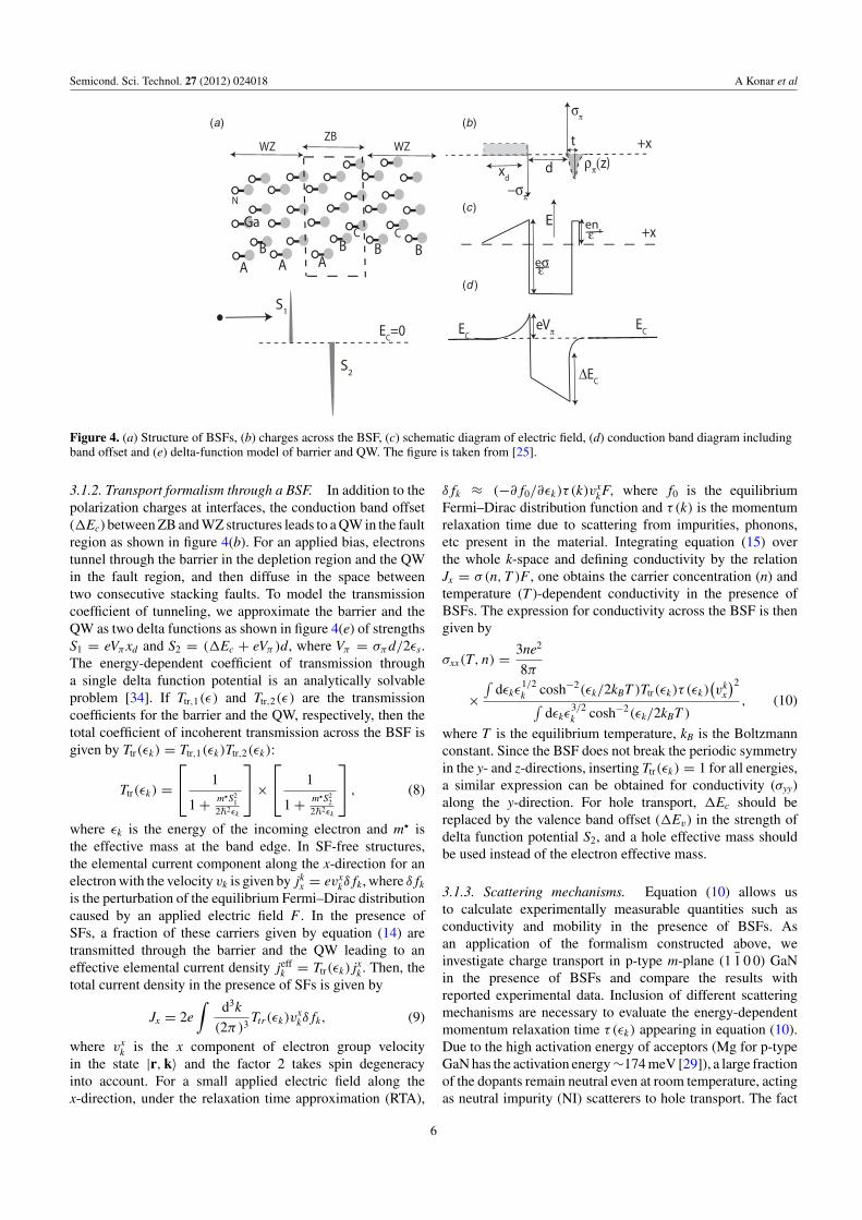
Heteroepitaxial, non-polar and semi-polar nitride films grownon lattice mismatched substrates can contain nSF ! 1 "10 ) 105/cm basal stacking faults (BSFs) parallel to the[0 0 0 1] direction [26–28]. Directionally dependent transportmeasurements in structures infected with stacking faults innon-polar nitride films show a strong anisotropy in the mobilityfor both electron and hole transport. The mobility parallel tothe [0 0 0 1] direction is significantly lower relative to thatin the in-plane [1 1 2 0] directions [29–31]. This transportanisotropy can be explained using the methodology developedfor understanding carrier transport properties across a BSF inthe presence of polarization [25], as discussed now.
3.1.1. Energy band diagram across a BSF. A BSF is a thinzincblende (ZB) layer (up to three monolayers thick) smoothlyinserted in the WZ matrix without broken bonds as shown
in figure 4(a). The built-in polarization difference betweenZB and WZ structures will result in bound sheet charges±+) at each interface of the BSF layer. The band edge willconsequently bend near the BSF. Figure 4(b) shows a typicalconduction band diagram around a BSF for an n-doped GaNfilm along with the charges that are formed in the directionperpendicular to the BSF plane. The bending of conductionband edge inside the BSF is due the electric field resulting fromthe polarization bound charge, whereas bands bend outside theBSF due to the accumulation and depletion of mobile charges.We approximate the accumulation charge as a sheet chargeof density ns at the centroid (t) of the charge distribution, i.e.,) (x) = ens-(x"x0), where x0 = d + t, with d being the widthof a BSF and e being the electron charge. If xd is the widthof the depletion region, charge neutrality requires ns = xdNd ,where Nd is the donor density. Energy conservation across theBSF leads to the relation
eNdx2d
2#s+ enst
2#s=
+e+)
2#s" ens
2#s
,d, (7)
where #s is the permittivity of the semiconductor. In the limitxd . (t, d), the depletion length is xd /
&+)d/Nd . The
depletion width xd increases with decreasing donor density andthere exists a critical donor density Ncr
d for which xd becomesequal to the distance between two stacking faults. As a result,the whole channel is depleted, and conduction ceases along thex-direction. The critical donor density above which the onset ofconduction along x-direction occurs is given by Ncr
d ! +)dn2SF.
For a typical fault density nSF = 105/cm and d = 0.8 nm forGaN [33], the critical doping density is Ncr
d = 1016/cm3.
5
Semicond. Sci. Technol. 27 (2012) 024018 A Konar et al
AB
A AB
C CB B
WZZB
WZ
Ga
N
(a) (b)
(c)
(d )
xd
+x
&!"
!"
d
ECECeV"
'EC
t
("(z)
e! )
ens )E
+x
EC=0
S1
S2
Figure 4. (a) Structure of BSFs, (b) charges across the BSF, (c) schematic diagram of electric field, (d) conduction band diagram includingband offset and (e) delta-function model of barrier and QW. The figure is taken from [25].
3.1.2. Transport formalism through a BSF. In addition to thepolarization charges at interfaces, the conduction band offset("Ec) between ZB and WZ structures leads to a QW in the faultregion as shown in figure 4(b). For an applied bias, electronstunnel through the barrier in the depletion region and the QWin the fault region, and then diffuse in the space betweentwo consecutive stacking faults. To model the transmissioncoefficient of tunneling, we approximate the barrier and theQW as two delta functions as shown in figure 4(e) of strengthsS1 = eV)xd and S2 = ("Ec + eV) )d, where V) = +)d/2#s.The energy-dependent coefficient of transmission througha single delta function potential is an analytically solvableproblem [34]. If Ttr,1(#) and Ttr,2(#) are the transmissioncoefficients for the barrier and the QW, respectively, then thetotal coefficient of incoherent transmission across the BSF isgiven by Ttr(#k) = Ttr,1(#k)Ttr,2(#k):
Ttr(#k) =
-
. 1
1 + m!S21
2!2#k
/
0 )
-
. 1
1 + m!S22
2!2#k
/
0 , (8)
where #k is the energy of the incoming electron and m! isthe effective mass at the band edge. In SF-free structures,the elemental current component along the x-direction for anelectron with the velocity vk is given by jk
x = evxk- fk, where - fk
is the perturbation of the equilibrium Fermi–Dirac distributioncaused by an applied electric field F . In the presence ofSFs, a fraction of these carriers given by equation (14) aretransmitted through the barrier and the QW leading to aneffective elemental current density jeff
k = Ttr(#k) jxk . Then, the
total current density in the presence of SFs is given by
Jx = 2e1
d3k(2) )3
Ttr(#k)vxk- fk, (9)
where vxk is the x component of electron group velocity
in the state |r, k% and the factor 2 takes spin degeneracyinto account. For a small applied electric field along thex-direction, under the relaxation time approximation (RTA),
- fk + (". f0/.#k)/ (k)vxkF, where f0 is the equilibrium
Fermi–Dirac distribution function and / (k) is the momentumrelaxation time due to scattering from impurities, phonons,etc present in the material. Integrating equation (15) overthe whole k-space and defining conductivity by the relationJx = + (n, T )F , one obtains the carrier concentration (n) andtemperature (T )-dependent conductivity in the presence ofBSFs. The expression for conductivity across the BSF is thengiven by
+xx(T, n) = 3ne2
8)
)2
d#k#1/2k cosh"2(#k/2kBT )Ttr(#k)/ (#k)
(vk
x
)2
2d#k#
3/2k cosh"2(#k/2kBT )
, (10)
where T is the equilibrium temperature, kB is the Boltzmannconstant. Since the BSF does not break the periodic symmetryin the y- and z-directions, inserting Ttr(#k) = 1 for all energies,a similar expression can be obtained for conductivity (+yy)along the y-direction. For hole transport, "Ec should bereplaced by the valence band offset ("Ev) in the strength ofdelta function potential S2, and a hole effective mass shouldbe used instead of the electron effective mass.
3.1.3. Scattering mechanisms. Equation (10) allows usto calculate experimentally measurable quantities such asconductivity and mobility in the presence of BSFs. Asan application of the formalism constructed above, weinvestigate charge transport in p-type m-plane (1 1 0 0) GaNin the presence of BSFs and compare the results withreported experimental data. Inclusion of different scatteringmechanisms are necessary to evaluate the energy-dependentmomentum relaxation time / (#k) appearing in equation (10).Due to the high activation energy of acceptors (Mg for p-typeGaN has the activation energy !174 meV [29]), a large fractionof the dopants remain neutral even at room temperature, actingas neutral impurity (NI) scatterers to hole transport. The fact
6
Semicond. Sci. Technol. 27 (2012) 024018 A Konar et al
p-doped GaN film
0 1 2 3 4 5 0
1
2
3
5
4
carrier density p (x 1018/cm3)
film
con
duct
ivit
y (o
hm-1
cm-1
)
theoryexp
!xx
!yy
GaNBSF
M-plane
x
yz
0 1 2 3 4 5
5
15
25
30
drift
mob
ility
(cm
2 /v.s
)
GaNBSF
M-plane
carrier density p (x 1018/cm3)
BSF-limited anisotropy
theoryexp
µxx
µyyx
yz
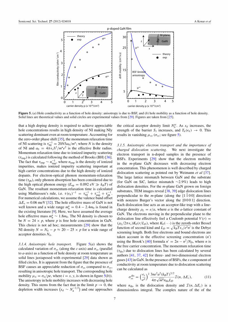
Figure 5. (a) Hole conductivity as a function of hole density: anisotropy is due to BSF, and (b) hole mobility as a function of hole density.Solid lines are theoretical values and solid circles are experimental values from [29]. Figures are taken from [25].
that a high doping density is required to achieve appreciablehole concentrations results in high density of NI making NIyscattering dominant even at room temperature. Accounting forthe zero-order phase shift [35], the momentum relaxation timeof NI scattering is /"1
NI = 20N!a0/m!; where N is the densityof NI and a0 = 4)#s!2/m!e2 is the effective Bohr radius.Momentum relaxation time due to ionized impurity scattering(/imp) is calculated following the method of Brooks (BH) [36].The fact that /imp ! n"1
imp, where nimp is the density of ionizedimpurities, makes ionized impurity scattering important athigh carrier concentrations due to the high density of ionizeddopants. For electron-optical phonon momentum-relaxationtime (/ph), only phonon absorption has been considered due tothe high optical phonon energy (Eop = 0.092 eV . kBT ) ofGaN. The resultant momentum-relaxation time is calculatedusing Mathiessen’s rule, i.e. / (#k)
"1 = /"1NI + /"1
imp + /"1ph .
For numerical calculations, we assume the valence band offset"Ev = 0.06 meV [32]. The hole effective mass of GaN is notwell known and a wide range m!
h = 0.4 " 2.4m0 is found inthe existing literature [9]. Here, we have assumed the averagehole effective mass m!
h ! 1.8m0. The NI density is chosen tobe N = 24 ) p, where p is free hole concentration in GaN.This choice is not ad hoc; measurements [29] show that theNI density N = NA " p + 20 " 25 ) p for a wide range ofacceptor densities NA.
3.1.4. Anisotropic hole transport. Figure 5(a) shows thecalculated variation of +xx (along the c-axis) and +yy (parallelto a-axis) as a function of hole density at room temperature assolid lines juxtaposed with experimental [29] data shown asfilled circles. It is apparent from the figure that the presence ofBSF causes an appreciable reduction of +xx compared to +yy,resulting in anisotropic hole transport. The corresponding holemobility µii = +ii/pe, where i = x, y, is shown in figure 5(b)).The anisotropy in hole mobility increases with decreasing holedensity. This stems from the fact that in the limit p - 0, thedepletion width increases
(xd ! N"1/2
A
)and one approaches
the critical acceptor density limit NcrA . As xd increases, the
strength of the barrier S1 increases, and Ttr(#k) - 0. Thisresults in vanishing µxx (+xx; see figure 5).
3.1.5. Anisotropic electron transport and the importance ofcharged dislocation scattering. We next investigate theelectron transport in n-doped samples in the presence ofBSFs. Experiments [29] show that the electron mobilityin the m-plane GaN decreases with decreasing electronconcentration. This phenomenon is well described by chargeddislocation scattering as pointed out by Weimann et al [37].The large lattice mismatch between GaN and the substrate(for GaN on SiC, lattice mismatch !2.9%) leads to highdislocation densities. For the m-plane GaN grown on foreignsubstrates, TEM images reveal [38, 39] edge dislocation linesperpendicular to the m-plane (along the [1 1 0 0] direction)with nonzero Burger’s vector along the [0 0 0 1] direction.Each dislocation line acts as an acceptor-like trap with a line-charge density ,L = e/a, where a is the a-lattice constant ofGaN. The electrons moving in the perpendicular plane to thedislocation line effectively feel a Coulomb potential V (r) =(,L/2)#s)K0(r/LD), where K0(· · ·) is the zeroth-order Besselfunction of second kind and LD =
3kBT#s/e2n* is the Debye
screening length. Both free electrons and bound electrons aretaken account in the effective screening concentration (n*)using the Brook’s [40] formula n* = 2n " n2/ND, where n isthe free carrier concentration. The momentum relaxation time(/dis) due to dislocation lines has been calculated by severalauthors [41, 37, 42] for three- and two-dimensional electrongases [43] in GaN. In the presence of BSFs, the x component ofconductivity at room temperature due to dislocation scatteringcan be calculated as
+ disxx =
+ #s
e2
,2 3ne2a2(kBT )3/2
4)&
m!ndisLDI(n,"Ec), (11)
where ndis is the dislocation density and I(n,"Ec) is adimensionless integral. The complex nature of the of the
7
Semicond. Sci. Technol. 27 (2012) 024018 A Konar et al
0.1 0.2 0.5 1 2 4
carrier density n (x 1018/cm3)
drift
mob
ility
(cm
2 /v.s
)
100
150
200
300
GaNBSF
M-planeµxx
µyy
BSF-limited anisotropy
ndis=2x 10⁹/cm2
0.1 0.5 1 2 5 10
100
200
500
700
300
carrier density n (x 1018/cm3)
drift
mob
ility
(cm
2 /v.s
)
GaNBSF
M-plane
theoryexp
n-doped GaN film
x
yz
x
yz
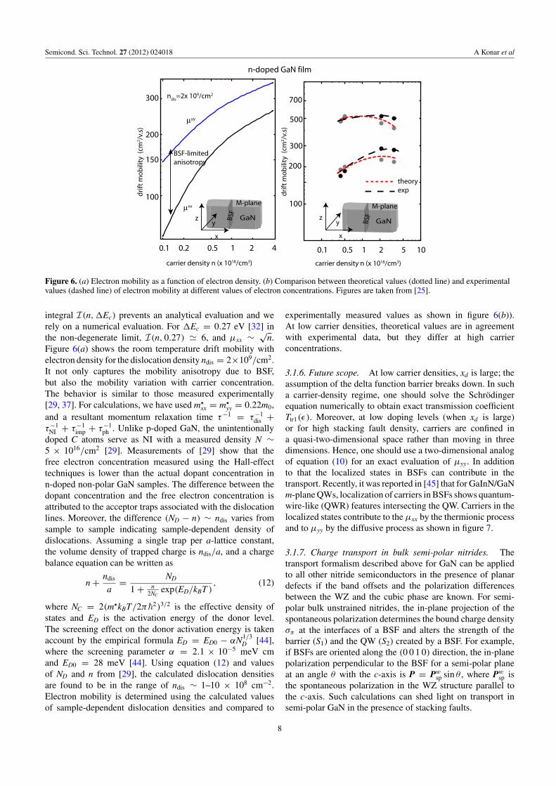
Figure 6. (a) Electron mobility as a function of electron density. (b) Comparison between theoretical values (dotted line) and experimentalvalues (dashed line) of electron mobility at different values of electron concentrations. Figures are taken from [25].
integral I(n,"Ec) prevents an analytical evaluation and werely on a numerical evaluation. For "Ec = 0.27 eV [32] inthe non-degenerate limit, I(n, 0.27) / 6, and µxx !
&n.
Figure 6(a) shows the room temperature drift mobility withelectron density for the dislocation density ndis = 2)109/cm2.It not only captures the mobility anisotropy due to BSF,but also the mobility variation with carrier concentration.The behavior is similar to those measured experimentally[29, 37]. For calculations, we have used m!
xx = m!yy = 0.22m0,
and a resultant momentum relaxation time /"1 = /"1dis +
/"1NI + /"1
imp + /"1ph . Unlike p-doped GaN, the unintentionally
doped C atoms serve as NI with a measured density N !5 ) 1016/cm2 [29]. Measurements of [29] show that thefree electron concentration measured using the Hall-effecttechniques is lower than the actual dopant concentration inn-doped non-polar GaN samples. The difference between thedopant concentration and the free electron concentration isattributed to the acceptor traps associated with the dislocationlines. Moreover, the difference (ND " n) ! ndis varies fromsample to sample indicating sample-dependent density ofdislocations. Assuming a single trap per a-lattice constant,the volume density of trapped charge is ndis/a, and a chargebalance equation can be written as
n + ndis
a= ND
1 + n2NC
exp(ED/kBT ), (12)
where NC = 2(m!kBT/2)!2)3/2 is the effective density ofstates and ED is the activation energy of the donor level.The screening effect on the donor activation energy is takenaccount by the empirical formula ED = ED0 " 0N1/3
D [44],where the screening parameter 0 = 2.1 ) 10"5 meV cmand ED0 = 28 meV [44]. Using equation (12) and valuesof ND and n from [29], the calculated dislocation densitiesare found to be in the range of ndis ! 1–10 ) 108 cm"2.Electron mobility is determined using the calculated valuesof sample-dependent dislocation densities and compared to
experimentally measured values as shown in figure 6(b)).At low carrier densities, theoretical values are in agreementwith experimental data, but they differ at high carrierconcentrations.
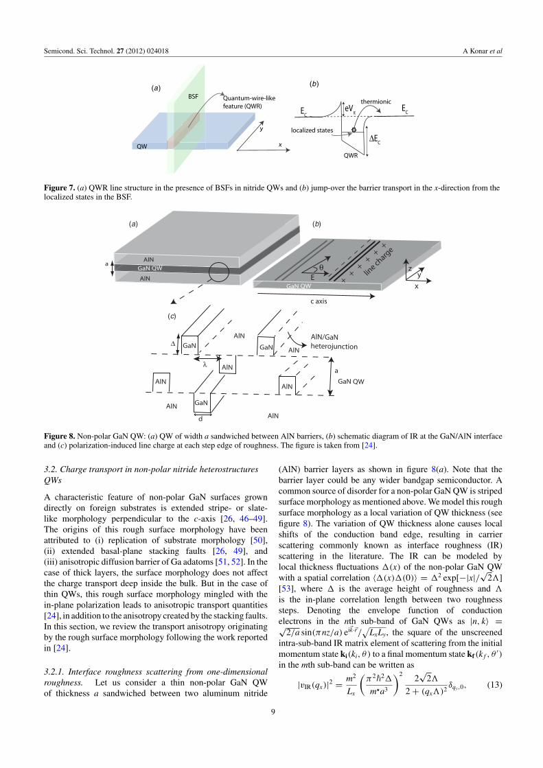
3.1.6. Future scope. At low carrier densities, xd is large; theassumption of the delta function barrier breaks down. In sucha carrier-density regime, one should solve the Schrodingerequation numerically to obtain exact transmission coefficientTtr1(#). Moreover, at low doping levels (when xd is large)or for high stacking fault density, carriers are confined ina quasi-two-dimensional space rather than moving in threedimensions. Hence, one should use a two-dimensional analogof equation (10) for an exact evaluation of µyy. In additionto that the localized states in BSFs can contribute in thetransport. Recently, it was reported in [45] that for GaInN/GaNm-plane QWs, localization of carriers in BSFs shows quantum-wire-like (QWR) features intersecting the QW. Carriers in thelocalized states contribute to the µxx by the thermionic processand to µyy by the diffusive process as shown in figure 7.
3.1.7. Charge transport in bulk semi-polar nitrides. Thetransport formalism described above for GaN can be appliedto all other nitride semiconductors in the presence of planardefects if the band offsets and the polarization differencesbetween the WZ and the cubic phase are known. For semi-polar bulk unstrained nitrides, the in-plane projection of thespontaneous polarization determines the bound charge density+) at the interfaces of a BSF and alters the strength of thebarrier (S1) and the QW (S2) created by a BSF. For example,if BSFs are oriented along the (0 0 1 0) direction, the in-planepolarization perpendicular to the BSF for a semi-polar planeat an angle ' with the c-axis is P = Pw
sp sin ' , where Pwsp is
the spontaneous polarization in the WZ structure parallel tothe c-axis. Such calculations can shed light on transport insemi-polar GaN in the presence of stacking faults.
8
Semicond. Sci. Technol. 27 (2012) 024018 A Konar et al
ECECeV"
'ECQW
BSF Quantum-wire-like feature (QWR)
x
y
thermionic
(a) (b)
localized states
QWR
Figure 7. (a) QWR line structure in the presence of BSFs in nitride QWs and (b) jump-over the barrier transport in the x-direction from thelocalized states in the BSF.
(a) (b)
(c)
AlNGaN QW
AlN
a
GaN QW + +
+ +
+ +
& & & & & & &
line charg
e
c axis
xy
z
GaN QWAlN
AlN
GaN GaN
GaN
*
d
a
'
AlN
AlN
AlN/GaN heterojunction
AlN
AlN
AlN
E#
Figure 8. Non-polar GaN QW: (a) QW of width a sandwiched between AlN barriers, (b) schematic diagram of IR at the GaN/AlN interfaceand (c) polarization-induced line charge at each step edge of roughness. The figure is taken from [24].
3.2. Charge transport in non-polar nitride heterostructuresQWs
A characteristic feature of non-polar GaN surfaces growndirectly on foreign substrates is extended stripe- or slate-like morphology perpendicular to the c-axis [26, 46–49].The origins of this rough surface morphology have beenattributed to (i) replication of substrate morphology [50],(ii) extended basal-plane stacking faults [26, 49], and(iii) anisotropic diffusion barrier of Ga adatoms [51, 52]. In thecase of thick layers, the surface morphology does not affectthe charge transport deep inside the bulk. But in the case ofthin QWs, this rough surface morphology mingled with thein-plane polarization leads to anisotropic transport quantities[24], in addition to the anisotropy created by the stacking faults.In this section, we review the transport anisotropy originatingby the rough surface morphology following the work reportedin [24].
3.2.1. Interface roughness scattering from one-dimensionalroughness. Let us consider a thin non-polar GaN QWof thickness a sandwiched between two aluminum nitride
(AlN) barrier layers as shown in figure 8(a). Note that thebarrier layer could be any wider bandgap semiconductor. Acommon source of disorder for a non-polar GaN QW is stripedsurface morphology as mentioned above. We model this roughsurface morphology as a local variation of QW thickness (seefigure 8). The variation of QW thickness alone causes localshifts of the conduction band edge, resulting in carrierscattering commonly known as interface roughness (IR)scattering in the literature. The IR can be modeled bylocal thickness fluctuations "(x) of the non-polar GaN QWwith a spatial correlation 0"(x)"(0)% = "2 exp["|x|/
&2$]
[53], where " is the average height of roughness and $is the in-plane correlation length between two roughnesssteps. Denoting the envelope function of conductionelectrons in the nth sub-band of GaN QWs as |n, k% =&
2/a sin()nz/a) ei!k·!r/3
LxLy, the square of the unscreenedintra-sub-band IR matrix element of scattering from the initialmomentum state ki(ki, ' ) to a final momentum state kf (k f , '
*)in the mth sub-band can be written as
|vIR(qx)|2 = m2
Lx
4)2!2"
m!a3
52 2&
2$
2 + (qx$)2-qy,0, (13)
9
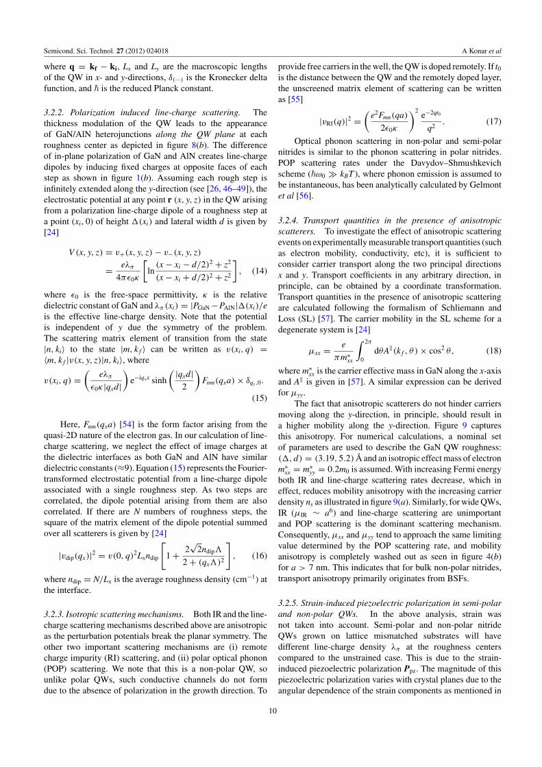
Semicond. Sci. Technol. 27 (2012) 024018 A Konar et al
where q = kf " ki, Lx and Ly are the macroscopic lengthsof the QW in x- and y-directions, -(···) is the Kronecker deltafunction, and ! is the reduced Planck constant.
3.2.2. Polarization induced line-charge scattering. Thethickness modulation of the QW leads to the appearanceof GaN/AlN heterojunctions along the QW plane at eachroughness center as depicted in figure 8(b). The differenceof in-plane polarization of GaN and AlN creates line-chargedipoles by inducing fixed charges at opposite faces of eachstep as shown in figure 1(b). Assuming each rough step isinfinitely extended along the y-direction (see [26, 46–49]), theelectrostatic potential at any point r (x, y, z) in the QW arisingfrom a polarization line-charge dipole of a roughness step ata point (xi, 0) of height "(xi) and lateral width d is given by[24]
V (x, y, z) = v+(x, y, z) " v"(x, y, z)
= e&)
4)#01
6ln
(x " xi " d/2)2 + z2
(x " xi + d/2)2 + z2
7, (14)
where #0 is the free-space permittivity, 1 is the relativedielectric constant of GaN and &) (xi) = |PGaN "PAlN|"(xi)/eis the effective line-charge density. Note that the potentialis independent of y due the symmetry of the problem.The scattering matrix element of transition from the state|n, ki% to the state |m, k f % can be written as v(xi, q) =0m, k f |v(x, y, z)|n, ki%, where
v(xi, q) =4
e&)
#01|qxd|
5e"iqxx sinh
4 |qxd|2
5Fnm(qxa) ) -qy,0.
(15)
Here, Fnm(qxa) [54] is the form factor arising from thequasi-2D nature of the electron gas. In our calculation of line-charge scattering, we neglect the effect of image charges atthe dielectric interfaces as both GaN and AlN have similardielectric constants (+9). Equation (15) represents the Fourier-transformed electrostatic potential from a line-charge dipoleassociated with a single roughness step. As two steps arecorrelated, the dipole potential arising from them are alsocorrelated. If there are N numbers of roughness steps, thesquare of the matrix element of the dipole potential summedover all scatterers is given by [24]
|vdip(qx)|2 = v(0, q)2Lxndip
8
1 +2&
2ndip$
2 + (qx$)2
9
, (16)
where ndip = N/Lx is the average roughness density (cm"1) atthe interface.
3.2.3. Isotropic scattering mechanisms. Both IR and the line-charge scattering mechanisms described above are anisotropicas the perturbation potentials break the planar symmetry. Theother two important scattering mechanisms are (i) remotecharge impurity (RI) scattering, and (ii) polar optical phonon(POP) scattering. We note that this is a non-polar QW, sounlike polar QWs, such conductive channels do not formdue to the absence of polarization in the growth direction. To
provide free carriers in the well, the QW is doped remotely. If t0is the distance between the QW and the remotely doped layer,the unscreened matrix element of scattering can be writtenas [55]
|vRI(q)|2 =4
e2Fmn(qa)
2#01
52 e"2qt0
q2. (17)
Optical phonon scattering in non-polar and semi-polarnitrides is similar to the phonon scattering in polar nitrides.POP scattering rates under the Davydov–Shmushkevichscheme (!20 . kBT ), where phonon emission is assumed tobe instantaneous, has been analytically calculated by Gelmontet al [56].
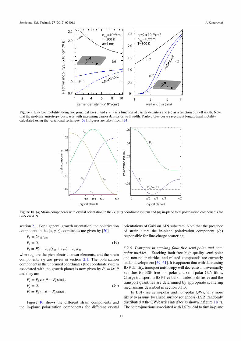
3.2.4. Transport quantities in the presence of anisotropicscatterers. To investigate the effect of anisotropic scatteringevents on experimentally measurable transport quantities (suchas electron mobility, conductivity, etc), it is sufficient toconsider carrier transport along the two principal directionsx and y. Transport coefficients in any arbitrary direction, inprinciple, can be obtained by a coordinate transformation.Transport quantities in the presence of anisotropic scatteringare calculated following the formalism of Schliemann andLoss (SL) [57]. The carrier mobility in the SL scheme for adegenerate system is [24]
µxx = e)m1
xx
1 2)
0d'A#(k f , ' ) ) cos2 ' , (18)
where m1xx is the carrier effective mass in GaN along the x-axis
and A# is given in [57]. A similar expression can be derivedfor µyy.
The fact that anisotropic scatterers do not hinder carriersmoving along the y-direction, in principle, should result ina higher mobility along the y-direction. Figure 9 capturesthis anisotropy. For numerical calculations, a nominal setof parameters are used to describe the GaN QW roughness:(", d) = (3.19, 5.2) A and an isotropic effect mass of electronm1
xx = m1yy = 0.2m0 is assumed. With increasing Fermi energy
both IR and line-charge scattering rates decrease, which ineffect, reduces mobility anisotropy with the increasing carrierdensity ns as illustrated in figure 9(a). Similarly, for wide QWs,IR (µIR ! a6) and line-charge scattering are unimportantand POP scattering is the dominant scattering mechanism.Consequently, µxx and µyy tend to approach the same limitingvalue determined by the POP scattering rate, and mobilityanisotropy is completely washed out as seen in figure 4(b)for a > 7 nm. This indicates that for bulk non-polar nitrides,transport anisotropy primarily originates from BSFs.
3.2.5. Strain-induced piezoelectric polarization in semi-polarand non-polar QWs. In the above analysis, strain wasnot taken into account. Semi-polar and non-polar nitrideQWs grown on lattice mismatched substrates will havedifferent line-charge density &) at the roughness centerscompared to the unstrained case. This is due to the strain-induced piezoelectric polarization Ppz. The magnitude of thispiezoelectric polarization varies with crystal planes due to theangular dependence of the strain components as mentioned in
10
Semicond. Sci. Technol. 27 (2012) 024018 A Konar et al
carrier density n (x1012/cm2)
elec
tro
n m
ob
ility
µ (x
103 c
m2 /V
.s)
ndip=106/cmT=300 Ka=4 nm
1 2 4 6 8 100.7
1.0
1.5
2.0
2.2
µyy
µxx
(a) (b)xy
xy
1 3 5 7well width a (nm)
ns=2 x 10¹²/cm2
ndip=106/cmT=300 K
1.0
0
2.0
2.5
0.5
1.5
µxx
µyy
variational
varia
tiona
l
Figure 9. Electron mobility along two principal axes x and y: (a) as a function of carrier densities and (b) as a function of well width. Notethat the mobility anisotropy decreases with increasing carrier density or well width. Dashed blue curves represent longitudinal mobilitycalculated using the variational technique [58]. Figures are taken from [24].
stra
in c
omp
onen
ts
0
-.01
.01
.02
-.02
crystal plane #0 "/6 "/4 "/3 "/2
)yy
)zz
)xz
)xx
crystal plane #
0 "/6 "/4 "/3 "/2
Pola
rizat
ion
P (C
/m2 )
.06
.04
.02
0
-.02Px’
Pz’
Pspw=-.03
Figure 10. (a) Strain components with crystal orientation in the (x, y, z) coordinate system and (b) in-plane total polarization components forGaN on AlN.
section 2.1. For a general growth orientation, the polarizationcomponent in the (x, y, z) coordinates are given by [20]
Px = 2e15#xz,
Py = 0, (19)
Pz = Pwsp + e31(#xx + #yy) + e33#zz,
where ei j are the piezoelectric tensor elements, and the straincomponents #i j are given in section 2.1. The polarizationcomponent in the unprimed coordinates (the coordinate systemassociated with the growth plane) is now given by P* = UT Pand they are
P*x = Px cos ' " Pz sin ' ,
P*y = 0, (20)
P*z = Px sin ' + Pz cos ' .
Figure 10 shows the different strain components andthe in-plane polarization components for different crystal
orientations of GaN on AlN substrate. Note that the presenceof strain alters the in-plane polarization component (P*
x)responsible for line-charge scattering.
3.2.6. Transport in stacking fault-free semi-polar and non-polar nitrides. Stacking fault-free high-quality semi-polarand non-polar nitrides and related compounds are currentlyunder development [59–61]. It is apparent that with decreasingBSF density, transport anisotropy will decrease and eventuallyvanishes for BSF-free non-polar and semi-polar GaN films.Charge transport in BSF-free bulk nitrides is diffusive and thetransport quantities are determined by appropriate scatteringmechanisms described in section 3.1.3.
In BSF-free semi-polar and non-polar QWs, it is morelikely to assume localized surface roughness (LSR) randomlydistributed at the QW/barrier interface as shown in figure 11(a).The heterojunctions associated with LSRs lead to tiny in-plane
11
Semicond. Sci. Technol. 27 (2012) 024018 A Konar et al
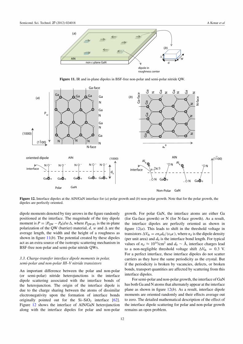
dW
'
non c-plane GaN
dipole inroughness center
AlN
(a)
(b)
Figure 11. IR and in-plane dipoles in BSF-free non-polar and semi-polar nitride QW.
Ga
N
Ga
N
Ga
Ga
N
N
Ga Ga Ga
N N N
Psp
(1000)
(1100)
Ga-face
N-face
+
-N
Ga +
-N
Ga +
-N
Ga +
-N
Ga +
-N
Ga
AlN
GaN
interface
(1000)
Polar
Ga
N Ga
N Ga
GaN N
Ga
Ga
Ga
NN
N
P sp
Ga-
face
N-f
ace
+
- N
Ga
AlN
GaN
interface
Non-Polar
+
- NAl
(1100)
+
- NAl
+
- N
Ga
2"/3
oriented dipole
(a) (b)
d0
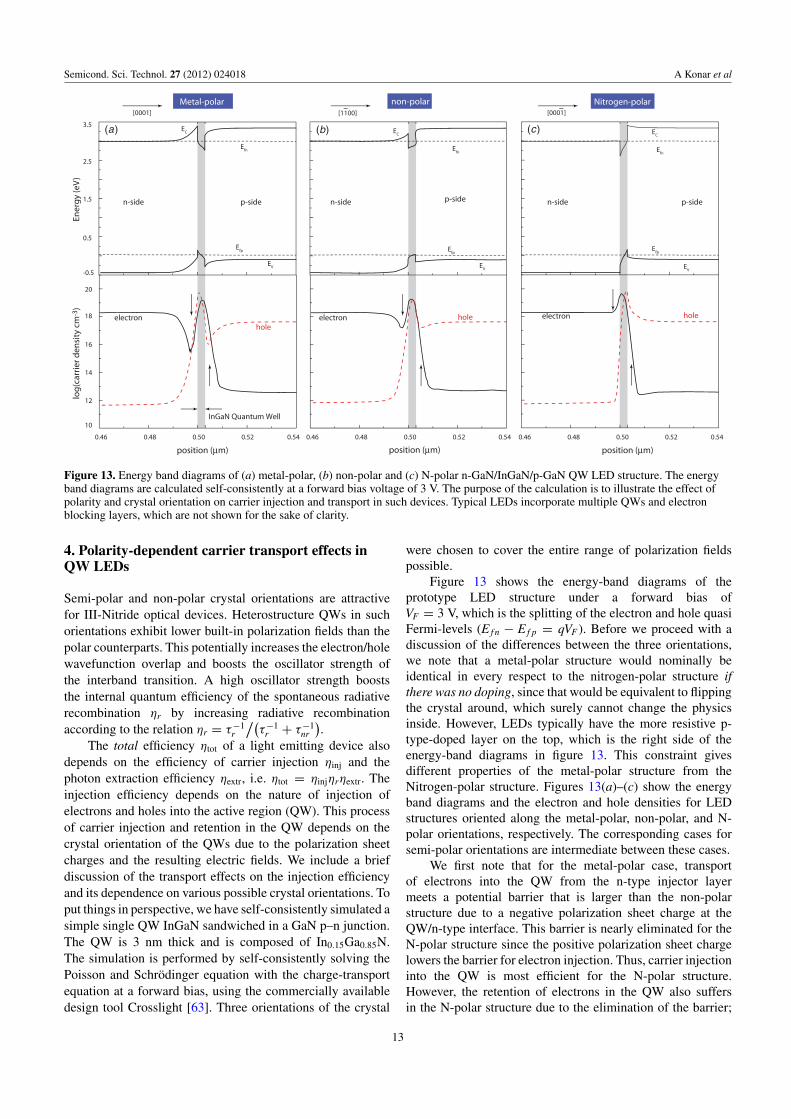
Figure 12. Interface dipoles at the AlN/GaN interface for (a) polar growth and (b) non-polar growth. Note that for the polar growth, thedipoles are perfectly oriented.
dipole moments denoted by tiny arrows in the figure randomlypositioned at the interface. The magnitude of the tiny dipolemoment is P = |PQW " PB|dw", where PQW(B) is the in-planepolarization of the QW (barrier) material, d, w and " are theaverage length, the width and the height of a roughness asshown in figure 11(b). The potential created by these dipolesact as an extra source of the isotropic scattering mechanism inBSF-free non-polar and semi-polar nitride QWs.
3.3. Charge-transfer interface dipole moments in polar,semi-polar and non-polar III–V nitride transistors
An important difference between the polar and non-polar(or semi-polar) nitride heterojunctions is the interfacedipole scattering associated with the interface bonds ofthe heterojunction. The origin of the interface dipole isdue to the charge sharing between the atoms of dissimilarelectronegativity upon the formation of interface bondsoriginally pointed out for the Si–SiO2 interface [62].Figure 12 shows the interface of AlN/GaN heterojunctionalong with the interface dipoles for polar and non-polar
growth. For polar GaN, the interface atoms are either Ga(for Ga-face growth) or N (for N-face growth). As a result,the interface dipoles are perfectly oriented as shown infigure 12(a). This leads to shift in the threshold voltage intransistors "Vth = endd0/(#01 ), where nd is the dipole density(per unit area) and d0 is the interface bond length. For typicalvalues of nd + 1014/cm2 and d0 ! A, interface charges leadto a non-negligible threshold voltage shift "Vth = 0.3 V.For a perfect interface, these interface dipoles do not scattercarriers as they have the same periodicity as the crystal. Butif the periodicity is broken by vacancies, defects, or brokenbonds, transport quantities are affected by scattering from thisinterface dipoles.
For semi-polar and non-polar growth, the interface of GaNhas both Ga and N atoms that alternately appear at the interfaceplane as shown in figure 12(b). As a result, interface dipolemoments are oriented randomly and their effects average outto zero. The detailed mathematical description of the effect ofthe interface dipole scattering for polar and non-polar growthremains an open problem.
12
Semicond. Sci. Technol. 27 (2012) 024018 A Konar et al
-0.5
0.5
1.5
2.5
3.5
Ener
gy (e
V)
n-side p-side
Efp
Efn
EC
EV
0.46 0.48 0.50 0.52 0.54
position (µm)
10
12
14
16
18
20
log(
carr
ier d
ensi
ty c
m-3
)
electron hole
InGaN Quantum Well
Metal-polar [0001]
n-side p-side
Efp
Efn
EC
EV
0.46 0.48 0.50 0.52 0.54
electron hole
[1100]
n-side p-side
Efp
Efn
EC
EV
0.46 0.48 0.50 0.52 0.54
electron hole
Nitrogen-polar [0001]
non-polar
position (µm) position (µm)
(a) (b) (c)
Figure 13. Energy band diagrams of (a) metal-polar, (b) non-polar and (c) N-polar n-GaN/InGaN/p-GaN QW LED structure. The energyband diagrams are calculated self-consistently at a forward bias voltage of 3 V. The purpose of the calculation is to illustrate the effect ofpolarity and crystal orientation on carrier injection and transport in such devices. Typical LEDs incorporate multiple QWs and electronblocking layers, which are not shown for the sake of clarity.
4. Polarity-dependent carrier transport effects inQW LEDs
Semi-polar and non-polar crystal orientations are attractivefor III-Nitride optical devices. Heterostructure QWs in suchorientations exhibit lower built-in polarization fields than thepolar counterparts. This potentially increases the electron/holewavefunction overlap and boosts the oscillator strength ofthe interband transition. A high oscillator strength booststhe internal quantum efficiency of the spontaneous radiativerecombination 3r by increasing radiative recombinationaccording to the relation 3r = /"1
r
:(/"1
r + /"1nr
).
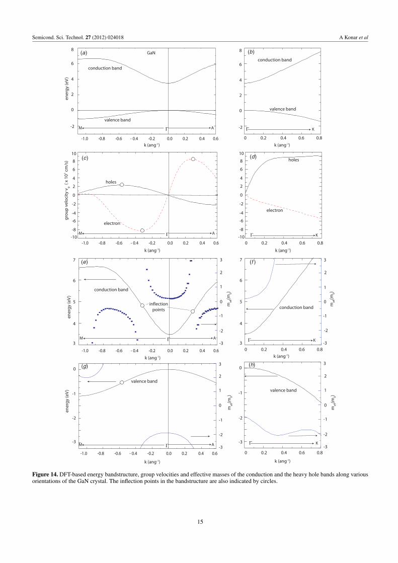
The total efficiency 3tot of a light emitting device alsodepends on the efficiency of carrier injection 3inj and thephoton extraction efficiency 3extr, i.e. 3tot = 3inj3r3extr. Theinjection efficiency depends on the nature of injection ofelectrons and holes into the active region (QW). This processof carrier injection and retention in the QW depends on thecrystal orientation of the QWs due to the polarization sheetcharges and the resulting electric fields. We include a briefdiscussion of the transport effects on the injection efficiencyand its dependence on various possible crystal orientations. Toput things in perspective, we have self-consistently simulated asimple single QW InGaN sandwiched in a GaN p–n junction.The QW is 3 nm thick and is composed of In0.15Ga0.85N.The simulation is performed by self-consistently solving thePoisson and Schrodinger equation with the charge-transportequation at a forward bias, using the commercially availabledesign tool Crosslight [63]. Three orientations of the crystal
were chosen to cover the entire range of polarization fieldspossible.
Figure 13 shows the energy-band diagrams of theprototype LED structure under a forward bias ofVF = 3 V, which is the splitting of the electron and hole quasiFermi-levels (E f n " E f p = qVF ). Before we proceed with adiscussion of the differences between the three orientations,we note that a metal-polar structure would nominally beidentical in every respect to the nitrogen-polar structure ifthere was no doping, since that would be equivalent to flippingthe crystal around, which surely cannot change the physicsinside. However, LEDs typically have the more resistive p-type-doped layer on the top, which is the right side of theenergy-band diagrams in figure 13. This constraint givesdifferent properties of the metal-polar structure from theNitrogen-polar structure. Figures 13(a)–(c) show the energyband diagrams and the electron and hole densities for LEDstructures oriented along the metal-polar, non-polar, and N-polar orientations, respectively. The corresponding cases forsemi-polar orientations are intermediate between these cases.
We first note that for the metal-polar case, transportof electrons into the QW from the n-type injector layermeets a potential barrier that is larger than the non-polarstructure due to a negative polarization sheet charge at theQW/n-type interface. This barrier is nearly eliminated for theN-polar structure since the positive polarization sheet chargelowers the barrier for electron injection. Thus, carrier injectioninto the QW is most efficient for the N-polar structure.However, the retention of electrons in the QW also suffersin the N-polar structure due to the elimination of the barrier;
13

Semicond. Sci. Technol. 27 (2012) 024018 A Konar et al
electrons can leak back into the n-injector region, causingweaker confinement. Carriers outside the active regions leadto loss, since even if they lead to the interband radiativerecombination, the photons emitted are not at the desiredwavelength. Similarly, electron-wavefunction ‘leakage’ intothe p-layers is successively lowered as one moves from metal-polar through non-polar to N-polar structures. The arrows pointto the effect of the net steady-state carrier densities for the threestructures. Exactly same arguments apply to holes.
For the carriers that are retained, the electron–hole overlapin the active region is the best for the non-polar structure due tothe absence of the polarization field. The cases of metal versusN-polar QWs are worth further discussion under high currentinjection (which is associated with ‘efficiency droop’ observedin LEDs). For both the metal-polar and N-polar structures,the dipole formed by the electrons and holes in the QW isopposite in direction to the polarization charge sheet dipoleat the QW/clad layer interfaces. For the non-polar structure,there is almost no such dipole. As the current injection isincreased, the carrier dipoles increase in strength. For bothpolar QWs, the injected dipole tries to screen the polarizationdipole, which will lead to a better overlap, low spectral shiftand, thus, more efficient radiative recombination. However,the carrier leakage or ‘overshoot’ across the QW will reducefor the metal-polar structure as current injection increases,whereas it will get worse for the N-polar structure compared tolow current injection situations. When compared against eachother, N-polar structures have low leakage across, and worseleakage to the same side of the QW than metal-polar QWLEDs. In general, from the qualitative arguments, it appearsthat the non-polar structure (or low-polarization semi-polarplanes) offer the best compromises over the polar variants. Themetal-polar and N-polar structures have their relative meritsand demerits. These arguments hold for emitters in the visiblewavelengths.
As one moves to higher bandgaps for UV and deep-UV optical emitters, the situation changes due the problemin doping. Due to difficulty in p-type (and to an extentalso n-type) doping of high Al-containing AlGaN layers,the carrier-injection problem dominates the performance ofthe device. The N-polar orientation can help improving thecarrier-injection process by using the polarization charges toeffectively ‘pull’ in carriers into the active regions. In addition,one can use polarization-induced doping techniques in gradedAlGaN structures for further boosting the performance[64–66].
5. High-field transport in semi-polar and non-polarGaN
At high electric fields, electrons gain enough kinetic energyto populate high-energy states of the energy bandstructure.Thus, crystal orientation effects play a major role in high-field or hot-electron transport properties. Such high fieldsoccur in HEMTs in the channel near the drain side of thegate at high drain voltages. In optoelectronic devices designedfor photon emission (LEDs, lasers), the fields are typicallysmall in forward bias regimes and are screened by injected
carriers. However, for photon absorption, devices are typicallyreverse biased, and high electric fields are necessary to sweepphotogenerated carriers out of the absorbing layers before theyrecombine. This phenomenon occurs in UV photodetectors orin avalanche photodiodes (APDs). It is necessary to understandcarrier transport properties along various orientations of theGaN crystal for such devices. To do so, an accurate energybandstructure of GaN is essential.
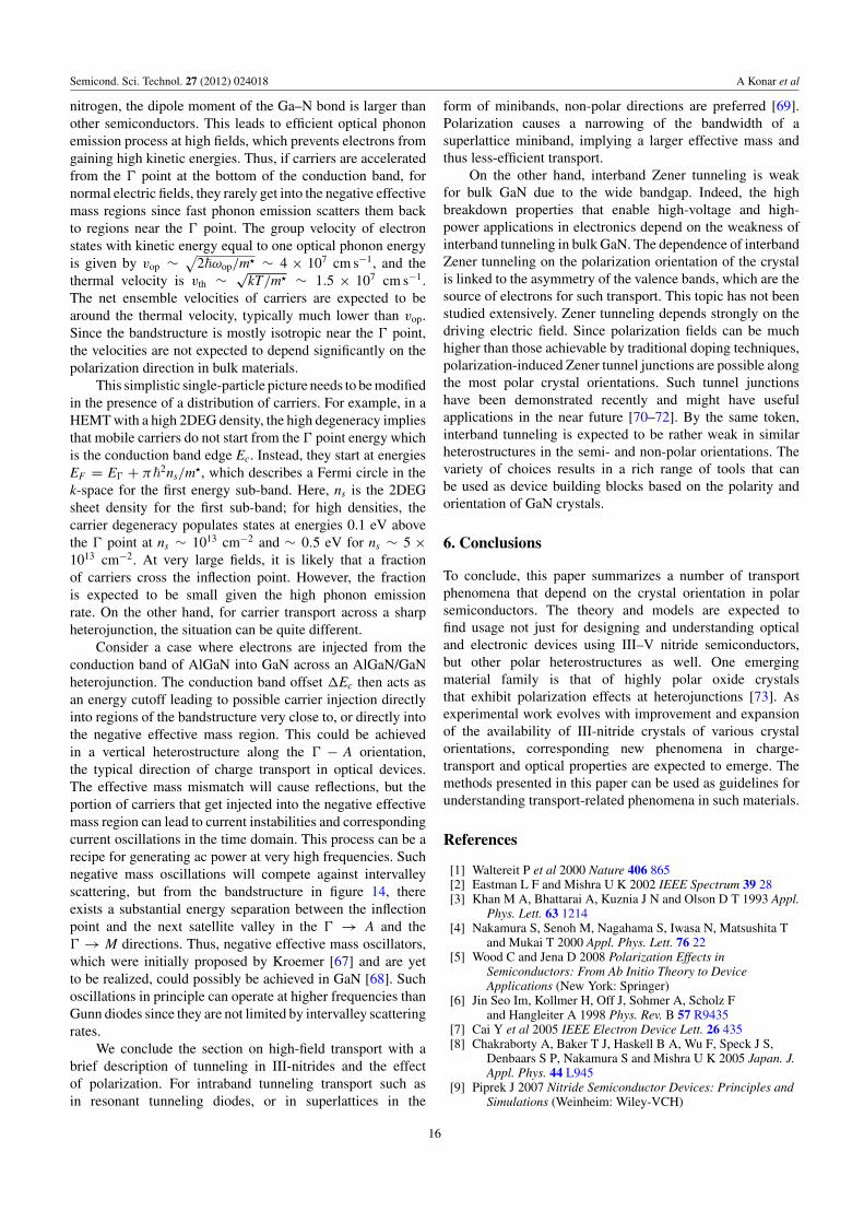
Figure 14 shows the calculated energy bandstructure andvarious associated physical quantities along different crystalorientations of GaN. The bandstructures are provided byProfessor C Van de Walle, the University of California, SantaBarbara, CA. The bandstructure is calculated using hybrid-functional DFT that is able to capture the correct bandgapsand has recently been used to explain various peculiaritiesof GaN devices, such as efficiency droop, among others. Ofprimary interest for high-field transport properties are threeorientations: from * - A, which is along the (0 0 0 1) polarorientation of the GaN crystal, the * - M, which is alongthe (1 1 0 0) orientation, and the * - K, which is along the(1 1 2 0) orientation. The * - A direction is polar, whereasthe * - M and the * - K orientation are non-polar.The bandstructure along the semi-polar direction (e.g. along1 1 2 2) is not shown, but arguments similar to the discussionhere should apply, with an intermediate polarization-inducedfield and charges at heterojunctions. To connect to devices, wenote that vertical transport in c-plane metal-polar as well asN-polar optical devices occurs in the * - A direction nearthe active regions. In access regions from side-contacts (e.g.in etched lateral n-type contacts), the transport is primarily inthe non-polar * - M and * - K directions. On the otherhand, for polar III-nitride HEMTs, the crucial part of transportis primarily in the non-polar * - M and * - K directionsin the two-dimensional electron gas channels confined at theAl(InGa)N/GaN heterojunctions.
Figures 14(c) and (d) show the group velocities vg =!"12kE(k) for the electron and the heavy hole bands. Theelectron group velocity along the * - A and the * - Morientations look similar, reaching the maxima of vmax
g !8 ) 107 cm s"1 at wave vectors k0 ! 0.3 ) 1010 m"1. Theseinflection points in the bandstructure are indicated by opencircles in figure 14(e). They occur at ! 1.1 eV above theconduction band edge in the * - A direction, and at !1.5 eVabove the conduction band edge in the * - M direction. Atthe inflection point, the effective mass of carriers diverges,and at higher energies, it becomes negative. We note thatthe negative effective mass regions exist for the conductionband in the * - A and * - M directions, but not alongthe * - K direction. The electron group velocity along the* - K direction is also lower than the other orientationsat high energies. For the valence band shown, there is aninflection point in the * - M direction.
Most of these high-energy states are not accessed innormal device structures under low bias regimes. This isespecially true in GaN due to the very strong electron–POP interaction in the semiconductor. Owing to the lightatomic mass of nitrogen, the optical phonon energy is high(!2op ! 92 meV), and owing to the high electronegativity of
14
Semicond. Sci. Technol. 27 (2012) 024018 A Konar et al
-2
0
2
4
6
8
ener
gy (e
V)
conduction band
valence band
% AM
-1.0 -0.8 -0.6 - 0.4 -0.2 0.0 0.2 0.4 0.6 k (ang-1)
% K
conduction band
valence band
-2
0
2
4
6
8
k (ang-1)
0 0.2 0.4 0.6 0.8
0 0.2 0.4 0.6 0.8
k (ang-1)
holes
electron
% K
-3
-2
-1
0
m(m
0)
% K
0 0.2 0.4 0.6 0.8-3
-1
0
1
3
2
-2
valence band
k (ang-1)
m(m
0)
0 0.2 0.4 0.6 0.83
4
5
6
7
-3
-1
0
1
3
k (ang-1)
% K
conduction band
2
-2
grou
p ve
loci
ty v
g ( x
107
cm/s
)
-10
-6
-2
0
2
6
10
-1.0 -0.8 -0.6 - 0.4 -0.2 0.0 0.2 0.4 0.6
k (ang-1)
electron
holes
% AM
8
4
-4
-8
-10
-6
-2
0
2
6
10
8
4
-4
-8
3
4
5
6
7
ener
gy (e
V)
m(m
0)
k (ang-1)
-3
-1
0
1
3
2
-2
-1.0 -0.8 -0.6 - 0.4 -0.2 0.0 0.2 0.4 0.6
% AM
conduction band
ener
gy (e
V)
-3
-2
-1
0
valence band
-1.0 -0.8 -0.6 - 0.4 -0.2 0.0 0.2 0.4 0.6
k (ang-1)
% AM
m(m
0)
-1
0
1
3
2
-2
-3
GaN
inflection points
(a) (b)
(c) (d)
(e) (f )
(g) (h)
Figure 14. DFT-based energy bandstructure, group velocities and effective masses of the conduction and the heavy hole bands along variousorientations of the GaN crystal. The inflection points in the bandstructure are also indicated by circles.
15
Semicond. Sci. Technol. 27 (2012) 024018 A Konar et al
nitrogen, the dipole moment of the Ga–N bond is larger thanother semiconductors. This leads to efficient optical phononemission process at high fields, which prevents electrons fromgaining high kinetic energies. Thus, if carriers are acceleratedfrom the * point at the bottom of the conduction band, fornormal electric fields, they rarely get into the negative effectivemass regions since fast phonon emission scatters them backto regions near the * point. The group velocity of electronstates with kinetic energy equal to one optical phonon energyis given by vop !
32!2op/m! ! 4 ) 107 cm s"1, and the
thermal velocity is vth !&
kT/m! ! 1.5 ) 107 cm s"1.The net ensemble velocities of carriers are expected to bearound the thermal velocity, typically much lower than vop.Since the bandstructure is mostly isotropic near the * point,the velocities are not expected to depend significantly on thepolarization direction in bulk materials.
This simplistic single-particle picture needs to be modifiedin the presence of a distribution of carriers. For example, in aHEMT with a high 2DEG density, the high degeneracy impliesthat mobile carriers do not start from the * point energy whichis the conduction band edge Ec. Instead, they start at energiesEF = E* + )!2ns/m!, which describes a Fermi circle in thek-space for the first energy sub-band. Here, ns is the 2DEGsheet density for the first sub-band; for high densities, thecarrier degeneracy populates states at energies 0.1 eV abovethe * point at ns ! 1013 cm"2 and ! 0.5 eV for ns ! 5 )1013 cm"2. At very large fields, it is likely that a fractionof carriers cross the inflection point. However, the fractionis expected to be small given the high phonon emissionrate. On the other hand, for carrier transport across a sharpheterojunction, the situation can be quite different.
Consider a case where electrons are injected from theconduction band of AlGaN into GaN across an AlGaN/GaNheterojunction. The conduction band offset "Ec then acts asan energy cutoff leading to possible carrier injection directlyinto regions of the bandstructure very close to, or directly intothe negative effective mass region. This could be achievedin a vertical heterostructure along the * " A orientation,the typical direction of charge transport in optical devices.The effective mass mismatch will cause reflections, but theportion of carriers that get injected into the negative effectivemass region can lead to current instabilities and correspondingcurrent oscillations in the time domain. This process can be arecipe for generating ac power at very high frequencies. Suchnegative mass oscillations will compete against intervalleyscattering, but from the bandstructure in figure 14, thereexists a substantial energy separation between the inflectionpoint and the next satellite valley in the * - A and the* - M directions. Thus, negative effective mass oscillators,which were initially proposed by Kroemer [67] and are yetto be realized, could possibly be achieved in GaN [68]. Suchoscillations in principle can operate at higher frequencies thanGunn diodes since they are not limited by intervalley scatteringrates.
We conclude the section on high-field transport with abrief description of tunneling in III-nitrides and the effectof polarization. For intraband tunneling transport such asin resonant tunneling diodes, or in superlattices in the
form of minibands, non-polar directions are preferred [69].Polarization causes a narrowing of the bandwidth of asuperlattice miniband, implying a larger effective mass andthus less-efficient transport.
On the other hand, interband Zener tunneling is weakfor bulk GaN due to the wide bandgap. Indeed, the highbreakdown properties that enable high-voltage and high-power applications in electronics depend on the weakness ofinterband tunneling in bulk GaN. The dependence of interbandZener tunneling on the polarization orientation of the crystalis linked to the asymmetry of the valence bands, which are thesource of electrons for such transport. This topic has not beenstudied extensively. Zener tunneling depends strongly on thedriving electric field. Since polarization fields can be muchhigher than those achievable by traditional doping techniques,polarization-induced Zener tunnel junctions are possible alongthe most polar crystal orientations. Such tunnel junctionshave been demonstrated recently and might have usefulapplications in the near future [70–72]. By the same token,interband tunneling is expected to be rather weak in similarheterostructures in the semi- and non-polar orientations. Thevariety of choices results in a rich range of tools that canbe used as device building blocks based on the polarity andorientation of GaN crystals.
6. Conclusions
To conclude, this paper summarizes a number of transportphenomena that depend on the crystal orientation in polarsemiconductors. The theory and models are expected tofind usage not just for designing and understanding opticaland electronic devices using III–V nitride semiconductors,but other polar heterostructures as well. One emergingmaterial family is that of highly polar oxide crystalsthat exhibit polarization effects at heterojunctions [73]. Asexperimental work evolves with improvement and expansionof the availability of III-nitride crystals of various crystalorientations, corresponding new phenomena in charge-transport and optical properties are expected to emerge. Themethods presented in this paper can be used as guidelines forunderstanding transport-related phenomena in such materials.
References
[1] Waltereit P et al 2000 Nature 406 865[2] Eastman L F and Mishra U K 2002 IEEE Spectrum 39 28[3] Khan M A, Bhattarai A, Kuznia J N and Olson D T 1993 Appl.
Phys. Lett. 63 1214[4] Nakamura S, Senoh M, Nagahama S, Iwasa N, Matsushita T
and Mukai T 2000 Appl. Phys. Lett. 76 22[5] Wood C and Jena D 2008 Polarization Effects in
Semiconductors: From Ab Initio Theory to DeviceApplications (New York: Springer)
[6] Jin Seo Im, Kollmer H, Off J, Sohmer A, Scholz Fand Hangleiter A 1998 Phys. Rev. B 57 R9435
[7] Cai Y et al 2005 IEEE Electron Device Lett. 26 435[8] Chakraborty A, Baker T J, Haskell B A, Wu F, Speck J S,
Denbaars S P, Nakamura S and Mishra U K 2005 Japan. J.Appl. Phys. 44 L945
[9] Piprek J 2007 Nitride Semiconductor Devices: Principles andSimulations (Weinheim: Wiley-VCH)
16
Semicond. Sci. Technol. 27 (2012) 024018 A Konar et al
[10] Vanfleet R, Simmons J, Maruska H, Hill D, Chou Mand Chai B 2003 Appl. Phys. Lett. 83 1139
[11] Gardner N, Kim J, Wierer J, Shen Y and Krames M 2005Appl. Phys. Lett. 86 111101
[12] Haskell B A, Baker T J, McLaurin M, Wu F, Fini P T,Denbaars S P, Speck J S and Nakamura S 2005 Appl. Phys.Lett. 86 111917
[13] Ng H 2002 Appl. Phys. Lett. 80 4369[14] Baker T J, Haskell B A, Wu F, Fini P T, Speck J S
and Nakamura S 2005 Japan. J. Appl. Phys 44 L920[15] Takeuchi T, Amano H and Akasaki I 2000 Japan. J. Appl.
Phys. 39 413[16] Ghosh S, Waltereit P, Brandt O, Grahn H T and Ploog K H
2002 Phys. Rev. B 65 075202[17] Kane E O 1957 J. Phys. Chem. Solids 1 249[18] Chuang S L and Chuang C S 1996 Phys. Rev. B 54 2491[19] Lowdin P 1951 J. Phys. Chem. 19 1396[20] Park S H and Chuang S L 1999 Phys. Rev. B 59 4725[21] Park S H, Ahn D and Chuang S L 2007 IEEE J. Quantum
Electron. 43 1175[22] Scheibenzuber W G, Schwarz U T, Veprek R G, Witzigmann B
and Hangleiter A 2009 Phys. Rev. B 80 115320[23] Hinckley J M and Singh J 1990 Phys. Rev. B 42 3546[24] Konar A, Fang T, Sun N and Jena D 2010 Phys. Rev.
B 82 193301[25] Konar A, Fang T, Sun N and Jena D 2011 Appl. Phys.
Lett. 98 022109[26] Haskell B A et al 2005 J. Electron. Mater. 34 357[27] Hsiao C et al 2010 J. Appl. Phys. 107 073502[28] Ueno K, Kobayashi A, Ohta J and Fujioka H 2010 Japan. J.
Appl. Phys. 49 060213[29] McLaurin M, Mates T E, Wu F and Speck J S 2006 J. Appl.
Phys. 100 063707[30] McLaurin M and Speck J S 2007 Phys. Status Solidi
(RRL) 1 110[31] Baik K H et al 2010 IEEE. Photon. Technol. Lett. 22 595[32] Stampfl C and Van de Walle C G 1998 Phys. Rev. B
24 R15052[33] Rebane Y T, Shreter Y G and Albrecht M 1997 Phys. Status
Solidi a 164 141[34] Griffiths D J 2005 Introduction to Quantum Mechanics
(Singapore: Pearson Education)[35] Erginsoy C 1950 Phys. Rev. 79 1013[36] Brooks H 1951 Phys. Rev. 83 879[37] Weimann N G and Eastman L F 1998 J. Appl. Phys.
83 3656[38] Lo I et al 2008 Appl. Phys. Lett. 92 202106[39] Zakharov D N and Liliental-Webber Z 2005 Phys. Rev. B
71 235334[40] Seeger K 1999 Semiconductor Physics: An Introduction 7th
edn (New York: Springer) p 173[41] Podor B 1966 Phys. Status Solidi 16 K167[42] Look D C and Sizelove J R 1998 Phys. Rev. Lett. 82 1237
[43] Jena D, Gossard A C and Mishra U K 2000 Appl. Phys.Lett. 76 1707
[44] Look D C et al 1997 Solid State Commun. 102 297[45] Jonen H et al 2011 Appl. Phys. lett. 99 011901[46] Wang H et al 2004 Appl. Phys. Lett. 84 499[47] Chen C Q et al 2002 Appl. Phys. Lett. 81 3194[48] Paskova T et al 2005 J. Cryst. Growth 281 55[49] Hirai A et al 2007 Appl. Phys. Lett. 90 121119[50] Sun Y J et al 2002 J. Appl. Phys. 92 5714[51] Brandt O, Sun Y J, Dweritz L and Ploog K H 2004 Physica
E 23 339[52] Lymperakis L and Neugebauer J 2009 Phys. Rev. B 79 241308[53] Ferry D K and Goodnick S M 1999 Transport in
Nanostructures (New York: Cambridge University Press)[54] Ridley B K 1999 Electrons and Phonons in Semiconductor
Multilayers 1st edn (New York: Cambridge UniversityPress) p 26
[55] Davis J 2006 Physics of Low-Dimensional Semiconductors:An Introduction 6th edn (Cambridge: Cambridge UniversityPress)
[56] Gelmont B L, Shur M and Stroscio M 1995 J. Appl.Phys. 77 657
[57] Schliemann J and Loss D 2003 Phys. Rev. B 68 165311[58] Zheng Y et al 2003 J. Phys. Soc. Japan 72 2568[59] Schmidt M C, Kim K-C, Farrell R M, Feezell D F,
Cohen D A, Saito M, Fujito K, Speck J S, DenBaars S Pand Nakamura S 2007 Japan. J. Appl. Phys. 46 L190
[60] Enya Y et al 2009 Appl. Phys. Express 2 082101[61] Dadgar A, Ravash R, Veit P, Schmidt G, Muller M,
Dempewolf A, Bertram F, Wieneke M, Christen Jand Krost A 2011 Appl. Phys. Lett. 99 021905
[62] Massoud H Z 1988 J. Appl. Phys. 63 2000[63] Crosslight Software Inc., Burnaby, Canada ApSys
http://www.crosslight.com[64] Simon J, Protasenko V, Lian C, Xing H and Jena D 2010
Science 327 60[65] Verma J, Simon J, Protasenko V, Kosel T, Xing H and Jena D
2011 Appl. Phys. Lett. 99 171104[66] Akyol F, Nath D N, Gu E, Park P S and Rajan S 2011 Japan.
J. Appl. Phys. 50 052101[67] Kroemer H 1958 Phys. Rev. 109 1856[68] Ridley B K, Schaff W J and Eastman L F 2005 J. Appl.
Phys. 97 094503[69] Jena D et al 2011 Phys. Status Solidi a 208 1511[70] Grundmann M J and Mishra U K 2007 Phys. Status Solidi
c 4 2830[71] Simon J, Zhang Z, Goodman K, Xing H, Kosel T, Fay P
and Jena D 2009 Phys. Rev. Lett. 103 026801[72] Krishnamoorthy S, Nath D N, Akyol F, Park P S, Esposto M
and Rajan S 2010 Appl. Phys. Lett. 97 203502[73] S-Bhalla G, Bell C, Ravichandran J, Siemons W, Hikita Y,
Salahuddin S, Hebard A F, Hwang H Y and Ramesh R2011 Nat. Phys. 7 80
17
Related Documents