Characterization of Photonic Structures with CST Microwave Studio Stefan Prorok, Jan Hendrik Wülbern, Jan Hampe, Hooi Sing Lee, Al d Pt dM f d Ei h Alexander Petrov and Manfred Eich Hamburg University of Technology, Institute of Optical and Electronic Materials CST UGM 2010 Hamburg University of Technology Institute of Optical and Electronic Materials, Eich Darmstadt

Welcome message from author
This document is posted to help you gain knowledge. Please leave a comment to let me know what you think about it! Share it to your friends and learn new things together.
Transcript
Characterization of Photonic Structures with CST Microwave Studio
Stefan Prorok, Jan Hendrik Wülbern, Jan Hampe, Hooi Sing Lee, Al d P t d M f d Ei hAlexander Petrov and Manfred Eich
Hamburg University of Technology, Institute of Optical and Electronic Materials
CST UGM 2010
p
Hamburg University of Technology Institute of Optical and Electronic Materials, Eich
Darmstadt
1. Overview1. Overview
2. Ring Resonators
3. 3D Photonic Crystals
4. 2D Photonic Crystals
5. Summary5 Su a y
Hamburg University of Technology Institute of Optical and Electronic Materials, Eich2
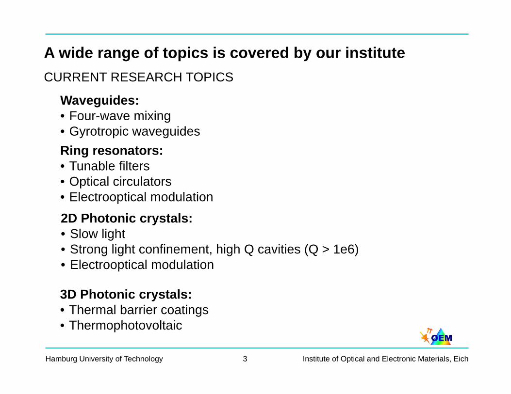
A wide range of topics is covered by our instituteCURRENT RESEARCH TOPICSCURRENT RESEARCH TOPICS
Waveguides:• Four-wave mixing
Ring resonators:• Tunable filters
g• Gyrotropic waveguides
2D Photonic crystals:
• Optical circulators• Electrooptical modulation2D Photonic crystals:• Slow light• Strong light confinement, high Q cavities (Q > 1e6)• Electrooptical modulation
3D Photonic crystals:• Thermal barrier coatings
Th h t lt i
Hamburg University of Technology Institute of Optical and Electronic Materials, Eich3
• Thermophotovoltaic
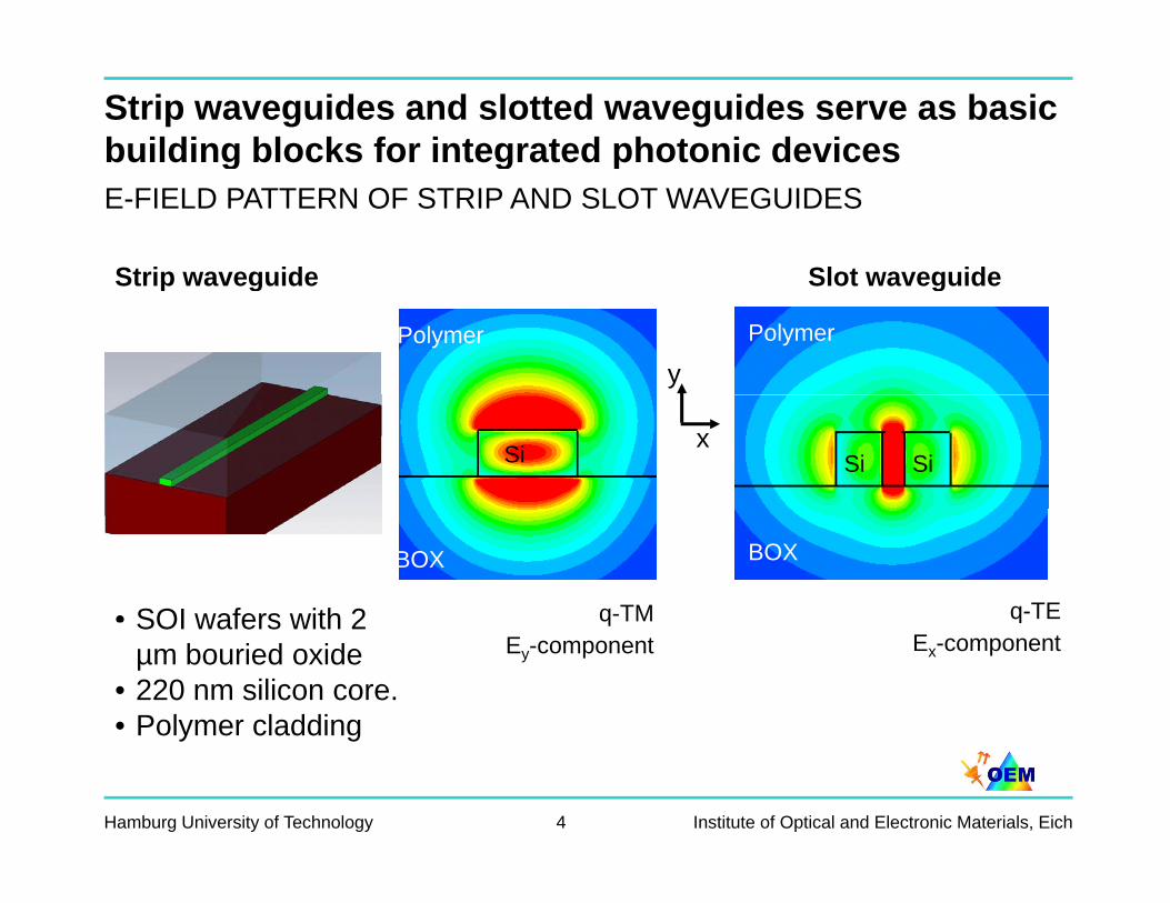
Strip waveguides and slotted waveguides serve as basic building blocks for integrated photonic devicesg g pE-FIELD PATTERN OF STRIP AND SLOT WAVEGUIDES
Strip waveguide Slot waveguide
y
Strip waveguide Slot waveguide
Polymer Polymer
xSi Si Si
q-TM q-TE
BOX BOX
• SOI wafers with 2 qEy-component Ex-component
qSOI wafers with 2 µm bouried oxide
• 220 nm silicon core. • Polymer cladding
Hamburg University of Technology Institute of Optical and Electronic Materials, Eich4
y g
1. Overview1. Overview
2. Ring Resonators
3. 3D Photonic Crystals
4. 2D Photonic Crystals
5. Summary5 Su a y
Hamburg University of Technology Institute of Optical and Electronic Materials, Eich5
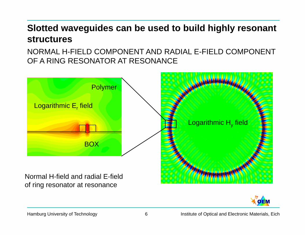
Slotted waveguides can be used to build highly resonant structuresNORMAL H-FIELD COMPONENT AND RADIAL E-FIELD COMPONENT OF A RING RESONATOR AT RESONANCE
Polymer
Logarithmic Hy field
Logarithmic Er field
BOX
Normal H-field and radial E-field of ring resonator at resonance
Hamburg University of Technology Institute of Optical and Electronic Materials, Eich6
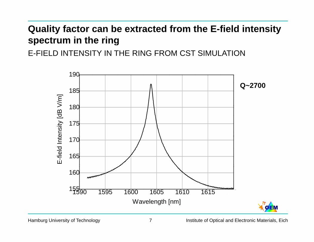
Quality factor can be extracted from the E-field intensity spectrum in the ringp gE-FIELD INTENSITY IN THE RING FROM CST SIMULATION
190
180
185
190
V/m
]
Q~2700
175
180
ensi
ty [d
B V
165
170
E-fi
eld
Inte
1590 1595 1600 1605 1610 1615 1620155
160
Hamburg University of Technology Institute of Optical and Electronic Materials, Eich7
Wavelength [nm]
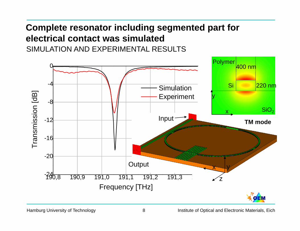
Complete resonator including segmented part for electrical contact was simulated
0
SIMULATION AND EXPERIMENTAL RESULTS
400 nmPolymer
8
-4 Simulation ExperimentdB
] 220 nm
y
Si
-12
-8
smis
sion
[
InputSiO2x
TM mode
-20
-16
Tran
s
190,8 190,9 191,0 191,1 191,2 191,3 19-24
Frequency [THz]
Output x y
z
Hamburg University of Technology Institute of Optical and Electronic Materials, Eich8
Frequency [THz]
1. Overview1. Overview
2. Ring Resonators
3. 3D Photonic Crystals
4. 2D Photonic Crystals
5. Summary5 Su a y
Hamburg University of Technology Institute of Optical and Electronic Materials, Eich9
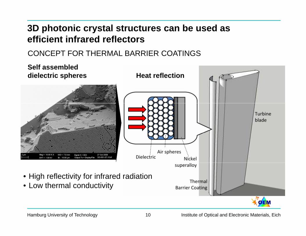
3D photonic crystal structures can be used as efficient infrared reflectorsCONCEPT FOR THERMAL BARRIER COATINGS
Self assembled di l t i h H t fl tidielectric spheres Heat reflection
• High reflectivity for infrared radiation• Low thermal conductivity
Hamburg University of Technology Institute of Optical and Electronic Materials, Eich10
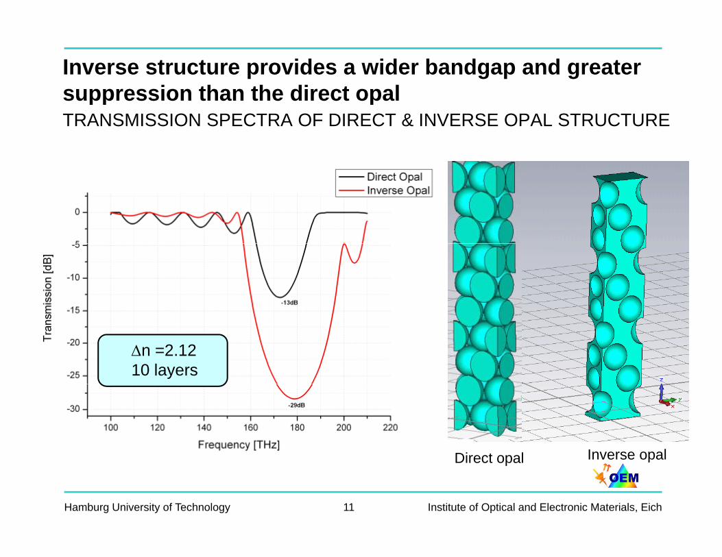
Inverse structure provides a wider bandgap and greater suppression than the direct opalpp pTRANSMISSION SPECTRA OF DIRECT & INVERSE OPAL STRUCTURE
Δn =2.1210 layers
Inverse opalDi t l
Hamburg University of Technology Institute of Optical and Electronic Materials, Eich11
Inverse opalDirect opal
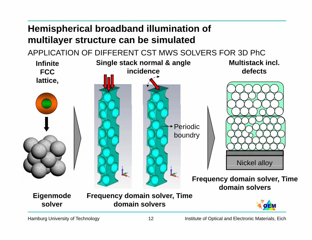
Hemispherical broadband illumination of multilayer structure can be simulatedAPPLICATION OF DIFFERENT CST MWS SOLVERS FOR 3D PhC
y
Infinite FCC
Single stack normal & angle incidence
Multistack incl.defects
lattice,
Periodic boundryboundry
Nickel alloy
Eigenmode Frequency domain solver Time
Frequency domain solver, Time domain solvers
y
Hamburg University of Technology Institute of Optical and Electronic Materials, Eich12
Eigenmode solver
Frequency domain solver, Time domain solvers
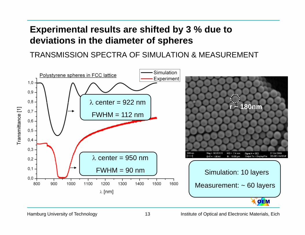
Experimental results are shifted by 3 % due to deviations in the diameter of spheresdeviations in the diameter of spheresTRANSMISSION SPECTRA OF SIMULATION & MEASUREMENT
λ center = 922 nm r ~ 180nmλ center = 922 nm
FWHM = 112 nm
λ center = 950 nm
FWHM = 90 nm Simulation: 10 layers
Measurement: ~ 60 layers
Hamburg University of Technology Institute of Optical and Electronic Materials, Eich13
1. Overview1. Overview
2. Ring Resonators
3. 3D Photonic Crystals
4. 2D Photonic Crystals
5. Summary5 Su a y
Hamburg University of Technology Institute of Optical and Electronic Materials, Eich14
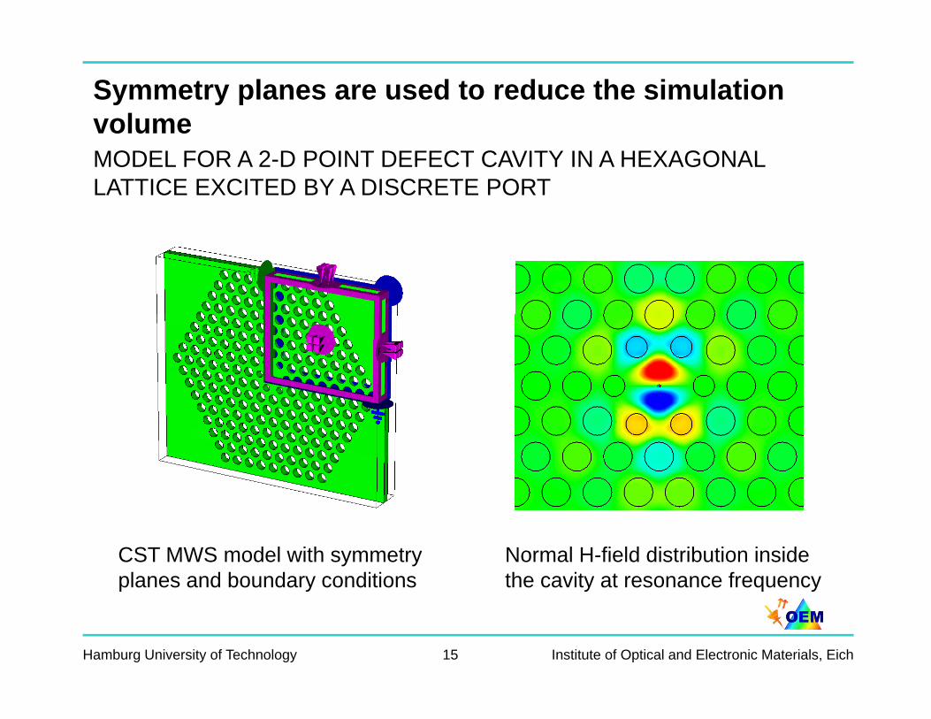
Symmetry planes are used to reduce the simulation volumevolumeMODEL FOR A 2-D POINT DEFECT CAVITY IN A HEXAGONAL LATTICE EXCITED BY A DISCRETE PORT
CST MWS model with symmetry planes and boundary conditions
Normal H-field distribution inside the cavity at resonance frequency
Hamburg University of Technology Institute of Optical and Electronic Materials, Eich15
planes and boundary conditions the cavity at resonance frequency
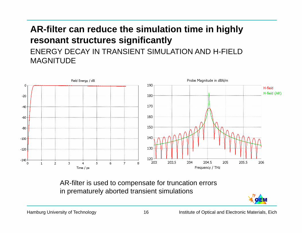
AR-filter can reduce the simulation time in highly resonant structures significantlyresonant structures significantlyENERGY DECAY IN TRANSIENT SIMULATION AND H-FIELD MAGNITUDE
AR-filter is used to compensate for truncation errors in prematurely aborted transient simulations
Hamburg University of Technology Institute of Optical and Electronic Materials, Eich16
in prematurely aborted transient simulations
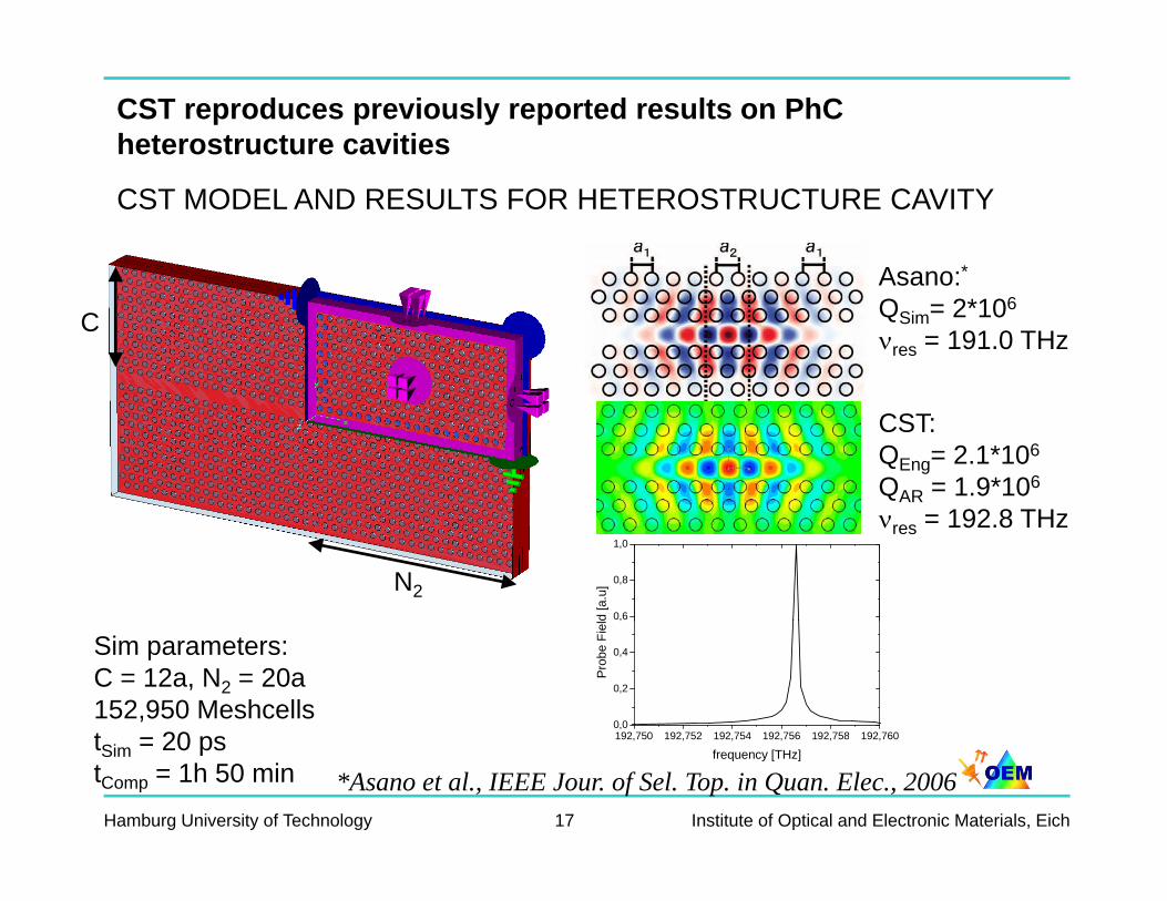
CST reproduces previously reported results on PhC heterostructure cavities
CST MODEL AND RESULTS FOR HETEROSTRUCTURE CAVITY
Asano:*Asano:QSim= 2*106
νres = 191.0 THzC
CST:QEng= 2.1*106
QAR = 1.9*106
νres = 192.8 THz
N20,6
0,8
1,0
d [a
.u]
Sim parameters:C = 12a, N2 = 20a152,950 Meshcellst 20 192 750 192 752 192 754 192 756 192 758 192 760
0,0
0,2
0,4
Pro
be F
iel
Hamburg University of Technology Institute of Optical and Electronic Materials, Eich17
*Asano et al., IEEE Jour. of Sel. Top. in Quan. Elec., 2006tSim = 20 pstComp = 1h 50 min
192,750 192,752 192,754 192,756 192,758 192,760
frequency [THz]
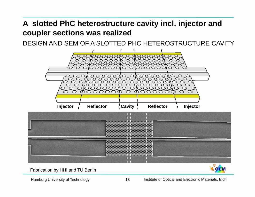
A slotted PhC heterostructure cavity incl. injector and coupler sections was realizedpDESIGN AND SEM OF A SLOTTED PHC HETEROSTRUCTURE CAVITY
Cavity ReflectorReflectorInjector Injector
Hamburg University of Technology Institute of Optical and Electronic Materials, Eich18
Fabrication by HHI and TU Berlin
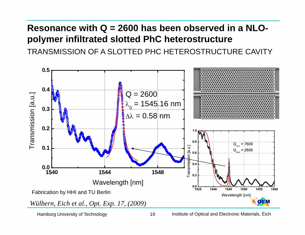
Resonance with Q = 2600 has been observed in a NLO-polymer infiltrated slotted PhC heterostructure p yTRANSMISSION OF A SLOTTED PHC HETEROSTRUCTURE CAVITY
0.5
0.4
a.u.
] Q = 2600λ = 1545 16 nm
0.2
0.3
smis
sion
[a λ0 = 1545.16 nmΔλ = 0.58 nm
0.1Tran
s
1540 1544 15480.0
Wavelength [nm]Fabrication by HHI and TU Berlin
Hamburg University of Technology Institute of Optical and Electronic Materials, Eich19
Fabrication by HHI and TU Berlin
Wülbern, Eich et al., Opt. Exp. 17, (2009)
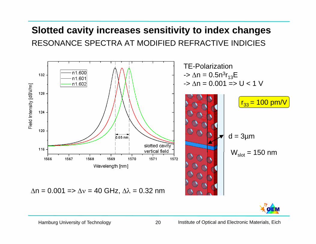
Slotted cavity increases sensitivity to index changesRESONANCE SPECTRA AT MODIFIED REFRACTIVE INDICIESRESONANCE SPECTRA AT MODIFIED REFRACTIVE INDICIES
TE-Polarization-> Δn = 0 5n3r13E> Δn 0.5n r13E-> Δn = 0.001 => U < 1 V
r33 = 100 pm/V
d = 3µmd 3µm
Wslot = 150 nm
Δn = 0.001 => Δν = 40 GHz, Δλ = 0.32 nm
Hamburg University of Technology Institute of Optical and Electronic Materials, Eich20
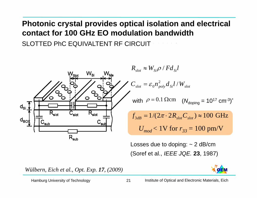
Photonic crystal provides optical isolation and electrical contact for 100 GHz EO modulation bandwidthSLOTTED PhC EQUIVALTENT RF CIRCUIT cm1.0 Ω=ρ
lFdWR SiSislot /ρ≈
slotSipolyslot WldnC /20ε= slotSipolyslot 0
with (Ndoping = 1017 cm-3)*cm1.0 Ω=ρ
GHz100)22/(13 ≈⋅= slotslotdB CRf π
Umod < 1V for r33 = 100 pm/V
Losses due to doping: ~ 2 dB/cm(Soref et al., IEEE JQE. 23, 1987)
Hamburg University of Technology Institute of Optical and Electronic Materials, Eich21
Wülbern, Eich et al., Opt. Exp. 17, (2009)
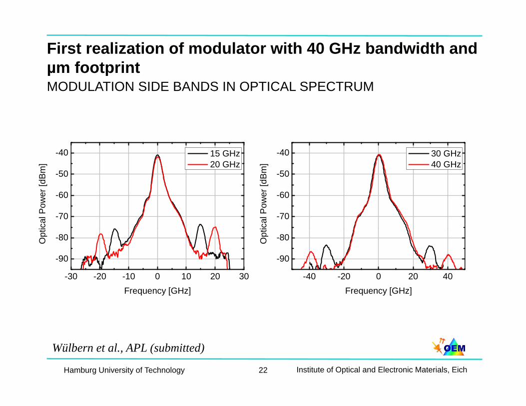
First realization of modulator with 40 GHz bandwidth and µm footprint µ pMODULATION SIDE BANDS IN OPTICAL SPECTRUM
-50
-40
Bm]
30 GHz 40 GHz
-50
-40
Bm]
15 GHz 20 GHz
-70
-60
ical
Pow
er [d
B
-70
-60
ical
Pow
er [d
B
-40 -20 0 20 40
-90
-80Opt
i-30 -20 -10 0 10 20 30
-90
-80Opt
i
Frequency [GHz]Frequency [GHz]
Hamburg University of Technology Institute of Optical and Electronic Materials, Eich22
Wülbern et al., APL (submitted)
1. Overview1. Overview
2. Ring Resonators
3. 3D Photonic Crystals
4. 2D Photonic Crystals
5. Summary5 Su a y
Hamburg University of Technology Institute of Optical and Electronic Materials, Eich23
Summary
• Simulation of strip and slot waveguides with CST MWS has• Simulation of strip and slot waveguides with CST MWS has been shown
• Q-factor extraction from time domain simulations isQ factor extraction from time domain simulations is demonstrated for ring resonators and 2D photonic crystals
• Frequency solver is used to determine angle dependent q y g ptransmission spectra of 3D photonic crystals
• A photonic crystal cavity for GHz amplitude modulation is discussed
Hamburg University of Technology Institute of Optical and Electronic Materials, Eich24
Related Documents