Characterization of PECVD Silicon Nitride Photonic Components at 532 and 900 nm Wavelength P. Neutens a,b , A. Subramanian c , M. Ul Hasan a , C. Chen a , R. Jansen a , T. Claes a , X. Rottenberg a , B. Du Bois a , K. Leyssens a , P. Helin a , S. Severi a , A. Dhakal c , F. Peyskens c , L. Lagae a,b , P. Deshpande a , R. Baets c and P. Van Dorpe a,b a IMEC, Kapeldreef 75, Leuven 3001, Belgium; b Department of Physics, Solid State Physics and Magnetism, KU Leuven, Leuven, Belgium; c Photonics Research Group, Centre for Nano- and Biophotonics, Ghent University-IMEC, Ghent 9000, Belgium ABSTRACT Low temperature PECVD silicon nitride photonic waveguides have been fabricated by both electron beam lithography and 200 mm DUV lithography. Propagation losses and bend losses were both measured at 532 and 900 nm wavelength, revealing sub 1dB/cm propagation losses for cladded waveguides at both wavelengths for single mode operation. Without cladding, propagation losses were measured to be in the 1-3 dB range for 532 nm and remain below 1 dB/cm for 900 nm for single mode waveguides. Bend losses were measured for 532 nm and were well below 0.1 dB per 90 degree bend for radii larger than 10 μm. Keywords: Silicon nitride, Photonic waveguides, PECVD, Ring resonators, propagation losses, bend losses. 1. INTRODUCTION On-chip photonic elements have the potential to serve as platform for data transmission applications. Also for biophotonic sensing applications, waveguides and integrated resonators have been proposed as sensing platforms. However most effort has been put in the development of silicon based photonic components for telecom wavelengths. Although silicon waveguide based optical elements have already been used for biosensing 1 , applications based on Raman spectroscopy 2 or fluorescence 3 often require the use of visible or near infrared wavelengths. Silicon nitride offers a very attractive photonic platform for the development of high-performance low-loss photonic component for wavelengths in the visible and near infrared wavelength regime, where silicon behaves a semiconductor and as a consequence suffers from large free carrier absorption. Also two photon absorption is strongly reduced for longer wavelengths. In previous publications, waveguides and resonators were fabricated in low-pressure chemical vapor deposition (LPCVD) silicon nitride (SiN), mainly due to the very low material losses in the wavelength range of interest and very good uniformity across the wafer while maintaining a reasonably high refractive index 4,5 . However LPCVD is a high temperature process, limiting the fabrication options of semiconductor and metal processing. At Imec, a low temperature PECVD process was developed in order to obtain PECVD silicon nitride layers with good homogeneity across the wafer, a low material loss and low autofluorescence. In this work we will demonstrate that waveguides in PECVD silicon nitride can be fabricated with low propagation loss for visible and NIR wavelengths. The bend loss will be studied for waveguides with and without CVD oxide cladding. Also ring resonators will be modeled, fabricated and measured. Details of the design and simulations of the waveguides and resonators can be found in the second section. In the third section the fabrication will be discussed in detail. The experimental demonstration of the waveguides and ring and disk resonators will be handled, and the different loss mechanisms, directional coupling and Q-factors will be discussed. The conclusions are made in section five. Silicon Photonics and Photonic Integrated Circuits IV, edited by Laurent Vivien, Seppo Honkanen, Lorenzo Pavesi, Stefano Pelli, Proc. of SPIE Vol. 9133, 91331F · © 2014 SPIE CCC code: 0277-786X/14/$18 · doi: 10.1117/12.2052119 Proc. of SPIE Vol. 9133 91331F-1 Downloaded From: http://spiedigitallibrary.org/ on 12/23/2014 Terms of Use: http://spiedl.org/terms

Welcome message from author
This document is posted to help you gain knowledge. Please leave a comment to let me know what you think about it! Share it to your friends and learn new things together.
Transcript

Characterization of PECVD Silicon Nitride Photonic Components at
532 and 900 nm Wavelength
P. Neutensa,b, A. Subramanianc, M. Ul Hasana, C. Chena, R. Jansena, T. Claesa, X. Rottenberga, B.
Du Boisa, K. Leyssensa, P. Helina, S. Severia, A. Dhakalc, F. Peyskensc, L. Lagaea,b, P. Deshpandea,
R. Baetsc and P. Van Dorpea,b
aIMEC, Kapeldreef 75, Leuven 3001, Belgium; bDepartment of Physics, Solid State Physics and
Magnetism, KU Leuven, Leuven, Belgium; cPhotonics Research Group, Centre for Nano- and
Biophotonics, Ghent University-IMEC, Ghent 9000, Belgium
ABSTRACT
Low temperature PECVD silicon nitride photonic waveguides have been fabricated by both electron beam lithography
and 200 mm DUV lithography. Propagation losses and bend losses were both measured at 532 and 900 nm wavelength,
revealing sub 1dB/cm propagation losses for cladded waveguides at both wavelengths for single mode operation.
Without cladding, propagation losses were measured to be in the 1-3 dB range for 532 nm and remain below 1 dB/cm
for 900 nm for single mode waveguides. Bend losses were measured for 532 nm and were well below 0.1 dB per 90
degree bend for radii larger than 10 μm.
Keywords: Silicon nitride, Photonic waveguides, PECVD, Ring resonators, propagation losses, bend losses.
1. INTRODUCTION
On-chip photonic elements have the potential to serve as platform for data transmission applications. Also for
biophotonic sensing applications, waveguides and integrated resonators have been proposed as sensing platforms.
However most effort has been put in the development of silicon based photonic components for telecom wavelengths.
Although silicon waveguide based optical elements have already been used for biosensing1, applications based on Raman spectroscopy2 or fluorescence3 often require the use of visible or near infrared wavelengths. Silicon nitride offers
a very attractive photonic platform for the development of high-performance low-loss photonic component for
wavelengths in the visible and near infrared wavelength regime, where silicon behaves a semiconductor and as a
consequence suffers from large free carrier absorption. Also two photon absorption is strongly reduced for longer
wavelengths. In previous publications, waveguides and resonators were fabricated in low-pressure chemical vapor
deposition (LPCVD) silicon nitride (SiN), mainly due to the very low material losses in the wavelength range of interest
and very good uniformity across the wafer while maintaining a reasonably high refractive index4,5. However LPCVD is a
high temperature process, limiting the fabrication options of semiconductor and metal processing. At Imec, a low
temperature PECVD process was developed in order to obtain PECVD silicon nitride layers with good homogeneity
across the wafer, a low material loss and low autofluorescence.
In this work we will demonstrate that waveguides in PECVD silicon nitride can be fabricated with low propagation loss for visible and NIR wavelengths. The bend loss will be studied for waveguides with and without CVD oxide
cladding. Also ring resonators will be modeled, fabricated and measured. Details of the design and simulations of the
waveguides and resonators can be found in the second section. In the third section the fabrication will be discussed in
detail. The experimental demonstration of the waveguides and ring and disk resonators will be handled, and the different
loss mechanisms, directional coupling and Q-factors will be discussed. The conclusions are made in section five.
Silicon Photonics and Photonic Integrated Circuits IV, edited by Laurent Vivien, Seppo Honkanen,Lorenzo Pavesi, Stefano Pelli, Proc. of SPIE Vol. 9133, 91331F · © 2014 SPIE
CCC code: 0277-786X/14/$18 · doi: 10.1117/12.2052119
Proc. of SPIE Vol. 9133 91331F-1
Downloaded From: http://spiedigitallibrary.org/ on 12/23/2014 Terms of Use: http://spiedl.org/terms

1 8- nioxide
1 80 - TEO, oxide claddingTE1, oxide claddingTMO, oxide cladding
1.7 5 - - TEO, air cladding- - - TE1, air cladding
1.70 -TMO, air cladding
1.65 -
1.60 -
1.55
1.50 -
1.45300
......... ..... ........... . r. .._
400 500 600 700 800 900 1000
Width (nm)
1.70
1.65
1.60
1.55
1.50
1.45500 600 700 800 900 1000 1100 1200 1300
Width (nm)
- n oxide- TEO, oxide cladding- - - - TE1, oxide cladding
TMO, oxide cladding- TEO,aircladding- - - TE1, air cladding
TMO, air cladding
2. DESIGN AND SIMULATION
In order to ensure single mode operation for both wavelengths, we calculated the dispersion curves for the first two TE
modes and the fundamental TM mode for 2 µm PECVD oxide top cladding and air cladding (Fig. 1a and 1b). The
Fimmwave mode solver was used for the design of the waveguide. Refractive indices of the oxide and nitride were taken
from in-line ellipsometry data. Waveguides for 532 nm wavelength operation have a 180 nm thickness, while 220 nm
thickness was chosen for 900 nm wavelength. We calculated that in order to avoid leakage into the substrate, a minimum
bottom cladding thickness of 1.5 µm is necessary. Therefore, we chose a bottom oxide cladding of 2 µm for 532 nm
wavelength and 2.4 µm for 900 nm, in order to optimize the grating coupler efficiency. For TE polarization, the cladded
waveguides for 532 nm display single mode behavior for widths below 380 nm, while uncladded waveguides are single
mode until 530 nm. At 900 nm, the oxide and air cladded waveguides show single mode operation for widths below
respectively 770 and 1100 nm.
Figure 1: Dispersion diagram for (a) 532 nm wavelength and (b) 900 nm wavelength. TE0, TE1 and TM0
modes are plotted for oxide and air cladding.
3. FABRICATION
To build Silicon nitride photonic components, we deposit 2 μm high-density plasma CVD oxide on a 200 mm bare silicon wafer. On top, the waveguide material, 180 or 220 nm PECVD Silicon nitride is deposited. In previous
publications LPCVD nitride was favored due to its better homogeneity of material index and thickness. At Imec6, a
nitride PECVD process at low temperature was optimized to achieve low propagation loss, low auto-fluorescence and
good control over the thickness and index of the nitride. The PECVD SiN deposition process is based on SiH4, N2 and
NH3 and is performed at 400 °C, which ensures CMOS back-end compatibility. The refractive index of the SiN was
measured to be 1.91 for a wavelength of 532 nm and 1.88 for 900 nm. A standard 9-point thickness measurement was
performed on a test wafer from the same lot. An average thickness of 178.9 nm was obtained with a standard deviation
of 4.6 nm for a targeted value of 180 nm. The minimum and maximum thicknesses were 174.2 and 186.2 nm
respectively. AFM scans were performed in order to assess the top surface roughness of both the SiO2 and SiN films.
Over an area of 2 μm x 2 μm, the RMS roughness value for the 2 μm HDP SiO2 film was measured to be extremely low
at 0.13 nm and a 100 nm SiN film deposited on top of the oxide exhibited a very low RMS roughness value of 0.28 nm.
(b) (a)
Proc. of SPIE Vol. 9133 91331F-2
Downloaded From: http://spiedigitallibrary.org/ on 12/23/2014 Terms of Use: http://spiedl.org/terms
cc.VS
pot Magn
Det W
D E
xp20 pm
.00 kV 3.0
1817xT
LD 5.5
1h .://w
ww
.imec.be
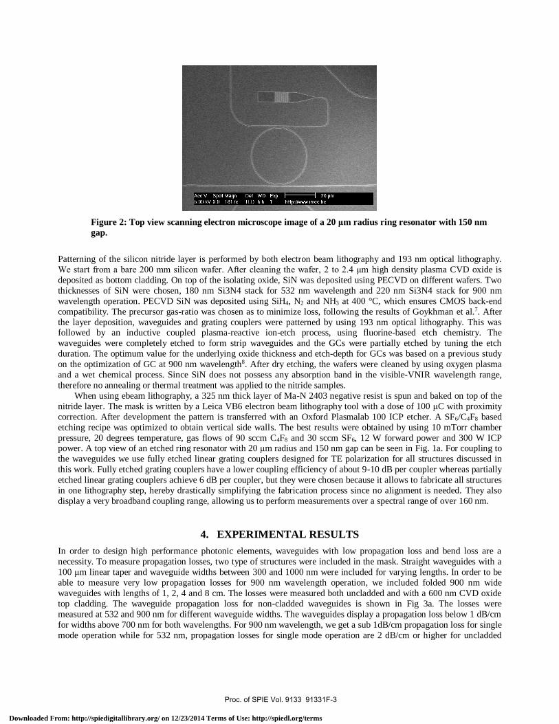
Figure 2: Top view scanning electron microscope image of a 20 μm radius ring resonator with 150 nm
gap.
Patterning of the silicon nitride layer is performed by both electron beam lithography and 193 nm optical lithography.
We start from a bare 200 mm silicon wafer. After cleaning the wafer, 2 to 2.4 μm high density plasma CVD oxide is
deposited as bottom cladding. On top of the isolating oxide, SiN was deposited using PECVD on different wafers. Two
thicknesses of SiN were chosen, 180 nm Si3N4 stack for 532 nm wavelength and 220 nm Si3N4 stack for 900 nm
wavelength operation. PECVD SiN was deposited using SiH4, N2 and NH3 at 400 °C, which ensures CMOS back-end
compatibility. The precursor gas-ratio was chosen as to minimize loss, following the results of Goykhman et al.7. After
the layer deposition, waveguides and grating couplers were patterned by using 193 nm optical lithography. This was followed by an inductive coupled plasma-reactive ion-etch process, using fluorine-based etch chemistry. The
waveguides were completely etched to form strip waveguides and the GCs were partially etched by tuning the etch
duration. The optimum value for the underlying oxide thickness and etch-depth for GCs was based on a previous study
on the optimization of GC at 900 nm wavelength8. After dry etching, the wafers were cleaned by using oxygen plasma
and a wet chemical process. Since SiN does not possess any absorption band in the visible-VNIR wavelength range,
therefore no annealing or thermal treatment was applied to the nitride samples.
When using ebeam lithography, a 325 nm thick layer of Ma-N 2403 negative resist is spun and baked on top of the
nitride layer. The mask is written by a Leica VB6 electron beam lithography tool with a dose of 100 μC with proximity
correction. After development the pattern is transferred with an Oxford Plasmalab 100 ICP etcher. A SF6/C4F8 based
etching recipe was optimized to obtain vertical side walls. The best results were obtained by using 10 mTorr chamber
pressure, 20 degrees temperature, gas flows of 90 sccm C4F8 and 30 sccm SF6, 12 W forward power and 300 W ICP power. A top view of an etched ring resonator with 20 μm radius and 150 nm gap can be seen in Fig. 1a. For coupling to
the waveguides we use fully etched linear grating couplers designed for TE polarization for all structures discussed in
this work. Fully etched grating couplers have a lower coupling efficiency of about 9-10 dB per coupler whereas partially
etched linear grating couplers achieve 6 dB per coupler, but they were chosen because it allows to fabricate all structures
in one lithography step, hereby drastically simplifying the fabrication process since no alignment is needed. They also
display a very broadband coupling range, allowing us to perform measurements over a spectral range of over 160 nm.
4. EXPERIMENTAL RESULTS
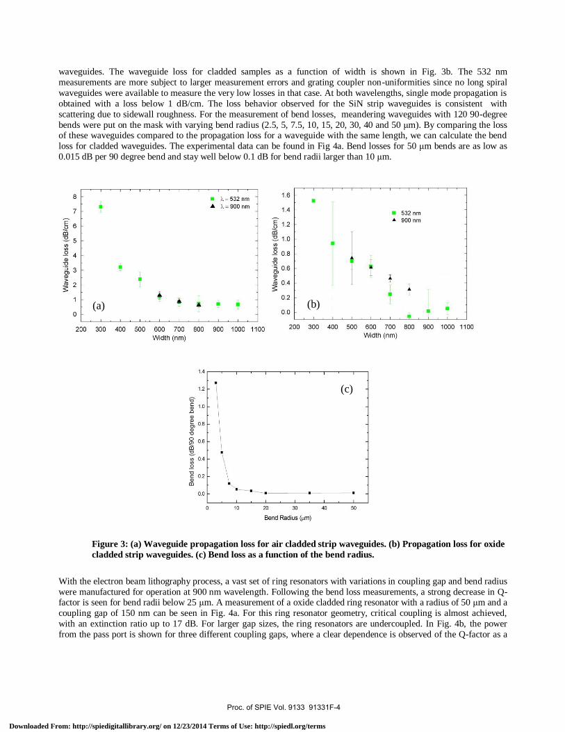
In order to design high performance photonic elements, waveguides with low propagation loss and bend loss are a
necessity. To measure propagation losses, two type of structures were included in the mask. Straight waveguides with a
100 μm linear taper and waveguide widths between 300 and 1000 nm were included for varying lengths. In order to be
able to measure very low propagation losses for 900 nm wavelength operation, we included folded 900 nm wide
waveguides with lengths of 1, 2, 4 and 8 cm. The losses were measured both uncladded and with a 600 nm CVD oxide
top cladding. The waveguide propagation loss for non-cladded waveguides is shown in Fig 3a. The losses were
measured at 532 and 900 nm for different waveguide widths. The waveguides display a propagation loss below 1 dB/cm
for widths above 700 nm for both wavelengths. For 900 nm wavelength, we get a sub 1dB/cm propagation loss for single
mode operation while for 532 nm, propagation losses for single mode operation are 2 dB/cm or higher for uncladded
Proc. of SPIE Vol. 9133 91331F-3
Downloaded From: http://spiedigitallibrary.org/ on 12/23/2014 Terms of Use: http://spiedl.org/terms
8
7
' 3
32
1
o
X=532nm -X=900 nm
200 300 400 500 600 700Width (nm)
800 900 1000 1100
1.6
1.4
ti
2 0.8v'5 0.6ti
0.4
0.2
0.0
i
532 nm909 nm
200 300 400 500 600 700Width (nm)
800 900 1000 1100
O g O
Ben
d lo
ss (
dB /9
0 de
gree
ben
d)0
00
00
ON
AO
OD
ON
waveguides. The waveguide loss for cladded samples as a function of width is shown in Fig. 3b. The 532 nm
measurements are more subject to larger measurement errors and grating coupler non-uniformities since no long spiral
waveguides were available to measure the very low losses in that case. At both wavelengths, single mode propagation is
obtained with a loss below 1 dB/cm. The loss behavior observed for the SiN strip waveguides is consistent with
scattering due to sidewall roughness. For the measurement of bend losses, meandering waveguides with 120 90-degree
bends were put on the mask with varying bend radius (2.5, 5, 7.5, 10, 15, 20, 30, 40 and 50 μm). By comparing the loss of these waveguides compared to the propagation loss for a waveguide with the same length, we can calculate the bend
loss for cladded waveguides. The experimental data can be found in Fig 4a. Bend losses for 50 μm bends are as low as
0.015 dB per 90 degree bend and stay well below 0.1 dB for bend radii larger than 10 μm.
Figure 3: (a) Waveguide propagation loss for air cladded strip waveguides. (b) Propagation loss for oxide
cladded strip waveguides. (c) Bend loss as a function of the bend radius.
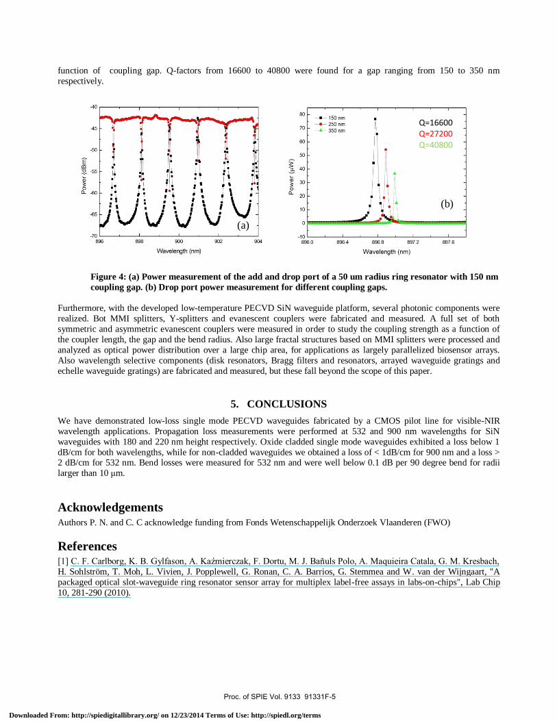
With the electron beam lithography process, a vast set of ring resonators with variations in coupling gap and bend radius
were manufactured for operation at 900 nm wavelength. Following the bend loss measurements, a strong decrease in Q-factor is seen for bend radii below 25 μm. A measurement of a oxide cladded ring resonator with a radius of 50 μm and a
coupling gap of 150 nm can be seen in Fig. 4a. For this ring resonator geometry, critical coupling is almost achieved,
with an extinction ratio up to 17 dB. For larger gap sizes, the ring resonators are undercoupled. In Fig. 4b, the power
from the pass port is shown for three different coupling gaps, where a clear dependence is observed of the Q-factor as a
(a) (b)
(c)
Proc. of SPIE Vol. 9133 91331F-4
Downloaded From: http://spiedigitallibrary.org/ on 12/23/2014 Terms of Use: http://spiedl.org/terms
4s
-rno-o_o_
function of coupling gap. Q-factors from 16600 to 40800 were found for a gap ranging from 150 to 350 nm
respectively.
Figure 4: (a) Power measurement of the add and drop port of a 50 um radius ring resonator with 150 nm
coupling gap. (b) Drop port power measurement for different coupling gaps.
Furthermore, with the developed low-temperature PECVD SiN waveguide platform, several photonic components were
realized. Bot MMI splitters, Y-splitters and evanescent couplers were fabricated and measured. A full set of both
symmetric and asymmetric evanescent couplers were measured in order to study the coupling strength as a function of
the coupler length, the gap and the bend radius. Also large fractal structures based on MMI splitters were processed and
analyzed as optical power distribution over a large chip area, for applications as largely parallelized biosensor arrays.
Also wavelength selective components (disk resonators, Bragg filters and resonators, arrayed waveguide gratings and
echelle waveguide gratings) are fabricated and measured, but these fall beyond the scope of this paper.
5. CONCLUSIONS
We have demonstrated low-loss single mode PECVD waveguides fabricated by a CMOS pilot line for visible-NIR
wavelength applications. Propagation loss measurements were performed at 532 and 900 nm wavelengths for SiN
waveguides with 180 and 220 nm height respectively. Oxide cladded single mode waveguides exhibited a loss below 1
dB/cm for both wavelengths, while for non-cladded waveguides we obtained a loss of < 1dB/cm for 900 nm and a loss > 2 dB/cm for 532 nm. Bend losses were measured for 532 nm and were well below 0.1 dB per 90 degree bend for radii
larger than 10 μm.
Acknowledgements Authors P. N. and C. C acknowledge funding from Fonds Wetenschappelijk Onderzoek Vlaanderen (FWO)
References [1] C. F. Carlborg, K. B. Gylfason, A. Kaźmierczak, F. Dortu, M. J. Bañuls Polo, A. Maquieira Catala, G. M. Kresbach,
H. Sohlström, T. Moh, L. Vivien, J. Popplewell, G. Ronan, C. A. Barrios, G. Stemmea and W. van der Wijngaart, "A
packaged optical slot-waveguide ring resonator sensor array for multiplex label-free assays in labs-on-chips", Lab Chip
10, 281-290 (2010).
Q=16600
Q=27200
Q=40800
(b)
(a)
Proc. of SPIE Vol. 9133 91331F-5
Downloaded From: http://spiedigitallibrary.org/ on 12/23/2014 Terms of Use: http://spiedl.org/terms
[2] P. C. Ashok, G. P. Singh, H. A. Rendall, T. F. Kraussa and K. Dholakia, "Waveguide confined Raman spectroscopy
for microfluidic interrogation", Lab Chip 11 (7), 1262–1272 (2011).
[3] S. Kühn, P. Measor, E. J. Lunt, B. S. Phillips, D. W. Deamer, A. R. Hawkins and H. Schmidt , "Loss-based optical
trap for on-chip particle analysis", Lab Chip 9 (15), 2212–2216 (2009).
[4] M Melchiorri, N. Daldosso, F. Sbrana, L. Pavesi, G. Pucker, C. Kompocholis, P. Bellutti and A. Lui , "Propagation
losses of silicon nitride waveguides in the near-infrared range", Appl. Phys. Lett. 86, 121111 (2005).
[5] E. S. Hosseini, S. Yegnanarayanan, A. Hossein Atabaki, M. Soltani, and A. Adibi, "High Quality Planar Silicon
Nitride Microdisk Resonators for Integrated Photonics in the Visible Wavelength Range", Opt. Express 17, 14543-14551
(2009).
[6] A. Z. Subramanian, P. Neutens, A. Dhakal, R. Jansen, T. Claes, X. Rottenberg, F. Peyskens, S. Selvaraja, P. Helin,
B. Du Bois, K. Leyssens, S. Severi, P. Deshpande, R. Baets and P. Van Dorpe, "Low-loss singlemode PECVD silicon
nitride photonic wire waveguides for 532-900 nm wavelength window fabricated within a CMOS pilot line", IEEE
Photonics Journal 5 (6), 2202809 (2013).
[7] I. Goykhman, B. Desiatov and U. Levy, "Ultrathin silicon nitride microring resonator for bio-photonic applications at
970 nm wavelength", Appl. Phys. Lett. 97 (8), 081108-1–081108-3 (2010).
[8] A. Z. Subramanian, S. Selvaraja, P. Verheyen, A. Dhakal, K. Komorowska, and R. Baets, "Near-infrared grating
couplers for silicon nitride photonic wires", Photon. Technol. 24 (19), 1700–1703 (2012).
Proc. of SPIE Vol. 9133 91331F-6
Downloaded From: http://spiedigitallibrary.org/ on 12/23/2014 Terms of Use: http://spiedl.org/terms
Related Documents