Characterization of laser ablated silicon thin films S. Vijayalakshmi a , Z. Iqbal b , M.A. George c , J. Federici d , H. Grebel a, * a Optical Waveguide Laboratory, Electrical and Computer Engineering,New Jersey Institute of Technology, Newark, NJ 07102, USA b Research and Technology, Allied Signal Inc., Morristown, NJ 07962, USA c University Of Alabama at Huntsville, Huntsville, AL 35899, USA d Department of Physics, New Jersey Institute Of Technology, Newark, NJ 07102, USA Received 11 November 1997; accepted 24 July 1998 Abstract Using laser ablation, we deposited silicon layers consisting of clusters and crystalline domains onto glass, quartz, aluminum, titanium, copper, single-crystal silicon and single-crystal potassium bromide substrates. The microstructure and the morphology of the films were characterized by use of optical microscopy, laser scanning microscopy, atomic force microscopy, transmission electron microscopy, micro- Raman spectroscopy, X-ray photoelectron spectroscopy and X-ray diffraction. The results indicated that the deposited material was composed of microcrystalline droplets, typically 3.5 mm in diameter, separated by amorphous-like regions. The droplets were composed of crystalline material at their centers and an outer halo of nanometer-size particles. q 1999 Elsevier Science S.A. All rights reserved. Keywords: Nanostructures; Raman scattering; Transmission electron microscopy (TEM); X-ray diffraction 1. Introduction The unique non-linear properties of laser ablated silicon samples measured recently in our laboratory [1,2], led us to characterize them extensively by use of various techniques: optical microscopy (OM), laser scanning microscopy (LSM), atomic force microscopy (AFM), transmission elec- tron microscopy (TEM), micro-Raman spectroscopy, X-ray photoelectron spectroscopy (XPS) and X-ray diffraction (XRD). It is well known that nanometer size clusters show an increase in the non-linear optical coefficients compared to bulk materials. This increase may be as large as two orders of magnitude [3,4] and was largely attributed to confinement of electron and hole states within small dimen- sions. As the clusters become of the order of 20 nm, exci- tonic states possess energy values comparable to the inter- band separation and, therefore, may take part in the non- linear process. In contrast, we have measured an increase of more than four orders of magnitude in the real part of the non-linear susceptibility [1,2]. For example, the real part of the non-linear susceptibility, Re{x (3) }, was found to be, 2.28 £ 10 25 esu with non-linear lifetime, t , of 140 ns at l 355 nm. We measured, Re{x 3 } 21:33 £ 10 23 esu and t 5 ns at l 532 nm. These values should be compared with typical values of Re{x 3 } , 10 28 esu for nanoclusters prepared by other methods [3,4]. Thus, it is important to know the morphology and size range of the nanoclusters involved in the non-linear processes. In parti- cular, one would like to find out whether the large non-linear values stem from the existence of closed-packed nanocrys- tallites. If this is the case, useful non-linear, nano-optical materials may be realized. Our films were composed of micrometer size droplets that were made of nanocrystalli- ties. Non-linear optical as well as some of the characteriza- tion techniques (namely, XRD and XPS) were averaged over relatively large sample area. As a result, the droplets may have contributed more to the signal in XRD and XPS. Thus with some caution, we may conclude that the large non-linearities observed are related to these crystallites. The paper is organized as follows. An introduction is provided in Section 1 and the growth of the samples is described in Section 2. In Section 3 we describe our results from the various techniques. These are discussed in Section 4 and conclusions are provided in Section 5. 2. Experiment The silicon films were grown on various substrates by laser ablation. A KrF excimer laser beam (l 248 nm, average power kI l 3 W, pulse duration 8 ns, repetition Thin Solid Films 339 (1999) 102–108 0040-6090/99/$ - see front matter q 1999 Elsevier Science S.A. All rights reserved. PII: S0040-6090(98)01158-4 * Corresponding author.

Welcome message from author
This document is posted to help you gain knowledge. Please leave a comment to let me know what you think about it! Share it to your friends and learn new things together.
Transcript

Characterization of laser ablated silicon thin ®lms
S. Vijayalakshmia, Z. Iqbalb, M.A. Georgec, J. Federicid, H. Grebela,*
aOptical Waveguide Laboratory, Electrical and Computer Engineering,New Jersey Institute of Technology, Newark, NJ 07102, USAbResearch and Technology, Allied Signal Inc., Morristown, NJ 07962, USA
cUniversity Of Alabama at Huntsville, Huntsville, AL 35899, USAdDepartment of Physics, New Jersey Institute Of Technology, Newark, NJ 07102, USA
Received 11 November 1997; accepted 24 July 1998
Abstract
Using laser ablation, we deposited silicon layers consisting of clusters and crystalline domains onto glass, quartz, aluminum, titanium,
copper, single-crystal silicon and single-crystal potassium bromide substrates. The microstructure and the morphology of the ®lms were
characterized by use of optical microscopy, laser scanning microscopy, atomic force microscopy, transmission electron microscopy, micro-
Raman spectroscopy, X-ray photoelectron spectroscopy and X-ray diffraction. The results indicated that the deposited material was
composed of microcrystalline droplets, typically 3.5 mm in diameter, separated by amorphous-like regions. The droplets were composed
of crystalline material at their centers and an outer halo of nanometer-size particles. q 1999 Elsevier Science S.A. All rights reserved.
Keywords: Nanostructures; Raman scattering; Transmission electron microscopy (TEM); X-ray diffraction
1. Introduction
The unique non-linear properties of laser ablated silicon
samples measured recently in our laboratory [1,2], led us to
characterize them extensively by use of various techniques:
optical microscopy (OM), laser scanning microscopy
(LSM), atomic force microscopy (AFM), transmission elec-
tron microscopy (TEM), micro-Raman spectroscopy, X-ray
photoelectron spectroscopy (XPS) and X-ray diffraction
(XRD). It is well known that nanometer size clusters show
an increase in the non-linear optical coef®cients compared
to bulk materials. This increase may be as large as two
orders of magnitude [3,4] and was largely attributed to
con®nement of electron and hole states within small dimen-
sions. As the clusters become of the order of 20 nm, exci-
tonic states possess energy values comparable to the inter-
band separation and, therefore, may take part in the non-
linear process. In contrast, we have measured an increase of
more than four orders of magnitude in the real part of the
non-linear susceptibility [1,2]. For example, the real part of
the non-linear susceptibility, Re{x (3)}, was found to be,
2.28 £ 1025 esu with non-linear lifetime, t , of 140 ns at
l � 355 nm. We measured, Re{x�3�} � 21:33 £ 1023 esu
and t � 5 ns at l � 532 nm. These values should be
compared with typical values of Re{x�3�} , 1028 esu for
nanoclusters prepared by other methods [3,4]. Thus, it is
important to know the morphology and size range of the
nanoclusters involved in the non-linear processes. In parti-
cular, one would like to ®nd out whether the large non-linear
values stem from the existence of closed-packed nanocrys-
tallites. If this is the case, useful non-linear, nano-optical
materials may be realized. Our ®lms were composed of
micrometer size droplets that were made of nanocrystalli-
ties. Non-linear optical as well as some of the characteriza-
tion techniques (namely, XRD and XPS) were averaged
over relatively large sample area. As a result, the droplets
may have contributed more to the signal in XRD and XPS.
Thus with some caution, we may conclude that the large
non-linearities observed are related to these crystallites. The
paper is organized as follows. An introduction is provided in
Section 1 and the growth of the samples is described in
Section 2. In Section 3 we describe our results from the
various techniques. These are discussed in Section 4 and
conclusions are provided in Section 5.
2. Experiment
The silicon ®lms were grown on various substrates by
laser ablation. A KrF excimer laser beam (l � 248 nm,
average power kIl � 3 W, pulse duration 8 ns, repetition
Thin Solid Films 339 (1999) 102±108
0040-6090/99/$ - see front matter q 1999 Elsevier Science S.A. All rights reserved.
PII: S0040-6090(98)01158-4
* Corresponding author.

rate 50 Hz, deposition time 10 min) was focused to a
100 mm spot-size on a Si wafer target (k100l, n-type, 1016
cm23). The Si target was cleaned by hydro¯uoric acid and
methanol while the substrates were cleaned by acetone and
methanol. The substrates were positioned 3 cm from the Si
target. The ambient pressure in the chamber was maintained
at 8 £ 1026 Torr. The substrates were maintained at room
temperature. The size of each substrate was about 1.5 cm £1.5 cm. The samples possessed concentric ring regions with
varying colors. Most of our ®lms could be classi®ed into
three major regions, I, II and III, with colors in transmission
that were faint yellow, yellow, and brown respectively.
These colors probably originated from differences in
absorption for the various regions. Region III extended
between 0±3 mm with respect to the center of the ring.
The radii of rings of regions II and I were 3±4.5 mm and
4.5±6 mm respectively.
3. Results
3.1. Optical microscopy
The ®lms were ®rst inspected by use of an optical micro-
scope and were found to be composed of micrometer-size
droplets as shown in Fig. 1. Smooth regions consisting of
nanometer-size clusters were scattered in between the
droplets as indicated by atomic force microscopy (AFM)
and micro-Raman spectroscopy. The average size of a
droplet was surprisingly similar in all three regions. The
average droplet diameter was 3:63 ^ 2:17 mm,
3:38 ^ 1:48 mm and 3:34 ^ 1:51 mm in regions I, II and
III respectively. The distributions of the droplets were 22,
54, and 76 droplets within a 50 £ 50 mm square in regions I,
II and III respectively. Similar droplet formation was
observed on glass, quartz, aluminum-coated glass, titanium,
and single-crystal KBr and silicon, when the ®lms were
deposited under the same conditions. In addition, most
droplets were circular in shape.
3.2. Scanning laser microscopy
The thickness in each region is not a well de®ned feature
owing to the discontinuous nature of the samples. Therefore,
we prefer to characterize each region by its equivalent thick-
ness. This was achieved with the help of a laser scanning
microscope (LSM, Carl Zeiss, axioplan microscope). We
performed a two-dimensional scan, as shown in Fig. 2, of
the sample which was positioned at various heights with
respect to a reference point (topographical sectioning). A
histogram of the sample height was generated and an esti-
mate of the average height of each droplet was made. The
reference point in Fig. 2 was taken as the level of a crater
S. Vijayalakshmi et al. / Thin Solid Films 339 (1999) 102±108 103
Fig. 1. Optical microscope pictures of the Si sample on a glass substrate in
(a) region I, (b) region II and (c) region III.
Fig. 2. Topographic lines around a clean crater as measured by use of LSM.
Also shown is a histogram of the height occurrence in the sample.

formed by laser ablation of the sample which was silicon
clusters on a glass substrate. The glass substrate was trans-
parent to the laser beam and was visually inspected to make
sure that most of the silicon material was removed and the
glass remained unharmed. As can be seen from Fig. 2, the
average height of a droplet in region II is about 0.8 mm. The
average height of the droplets in regions I, II, and III was
measured to be, 0:6 ^ 0:2 mm, 0:8 ^ 0:2 mm and
2 ^ 0:5 mm, respectively. These droplets were located on
an amorphous-like background ®lm. The average thick-
nesses of the material in regions I, II and III were estimated
from these measurements as 100 nm, 200 nm and 400 nm
respectively. The sample thicknesses were also measured by
use of a pro®lometer. Like the LSM, the pro®lometer probe
averages the features in the height of the layer. Both tech-
niques yielded similar results for the background as well as
for the clusters. The scan with the LSM was repeated with a
lower resolution. The spot-size of the laser was thus
increased, resulting in a larger height averaging. This
number was used when assessing the optical loss (see
below).
3.3. Optical absorption
Fig. 3 shows the optical absorption from a laser ablated
silicon ®lm on glass. The optical absorption spectrum was
obtained by measuring the transmission and re¯ection for
each region assuming an averaged dielectric slab with a
given effective thickness as well as multiple re¯ections
within the slab. The absorption shows features associated
with an effective band gap, particularly at wavelengths in
the blue spectral range. In assessing the absorption for each
region one needs to identify a characteristic ®lm thickness.
The large droplets contributed more to the ®lm optical loss
since absorption depends exponentially on the ®lm thick-
ness. On the other hand, the number of droplets was small
and most of the transmission occurred through the back-
ground layer. In addition, surface roughness effectively
increased absorption values owing to multiple re¯ections
between and within droplets [5]. A practical solution to
the above was to de®ne an effective thickness of the back-
ground layer obtained by a low resolution LSM scan. These
values were 100 nm, 200 nm and 400 nm for regions I, II
and III respectively. This procedure results in an effective
value of the loss, which includes multiple re¯ections.
3.4. X-ray diffraction
X-ray diffraction was used to determine the average size
of the microcrystals and nanocrystals in the sample. A
Rigaku D/MAX-B system with a Cu Ka source and a thin
®lm attachment was used to obtain the diffraction data
displayed in Fig. 4. The data were taken with the X-ray
beam incident at a grazing angle of 28 to enhance the signal
from the thin ®lms, whereas the data for the reference wafer
was taken at 908 to the wafer surface. The k111l, k220l,k311l and k400l crystallographic planes of cubic Si corre-
sponding to 2u values of 28.458, 47.358, 56.28, and 69.38respectively, were identi®ed in the diffraction patterns. The
k400l re¯ection from the k100l oriented Si target was
observed at 69.38. The diffraction data from the laser ablated
samples showed the crystallites were predominantly
oriented along k111l and k220l planes. When different
regions of the ®lms were studied, the X-ray re¯ections
appeared at the same 2u positions, but peak intensities for
region III were observed to be larger owing to the larger
amount of material in this region. We have grown samples
on k100l double-polished Si substrates under similar condi-
tions. Here too, the microcrystallites in the sample were
predominantly oriented on k111l Si planes in contrast to
the k100l orientation of target or substrate crystals.
An attempt was made in each region to calculate the
crystallite size from the half-widths of the X-ray diffraction
lines. High resolution diffraction patterns were taken around
2u � 288 and the data obtained were ®tted to a Gaussian line
shape superimposed on a linear background. The width of
the diffraction line is proportional to the crystallite size. The
latter can be estimated from high resolution X-ray diffrac-
S. Vijayalakshmi et al. / Thin Solid Films 339 (1999) 102±108104
Fig. 3. (a) Transmission and re¯ection from region II. (b) Optical assess-
ment based on the equivalent ®lm thickness of 0.2 mm.
tion data using the Scherrer relation [6]:
B � 0:9l
tcosu�1�
where B is the linewidth at half maximum, l is the X-ray
wavelength, and t is the diameter of the crystal. The data are
displayed in Fig. 5, and as can be seen, the lines observed
from regions II and III have identical full widths at half-
maximum (FWHM) of 0.1678, corresponding to an average
crystallite size of 43 nm. Region I did not show signi®cant
X-ray diffraction line intensities. This estimate represents
the average size of the crystallites within the droplets in
each region as will be discussed below.
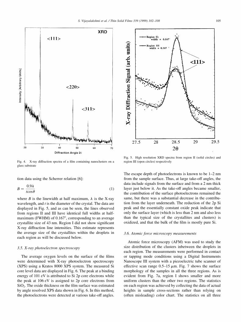
3.5. X-ray photoelectron spectroscopy
The average oxygen levels on the surface of the ®lms
were determined with X-ray photoelectron spectroscopy
(XPS) using a Kratos 8000 XPS system. The measured Si
core level data are displayed in Fig. 6. The peak at a binding
energy of 101 eV is attributed to Si 2p core electrons while
the peak at 106 eV is assigned to 2p core electrons from
SiO2. The oxide thickness on the ®lm surface was estimated
by angle resolved XPS data shown in Fig. 6. In this method,
the photoelectrons were detected at various take-off angles.
The escape depth of photoelectrons is known to be 1±2 nm
from the sample surface. Thus, at large take-off angles, the
data include signals from the surface and from a 2 nm thick
layer just below it. As the take-off angles became smaller,
the contribution of the surface photoelectrons remained the
same, but there was a substantial decrease in the contribu-
tion from the layer underneath. The reduction of the 2p Si
peak and the essentially constant oxide peak indicate that
only the surface layer (which is less than 2 nm and also less
than the typical size of the crystallites and clusters) is
oxidized, and that the bulk of the ®lm is mostly pure Si.
3.6. Atomic force microscopy measurements
Atomic force microscopy (AFM) was used to study the
size distribution of the clusters inbetween the droplets in
each region. The measurements were performed in contact
or tapping mode conditions using a Digital Instruments
Nanoscope III system with a piezoelectric tube scanner of
effective scan range 0.5±15 mm. Fig. 7 shows the surface
morphology of the samples in all the three regions. As is
evident from Fig. 7a, region I shows smaller and more
uniform clusters than the other two regions. The statistics
on each region was achieved by collecting the data of actual
heights in sample cross-sections rather than relying on
(often misleading) color chart. The statistics on all three
S. Vijayalakshmi et al. / Thin Solid Films 339 (1999) 102±108 105
Fig. 4. X-ray diffraction spectra of a ®lm containing nanoclusters on a
glass substrate
Fig. 5. High resolution XRD spectra from region II (solid circles) and
region III (open circles) respectively
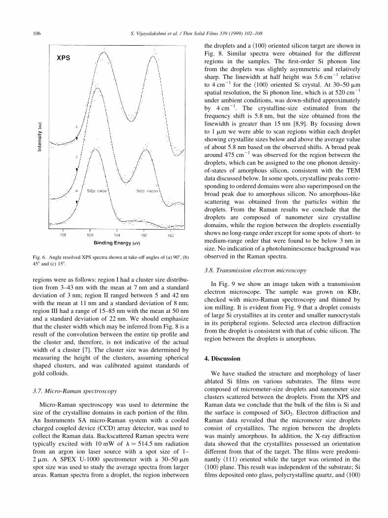
regions were as follows: region I had a cluster size distribu-
tion from 3±43 nm with the mean at 7 nm and a standard
deviation of 3 nm; region II ranged between 5 and 42 nm
with the mean at 11 nm and a standard deviation of 8 nm;
region III had a range of 15±85 nm with the mean at 50 nm
and a standard deviation of 22 nm. We should emphasize
that the cluster width which may be inferred from Fig. 8 is a
result of the convolution between the entire tip pro®le and
the cluster and, therefore, is not indicative of the actual
width of a cluster [7]. The cluster size was determined by
measuring the height of the clusters, assuming spherical
shaped clusters, and was calibrated against standards of
gold colloids.
3.7. Micro-Raman spectroscopy
Micro-Raman spectroscopy was used to determine the
size of the crystalline domains in each portion of the ®lm.
An Instruments SA micro-Raman system with a cooled
charged coupled device (CCD) array detector, was used to
collect the Raman data. Backscattered Raman spectra were
typically excited with 10 mW of l � 514:5 nm radiation
from an argon ion laser source with a spot size of 1±
2 mm. A SPEX U-1000 spectrometer with a 30±50 mm
spot size was used to study the average spectra from larger
areas. Raman spectra from a droplet, the region inbetween
the droplets and a k100l oriented silicon target are shown in
Fig. 8. Similar spectra were obtained for the different
regions in the samples. The ®rst-order Si phonon line
from the droplets was slightly asymmetric and relatively
sharp. The linewidth at half height was 5.6 cm21 relative
to 4 cm21 for the k100l oriented Si crystal. At 30±50 mm
spatial resolution, the Si phonon line, which is at 520 cm21
under ambient conditions, was down-shifted approximately
by 4 cm21. The crystalline-size estimated from the
frequency shift is 5.8 nm, but the size obtained from the
linewidth is greater than 15 nm [8,9]. By focusing down
to 1 mm we were able to scan regions within each droplet
showing crystallite sizes below and above the average value
of about 5.8 nm based on the observed shifts. A broad peak
around 475 cm21 was observed for the region between the
droplets, which can be assigned to the one phonon density-
of-states of amorphous silicon, consistent with the TEM
data discussed below. In some spots, crystalline peaks corre-
sponding to ordered domains were also superimposed on the
broad peak due to amorphous silicon. No amorphous-like
scattering was obtained from the particles within the
droplets. From the Raman results we conclude that the
droplets are composed of nanometer size crystalline
domains, while the region between the droplets essentially
shows no long-range order except for some spots of short- to
medium-range order that were found to be below 3 nm in
size. No indication of a photoluminescence background was
observed in the Raman spectra.
3.8. Transmission electron microscopy
In Fig. 9 we show an image taken with a transmission
electron microscope. The sample was grown on KBr,
checked with micro-Raman spectroscopy and thinned by
ion milling. It is evident from Fig. 9 that a droplet consists
of large Si crystallites at its center and smaller nanocrystals
in its peripheral regions. Selected area electron diffraction
from the droplet is consistent with that of cubic silicon. The
region between the droplets is amorphous.
4. Discussion
We have studied the structure and morphology of laser
ablated Si ®lms on various substrates. The ®lms were
composed of micrometer-size droplets and nanometer size
clusters scattered between the droplets. From the XPS and
Raman data we conclude that the bulk of the ®lm is Si and
the surface is composed of SiO2. Electron diffraction and
Raman data revealed that the micrometer size droplets
consist of crystallites. The region between the droplets
was mainly amorphous. In addition, the X-ray diffraction
data showed that the crystallites possessed an orientation
different from that of the target. The ®lms were predomi-
nantly k111l oriented while the target was oriented in the
k100l plane. This result was independent of the substrate; Si
®lms deposited onto glass, polycrystalline quartz, and k100l
S. Vijayalakshmi et al. / Thin Solid Films 339 (1999) 102±108106
Fig. 6. Angle resolved XPS spectra shown at take-off angles of (a) 908, (b)
458 and (c) 158.
oriented Si substrates all exhibit predominantly k111l orien-
tation. By itself, this difference of crystallographic orienta-
S. Vijayalakshmi et al. / Thin Solid Films 339 (1999) 102±108 107
Fig. 7. AFM intensity maps: (a) region I (brightness range 0±50 nm); (b)
region II (brightness range 0±200 nm); (c) region III (brightness range 0±
200 nm). Scan was made within a 1.5 mm £ 1.5 mm area between the
droplets. In the paper, size information was obtained from cross-sectional
height histograms rather than from these intensity maps.
Fig. 8. Raman spectrum from Si droplet on glass substrate (a). The Raman
signature of the amorphous-like region in between the droplets (b). The Si
peak from a k100l wafer is also shown for comparison (c). The arbitrary unit
scale is different for every curve.
Fig. 9. TEM image of a droplet. Clearly seen are the nanocrystallites in the
droplet.

tion for the deposited layers as compared to that of the target
may not be of signi®cance. However, we have also found
that the droplets of Si were similar in size across the entire
®lm independent of the substrate material. This is quite
surprising in view of the directional nature of the laser-
induced plasma plume, suggesting that droplet formation
occurred in the gas phase during deposition.
The fact that the X-ray diffraction lines from both regions
II and III have identical linewidths suggests that they origi-
nated from regions of similar average crystallite sizes. We
estimated this size to be 43 nm. This value is within the
range of crystallite sizes observed in the TEM images of
the droplets.
The existence of crystalline domains within the droplets
was indicated by the micro-Raman and TEM experiments.
Based on the frequency shift we estimate the size of the
nanocrystals to be 5.8 nm, while a crystallite size of
15 nm was obtained from the Raman linewidth. Similar
results are found for all three regions as well as for ®lms
deposited onto different substrates. One may argue that
these shifts may be explained by residual strain on the crys-
tallites developed during droplet formation. If this is the
case, the down-shifted frequency values would vary as a
function of substrate material because of the different
wetting properties of each surface. Surprisingly, the
Raman lines from the crystallites were remarkably narrow.
This is not fully understood at this point, but may result from
the compact arrangement of small and relatively large crys-
tallites within the droplets. Our measurements of isolated
clusters formed by ion-implantation featured a much
broader Raman line and a larger degree of asymmetry [10].
No photoluminescence (PL) background was observed in
the Raman data from the ®lms and no PL spectra were
detected by exciting the sample with the l � 514:5 nm
argon ion line. We believe that this is due to a lack of
substantial oxygen/silicon interface or oxygen-de®cient
sites in our system. Non-linear absorptions possess lifetimes
of the order of 5 ns at l � 532 nm in these ®lms. This leads
us to believe that PL, if present, may be very short lived and
thus could not be detected. Annealing of the samples
appears to exhibit a small increase in the PL intensity; this
effect is still under investigation.
5. Conclusions
Thin ®lms containing Si clusters and nanocrystalline
regions were grown on various substrates by laser ablation
from a k100l Si target. The crystalline regions in the ®lms
were predominantly oriented in the k111l plane. We
observed that the ®lms were composed of micrometer-size
droplets with a nanocrystalline to microcrystalline structure.
The droplets consisted of nanocrystalline domains and were
not embedded in an amorphous matrix material. The AFM
measurements indicated that regions between the droplets
consisted of nanometer size clusters. Raman spectroscopy
and TEM showed that the regions between the droplets are
amorphous. We believe that the very large non-linear opti-
cal coef®cients measured for these samples arose from the
closed-packed nanocrystallites within the micrometer-sized
droplets.
References
[1] S. Vijayalakshmi, M. George, H. Grebel, Appl. Phys. Lett. 70 (1997)
708.
[2] S. Vijayalakshmi, F. Shen, H. Grebel, Appl. Phys. Lett. 71 (1997)
3332.
[3] R. Jain, R. Lind, J. Opt. Soc. Am. 73 (1983) 647.
[4] L. Banyai, S.Koch, Semiconductor Quantum Dots, World Scienti®c,
Singapore, 1993.
[5] H. Grebel, K. Fang, J. Appl. Phys. 77 (1995) 367.
[6] Z. Iqbal, S. Veprek, J. Phys. C 15 (1982) 377.
[7] M.A. George, et. al, J. Appl. Phys. 76 (1994) 4099.
[8] O. Cullity, Elements of X-ray Diffraction, 2nd edn., Addison-Wesley,
New York, 1978, Chapter 3.
[9] Z. Iqbal, S. Veprek, A.P. Webb, P. Capezzuto, Solid State Commun.
37 (1981) 993.
[10] S. Vijayalakshmi, H. Grebel, Z. Iqbal, C. White, J. Appl. Phys. 84
(1998) 6502.
S. Vijayalakshmi et al. / Thin Solid Films 339 (1999) 102±108108
Related Documents