Characterisation of room temperature blue emmiting Si/SiO 2 multilayers M. Modreanu a, * , E. Aperathitis b , M. Androulidaki b , M. Audier c , O. Chaix-Pluchery c a University College Cork, National University of Ireland, Lee Maltings, Prospect Row, Cork, Ireland b IESL-FORTH, Heraklion, Crete, Greece c LMPG-CNRS/INPG, BP 46, Saint-Martin d’He `res Cedex, F-38402, France Available online 12 October 2004 Abstract In this study we report results on a series of Si/SiO 2 multilayers periods deposited by standard CMOS processes on thermally oxidised Si substrates. Each period was formed by alternating a low-pressure chemical vapour deposition (LPCVD) nanocrystalline silicon thin film and a SiO 2 thin film obtained by atmospheric pressure chemical vapour deposition (APCVD). High-resolution TEM (HRTEM) and Raman spectroscopy have been used for the physical characterisation of the nc-Si/SiO 2 multilayers. The HRTEM analysis revealed a columnar structure, with an average grain size of 15 nm for the silicon layers. The Si–SiO 2 interfaces were smooth with a surface roughness for silicon layers less than 1 nm, as estimated from HRTEM analysis. Raman measurements demonstrate that the nanocrystalline silicon (nc-Si) layers are free-of-stress. Room temperature photoluminescence (PL) spectra, obtained by using a 325 nm continuous wave (CW) laser excitation, showed a broad blue peak centred on 440 nm. The intensity of the blue PL band increased with the number of periods in the nc-Si/SiO 2 multilayers. The origin of this intense room temperature blue PL band is discussed. Ó 2004 Elsevier B.V. All rights reserved. 1. Introduction Since the first report [1] on efficient visible light emis- sion from porous silicon in 1990, much effort has been devoted to investigations on the luminescence properties of silicon-based structures, including porous silicon (PS) [1,2], silicon nanoclusters (SNC) in amorphous SiO 2 [2–4] and Si/SiO 2 multilayers [5–7]. Although there is a significant amount of experimental data available in the recent years, the mechanism underlying the light emission in silicon-based structures is still unclear. Sev- eral models have been proposed to explain the lumines- cence of PS and SNC/SiO 2 systems, involving either the defects at the Si/SiO 2 interface or in SiO 2 itself [8,9] or the confinement of electrons and holes in the silicon dots/nanoclusters [1]. Several deposition techniques have been used to ob- tain Si/SiO 2 multilayers: molecular beam epitaxy [10], electron beam deposition [11] or alternating sequences of low-pressure chemical vapour deposition (LPCVD) of thin silicon layers and high temperature thermal oxi- dation [12]. A new approach for obtaining the efficient light emitting nanocrystalline-Si (nc-Si)/SiO 2 multilayers by employing a technology compatible with the one used for Si ICs is investigated. In this study we report results on a series of Si/SiO 2 multilayers periods deposited by standard CMOS processes on thermally oxidised Si sub- strates. High-resolution TEM (HRTEM) and Raman spectroscopy have been used for the physical character- isation of the nc-Si/SiO 2 multilayers. The low tempera- ture and room temperature PL emission from these 0925-3467/$ - see front matter Ó 2004 Elsevier B.V. All rights reserved. doi:10.1016/j.optmat.2004.08.056 * Corresponding author. E-mail address: [email protected] (M. Modreanu). www.elsevier.com/locate/optmat Optical Materials 27 (2005) 1020–1025

Welcome message from author
This document is posted to help you gain knowledge. Please leave a comment to let me know what you think about it! Share it to your friends and learn new things together.
Transcript

www.elsevier.com/locate/optmat
Optical Materials 27 (2005) 1020–1025
Characterisation of room temperature blue emmitingSi/SiO2 multilayers
M. Modreanu a,*, E. Aperathitis b, M. Androulidaki b, M. Audier c, O. Chaix-Pluchery c
a University College Cork, National University of Ireland, Lee Maltings, Prospect Row, Cork, Irelandb IESL-FORTH, Heraklion, Crete, Greece
c LMPG-CNRS/INPG, BP 46, Saint-Martin d’Heres Cedex, F-38402, France
Available online 12 October 2004
Abstract
In this study we report results on a series of Si/SiO2 multilayers periods deposited by standard CMOS processes on thermally
oxidised Si substrates. Each period was formed by alternating a low-pressure chemical vapour deposition (LPCVD) nanocrystalline
silicon thin film and a SiO2 thin film obtained by atmospheric pressure chemical vapour deposition (APCVD). High-resolution TEM
(HRTEM) and Raman spectroscopy have been used for the physical characterisation of the nc-Si/SiO2 multilayers. The HRTEM
analysis revealed a columnar structure, with an average grain size of 15nm for the silicon layers. The Si–SiO2 interfaces were smooth
with a surface roughness for silicon layers less than 1nm, as estimated from HRTEM analysis. Raman measurements demonstrate
that the nanocrystalline silicon (nc-Si) layers are free-of-stress. Room temperature photoluminescence (PL) spectra, obtained by
using a 325nm continuous wave (CW) laser excitation, showed a broad blue peak centred on 440nm. The intensity of the blue
PL band increased with the number of periods in the nc-Si/SiO2 multilayers. The origin of this intense room temperature blue
PL band is discussed.
� 2004 Elsevier B.V. All rights reserved.
1. Introduction
Since the first report [1] on efficient visible light emis-
sion from porous silicon in 1990, much effort has been
devoted to investigations on the luminescence properties
of silicon-based structures, including porous silicon (PS)
[1,2], silicon nanoclusters (SNC) in amorphous SiO2
[2–4] and Si/SiO2 multilayers [5–7]. Although there is asignificant amount of experimental data available in
the recent years, the mechanism underlying the light
emission in silicon-based structures is still unclear. Sev-
eral models have been proposed to explain the lumines-
cence of PS and SNC/SiO2 systems, involving either the
defects at the Si/SiO2 interface or in SiO2 itself [8,9] or
0925-3467/$ - see front matter � 2004 Elsevier B.V. All rights reserved.
doi:10.1016/j.optmat.2004.08.056
* Corresponding author.
E-mail address: [email protected] (M. Modreanu).
the confinement of electrons and holes in the silicon
dots/nanoclusters [1].
Several deposition techniques have been used to ob-
tain Si/SiO2 multilayers: molecular beam epitaxy [10],
electron beam deposition [11] or alternating sequences
of low-pressure chemical vapour deposition (LPCVD)
of thin silicon layers and high temperature thermal oxi-
dation [12].A new approach for obtaining the efficient light
emitting nanocrystalline-Si (nc-Si)/SiO2 multilayers by
employing a technology compatible with the one used
for Si ICs is investigated. In this study we report results
on a series of Si/SiO2 multilayers periods deposited by
standard CMOS processes on thermally oxidised Si sub-
strates. High-resolution TEM (HRTEM) and Raman
spectroscopy have been used for the physical character-isation of the nc-Si/SiO2 multilayers. The low tempera-
ture and room temperature PL emission from these

M. Modreanu et al. / Optical Materials 27 (2005) 1020–1025 1021
nc-Si/SiO2 multilayers is reported here and the origin of
light emission is discussed.
2. Experimental
The new preparation technique for obtaining effi-
cient light emitting multilayer involves the use of two
low temperature standard complementary-metal-oxide-
silicon (CMOS) processes, LPCVD and APCVD.
Nanocrystalline-Si/SiO2 multilayers, up to five peri-
ods, have been prepared using alternative layers of
150A nominal thickness LPCVD (from pure SiH4 at
T = 625 �C) silicon thin film and 1000A nominal thick-ness APCVD SiO2 (from SiH4 and O2 at T = 400 �C)on 3’’ silicon wafer initially with 2000A thermal oxide
buffer layer. The samples were labelled A1, A2, A3
and A5 where the number indicates the number of Si/
SiO2 periods for each sample.
High resolution TEM observations (on a JEOL
200CX) were carried out on thin fragments obtained
by scratching the surface of samples with a diamondtip, which were afterwards deposited on copper grids
coated with a carbon film. Among these fragments some
of them corresponded to a thin cross-section of the
multilayer structure. Then, HREM images were re-
corded after orienting the Si substrate along a [110]
zone axis parallel to the (001)Si plane interface and
allowing to observe two sets of 111 Si fringes. Such
111 Si fringes were used as a scale for measuring accu-rately the different thicknesses of the alternating Si and
SiO2 deposited layers.
Raman spectra were collected using a Dilor XY
multichannel spectrometer and a CCD detector. Exper-
iments were conducted in micro-Raman mode at room
temperature in a backscattering geometry. The
514.5nm line of an Ar+ ion laser was focused to a spot
size smaller than 1lm2. The incident laser power wasadjusted to 5mW in order to avoid thermal effects.
The PL measurements were made at temperatures
ranging from 22K to 280K, using a 325nm (3.81eV)
CW He–Cd laser. The photoluminescence spectra were
dispersed by a 150g/mm grating monochromator and
detected by a calibrated cooled CCD detector.
Fig. 1. TEM bright (a) and (111)Si dark (b) field images and
corresponding electron diffraction pattern (c) of the SiO2–Si–SiO2
multilayers sample (i.e. sample A1). The multilayer is observed along a
direction close to the normal of the multilayer plane. The dark field
image was obtained by selecting part of the 111 reflection ring of Si.
3. Results and discussion
3.1. High resolution TEM results
Both the microstructure and structure of four SiO2–Si
multilayers deposited on (001) Si wafers, were investi-
gated by transmission electron microscopy (TEM). As
an advantage of the sample preparation method usedit is that observations either perpendicular or parallel
to the (001) Si interface plane can directly be compared.
For instance, both the Figs. 1 and 2, related to sample
A1, correspond to these two types of results. From
bright (see Figs. 1a and 2a respectively) and dark (see
Figs. 1b and 2b respectively) field images shown in these
figures, the crystalline Si layer appears to be constituted
of grains of less than 150A in diameter while the SiO2
layers exhibit homogeneous grey contrasts typical of
an amorphous state. For the plane view close to an ori-
entation of the incident electron beam normal to the
multilayer plane (see Fig. 1c), the corresponding selected
area electron diffraction pattern exhibits reflection rings111, 220 and 311 of crystalline Si and a broad diffuse
scattering ring due to amorphous SiO2 layers (centred
at about 1.5 A�1). From the cross-section view corre-
sponding to a [110] zone axis of orientation of the Si
substrate (see Fig. 2c), the successive SiO2, Si and SiO2
layer thicknesses from the Si substrate interface were
found to be 1433 ± 15A, 250 ± 2.5A and 1037 ± 11A.
The thickness uncertainties (<±1%) are related here tothose of TEM image magnifications. We have verified
that such thickness values are in agreement with thick-
ness values deduced from high resolution imaging where
the d1 1 1 spacing of the Si substrate fringes can be used
as a scale (i.e. spacing of 111 fringes as shown in insert
in the left side of Fig. 2c); for instance, we have found
that the thickness of the first SiO2 layer varies in a range
of 1425–1435A on account of the SiO2–Si layer interfaceroughness. The roughness of SiO2–Si layer interfaces
was estimated from high resolution imaging on thin
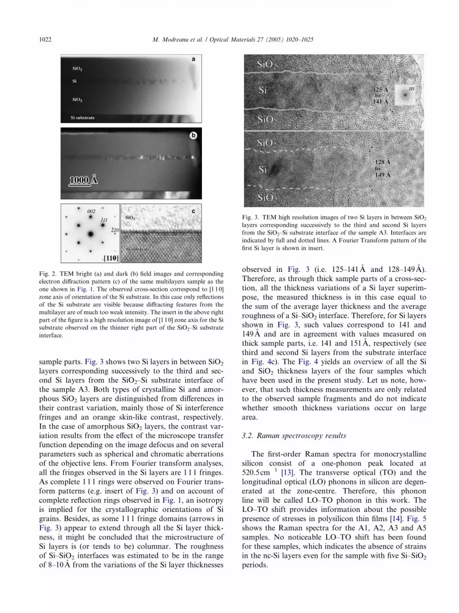
Fig. 3. TEM high resolution images of two Si layers in between SiO2
layers corresponding successively to the third and second Si layers
from the SiO2–Si substrate interface of the sample A3. Interfaces are
indicated by full and dotted lines. A Fourier Transform pattern of the
first Si layer is shown in insert.
Fig. 2. TEM bright (a) and dark (b) field images and corresponding
electron diffraction pattern (c) of the same multilayers sample as the
one shown in Fig. 1. The observed cross-section correspond to [110]
zone axis of orientation of the Si substrate. In this case only reflections
of the Si substrate are visible because diffracting features from the
multilayer are of much too weak intensity. The insert in the above right
part of the figure is a high resolution image of [110] zone axis for the Si
substrate observed on the thinner right part of the SiO2–Si substrate
interface.
1022 M. Modreanu et al. / Optical Materials 27 (2005) 1020–1025
sample parts. Fig. 3 shows two Si layers in between SiO2
layers corresponding successively to the third and sec-
ond Si layers from the SiO2–Si substrate interface of
the sample A3. Both types of crystalline Si and amor-
phous SiO2 layers are distinguished from differences in
their contrast variation, mainly those of Si interference
fringes and an orange skin-like contrast, respectively.
In the case of amorphous SiO2 layers, the contrast var-
iation results from the effect of the microscope transferfunction depending on the image defocus and on several
parameters such as spherical and chromatic aberrations
of the objective lens. From Fourier transform analyses,
all the fringes observed in the Si layers are 111 fringes.
As complete 111 rings were observed on Fourier trans-
form patterns (e.g. insert of Fig. 3) and on account of
complete reflection rings observed in Fig. 1, an isotropy
is implied for the crystallographic orientations of Sigrains. Besides, as some 111 fringe domains (arrows in
Fig. 3) appear to extend through all the Si layer thick-
ness, it might be concluded that the microstructure of
Si layers is (or tends to be) columnar. The roughness
of Si–SiO2 interfaces was estimated to be in the range
of 8–10A from the variations of the Si layer thicknesses
observed in Fig. 3 (i.e. 125–141A and 128–149A).
Therefore, as through thick sample parts of a cross-sec-
tion, all the thickness variations of a Si layer superim-
pose, the measured thickness is in this case equal to
the sum of the average layer thickness and the average
roughness of a Si–SiO2 interface. Therefore, for Si layersshown in Fig. 3, such values correspond to 141 and
149A and are in agreement with values measured on
thick sample parts, i.e. 141 and 151A, respectively (see
third and second Si layers from the substrate interface
in Fig. 4c). The Fig. 4 yields an overview of all the Si
and SiO2 thickness layers of the four samples which
have been used in the present study. Let us note, how-
ever, that such thickness measurements are only relatedto the observed sample fragments and do not indicate
whether smooth thickness variations occur on large
area.
3.2. Raman spectroscopy results
The first-order Raman spectra for monocrystalline
silicon consist of a one-phonon peak located at520.5cm�1 [13]. The transverse optical (TO) and the
longitudinal optical (LO) phonons in silicon are degen-
erated at the zone-centre. Therefore, this phonon
line will be called LO–TO phonon in this work. The
LO–TO shift provides information about the possible
presence of stresses in polysilicon thin films [14]. Fig. 5
shows the Raman spectra for the A1, A2, A3 and A5
samples. No noticeable LO–TO shift has been foundfor these samples, which indicates the absence of strains
in the nc-Si layers even for the sample with five Si–SiO2
periods.
Fig. 4. TEM bright field images of [110] zone axis cross-sections of the four nc-Si/SiO2 samples (a-A1, b-A2, c-A3 and d-A5) used in the present
study.
480 500 520 540 5600
100
200
300
400
500
600
I [a.
u.]
Wavenumber [cm-1]
A1
A2A3
A5
Fig. 5. Raman spectra for the samples A1, A2, A3 and A5. The 514nm
laser power was kept at 5mW in order to avoid heating of the samples.
350 375 400 425 450 475 500 5250
300
600
900
1200
PL (a
.u.)
Wavelength (nm)
280K
22K
100K
Fig. 6. Temperature dependence of the PL spectra for sample A1 (one
period nc-Si/SiO2). The dash and the dash-dot lines correspond to two
of the three-Gaussians deconvolution of the 22 K PL spectrum.
M. Modreanu et al. / Optical Materials 27 (2005) 1020–1025 1023
3.3. PL results
Fig. 6 shows the temperature dependence of PL spec-
tra for sample A1 (one period nc-Si/SiO2) obtained
using the excitation of the CW 325nm He–Cd laser.
The 22 K PL spectrum can be deconvoluted with three
Gaussians: one violet PL band centred at 409nm (see
the dash line in Fig. 6), and two blue PL bands, one cen-
tred at 436nm (see dash-dot line in Fig. 6) and the sec-
ond blue band centred at 485nm (not shown in Fig. 6).When the temperature increases from 22K to 280K the
PL spectra are red-shifted and the violet PL band cen-
tred at 405nm is quenched. There is only a slight de-
crease in the PL intensity of the blue band centred at
435nm when the room temperature is reached inside
the cryostat.
Figs. 7 and 8 show the temperature dependence of the
PL spectra for the sample A2 (two periods nc-Si/SiO2)
and A5 (five periods nc-Si/SiO2). It can be observed that
the PL intensity for sample A2 and A5 increases with the
number of nc-Si/SiO2 periods and red-shifts as the tem-
perature increases. When compared to sample A1, the
violet band is now centred at 411nm and the first blue
band becomes much larger and centred at 442nm. Thesecond blue band (485nm for sample A1 see Fig. 6) is
not present, probably being obscured by the first one.
A new ultraviolet band appears for sample A2 and A5
centred at 390nm. This band becomes very week at
room temperature (see Figs. 7 and 8).

350 375 400 425 450 475 500 525
2000
4000
6000
8000
10000
12000
14000
16000
18000PLE=325nm
PL (a
.u.)
Wavelength (nm)
280K
200K
100K
22K
Fig. 7. Temperature dependence of the PL spectra for sample A2 (two
periods nc-Si/SiO2).
350 375 400 425 450 475 500 525
5000
10000
15000
20000
25000 PLE=325nm
PL (a
.u.)
Wavelength (nm)
22K
100K
200K
280K
Fig. 8. Temperature dependence of the PL spectra for sample A5 (five
periods nc-Si/SiO2).
1024 M. Modreanu et al. / Optical Materials 27 (2005) 1020–1025
The origin of light emission in nc-Si is still under de-bate. Among the different mechanisms proposed for the
radiative recombination processes the most likely ones
are related to the direct band-to-band recombination
(usually named ‘‘quantum confinement models’’-QCM,
because the emission features strongly depend on the
size of the nanostructures [15]) and the exciton recombi-
nation via interface luminescent levels (usually called
‘‘surface recombination models’’-SRM [16]). The originof violet–blue light in Si/SiO2 multilayers is unclear. As
the TEM results showed that the nc-Si layer appeared to
be constituted of grains of greater than 100A, the QCM
cannot be used to explain the violet–blue light emission
from the samples investigated in this work. The rough-
ness of Si–SiO2 interfaces is estimated from TEM meas-
urements in the range of 8–10A so is not expected to
have a major contribution to the light emission mecha-nism. The Raman results have demonstrated the absence
of strains in the nc-Si layer so strain effects can also be
ruled out. Recently Wu [17] have reported a blue dou-
ble-peak PL centred around 416nm and 437nm in a
number of Si nanostructures and they concluded that
Si vacancies in silicon nanocrystals are responsible for
the blue light emission. Their conclusion is in agree-
ments with our findings which ruled out quantum con-
finements and surface roughness contributions to the
blue light emission.The origin of violet–blue light in Si/SiO2 multilayer remains unclear and further investiga-
tions are required in order to elucidate the emission
mechanism in this part of the spectrum.
4. Conclusions
In summary, a new approach was used for obtainingefficient light emission from nc-Si/SiO2 multilayer by
employing a technology compatible with the one used
for Si ICs. This approach involved the use of two stand-
ard CMOS processes, namely LPCVD and APCVD and
at temperatures as low as 625 �C.The HRTEM analysis revealed a columnar structure,
with an average grain size of 150A for the silicon layers
and smooth Si–SiO2 interfaces. Raman measurementsshowed the absence of stress in the nc-Si layers.
An intense room temperature blue light emission lo-
cated at 440nm can be clearly observed in nc-Si/SiO2
multilayers. The PL blue band is red-shifted and its
intensity increases with the increase of the number of
nc-Si/SiO2 periods. The origin of blue light in Si/SiO2
multilayers can be related to the presence of Si vacancies
within the nanocrystals grains.
Acknowledgement
This work was partial supported by Enterprise Ire-
land grant IF/2002/624.
References
[1] L.T. Canham, Appl. Phys. Lett. 57 (1990) 1046.
[2] A.G. Gullis, L.T. Canham, G.M. Williams, P.W. Smith, O.D.
Dosser, J. Appl. Phys. 75 (1994) 493.
[3] T. Shimizu-Iwayama, K. Fujita, S. Nakao, et al., J. Appl. Phys.
75 (1994) 7779.
[4] S. Hayashi, T. Nagareda, Y. Kanzawa, K. Yamamoto, Jpn. J.
Appl. Phys. 32 (1993) 3840.
[5] C. Ternon, F. Gourbilleau, C. Dufour, J.L. Doualan, B. Garrido,
J. Lumines. 99 (2002) 361.
[6] Z. Ma, L. Wang, K. Chen, W. Li, L. Zhang, Y. Bao, X. Wang, J.
Xu, X. Huang, D. Feng, J. Non-Cryst. Solids 299–302 (2002) 648.
[7] M. Modreanu, M. Gartner, E. Aperathitis, N. Tomozeiu, M.
Androulidaki, D. Cristea, P. Hurley, Physica E 16 (2003) 461.
[8] H. Nishikawa, E. Watanabe, D. Ito, M. Takiyama, A. Liki, Y.
Ohki, J. Appl. Phys. 78 (1995) 842.
[9] Y. Kanemitsu, T. Futagi, T. Matsumoto, H. Mimura, Phys. Rev.
B 49 (1994) 14723.
[10] D.J. Lockwood, Z.H. Lu, J.M. Baribeau, Phys. Rev. Lett. 76
(1996) 539.

M. Modreanu et al. / Optical Materials 27 (2005) 1020–1025 1025
[11] S. Nihonyanagi, K. Nishimoto, Y. Kanemitsu, J. Non-Cryst.
Solids 299–302 (2002) 1095.
[12] P. Photopoulos, A.G. Nassiopoulou, D.N. Kouvatsos, A. Trav-
los, Mater. Sci. Eng. B 69–70 (2000) 345.
[13] A. Zwick, R. Carles, Phys. Rev. B 48 (1993) 6024.
[14] E. Anastassakis, J. Appl. Phys. 86 (1999) 249.
[15] S. Guha, M.D. Pace, D.N. Dunn, I.L. Singer, Appl. Phys. Lett.
70 (1997) 1207.
[16] Y. Kanemitsu, S. Okamoto, Phys. Rev. B 56 (1997) R1696.
[17] X.L. Wu, S.J. Xiong, G.G. Siu, G.S. Huang, Y.F. Mei, Z.Y.
Zhang, S.S. Deng, C. Tang, Phys. Rev. Lett. 91 (2003)
157402-1.
Related Documents