Characterisation of L-band Differential Low Noise Amplifiers by David Schalk Van der Merwe Prinsloo Thesis presented in partial fulfilment of the requirements for the degree of Master of Science in Engineering at the Faculty of Engineering, Stellenbosch University Supervisors: Prof. Petrie Meyer Department of Electrical and Electronic Engineering Dr. Dirk de Villiers Department of Electrical and Electronic Engineering December 2011

Welcome message from author
This document is posted to help you gain knowledge. Please leave a comment to let me know what you think about it! Share it to your friends and learn new things together.
Transcript
Characterisation of L-band Differential Low Noise Amplifiers
by
David Schalk Van der Merwe Prinsloo
Thesis presented in partial fulfilment of the requirements for the degree ofMaster of Science in Engineering
at the Faculty of Engineering, Stellenbosch University
Supervisors:
Prof. Petrie Meyer
Department of Electrical and Electronic Engineering
Dr. Dirk de Villiers
Department of Electrical and Electronic Engineering
December 2011
Declaration
By submitting this thesis electronically, I declare that the entirety of the work contained therein is my own,
original work, that I am the sole author thereof (save to the extent explicitly otherwise stated), that reproduction
and publication thereof by Stellenbosch University will not infringe any third party rights and that I have not
previously in its entirety or in part submitted it for obtaining any qualification.
Date: December 2011
Copyright © 2011 Stellenbosch University
All rights reserved.
i
Stellenbosch University http://scholar.sun.ac.za
Abstract
Keywords - Noise, Noise Parameters, Correlation Matrix, Scattering Parameters, Multi-port Network, Mixed-
mode, Hybrid Coupler , Differential Low Noise Amplifier (dLNA), Low Noise Amplifier (LNA), Noise mea-
surement, Differential Noise Figure, Noise Figure.
This thesis addresses the complications that are encountered when characterising the performance of diffe-
rential microwave LNAs. The predominant sources of noise in electronic circuits are introduced and equivalent
two-port noise models for active devices are derived. Correlation between noise generators are defined by
means of the noise correlation matrix and existing network theory is adapted to include noise analysis of two-
port and multi-port networks. Mixed-mode scattering parameters are introduced in order to define the signal
performance of differential and common-mode propagation in multi-port networks and, by applying the same
theory, the mixed-mode correlation matrix for a three-port dLNA is derived. Furthermore, an expression is deri-
ved for de-embedding the differential noise figure of a three-port dLNA using two single ended measurements.
Two dLNA designs, both incorporating wideband 180-Hybrid ring couplers, are discussed and the differential
signal and noise performance of the dLNAs are compared to that of their constituent single ended LNAs.
ii
Stellenbosch University http://scholar.sun.ac.za
Opsomming
Sleutelwoorde - Ruis, Ruisparameters, Korrelasiematriks, S-parameters, Multipoortnetwerke , Gemengde-modus,
Differensiaalkoppelaar , Differensiële Laeruis Versterker, Laeruis Versterker, Ruismeting, Differensiäleruissy-
fer, Ruissyfer.
Hierdie tesis behandel die komplikasies wat ontwerpers in die gesig staar tydens die karakterisering van mi-
krogolf differensiële laeruis versterkers. Die hoof ruisbronne in stroombane word bespreek en ekwivalente
tweepoortnetwerkmodelle vir aktiewe toestelle word afgelei. Korrelasie tussen ruisbronne word gedefnieer
deur middel van ruiskorrelasiematrikse en bestaande tweepoort- en multipoort-netwerkteorie word aangepas
om ruismodelle in te sluit. Weens die feit dat differensiële- en gemene-wyse voortplanting van seine voorkom
in multipoortnetwerke word gemengde-modus S-parameters behandel. Dieselfde teorie maak dit vervolgens
moontlik om die gemengde-modus ruiskorrelasiematriks van ’n drie-poort differensiële laeruis versterker af
te lei. Verder word daar ’n wyse voorgestel waarmee die differensiëleruissyfer van ’n drie-poort differen-
siële laeruis versterker vanuit twee enkel ruissyfermetings bereken kan word. Twee differensiële laeruis vers-
terker ontwerpe, waarvan beide wyeband 180-differensiaalkoppelaars implementeer, word bespreek en die
differensiëlesein- asook die differensiëleruis-werking word vergelyk met die werking van die omsluite ongeba-
lanseerde laeruis versterkers.
iii
Stellenbosch University http://scholar.sun.ac.za
Acknowledgements
• Prof. Petrie Meyer and Dr. Dirk de Villiers, for their invaluable guidance and advice throughout the
project.
• Prof. Keith Palmer and Prof. PW van der Walt, for the insightful discussions during the early stages of
the project.
• Wessel Croukamp, Wynand van Eeden and Ashley Cupido, for their patience and expertise that made it
possible to bring my designs to life.
• Shamim, Sunelle, Madele, David, Phillip, and Theunis, for making Van, Werner, Charlie and myself feel
right at home in Stellenbosch.
• My parents, for never ceasing to believe in me.
• My brother, for administrating my life when it seemed that I had forgotten how.
• My friends, for keeping my life in balance throughout the project.
• My cousin Rachelle, for helping me keep perspective at all times and celebrating each accomplishment
with me.
• The NRF and SKA South Africa for funding this research.
iv
Stellenbosch University http://scholar.sun.ac.za
"Like diseases,
noise is never eliminated,
just prevented, cured, or endured,
depending on its nature, seriousness,
and the costs/difficulty of treating it."
- D. H. Sheingold -
v
Stellenbosch University http://scholar.sun.ac.za
Table of Contents
List of Figures ix
List of Tables xiii
List of Acronyms xiv
1 Introduction 11.1 Background . . . . . . . . . . . . . . . . . . . . . . . . . . . . . . . . . . . . . . . . . . . . 2
1.1.1 SKA Telescope . . . . . . . . . . . . . . . . . . . . . . . . . . . . . . . . . . . . . . 2
1.1.2 SKA Pathfinders . . . . . . . . . . . . . . . . . . . . . . . . . . . . . . . . . . . . . 3
1.1.3 Differential Low Noise Amplifiers . . . . . . . . . . . . . . . . . . . . . . . . . . . . 4
1.2 Objectives . . . . . . . . . . . . . . . . . . . . . . . . . . . . . . . . . . . . . . . . . . . . . 4
1.3 Overview . . . . . . . . . . . . . . . . . . . . . . . . . . . . . . . . . . . . . . . . . . . . . 5
2 Noise Circuit Analysis 62.1 Noise Generators . . . . . . . . . . . . . . . . . . . . . . . . . . . . . . . . . . . . . . . . . 7
2.1.1 Shot Noise . . . . . . . . . . . . . . . . . . . . . . . . . . . . . . . . . . . . . . . . 7
2.1.2 Thermal Noise . . . . . . . . . . . . . . . . . . . . . . . . . . . . . . . . . . . . . . 8
2.1.3 Other Sources of Noise . . . . . . . . . . . . . . . . . . . . . . . . . . . . . . . . . . 9
2.2 Noise Circuit Models for Active Devices . . . . . . . . . . . . . . . . . . . . . . . . . . . . . 10
2.2.1 Bipolar Junction Transistors . . . . . . . . . . . . . . . . . . . . . . . . . . . . . . . 10
2.2.2 Field Effect Transistors . . . . . . . . . . . . . . . . . . . . . . . . . . . . . . . . . . 14
2.3 Noise Parameters . . . . . . . . . . . . . . . . . . . . . . . . . . . . . . . . . . . . . . . . . 18
2.3.1 Equivalent two-port Noise Parameters . . . . . . . . . . . . . . . . . . . . . . . . . . 18
2.3.2 Noise Parameters of a Bipolar Junction Transistor . . . . . . . . . . . . . . . . . . . . 20
2.3.2.1 Motchenbacher’s Noise Model . . . . . . . . . . . . . . . . . . . . . . . . 20
2.3.2.2 Voinigescu’s Noise Model . . . . . . . . . . . . . . . . . . . . . . . . . . . 21
2.3.3 Noise Parameters of Field Effect Transistors . . . . . . . . . . . . . . . . . . . . . . . 23
2.4 Experimental Verification of Noise Models . . . . . . . . . . . . . . . . . . . . . . . . . . . 25
2.4.1 Bipolar Junction Transistor Amplifier Design . . . . . . . . . . . . . . . . . . . . . . 25
2.4.1.1 Motchenbacher’s noise model . . . . . . . . . . . . . . . . . . . . . . . . . 26
2.4.1.2 Voinigescu’s noise model . . . . . . . . . . . . . . . . . . . . . . . . . . . 27
2.4.2 Field Effect Transistors - Pospieszalski’s Noise Model . . . . . . . . . . . . . . . . . 29
vi
Stellenbosch University http://scholar.sun.ac.za
TABLE OF CONTENTS vii
2.5 Conclusion . . . . . . . . . . . . . . . . . . . . . . . . . . . . . . . . . . . . . . . . . . . . 30
3 Noise Correlation Matrix 313.1 Definition of the Correlation Matrix . . . . . . . . . . . . . . . . . . . . . . . . . . . . . . . 32
3.2 Correlation matrix in terms of Equivalent two-port Noise Parameters . . . . . . . . . . . . . . 34
3.3 Correlation matrix in terms of Noise Generators . . . . . . . . . . . . . . . . . . . . . . . . . 37
3.4 Multi-Port Networks . . . . . . . . . . . . . . . . . . . . . . . . . . . . . . . . . . . . . . . 39
3.5 Conclusion . . . . . . . . . . . . . . . . . . . . . . . . . . . . . . . . . . . . . . . . . . . . 44
4 Transmission Line Theory 454.1 Generalized Scattering Parameters . . . . . . . . . . . . . . . . . . . . . . . . . . . . . . . . 45
4.2 Mixed-Mode Scattering Parameters . . . . . . . . . . . . . . . . . . . . . . . . . . . . . . . 47
4.2.1 Coupled Transmission lines: Even and Odd mode Propagation . . . . . . . . . . . . . 47
4.2.2 Coupled Transmission lines: Differential- and Common-mode Signals . . . . . . . . . 49
4.3 Mixed-mode Scattering Parameters derived from General Scattering Parameters . . . . . . . . 51
4.4 Conclusion . . . . . . . . . . . . . . . . . . . . . . . . . . . . . . . . . . . . . . . . . . . . 54
5 Noise Figure Measurement 555.1 Linear Two-port Devices . . . . . . . . . . . . . . . . . . . . . . . . . . . . . . . . . . . . . 55
5.1.1 Y-factor Measurement . . . . . . . . . . . . . . . . . . . . . . . . . . . . . . . . . . 56
5.1.2 Measurement Accuracy Improvement . . . . . . . . . . . . . . . . . . . . . . . . . . 57
5.1.3 Investigating Accuracy Improvement . . . . . . . . . . . . . . . . . . . . . . . . . . 59
5.1.4 Alternative Measurement Techniques . . . . . . . . . . . . . . . . . . . . . . . . . . 65
5.1.4.1 ’Cold-source’ Measurement . . . . . . . . . . . . . . . . . . . . . . . . . . 65
5.1.4.2 Improved Y-factor Measurement . . . . . . . . . . . . . . . . . . . . . . . 66
5.2 Differential Devices . . . . . . . . . . . . . . . . . . . . . . . . . . . . . . . . . . . . . . . . 68
5.2.1 De-embedding the Differential Noise Figure using Baluns . . . . . . . . . . . . . . . 68
5.2.2 Deriving the Mixed-Mode Noise Correlation Matrix from Noise Figure Measurements 71
5.2.3 De-embedding the Differential Noise Figure without the use of Baluns . . . . . . . . . 73
5.3 Extracting the Differential noise factor . . . . . . . . . . . . . . . . . . . . . . . . . . . . . . 76
5.4 Experimental Verification of Differential noise factor Extraction . . . . . . . . . . . . . . . . 78
5.4.1 Case 1: Equal Gains with Different Noise Contribution . . . . . . . . . . . . . . . . . 79
5.4.2 Case 2: Equal Noise Contribution with Different Gains . . . . . . . . . . . . . . . . . 79
5.5 Conclusion . . . . . . . . . . . . . . . . . . . . . . . . . . . . . . . . . . . . . . . . . . . . 81
6 Differential Low Noise Amplifier Design and Noise Figure Verification 826.1 Planar Four-Port Couplers . . . . . . . . . . . . . . . . . . . . . . . . . . . . . . . . . . . . 83
6.1.1 The 180-Hybrid Coupler . . . . . . . . . . . . . . . . . . . . . . . . . . . . . . . . 85
6.1.1.1 Even and Odd Mode Analysis . . . . . . . . . . . . . . . . . . . . . . . . . 86
6.1.1.2 Narrowband Design . . . . . . . . . . . . . . . . . . . . . . . . . . . . . . 89
6.1.2 Wideband Reduced Size 180-Hybrid Coupler Designs . . . . . . . . . . . . . . . . . 91
6.1.3 Finite Ground Coplanar Waveguide 180-Hybrid Ring Coupler Design . . . . . . . . 93
Stellenbosch University http://scholar.sun.ac.za
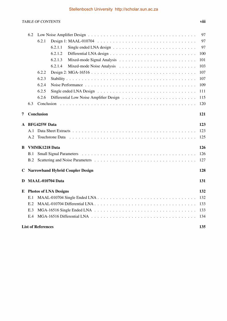
TABLE OF CONTENTS viii
6.2 Low Noise Amplifier Design . . . . . . . . . . . . . . . . . . . . . . . . . . . . . . . . . . . 97
6.2.1 Design 1: MAAL-010704 . . . . . . . . . . . . . . . . . . . . . . . . . . . . . . . . 97
6.2.1.1 Single ended LNA design . . . . . . . . . . . . . . . . . . . . . . . . . . . 97
6.2.1.2 Differential LNA design . . . . . . . . . . . . . . . . . . . . . . . . . . . . 100
6.2.1.3 Mixed-mode Signal Analysis . . . . . . . . . . . . . . . . . . . . . . . . . 101
6.2.1.4 Mixed-mode Noise Analysis . . . . . . . . . . . . . . . . . . . . . . . . . 103
6.2.2 Design 2: MGA-16516 . . . . . . . . . . . . . . . . . . . . . . . . . . . . . . . . . . 107
6.2.3 Stability . . . . . . . . . . . . . . . . . . . . . . . . . . . . . . . . . . . . . . . . . . 107
6.2.4 Noise Performance . . . . . . . . . . . . . . . . . . . . . . . . . . . . . . . . . . . . 109
6.2.5 Single ended LNA Design . . . . . . . . . . . . . . . . . . . . . . . . . . . . . . . . 111
6.2.6 Differential Low Noise Amplifier Design . . . . . . . . . . . . . . . . . . . . . . . . 115
6.3 Conclusion . . . . . . . . . . . . . . . . . . . . . . . . . . . . . . . . . . . . . . . . . . . . 120
7 Conclusion 121
A BFG425W Data 123A.1 Data Sheet Extracts . . . . . . . . . . . . . . . . . . . . . . . . . . . . . . . . . . . . . . . . 123
A.2 Touchstone Data . . . . . . . . . . . . . . . . . . . . . . . . . . . . . . . . . . . . . . . . . 125
B VMMK1218 Data 126B.1 Small Signal Parameters . . . . . . . . . . . . . . . . . . . . . . . . . . . . . . . . . . . . . 126
B.2 Scattering and Noise Parameters . . . . . . . . . . . . . . . . . . . . . . . . . . . . . . . . . 127
C Narrowband Hybrid Coupler Design 128
D MAAL-010704 Data 131
E Photos of LNA Designs 132E.1 MAAL-010704 Single Ended LNA . . . . . . . . . . . . . . . . . . . . . . . . . . . . . . . . 132
E.2 MAAL-010704 Differential LNA . . . . . . . . . . . . . . . . . . . . . . . . . . . . . . . . . 133
E.3 MGA-16516 Single Ended LNA . . . . . . . . . . . . . . . . . . . . . . . . . . . . . . . . . 133
E.4 MGA-16516 Differential LNA . . . . . . . . . . . . . . . . . . . . . . . . . . . . . . . . . . 134
List of References 135
Stellenbosch University http://scholar.sun.ac.za
List of Figures
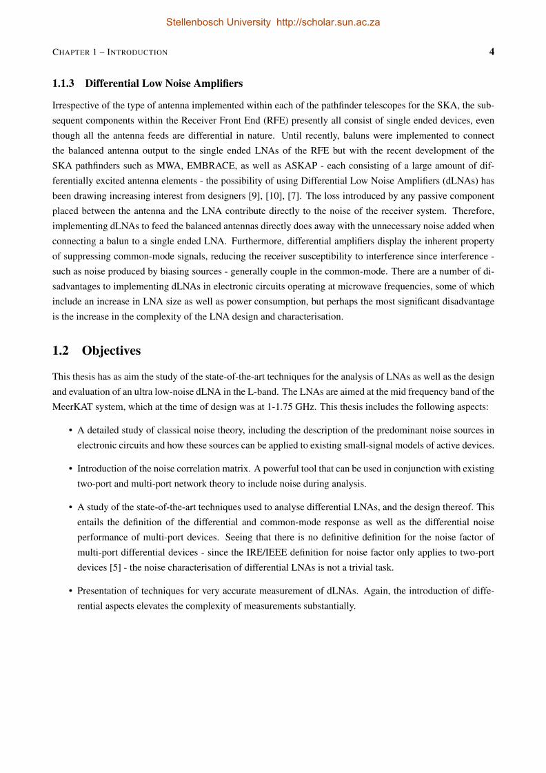
1.1 The proposed (a) layout of the SKA telescope illustrating (b) the three different antennas within the
core, from [1]. . . . . . . . . . . . . . . . . . . . . . . . . . . . . . . . . . . . . . . . . . . . . . 2
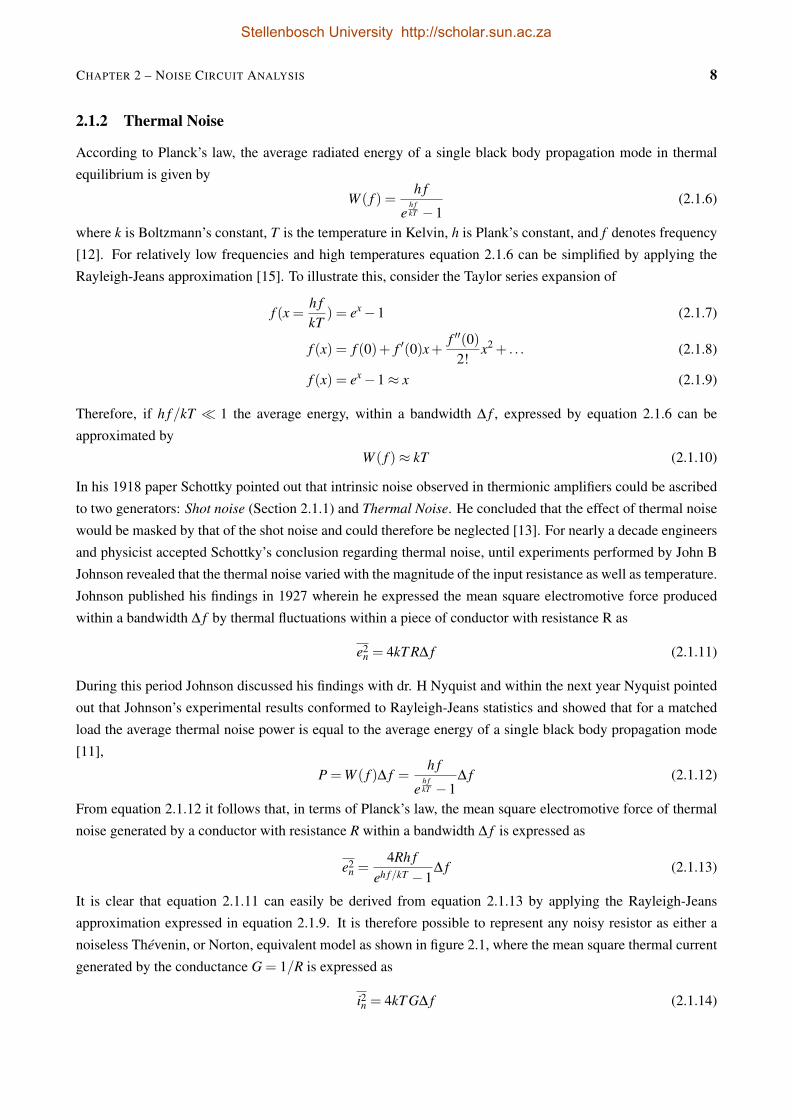
2.1 (a) Noisy Resistor, (b) Thevenin equivalent circuit, (c) Norton equivalent circuit. . . . . . . . . . 9
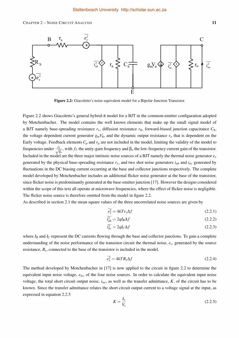
2.2 Giacoletto’s noise equivalent model for a Bipolar Junction Transistor. . . . . . . . . . . . . . . . 11
2.3 Equivalent noise sources connected to their associated noiseless BJT. . . . . . . . . . . . . . . . . 13
2.4 Noise model for FETs proposed by Van der Ziel. . . . . . . . . . . . . . . . . . . . . . . . . . . 14
2.5 Noise model for FETs proposed by Pospiezalski. . . . . . . . . . . . . . . . . . . . . . . . . . . 15
2.6 Admittance representation of a noisy HEMT. . . . . . . . . . . . . . . . . . . . . . . . . . . . . 16
2.7 Chain representation of a noisy HEMT. . . . . . . . . . . . . . . . . . . . . . . . . . . . . . . . 17
2.8 General noise equivalent model of an amplifier. . . . . . . . . . . . . . . . . . . . . . . . . . . . 20
2.9 Small signal noise equivalent circuit used for derivation of noise parameters. . . . . . . . . . . . . 21
2.10 Equivalent input noise as a function of collector current. . . . . . . . . . . . . . . . . . . . . . . 25
2.11 SPICE simulation of LNA circuit biased for minimum noise contribution. . . . . . . . . . . . . . 26
2.12 LNA circuit implementing Motchenbacher’s noise model. . . . . . . . . . . . . . . . . . . . . . . 27
2.13 Simulated output noise of Motchenbacher’s noise model. . . . . . . . . . . . . . . . . . . . . . . 27
2.14 LNA circuit diagram containing transistor S-parameters and calculated noise parameters. . . . . . 28
2.15 Simulated noise figure of the BJT noise models. . . . . . . . . . . . . . . . . . . . . . . . . . . . 28
2.16 Experimental verification of HEMT noise model. . . . . . . . . . . . . . . . . . . . . . . . . . . 30
3.1 Chain representation of a noisy two-port network. . . . . . . . . . . . . . . . . . . . . . . . . . . 34
3.2 Linear noise free two-port shorted at the input. . . . . . . . . . . . . . . . . . . . . . . . . . . . . 35
3.3 Noisy small signal model of a BJT. . . . . . . . . . . . . . . . . . . . . . . . . . . . . . . . . . . 37
3.4 Hybrid-pi model separated into two cascaded noise free two-port networks in admittance represen-
tation. . . . . . . . . . . . . . . . . . . . . . . . . . . . . . . . . . . . . . . . . . . . . . . . . . 38
3.5 n-Port network with m embedded active devices. . . . . . . . . . . . . . . . . . . . . . . . . . . . 39
3.6 Noise free multi-port network with internal equivalent noise sources. . . . . . . . . . . . . . . . . 39
3.7 Chain (a) and Admittance (b) two-port representations. . . . . . . . . . . . . . . . . . . . . . . . 40
3.8 Noise free multi-port network with only n external equivalent noise sources. . . . . . . . . . . . . 41
3.9 Noise free multi-port network with each port driven by a source. . . . . . . . . . . . . . . . . . . 42
4.1 Generalized multi-port network showing incident and reflected waves. . . . . . . . . . . . . . . . 46
4.2 Differential two-port network with coupled lines connected to the input and output of the DUT. . . 47
ix
Stellenbosch University http://scholar.sun.ac.za
LIST OF FIGURES x
4.3 Electric field lines showing (a) Even and (b) Odd mode propagation. . . . . . . . . . . . . . . . . 48
4.4 Symmetric, terminated, coupled transmission lines over a ground plane. . . . . . . . . . . . . . . 49
5.1 Graphical representation of the linear relationship between input noise temperature and output noise
power, from [2]. . . . . . . . . . . . . . . . . . . . . . . . . . . . . . . . . . . . . . . . . . . . . 55
5.2 Schematic representation of the Y-factor measurement setup. . . . . . . . . . . . . . . . . . . . . 56
5.3 Schematic representation of the noise figure measurement system. . . . . . . . . . . . . . . . . . 58
5.4 Input Standing Wave Ratio of the Agilent N8975A NFA with frequency. . . . . . . . . . . . . . . 58
5.5 Measurement calibration configurations implementing, (a) Attenuators, (b) Attenuators connected
to a pre-amplifier with a 10dB attenuator at the output, (c) Circulator. . . . . . . . . . . . . . . . . 59
5.6 Calibrated noise figures of 3dB and 6dB attenuator compared to noise source only. . . . . . . . . 60
5.7 Calibrated noise figures of 3dB and 10dB attenuators cascaded with a pre-amplifier - no internal
attenuation. . . . . . . . . . . . . . . . . . . . . . . . . . . . . . . . . . . . . . . . . . . . . . . 61
5.8 Calibrated noise figures of 3dB and 10dB attenuators cascaded with a pre-amplifier - internal atte-
nuation adjusted. . . . . . . . . . . . . . . . . . . . . . . . . . . . . . . . . . . . . . . . . . . . 61
5.9 LNA noise figure measured with noise source connected directly to DUT. . . . . . . . . . . . . . 62
5.10 LNA noise figure measured with a 3dB attenuator connected between the noise source and the DUT. 62
5.11 Calibrated noise figure with circulator compared to noise source only. . . . . . . . . . . . . . . . 63
5.12 Measured (a) insertion loss and (b) reflection coefficients of the circulator used during calibration. 63
5.13 Schematic representation of the noise figure (a) calibration setup and (b) measurement setup. . . . 64
5.14 Noise figure measured using circulators compared to simulated noise figure. . . . . . . . . . . . . 65
5.15 Cold source measurement system. . . . . . . . . . . . . . . . . . . . . . . . . . . . . . . . . . . 66
5.16 Source constellations used in cold source noise measurement. . . . . . . . . . . . . . . . . . . . . 66
5.17 Measurement system for improved Y-factor noise measurement, from [3]. . . . . . . . . . . . . . 67
5.18 Constellation of source reflections in a narrow bandwidth as seen by the DUT . . . . . . . . . . . 68
5.19 Differential amplifier connected to ideal input and output baluns, from [4]. . . . . . . . . . . . . . 69
5.20 Single ended measurement of the (a) power-splitting and (b) power-combining baluns. . . . . . . 70
5.21 Impedance representation of a noisy four-port network, from [5]. . . . . . . . . . . . . . . . . . . 71
5.22 Schematic representation of the differential LNA driven by a differential excitation. . . . . . . . . 74
5.23 Noise contribution of the LNA represented by two uncorrelated input referred noise sources. . . . 75
5.24 Equivalent thermal network representing the differential noise contribution of the LNA. . . . . . . 76
5.25 Single-ended noise figure measurement with ports 2 and 4 terminated. . . . . . . . . . . . . . . . 78
5.26 Single-ended noise figure measurement with ports 1 and 4 terminated. . . . . . . . . . . . . . . . 78
5.27 Simulated single-ended LNA. . . . . . . . . . . . . . . . . . . . . . . . . . . . . . . . . . . . . . 78
5.28 Simulated circuit schematic for differentially excited LNA. . . . . . . . . . . . . . . . . . . . . . 79
5.29 Comparing the extracted differential noise figure to the noise figure obtained from a differential
excitation. . . . . . . . . . . . . . . . . . . . . . . . . . . . . . . . . . . . . . . . . . . . . . . . 80
5.30 De-embedded differential noise figure validated. . . . . . . . . . . . . . . . . . . . . . . . . . . . 80
6.1 Two main topologies of differential amplifiers: (a) Balanced topology (b) and Differential topology. 82
6.2 Schematic representaion of a reciprocal four-port directional coupler. . . . . . . . . . . . . . . . . 83
6.3 Schematic representation of 180-Hybrid Coupler. . . . . . . . . . . . . . . . . . . . . . . . . . . 85
Stellenbosch University http://scholar.sun.ac.za
LIST OF FIGURES xi
6.4 Planar (a) 180-Hybrid Ring and (b) Tapered Coupled Line Coupler. . . . . . . . . . . . . . . . . 85
6.5 Symmetrical four-port network. . . . . . . . . . . . . . . . . . . . . . . . . . . . . . . . . . . . 86
6.6 (a) Even and odd mode analysis applied to hybrid ring coupler excited at Port 1, (b) Equivalent
two-port circuits for Even mode analysis, (c) and Odd mode analysis. . . . . . . . . . . . . . . . 87
6.7 (a) Even and odd mode analysis applied to Hybrid ring coupler excited at Port 4, (b) Equivalent
two-port circuits for Even mode analysis, (c) and Odd mode analysis. . . . . . . . . . . . . . . . 88
6.8 Transmission line model of narrowband hybrid ring coupler simulated in Microwave Office AWR. 89
6.9 S-parameters of ideal hybrid ring coupler transmission line model. . . . . . . . . . . . . . . . . . 89
6.10 Comparison of the phase difference at Ports 2 and 3 for an excitation at Port 4. . . . . . . . . . . . 90
6.11 Microstrip Hybrid ring coupler incorporating a coupled line phase inverter. . . . . . . . . . . . . . 91
6.12 Microstrip Back-to-Back Balun phase inverter. . . . . . . . . . . . . . . . . . . . . . . . . . . . . 92
6.13 Coplanar waveguide to Slotline Back-to-Back Balun phase inverter. . . . . . . . . . . . . . . . . 92
6.14 Uniplanar Coplanar Hybrid ring coupler with integrated CPW-Slotline Back-to-Back Balun. . . . 93
6.15 Finite Ground Coplanar waveguide phase inverter. . . . . . . . . . . . . . . . . . . . . . . . . . . 93
6.16 (a) Finite Ground Coplanar waveguide phase inverter and (b) through connection simulated in
AXIEM. . . . . . . . . . . . . . . . . . . . . . . . . . . . . . . . . . . . . . . . . . . . . . . . . 94
6.17 Simulated output phase comparison between FGCPW inverter and FGCPW through connection. . 94
6.18 FGCPW 180-Hybrid Ring coupler simulated in CST Microwave Studio. . . . . . . . . . . . . . 95
6.19 Simulated Return loss and Isolation of FGCPW Hybrid ring coupler. . . . . . . . . . . . . . . . . 95
6.20 Insertion loss of Input Ports 2 and 3 simulated at Difference Port 4. . . . . . . . . . . . . . . . . . 96
6.21 Simulated phase difference between Ports 2 and 3 for an excitation at Difference Port 4. . . . . . . 96
6.22 Schematic representation of the three-port differential LNA. . . . . . . . . . . . . . . . . . . . . 97
6.23 MAAL-010704 Single ended LNA circuit schematic. . . . . . . . . . . . . . . . . . . . . . . . . 97
6.24 MAAL-010704 Single ended LNA layout. . . . . . . . . . . . . . . . . . . . . . . . . . . . . . . 98
6.25 MAAL-010704 Single ended LNA layout simulated in MWO. . . . . . . . . . . . . . . . . . . . 98
6.26 Simulated (a) Gain and (b) Reflection Coefficients of MAAL-010704 Single ended LNA. . . . . . 99
6.27 MAAL-010704 Single ended LNA noise figure. . . . . . . . . . . . . . . . . . . . . . . . . . . . 99
6.28 Transition between Coplanar Waveguide with bottom ground plane to Finite Ground Coplanar Wa-
veguide without a bottom ground plane. . . . . . . . . . . . . . . . . . . . . . . . . . . . . . . . 100
6.29 Simulated (a) Insertion Loss and (b) Reflection Coefficients of CPW transition. . . . . . . . . . . 100
6.30 MAAL-010704 Differential LNA design layout. . . . . . . . . . . . . . . . . . . . . . . . . . . . 101
6.31 Three-port Differential LNA design simulated in MWO AWR using S-parameter and Noise para-
meter blocks. . . . . . . . . . . . . . . . . . . . . . . . . . . . . . . . . . . . . . . . . . . . . . 102
6.32 Simulated and measured (a) Gains and (b) Reflection Coefficients of the MAAL-010704 dLNA
design. . . . . . . . . . . . . . . . . . . . . . . . . . . . . . . . . . . . . . . . . . . . . . . . . . 103
6.33 Simulated and measured (a) Phase imbalance and (b) CMRR of the MAAL-010704 dLNA design. 103
6.34 Noisy Three-port network. . . . . . . . . . . . . . . . . . . . . . . . . . . . . . . . . . . . . . . 104
6.35 Differential noise figure and minimum differential noise figure calculated using mixed-mode ana-
lysis compared to simulated values. . . . . . . . . . . . . . . . . . . . . . . . . . . . . . . . . . 106
6.36 Simulated and measured (a) single ended and (b) de-embedded differential noise figure of the
MAAL-010704 dLNA design. . . . . . . . . . . . . . . . . . . . . . . . . . . . . . . . . . . . . 107
Stellenbosch University http://scholar.sun.ac.za
LIST OF FIGURES xii
6.37 General representation of two-port amplifier network. . . . . . . . . . . . . . . . . . . . . . . . . 107
6.38 Input Stability circle plotted in ΓS Plane. . . . . . . . . . . . . . . . . . . . . . . . . . . . . . . . 109
6.39 General two-port representation of amplifier with matching networks indicating the respective gain
terms. . . . . . . . . . . . . . . . . . . . . . . . . . . . . . . . . . . . . . . . . . . . . . . . . . 110
6.40 Constant Noise Figure (blue) and Gain (green) circles plotted in the ΓS plane. . . . . . . . . . . . 111
6.41 Single ended LNA biasing circuit schematic. . . . . . . . . . . . . . . . . . . . . . . . . . . . . . 111
6.42 Effect of loading resistors on device stability. . . . . . . . . . . . . . . . . . . . . . . . . . . . . 112
6.43 Ideal impedance tuners connected to the Biasing circuit used to determine optimum noise and
power match. . . . . . . . . . . . . . . . . . . . . . . . . . . . . . . . . . . . . . . . . . . . . . 112
6.44 Synthesised Input (a) and Output (b) lumped element matching networks. . . . . . . . . . . . . . 113
6.45 Circuit Schematic of the single ended LNA design. . . . . . . . . . . . . . . . . . . . . . . . . . 113
6.46 Layout of two matched single ended LNAs. . . . . . . . . . . . . . . . . . . . . . . . . . . . . . 114
6.47 Measured and simulated (a) Gain and (b) Input and Output Reflection Coefficients of the MGA-
16516 single ended LNA. . . . . . . . . . . . . . . . . . . . . . . . . . . . . . . . . . . . . . . . 115
6.48 Simulated and measured noise figure of single ended LNAs. . . . . . . . . . . . . . . . . . . . . 115
6.49 Single ended LNA coplanar layout simulated in MWO. . . . . . . . . . . . . . . . . . . . . . . . 116
6.50 PCB layout of Differential Low Noise Amplifier. . . . . . . . . . . . . . . . . . . . . . . . . . . 117
6.51 Measured and simulated (a) Gains and (b) CMRR of the MGA-16516 differential LNA. . . . . . . 117
6.52 Simulated (a) Input and (b) Output Reflection Coefficients of Differential LNA. . . . . . . . . . . 118
6.53 Simulated and measured (a) Amplitude and (b) Phase Imbalance of Differential LNA. . . . . . . . 119
6.54 Simulated Single Ended Noise Figure of Differential LNA. . . . . . . . . . . . . . . . . . . . . . 119
6.55 De-embedded Differential Noise Figure compared to the Noise Figure of the Single Ended LNA. . 120
C.1 CPW Hybrid coupler simulated in CST. . . . . . . . . . . . . . . . . . . . . . . . . . . . . . . . 128
C.2 Manufactured Hybrid coupler (a) Phase and (b) Amplitude imbalances compared to simulated results.129
C.3 Cross sections of (a) Etched and (b) Milled CPW transmission lines. . . . . . . . . . . . . . . . . 129
C.4 Simulated effective dielectric constant of etched and milled CPW transmission lines. . . . . . . . 130
Stellenbosch University http://scholar.sun.ac.za
List of Tables
3.1 Three representations of the correlation matrix. . . . . . . . . . . . . . . . . . . . . . . . . . . . 32
3.2 Transformation matrices for the three correlation matrix representations. . . . . . . . . . . . . . . 33
6.1 Description of MAAL-010704 single ended LNA design components . . . . . . . . . . . . . . . 98
6.2 Description of single ended LNA components . . . . . . . . . . . . . . . . . . . . . . . . . . . . 114
xiii
Stellenbosch University http://scholar.sun.ac.za
List of Acronyms
ASKAP Australian Square Kilometer Array Pathfinder
BJT Bipolar Junction Transistor
CMRR Common Mode Rejection Ratio
CPW Coplanar Waveguide
CST Computer Simulation Technology
DC Direct Current
dLNA Differential Low Noise Amplifier
DUT Device Under Test
EM Electromagnetic
EMBRACE Electronic Multi Beam Radio Astronomy ConcEpt
ENR Excess Noise Ratio
FET Field Effect Transistor
FGCPW Finite Ground Coplanar Waveguide
GaAs Gallium Arsenide
HEMT High Electron Mobility Transistor
JFET Junction Field Effect Transistor
LNA Low Noise Amplifier
LWA Long Wavelength Array
MESFET Metal Semiconductor Field Effect Transistor
MOSFET Metal Oxide Semiconductor Field Effect Transistor
MWA Murchison Widefield Array
xiv
Stellenbosch University http://scholar.sun.ac.za

CHAPTER 0 – LIST OF ACRONYMS xv
MWO Microwave Office
NFA Noise Figure Analyser
PAF Phased Array Feed
PCB Printed Circuit Board
pHEMT pseudomorphic High Electron Mobility Transistor
QFN Quad-Flat-Non-Lead
RFE Receiver Front End
S Scattering
SKA Square Kilometer Array
SMD Surface Mount Device
SWR Standing Wave Ratio
VNA Vector Network Analyser
WBSPF Wide-Band Single Pixel Feed
Stellenbosch University http://scholar.sun.ac.za

Chapter 1
Introduction
Everything radiates.
Be it a celestial or terrestrial body, all objects emit Electromagnetic (EM) energy that can be defined as either
thermal or non-thermal in nature. In order to gain a better understanding of the universe, astronomers study
both the thermal and non-thermal EM radiation of celestial bodies. As this radiation is normally at extremely
low power levels when it reaches Earth, radio astronomy systems have two critical system parameters which
determine their performance, namely receiving area and added noise. Together, these two aspects determine
the sensitivity of the receivers, where
Sensitivity =Aperture Area
System Temperature(1.0.1)
The proposed Square Kilometer Array (SKA) is intended to have the largest receiving area of any radio teles-
cope in the world. This large collecting aperture is however of little use if the receivers following the antenna
adds so much noise that the received signals cannot be identified. To ensure a sensitive system, it is therefore
imperative that extremely Low Noise Amplifiers (LNAs) are used in the very first stage of the receiving chain
since their noise contribute directly to the system temperature. This thesis focusses on the theory and design of
these LNAs.
1
Stellenbosch University http://scholar.sun.ac.za
CHAPTER 1 – INTRODUCTION 2
1.1 Background
1.1.1 SKA Telescope
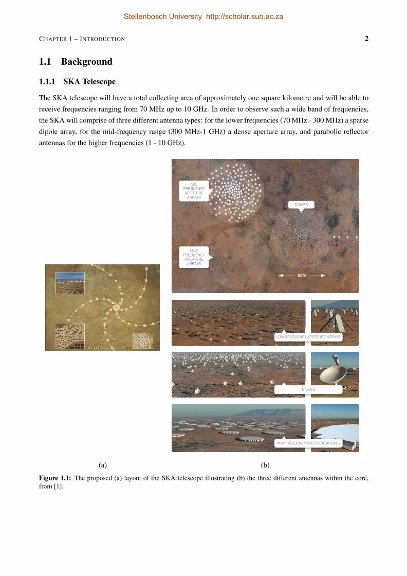
The SKA telescope will have a total collecting area of approximately one square kilometre and will be able to
receive frequencies ranging from 70 MHz up to 10 GHz. In order to observe such a wide band of frequencies,
the SKA will comprise of three different antenna types: for the lower frequencies (70 MHz - 300 MHz) a sparse
dipole array, for the mid-frequency range (300 MHz-1 GHz) a dense aperture array, and parabolic reflector
antennas for the higher frequencies (1 - 10 GHz).
MID FREQUENCY APERTURE
ARRAYS
LOW FREQUENCY APERTURE
ARRAYS
LOW FREQUENCY APERTURE ARRAYS
DISHES
MID FREQUENCY APERTURE ARRAYS
DISHES
5KM
(a) (b)
Figure 1.1: The proposed (a) layout of the SKA telescope illustrating (b) the three different antennas within the core,from [1].
Stellenbosch University http://scholar.sun.ac.za

CHAPTER 1 – INTRODUCTION 3
The proposed layout of the SKA is shown in figure 1.1(a). It comprises of a central core, approximately 15 to 20
kilometres in diameter, containing the sparse and dense aperture arrays as well as almost half of the parabolic
reflector antennas, as illustrated in figure 1.1(b). The remainder of the parabolic reflectors are situated in sub-
stations spiralling outward to a distance of at least 3000 kilometres from the core site. This will allow for
extremely long baselines and therefore excellent resolution. Two sites, Southern Africa and Australia, have
been short-listed to host the SKA and both countries are currently working on SKA pathfinders. South Africa
is building MeerKAT [6], a telescope that will consist of 64, 13.5 meter diameter Gregorian Offset reflector
antennas and Australia is constructing the Australian Square Kilometer Array Pathfinder (ASKAP) [7] that will
consist of 36, single reflector antennas, each with a diameter of 12 meters.
1.1.2 SKA Pathfinders
Apart from the two precursor telescopes being built on the candidate sites - MeerKAT and ASKAP - institutions
around the globe are building other SKA pathfinders concentrating primarily on the sparse and dense aperture
arrays. These include, amongst others [8]
• Murchison Widefield Array (MWA) - A phased array built in Australia, consisting of 16 dual-polarization
dipoles operating over 80 - 300 MHz.
• Electronic Multi Beam Radio Astronomy ConcEpt (EMBRACE) - An aperture array concept being built
in the Netherlands that will consist of an array of just over 20000 differentially fed antenna elements
(possibly Vivaldi antennas) that conduct observations from 100 MHz up to 2 GHz.
• Long Wavelength Array (LWA) - Developed in the state of New Mexico, the LWA will consist of 53
phased array stations, each with 256 pairs of dipole type antennas, and operate over the frequency range
of 10 - 80 MHz.
Two vastly different types of feeds are being considered for the reflector antennas of the precursor telescopes.
MeerKAT will implement Wide-Band Single Pixel Feeds (WBSPFs) consisting of two dual-polarization dipoles
and will support three receivers operating at 0.58 - 1.1015 GHz, 1 - 1.75 GHz, and 8 - 14.5 GHz. On the other
hand ASKAP is investigating the implementation of Phased Array Feeds (PAFs) that consist of an array of more
than 200 antenna elements, presently operating at a frequency range of 0.7 - 1.8 GHz with plans to extend the
operating range to 0.5 - 10 GHz or even higher.
Stellenbosch University http://scholar.sun.ac.za
CHAPTER 1 – INTRODUCTION 4
1.1.3 Differential Low Noise Amplifiers
Irrespective of the type of antenna implemented within each of the pathfinder telescopes for the SKA, the sub-
sequent components within the Receiver Front End (RFE) presently all consist of single ended devices, even
though all the antenna feeds are differential in nature. Until recently, baluns were implemented to connect
the balanced antenna output to the single ended LNAs of the RFE but with the recent development of the
SKA pathfinders such as MWA, EMBRACE, as well as ASKAP - each consisting of a large amount of dif-
ferentially excited antenna elements - the possibility of using Differential Low Noise Amplifiers (dLNAs) has
been drawing increasing interest from designers [9], [10], [7]. The loss introduced by any passive component
placed between the antenna and the LNA contribute directly to the noise of the receiver system. Therefore,
implementing dLNAs to feed the balanced antennas directly does away with the unnecessary noise added when
connecting a balun to a single ended LNA. Furthermore, differential amplifiers display the inherent property
of suppressing common-mode signals, reducing the receiver susceptibility to interference since interference -
such as noise produced by biasing sources - generally couple in the common-mode. There are a number of di-
sadvantages to implementing dLNAs in electronic circuits operating at microwave frequencies, some of which
include an increase in LNA size as well as power consumption, but perhaps the most significant disadvantage
is the increase in the complexity of the LNA design and characterisation.
1.2 Objectives
This thesis has as aim the study of the state-of-the-art techniques for the analysis of LNAs as well as the design
and evaluation of an ultra low-noise dLNA in the L-band. The LNAs are aimed at the mid frequency band of the
MeerKAT system, which at the time of design was at 1-1.75 GHz. This thesis includes the following aspects:
• A detailed study of classical noise theory, including the description of the predominant noise sources in
electronic circuits and how these sources can be applied to existing small-signal models of active devices.
• Introduction of the noise correlation matrix. A powerful tool that can be used in conjunction with existing
two-port and multi-port network theory to include noise during analysis.
• A study of the state-of-the-art techniques used to analyse differential LNAs, and the design thereof. This
entails the definition of the differential and common-mode response as well as the differential noise
performance of multi-port devices. Seeing that there is no definitive definition for the noise factor of
multi-port differential devices - since the IRE/IEEE definition for noise factor only applies to two-port
devices [5] - the noise characterisation of differential LNAs is not a trivial task.
• Presentation of techniques for very accurate measurement of dLNAs. Again, the introduction of diffe-
rential aspects elevates the complexity of measurements substantially.
Stellenbosch University http://scholar.sun.ac.za
CHAPTER 1 – INTRODUCTION 5
• The design of Differential Low Noise Amplifiers (dLNAs) using a balanced amplifier topology feeding
a 180-hybrid coupler. This topology allows for a direct connection between the LNA and the antenna
feed, effectively reducing the unnecessary coupler losses by the gain of the amplifier. Due to the narrow
bandwidth of planar hybrid couplers, techniques are investigated by which the operating bandwidth of
these couplers can be increased.
• A dLNA with a noise figure below 0.6 dB was demonstrated successfully.
It will be seen that dLNAs introduce a number of advanced concepts not used in classical design, but critical
in the understanding and design of dLNAs. This thesis aims to equip the reader with techniques by which the
differential signal and noise performance of dLNAs can be calculated mathematically, predicted by means of
simulations and finally validated using commercially available single ended measurements.
1.3 Overview
A brief history of the discovery and definition of the predominant sources of noise in electronic circuits is
discussed in chapter 2. The concept of correlation between different noise generators is introduced in chapter
3 and the noise correlation matrix is defined, forming the basis for the derivation of the noise performance of
multi-port networks. The differential and common-mode, referred to as mixed-mode, propagation of signals in
multi-port differential networks are discussed in chapter 4 and the mixed-mode scattering matrix of a four-port
differential device is derived. Noise figure measurement techniques of two-port as well as differential networks
are discussed in chapter 5 and a method is derived by which the differential noise figure of a three-port dLNA
can be de-embedded from two single ended noise figure measurements. This de-embedding method is verified
with a differential LNA design, discussed in chapter 6. The work is concluded in chapter 7.
Stellenbosch University http://scholar.sun.ac.za
Chapter 2
Noise Circuit Analysis
As discovered by Robert Brown in 1827, molecular and sub molecular particles exist in a state of random
motion. These random fluctuations, known as Brownian Movement, are observed in all applications be it me-
chanical, electrical or thermal in nature. In electrical systems, the effect similar to Brownian Movement is
known as noise, and sets the limit for the magnitude of the smallest possible signal that can be observed, since
any signal lower than this limit will be masked by the intrinsic noise [11]. It was only at the turn of the 20th cen-
tury that engineers and physicists started characterising the intrinsic noise found in electrical systems. Through
the work of Max Planck, based on the average energy of a system at thermal equilibrium, a theoretical ex-
pression for black body radiation was derived and the energy of radiated and absorbed electromagnetic quanta
(photons) was quantified as hf, with h being Planck’s constant [12]. With the implementation of active devices
in electronic circuits (eg. amplifiers) additional sources of noise were introduced into electronic circuits. By
the end of World War I the implementation of thermionic amplifiers had increased significantly especially in
commercial and military phone systems. With numerous mechanical defects occurring during the production
of the thermionic valves used in the amplifiers, Walter Schottky started to investigate the fluctuations in current
due to faulty structures as well as methods to reduce or eliminate the noise generated due to these defects. What
he found though was that there were two noise generators intrinsic to the nature of the thermionic valves that
could not be attributed to manufacturing defects. In his paper published in 1918 he defines these two noise
generators as Shot Noise and Thermal Noise [13].
The nature of these two noise sources are discussed in this chapter and various adaptations of transistor small
signal models that include noise generators are introduced. These equivalent noise models can be represen-
ted as a noiseless two-port network with two equivalent noise sources applied to the input, providing a basis
from which the two-port noise parameters can be determined. With these noise parameters known the noise
performance of the transistor in any input termination can be predicted.
6
Stellenbosch University http://scholar.sun.ac.za
CHAPTER 2 – NOISE CIRCUIT ANALYSIS 7
2.1 Noise Generators
In the analysis to follow all noise signals are considered as stochastic, band limited, signals around a stationary
frequency, f0, with random amplitude and phase, ie.
i(t) = A(t)e j(2π f0t+φ(t)) (2.1.1)
Since the noise signal defined in equation 2.1.1 is a stochastic signal its average value is zero and therefore the
auto-correlation of the noise signal, with a zero time shift (τ = 0) is considered where,
Sii∗ = limT→∞
12T
∫ T
−Ti(t + τ)i∗(t)dt =< ii∗ > (2.1.2)
Equation 2.1.2 is also referred to as the spectral power density of the signal, defined as the total average power
per ohm when integrated over the frequency domain and can be related to the total power dissipated per unit
resistance, by
i2 = 2∆ f < ii∗ > (2.1.3)
where the factor of 2 is included due to the fact that noise signals are unilateral - only the positive part of the
frequency spectrum is considered - and
i2 =1T
∫ T
0i2(t)dt (2.1.4)
2.1.1 Shot Noise
Schottky ascribed the random fluctuations observed in the plate current in vacuum tubes to the discrete ele-
mentary nature of the Direct Current (DC) biasing current. He defined the fluctuations caused by the random
arrival of each charge carrying electron as shot noise. In defining shot noise, Schottky made two significant
simplifying assumptions. First he assumed that the transit time of each electron between the cathode and the
plate is nearly instant, and that the pulse produced by each electron can be described by an impulse function.
Shot noise therefore has an infinite flat frequency spectrum, known as white noise. Secondly he assumed that
the only force acting on the electron in transit is the electrostatic force that exists between the cathode and the
plate - an assumption that is only valid for a temperature limited plate current [14]. Taking these simplifications
into account, Schottky expressed the shot noise generated at the plate as
i2sn = 2qIDC∆ f (2.1.5)
where q is the charge of an electron, IDC is the DC biasing current flowing between the cathode and the anode,
and ∆ f is the noise bandwidth. Although Schottky derived equation 2.1.5 for shot noise generated by the
biasing current in vacuum tubes, exactly the same current impulses apply to the DC biasing current flowing
through a pn-junction found in semiconductor devices.
Stellenbosch University http://scholar.sun.ac.za
CHAPTER 2 – NOISE CIRCUIT ANALYSIS 8
2.1.2 Thermal Noise
According to Planck’s law, the average radiated energy of a single black body propagation mode in thermal
equilibrium is given by
W ( f ) =h f
eh fkT −1
(2.1.6)
where k is Boltzmann’s constant, T is the temperature in Kelvin, h is Plank’s constant, and f denotes frequency
[12]. For relatively low frequencies and high temperatures equation 2.1.6 can be simplified by applying the
Rayleigh-Jeans approximation [15]. To illustrate this, consider the Taylor series expansion of
f (x =h fkT
) = ex−1 (2.1.7)
f (x) = f (0)+ f ′(0)x+f ′′(0)
2!x2 + . . . (2.1.8)
f (x) = ex−1≈ x (2.1.9)
Therefore, if h f/kT 1 the average energy, within a bandwidth ∆ f , expressed by equation 2.1.6 can be
approximated by
W ( f )≈ kT (2.1.10)
In his 1918 paper Schottky pointed out that intrinsic noise observed in thermionic amplifiers could be ascribed
to two generators: Shot noise (Section 2.1.1) and Thermal Noise. He concluded that the effect of thermal noise
would be masked by that of the shot noise and could therefore be neglected [13]. For nearly a decade engineers
and physicist accepted Schottky’s conclusion regarding thermal noise, until experiments performed by John B
Johnson revealed that the thermal noise varied with the magnitude of the input resistance as well as temperature.
Johnson published his findings in 1927 wherein he expressed the mean square electromotive force produced
within a bandwidth ∆ f by thermal fluctuations within a piece of conductor with resistance R as
e2n = 4kT R∆ f (2.1.11)
During this period Johnson discussed his findings with dr. H Nyquist and within the next year Nyquist pointed
out that Johnson’s experimental results conformed to Rayleigh-Jeans statistics and showed that for a matched
load the average thermal noise power is equal to the average energy of a single black body propagation mode
[11],
P =W ( f )∆ f =h f
eh fkT −1
∆ f (2.1.12)
From equation 2.1.12 it follows that, in terms of Planck’s law, the mean square electromotive force of thermal
noise generated by a conductor with resistance R within a bandwidth ∆ f is expressed as
e2n =
4Rh feh f/kT −1
∆ f (2.1.13)
It is clear that equation 2.1.11 can easily be derived from equation 2.1.13 by applying the Rayleigh-Jeans
approximation expressed in equation 2.1.9. It is therefore possible to represent any noisy resistor as either a
noiseless Thevenin, or Norton, equivalent model as shown in figure 2.1, where the mean square thermal current
generated by the conductance G = 1/R is expressed as
i2n = 4kT G∆ f (2.1.14)
Stellenbosch University http://scholar.sun.ac.za
CHAPTER 2 – NOISE CIRCUIT ANALYSIS 9
2ne 2
ni
(a) (b) (c)
Figure 2.1: (a) Noisy Resistor, (b) Thevenin equivalent circuit, (c) Norton equivalent circuit.
2.1.3 Other Sources of Noise
Thermal and shot noise describe most of the noise generated within electronic devices at microwave frequen-
cies. However there are many other sources of noise at other lower or higher frequencies and although these
sources are not included in the models defined in the scope of this text, it is worth noting their existence. These
sources include [16]:
• Flicker noise - observed in any circuit with DC signals, it displays a 1f characteristic and is therefore
neglected for amplifiers operating at microwave frequencies.
• Diffusion noise - Common in Field Effect Transistor (FET) models and describes the fluctuation in dif-
fusion current due to the change in charge carrier velocities caused by collisions with impurities. This
phenomenon is usually included in the definition of the channel thermal noise current calculated from the
channel conductance [17].
• Generation-Recombination Noise - Impurities within a crystal lattice can trap charge carriers causing
fluctuations in the amount of free carriers and therefore the conductivity of the material.
• Popcorn (Burst) Noise - Mostly associated with emitter junctions and observed as random bursts in
collector current. It displays a 1f 2 characteristic and is therefore only important at very low frequencies.
Stellenbosch University http://scholar.sun.ac.za
CHAPTER 2 – NOISE CIRCUIT ANALYSIS 10
2.2 Noise Circuit Models for Active Devices
In the years building up to World War II, William Shockley started researching the possibility of a semiconduc-
tor amplifier. As one of the notebook entries in [18] shows, Shockley had described amplification using a FET
for the first time in 1940. His research was put on hold by the start of World War II, throughout which Shockley
focused on semiconductor detectors for radar. During this time Germanium and Silicon semiconductors be-
came the most widely used and improved methods of adding acceptor and donor impurities to semiconductors
were developed, giving rise to the terms ’p- and n-type’ semiconductors. Nearing the end of the war, Shockley
returned to Bell Laboratories and continued his research in the semiconductor group along with John Bardeen
and Walter Brattain and in December 1947 they demonstrated amplification using a junction transistor for the
first time - starting a new era in electronics.
It soon became clear that there was one major drawback to the first junction transistors implemented in radio
receivers: noise. First generation transistors were extremely noisy especially in the low kilohertz range where
Flicker Noise was a strong component of the noise. With the improvement of transistor technology, this ex-
cessive noise was soon reduced to below a kilohertz, and it was realised that Shot and Thermal noise were the
limiting factors in noise generated within transistors [16]. In the two sections that follow, the noise models of
Bipolar Junction Transistors (BJTs) and FETs are introduced and methods of deriving an equivalent noiseless
two-port for each device are discussed.
2.2.1 Bipolar Junction Transistors
With thermal noise already defined (Section 2.1.2) researchers turned their focus on the shot noise within p-n
junctions and transistors and in 1955 A Van der Ziel published the first paper entitled: "‘The theory of shot noise
in junction diodes and transistors"’ [19]. In this paper Van der Ziel illustrated the first equivalent circuit of a
transistor, in common-base configuration, with its respective noise sources included. A year later Giacoletto
published a noise equivalent model for the common-emitter configuration, containing three uncorrelated noise
sources [20]. Giacoletto’s model only showed the uncorrelated base and collector current shot noise generators
with an additional noise source representing the noise caused by the diffusion of minority carriers through the
base region. This was in contrast with the theory of Van der Ziel that included two partially correlated noise
sources namely the collector and emitter shot noise generators. Nonetheless the theory of uncorrelated shot
noise still conformed well to measurements. Fukui later transformed the common-base equivalent circuit of
Van der Ziel into the common-emitter circuit of Giacoletto and expressed the conditions under which the base
and collector shot noise generators can be considered uncorrelated [21]. In 1973 Motchenbacher developed a
method to transform Giacoletto’s noise equivalent circuit into a noiseless equivalent circuit of the transistor with
two noise sources connected at the input, making it possible to determine the equivalent input noise produced
by a transistor [17]. It is this method of Motchenbacher that is applied to the circuit of a BJT in this section.
Stellenbosch University http://scholar.sun.ac.za
CHAPTER 2 – NOISE CIRCUIT ANALYSIS 11
rx
πg V m*rπ πC
B C
*
*
roR S
*
E
2xe
2nci 2
noi2nbi
2se
Figure 2.2: Giacoletto’s noise equivalent model for a Bipolar Junction Transistor.
Figure 2.2 shows Giacoletto’s general hybrid-π model for a BJT in the common-emitter configuration adopted
by Motchenbacher. The model contains the well known elements that make up the small signal model of
a BJT namely base-spreading resistance rx, diffusion resistance rπ, forward-biased junction capacitance Cπ,
the voltage dependent current generator gmVπ, and the dynamic output resistance ro that is dependent on the
Early voltage. Feedback elements Cµ and rµ are not included in the model, limiting the validity of the model to
frequencies under fT√βo
, with fT the unity-gain frequency and βo the low-frequency current gain of the transistor.
Included in the model are the three major intrinsic noise sources of a BJT namely the thermal noise generator ex
generated by the physical base-spreading resistance rx, and two shot noise generators inb and inc generated by
fluctuations in the DC biasing current occurring at the base and collector junctions respectively. The complete
model developed by Motchenbacher includes an additional flicker noise generator at the base of the transistor,
since flicker noise is predominantly generated at the base-emitter junction [17]. However the designs considered
within the scope of this text all operate at microwave frequencies, where the effect of flicker noise is negligible.
The flicker noise source is therefore omitted from the model in figure 2.2.
As described in section 2.1 the mean square values of the three uncorrelated noise sources are given by
e2x = 4kTrx∆ f (2.2.1)
i2nb = 2qIB∆ f (2.2.2)
i2nc = 2qIC∆ f (2.2.3)
where IB and IC represent the DC currents flowing through the base and collector junctions. To gain a complete
understanding of the noise performance of the transistor circuit the thermal noise, es, generated by the source
resistance, Rs, connected to the base of the transistor is included in the model.
e2s = 4kT Rs∆ f (2.2.4)
The method developed by Motchenbacher in [17] is now applied to the circuit in figure 2.2 to determine the
equivalent input noise voltage, eni, of the four noise sources. In order to calculate the equivalent input noise
voltage, the total short circuit output noise, ino, as well as the transfer admittance, K, of the circuit has to be
known. Since the transfer admittance relates the short circuit output current to a voltage signal at the input, as
expressed in equation 2.2.5
K =Io
Vs(2.2.5)
Stellenbosch University http://scholar.sun.ac.za
CHAPTER 2 – NOISE CIRCUIT ANALYSIS 12
the same factor can be used to determine the equivalent input noise voltage from the output noise current.
Therefore
e2ni =
i2no
|K|2. (2.2.6)
To determine the transfer admittance, the noise sources are first excluded from the model. By short-circuiting
the collector, the output current is given by
Io = gmVπ (2.2.7)
where the diffusion voltage Vπ is expressed in terms of the input signal Vs as
Vπ =Zπ
Rs + rxVs (2.2.8)
with the impedance Zπ given by the parallel combination of rπ and Cπ
Zπ = rπ//Cπ (2.2.9)
=rπ
1+ωCπrπ
. (2.2.10)
By substituting equation 2.2.8 into equation 2.2.7 the transfer admittance given by equation 2.2.5 is solved as
K =gmZπ
(Zπ +Rs + rx). (2.2.11)
Taking the noise sources into account, the short-circuited output noise current can be calculated from
i2no = i2nc +g2me2
π (2.2.12)
where
e2π = (e2
x + e2s )
[Z2
π
(Rs + rx)2
]+ i2nb
[Z2
π(Rs + rx)2
(Zπ +Rs + rx)2
](2.2.13)
as i2nc, e2x , and e2
π are all uncorrelated. Substituting equation 2.2.13 into equation 2.2.12 yields the final expres-
sion for the output noise current due to all internal noise sources
i2no = i2nc +g2m
[(e2
x + e2s
)[ Z2π
(Rs + rx)2
]+ i2nb
[Z2
π(Rs + rx)2
(Zπ +Rs + rx)2
]](2.2.14)
Using equations 2.2.6, 2.2.11, and 2.2.14 the equivalent input noise can be expressed in terms of the transistors
intrinsic noise sources
e2ni = e2
s + e2x + i2nb (Rs + rx)
2 + i2nc
[(Zπ +Rs + rx)
2
Z2πg2
m
]. (2.2.15)
Consider the last term in equation 2.2.15. At low frequencies the impedance Zπ expressed in equation 2.2.10
reduces to
Zπ ≈ rπ (2.2.16)
and recalling that the low frequency current gain βo can be expressed as
βo = rπgm (2.2.17)
the last term reduces toi2nc (rx +Rs + rπ)
2
β2o
(2.2.18)
Stellenbosch University http://scholar.sun.ac.za
CHAPTER 2 – NOISE CIRCUIT ANALYSIS 13
At microwave frequencies the last term in equation 2.2.15 can be simplified by assuming the operation fre-
quency is high enough such that
Zπ ≈1
jωCπ
(2.2.19)
but still lower than fT√βo
to ensure high gain. By applying the approximation given in equation 2.2.19 to equation
2.2.15 and recalling that the forward-biased junction capacitance Cπ can be related to the unity gain frequency
fT
Cπ =gm
2π fT(2.2.20)
when it is assumed that the feedback capacitance Cµ is negligible, the last term in equation 2.2.15 reduces to
i2nc (Rs + rx)2(
ffT
)2
. (2.2.21)
A close approximation for the equivalent input noise given by equation 2.2.15 for all frequencies up to fT√βo
is
therefore given by
e2ni = e2
s + e2x + i2nb (Rs + rx)
2 + i2nc(rx +Rs + rπ)
2
β2o
+ i2nc (Rs + rx)2(
ffT
)2
. (2.2.22)
Equation 2.2.22 can now be used to find expressions for equivalent noise voltage and current sources, e2n and i2n,
for the circuit depicted in figure 2.3.
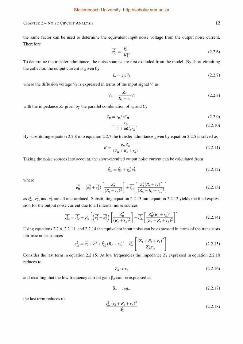
Rs*
Noiseless
2se
2ne
2ni
Figure 2.3: Equivalent noise sources connected to their associated noiseless BJT.
To express the noise voltage generated by the noise sources intrinsic to the BJT only, consider equation 2.2.22
with a source resistance Rs equal to zero, then
e2n = e2
x + i2nbr2x + i2nc
(rx + rπ)2
β2o
+ i2ncr2x
(ffT
)2
. (2.2.23)
Bearing in mind that rπ = βore, where re is the Shockley emitter resistance defined as the inverse of the trans-
conductance gm, equation 2.2.23 can be reduced to
e2n = e2
x + i2ncr2e + i2ncr2
x
(ffT
)2
(2.2.24)
since r2x (βore)
2.
Stellenbosch University http://scholar.sun.ac.za

CHAPTER 2 – NOISE CIRCUIT ANALYSIS 14
In order to find an expression for the noise current source, i2n shown in figure 2.3, consider the case where the
source resistance is infinite and that the equivalent input noise, e2ni, is produced solely by the product i2nR2
s . This
being the case, the input noise current can be solved by dividing each term in equation 2.2.22 by Rs and taking
the limit for Rs→ ∞ such that
i2n = i2nb + i2nc
(ffT
)2
. (2.2.25)
With the values of e2n and i2n defined, the transistor circuit can be represented by its noiseless equivalent as
depicted in figure 2.3. This representation, referred to as the chain representation when the transistor circuit is
defined by its transmission parameters, forms the basis for deriving the noise parameters of the circuit, discussed
in section 2.3.
2.2.2 Field Effect Transistors
The noise mechanisms of FETs are slightly more involved than those of BJTs. At first glance one would assume
that it would be sufficient to associate shot noise with the biasing drain current as is done with the base and
collector current for BJTs. However, as pointed out by Van der Ziel in [22], the noise generated within the
conduction channel of an FET can only be considered as thermal in nature. This first noise model for FETs
therefore only included a single thermal noise current source, dependent on the channel conductance of the
FET. Van der Ziel later revised this noise model when a sharp increase in gate noise was observed at higher
frequencies [23]. The increase in gate noise was attributed to the thermal noise generated in the conducting
channel which coupled capacitively between the conducting channel and the gate. This lead to the noise model
shown in figure 2.4, containing two partially correlated current noise sources, a gate and drain current source,
connected to the input and the output respectively.
gsg V m *
Gate Drain
* 2di
2gi
iR
gsC
gdC gdR
gsV +
- Gd
Source
Figure 2.4: Noise model for FETs proposed by Van der Ziel.
Stellenbosch University http://scholar.sun.ac.za
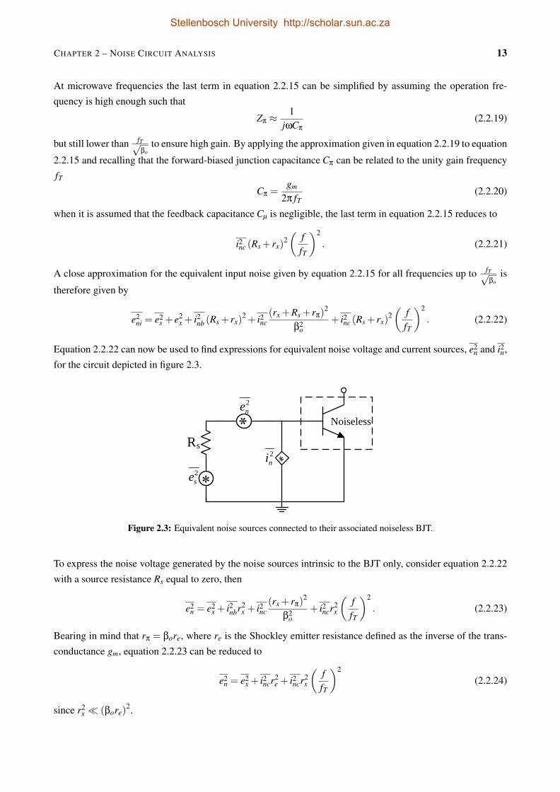
CHAPTER 2 – NOISE CIRCUIT ANALYSIS 15
The equivalent noise circuit developed by Van der Ziel proved to be adequate for early JFET and MOSFET de-
vices, and has widely been used as a basis for developing improved noise models for modern devices [24],
[25]. Modern FETs can be divided into three categories: Metal Oxide Semiconductor Field Effect Tran-
sistors (MOSFETs), Metal Semiconductor Field Effect Transistors (MESFETs), and High Electron Mobility
Transistors (HEMTs), the latter are often used in circuits operating at microwave frequencies due to their low
noise contribution. Although there are only small differences in the small signal models of the three types of
FETs, two distinct approaches have been developed in describing the noise mechanisms of these FETs - Phy-
sical models and Empirical models. The physical models are mostly based on the analytical solution of the
transport equations of charge carriers within the semiconductor lattice. While these models provide insight into
the physical origin of the various noise mechanisms found in FETs, they tend to require a number of theoretical
parameters that are not always readily available. Therefore nearly all physical noise models developed for FETs
incorporate proportionality constants in the definitions of the noise generators in order to fit the models more
accurately. Conversely, the empirical approach sets out to find what additional elements should be added to
the device small signal model to correctly model the noise contribution. Noise generators are placed in corres-
pondence to the available knowledge of the device’s noise mechanisms and using measured data, fitting factors
are extracted and applied to equations describing the generated noise. One such empirical model is the model
developed by Fukui [26] wherein a number of fitting factors are extracted from measurements in order to accu-
rately predict device noise performance. However, as described in [27], these fitting factors have no physical
meaning and may lead to nonphysical two-ports. In 1989 M.W. Pospieszalski published a two parameter noise
model for FETs [27] that is still widely used to model the noise of HEMTs in microwave circuits. It is this
model proposed by Pospieszalski that is discussed in this section. The noise model proposed by Pospieszalski
is shown in figure 2.5.
gsg V m *
Gate Drain
* 2dsi2
gsi gsR
gsCgsV +
-
Gd
Source
* 2gse
Figure 2.5: Noise model for FETs proposed by Pospiezalski.
The circuit shows a similar small signal model to the one used by Van der Ziel in figure 2.4, containing the follo-
wing small signal parameters: Gate-source resistance rgs, Gate-Source capacitance Cgs, Drain-Source conduc-
tance gds and neglects the Drain-Gate feedback resistance and capacitance. Included in Pospieszalski’s noise
model are three noise sources: Thermal gate noise voltage source e2gs, Thermal drain noise current source i2ds
and Gate leakage noise current source i2gs - although the gate leakage current source can be neglected for the
majority of HEMT noise models [28] and will therefore be omitted in the noise analysis to follow.
Stellenbosch University http://scholar.sun.ac.za
CHAPTER 2 – NOISE CIRCUIT ANALYSIS 16
The gate thermal noise voltage and drain thermal noise current, shown in figure 2.5, are defined by
egs2 = 4kTgrgs∆ f (2.2.26)
ids2= 4kTdgds∆ f (2.2.27)
where k is Boltzmann’s constant, and temperatures Tg and Td are the equivalent gate and drain temperatures,
respectively. In most cases the equivalent gate temperature Tg can be made equal to the device ambient tempera-
ture without introducing much error, thus enabling full noise characterisation by extracting only the equivalent
drain temperature from a single noise figure measurement. This process is discussed in section 2.4.2.
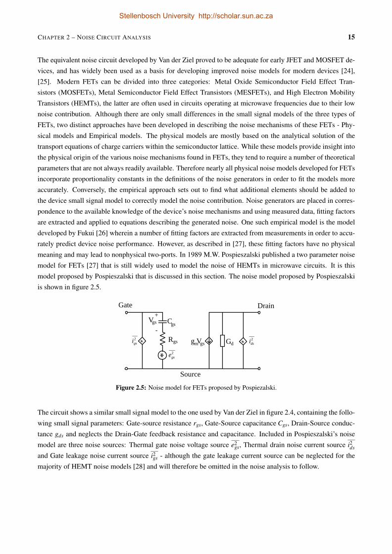
With the equivalent gate and drain temperatures as well as the small signal parameters known, the HEMT can
be represented as a noiseless admittance network with two external noise current sources applied to the input
and the output of the network as shown in figure 2.6.
I 1 I 2
+
V
-
1
+
V
-
221ni
22ni
Figure 2.6: Admittance representation of a noisy HEMT.
The spectral current density of the two noise sources i2n1 and i2n2 in the equivalent noise model of figure 2.6 can
be expressed in terms of equivalent noise conductances G1 and G2
in12= 4kT0G1 (2.2.28)
in22= 4kT0G2 (2.2.29)
and the correlation coefficient, describing the correlation between the two sources, by
ρc =in1i∗n2√i2n1i2n2
. (2.2.30)
By comparing the equivalent small signal noise model of figure 2.5 to the equivalent noiseless representation
of figure 2.6, expressions for the equivalent noise conductances and correlation between them can be obtained
in terms of the small signal parameters of the HEMT. That is,
G1 =Tg
T0
rgs(ωCgs)2
1+ω2C2gsr2
gs(2.2.31)
G2 =Tg
T0
g2mrgs
1+ω2C2gsr2
gs+
Td
T0gds (2.2.32)
and, by assuming the equivalent drain temperature Td = 0, the drain noise will be perfectly correlated with the
gate noise giving a correlation coefficient ρc =− j1.
Stellenbosch University http://scholar.sun.ac.za
CHAPTER 2 – NOISE CIRCUIT ANALYSIS 17
Therefore the correlation is defined by
in1i∗n2 = ρc
√i2n1i2n2 =− j
ωgmCgsrgs
1+ω2C2gsr2
gs
Tg
T0(2.2.33)
with the correlation coefficient being purely imaginary due to the capacitive coupling that exists between the
channel and the gate [29]. Having solved the noise currents i2n1 and i2n2 as well as the correlation between them
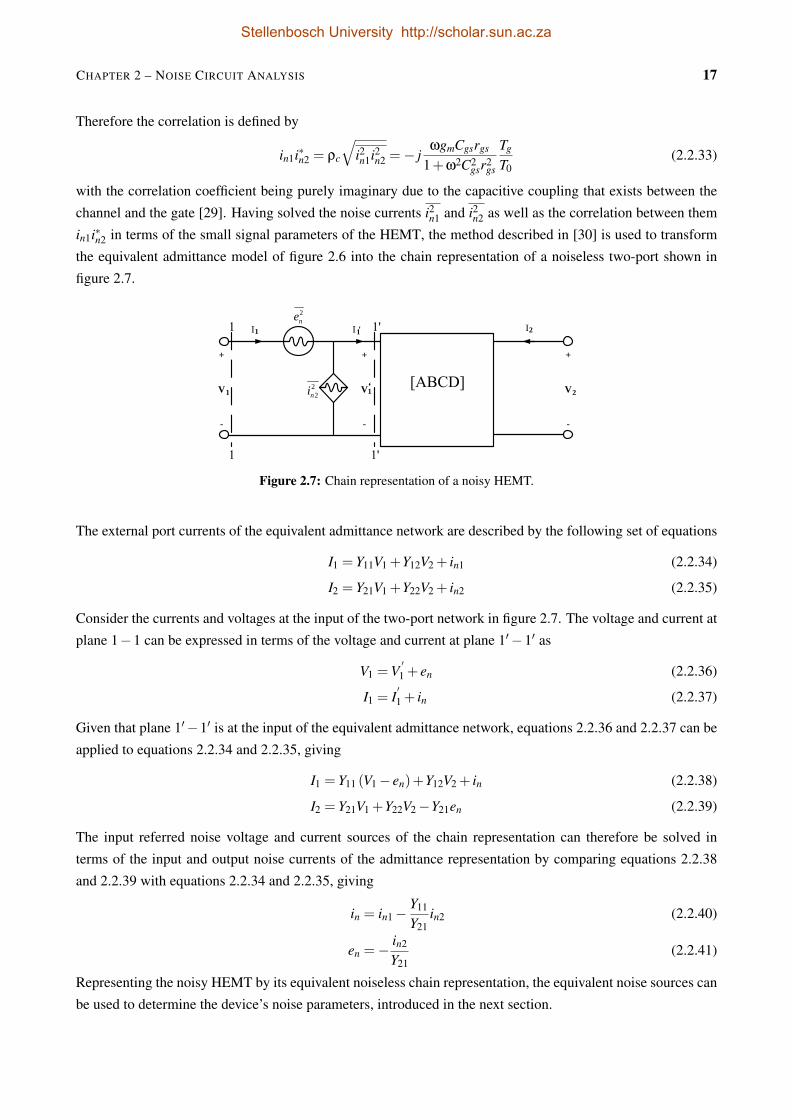
in1i∗n2 in terms of the small signal parameters of the HEMT, the method described in [30] is used to transform
the equivalent admittance model of figure 2.6 into the chain representation of a noiseless two-port shown in
figure 2.7.
+
V
-
1‘
+
V
-
2
+
V
-
1
I 2I 1 I ‘1
22ni
2ne
Figure 2.7: Chain representation of a noisy HEMT.
The external port currents of the equivalent admittance network are described by the following set of equations
I1 = Y11V1 +Y12V2 + in1 (2.2.34)
I2 = Y21V1 +Y22V2 + in2 (2.2.35)
Consider the currents and voltages at the input of the two-port network in figure 2.7. The voltage and current at
plane 1−1 can be expressed in terms of the voltage and current at plane 1′−1′ as
V1 =V′1 + en (2.2.36)
I1 = I′1 + in (2.2.37)
Given that plane 1′−1′ is at the input of the equivalent admittance network, equations 2.2.36 and 2.2.37 can be
applied to equations 2.2.34 and 2.2.35, giving
I1 = Y11 (V1− en)+Y12V2 + in (2.2.38)
I2 = Y21V1 +Y22V2−Y21en (2.2.39)
The input referred noise voltage and current sources of the chain representation can therefore be solved in
terms of the input and output noise currents of the admittance representation by comparing equations 2.2.38
and 2.2.39 with equations 2.2.34 and 2.2.35, giving
in = in1−Y11
Y21in2 (2.2.40)
en =−in2
Y21(2.2.41)
Representing the noisy HEMT by its equivalent noiseless chain representation, the equivalent noise sources can
be used to determine the device’s noise parameters, introduced in the next section.
Stellenbosch University http://scholar.sun.ac.za
CHAPTER 2 – NOISE CIRCUIT ANALYSIS 18
2.3 Noise Parameters
In section 2.2 techniques are discussed whereby the noise generated within BJTs and FETs can be represented as
equivalent noise sources applied to the input of the respective devices. In this section another set of parameters
used to characterise the noise performance of linear two-ports are introduced. These parameters are referred to
as noise parameters.
2.3.1 Equivalent two-port Noise Parameters
The first of the noise parameters is the equivalent noise resistance. It follows from the definition of thermal
noise described in section 2.1.2 that the mean square fluctuations produced at the terminals of an open circuit
resistor of value R at a temperature T is given by
e2 = 4kT R∆ f . (2.3.1)
The equivalent noise resistance, Rn, of a network that produces a noise voltage e2 is therefore defined by
Rn =e2
kT0∆ f(2.3.2)
where T0 is the standard temperature, 290K. It should be noted that the quantity Rn does not represent a physical
resistance within the network but is merely used as a means to compare the noise generated by the internal noise
sources of the network to the noise generated by the physical resistors of the network [31].
The second noise parameter is the noise factor (F) also referred to as noise figure (NF), where the noise figure
is related to the noise factor by
NF = 10log(F) (2.3.3)
As defined by Friis [32], this is a measure of degradation in the signal to noise ratio (S/N) that occurs when a
signal passes through the two-port network
F =Si/Ni
So/No(2.3.4)
where i denotes the input port and o denotes the output port of the two-port network. According to IEEE
standards, the expression for the noise factor of a linear two-port given in equation 2.3.4 is also defined as the
ratio of the total output noise power per unit bandwidth to the portion of the output noise power produced by
the source at standard temperature T0 = 290K [33], that is
F =Total out put Noise per unit bandwidth
Portion o f out put Noise produced by the source. (2.3.5)
For an arbitrary source impedance Ni is given by
Ni = kT ∆ f (2.3.6)
as defined by Nyquist. Furthermore the gain of the linear two-port is expressed as the ratio of the output signal
to the input signal, that is
G =So
Si. (2.3.7)
Stellenbosch University http://scholar.sun.ac.za
CHAPTER 2 – NOISE CIRCUIT ANALYSIS 19
Substituting equations 2.3.7 and 2.3.6 into equation 2.3.4 the noise factor can be expressed as
F =
(1G
)(No
kT ∆ f
). (2.3.8)
Seeing that the gain, expressed in equation 2.3.7, is independent of the output circuit connected to the two-
port network, the output network has no effect on the noise figure of two-port network. However, since the
available power from the signal source, Si, is dependent on the degree of mismatch between the two-port
network and the source, the output noise power, No, and therefore also the noise figure depend on the source
impedance presented to the two-port network. Due to the fact that the noise figure varies with the degree of
mismatch between the source and the two-port network, there exists an optimum source admittance Yopt =
Gopt + jBopt for which the noise factor of the linear two-port is a minimum, referred to as Fmin. Knowing these
four parameters: Rn, Fmin, Gopt , and Bopt the noise figure of any linear two-port network in any input termination
can be determined using
F = Fmin +RN
GS|YS−Yopt |2 (2.3.9)
where YS = GS + jBS is the source admittance presented to the network.
Stellenbosch University http://scholar.sun.ac.za
CHAPTER 2 – NOISE CIRCUIT ANALYSIS 20
2.3.2 Noise Parameters of a Bipolar Junction Transistor
2.3.2.1 Motchenbacher’s Noise Model
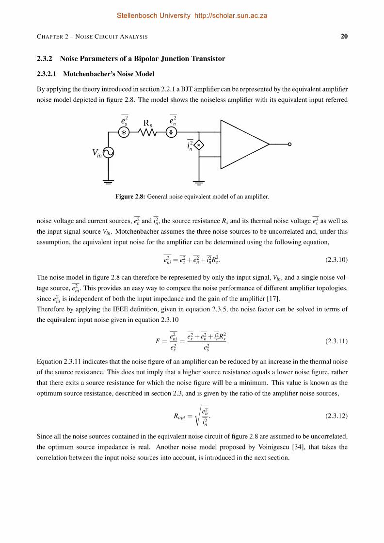
By applying the theory introduced in section 2.2.1 a BJT amplifier can be represented by the equivalent amplifier
noise model depicted in figure 2.8. The model shows the noiseless amplifier with its equivalent input referred
**
Rs
in
*
V2ni
2se 2
ne
Figure 2.8: General noise equivalent model of an amplifier.
noise voltage and current sources, e2n and i2n, the source resistance Rs and its thermal noise voltage e2
s as well as
the input signal source Vin. Motchenbacher assumes the three noise sources to be uncorrelated and, under this
assumption, the equivalent input noise for the amplifier can be determined using the following equation,
e2ni = e2
s + e2n + i2nR2
s . (2.3.10)
The noise model in figure 2.8 can therefore be represented by only the input signal, Vin, and a single noise vol-
tage source, e2ni. This provides an easy way to compare the noise performance of different amplifier topologies,
since e2ni is independent of both the input impedance and the gain of the amplifier [17].
Therefore by applying the IEEE definition, given in equation 2.3.5, the noise factor can be solved in terms of
the equivalent input noise given in equation 2.3.10
F =e2
ni
e2s
=e2
s + e2n + i2nR2
s
e2s
. (2.3.11)
Equation 2.3.11 indicates that the noise figure of an amplifier can be reduced by an increase in the thermal noise
of the source resistance. This does not imply that a higher source resistance equals a lower noise figure, rather
that there exits a source resistance for which the noise figure will be a minimum. This value is known as the
optimum source resistance, described in section 2.3, and is given by the ratio of the amplifier noise sources,
Ropt =
√e2
n
i2n. (2.3.12)
Since all the noise sources contained in the equivalent noise circuit of figure 2.8 are assumed to be uncorrelated,
the optimum source impedance is real. Another noise model proposed by Voinigescu [34], that takes the
correlation between the input noise sources into account, is introduced in the next section.
Stellenbosch University http://scholar.sun.ac.za
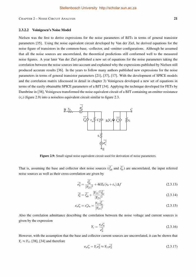
CHAPTER 2 – NOISE CIRCUIT ANALYSIS 21
2.3.2.2 Voinigescu’s Noise Model
Nielsen was the first to derive expressions for the noise parameters of BJTs in terms of general transistor
parameters [35]. Using the noise equivalent circuit developed by Van der Ziel, he derived equations for the
noise figure of transistors in the common-base, -collector, and -emitter configurations. Although he assumed
that all the noise sources are uncorrelated, the theoretical predictions still conformed well to the measured
noise figures. A year later Van der Ziel published a new set of equations for the noise parameters taking the
correlation between the noise sources into account and explained why the expressions published by Nielsen still
produced accurate results [36]. In the years to follow many authors published new expressions for the noise
parameters in terms of general transistor parameters [21], [37], [17]. With the development of SPICE models
and the correlation matrix (discussed in detail in chapter 3) Voinigescu developed a new set of equations in
terms of the easily obtainable SPICE parameters of a BJT [34]. Applying the technique developed for FETs by
Dambrine in [38], Voinigescu transformed the noise equivalent circuit of a BJT containing an emitter resistance
(re) (figure 2.9) into a noiseless equivalent circuit similar to figure 2.3.
rb
πg V m*rπ πC
B C
*
*
E
*
ro
re
2nci
2be
2nbi
2ee
Figure 2.9: Small signal noise equivalent circuit used for derivation of noise parameters.
That is, assuming the base and collector shot noise sources (i2nb and i2nc) are uncorrelated, the input referred
noise sources as well as their cross-correlation are given by
e2n =
i2nc
|Y21|2+4kT0 (rb + re)∆ f (2.3.13)
i2n = i2nb +|Y11|2i2nc
|Y21|2(2.3.14)
eni∗n = e∗nin =Y11i2nc
|Y21|2(2.3.15)
Also the correlation admittance describing the correlation between the noise voltage and current sources is
given by the expression
Yc =eni∗ne2
n
(2.3.16)
However, with the assumption that the base and collector current sources are uncorrelated, it can be shown that
Yc ≈ Y11 [38], [34] and therefore
eni∗n = Yce2n ≈ Y11e2
n (2.3.17)
Stellenbosch University http://scholar.sun.ac.za
CHAPTER 2 – NOISE CIRCUIT ANALYSIS 22
Voinigescu uses the correlation matrix to derive expressions for the noise parameters as shown below. The
noise parameters can be expressed in terms of the elements of the chain representation of the correlation matrix
(refer to chapter 3 for the derivation)
Rn =Cee∗
2kT0(2.3.18)
Yopt =
√Cii∗
Cee∗−[
ℑ
(Cei∗
Cee∗
)]2
+ jℑ(
Cei∗
Cee∗
)(2.3.19)
Fmin = 1+Cei∗+Cee∗Yopt
kT0(2.3.20)
where the elements of the correlation matrix are defined as the auto- and cross-correlated spectral power densi-
ties of the intrinsic noise sources of the BJT. That is,
Cene∗n2kT0∆ f
=e2
n
4kT0∆ f=
i2nc
4kT0∆ f |Y21|2+(rb + re) (2.3.21)
Ceni∗n2kT0∆ f
=e∗nin
4kT0∆ f≈ Y11i2nc
4kT0∆ f |Y21|2(2.3.22)
Cini∗n2kT0∆ f
=i2n
4kT0∆ f=
i2nb4kT0∆ f
+|Y11|2i2nc
4kT0∆ f |Y21|2(2.3.23)
By neglecting feedback parameters rµ and Cµ as well as the Early effect, it is found that |Y21| is approximately
equal to the transconductance gm. Since the collector current, expressed in terms of reverse saturation current
Is and base-emitter voltage vBE can be approximated as in equation 2.3.25
iC = IS
(e
vBEnVT −1
)(2.3.24)
≈ IS
(e
vBEnVT
)(2.3.25)
where n is the collector current ideality factor, usually assumed 1, and VT is the thermal voltage given by
VT =kT0
q(2.3.26)
It therefore follows that
|Y21|= gm =∂iC
∂vBE|Q−point (2.3.27)
=IC
nVT(2.3.28)
Substituting equations 2.3.21 to 2.3.23 into equations 2.3.18 to 2.3.20 the noise parameters of a BJT can be
expressed in terms of the transistor parameters, using the relationships shown in equations 2.3.28 and 2.2.20.
Hence,
Rn =n2VT
2IC+ rE + rB (2.3.29)
Yopt =f
fT Rn(
√IC
2VT(rE + rB)(1+
f 2T
βo f 2 )+n2 f 2
T4βo f 2 − j
n2) (2.3.30)
Fmin = 1+nβo
+ffT
√2ICVT
(rE + rB)(1+f 2T
βo f 2 )+n2 f 2
Tβo f 2 (2.3.31)
Stellenbosch University http://scholar.sun.ac.za
CHAPTER 2 – NOISE CIRCUIT ANALYSIS 23
These expressions make it possible to characterise the noise performance of a BJT using only the small signal
parameters of the device. Furthermore, the values of the equivalent noise voltage and current sources in figure
2.3, as well as the correlation between them, can be solved from these equations using the theory on the
correlation matrix, described in chapter 3.
2.3.3 Noise Parameters of Field Effect Transistors
In section 2.2.2 an equivalent noise model for HEMTs is derived in the form of a noiseless two-port network -
defined by the transmission parameters of the small signal model of an HEMT - with a correlated noise voltage
source and noise current source connected to the input of the two-port. This equivalent noise representation,
shown in figure 2.7, is used in this section to derive the noise parameters of an HEMT in terms of the device’s
small signal parameters. The spectral densities of the equivalent noise voltage and current sources are given by
e2n = 4kT0Rn (2.3.32)
i2n = 4kT0gn (2.3.33)
where Rn and gn are referred to as the equivalent noise resistance and noise conductance, respectively. Further-
more the correlation between the two sources are defined by the correlation admittance
Zc = Rc + jXc (2.3.34)
Similar to the method applied by Voinigescu in section 2.3.2.2, the correlation admittance is defined by assu-
ming no correlation between the equivalent gate and drain noise sources egs and ids. That is, in terms of the
small signal parameters,
Zc ≈ Z11 = rsg +1
jωCsg(2.3.35)
The equivalent noise resistance and conductance can be solved in terms of the small signal parameters of the
HEMT by substituting the equivalent noise conductance values, derived in equations 2.2.31 and 2.2.32, into the
expressions for the noise voltage and current sources shown in equations 2.2.40 and 2.2.41, giving
Rn =G2
|Y21|2(2.3.36)
gn = G1−G2|Y11|2
|Y21|2(2.3.37)
or in terms of the small signal parameters
Rn =Tg
T0rgs +
Td
T0
gds
g2m
(1+ω
2C2gsr
2gs)
(2.3.38)
gn =
(ffT
)2 gdsTd
T0(2.3.39)
given that
fT =gm
2πCgs(2.3.40)
Stellenbosch University http://scholar.sun.ac.za

CHAPTER 2 – NOISE CIRCUIT ANALYSIS 24
By performing an analysis analogous to that of section 3.2 Pucel et al. derived expression for the noise parame-
ters in terms of the noise resistance, conductance and correlation impedance [24], with the real and imaginary
parts of the optimum source impedance being equal to
Ropt =
√R2
c +Rn
gn(2.3.41)
Xopt =−Xc (2.3.42)
and the minimum noise figure expressed as
Fmin = 1+2gn (Rc +Ropt) (2.3.43)
Substituting equations 2.3.35, 2.3.38 and 2.3.39 into equations 2.3.41 to 2.3.43, the noise parameters are solved
in terms of the HEMT small signal parameters and equivalent gate and drain temperatures
Ropt =
√(fT
f
)2 rgs
gdsTg
Td+ r2
gs (2.3.44)
Xopt =1
ωCgs(2.3.45)
Tmin = 2ffT
√gdsrgsTgTd +
(ffT
)2
r2gsg
2dsT
2d +2
(ffT
)2
rgsgdsTd (2.3.46)
where the minimum noise temperature (Tmin) is related to the minimum noise factor by
Tmin = (Fmin−1)T0 (2.3.47)
Furthermore, under the condition thatffT
√Tg
Td
1rgsgds
(2.3.48)
then
Ropt rgs (2.3.49)
and equations 2.3.44 and 2.3.46 reduce to
Ropt =fT
f
√rgs
gdsTg
Td(2.3.50)
Tmin = 2ffT
√gdsrgsTgTd (2.3.51)
Stellenbosch University http://scholar.sun.ac.za
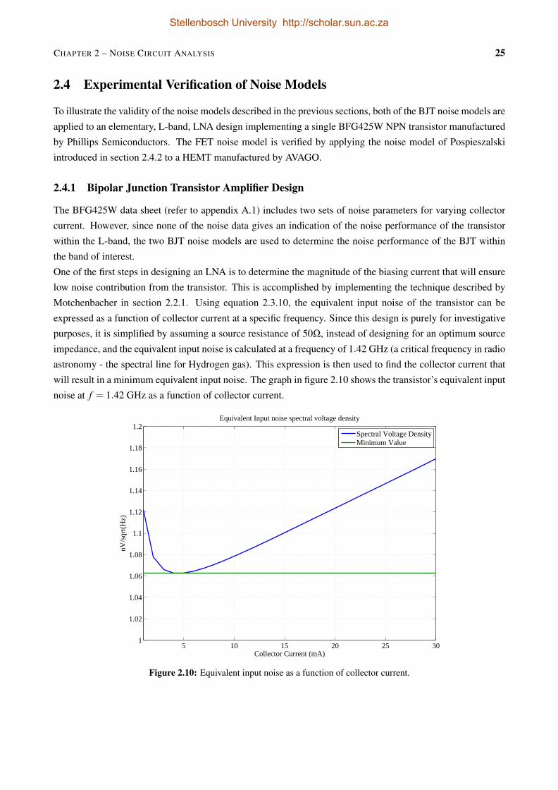
CHAPTER 2 – NOISE CIRCUIT ANALYSIS 25
2.4 Experimental Verification of Noise Models
To illustrate the validity of the noise models described in the previous sections, both of the BJT noise models are
applied to an elementary, L-band, LNA design implementing a single BFG425W NPN transistor manufactured
by Phillips Semiconductors. The FET noise model is verified by applying the noise model of Pospieszalski
introduced in section 2.4.2 to a HEMT manufactured by AVAGO.
2.4.1 Bipolar Junction Transistor Amplifier Design
The BFG425W data sheet (refer to appendix A.1) includes two sets of noise parameters for varying collector
current. However, since none of the noise data gives an indication of the noise performance of the transistor
within the L-band, the two BJT noise models are used to determine the noise performance of the BJT within
the band of interest.
One of the first steps in designing an LNA is to determine the magnitude of the biasing current that will ensure
low noise contribution from the transistor. This is accomplished by implementing the technique described by
Motchenbacher in section 2.2.1. Using equation 2.3.10, the equivalent input noise of the transistor can be
expressed as a function of collector current at a specific frequency. Since this design is purely for investigative
purposes, it is simplified by assuming a source resistance of 50Ω, instead of designing for an optimum source
impedance, and the equivalent input noise is calculated at a frequency of 1.42 GHz (a critical frequency in radio
astronomy - the spectral line for Hydrogen gas). This expression is then used to find the collector current that
will result in a minimum equivalent input noise. The graph in figure 2.10 shows the transistor’s equivalent input
noise at f = 1.42 GHz as a function of collector current.
5 10 15 20 25 301
1.02
1.04
1.06
1.08
1.1
1.12
1.14
1.16
1.18
1.2
Collector Current (mA)
nV/s
qrt(H
z)
Equivalent Input noise spectral voltage density
Spectral Voltage DensityMinimum Value
Figure 2.10: Equivalent input noise as a function of collector current.
Stellenbosch University http://scholar.sun.ac.za

CHAPTER 2 – NOISE CIRCUIT ANALYSIS 26
It is clear from figure 2.10 that there is an ideal value for the collector current for which the equivalent input
noise contributed by the transistor is a minimum. The biasing circuit of the LNA is therefore designed such that
the collector current equals this optimum value.
2.4.1.1 Motchenbacher’s noise model
With the optimum collector current for low noise contribution known, the transistor can be represented as a
noiseless transistor with two equivalent noise sources applied to the input as depicted in figure 2.3. The values
of the equivalent noise voltage and current sources (en and in) are solved, for the desired collector current, using
equations 2.2.24 and 2.2.25 respectively. To investigate the accuracy of this model the LNA circuit is simulated
in RF/Microwave simulation software, Microwave Office (MWO), developed by AWR. Consider the circuit
schematic of the LNA shown in figure 2.11.
ACVSID=V1Mag=1 VAng=0 DegOffset=0 VDCVal=0 V
CAPID=C1C=1e-8 F
CAPID=C2C=1e-8 F
DCVSID=V2V=9 V
C
B
E
1
2
3
GBJT3ID=GP1
T
1
2
RESTID=IN1R=130000 OhmT=17 DegC
T
1
2
RESTID=IN3R=1300 OhmT=17 DegC
T12
RESTID=IN4R=50 OhmT=17 DegC
T
1
2
RESTID=IN5R=50 OhmT=17 DegC
V_NSMTRID=VNS1InpSrc=V1
Figure 2.11: SPICE simulation of LNA circuit biased for minimum noise contribution.
The SPICE parameters of the BFG425W transistor is entered into the transistor model provided by MWO and
the noise voltage at the output of the LNA is simulated using the linear simulator in MWO. By disabling the
internal noise model of the transistor element, the LNA circuit can be simulated using the noiseless equivalent
circuit of Motchenbacher. The LNA circuit containing a noiseless transistor with the two equivalent noise
sources applied to the input is shown in figure 2.12. Figure 2.13 shows a graph comparing the simulated output
noise voltage of the two circuits depicted in figures 2.11 and 2.12. It is clear that the simulation results from the
noise model proposed by Motchenbacher deviates slightly from the internal noise model of MWO, which is to
be expected since the equivalent input noise sources are assumed to be uncorrelated.
Stellenbosch University http://scholar.sun.ac.za
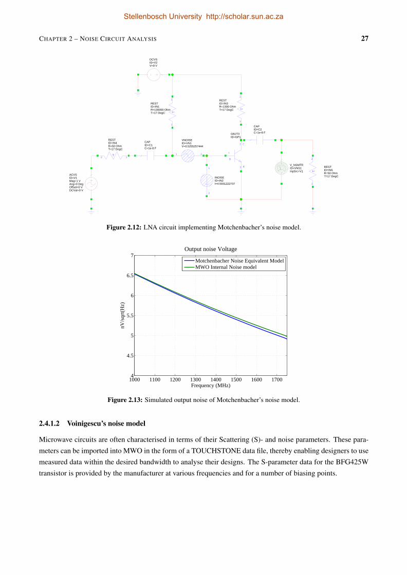
CHAPTER 2 – NOISE CIRCUIT ANALYSIS 27
CAPID=C1C=1e-8 F
CAPID=C2C=1e-8 F
DCVSID=V2V=9 V
C
B
E
1
2
3
GBJT3ID=GP1
T
1
2
RESTID=IN1R=130000 OhmT=17 DegC
T
1
2
RESTID=IN3R=1300 OhmT=17 DegC
1 2
VNOISEID=VN1V=0.5255257444
1
2
INOISEID=IN2I=4.5931222737
V_NSMTRID=VNS1InpSrc=V1
ACVSID=V1Mag=1 VAng=0 DegOffset=0 VDCVal=0 V
T12
RESTID=IN4R=50 OhmT=17 DegC
T
1
2
RESTID=IN5R=50 OhmT=17 DegC
Figure 2.12: LNA circuit implementing Motchenbacher’s noise model.
1000 1100 1200 1300 1400 1500 1600 17004
4.5
5
5.5
6
6.5
7Output noise Voltage
Frequency (MHz)
nV/s
qrt(H
z)
Motchenbacher Noise Equivalent ModelMWO Internal Noise model
Figure 2.13: Simulated output noise of Motchenbacher’s noise model.
2.4.1.2 Voinigescu’s noise model
Microwave circuits are often characterised in terms of their Scattering (S)- and noise parameters. These para-
meters can be imported into MWO in the form of a TOUCHSTONE data file, thereby enabling designers to use
measured data within the desired bandwidth to analyse their designs. The S-parameter data for the BFG425W
transistor is provided by the manufacturer at various frequencies and for a number of biasing points.
Stellenbosch University http://scholar.sun.ac.za
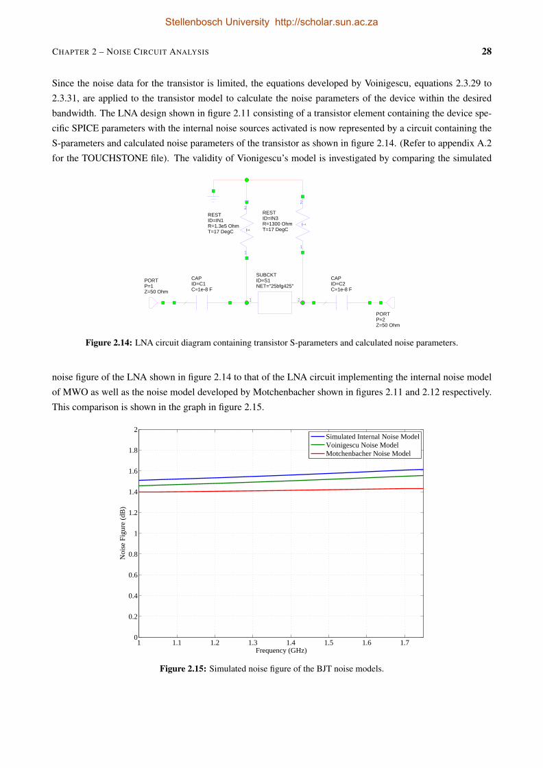
CHAPTER 2 – NOISE CIRCUIT ANALYSIS 28
Since the noise data for the transistor is limited, the equations developed by Voinigescu, equations 2.3.29 to
2.3.31, are applied to the transistor model to calculate the noise parameters of the device within the desired
bandwidth. The LNA design shown in figure 2.11 consisting of a transistor element containing the device spe-
cific SPICE parameters with the internal noise sources activated is now represented by a circuit containing the
S-parameters and calculated noise parameters of the transistor as shown in figure 2.14. (Refer to appendix A.2
for the TOUCHSTONE file). The validity of Vionigescu’s model is investigated by comparing the simulated
CAPID=C1C=1e-8 F
CAPID=C2C=1e-8 F
T
1
2
RESTID=IN3R=1300 OhmT=17 DegCT
1
2
RESTID=IN1R=1.3e5 OhmT=17 DegC
1 2
SUBCKTID=S1NET="25bfg425"
PORTP=1Z=50 Ohm
PORTP=2Z=50 Ohm
Figure 2.14: LNA circuit diagram containing transistor S-parameters and calculated noise parameters.
noise figure of the LNA shown in figure 2.14 to that of the LNA circuit implementing the internal noise model
of MWO as well as the noise model developed by Motchenbacher shown in figures 2.11 and 2.12 respectively.
This comparison is shown in the graph in figure 2.15.
1 1.1 1.2 1.3 1.4 1.5 1.6 1.70
0.2
0.4
0.6
0.8
1
1.2
1.4
1.6
1.8
2
Frequency (GHz)
Noi
se F
igur
e (d
B)
Simulated Internal Noise ModelVoinigescu Noise ModelMotchenbacher Noise Model
Figure 2.15: Simulated noise figure of the BJT noise models.
Stellenbosch University http://scholar.sun.ac.za
CHAPTER 2 – NOISE CIRCUIT ANALYSIS 29
The graph in figure 2.15 shows that both the models of Voinigescu and Motchenbacher prove to be adequate
for predicting the noise performance of a BJT. By considering the deviation of noise figure calculated from
Motchenbacher’s model, the importance of including the correlation between the input noise sources is empha-
sized.
2.4.2 Field Effect Transistors - Pospieszalski’s Noise Model
This section uses the noise model of Pospieszalski described in section 2.2.2 to determine the minimum noise
figure of a GaAs HEMT manufactured by AVAGO - VMMK1218. (Refer to appendix B for the device noise
and small signal parameters). The aim of this investigation is to determine the equivalent gate and drain noise
temperatures (Tg and Td) from the measured noise parameters provided, and then to use these values to predict
the noise performance of the HEMT based on the expressions derived by Pospieszalski. Consider the noise
parameters, for VDS = 3V and IDS = 20mA, measured at a frequency of 10GHz. Since the optimum source
resistance (Ropt) is significantly larger than the value of the gate source resistance (rgs), the reduced equations
for the source resistance and minimum noise temperature (equations 2.3.50 and 2.3.51) are used to determine
the values of drain and gate noise constants, defined by
Kd = Tdgds (2.4.1)
Kg = Tgrgs (2.4.2)
respectively. Thus, by solving Kd and Kg from
Ropt =ffT
√Kg
Kd(2.4.3)
Tmin = 2ffT
√KdKg (2.4.4)
where fT is given by equation 2.3.40, the equivalent drain and gate noise temperatures are calculated using
equations 2.4.1 and 2.4.2, respectively. Since the noise generated by the HEMT is considered to be frequency
independent, these values of the equivalent noise temperatures, together with the small signal parameters of the
HEMT, are used in equation 2.3.46 to calculate the equivalent noise temperature within a desired bandwidth.
Figure 2.16 shows a graph comparing the measured minimum noise figure provided by the manufacturer, over
a bandwidth from 2-18 GHz, with the minimum noise figure calculated using the above mentioned method.
Stellenbosch University http://scholar.sun.ac.za
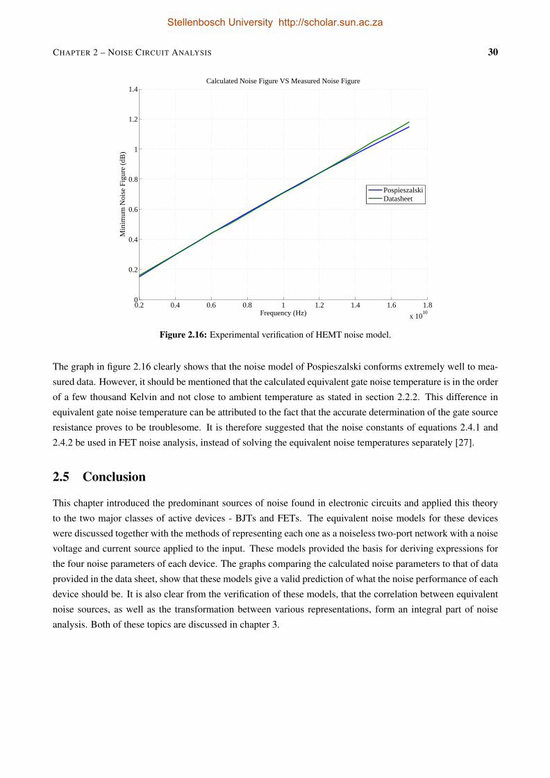
CHAPTER 2 – NOISE CIRCUIT ANALYSIS 30
0.2 0.4 0.6 0.8 1 1.2 1.4 1.6 1.8x 10¹⁰
0
0.2
0.4
0.6
0.8
1
1.2
1.4Calculated Noise Figure VS Measured Noise Figure
Min
imum
Noi
se F
igur
e (d
B)
Frequency (Hz)
PospieszalskiDatasheet
Figure 2.16: Experimental verification of HEMT noise model.
The graph in figure 2.16 clearly shows that the noise model of Pospieszalski conforms extremely well to mea-
sured data. However, it should be mentioned that the calculated equivalent gate noise temperature is in the order
of a few thousand Kelvin and not close to ambient temperature as stated in section 2.2.2. This difference in
equivalent gate noise temperature can be attributed to the fact that the accurate determination of the gate source
resistance proves to be troublesome. It is therefore suggested that the noise constants of equations 2.4.1 and
2.4.2 be used in FET noise analysis, instead of solving the equivalent noise temperatures separately [27].
2.5 Conclusion
This chapter introduced the predominant sources of noise found in electronic circuits and applied this theory
to the two major classes of active devices - BJTs and FETs. The equivalent noise models for these devices
were discussed together with the methods of representing each one as a noiseless two-port network with a noise
voltage and current source applied to the input. These models provided the basis for deriving expressions for
the four noise parameters of each device. The graphs comparing the calculated noise parameters to that of data
provided in the data sheet, show that these models give a valid prediction of what the noise performance of each
device should be. It is also clear from the verification of these models, that the correlation between equivalent
noise sources, as well as the transformation between various representations, form an integral part of noise
analysis. Both of these topics are discussed in chapter 3.
Stellenbosch University http://scholar.sun.ac.za
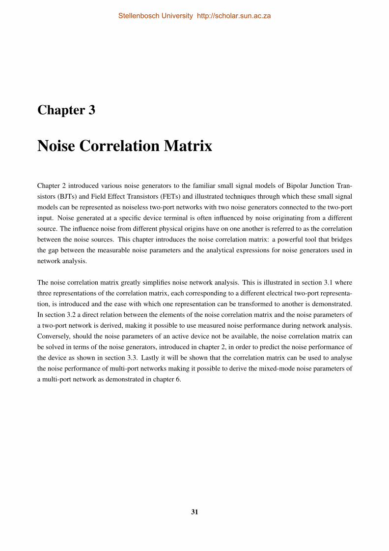
Chapter 3
Noise Correlation Matrix
Chapter 2 introduced various noise generators to the familiar small signal models of Bipolar Junction Tran-
sistors (BJTs) and Field Effect Transistors (FETs) and illustrated techniques through which these small signal
models can be represented as noiseless two-port networks with two noise generators connected to the two-port
input. Noise generated at a specific device terminal is often influenced by noise originating from a different
source. The influence noise from different physical origins have on one another is referred to as the correlation
between the noise sources. This chapter introduces the noise correlation matrix: a powerful tool that bridges
the gap between the measurable noise parameters and the analytical expressions for noise generators used in
network analysis.
The noise correlation matrix greatly simplifies noise network analysis. This is illustrated in section 3.1 where
three representations of the correlation matrix, each corresponding to a different electrical two-port representa-
tion, is introduced and the ease with which one representation can be transformed to another is demonstrated.
In section 3.2 a direct relation between the elements of the noise correlation matrix and the noise parameters of
a two-port network is derived, making it possible to use measured noise performance during network analysis.
Conversely, should the noise parameters of an active device not be available, the noise correlation matrix can
be solved in terms of the noise generators, introduced in chapter 2, in order to predict the noise performance of
the device as shown in section 3.3. Lastly it will be shown that the correlation matrix can be used to analyse
the noise performance of multi-port networks making it possible to derive the mixed-mode noise parameters of
a multi-port network as demonstrated in chapter 6.
31
Stellenbosch University http://scholar.sun.ac.za
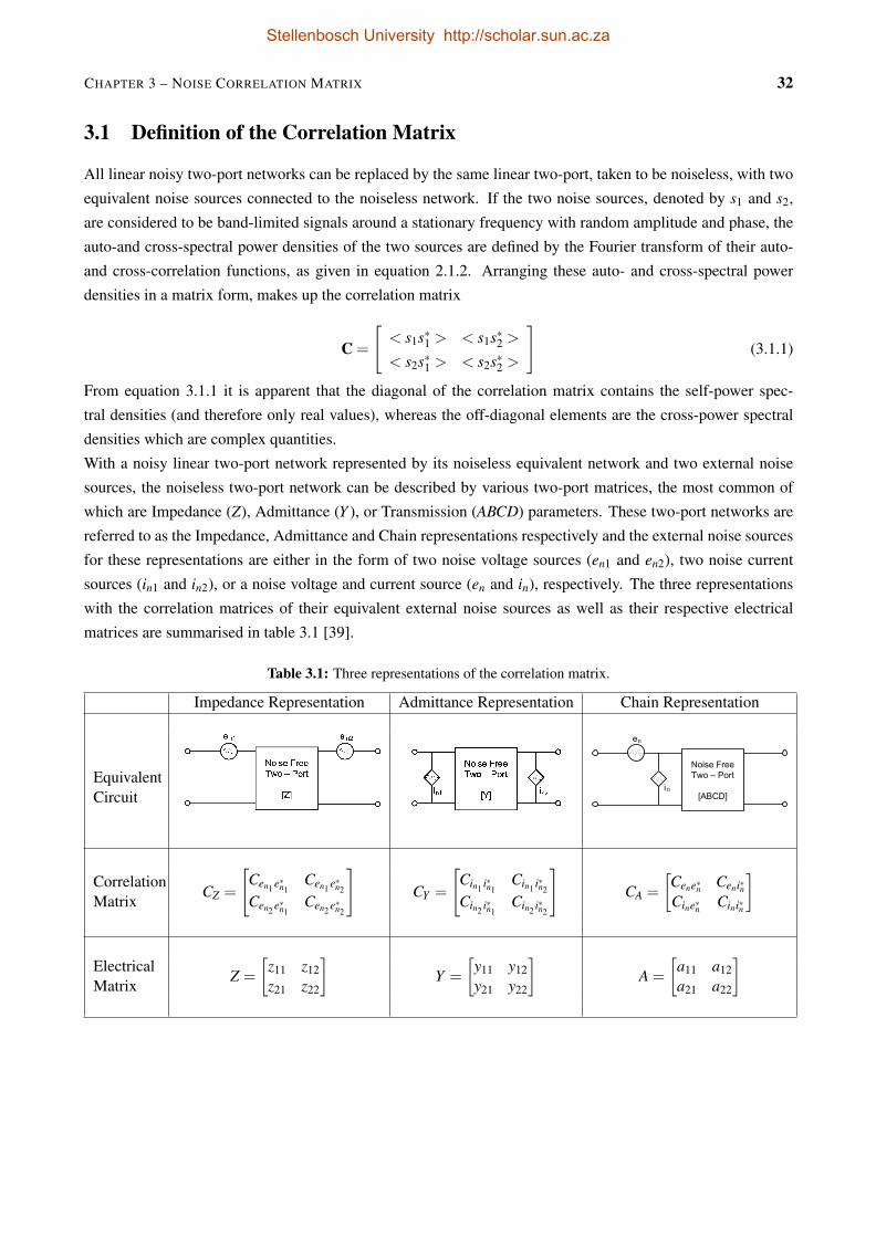
CHAPTER 3 – NOISE CORRELATION MATRIX 32
3.1 Definition of the Correlation Matrix
All linear noisy two-port networks can be replaced by the same linear two-port, taken to be noiseless, with two
equivalent noise sources connected to the noiseless network. If the two noise sources, denoted by s1 and s2,
are considered to be band-limited signals around a stationary frequency with random amplitude and phase, the
auto-and cross-spectral power densities of the two sources are defined by the Fourier transform of their auto-
and cross-correlation functions, as given in equation 2.1.2. Arranging these auto- and cross-spectral power
densities in a matrix form, makes up the correlation matrix
C =
[< s1s∗1 > < s1s∗2 >
< s2s∗1 > < s2s∗2 >
](3.1.1)
From equation 3.1.1 it is apparent that the diagonal of the correlation matrix contains the self-power spec-
tral densities (and therefore only real values), whereas the off-diagonal elements are the cross-power spectral
densities which are complex quantities.
With a noisy linear two-port network represented by its noiseless equivalent network and two external noise
sources, the noiseless two-port network can be described by various two-port matrices, the most common of
which are Impedance (Z), Admittance (Y ), or Transmission (ABCD) parameters. These two-port networks are
referred to as the Impedance, Admittance and Chain representations respectively and the external noise sources
for these representations are either in the form of two noise voltage sources (en1 and en2), two noise current
sources (in1 and in2), or a noise voltage and current source (en and in), respectively. The three representations
with the correlation matrices of their equivalent external noise sources as well as their respective electrical
matrices are summarised in table 3.1 [39].
Table 3.1: Three representations of the correlation matrix.
Impedance Representation Admittance Representation Chain Representation
EquivalentCircuit
n
n
CorrelationMatrix
CZ =
[Cen1 e∗n1
Cen1 e∗n2
Cen2 e∗n1Cen2 e∗n2
]CY =
[Cin1 i∗n1
Cin1 i∗n2
Cin2 i∗n1Cin2 i∗n2
]CA =
[Cene∗n Ceni∗nCine∗n Cini∗n
]
ElectricalMatrix
Z =
[z11 z12z21 z22
]Y =
[y11 y12y21 y22
]A =
[a11 a12a21 a22
]
Stellenbosch University http://scholar.sun.ac.za
CHAPTER 3 – NOISE CORRELATION MATRIX 33
Since the two-port networks, shown in table 3.1, are defined by noiseless electrical matrices, transforming
the electrical matrices from one representation to another can easily be done by applying the correct set of
equations summarized in [15]. Hillbrand and Russer showed that one of the most useful properties of the cor-
relation matrix is the ability to transform between equivalent noise representations, by using extremely simple
transformation matrices. Table 3.2 shows a summary of the transformation matrices, T, used to transform the
noise sources between representations. To transform correlation matrix C1 to a different representation C2, the
appropriate transformation matrix, T is used as follows,
C2 = TC1T† (3.1.2)
where the dagger (†) denotes the Hermitian matrix or conjugate-transpose of transformation matrix T. The
mean square value of the noise sources of the final representation can then be solved from the transformed
correlation matrix using the relation given in equation 2.1.3. Conversely, given that the noise generators within
a passive network are all thermal in nature, the impedance and admittance representations of the correlation
matrix can readily be solved from the impedance or admittance electrical matrices. That is, for a passive
network,
CZ = kT [Z+Z∗] (3.1.3)
CY = kT [Y+Y∗] (3.1.4)
Table 3.2: Transformation matrices for the three correlation matrix representations.
Resulting ReresentationOriginal Representation
Admittance Impedance Chain
Admittance[
1 00 1
] [y11 y12y21 y22
] [−y11 1−y21 0
]
Impedance[
z11 z12z21 z22
] [1 00 1
] [1 −z110 −z21
]
Chain[
0 a121 a22
] [1 −a110 −a21
] [1 00 1
]
Two-port networks can often be simplified by describing them as an interconnection of a number of two-ports in
either series, parallel or cascade. The correlation matrix can be used to express the resulting noise generated by
the composite two-port network. That is, using the appropriate representation, the resulting correlation matrix
is related to the original matrices by
CZ = CZ1 +CZ2 (Series) (3.1.5)
CY = CY 1 +CY 2 (Parallel) (3.1.6)
CA = A1CA2A†1 +CA1 (Cascade) (3.1.7)
Stellenbosch University http://scholar.sun.ac.za
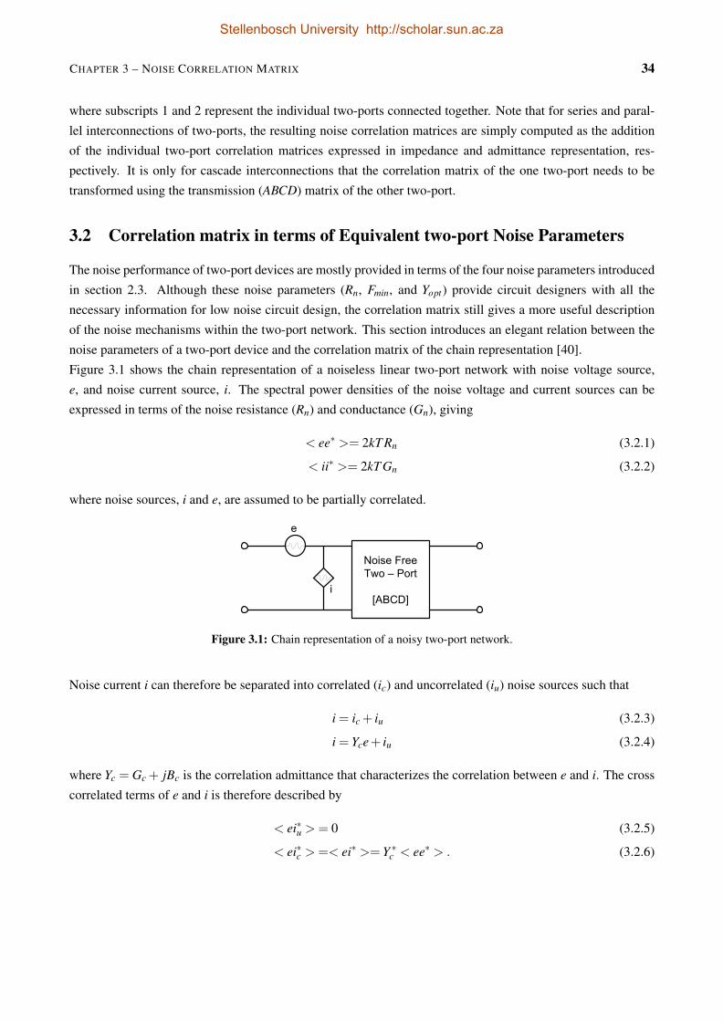
CHAPTER 3 – NOISE CORRELATION MATRIX 34
where subscripts 1 and 2 represent the individual two-ports connected together. Note that for series and paral-
lel interconnections of two-ports, the resulting noise correlation matrices are simply computed as the addition
of the individual two-port correlation matrices expressed in impedance and admittance representation, res-
pectively. It is only for cascade interconnections that the correlation matrix of the one two-port needs to be
transformed using the transmission (ABCD) matrix of the other two-port.
3.2 Correlation matrix in terms of Equivalent two-port Noise Parameters
The noise performance of two-port devices are mostly provided in terms of the four noise parameters introduced
in section 2.3. Although these noise parameters (Rn, Fmin, and Yopt) provide circuit designers with all the
necessary information for low noise circuit design, the correlation matrix still gives a more useful description
of the noise mechanisms within the two-port network. This section introduces an elegant relation between the
noise parameters of a two-port device and the correlation matrix of the chain representation [40].
Figure 3.1 shows the chain representation of a noiseless linear two-port network with noise voltage source,
e, and noise current source, i. The spectral power densities of the noise voltage and current sources can be
expressed in terms of the noise resistance (Rn) and conductance (Gn), giving
< ee∗ >= 2kT Rn (3.2.1)
< ii∗ >= 2kT Gn (3.2.2)
where noise sources, i and e, are assumed to be partially correlated.
Figure 3.1: Chain representation of a noisy two-port network.
Noise current i can therefore be separated into correlated (ic) and uncorrelated (iu) noise sources such that
i = ic + iu (3.2.3)
i = Yce+ iu (3.2.4)
where Yc = Gc + jBc is the correlation admittance that characterizes the correlation between e and i. The cross
correlated terms of e and i is therefore described by
< ei∗u >= 0 (3.2.5)
< ei∗c >=< ei∗ >= Y ∗c < ee∗ > . (3.2.6)
Stellenbosch University http://scholar.sun.ac.za

CHAPTER 3 – NOISE CORRELATION MATRIX 35
It follows from equation 3.1.1 that
C =<
[ee∗ ei∗
ie∗ ii∗
]> (3.2.7)
and therefore the correlation matrix is given by
C = 2kT
[Rn RnY ∗c
RnYc Gu +Rn |Yc|2
](3.2.8)
Figure 3.2: Linear noise free two-port shorted at the input.
If this two-port network is driven by a source with admittance Ys, the noise factor can be computed using
equation 2.3.4. In shorting the input of the linear noiseless two-port network, as shown in figure 3.2, the noise
figure as considered at the input simplifies to
F =Nss
Ni(3.2.9)
where Nss and Ni denote the short circuit and input noise powers, respectively. The output noise power is
therefore represented by the spectral power density of the short circuited current < issi∗ss > with the short circuit
noise current equal to
iss = in +Yse+ i (3.2.10)
where < ini∗n > is the spectral power density of the noise current due to the source conductance Gs
< ini∗n >= 2kT Gs (3.2.11)
and describes the input noise power. It is worth noting at this point that the noise from the source, in is
uncorrelated from the noise generated by the two-port network, e and i. The noise factor can thus be written as
F =< issi∗ss >
< ini∗n >=
< ini∗n >+< (Yse+ i)(Yse+ i)∗ >< ini∗n >
(3.2.12)
where
< (Yse+ i)(Yse+ i)∗ >=<
([Ys 1
][ e
i
])([e i
][ Ys
1
])∗> (3.2.13)
=[
Ys 1](C)
[Y ∗s1
](3.2.14)
and correlation matrix C is given by 3.2.8. Therefore the noise factor can be expressed in terms of the noise
correlation matrix and the source admittance
F = 1+1
2kT Gs
[Ys 1
]C
[Y ∗s1
](3.2.15)
Stellenbosch University http://scholar.sun.ac.za
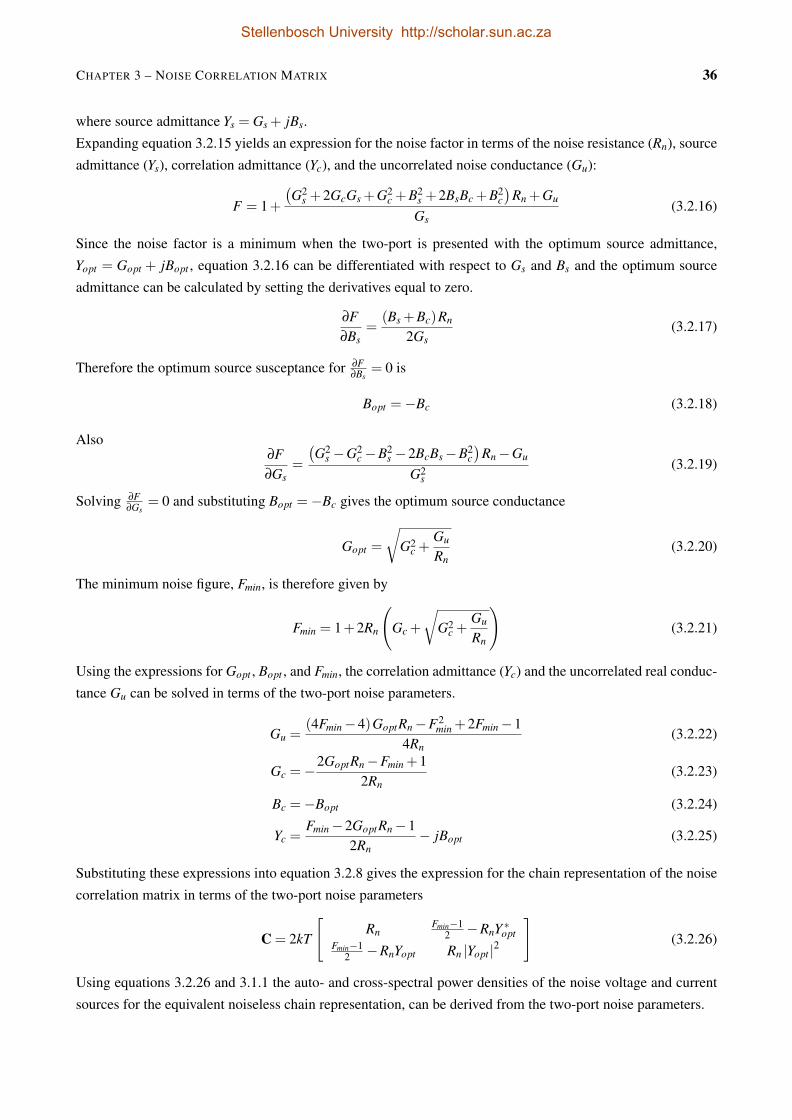
CHAPTER 3 – NOISE CORRELATION MATRIX 36
where source admittance Ys = Gs + jBs.
Expanding equation 3.2.15 yields an expression for the noise factor in terms of the noise resistance (Rn), source
admittance (Ys), correlation admittance (Yc), and the uncorrelated noise conductance (Gu):
F = 1+
(G2
s +2GcGs +G2c +B2
s +2BsBc +B2c)
Rn +Gu
Gs(3.2.16)
Since the noise factor is a minimum when the two-port is presented with the optimum source admittance,
Yopt = Gopt + jBopt , equation 3.2.16 can be differentiated with respect to Gs and Bs and the optimum source
admittance can be calculated by setting the derivatives equal to zero.
∂F∂Bs
=(Bs +Bc)Rn
2Gs(3.2.17)
Therefore the optimum source susceptance for ∂F∂Bs
= 0 is
Bopt =−Bc (3.2.18)
Also∂F∂Gs
=
(G2
s −G2c−B2
s −2BcBs−B2c)
Rn−Gu
G2s
(3.2.19)
Solving ∂F∂Gs
= 0 and substituting Bopt =−Bc gives the optimum source conductance
Gopt =
√G2
c +Gu
Rn(3.2.20)
The minimum noise figure, Fmin, is therefore given by
Fmin = 1+2Rn
(Gc +
√G2
c +Gu
Rn
)(3.2.21)
Using the expressions for Gopt , Bopt , and Fmin, the correlation admittance (Yc) and the uncorrelated real conduc-
tance Gu can be solved in terms of the two-port noise parameters.
Gu =(4Fmin−4)GoptRn−F2
min +2Fmin−14Rn
(3.2.22)
Gc =−2GoptRn−Fmin +1
2Rn(3.2.23)
Bc =−Bopt (3.2.24)
Yc =Fmin−2GoptRn−1
2Rn− jBopt (3.2.25)
Substituting these expressions into equation 3.2.8 gives the expression for the chain representation of the noise
correlation matrix in terms of the two-port noise parameters
C = 2kT
[Rn
Fmin−12 −RnY ∗opt
Fmin−12 −RnYopt Rn |Yopt |2
](3.2.26)
Using equations 3.2.26 and 3.1.1 the auto- and cross-spectral power densities of the noise voltage and current
sources for the equivalent noiseless chain representation, can be derived from the two-port noise parameters.
Stellenbosch University http://scholar.sun.ac.za
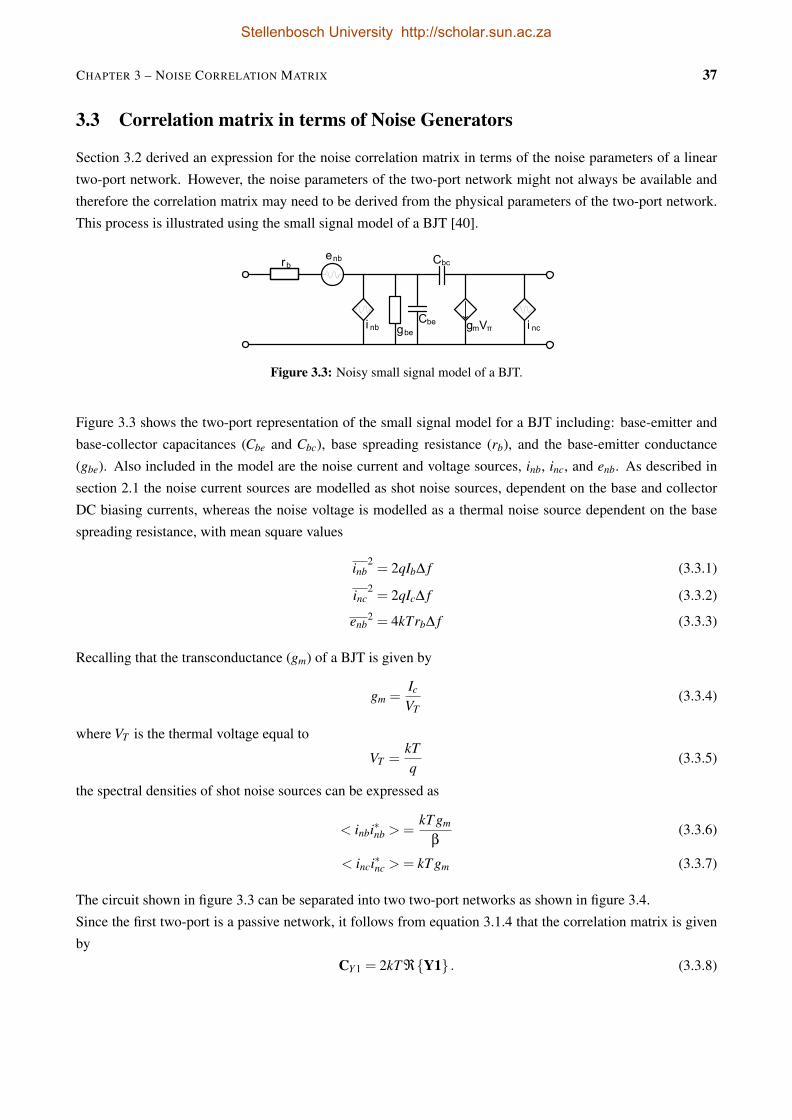
CHAPTER 3 – NOISE CORRELATION MATRIX 37
3.3 Correlation matrix in terms of Noise Generators
Section 3.2 derived an expression for the noise correlation matrix in terms of the noise parameters of a linear
two-port network. However, the noise parameters of the two-port network might not always be available and
therefore the correlation matrix may need to be derived from the physical parameters of the two-port network.
This process is illustrated using the small signal model of a BJT [40].`
`
`
`
Figure 3.3: Noisy small signal model of a BJT.
Figure 3.3 shows the two-port representation of the small signal model for a BJT including: base-emitter and
base-collector capacitances (Cbe and Cbc), base spreading resistance (rb), and the base-emitter conductance
(gbe). Also included in the model are the noise current and voltage sources, inb, inc, and enb. As described in
section 2.1 the noise current sources are modelled as shot noise sources, dependent on the base and collector
DC biasing currents, whereas the noise voltage is modelled as a thermal noise source dependent on the base
spreading resistance, with mean square values
inb2= 2qIb∆ f (3.3.1)
inc2= 2qIc∆ f (3.3.2)
enb2 = 4kTrb∆ f (3.3.3)
Recalling that the transconductance (gm) of a BJT is given by
gm =Ic
VT(3.3.4)
where VT is the thermal voltage equal to
VT =kTq
(3.3.5)
the spectral densities of shot noise sources can be expressed as
< inbi∗nb >=kT gm
β(3.3.6)
< inci∗nc >= kT gm (3.3.7)
The circuit shown in figure 3.3 can be separated into two two-port networks as shown in figure 3.4.
Since the first two-port is a passive network, it follows from equation 3.1.4 that the correlation matrix is given
by
CY 1 = 2kT ℜY1 . (3.3.8)
Stellenbosch University http://scholar.sun.ac.za
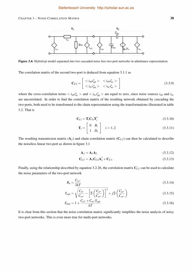
CHAPTER 3 – NOISE CORRELATION MATRIX 38
r bgbe
`
i n1i n2
`
Cbe`
Cbc`
gmVπ i nci nb
Y1 Y2
Figure 3.4: Hybrid-pi model separated into two cascaded noise free two-port networks in admittance representation.
The correlation matrix of the second two-port is deduced from equation 3.1.1 as
CY 2 =
[< inbi∗nb > < inbi∗nc >
< inci∗nb > < inci∗nc >
](3.3.9)
where the cross-correlation terms < inbi∗nc > and < inci∗nb > are equal to zero, since noise sources inb and inc
are uncorrelated. In order to find the correlation matrix of the resulting network obtained by cascading the
two-ports, both need to be transformed to the chain representation using the transformations illustrated in table
3.2. That is
CCi = TiCYiT†i (3.3.10)
Ti =
[0 Bi
1 Di
]i = 1,2 (3.3.11)
The resulting transmission matrix (A f ) and chain correlation matrix (CC f ) can then be calculated to describe
the noiseless linear two-port as shown in figure 3.1
A f = A1A2 (3.3.12)
CC f = A1CC2A†1 +CC1. (3.3.13)
Finally, using the relationship described by equation 3.2.26, the correlation matrix CC f can be used to calculate
the noise parameters of the two-port network
Rn =Cee∗
2kT(3.3.14)
Yopt =
√Cii∗
Cee∗−[
ℑ
(Cei∗
Cee∗
)]2
+ jℑ(
Cei∗
Cee∗
)(3.3.15)
Fmin = 1+Cei∗+Cee∗Yopt
kT(3.3.16)
It is clear from this section that the noise correlation matrix significantly simplifies the noise analysis of noisy
two-port networks. This is even more true for multi-port networks.
Stellenbosch University http://scholar.sun.ac.za
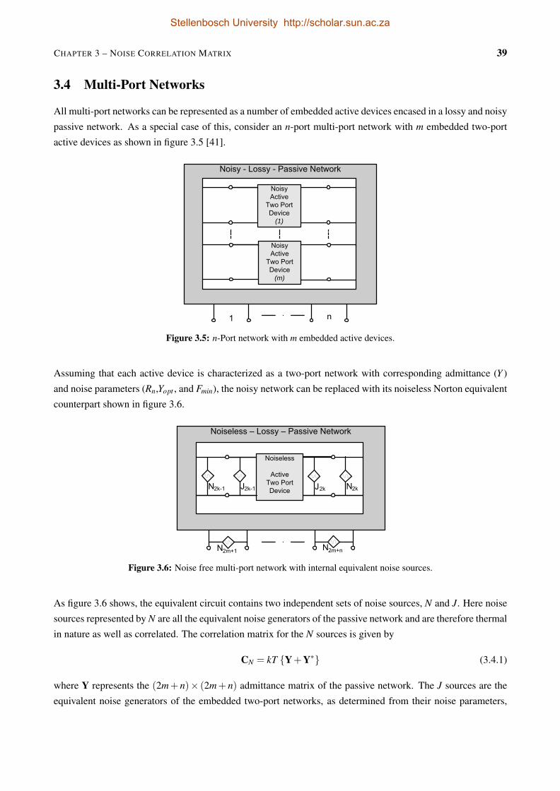
CHAPTER 3 – NOISE CORRELATION MATRIX 39
3.4 Multi-Port Networks
All multi-port networks can be represented as a number of embedded active devices encased in a lossy and noisy
passive network. As a special case of this, consider an n-port multi-port network with m embedded two-port
active devices as shown in figure 3.5 [41].
(1)
(m)
Figure 3.5: n-Port network with m embedded active devices.
Assuming that each active device is characterized as a two-port network with corresponding admittance (Y )
and noise parameters (Rn,Yopt , and Fmin), the noisy network can be replaced with its noiseless Norton equivalent
counterpart shown in figure 3.6.
Figure 3.6: Noise free multi-port network with internal equivalent noise sources.
As figure 3.6 shows, the equivalent circuit contains two independent sets of noise sources, N and J. Here noise
sources represented by N are all the equivalent noise generators of the passive network and are therefore thermal
in nature as well as correlated. The correlation matrix for the N sources is given by
CN = kT Y+Y∗ (3.4.1)
where Y represents the (2m+ n)× (2m+ n) admittance matrix of the passive network. The J sources are the
equivalent noise generators of the embedded two-port networks, as determined from their noise parameters,
Stellenbosch University http://scholar.sun.ac.za

CHAPTER 3 – NOISE CORRELATION MATRIX 40
and therefore usually not thermal in nature. Only sources from the same two-port device are assumed to be
correlated, ie. J2k−1 and J2k are correlated.
Using the given noise parameters of the embedded two-port devices, the chain representation of the correla-
tion matrix can be determined from equation 3.2.26. It is therefore necessary to derive an expression for the
admittance representation of the correlation matrix in terms of the two-port noise parameters.
(a) (b)
Figure 3.7: Chain (a) and Admittance (b) two-port representations.
Figure 3.7 depicts the required transformation. Since sources J and E are correlated
J = Ju +YcE (3.4.2)
where the subscript u represents the uncorrelated noise. Therefore, from inspection it is found that
J1 = J− y11E (3.4.3)
J2 =−y21E (3.4.4)
where y11 and y21 are admittance parameters of the embedded noiseless two-port. As defined in section 3.2
the spectral power densities of noise sources E and J are
< EE∗ >= 2kT Rn (3.4.5)
< JJ∗ >=< (Ju +YcE)(Ju +YcE)∗ >= 2kT(
Gu + |Yc|2 Rn
)(3.4.6)
Using the set of equations listed above, the correlation matrix of the admittance representation is calculated as
CJ =
[< J1J∗1 > < J1J∗2 >
< J2J∗2 > < J2J∗2 >
](3.4.7)
CJ = 2kT
[Gu + |y11−Yc|2 Rn y∗21 (y11−Yc)Rn
y21 (y11−Yc)∗Rn |y21|Rn
](3.4.8)
Note that the values of Gu and Yc are calculated from the two-port noise parameters as in equations 3.2.22 and
3.2.25, respectively.
Stellenbosch University http://scholar.sun.ac.za
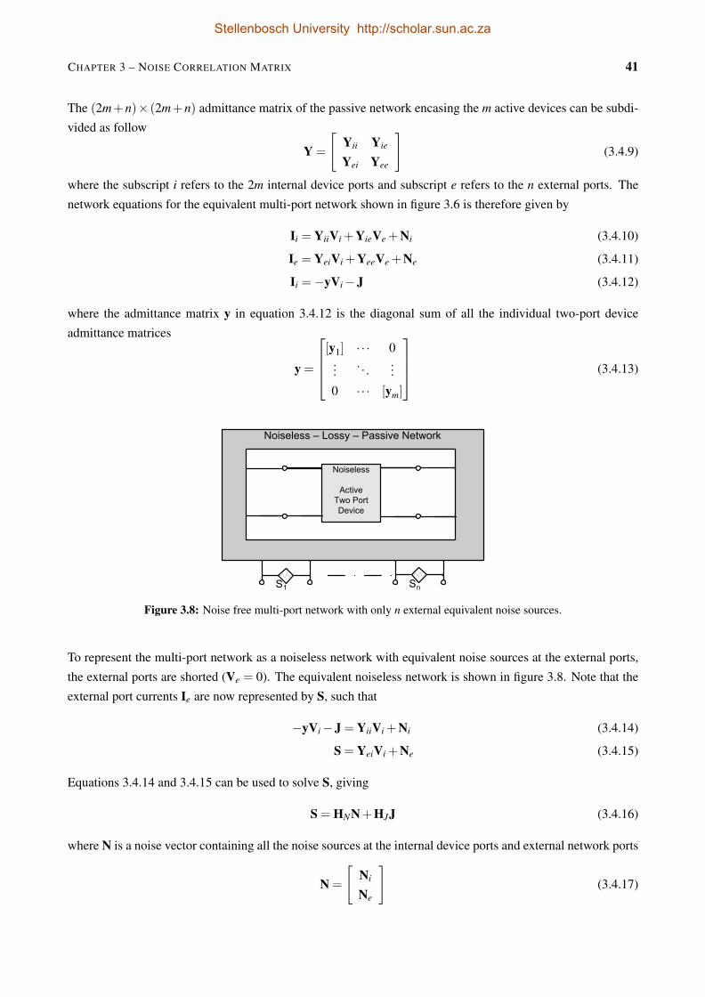
CHAPTER 3 – NOISE CORRELATION MATRIX 41
The (2m+n)× (2m+n) admittance matrix of the passive network encasing the m active devices can be subdi-
vided as follow
Y =
[Yii Yie
Yei Yee
](3.4.9)
where the subscript i refers to the 2m internal device ports and subscript e refers to the n external ports. The
network equations for the equivalent multi-port network shown in figure 3.6 is therefore given by
Ii = YiiVi +YieVe +Ni (3.4.10)
Ie = YeiVi +YeeVe +Ne (3.4.11)
Ii =−yVi−J (3.4.12)
where the admittance matrix y in equation 3.4.12 is the diagonal sum of all the individual two-port device
admittance matrices
y =
[y1] · · · 0
.... . .
...
0 · · · [ym]
(3.4.13)
Figure 3.8: Noise free multi-port network with only n external equivalent noise sources.
To represent the multi-port network as a noiseless network with equivalent noise sources at the external ports,
the external ports are shorted (Ve = 0). The equivalent noiseless network is shown in figure 3.8. Note that the
external port currents Ie are now represented by S, such that
−yVi−J = YiiVi +Ni (3.4.14)
S = YeiVi +Ne (3.4.15)
Equations 3.4.14 and 3.4.15 can be used to solve S, giving
S = HNN+HJJ (3.4.16)
where N is a noise vector containing all the noise sources at the internal device ports and external network ports
N =
[Ni
Ne
](3.4.17)
Stellenbosch University http://scholar.sun.ac.za
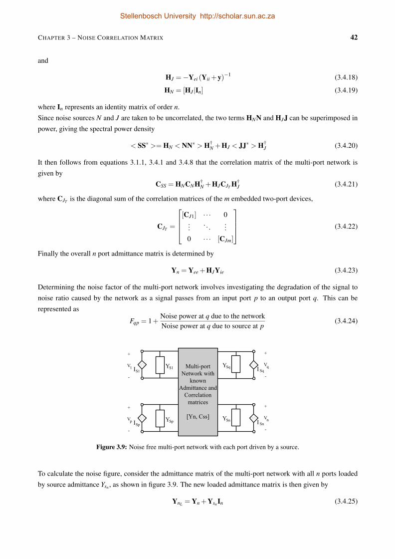
CHAPTER 3 – NOISE CORRELATION MATRIX 42
and
HJ =−Yei (Yii +y)−1 (3.4.18)
HN = [HJ|In] (3.4.19)
where In represents an identity matrix of order n.
Since noise sources N and J are taken to be uncorrelated, the two terms HNN and HJJ can be superimposed in
power, giving the spectral power density
< SS∗ >= HN < NN∗ > H†N +HJ < JJ∗ > H†
J (3.4.20)
It then follows from equations 3.1.1, 3.4.1 and 3.4.8 that the correlation matrix of the multi-port network is
given by
CSS = HNCNH†N +HJCJT H†
J (3.4.21)
where CJT is the diagonal sum of the correlation matrices of the m embedded two-port devices,
CJT =
[CJ1] · · · 0
.... . .
...
0 · · · [CJm]
(3.4.22)
Finally the overall n port admittance matrix is determined by
Yn = Yee +HJYie (3.4.23)
Determining the noise factor of the multi-port network involves investigating the degradation of the signal to
noise ratio caused by the network as a signal passes from an input port p to an output port q. This can be
represented as
Fqp = 1+Noise power at q due to the networkNoise power at q due to source at p
(3.4.24)
Figure 3.9: Noise free multi-port network with each port driven by a source.
To calculate the noise figure, consider the admittance matrix of the multi-port network with all n ports loaded
by source admittance Ysn , as shown in figure 3.9. The new loaded admittance matrix is then given by
YnL = Yn +YsnIn (3.4.25)
Stellenbosch University http://scholar.sun.ac.za
CHAPTER 3 – NOISE CORRELATION MATRIX 43
and the loaded impedance matrix of the n port network is simply the inverse
ZnL = (YnL)−1 =
Ze1
Ze2...
Zen
(3.4.26)
where Zen denotes a row vector described by
Zen =[Zn1 Zn2 · · ·
](3.4.27)
Consider the noise power delivered to port q due to the network. The voltage at port q, Vq is represented by the
vector equation
[Vq] =− [Zeq] [S] (3.4.28)
with S being the vector containing the n external equivalent noise sources as described in equation 3.4.16. The
noise power due to the network delivered to port q is then given by
Pqn =< VqV∗q > ℜ
Ysq
(3.4.29)
and, since
< VqV∗q >= Zeq < SS∗ > Z†eq (3.4.30)
the noise power Pqn can be expressed in terms of the noise correlation matrix
Pqn = [Zeq]2CSS [Zeq]†
ℜ
Ysq
(3.4.31)
The noise power at port q due to the source at port p is equal to
Pqp =< VqpV∗qp > ℜ
Ysq
(3.4.32)
where the mean square of the noise voltage Vqp produced at port q, due to the noise source input isp at port p, is
given by
<VqpV ∗qp >=∣∣Zqp
∣∣2 < ispi∗sp > (3.4.33)
Noting that the spectral power density of the noise source at port p is equal to
< ispi∗sp >= 2kT ℜYsp (3.4.34)
the noise power due to the noise source at port p can be expressed by
Pqp =∣∣Zqp
∣∣2 4kT ℜYspℜ
Ysq
(3.4.35)
The noise figure calculated from port p to port q is therefore solved, in terms of the multi-port noise correlation
matrix, by
Fqp = 1+[Zeq]CSS [Zeq]
†∣∣Zqp∣∣2 4kT ℜYsp
(3.4.36)
When a network consists of multiple input and output ports differential- and common-mode (mixed-mode)
signals can propagate between coupled ports (The theory of mixed-mode signal propagation is discussed in
Chapter 4). Using the noise correlation matrix, three- or four-port networks can be transformed into two equi-
valent noiseless two-port networks, one for each mode of propagation. Section 6.2.6 derives the differential
noise parameters of a three-port network by means of the mixed-mode correlation matrix.
Stellenbosch University http://scholar.sun.ac.za
CHAPTER 3 – NOISE CORRELATION MATRIX 44
3.5 Conclusion
This chapter illustrates the importance of the noise correlation matrix when investigating the noise performance
of both two-port and multi-port networks. The three two-port representations introduced in section 3.1 make
this theory applicable to any noisy linear two-port network and the transformations summarised in table 3.2
significantly simplifies two-port noise analysis by allowing networks to be considered as the interconnection of
simpler two-port networks. Lastly the direct relationship between the noise parameters of a two-port device and
the elements of the correlation matrix of the chain representation proves to be extremely useful when analysing
the noise performance of mixed-mode propagation in multi-port networks (refer to chapter 6).
Stellenbosch University http://scholar.sun.ac.za

Chapter 4
Transmission Line Theory
Single-ended circuits operating at microwave frequencies are commonly characterised by their Scattering (S)-
parameters. When working with differential circuits, the important characteristics are however in terms of
combinations of standard S-parameters. A number of advantages can be achieved by defining an alternative set
of S-parameters, the so called Mixed-Mode S-paramters. Bockelman and Eisenstadt were the first to introduce
mixed-mode S-parameters for differential circuits, based on the two propagation modes that co-exist on pairs of
coupled transmission lines [42]. This chapter applies general transmission line theory to coupled transmission
lines in order to derive expressions for the differential- and common-mode waves propagating on the lines.
These expressions are then used to find a transformation matrix that can be used to transform the general S-
parameters of a four-port network into the equivalent mixed-mode S-parameters.
4.1 Generalized Scattering Parameters
Measuring the voltages and currents of microwave networks and their related impedance and admittance ma-
trices can prove to be a difficult task, since it involves the measurement of the magnitude and phase of a wave
propagating in a certain direction. Scattering parameters, on the other hand, relate the incident voltage waves
at the network ports to the waves reflected from the ports and can easily be calculated using network analysis
techniques or measured using a vector network analyzer. To derive expressions for the S-parameters, consider
the N-port network, shown in figure 4.1, with arbitrary characteristic impedances [15]. The port voltages and
currents can be defined in terms of their incident and reflected components. That is,
Vn =V+n +V−n (4.1.1)
In = I+n − I−n (4.1.2)
where the superscripts + and − indicate the incident and reflected waves, respectively. Given that the incident
and reflected voltage and current are related to one another by,
V+n = Z∗0n
I+n (4.1.3)
V−n = Z0nI−n (4.1.4)
45
Stellenbosch University http://scholar.sun.ac.za
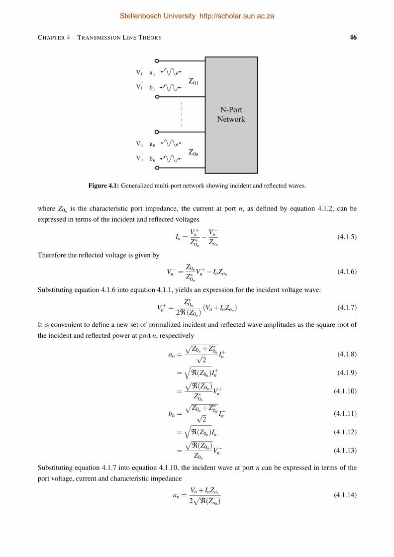
CHAPTER 4 – TRANSMISSION LINE THEORY 46
1
1
1+
1-
n
n
n+
n-
Figure 4.1: Generalized multi-port network showing incident and reflected waves.
where Z0n is the characteristic port impedance, the current at port n, as defined by equation 4.1.2, can be
expressed in terms of the incident and reflected voltages
In =V+
n
Z∗0n
− V−nZon
(4.1.5)
Therefore the reflected voltage is given by
V−n =Z0n
Z∗0n
V+n − InZon (4.1.6)
Substituting equation 4.1.6 into equation 4.1.1, yields an expression for the incident voltage wave:
V+n =
Z∗0n
2ℜ(Z0n)(Vn + InZon) (4.1.7)
It is convenient to define a new set of normalized incident and reflected wave amplitudes as the square root of
the incident and reflected power at port n, respectively
an =
√Z0n +Z∗0n√
2I+n (4.1.8)
=√
ℜ(Z0n)I+n (4.1.9)
=
√ℜ(Z0n)
Z∗0n
V+n (4.1.10)
bn =
√Z0n +Z∗0n√
2I−n (4.1.11)
=√
ℜ(Z0n)I−n (4.1.12)
=
√ℜ(Z0n)
Z0n
V−n (4.1.13)
Substituting equation 4.1.7 into equation 4.1.10, the incident wave at port n can be expressed in terms of the
port voltage, current and characteristic impedance
an =Vn + InZon
2√
ℜ(Zon)(4.1.14)
Stellenbosch University http://scholar.sun.ac.za
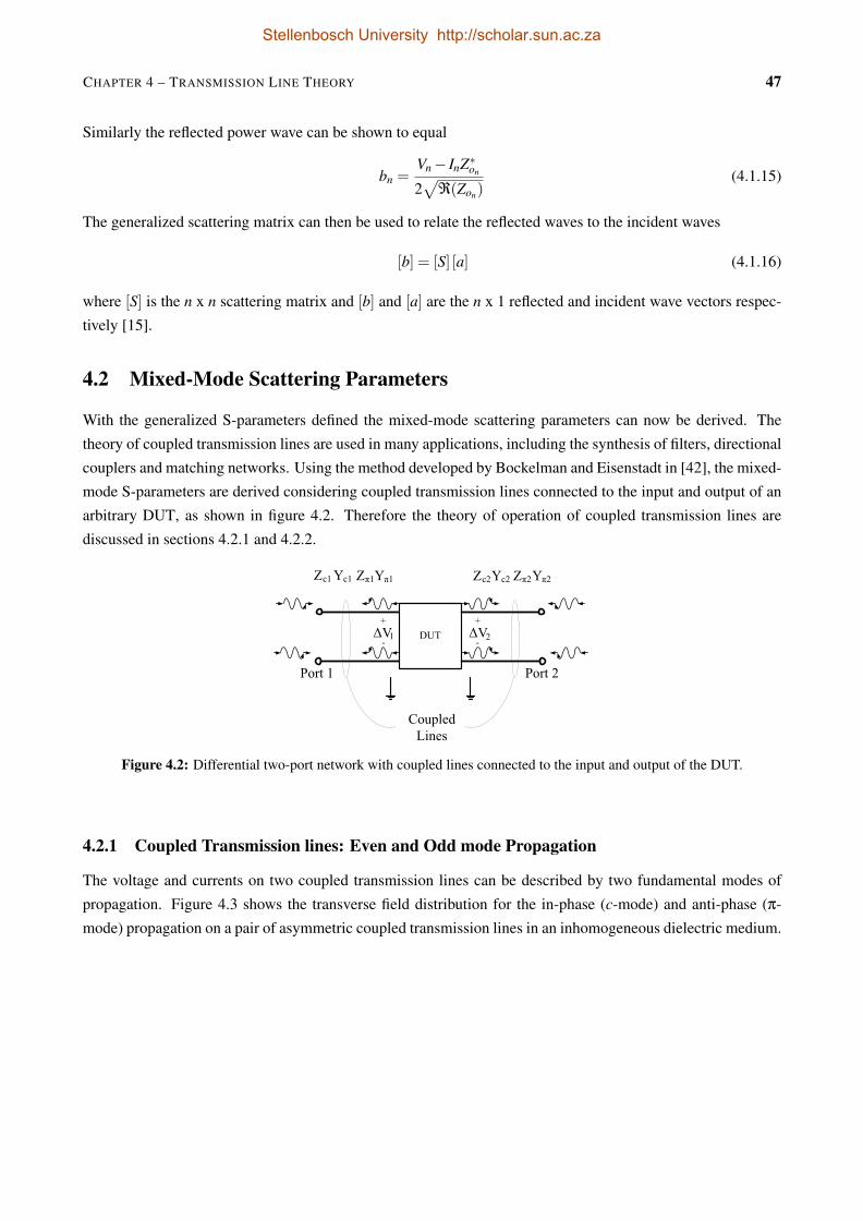
CHAPTER 4 – TRANSMISSION LINE THEORY 47
Similarly the reflected power wave can be shown to equal
bn =Vn− InZ∗on
2√
ℜ(Zon)(4.1.15)
The generalized scattering matrix can then be used to relate the reflected waves to the incident waves
[b] = [S] [a] (4.1.16)
where [S] is the n x n scattering matrix and [b] and [a] are the n x 1 reflected and incident wave vectors respec-
tively [15].
4.2 Mixed-Mode Scattering Parameters
With the generalized S-parameters defined the mixed-mode scattering parameters can now be derived. The
theory of coupled transmission lines are used in many applications, including the synthesis of filters, directional
couplers and matching networks. Using the method developed by Bockelman and Eisenstadt in [42], the mixed-
mode S-parameters are derived considering coupled transmission lines connected to the input and output of an
arbitrary DUT, as shown in figure 4.2. Therefore the theory of operation of coupled transmission lines are
discussed in sections 4.2.1 and 4.2.2.
DUT1-
+
2-
+
π1 π2 π2π1c1 c1 c2 c2
Figure 4.2: Differential two-port network with coupled lines connected to the input and output of the DUT.
4.2.1 Coupled Transmission lines: Even and Odd mode Propagation
The voltage and currents on two coupled transmission lines can be described by two fundamental modes of
propagation. Figure 4.3 shows the transverse field distribution for the in-phase (c-mode) and anti-phase (π-
mode) propagation on a pair of asymmetric coupled transmission lines in an inhomogeneous dielectric medium.
Stellenbosch University http://scholar.sun.ac.za
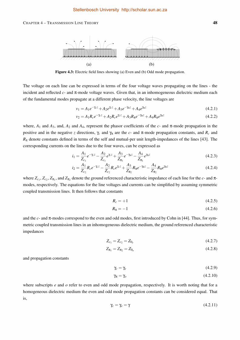
CHAPTER 4 – TRANSMISSION LINE THEORY 48
(a) (b)
Figure 4.3: Electric field lines showing (a) Even and (b) Odd mode propagation.
The voltage on each line can be expressed in terms of the four voltage waves propagating on the lines - the
incident and reflected c- and π-mode voltage waves. Given that, in an inhomogeneous dielectric medium each
of the fundamental modes propagate at a different phase velocity, the line voltages are
v1 = A1e−γcz +A2eγcz +A3e−γπz +A4eγπz (4.2.1)
v2 = A1Rce−γcz +A2Rceγcz +A3Rπe−γπz +A4Rπeγπz (4.2.2)
where, A1 and A3, and, A2 and A4, represent the phasor coefficients of the c- and π-mode propagation in the
positive and in the negative z directions, γc and γπ are the c- and π-mode propagation constants, and Rc and
Rπ denote constants defined in terms of the self and mutual-per unit length-impedances of the lines [43]. The
corresponding currents on the lines due to the four waves, can be expressed as
i1 =A1
Zc1
e−γcz− A2
Zc1
eγcz +A3
Zπ1
e−γπz− A4
Zπ1
eγπz (4.2.3)
i2 =A1
Zc2
Rce−γcz− A2
Zc2
Rceγcz +A3
Zπ2
Rπe−γπz− A4
Zπ2
Rπeγπz (4.2.4)
where Zc1 , Zc2 , Zπ1 , and Zπ2 denote the ground referenced characteristic impedance of each line for the c- and π-
modes, respectively. The equations for the line voltages and currents can be simplified by assuming symmetric
coupled transmission lines. It then follows that constants
Rc =+1 (4.2.5)
Rπ =−1 (4.2.6)
and the c- and π-modes correspond to the even and odd modes, first introduced by Cohn in [44]. Thus, for sym-
metric coupled transmission lines in an inhomogeneous dielectric medium, the ground referenced characteristic
impedances
Zc1 = Zc2 = Z0e (4.2.7)
Zπ1 = Zπ2 = Z0o (4.2.8)
and propagation constants
γc = γe (4.2.9)
γπ = γo (4.2.10)
where subscripts e and o refer to even and odd mode propagation, respectively. It is worth noting that for a
homogeneous dielectric medium the even and odd mode propagation constants can be considered equal. That
is,
γc = γe = γ (4.2.11)
Stellenbosch University http://scholar.sun.ac.za
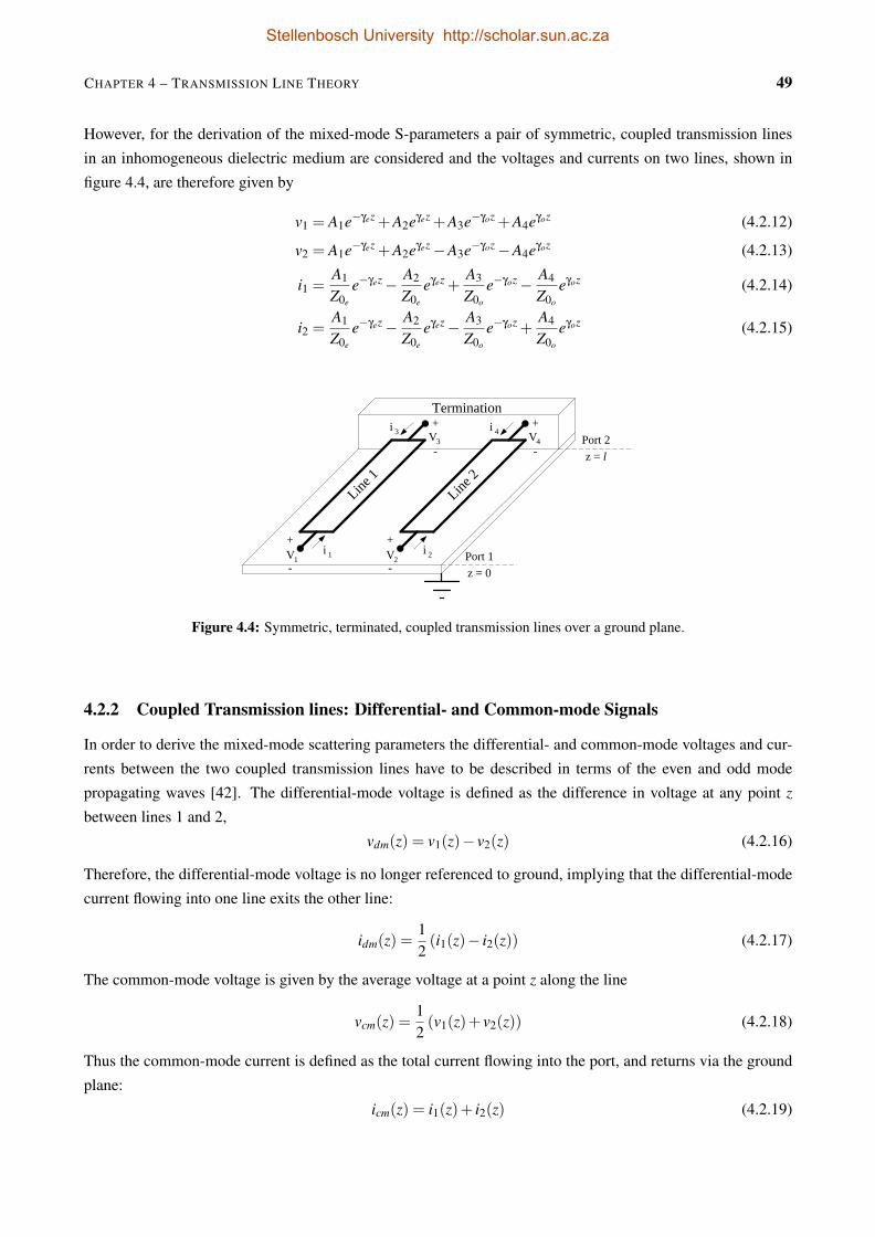
CHAPTER 4 – TRANSMISSION LINE THEORY 49
However, for the derivation of the mixed-mode S-parameters a pair of symmetric, coupled transmission lines
in an inhomogeneous dielectric medium are considered and the voltages and currents on two lines, shown in
figure 4.4, are therefore given by
v1 = A1e−γez +A2eγez +A3e−γoz +A4eγoz (4.2.12)
v2 = A1e−γez +A2eγez−A3e−γoz−A4eγoz (4.2.13)
i1 =A1
Z0e
e−γez− A2
Z0e
eγez +A3
Z0o
e−γoz− A4
Z0o
eγoz (4.2.14)
i2 =A1
Z0e
e−γez− A2
Z0e
eγez− A3
Z0o
e−γoz +A4
Z0o
eγoz (4.2.15)
z = 0
z = l
+
-
+
-
+
-
+
-
V1 V2
V4V3
Port 1
Port 2i 4i 3
i 2i 1
Termination
Line 2
Line 1
Figure 4.4: Symmetric, terminated, coupled transmission lines over a ground plane.
4.2.2 Coupled Transmission lines: Differential- and Common-mode Signals
In order to derive the mixed-mode scattering parameters the differential- and common-mode voltages and cur-
rents between the two coupled transmission lines have to be described in terms of the even and odd mode
propagating waves [42]. The differential-mode voltage is defined as the difference in voltage at any point z
between lines 1 and 2,
vdm(z) = v1(z)− v2(z) (4.2.16)
Therefore, the differential-mode voltage is no longer referenced to ground, implying that the differential-mode
current flowing into one line exits the other line:
idm(z) =12(i1(z)− i2(z)) (4.2.17)
The common-mode voltage is given by the average voltage at a point z along the line
vcm(z) =12(v1(z)+ v2(z)) (4.2.18)
Thus the common-mode current is defined as the total current flowing into the port, and returns via the ground
plane:
icm(z) = i1(z)+ i2(z) (4.2.19)
Stellenbosch University http://scholar.sun.ac.za

CHAPTER 4 – TRANSMISSION LINE THEORY 50
Let v fo(z) and vr
o(z) represent the forward and reverse propagating odd mode waves respectively and v fe (z) and
vre(z) the forward and reverse propagating even mode waves:
v fe (z) = A1e−γez (4.2.20)
vre(z) = A2eγez (4.2.21)
v fo(z) = A3e−γoz (4.2.22)
vro(z) = A4eγoz (4.2.23)
Similarly, from equations 4.2.14 and 4.2.15
i fe (z) =
A1
Z0e
e−γez (4.2.24)
ire(z) =A2
Z0e
eγez (4.2.25)
i fo(z) =
A3
Z0o
e−γoz (4.2.26)
iro(z) =A4
Z0o
eγez (4.2.27)
From equations 4.2.12 to 4.2.15, the differential-mode voltage and current defined in equations 4.2.16 and
4.2.17 can be expressed as:
vdm(z) = 2[v f
o(z)+ vro(z)]
(4.2.28)
idm(z) =1
Z0o
[v f
o(z)− vro(z)]
(4.2.29)
Also, the common-mode voltage and current expressed by equations 4.2.18 and 4.2.19 are given by
vcm(z) =[v f
e (z)+ vre(z)]
(4.2.30)
icm(z) =2
Z0e
[v f
e (z)− vre(z)]
(4.2.31)
It can be noted from the above sets of equations that differential-mode signals are only defined by odd mode
propagation whereas common-mode signals are only defined by even-mode propagation.
Considering only the forward propagating part of the differential- and common-mode voltages and currents, the
differential- and common-mode characteristic impedances can be determined in terms of the ground referenced
even and odd mode characteristic impedances:
Zdm =v f
dm
i fdm
= 2Z0o (4.2.32)
Zcm =v f
cm
i fcm
=Z0e
2(4.2.33)
It should also be noted that, in general, the even and odd mode characteristic impedances are not equal.
With the differential- and common-mode voltages, currents, and characteristic impedances defined, the mixed-
mode power waves at the nth port can be defined. In a similar fashion to equations 4.1.14 and 4.1.15 the
amplitude of the differential wave propagating in the positive z direction can be expressed as
admn |z=0 =1
2√
ℜ(Zdm)[vdm(z)+ idm(z)Zdm] |z=0 (4.2.34)
Stellenbosch University http://scholar.sun.ac.za

CHAPTER 4 – TRANSMISSION LINE THEORY 51
and the differential wave propagating in the negative z direction as
bdmn |z=0 =1
2√
ℜ(Zdm)[vdm(z)− idm(z)Z∗dm] |z=0 (4.2.35)
Similarly, the common-mode waves at port n are
acmn |z=0 =1
2√
ℜ(Zcm)[vcm(z)+ icm(z)Zcm]z=0 (4.2.36)
bcmn |z=0 =1
2√
ℜ(Zcm)[vcm(z)− icm(z)Z∗cm] |z=0 (4.2.37)
As done in section 4.1, the mixed mode reflected waves at ports 1 and 2 of the differential network shown in
figure 4.2, can be related to the incident waves by means of the mixed-mode scattering matrix,bdm1
bdm2
bcm1
bcm2
=
[Sdd Sdc
Scd Scc
]adm1
adm2
acm1
acm2
(4.2.38)
where Sdd denotes the differential-mode S-parameters, Scc denotes the common-mode S-parameters, and Scd
and Sdc the cross-mode S-parameters describing the conversion of differential-mode signals into common-mode
signals and vice versa.
Thus, the differential two port, consisting of four terminals, can be described in terms of the mixed-mode
scattering parameters [45]:
[bmm] = [Smm] [amm] (4.2.39)
where bmm and amm are the 4 x 1 reflected and incident mixed-mode wave vectors as used in equation 4.2.38,
and Smm is the 4 x 4 mixed-mode S-parameter matrix.
4.3 Mixed-mode Scattering Parameters derived from General ScatteringParameters
In many circuits, differential circuits are not driven by coupled lines. To analyse this, the distance between the
two coupled lines is increased to infinity, resulting in
Z0e = Z0o = Z0 (4.3.1)
where Z0 is the characteristic impedance of one line. From equations 4.1.14 and 4.1.15 the normalized incident
and reflected waves at each terminal are given by
ai =1
2√
ℜ(Z0)[vi + iiZ0] (4.3.2)
bi =1
2√
ℜ(Z0)[vi− iiZ∗0 ] (4.3.3)
Stellenbosch University http://scholar.sun.ac.za
CHAPTER 4 – TRANSMISSION LINE THEORY 52
where i = 1,2,3,4. and similar to section 4.2.1, the line voltage and current equations for Port 1 at z = 0 are
v1(z) = v fe (z)+ vr
e(z)+ v fo(z)+ vr
o(z) (4.3.4)
v2(z) = v fe (z)+ vr
e(z)− v fo(z)− vr
o(z) (4.3.5)
i1(z) =1Z0
[v f
e (z)− vre(z)+ v f
o(z)− vro(z)]
(4.3.6)
i2(z) =1Z0
[v f
e (z)− vre(z)− v f
o(z)+ vro(z)]
(4.3.7)
The incident and reflected waves of terminals 1 and 2, at Port 1, can therefore be expressed as
a1|z=0 =1
2√
ℜ(Z0)[v1 + i1Z0]
=1
2√
ℜ(Z0)
[2(v f
e (z)+ v fo(z)
)](4.3.8)
b1|z=0 =1
2√
ℜ(Z0)[v1− i1Z∗0 ]
=1
2√
ℜ(Z0)[2(vr
e(z)+ vro(z))] (4.3.9)
a2|z=0 =1
2√
ℜ(Z0)[v2 + i2Z0]
=1
2√
ℜ(Z0)
[2(v f
e (z)− v fo(z)
)](4.3.10)
b2|z=0 =1
2√
ℜ(Z0)[v2− i2Z∗0 ]
=1
2√
ℜ(Z0)[2(vr
e(z)− vro(z))] (4.3.11)
Furthermore, the differential and common-mode voltages and currents at Port 1 are:
vdm(z) = 2[v f
o(z)+ vro(z)]
(4.3.12)
idm(z) =1Z0
[v f
o(z)− vro(z)]
(4.3.13)
vcm(z) =[v f
e (z)+ vre(z)]
(4.3.14)
icm(z) =2Z0
[v f
e (z)− vre(z)]
(4.3.15)
Substituting these values into the equations for the differential- and common-mode power waves, yields the
expressions for the differential- and common-mode incident and reflected power waves at Port 1, in terms of
the propagating waves at terminals 1 and 2. Hence, the incident and reflected differential waves at Port 1, given
by equation 4.2.34 and 4.2.35, equals
adm1 |z=0 =1
2√
Zdm
[v f
o(z)(
2+Zdm
Z0
)+ vr
o(z)(
2− Zdm
Z0
)]|z=0 (4.3.16)
bdm1 |z=0 =1
2√
Zdm
[vr
o(z)(
2+Z∗dmZ0
)+ v f
o(z)(
2−Z∗dmZ0
)]|z=0 (4.3.17)
Stellenbosch University http://scholar.sun.ac.za
CHAPTER 4 – TRANSMISSION LINE THEORY 53
It then follows from equation 4.3.17 that the characteristic port impedance has to be real, such that the forward
propagating voltage equals zero when considering reflected waves. Therefore, given that,
Z0 = R0 (4.3.18)
Zdm = 2R0 (4.3.19)
Zcm =R0
2(4.3.20)
equations 4.3.16 and 4.3.17 reduce to
adm1 =1
2√
2R0
(4v f
o)
=1√2(a1−a2) (4.3.21)
bdm1 =1
2√
2R0(4vr
o)
=1√2(b1−b2) (4.3.22)
Also, since Zcm = R02 , the incident and reflected common-mode power wave at Port 1, given by equations 4.2.36
and 4.2.37 reduce to
acm1 |z=0 =1√2R0
[2(v f
e (z))]|z=0
=1√2[a1 +a2] (4.3.23)
bcm1 |z=0 =1√2R0
[2(vre(z))] |z=0
=1√2[b1 +b2] (4.3.24)
The above equations clearly indicate that the differential- and common-mode incident waves are defined by the
forward propagating odd and even mode waves, while the reflected waves are defined by the reverse directed
odd and even mode propagation, respectively. Repeating the above procedure at z = l the mixed-mode power
waves at Port 2, comprising of terminals 3 and 4, are shown to be
adm2 =1√2[a3−a4] (4.3.25)
bdm2 =1√2[b3−b4] (4.3.26)
acm2 =1√2[a3 +a4] (4.3.27)
bcm2 =1√2[b3 +b4] (4.3.28)
It then follows from equations 4.3.22, 4.3.26, 4.3.24, and 4.3.28 that the reflected mixed-mode waves at each
port can be related to the reflected waves at each terminal:
[bmm] = [M] [b] (4.3.29)
Stellenbosch University http://scholar.sun.ac.za

CHAPTER 4 – TRANSMISSION LINE THEORY 54
where,
[M] =1√2
1 −1 0 0
0 0 1 −1
1 1 0 0
0 0 1 1
(4.3.30)
is the transformation matrix and [b] =[b1, b2, b3, b4
]Tis the reflected waves at the four terminals as
defined in equation 4.1.16.
Similarly it can be shown that
[amm] = [M] [a] (4.3.31)
where [a] =[a1, a2, a3, a4
]Tis the vector containing the incident waves at each of the four terminals.
Thus, from equations 4.1.16, 4.3.29, and 4.3.31 we can relate the standard four terminal scattering matrix [S]
and the mixed-mode scattering matrix [Smm] by
[Smm] = [M] [S] [M]−1 (4.3.32)
[S] = [M]−1 [Smm] [M] (4.3.33)
4.4 Conclusion
This chapter introduced a method of obtaining the mixed-mode S-parameters of a differential network from a
standard S-parameters measurement. This makes it possible to determine the differential and common-mode
gain as well as the common-mode rejection ratio of a differential network using the general S-parameters of the
network. Furthermore, the techniques for deriving the mixed-mode parameters can be applied to mixed-mode
noise analysis, as done in section 6.2.6, wherein a transformation matrix analogous to that of equation 4.3.30 is
derived in order to calculate the differential noise parameters of a differential network.
Stellenbosch University http://scholar.sun.ac.za
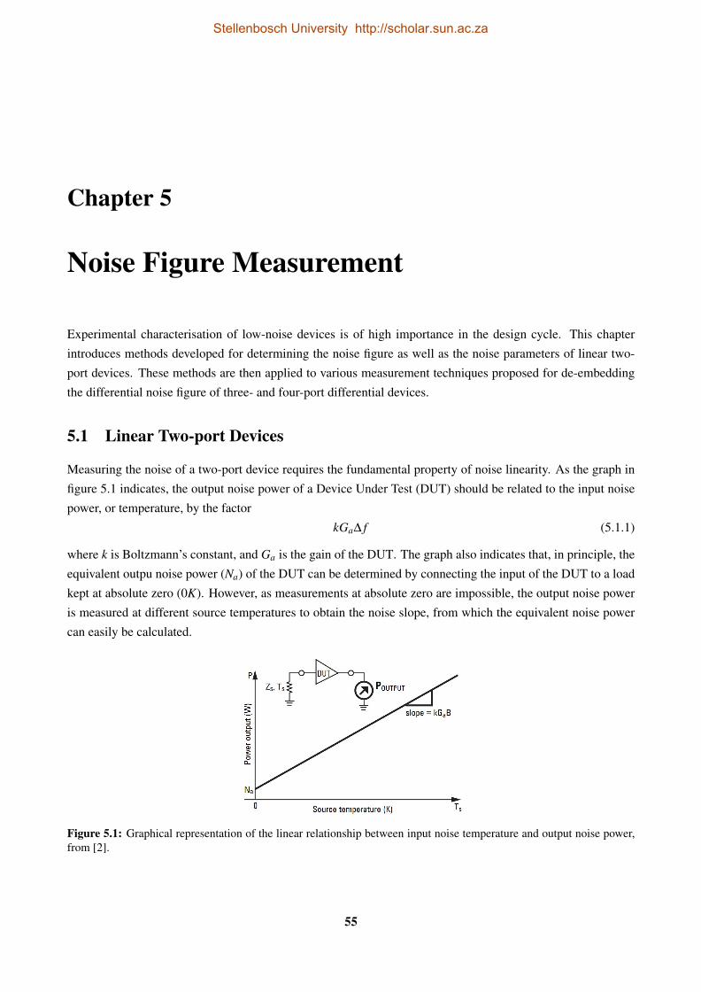
Chapter 5
Noise Figure Measurement
Experimental characterisation of low-noise devices is of high importance in the design cycle. This chapter
introduces methods developed for determining the noise figure as well as the noise parameters of linear two-
port devices. These methods are then applied to various measurement techniques proposed for de-embedding
the differential noise figure of three- and four-port differential devices.
5.1 Linear Two-port Devices
Measuring the noise of a two-port device requires the fundamental property of noise linearity. As the graph in
figure 5.1 indicates, the output noise power of a Device Under Test (DUT) should be related to the input noise
power, or temperature, by the factor
kGa∆ f (5.1.1)
where k is Boltzmann’s constant, and Ga is the gain of the DUT. The graph also indicates that, in principle, the
equivalent outpu noise power (Na) of the DUT can be determined by connecting the input of the DUT to a load
kept at absolute zero (0K). However, as measurements at absolute zero are impossible, the output noise power
is measured at different source temperatures to obtain the noise slope, from which the equivalent noise power
can easily be calculated.
Figure 5.1: Graphical representation of the linear relationship between input noise temperature and output noise power,from [2].
55
Stellenbosch University http://scholar.sun.ac.za
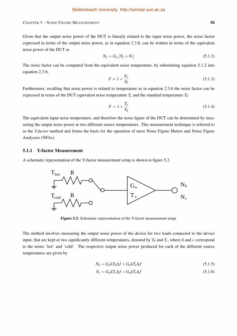
CHAPTER 5 – NOISE FIGURE MEASUREMENT 56
Given that the output noise power of the DUT is linearly related to the input noise power, the noise factor
expressed in terms of the output noise power, as in equation 2.3.8, can be written in terms of the equivalent
noise power of the DUT as
Na = Ga (Ne +Ni) (5.1.2)
The noise factor can be computed from the equivalent noise temperature, by substituting equation 5.1.2 into
equation 2.3.8,
F = 1+Ne
Ni(5.1.3)
Furthermore, recalling that noise power is related to temperature as in equation 2.3.6 the noise factor can be
expressed in terms of the DUT equivalent noise temperature Te and the standard temperature T0
F = 1+Te
T0(5.1.4)
The equivalent input noise temperature, and therefore the noise figure of the DUT can be determined by mea-
suring the output noise power at two different source temperatures. This measurement technique is referred to
as the Y-factor method and forms the basis for the operation of most Noise Figure Meters and Noise Figure
Analysers (NFAs).
5.1.1 Y-factor Measurement
A schematic representation of the Y-factor measurement setup is shown in figure 5.2.
Thot
Tcold
R
R T e
Ga Nh
Nc
Figure 5.2: Schematic representation of the Y-factor measurement setup.
The method involves measuring the output noise power of the device for two loads connected to the device
input, that are kept at two significantly different temperatures, denoted by Th and Tc, where h and c correspond
to the terms ’hot’ and ’cold’. The respective output noise power produced for each of the different source
temperatures are given by
Nh = GakTh∆ f +GakTe∆ f (5.1.5)
Nc = GakTc∆ f +GakTe∆ f (5.1.6)
Stellenbosch University http://scholar.sun.ac.za
CHAPTER 5 – NOISE FIGURE MEASUREMENT 57
Using the output noise powers, the Y-factor is defined as
Y =Nh
Nc=
Th +Te
Tc +Te> 1 (5.1.7)
from which the equivalent noise temperature of the DUT can be solved as
Te =Th−Y Tc
Y −1(5.1.8)
Considering equations 5.1.7 and 5.1.8, it is clear that the temperature difference of the two noise sources
should be large enough to avoid unnecessary loss of accuracy [15]. Therefore, when performing the Y-factor
measurements manually, one load is usually kept at room temperature (Th = T0 = 290K), while the other is
immersed in either liquid Nitrogen (Tc = 77K) or Helium (Tc = 4K). Since manual Y-factor measurement
requires an accurate temperature controlled environment to ensure repeatable results, noise figure measurement
is mostly performed using modern Noise Figure Meters or NFAs that use electronic noise sources. One of the
noise sources generally used in noise figure measurements is a low-capacitance diode that generates noise levels
equivalent to several thousand Kelvin when reverse biased into avalanche breakdown, referred to as the noise
source’s ’ON’ state [2]. In its ’OFF’ state the noise source produces a noise temperature equal to the ambient
temperature. The output noise level of a noise source is represented by its ENR which is expressed, in dB, as
ENRdB = 10log(
Th−Tc
T0
)(5.1.9)
Noise sources are each supplied with their unique dataset containing the calibrated ENR values over a frequency
range. Note that the calibration of a noise source is performed in a controlled environment to ensure Tc = T0 =
290K and it is therefore necessary to compensate for any deviation of Tc from T0 during measurements. This
procedure can be avoided by performing measurements using a noise source similar to Agilent’s SNS-Series
that incorporates a temperature sensor and transmits the value of Tc to the NFA before each measurement sweep,
thereby increasing the accuracy of the measured data. Further techniques of improving measurement accuracy
are discussed in the following section.
5.1.2 Measurement Accuracy Improvement
Performing noise measurement with a NFA involves a two step procedure: a calibration of the measurement
system and the actual noise figure measurement of the DUT. During both the calibration and the measurement
procedure, the NFA performs noise analysis based on the Y-factor method introduced in section 5.1.1. The NFA
computes the gain (GNFA) and noise figure (FNFA) of the measurement system during the calibration procedure,
and stores the ’hot’ and ’cold’ output noise powers NONc and NOFF
c . Repeating the procedure with the DUT in
place, the NFA measures the system output noise powers NONs and NOFF
s and computes the gain of the DUT as
the ratio
GDUT =NON
s −NOFFs
NONc −NOFF
c(5.1.10)
and the system noise figure Fsys using the Y-factor method.
Stellenbosch University http://scholar.sun.ac.za
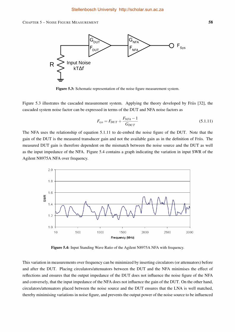
CHAPTER 5 – NOISE FIGURE MEASUREMENT 58
Input NoisekT∆f
R
GDUT GNFAFDUT FNFA
FSys
Figure 5.3: Schematic representation of the noise figure measurement system.
Figure 5.3 illustrates the cascaded measurement system. Applying the theory developed by Friis [32], the
cascaded system noise factor can be expressed in terms of the DUT and NFA noise factors as
Fsys = FDUT +FNFA−1
GDUT(5.1.11)
The NFA uses the relationship of equation 5.1.11 to de-embed the noise figure of the DUT. Note that the
gain of the DUT is the measured transducer gain and not the available gain as in the definition of Friis. The
measured DUT gain is therefore dependent on the mismatch between the noise source and the DUT as well
as the input impedance of the NFA. Figure 5.4 contains a graph indicating the variation in input SWR of the
Agilent N8975A NFA over frequency.
Figure 5.4: Input Standing Wave Ratio of the Agilent N8975A NFA with frequency.
This variation in measurements over frequency can be minimized by inserting circulators (or attenuators) before
and after the DUT. Placing circulators/attenuators between the DUT and the NFA minimises the effect of
reflections and ensures that the output impedance of the DUT does not influence the noise figure of the NFA
and conversely, that the input impedance of the NFA does not influence the gain of the DUT. On the other hand,
circulators/attenuators placed between the noise source and the DUT ensures that the LNA is well matched,
thereby minimising variations in noise figure, and prevents the output power of the noise source to be influenced
Stellenbosch University http://scholar.sun.ac.za
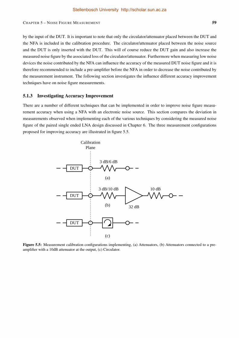
CHAPTER 5 – NOISE FIGURE MEASUREMENT 59
by the input of the DUT. It is important to note that only the circulator/attenuator placed between the DUT and
the NFA is included in the calibration procedure. The circulator/attenuator placed between the noise source
and the DUT is only inserted with the DUT. This will of course reduce the DUT gain and also increase the
measured noise figure by the associated loss of the circulator/attenuator. Furthermore when measuring low noise
devices the noise contributed by the NFA can influence the accuracy of the measured DUT noise figure and it is
therefore recommended to include a pre-amplifier before the NFA in order to decrease the noise contributed by
the measurement instrument. The following section investigates the influence different accuracy improvement
techniques have on noise figure measurements.
5.1.3 Investigating Accuracy Improvement
There are a number of different techniques that can be implemented in order to improve noise figure measu-
rement accuracy when using a NFA with an electronic noise source. This section compares the deviation in
measurements observed when implementing each of the various techniques by considering the measured noise
figure of the paired single ended LNA design discussed in Chapter 6. The three measurement configurations
proposed for improving accuracy are illustrated in figure 5.5.
DUT
32 dB
10 dB3 dB/10 dBDUT
3 dB/6 dBDUT
Calibration Plane
(a)
(b)
(c)
Figure 5.5: Measurement calibration configurations implementing, (a) Attenuators, (b) Attenuators connected to a pre-amplifier with a 10dB attenuator at the output, (c) Circulator.
Stellenbosch University http://scholar.sun.ac.za
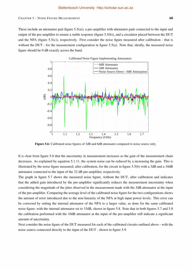
CHAPTER 5 – NOISE FIGURE MEASUREMENT 60
These include an attenuator pad (figure 5.5(a)), a pre-amplifier with attenuator pads connected to the input and
output of the pre-amplifier to ensure a stable response (figure 5.5(b)), and a circulator placed between the DUT
and the NFA (figure 5.5(c)), respectively. First consider the noise figure measured after calibration - that is
without the DUT - for the measurement configuration in figure 5.5(a). Note that, ideally, the measured noise
figure should be 0 dB exactly across the band.
1 1.1 1.2 1.3 1.4 1.5 1.6 1.7-1
-0.8
-0.6
-0.4
-0.2
0
0.2
0.4
0.6
0.8
1Calibrated Noise Figure Implementing Attenuators
Frequency (GHz)
(dB
)
6dB Attenuator3dB AttenuatorNoise Source Direct - 0dB Attenuation
Figure 5.6: Calibrated noise figures of 3dB and 6dB attenuator compared to noise source only.
It is clear from figure 5.6 that the uncertainty in measurement increases as the gain of the measurement chain
decreases. As explained by equation 5.1.11, the system noise can be reduced by a increasing the gain. This is
illustrated by the noise figure measured, after calibration, for the circuit in figure 5.5(b) with a 3dB and a 10dB
attenuator connected to the input of the 32 dB pre-amplifier, respectively.
The graph in figure 5.7 shows the measured noise figure, without the DUT, after calibration and indicates
that the added gain introduced by the pre-amplifier significantly reduces the measurement uncertainty when
considering the magnitude of the jitter observed in the measurement made with the 3dB attenuator at the input
of the pre-amplifier. Comparing the average level of the calibrated noise figure for the two configurations shows
the amount of error introduced due to the non-linearity of the NFA at high input power levels. This error can
be corrected by setting the internal attenuator of the NFA to a larger value, as done for the same calibrated
noise figure, with the internal attenuator set to 15dB, shown in figure 5.8. Note that in both figures 5.7 and 5.8
the calibration performed with the 10dB attenuator at the input of the pre-amplifier still indicate a significant
amount of uncertainty.
Next consider the noise figure of the DUT measured for each of the calibrated circuits outlined above - with the
noise source connected directly to the input of the DUT - shown in figure 5.9.
Stellenbosch University http://scholar.sun.ac.za
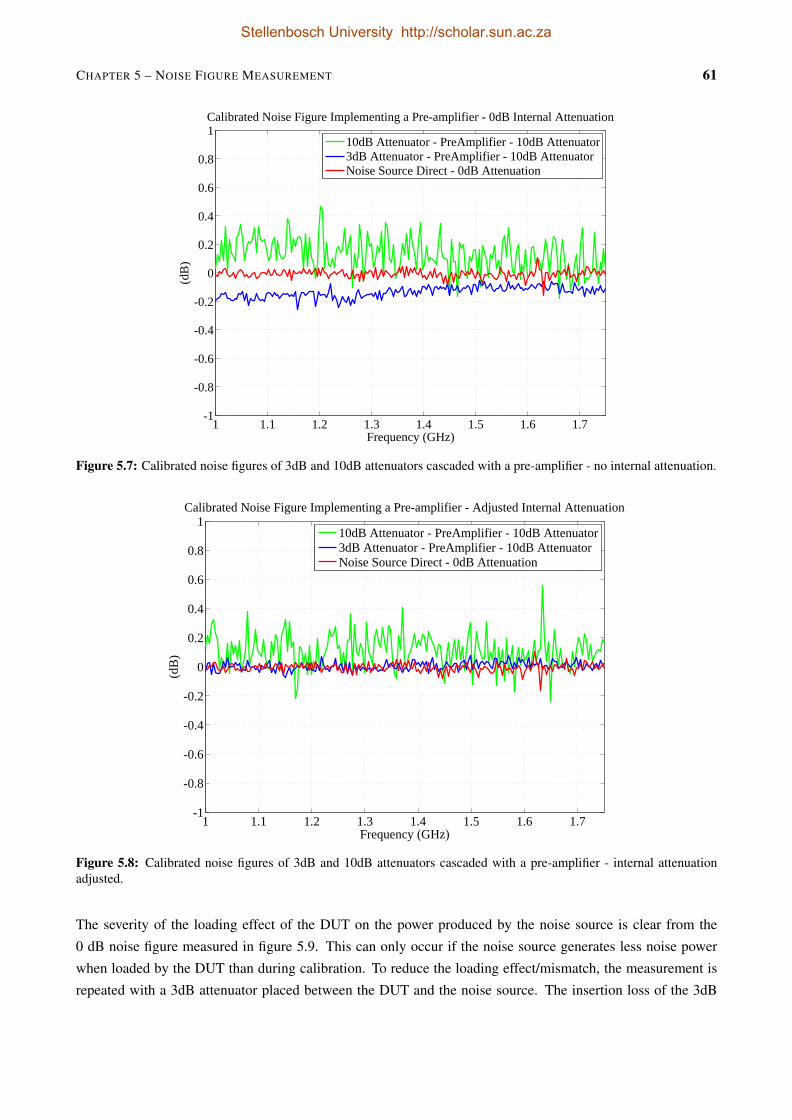
CHAPTER 5 – NOISE FIGURE MEASUREMENT 61
1 1.1 1.2 1.3 1.4 1.5 1.6 1.7-1
-0.8
-0.6
-0.4
-0.2
0
0.2
0.4
0.6
0.8
1Calibrated Noise Figure Implementing a Pre-amplifier - 0dB Internal Attenuation
Frequency (GHz)
(dB
)
10dB Attenuator - PreAmplifier - 10dB Attenuator3dB Attenuator - PreAmplifier - 10dB AttenuatorNoise Source Direct - 0dB Attenuation
Figure 5.7: Calibrated noise figures of 3dB and 10dB attenuators cascaded with a pre-amplifier - no internal attenuation.
1 1.1 1.2 1.3 1.4 1.5 1.6 1.7-1
-0.8
-0.6
-0.4
-0.2
0
0.2
0.4
0.6
0.8
1Calibrated Noise Figure Implementing a Pre-amplifier - Adjusted Internal Attenuation
Frequency (GHz)
(dB
)
10dB Attenuator - PreAmplifier - 10dB Attenuator3dB Attenuator - PreAmplifier - 10dB AttenuatorNoise Source Direct - 0dB Attenuation
Figure 5.8: Calibrated noise figures of 3dB and 10dB attenuators cascaded with a pre-amplifier - internal attenuationadjusted.
The severity of the loading effect of the DUT on the power produced by the noise source is clear from the
0 dB noise figure measured in figure 5.9. This can only occur if the noise source generates less noise power
when loaded by the DUT than during calibration. To reduce the loading effect/mismatch, the measurement is
repeated with a 3dB attenuator placed between the DUT and the noise source. The insertion loss of the 3dB
Stellenbosch University http://scholar.sun.ac.za
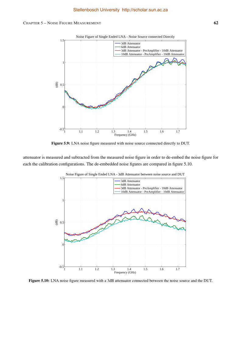
CHAPTER 5 – NOISE FIGURE MEASUREMENT 62
1 1.1 1.2 1.3 1.4 1.5 1.6 1.7-0.5
0
0.5
1
1.5Noise Figure of Single Ended LNA - Noise Source connected Directly
Frequency (GHz)
(dB
)
3dB Attenuator6dB Attenuator3dB Attenuator - PreAmplifier - 10dB Attenuator10dB Attenuator - PreAmplifier - 10dB Attenuator
Figure 5.9: LNA noise figure measured with noise source connected directly to DUT.
attenuator is measured and subtracted from the measured noise figure in order to de-embed the noise figure for
each the calibration configurations. The de-embedded noise figures are compared in figure 5.10.
1 1.1 1.2 1.3 1.4 1.5 1.6 1.7-0.5
0
0.5
1
1.5Noise Figure of Single Ended LNA - 3dB Attenuator between noise source and DUT
Frequency (GHz)
(dB
)
3dB Attenuator6dB Attenuator3dB Attenuator - PreAmplifier - 10dB Attenuator10dB Attenuator - PreAmplifier - 10dB Attenuator
Figure 5.10: LNA noise figure measured with a 3dB attenuator connected between the noise source and the DUT.
Stellenbosch University http://scholar.sun.ac.za

CHAPTER 5 – NOISE FIGURE MEASUREMENT 63
1 1.1 1.2 1.3 1.4 1.5 1.6 1.7-1
-0.8
-0.6
-0.4
-0.2
0
0.2
0.4
0.6
0.8
1Calibrated Noise Figure measured with Circulator
Frequency (GHz)
(dB
)
CirculatorNoise Source
Figure 5.11: Calibrated noise figure with circulator compared to noise source only.
The graph in figure 5.10 shows the effect the large jitter observed in the calibrated noise figure of the calibrations
performed with the 6dB and 10dB attenuators when considering the deviation from the noise figure measured
with the 3dB attenuators. Still the noise figure measured with the 3dB attenuators at the output does not conform
to the simulated noise figure illustrated in figure 6.48. From the discussion outlined in this section it can be
deduced that, in order to perform accurate measurements using a high ENR (15dB) noise source the DUT has
to be well matched to both the noise source and the NFA, using a component with a low insertion loss. This can
be seen when considering the noise figure of the circuit in figure 5.5(c), measured after calibration - without
the DUT, shown in the graph in figure 5.11. The measured insertion loss and reflection coefficients of the
circulators are shown in figure 5.12, indicating that the operating band of the circulator used for the calibration
depicted in figure 5.11 is approximately 1.2-1.4 GHz.
1000 1100 1200 1300 1400 1500 1600 1700-10
-8
-6
-4
-2
0Insertion Loss of Circulator
Frequency (MHz)
(dB
)
|S21|
1000 1100 1200 1300 1400 1500 1600 1700-45
-40
-35
-30
-25
-20
-15
-10
-5
0Isolation and Reflection Coefficients of Circulator
Frequency (MHz)
(dB
)
|S12||S11||S22|
(a) (b)
Figure 5.12: Measured (a) insertion loss and (b) reflection coefficients of the circulator used during calibration.
Stellenbosch University http://scholar.sun.ac.za
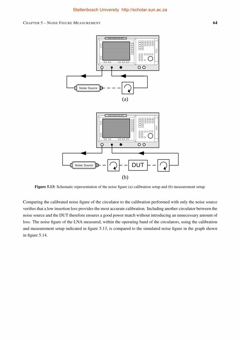
CHAPTER 5 – NOISE FIGURE MEASUREMENT 64
(a)
(b)
NOISE FIGURE ANALYSER
Noise Source
NOISE FIGURE ANALYSER
Noise Source DUT
Figure 5.13: Schematic representation of the noise figure (a) calibration setup and (b) measurement setup.
Comparing the calibrated noise figure of the circulator to the calibration performed with only the noise source
verifies that a low insertion loss provides the most accurate calibration. Including another circulator between the
noise source and the DUT therefore ensures a good power match without introducing an unnecessary amount of
loss. The noise figure of the LNA measured, within the operating band of the circulators, using the calibration
and measurement setup indicated in figure 5.13, is compared to the simulated noise figure in the graph shown
in figure 5.14.
Stellenbosch University http://scholar.sun.ac.za
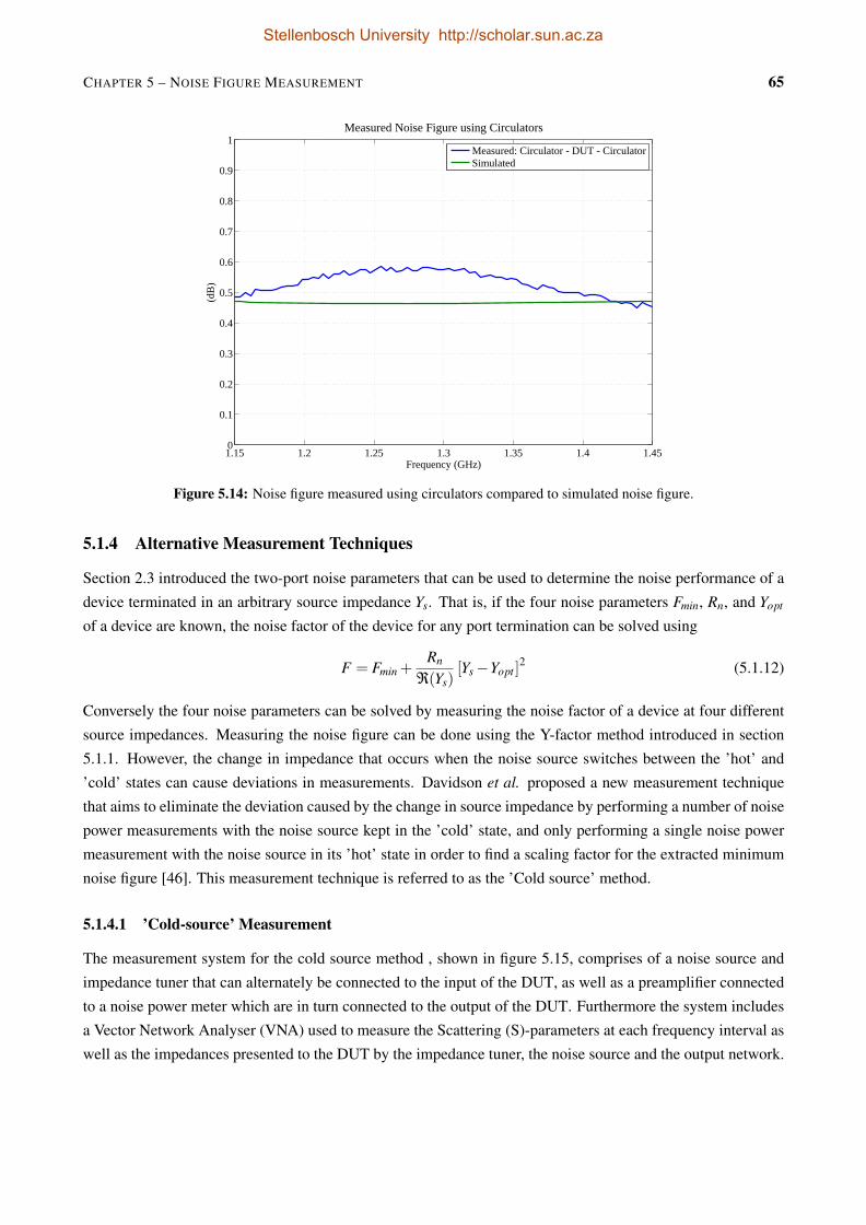
CHAPTER 5 – NOISE FIGURE MEASUREMENT 65
1.15 1.2 1.25 1.3 1.35 1.4 1.450
0.1
0.2
0.3
0.4
0.5
0.6
0.7
0.8
0.9
1Measured Noise Figure using Circulators
Frequency (GHz)
(dB
)
Measured: Circulator - DUT - CirculatorSimulated
Figure 5.14: Noise figure measured using circulators compared to simulated noise figure.
5.1.4 Alternative Measurement Techniques
Section 2.3 introduced the two-port noise parameters that can be used to determine the noise performance of a
device terminated in an arbitrary source impedance Ys. That is, if the four noise parameters Fmin, Rn, and Yopt
of a device are known, the noise factor of the device for any port termination can be solved using
F = Fmin +Rn
ℜ(Ys)[Ys−Yopt ]
2 (5.1.12)
Conversely the four noise parameters can be solved by measuring the noise factor of a device at four different
source impedances. Measuring the noise figure can be done using the Y-factor method introduced in section
5.1.1. However, the change in impedance that occurs when the noise source switches between the ’hot’ and
’cold’ states can cause deviations in measurements. Davidson et al. proposed a new measurement technique
that aims to eliminate the deviation caused by the change in source impedance by performing a number of noise
power measurements with the noise source kept in the ’cold’ state, and only performing a single noise power
measurement with the noise source in its ’hot’ state in order to find a scaling factor for the extracted minimum
noise figure [46]. This measurement technique is referred to as the ’Cold source’ method.
5.1.4.1 ’Cold-source’ Measurement
The measurement system for the cold source method , shown in figure 5.15, comprises of a noise source and
impedance tuner that can alternately be connected to the input of the DUT, as well as a preamplifier connected
to a noise power meter which are in turn connected to the output of the DUT. Furthermore the system includes
a Vector Network Analyser (VNA) used to measure the Scattering (S)-parameters at each frequency interval as
well as the impedances presented to the DUT by the impedance tuner, the noise source and the output network.
Stellenbosch University http://scholar.sun.ac.za
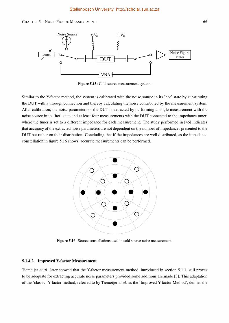
CHAPTER 5 – NOISE FIGURE MEASUREMENT 66
DUTNoise Figure
Meter
VNA
Tuner
Vgs VgdNoise Source
Figure 5.15: Cold source measurement system.
Similar to the Y-factor method, the system is calibrated with the noise source in its ’hot’ state by substituting
the DUT with a through connection and thereby calculating the noise contributed by the measurement system.
After calibration, the noise parameters of the DUT is extracted by performing a single measurement with the
noise source in its ’hot’ state and at least four measurements with the DUT connected to the impedance tuner,
where the tuner is set to a different impedance for each measurement. The study performed in [46] indicates
that accuracy of the extracted noise parameters are not dependent on the number of impedances presented to the
DUT but rather on their distribution. Concluding that if the impedances are well distributed, as the impedance
constellation in figure 5.16 shows, accurate measurements can be performed.
Figure 5.16: Source constellations used in cold source noise measurement.
5.1.4.2 Improved Y-factor Measurement
Tiemeijer et al. later showed that the Y-factor measurement method, introduced in section 5.1.1, still proves
to be adequate for extracting accurate noise parameters provided some additions are made [3]. This adaptation
of the ’classic’ Y-factor method, referred to by Tiemeijer et al. as the ’Improved Y-factor Method’, defines the
Stellenbosch University http://scholar.sun.ac.za
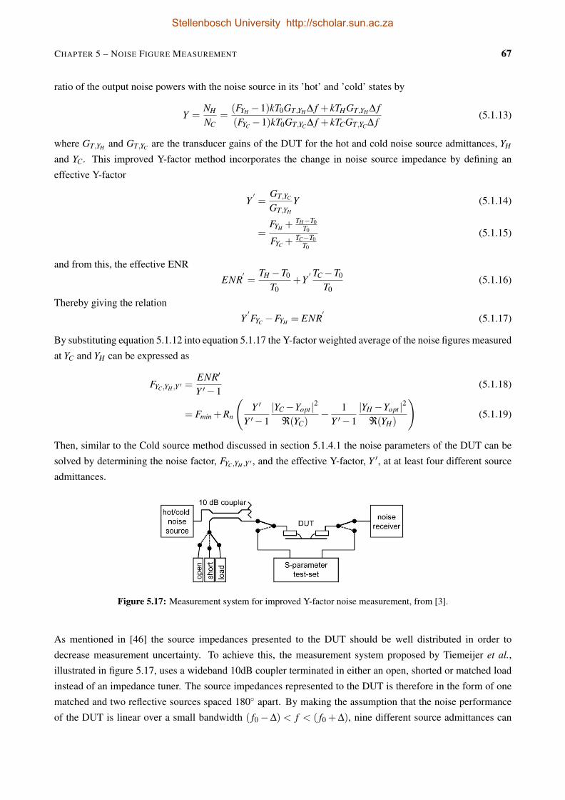
CHAPTER 5 – NOISE FIGURE MEASUREMENT 67
ratio of the output noise powers with the noise source in its ’hot’ and ’cold’ states by
Y =NH
NC=
(FYH −1)kT0GT,YH ∆ f + kTHGT,YH ∆ f(FYC −1)kT0GT,YC ∆ f + kTCGT,YC ∆ f
(5.1.13)
where GT,YH and GT,YC are the transducer gains of the DUT for the hot and cold noise source admittances, YH
and YC. This improved Y-factor method incorporates the change in noise source impedance by defining an
effective Y-factor
Y′=
GT,YC
GT,YH
Y (5.1.14)
=FYH + TH−T0
T0
FYC +TC−T0
T0
(5.1.15)
and from this, the effective ENR
ENR′=
TH −T0
T0+Y
′ TC−T0
T0(5.1.16)
Thereby giving the relation
Y′FYC −FYH = ENR
′(5.1.17)
By substituting equation 5.1.12 into equation 5.1.17 the Y-factor weighted average of the noise figures measured
at YC and YH can be expressed as
FYC,YH ,Y ′ =ENR′
Y ′−1(5.1.18)
= Fmin +Rn
(Y ′
Y ′−1|YC−Yopt |2
ℜ(YC)− 1
Y ′−1|YH −Yopt |2
ℜ(YH)
)(5.1.19)
Then, similar to the Cold source method discussed in section 5.1.4.1 the noise parameters of the DUT can be
solved by determining the noise factor, FYC,YH ,Y ′ , and the effective Y-factor, Y ′, at at least four different source
admittances.
Figure 5.17: Measurement system for improved Y-factor noise measurement, from [3].
As mentioned in [46] the source impedances presented to the DUT should be well distributed in order to
decrease measurement uncertainty. To achieve this, the measurement system proposed by Tiemeijer et al.,
illustrated in figure 5.17, uses a wideband 10dB coupler terminated in either an open, shorted or matched load
instead of an impedance tuner. The source impedances represented to the DUT is therefore in the form of one
matched and two reflective sources spaced 180 apart. By making the assumption that the noise performance
of the DUT is linear over a small bandwidth ( f0−∆) < f < ( f0 +∆), nine different source admittances can
Stellenbosch University http://scholar.sun.ac.za
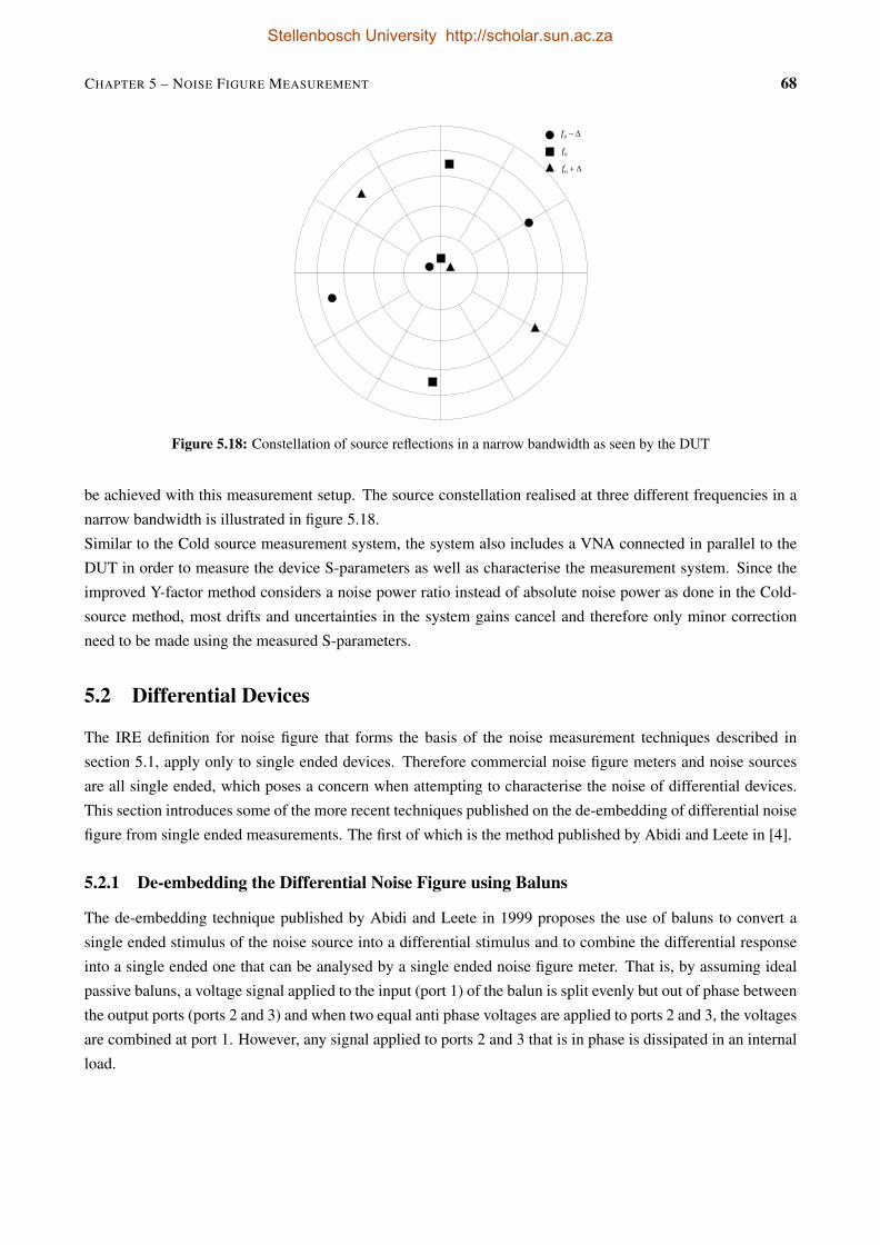
CHAPTER 5 – NOISE FIGURE MEASUREMENT 68
0f
0f
0f
Figure 5.18: Constellation of source reflections in a narrow bandwidth as seen by the DUT
be achieved with this measurement setup. The source constellation realised at three different frequencies in a
narrow bandwidth is illustrated in figure 5.18.
Similar to the Cold source measurement system, the system also includes a VNA connected in parallel to the
DUT in order to measure the device S-parameters as well as characterise the measurement system. Since the
improved Y-factor method considers a noise power ratio instead of absolute noise power as done in the Cold-
source method, most drifts and uncertainties in the system gains cancel and therefore only minor correction
need to be made using the measured S-parameters.
5.2 Differential Devices
The IRE definition for noise figure that forms the basis of the noise measurement techniques described in
section 5.1, apply only to single ended devices. Therefore commercial noise figure meters and noise sources
are all single ended, which poses a concern when attempting to characterise the noise of differential devices.
This section introduces some of the more recent techniques published on the de-embedding of differential noise
figure from single ended measurements. The first of which is the method published by Abidi and Leete in [4].
5.2.1 De-embedding the Differential Noise Figure using Baluns
The de-embedding technique published by Abidi and Leete in 1999 proposes the use of baluns to convert a
single ended stimulus of the noise source into a differential stimulus and to combine the differential response
into a single ended one that can be analysed by a single ended noise figure meter. That is, by assuming ideal
passive baluns, a voltage signal applied to the input (port 1) of the balun is split evenly but out of phase between
the output ports (ports 2 and 3) and when two equal anti phase voltages are applied to ports 2 and 3, the voltages
are combined at port 1. However, any signal applied to ports 2 and 3 that is in phase is dissipated in an internal
load.
Stellenbosch University http://scholar.sun.ac.za
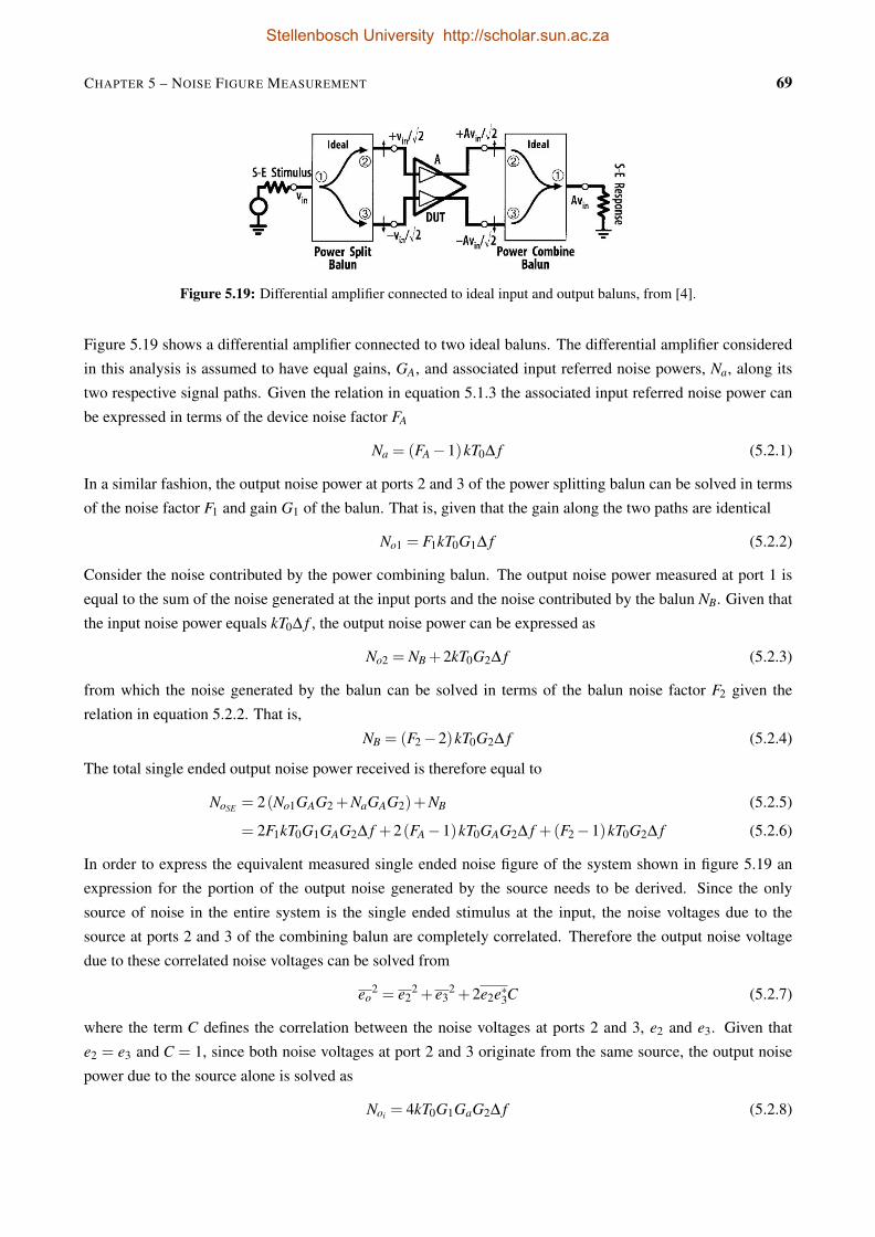
CHAPTER 5 – NOISE FIGURE MEASUREMENT 69
Figure 5.19: Differential amplifier connected to ideal input and output baluns, from [4].
Figure 5.19 shows a differential amplifier connected to two ideal baluns. The differential amplifier considered
in this analysis is assumed to have equal gains, GA, and associated input referred noise powers, Na, along its
two respective signal paths. Given the relation in equation 5.1.3 the associated input referred noise power can
be expressed in terms of the device noise factor FA
Na = (FA−1)kT0∆ f (5.2.1)
In a similar fashion, the output noise power at ports 2 and 3 of the power splitting balun can be solved in terms
of the noise factor F1 and gain G1 of the balun. That is, given that the gain along the two paths are identical
No1 = F1kT0G1∆ f (5.2.2)
Consider the noise contributed by the power combining balun. The output noise power measured at port 1 is
equal to the sum of the noise generated at the input ports and the noise contributed by the balun NB. Given that
the input noise power equals kT0∆ f , the output noise power can be expressed as
No2 = NB +2kT0G2∆ f (5.2.3)
from which the noise generated by the balun can be solved in terms of the balun noise factor F2 given the
relation in equation 5.2.2. That is,
NB = (F2−2)kT0G2∆ f (5.2.4)
The total single ended output noise power received is therefore equal to
NoSE = 2(No1GAG2 +NaGAG2)+NB (5.2.5)
= 2F1kT0G1GAG2∆ f +2(FA−1)kT0GAG2∆ f +(F2−1)kT0G2∆ f (5.2.6)
In order to express the equivalent measured single ended noise figure of the system shown in figure 5.19 an
expression for the portion of the output noise generated by the source needs to be derived. Since the only
source of noise in the entire system is the single ended stimulus at the input, the noise voltages due to the
source at ports 2 and 3 of the combining balun are completely correlated. Therefore the output noise voltage
due to these correlated noise voltages can be solved from
eo2 = e2
2 + e32 +2e2e∗3C (5.2.7)
where the term C defines the correlation between the noise voltages at ports 2 and 3, e2 and e3. Given that
e2 = e3 and C = 1, since both noise voltages at port 2 and 3 originate from the same source, the output noise
power due to the source alone is solved as
Noi = 4kT0G1GaG2∆ f (5.2.8)
Stellenbosch University http://scholar.sun.ac.za
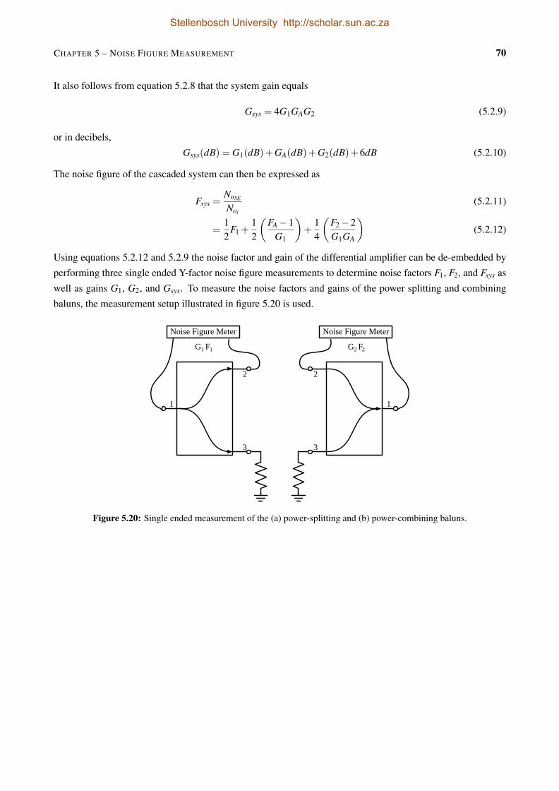
CHAPTER 5 – NOISE FIGURE MEASUREMENT 70
It also follows from equation 5.2.8 that the system gain equals
Gsys = 4G1GAG2 (5.2.9)
or in decibels,
Gsys(dB) = G1(dB)+GA(dB)+G2(dB)+6dB (5.2.10)
The noise figure of the cascaded system can then be expressed as
Fsys =NoSE
Noi
(5.2.11)
=12
F1 +12
(FA−1
G1
)+
14
(F2−2G1GA
)(5.2.12)
Using equations 5.2.12 and 5.2.9 the noise factor and gain of the differential amplifier can be de-embedded by
performing three single ended Y-factor noise figure measurements to determine noise factors F1, F2, and Fsys as
well as gains G1, G2, and Gsys. To measure the noise factors and gains of the power splitting and combining
baluns, the measurement setup illustrated in figure 5.20 is used.
1
2
3
Noise Figure Meter
1
2
3
Noise Figure Meter
G F G F11 2 2
Figure 5.20: Single ended measurement of the (a) power-splitting and (b) power-combining baluns.
Stellenbosch University http://scholar.sun.ac.za

CHAPTER 5 – NOISE FIGURE MEASUREMENT 71
By assuming ideal operation, the balun noise figure and gain can be measured by terminating the open port in
a matched load. Furthermore, it can be shown that for any matched passive two-port network the noise factor
equals the reciprocal of the insertion loss of the network. Thus, for an ideal balun, the single ended insertion loss
G = 1/2 and therefore the noise factor F = 1/G = 2. It then follows from equation 5.2.12 that, for F1 = F2 = 2
and G1 = G2 = 1/2,
Fsys = FA (5.2.13)
and similarly
Gsys = GA (5.2.14)
thereby validating the use of equation 5.2.12 for the de-embedding of the noise figure of a differential amplifier
using baluns.
5.2.2 Deriving the Mixed-Mode Noise Correlation Matrix from Noise Figure Measurements
The noise analysis published by Abidi and Leete, described in section 5.2.1, assumes no correlation between
the equivalent output noise sources of the differential amplifier and also only defines the differential noise
performance of the DUT within the measurement system. A similar measurement system, incorporating baluns,
can be used to obtain the noise correlation matrix of a four-port differential device. Then by using the theory on
the noise correlation matrix described in Chapter 3, the derived noise correlation matrix can be used to obtain
the noise parameters of the DUT from which the noise performance can be solved for any input termination.
This measurement procedure was first published by Tiemeijer et al. in [5]. The proposed technique considers
the impedance representation of a linear noisy four port network, as illustrated in figure 5.21.
Figure 5.21: Impedance representation of a noisy four-port network, from [5].
Using the improved Y-factor method, the 2x2 sub-matrix CZ13 can be solved by performing a single ended
measurement using ports 1 and 3, with ports 2 and 4 left open ended. The sub-matrix CZ13 is given by
CZ13 =
[CZ.11 CZ.13
CZ.31 CZ.33
](5.2.15)
Solving the noise parameters using the improved Y-factor method, discussed in section 5.1.4.2, the chain repre-
sentation of the noise correlation matrix can be obtained and transformed to the equivalent impedance repre-
sentation using the theory on the noise correlation matrix discussed in Chapter 3.
Stellenbosch University http://scholar.sun.ac.za
CHAPTER 5 – NOISE FIGURE MEASUREMENT 72
The other elements of the 16 element impedance correlation matrix can be obtained by repeating this mea-
surement, however this can become a tedious task and leads to multiple values for the diagonal terms of the
correlation matrix. The technique proposed by Tiemeijer et al. uses the theory on the mixed-mode noise cor-
relation matrix, derived in section 6.2.1, to simplify this measurement procedure by first of all assuming that
the network is sufficiently symmetrical such that the single ended noise correlation matrix CZ13 equals CZ24 -
the noise correlation matrix obtained by performing a single ended noise measurement using ports 2 and 4 with
ports 1 and 3 left open ended. Also due to symmetry the cross-mode elements of the mixed-mode correlation
can be neglected. Resulting in the mixed-mode noise correlation matrix in equation 5.2.16
CZMM =
CZMM.11 CZMM.12 0 0
CZMM.21 CZMM.22 0 0
0 0 CZMM.33 CZMM.34
0 0 CZMM.43 CZMM.44
(5.2.16)
where subscripts MM.1 and MM.2 denote differential signals at the input and output, and MM.3 and MM.4
denote common-mode signals at the input and output, respectively. The mixed mode noise correlation matrix
can therefore be derived by performing one differential and one common-mode noise measurement. Due to
the fact that differential amplifiers exhibit high common mode rejection, the common-mode noise figure can
prove difficult to measure. Therefore Tiemeijer et al. proposed the de-embedding of the remaining terms of the
4x4 impedance correlation matrix by performing one single ended noise measurement to obtain CZ13 and one
differential noise measurement to obtain the differential sub-matrix
CZdd =
[CZMM.11 CZMM.12
CZMM.21 CZMM.22
](5.2.17)
Similar to the differential noise figure measurement system of Abidi and Leete outlined in section 5.2.1, Tie-
meijer et al. also suggests the use of baluns to measure the differential noise performance of the differential
DUT where, instead of only measuring the differential noise factor of the device, the differential noise para-
meters of the device are determined by using the improved Y-factor method instead of the classical Y-factor
method employed by Abidi and Leete.
The mixed mode differential sub-matrix CZdd can then readily be solved from the extracted differential noise
parameters. Recalling the mixed-mode impedance correlation matrix is determined using a relation analagous
to that given in equation 6.2.19 the elements of the differential sub-matrix defined in equation 5.2.17 can be
expressed in terms of the elements of the 4x4 impedance correlation matrix. That is,
CZMM.11 =CZ.11−CZ.12−CZ.21 +CZ.22 (5.2.18)
CZMM.12 =CZ.13−CZ.14−CZ.23 +CZ.24 (5.2.19)
CZMM.21 =CZ.31−CZ.32−CZ.41 +CZ.42 (5.2.20)
CZMM.22 =CZ.33−CZ.34−CZ.43 +CZ.44 (5.2.21)
Stellenbosch University http://scholar.sun.ac.za

CHAPTER 5 – NOISE FIGURE MEASUREMENT 73
Then using the assumption that CZ13 =CZ24 due to symmetry, the remaining cross-correlation coefficients can
be solved in terms of the elements of CZ13 and CZdd giving
CZ.12 =CZ.21 =12(CZ.11 +CZ.22−CZMM.11) (5.2.22)
CZ.14 =CZ.23 =12(CZ.13 +CZ.24−CZMM.12) (5.2.23)
CZ.32 =CZ.41 =12(CZ.31 +CZ.42−CZMM.21) (5.2.24)
CZ.34 =CZ.43 =12(CZ.33 +CZ.44−CZMM.22) (5.2.25)
In this way the full 4x4 impedance noise correlation matrix, from which the noise performance of the linear
four-port network can be predicted in any port termination, is solved.
5.2.3 De-embedding the Differential Noise Figure without the use of Baluns
Although the use of baluns or hybrids simplifies the measurement procedure, proper de-embedding of the
baluns/hybrids can prove to be a difficult task. Furthermore the baluns and hybrids used in the measurements
might limit the frequency range of the measurement and wideband measurements may therefore require more
than one set of baluns or hybrids during measurement. Belostotski proposed a technique through which the
differential noise figure of a four-port network can be de-embedded by performing single ended measurements
between two ports with the unused ports terminated in matched loads [47]. Similar to the technique proposed
by Abidi and Leete, Belostotski’s measurement procedure only de-embeds the differential noise figure of the
device. In this respect, the method proposed by Tiemeijer et al. proves more advantageous as it provides the full
differential noise parameters of the device, making it possible to characterise the differential noise performance
of the device in any arbitrary port termination. However, due to the fact that the differential LNA design
considered in the scope of this text comprises of an output 180-hybrid coupler, the measurement techniques
discussed in sections 5.2.1 and 5.2.2 can not be applied to this design since both procedures incorporate an
output balun that requires de-embedding to obtain the differential noise performance. Therefore, Belostotski’s
technique, published in [47], is applied in this section to derive an expression for the differential noise figure of
a differential LNA in terms of the noise figures of two single-ended measurements.
Stellenbosch University http://scholar.sun.ac.za
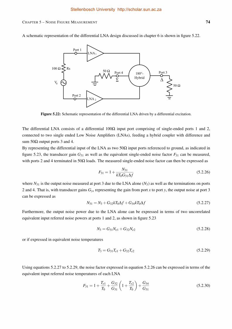
CHAPTER 5 – NOISE FIGURE MEASUREMENT 74
A schematic representation of the differential LNA design discussed in chapter 6 is shown in figure 5.22.
180°-Hybrid
100 Ω
LNA 1
Vd
50 Ω
50 Ω
ΔΣ
LNA 2
Port 1
Port 2
Port 4 Port 3Rs
Figure 5.22: Schematic representation of the differential LNA driven by a differential excitation.
The differential LNA consists of a differential 100Ω input port comprising of single-ended ports 1 and 2,
connected to two single ended Low Noise Amplifiers (LNAs), feeding a hybrid coupler with difference and
sum 50Ω output ports 3 and 4.
By representing the differential input of the LNA as two 50Ω input ports referenced to ground, as indicated in
figure 5.23, the transducer gain G31 as well as the equivalent single-ended noise factor F31 can be measured,
with ports 2 and 4 terminated in 50Ω loads. The measured single-ended noise factor can then be expressed as
F31 = 1+N31
kT0G31∆ f(5.2.26)
where N31 is the output noise measured at port 3 due to the LNA alone (N3) as well as the terminations on ports
2 and 4. That is, with transducer gains Gyx representing the gain from port x to port y, the output noise at port 3
can be expressed as
N31 = N3 +G32kT0∆ f +G34kT0∆ f (5.2.27)
Furthermore, the output noise power due to the LNA alone can be expressed in terms of two uncorrelated
equivalent input referred noise powers at ports 1 and 2, as shown in figure 5.23
N3 = G31Ne1 +G32Ne2 (5.2.28)
or if expressed in equivalent noise temperatures
T3 = G31Te1 +G32Te2 (5.2.29)
Using equations 5.2.27 to 5.2.29, the noise factor expressed in equation 5.2.26 can be expressed in terms of the
equivalent input referred noise temperatures of each LNA
F31 = 1+Te1
T0+
G32
G31
(1+
Te2
T0
)+
G34
G31(5.2.30)
Stellenbosch University http://scholar.sun.ac.za
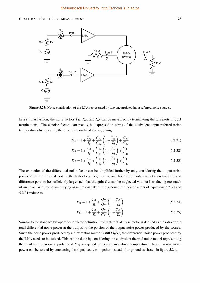
CHAPTER 5 – NOISE FIGURE MEASUREMENT 75
180°-Hybrid
50 Ω
LNA 1
Vd 50 Ω
50 Ω
ΔΣ
LNA 2
Port 1
Port 2
Port 4 Port 3
50 Ω
Vd
Rs
Rs
Ne1
Ne2
Figure 5.23: Noise contribution of the LNA represented by two uncorrelated input referred noise sources.
In a similar fashion, the noise factors F32, F41, and F42 can be measured by terminating the idle ports in 50Ω
terminations. These noise factors can readily be expressed in terms of the equivalent input referred noise
temperatures by repeating the procedure outlined above, giving
F32 = 1+Te2
T0+
G31
G32
(1+
Te1
T0
)+
G34
G32(5.2.31)
F41 = 1+Te1
T0+
G42
G41
(1+
Te2
T0
)+
G43
G41(5.2.32)
F42 = 1+Te2
T0+
G41
G42
(1+
Te1
T0
)+
G43
G42(5.2.33)
The extraction of the differential noise factor can be simplified further by only considering the output noise
power at the differential port of the hybrid coupler, port 3, and taking the isolation between the sum and
difference ports to be sufficiently large such that the gain G34 can be neglected without introducing too much
of an error. With these simplifying assumptions taken into account, the noise factors of equations 5.2.30 and
5.2.31 reduce to
F31 = 1+Te1
T0+
G32
G31
(1+
Te2
T0
)(5.2.34)
F32 = 1+Te2
T0+
G31
G32
(1+
Te1
T0
)(5.2.35)
Similar to the standard two-port noise factor definition, the differential noise factor is defined as the ratio of the
total differential noise power at the output, to the portion of the output noise power produced by the source.
Since the noise power produced by a differential source is still kT0∆ f , the differential noise power produced by
the LNA needs to be solved. This can be done by considering the equivalent thermal noise model representing
the input referred noise at ports 1 and 2 by an equivalent increase in ambient temperature. The differential noise
power can be solved by connecting the signal sources together instead of to ground as shown in figure 5.24.
Stellenbosch University http://scholar.sun.ac.za
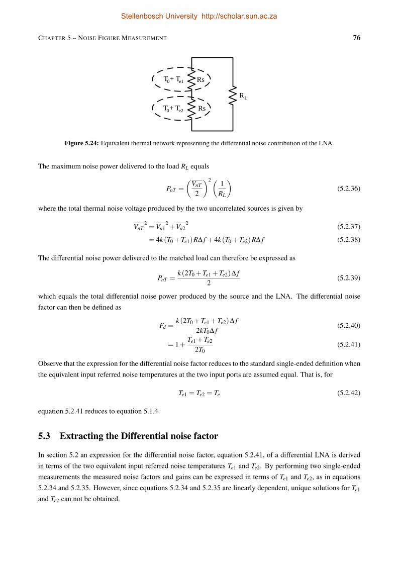
CHAPTER 5 – NOISE FIGURE MEASUREMENT 76
Rs
Rs
RL
T + T0 e1
T + T0 e2
Figure 5.24: Equivalent thermal network representing the differential noise contribution of the LNA.
The maximum noise power delivered to the load RL equals
PnT =
(VnT
2
)2( 1RL
)(5.2.36)
where the total thermal noise voltage produced by the two uncorrelated sources is given by
VnT2=Vn1
2+Vn2
2 (5.2.37)
= 4k (T0 +Te1)R∆ f +4k (T0 +Te2)R∆ f (5.2.38)
The differential noise power delivered to the matched load can therefore be expressed as
PnT =k (2T0 +Te1 +Te2)∆ f
2(5.2.39)
which equals the total differential noise power produced by the source and the LNA. The differential noise
factor can then be defined as
Fd =k (2T0 +Te1 +Te2)∆ f
2kT0∆ f(5.2.40)
= 1+Te1 +Te2
2T0(5.2.41)
Observe that the expression for the differential noise factor reduces to the standard single-ended definition when
the equivalent input referred noise temperatures at the two input ports are assumed equal. That is, for
Te1 = Te2 = Te (5.2.42)
equation 5.2.41 reduces to equation 5.1.4.
5.3 Extracting the Differential noise factor
In section 5.2 an expression for the differential noise factor, equation 5.2.41, of a differential LNA is derived
in terms of the two equivalent input referred noise temperatures Te1 and Te2. By performing two single-ended
measurements the measured noise factors and gains can be expressed in terms of Te1 and Te2, as in equations
5.2.34 and 5.2.35. However, since equations 5.2.34 and 5.2.35 are linearly dependent, unique solutions for Te1
and Te2 can not be obtained.
Stellenbosch University http://scholar.sun.ac.za

CHAPTER 5 – NOISE FIGURE MEASUREMENT 77
Therefore the noise power at port 3 due to the LNA alone is solved in terms of the measured noise factors (F31
and F32) and respective gains (G31 and G32). That is, by substituting equation 5.2.27 into equation 5.2.26, the
output noise power due to the LNA alone, is solved to be equal to
N3 = kT0 [(F31−1)G31−G32] (5.3.1)
and, in a similar fashion it can be shown that
N3 = kT0 [(F32−1)G32−G31] (5.3.2)
To reduce measurement uncertainties, N3 is defined as the average of equations 5.3.1 and 5.3.2 such that
N3 =kT0
2[(F32−2)G31 +(F32−2)G32] (5.3.3)
By comparing equation 5.3.3 to equation 5.2.28 the equivalent input referred noise temperatures can be expres-
sed in terms of F31 and F32
Te1 = (F31−2)T0
2(5.3.4)
Te2 = (F32−2)T0
2(5.3.5)
The differential noise factor can therefore be solved from the two single ended noise factor measurements,
giving the relationship
Fd =F31 +F32
4(5.3.6)
Note that equation 5.3.6 applies only for the ideal scenario when no deviation in gains G31 and G32 can be assu-
med. Considering the fact that measured single ended noise figures F31 and F32 are dependent on the measured
gain it would be useful to define the deviation of the measured differential noise figure due to deviations in gain
measurements. This is done by defining two constants k0 and ∆ in terms of the gain ratios, where
k0 =12
[G32
G31+
G31
G32
](5.3.7)
G32
G31= k0 +∆ (5.3.8)
G31
G32= k0−∆ (5.3.9)
Using equations 5.3.7 to 5.3.9 a new expression for the differential noise figure is derived, taking the effect of
the deviation in the two gains into account. That is,
Fd =(2+∆)F31 +(2−∆)F32
2(k0 +1)2 (5.3.10)
Observe that for equal gains it follows that k0 = 1 and ∆ = 0 and so equation 5.3.10 reduces to equation 5.3.6.
Stellenbosch University http://scholar.sun.ac.za
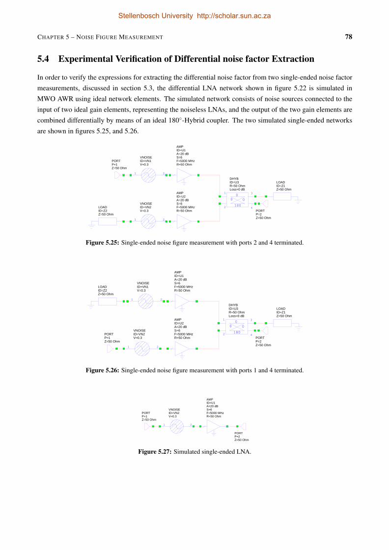
CHAPTER 5 – NOISE FIGURE MEASUREMENT 78
5.4 Experimental Verification of Differential noise factor Extraction
In order to verify the expressions for extracting the differential noise factor from two single-ended noise factor
measurements, discussed in section 5.3, the differential LNA network shown in figure 5.22 is simulated in
MWO AWR using ideal network elements. The simulated network consists of noise sources connected to the
input of two ideal gain elements, representing the noiseless LNAs, and the output of the two gain elements are
combined differentially by means of an ideal 180-Hybrid coupler. The two simulated single-ended networks
are shown in figures 5.25, and 5.26.
AMPID=U1A=20 dBS=6F=5000 MHzR=50 Ohm
180
000
1
2
3
4
DHYBID=U3R=50 OhmLoss=0 dB
LOADID=Z1Z=50 Ohm
AMPID=U2A=20 dBS=6F=5000 MHzR=50 Ohm
1 2
VNOISEID=VN2V=0.3
1 2
VNOISEID=VN1V=0.3
LOADID=Z2Z=50 Ohm
PORTP=1Z=50 Ohm
PORTP=2Z=50 Ohm
Figure 5.25: Single-ended noise figure measurement with ports 2 and 4 terminated.
AMPID=U1A=20 dBS=6F=5000 MHzR=50 Ohm
180
000
1
2
3
4
DHYBID=U3R=50 OhmLoss=0 dB
LOADID=Z1Z=50 Ohm
AMPID=U2A=20 dBS=6F=5000 MHzR=50 Ohm
1 2
VNOISEID=VN2V=0.3
1 2
VNOISEID=VN1V=0.3
LOADID=Z2Z=50 Ohm
PORTP=2Z=50 Ohm
PORTP=1Z=50 Ohm
Figure 5.26: Single-ended noise figure measurement with ports 1 and 4 terminated.
AMPID=U1A=20 dBS=6F=5000 MHzR=50 Ohm
1 2
VNOISEID=VN2V=0.3
PORTP=1Z=50 Ohm
PORTP=2Z=50 Ohm
Figure 5.27: Simulated single-ended LNA.
Stellenbosch University http://scholar.sun.ac.za
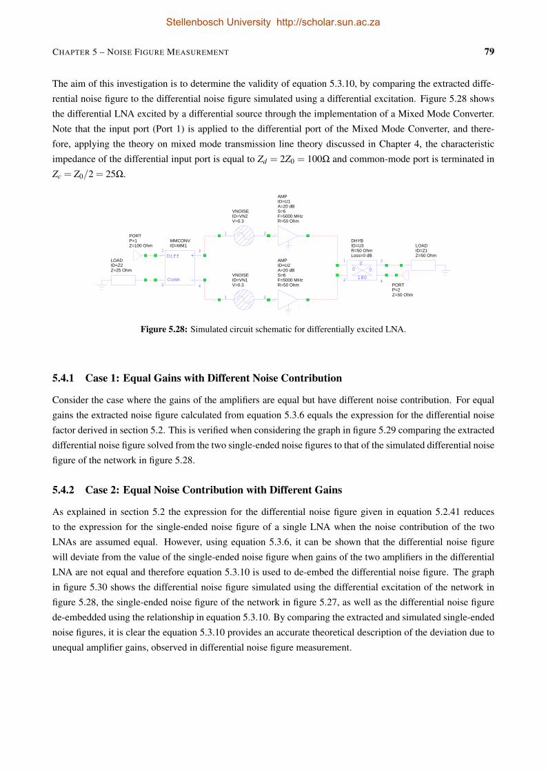
CHAPTER 5 – NOISE FIGURE MEASUREMENT 79
The aim of this investigation is to determine the validity of equation 5.3.10, by comparing the extracted diffe-
rential noise figure to the differential noise figure simulated using a differential excitation. Figure 5.28 shows
the differential LNA excited by a differential source through the implementation of a Mixed Mode Converter.
Note that the input port (Port 1) is applied to the differential port of the Mixed Mode Converter, and there-
fore, applying the theory on mixed mode transmission line theory discussed in Chapter 4, the characteristic
impedance of the differential input port is equal to Zd = 2Z0 = 100Ω and common-mode port is terminated in
Zc = Z0/2 = 25Ω.
AMPID=U1A=20 dBS=6F=5000 MHzR=50 Ohm
180
000
1
2
3
4
DHYBID=U3R=50 OhmLoss=0 dB
LOADID=Z1Z=50 Ohm
AMPID=U2A=20 dBS=6F=5000 MHzR=50 Ohm
Diff
Comm
+
-
1
2
3
4
MMCONVID=MM1
LOADID=Z2Z=25 Ohm
1 2
VNOISEID=VN1V=0.3
1 2
VNOISEID=VN2V=0.3
PORTP=2Z=50 Ohm
PORTP=1Z=100 Ohm
Figure 5.28: Simulated circuit schematic for differentially excited LNA.
5.4.1 Case 1: Equal Gains with Different Noise Contribution
Consider the case where the gains of the amplifiers are equal but have different noise contribution. For equal
gains the extracted noise figure calculated from equation 5.3.6 equals the expression for the differential noise
factor derived in section 5.2. This is verified when considering the graph in figure 5.29 comparing the extracted
differential noise figure solved from the two single-ended noise figures to that of the simulated differential noise
figure of the network in figure 5.28.
5.4.2 Case 2: Equal Noise Contribution with Different Gains
As explained in section 5.2 the expression for the differential noise figure given in equation 5.2.41 reduces
to the expression for the single-ended noise figure of a single LNA when the noise contribution of the two
LNAs are assumed equal. However, using equation 5.3.6, it can be shown that the differential noise figure
will deviate from the value of the single-ended noise figure when gains of the two amplifiers in the differential
LNA are not equal and therefore equation 5.3.10 is used to de-embed the differential noise figure. The graph
in figure 5.30 shows the differential noise figure simulated using the differential excitation of the network in
figure 5.28, the single-ended noise figure of the network in figure 5.27, as well as the differential noise figure
de-embedded using the relationship in equation 5.3.10. By comparing the extracted and simulated single-ended
noise figures, it is clear the equation 5.3.10 provides an accurate theoretical description of the deviation due to
unequal amplifier gains, observed in differential noise figure measurement.
Stellenbosch University http://scholar.sun.ac.za

CHAPTER 5 – NOISE FIGURE MEASUREMENT 80
1000 1100 1200 1300 1400 1500 1600 17000
0.1
0.2
0.3
0.4
0.5
0.6
0.7
0.8
0.9
1De-embedded Differential Noise Figure
Frequency (MHz)
(dB
)
Mixed-Mode Differential Noise FigureDe-emedded Differential Noise Figure
Figure 5.29: Comparing the extracted differential noise figure to the noise figure obtained from a differential excitation.
1000 1100 1200 1300 1400 1500 1600 17000
0.1
0.2
0.3
0.4
0.5
0.6
0.7
0.8
0.9
1De-embedded Differential Noise Figure
Frequency (MHz)
(dB
)
Mixed-Mode Differential Noise FigureSingle ended Noise FigureDe-embedded Differential Noise Figure
Figure 5.30: De-embedded differential noise figure validated.
Stellenbosch University http://scholar.sun.ac.za

CHAPTER 5 – NOISE FIGURE MEASUREMENT 81
5.5 Conclusion
This chapter introduced the theory of the Y-factor noise figure measurement procedure that forms the basis for
the internal operation of most single-ended noise figure measurement instruments. The measurement system
used to measure the results discussed in Chapter 6 was discussed, as well as methods to increase noise figure
measurement accuracy. Then, based on two single-ended measurements an expression for the differential noise
figure was derived and verified using two case studies. The first case study confirmed that the differential noise
figure can be accurately extracted from two single-ended measurements, when the gain curves of the two am-
plifiers are considered equal. Whereas the second case study quantified the deviation from the ideal differential
noise figure caused by a difference in amplifier gains. The differential noise figure extraction described in this
chapter is applied to all the measured results given in Chapter 6.
Stellenbosch University http://scholar.sun.ac.za

Chapter 6
Differential Low Noise Amplifier Design andNoise Figure Verification
This chapter applies the signal and noise characteristics of differential circuits discussed in the preceding chap-
ters to the design of L-band Differential Low Noise Amplifiers (dLNAs). The two main topologies of differen-
tial amplifiers, balanced and differential, are illustrated in figure 6.1, with the predominant difference between
the two topologies being that the differential topology displays inherent common-mode suppression. As men-
tioned in the Introduction, the subsequent receiver blocks after the low noise gain block in the proposed receiver
front end, are all commonly implemented using single ended devices. Therefore, the dLNA implemented in
the low noise gain block needs to convert the balanced antenna output into a single ended output that can be
connected to the remaining receiver chain. A single ended output is generally realised in differential topology
by inserting an active load along the signal path of one of the amplifiers and using the other as an unbalanced
output. The use of active loads can realise high open circuit differential gain, that can decrease severely due to
loading effects and therefore a gain stage with a high input impedance usually precedes the unbalanced output.
(a) (b)
Figure 6.1: Two main topologies of differential amplifiers: (a) Balanced topology (b) and Differential topology.
82
Stellenbosch University http://scholar.sun.ac.za
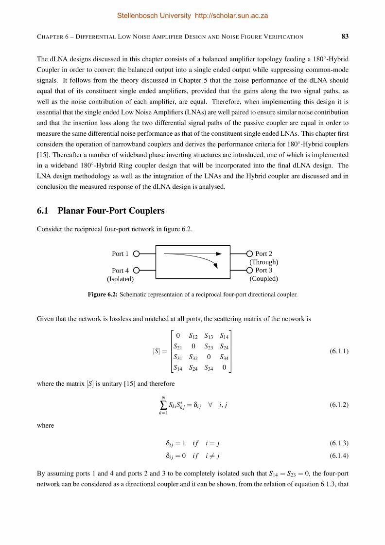
CHAPTER 6 – DIFFERENTIAL LOW NOISE AMPLIFIER DESIGN AND NOISE FIGURE VERIFICATION 83
The dLNA designs discussed in this chapter consists of a balanced amplifier topology feeding a 180-Hybrid
Coupler in order to convert the balanced output into a single ended output while suppressing common-mode
signals. It follows from the theory discussed in Chapter 5 that the noise performance of the dLNA should
equal that of its constituent single ended amplifiers, provided that the gains along the two signal paths, as
well as the noise contribution of each amplifier, are equal. Therefore, when implementing this design it is
essential that the single ended Low Noise Amplifiers (LNAs) are well paired to ensure similar noise contribution
and that the insertion loss along the two differential signal paths of the passive coupler are equal in order to
measure the same differential noise performance as that of the constituent single ended LNAs. This chapter first
considers the operation of narrowband couplers and derives the performance criteria for 180-Hybrid couplers
[15]. Thereafter a number of wideband phase inverting structures are introduced, one of which is implemented
in a wideband 180-Hybrid Ring coupler design that will be incorporated into the final dLNA design. The
LNA design methodology as well as the integration of the LNAs and the Hybrid coupler are discussed and in
conclusion the measured response of the dLNA design is analysed.
6.1 Planar Four-Port Couplers
Consider the reciprocal four-port network in figure 6.2.
Port 1 Port 2(Through)
Port 3(Coupled)
Port 4(Isolated)
Figure 6.2: Schematic representaion of a reciprocal four-port directional coupler.
Given that the network is lossless and matched at all ports, the scattering matrix of the network is
[S] =
0 S12 S13 S14
S21 0 S23 S24
S31 S32 0 S34
S14 S24 S34 0
(6.1.1)
where the matrix [S] is unitary [15] and therefore
N
∑k=1
SkiS∗k j = δi j ∀ i, j (6.1.2)
where
δi j = 1 i f i = j (6.1.3)
δi j = 0 i f i 6= j (6.1.4)
By assuming ports 1 and 4 and ports 2 and 3 to be completely isolated such that S14 = S23 = 0, the four-port
network can be considered as a directional coupler and it can be shown, from the relation of equation 6.1.3, that
Stellenbosch University http://scholar.sun.ac.za
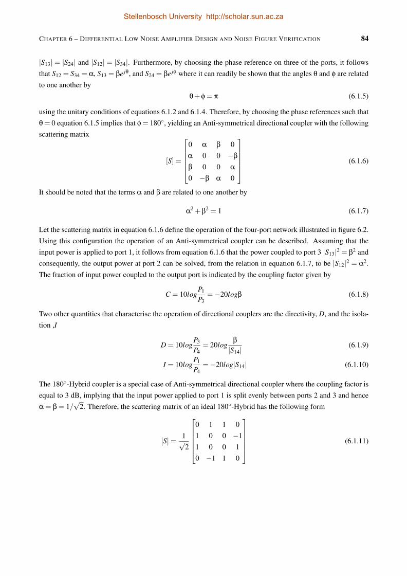
CHAPTER 6 – DIFFERENTIAL LOW NOISE AMPLIFIER DESIGN AND NOISE FIGURE VERIFICATION 84
|S13| = |S24| and |S12| = |S34|. Furthermore, by choosing the phase reference on three of the ports, it follows
that S12 = S34 = α, S13 = βe jθ, and S24 = βe jφ where it can readily be shown that the angles θ and φ are related
to one another by
θ+φ = π (6.1.5)
using the unitary conditions of equations 6.1.2 and 6.1.4. Therefore, by choosing the phase references such that
θ = 0 equation 6.1.5 implies that φ = 180, yielding an Anti-symmetrical directional coupler with the following
scattering matrix
[S] =
0 α β 0
α 0 0 −β
β 0 0 α
0 −β α 0
(6.1.6)
It should be noted that the terms α and β are related to one another by
α2 +β
2 = 1 (6.1.7)
Let the scattering matrix in equation 6.1.6 define the operation of the four-port network illustrated in figure 6.2.
Using this configuration the operation of an Anti-symmetrical coupler can be described. Assuming that the
input power is applied to port 1, it follows from equation 6.1.6 that the power coupled to port 3 |S13|2 = β2 and
consequently, the output power at port 2 can be solved, from the relation in equation 6.1.7, to be |S12|2 = α2.
The fraction of input power coupled to the output port is indicated by the coupling factor given by
C = 10logP1
P3=−20logβ (6.1.8)
Two other quantities that characterise the operation of directional couplers are the directivity, D, and the isola-
tion ,I
D = 10logP3
P4= 20log
β
|S14|(6.1.9)
I = 10logP1
P4=−20log|S14| (6.1.10)
The 180-Hybrid coupler is a special case of Anti-symmetrical directional coupler where the coupling factor is
equal to 3 dB, implying that the input power applied to port 1 is split evenly between ports 2 and 3 and hence
α = β = 1/√
2. Therefore, the scattering matrix of an ideal 180-Hybrid has the following form
[S] =1√2
0 1 1 0
1 0 0 −1
1 0 0 1
0 −1 1 0
(6.1.11)
Stellenbosch University http://scholar.sun.ac.za
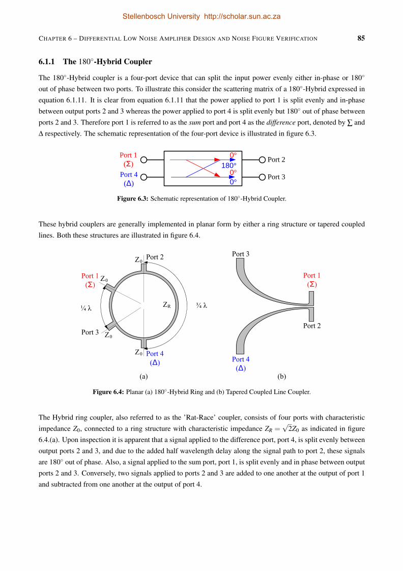
CHAPTER 6 – DIFFERENTIAL LOW NOISE AMPLIFIER DESIGN AND NOISE FIGURE VERIFICATION 85
6.1.1 The 180-Hybrid Coupler
The 180-Hybrid coupler is a four-port device that can split the input power evenly either in-phase or 180
out of phase between two ports. To illustrate this consider the scattering matrix of a 180-Hybrid expressed in
equation 6.1.11. It is clear from equation 6.1.11 that the power applied to port 1 is split evenly and in-phase
between output ports 2 and 3 whereas the power applied to port 4 is split evenly but 180 out of phase between
ports 2 and 3. Therefore port 1 is referred to as the sum port and port 4 as the difference port, denoted by ∑ and
∆ respectively. The schematic representation of the four-port device is illustrated in figure 6.3.
Port 1(Σ) Port 2
Port 3Port 4(∆)
0°
0°0°
180°
Figure 6.3: Schematic representation of 180-Hybrid Coupler.
These hybrid couplers are generally implemented in planar form by either a ring structure or tapered coupled
lines. Both these structures are illustrated in figure 6.4.
Port 4(∆)
Port 1(Σ)
Port 2
Port 3
¾ λ¼ λ
Port 2
Port 3
Port 1(Σ)
Port 4(∆)
ZR
Z0
Z0
Z0
Z0
(a) (b)
Figure 6.4: Planar (a) 180-Hybrid Ring and (b) Tapered Coupled Line Coupler.
The Hybrid ring coupler, also referred to as the ’Rat-Race’ coupler, consists of four ports with characteristic
impedance Z0, connected to a ring structure with characteristic impedance ZR =√
2Z0 as indicated in figure
6.4.(a). Upon inspection it is apparent that a signal applied to the difference port, port 4, is split evenly between
output ports 2 and 3, and due to the added half wavelength delay along the signal path to port 2, these signals
are 180 out of phase. Also, a signal applied to the sum port, port 1, is split evenly and in phase between output
ports 2 and 3. Conversely, two signals applied to ports 2 and 3 are added to one another at the output of port 1
and subtracted from one another at the output of port 4.
Stellenbosch University http://scholar.sun.ac.za
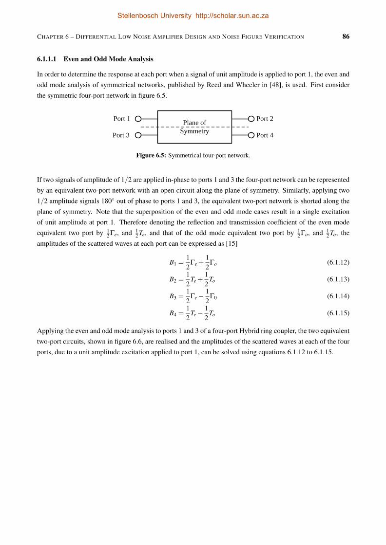
CHAPTER 6 – DIFFERENTIAL LOW NOISE AMPLIFIER DESIGN AND NOISE FIGURE VERIFICATION 86
6.1.1.1 Even and Odd Mode Analysis
In order to determine the response at each port when a signal of unit amplitude is applied to port 1, the even and
odd mode analysis of symmetrical networks, published by Reed and Wheeler in [48], is used. First consider
the symmetric four-port network in figure 6.5.
Port 1 Port 2
Port 4Port 3
Plane of Symmetry
Figure 6.5: Symmetrical four-port network.
If two signals of amplitude of 1/2 are applied in-phase to ports 1 and 3 the four-port network can be represented
by an equivalent two-port network with an open circuit along the plane of symmetry. Similarly, applying two
1/2 amplitude signals 180 out of phase to ports 1 and 3, the equivalent two-port network is shorted along the
plane of symmetry. Note that the superposition of the even and odd mode cases result in a single excitation
of unit amplitude at port 1. Therefore denoting the reflection and transmission coefficient of the even mode
equivalent two port by 12 Γe, and 1
2 Te, and that of the odd mode equivalent two port by 12 Γo, and 1
2 To, the
amplitudes of the scattered waves at each port can be expressed as [15]
B1 =12
Γe +12
Γo (6.1.12)
B2 =12
Te +12
To (6.1.13)
B3 =12
Γe−12
Γ0 (6.1.14)
B4 =12
Te−12
To (6.1.15)
Applying the even and odd mode analysis to ports 1 and 3 of a four-port Hybrid ring coupler, the two equivalent
two-port circuits, shown in figure 6.6, are realised and the amplitudes of the scattered waves at each of the four
ports, due to a unit amplitude excitation applied to port 1, can be solved using equations 6.1.12 to 6.1.15.
Stellenbosch University http://scholar.sun.ac.za
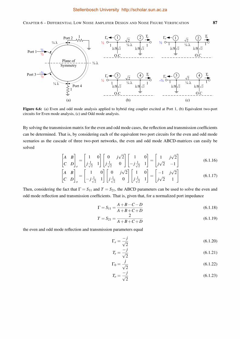
CHAPTER 6 – DIFFERENTIAL LOW NOISE AMPLIFIER DESIGN AND NOISE FIGURE VERIFICATION 87
¼ λ
O.C
λ/8 λ/8
½ 2
221 1
¼ λ
O.C
λ/8 λ/8
-½ 2
22
1 1
(b) (c)
¼ λ
O.C
λ/8 λ/8
½ 2
221 1
Port 1
Port 2
Port 3
Port 4
Plane of Symmetry
¼ λ
¼ λ
¾ λ
(a)
1
1
½
-½ ½
½
¼ λ
O.C
λ/8 λ/8
½ 2
22
1 1
1 2 1 2
3 4 3 4
Γe
Γe
Γo
Γo
Te
Te To
To
Figure 6.6: (a) Even and odd mode analysis applied to hybrid ring coupler excited at Port 1, (b) Equivalent two-portcircuits for Even mode analysis, (c) and Odd mode analysis.
By solving the transmission matrix for the even and odd mode cases, the reflection and transmission coefficients
can be determined. That is, by considering each of the equivalent two port circuits for the even and odd mode
scenarios as the cascade of three two-port networks, the even and odd mode ABCD-matrices can easily be
solved [A B
C D
]e
=
[1 0
j 1√2
1
][0 j
√2
j 1√2
0
][1 0
− j 1√2
1
]=
[1 j
√2
j√
2 −1
](6.1.16)[
A B
C D
]o
=
[1 0
− j 1√2
1
][0 j
√2
j 1√2
0
][1 0
j 1√2
1
]=
[−1 j
√2
j√
2 1
](6.1.17)
Then, considering the fact that Γ = S11 and T = S21, the ABCD parameters can be used to solve the even and
odd mode reflection and transmission coefficients. That is, given that, for a normalized port impedance
Γ = S11 =A+B−C−DA+B+C+D
(6.1.18)
T = S21 =2
A+B+C+D(6.1.19)
the even and odd mode reflection and transmission parameters equal
Γe =− j√
2(6.1.20)
Te =− j√
2(6.1.21)
Γ0 =j√2
(6.1.22)
To =− j√
2(6.1.23)
Stellenbosch University http://scholar.sun.ac.za
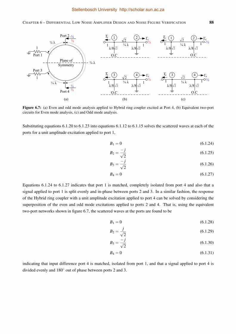
CHAPTER 6 – DIFFERENTIAL LOW NOISE AMPLIFIER DESIGN AND NOISE FIGURE VERIFICATION 88
¼ λ
O.C
λ/8 λ/8
2
221 1
¼ λ
O.C
λ/8 λ/8
2
22
1 1
(b) (c)
¼ λ
O.C
λ/8 λ/8
2
221 1
Port 1
Port 2
Port 3
Port 4
Plane of Symmetry
¼ λ
¼ λ
¾ λ
(a)
¼ λ
O.C
λ/8 λ/8
2
22
1 1
1 2 1 2
3 4 3 4ΓeTe
1
1
½
½ -½
½
-½ To Γo
½ Γo
To
½
½
Te Γe
Figure 6.7: (a) Even and odd mode analysis applied to Hybrid ring coupler excited at Port 4, (b) Equivalent two-portcircuits for Even mode analysis, (c) and Odd mode analysis.
Substituting equations 6.1.20 to 6.1.23 into equations 6.1.12 to 6.1.15 solves the scattered waves at each of the
ports for a unit amplitude excitation applied to port 1,
B1 = 0 (6.1.24)
B2 =− j√
2(6.1.25)
B3 =− j√
2(6.1.26)
B4 = 0 (6.1.27)
Equations 6.1.24 to 6.1.27 indicates that port 1 is matched, completely isolated from port 4 and also that a
signal applied to port 1 is split evenly and in-phase between ports 2 and 3. In a similar fashion, the response
of the Hybrid ring coupler with a unit amplitude excitation applied to port 4 can be solved by considering the
superposition of the even and odd mode excitations applied to ports 2 and 4. That is, using the equivalent
two-port networks shown in figure 6.7, the scattered waves at the ports are found to be
B1 = 0 (6.1.28)
B2 =j√2
(6.1.29)
B3 =− j√
2(6.1.30)
B4 = 0 (6.1.31)
indicating that input difference port 4 is matched, isolated from port 1, and that a signal applied to port 4 is
divided evenly and 180 out of phase between ports 2 and 3.
Stellenbosch University http://scholar.sun.ac.za
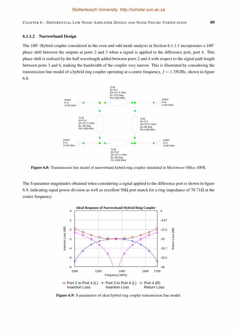
CHAPTER 6 – DIFFERENTIAL LOW NOISE AMPLIFIER DESIGN AND NOISE FIGURE VERIFICATION 89
6.1.1.2 Narrowband Design
The 180-Hybrid coupler considered in the even and odd mode analysis in Section 6.1.1.1 incorporates a 180
phase shift between the outputs at ports 2 and 3 when a signal is applied to the difference port, port 4. This
phase shift is realised by the half wavelength added between ports 2 and 4 with respect to the signal path length
between ports 3 and 4, making the bandwidth of the coupler very narrow. This is illustrated by considering the
transmission line model of a hybrid ring coupler operating at a centre frequency, f = 1.35GHz, shown in figure
6.8.
TLINID=TL1Z0=70.71 OhmEL=270 DegF0=1350 MHz
TLINID=TL2Z0=70.71 OhmEL=90 DegF0=1350 MHz
TLINID=TL3Z0=70.71 OhmEL=90 DegF0=1350 MHz
TLINID=TL4Z0=70.71 OhmEL=90 DegF0=1350 MHz
PORTP=3Z=50 Ohm
PORTP=4Z=50 Ohm
PORTP=2Z=50 Ohm
PORTP=1Z=50 Ohm
Figure 6.8: Transmission line model of narrowband hybrid ring coupler simulated in Microwave Office AWR.
The S-paramter magnitudes obtained when considering a signal applied to the difference port is shown in figure
6.9, indicating equal power division as well as excellent 50Ω port match for a ring impedance of 70.71Ω at the
center frequency.
1000 1200 1400 1600 1700Frequency (MHz)
Ideal Response of Narrowband Hybrid Ring Coupler
-6
-5
-4
-3
-2
-1
0
Inse
rtion
Los
s (d
B)
-40
-33.3
-26.7
-20
-13.3
-6.67
0
Ret
urn
Loss
(dB
)
Port 2 to Port 4 (L)Insertion Loss
Port 3 to Port 4 (L)Insertion Loss
Port 4 (R)Return Loss
Figure 6.9: S-parameters of ideal hybrid ring coupler transmission line model.
Stellenbosch University http://scholar.sun.ac.za
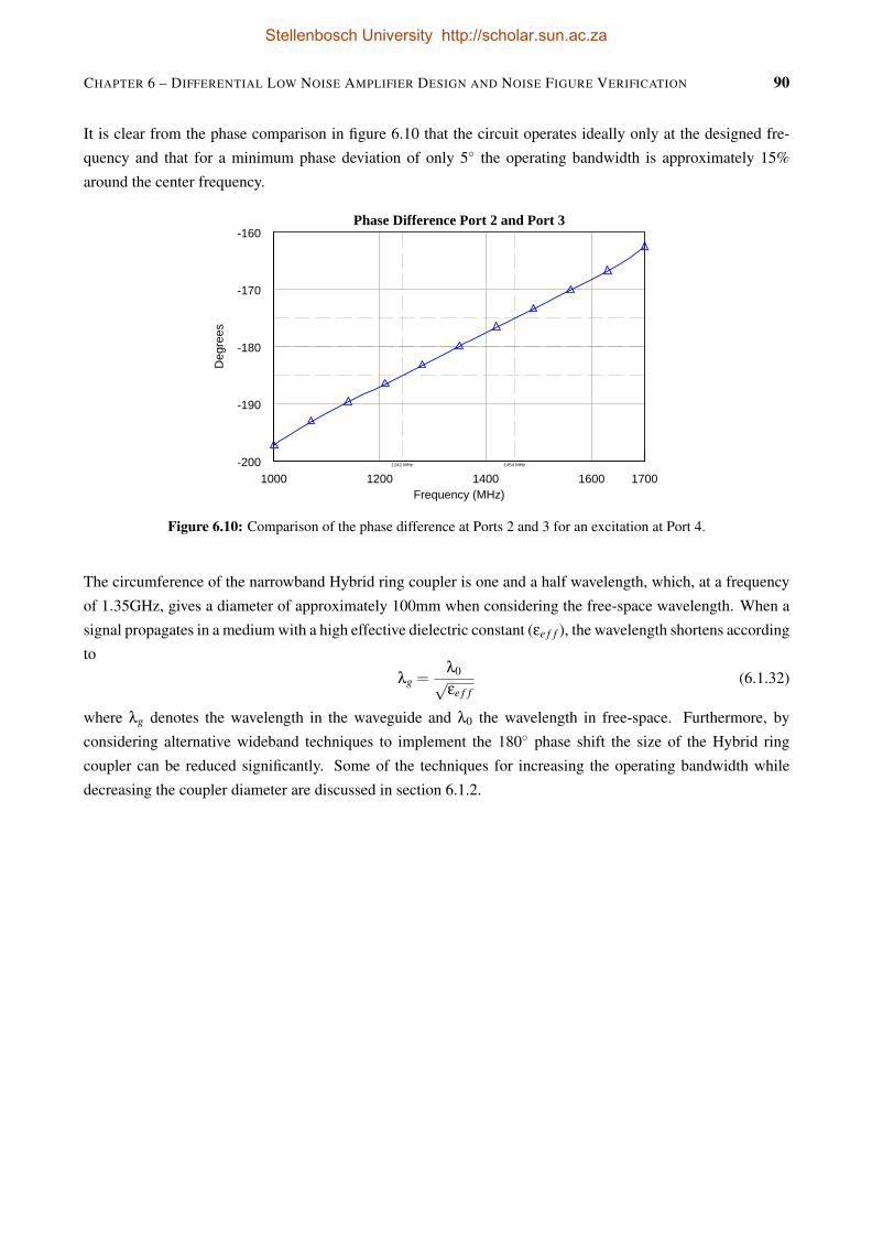
CHAPTER 6 – DIFFERENTIAL LOW NOISE AMPLIFIER DESIGN AND NOISE FIGURE VERIFICATION 90
It is clear from the phase comparison in figure 6.10 that the circuit operates ideally only at the designed fre-
quency and that for a minimum phase deviation of only 5 the operating bandwidth is approximately 15%
around the center frequency.
1000 1200 1400 1600 1700Frequency (MHz)
Phase Difference Port 2 and Port 3
-200
-190
-180
-170
-160D
egre
es
1454 MHz1242 MHz
Figure 6.10: Comparison of the phase difference at Ports 2 and 3 for an excitation at Port 4.
The circumference of the narrowband Hybrid ring coupler is one and a half wavelength, which, at a frequency
of 1.35GHz, gives a diameter of approximately 100mm when considering the free-space wavelength. When a
signal propagates in a medium with a high effective dielectric constant (εe f f ), the wavelength shortens according
to
λg =λ0√εe f f
(6.1.32)
where λg denotes the wavelength in the waveguide and λ0 the wavelength in free-space. Furthermore, by
considering alternative wideband techniques to implement the 180 phase shift the size of the Hybrid ring
coupler can be reduced significantly. Some of the techniques for increasing the operating bandwidth while
decreasing the coupler diameter are discussed in section 6.1.2.
Stellenbosch University http://scholar.sun.ac.za
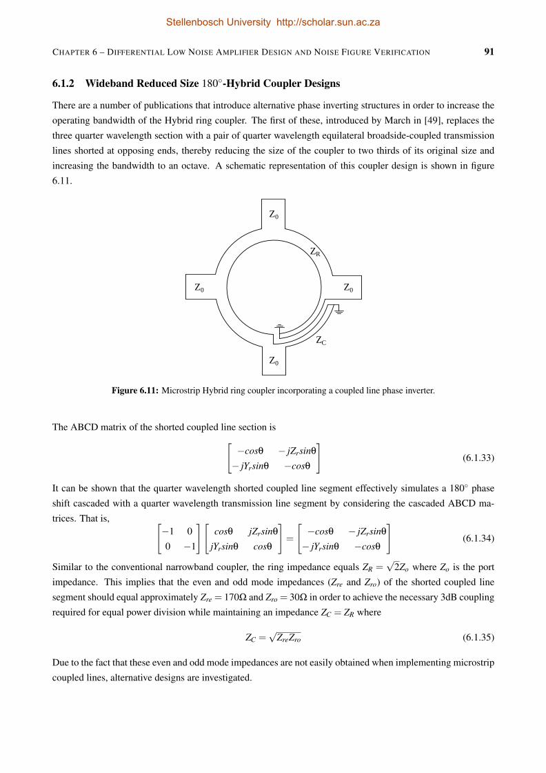
CHAPTER 6 – DIFFERENTIAL LOW NOISE AMPLIFIER DESIGN AND NOISE FIGURE VERIFICATION 91
6.1.2 Wideband Reduced Size 180-Hybrid Coupler Designs
There are a number of publications that introduce alternative phase inverting structures in order to increase the
operating bandwidth of the Hybrid ring coupler. The first of these, introduced by March in [49], replaces the
three quarter wavelength section with a pair of quarter wavelength equilateral broadside-coupled transmission
lines shorted at opposing ends, thereby reducing the size of the coupler to two thirds of its original size and
increasing the bandwidth to an octave. A schematic representation of this coupler design is shown in figure
6.11.
Z0
Z0Z0
Z0
ZR
ZC
Figure 6.11: Microstrip Hybrid ring coupler incorporating a coupled line phase inverter.
The ABCD matrix of the shorted coupled line section is[−cosθ − jZrsinθ
− jYrsinθ −cosθ
](6.1.33)
It can be shown that the quarter wavelength shorted coupled line segment effectively simulates a 180 phase
shift cascaded with a quarter wavelength transmission line segment by considering the cascaded ABCD ma-
trices. That is, [−1 0
0 −1
][cosθ jZrsinθ
jYrsinθ cosθ
]=
[−cosθ − jZrsinθ
− jYrsinθ −cosθ
](6.1.34)
Similar to the conventional narrowband coupler, the ring impedance equals ZR =√
2Zo where Zo is the port
impedance. This implies that the even and odd mode impedances (Zre and Zro) of the shorted coupled line
segment should equal approximately Zre = 170Ω and Zro = 30Ω in order to achieve the necessary 3dB coupling
required for equal power division while maintaining an impedance ZC = ZR where
ZC =√
ZreZro (6.1.35)
Due to the fact that these even and odd mode impedances are not easily obtained when implementing microstrip
coupled lines, alternative designs are investigated.
Stellenbosch University http://scholar.sun.ac.za
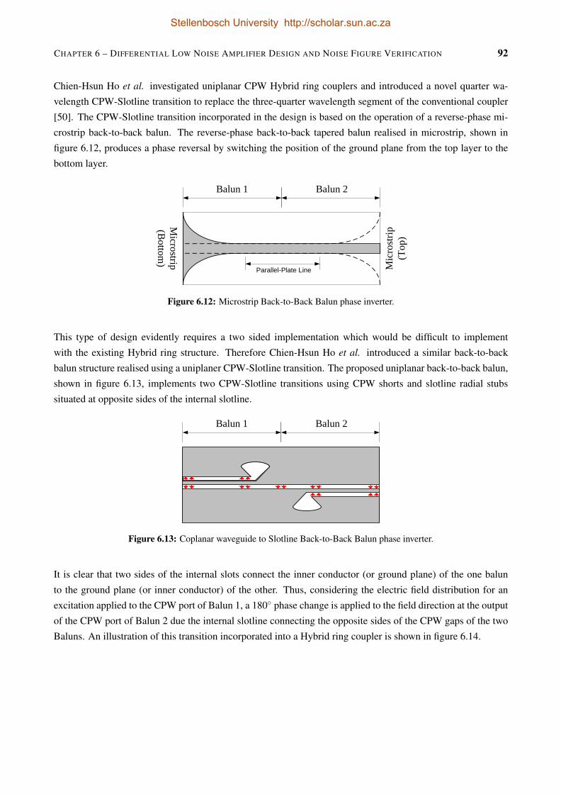
CHAPTER 6 – DIFFERENTIAL LOW NOISE AMPLIFIER DESIGN AND NOISE FIGURE VERIFICATION 92
Chien-Hsun Ho et al. investigated uniplanar CPW Hybrid ring couplers and introduced a novel quarter wa-
velength CPW-Slotline transition to replace the three-quarter wavelength segment of the conventional coupler
[50]. The CPW-Slotline transition incorporated in the design is based on the operation of a reverse-phase mi-
crostrip back-to-back balun. The reverse-phase back-to-back tapered balun realised in microstrip, shown in
figure 6.12, produces a phase reversal by switching the position of the ground plane from the top layer to the
bottom layer.
Balun 1 Balun 2
Parallel-Plate Line
Microstrip
(Bottom
) Mic
rost
rip(T
op)
Figure 6.12: Microstrip Back-to-Back Balun phase inverter.
This type of design evidently requires a two sided implementation which would be difficult to implement
with the existing Hybrid ring structure. Therefore Chien-Hsun Ho et al. introduced a similar back-to-back
balun structure realised using a uniplaner CPW-Slotline transition. The proposed uniplanar back-to-back balun,
shown in figure 6.13, implements two CPW-Slotline transitions using CPW shorts and slotline radial stubs
situated at opposite sides of the internal slotline.
Balun 1 Balun 2
Figure 6.13: Coplanar waveguide to Slotline Back-to-Back Balun phase inverter.
It is clear that two sides of the internal slots connect the inner conductor (or ground plane) of the one balun
to the ground plane (or inner conductor) of the other. Thus, considering the electric field distribution for an
excitation applied to the CPW port of Balun 1, a 180 phase change is applied to the field direction at the output
of the CPW port of Balun 2 due the internal slotline connecting the opposite sides of the CPW gaps of the two
Baluns. An illustration of this transition incorporated into a Hybrid ring coupler is shown in figure 6.14.
Stellenbosch University http://scholar.sun.ac.za
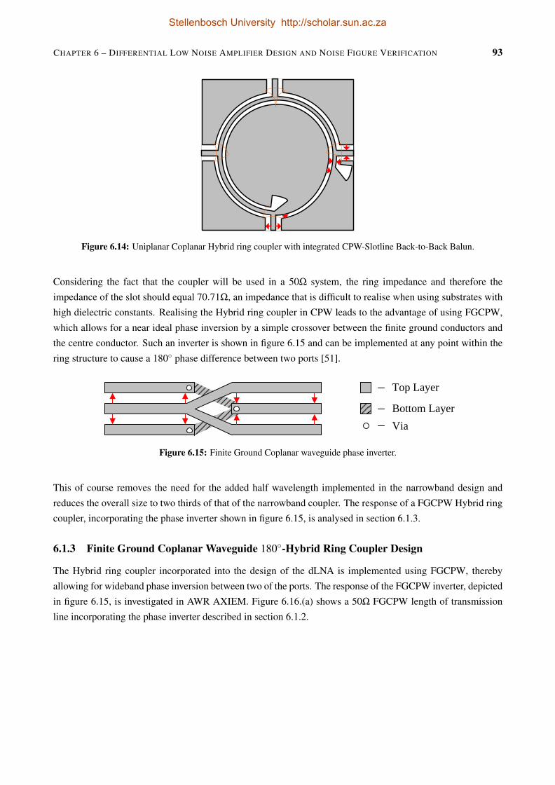
CHAPTER 6 – DIFFERENTIAL LOW NOISE AMPLIFIER DESIGN AND NOISE FIGURE VERIFICATION 93
Figure 6.14: Uniplanar Coplanar Hybrid ring coupler with integrated CPW-Slotline Back-to-Back Balun.
Considering the fact that the coupler will be used in a 50Ω system, the ring impedance and therefore the
impedance of the slot should equal 70.71Ω, an impedance that is difficult to realise when using substrates with
high dielectric constants. Realising the Hybrid ring coupler in CPW leads to the advantage of using FGCPW,
which allows for a near ideal phase inversion by a simple crossover between the finite ground conductors and
the centre conductor. Such an inverter is shown in figure 6.15 and can be implemented at any point within the
ring structure to cause a 180 phase difference between two ports [51].
Top Layer
Bottom LayerVia
Figure 6.15: Finite Ground Coplanar waveguide phase inverter.
This of course removes the need for the added half wavelength implemented in the narrowband design and
reduces the overall size to two thirds of that of the narrowband coupler. The response of a FGCPW Hybrid ring
coupler, incorporating the phase inverter shown in figure 6.15, is analysed in section 6.1.3.
6.1.3 Finite Ground Coplanar Waveguide 180-Hybrid Ring Coupler Design
The Hybrid ring coupler incorporated into the design of the dLNA is implemented using FGCPW, thereby
allowing for wideband phase inversion between two of the ports. The response of the FGCPW inverter, depicted
in figure 6.15, is investigated in AWR AXIEM. Figure 6.16.(a) shows a 50Ω FGCPW length of transmission
line incorporating the phase inverter described in section 6.1.2.
Stellenbosch University http://scholar.sun.ac.za
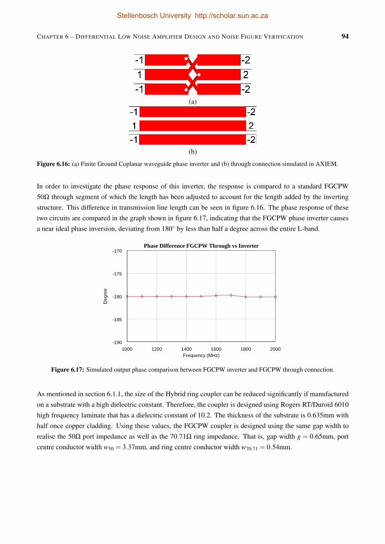
CHAPTER 6 – DIFFERENTIAL LOW NOISE AMPLIFIER DESIGN AND NOISE FIGURE VERIFICATION 94
(a)
(b)
Figure 6.16: (a) Finite Ground Coplanar waveguide phase inverter and (b) through connection simulated in AXIEM.
In order to investigate the phase response of this inverter, the response is compared to a standard FGCPW
50Ω through segment of which the length has been adjusted to account for the length added by the inverting
structure. This difference in transmission line length can be seen in figure 6.16. The phase response of these
two circuits are compared in the graph shown in figure 6.17, indicating that the FGCPW phase inverter causes
a near ideal phase inversion, deviating from 180 by less than half a degree across the entire L-band.
1000 1200 1400 1600 1800 2000Frequency (MHz)
Phase Difference FGCPW Through vs Inverter
-190
-185
-180
-175
-170
Deg
ree
Figure 6.17: Simulated output phase comparison between FGCPW inverter and FGCPW through connection.
As mentioned in section 6.1.1, the size of the Hybrid ring coupler can be reduced significantly if manufactured
on a substrate with a high dielectric constant. Therefore, the coupler is designed using Rogers RT/Duroid 6010
high frequency laminate that has a dielectric constant of 10.2. The thickness of the substrate is 0.635mm with
half once copper cladding. Using these values, the FGCPW coupler is designed using the same gap width to
realise the 50Ω port impedance as well as the 70.71Ω ring impedance. That is, gap width g = 0.65mm, port
centre conductor width w50 = 3.37mm, and ring centre conductor width w70.71 = 0.54mm.
Stellenbosch University http://scholar.sun.ac.za
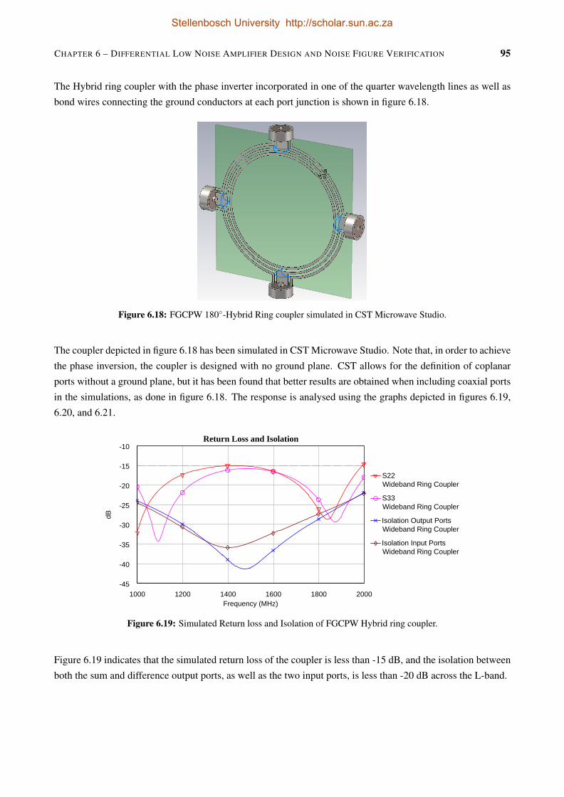
CHAPTER 6 – DIFFERENTIAL LOW NOISE AMPLIFIER DESIGN AND NOISE FIGURE VERIFICATION 95
The Hybrid ring coupler with the phase inverter incorporated in one of the quarter wavelength lines as well as
bond wires connecting the ground conductors at each port junction is shown in figure 6.18.CST MICROWAVE STUDIO *** Educational Version *** 09/07/2011 - 23:50
File: D:\MScIng_2011\CST\Thesis\WidebandRatRace_104lambda.cst
Figure 6.18: FGCPW 180-Hybrid Ring coupler simulated in CST Microwave Studio.
The coupler depicted in figure 6.18 has been simulated in CST Microwave Studio. Note that, in order to achieve
the phase inversion, the coupler is designed with no ground plane. CST allows for the definition of coplanar
ports without a ground plane, but it has been found that better results are obtained when including coaxial ports
in the simulations, as done in figure 6.18. The response is analysed using the graphs depicted in figures 6.19,
6.20, and 6.21.
1000 1200 1400 1600 1800 2000Frequency (MHz)
Return Loss and Isolation
-45
-40
-35
-30
-25
-20
-15
-10
dB
S22Wideband Ring Coupler
S33Wideband Ring Coupler
Isolation Output PortsWideband Ring Coupler
Isolation Input PortsWideband Ring Coupler
Figure 6.19: Simulated Return loss and Isolation of FGCPW Hybrid ring coupler.
Figure 6.19 indicates that the simulated return loss of the coupler is less than -15 dB, and the isolation between
both the sum and difference output ports, as well as the two input ports, is less than -20 dB across the L-band.
Stellenbosch University http://scholar.sun.ac.za
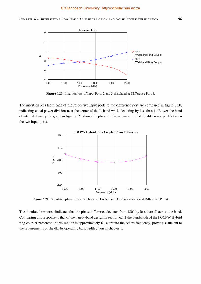
CHAPTER 6 – DIFFERENTIAL LOW NOISE AMPLIFIER DESIGN AND NOISE FIGURE VERIFICATION 96
1000 1200 1400 1600 1800 2000Frequency (MHz)
Insertion Loss
-5
-4
-3
-2
-1
0
dB
S43Wideband Ring Coupler
S42Wideband Ring Coupler
Figure 6.20: Insertion loss of Input Ports 2 and 3 simulated at Difference Port 4.
The insertion loss from each of the respective input ports to the difference port are compared in figure 6.20,
indicating equal power division near the center of the L-band while deviating by less than 1 dB over the band
of interest. Finally the graph in figure 6.21 shows the phase difference measured at the difference port between
the two input ports.
1000 1200 1400 1600 1800 2000Frequency (MHz)
FGCPW Hybrid Ring Coupler Phase Difference
-200
-190
-180
-170
-160
Deg
ree
Figure 6.21: Simulated phase difference between Ports 2 and 3 for an excitation at Difference Port 4.
The simulated response indicates that the phase difference deviates from 180 by less than 5 across the band.
Comparing this response to that of the narrowband design in section 6.1.1 the bandwidth of the FGCPW Hybrid
ring coupler presented in this section is approximately 67% around the centre frequency, proving sufficient to
the requirements of the dLNA operating bandwidth given in chapter 1.
Stellenbosch University http://scholar.sun.ac.za
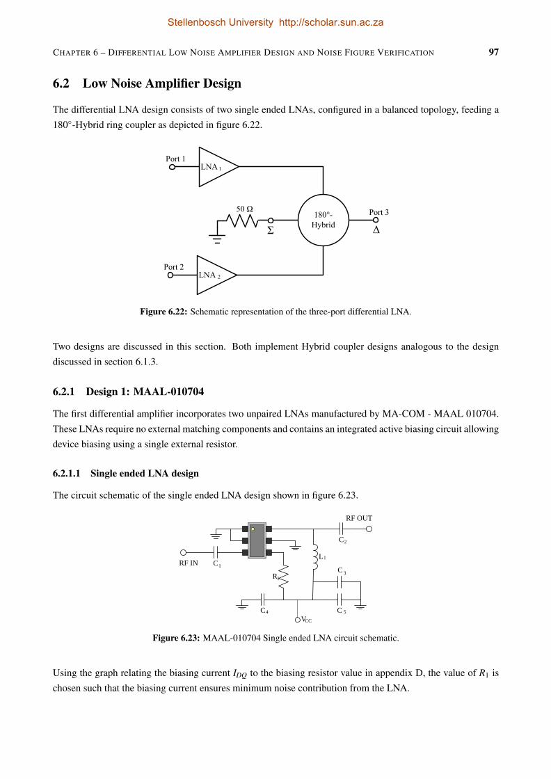
CHAPTER 6 – DIFFERENTIAL LOW NOISE AMPLIFIER DESIGN AND NOISE FIGURE VERIFICATION 97
6.2 Low Noise Amplifier Design
The differential LNA design consists of two single ended LNAs, configured in a balanced topology, feeding a
180-Hybrid ring coupler as depicted in figure 6.22.
180°-Hybrid
LNA 1
50 Ω
ΔΣ
LNA 2
Port 1
Port 2
Port 3
Figure 6.22: Schematic representation of the three-port differential LNA.
Two designs are discussed in this section. Both implement Hybrid coupler designs analogous to the design
discussed in section 6.1.3.
6.2.1 Design 1: MAAL-010704
The first differential amplifier incorporates two unpaired LNAs manufactured by MA-COM - MAAL 010704.
These LNAs require no external matching components and contains an integrated active biasing circuit allowing
device biasing using a single external resistor.
6.2.1.1 Single ended LNA design
The circuit schematic of the single ended LNA design shown in figure 6.23.
CL
R
C
C
C C
RF IN
RF OUT
1
2
1
1
3
4 5VCC
Figure 6.23: MAAL-010704 Single ended LNA circuit schematic.
Using the graph relating the biasing current IDQ to the biasing resistor value in appendix D, the value of R1 is
chosen such that the biasing current ensures minimum noise contribution from the LNA.
Stellenbosch University http://scholar.sun.ac.za
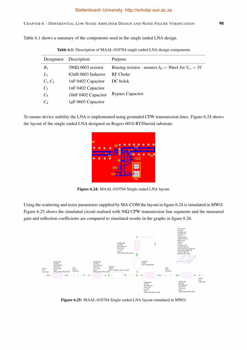
CHAPTER 6 – DIFFERENTIAL LOW NOISE AMPLIFIER DESIGN AND NOISE FIGURE VERIFICATION 98
Table 6.1 shows a summary of the components used in the single ended LNA design.
Table 6.1: Description of MAAL-010704 single ended LNA design components
Designator Description Purpose
R1 390Ω 0603 resistor Biasing resistor - ensures ID = 30mA for Vcc = 3V
L1 82nH 0603 Inductor RF Choke
C1,C2 1nF 0402 Capacitor DC bolck
C3 1nF 0402 CapacitorBypass CapacitorC5 10nF 0402 Capacitor
C4 1µF 0603 Capacitor
To ensure device stability the LNA is implemented using grounded CPW transmission lines. Figure 6.24 shows
the layout of the single ended LNA designed on Rogers 6010 RT/Duroid substrate.
Figure 6.24: MAAL-010704 Single ended LNA layout.
Using the scattering and noise parameters supplied by MA-COM the layout in figure 6.24 is simulated in MWO.
Figure 6.25 shows the simulated circuit realised with 50Ω CPW transmission line segments and the measured
gain and reflection coefficients are compared to simulated results in the graphs in figure 6.26.
CAPID=C1C=1e-9 F
CPW1LINEID=CP1W=0.488 mmS=0.5 mmL=4 mmAcc=1CPW_SUB=CPW_SUB1
CPW1LINEID=CP3W=0.488 mmS=0.5 mmL=1.7 mmAcc=1CPW_SUB=CPW_SUB1
CPW1LINEID=CP6W=0.488 mmS=0.5 mmL=5.6 mmAcc=1CPW_SUB=CPW_SUB1
CPW1LINEID=CP8W=0.488 mmS=0.5 mmL=5.57 mmAcc=1CPW_SUB=CPW_SUB1
CPW1LINEID=CP9W=0.488 mmS=0.5 mmL=7 mmAcc=1CPW_SUB=CPW_SUB1
CPW_SUBEr=10.2H=0.635 mmT=0.018 mmRho=0.7Tand=0.0023Hcover=10 mmHab=2 mmCover=1Gnd=1Er_Nom=3.38H_Nom=H@ mmHcov_Nom=Hcover@ mmHab_Nom=Hab@ mmT_Nom=T@ mmName=CPW_SUB1
CAPID=C2C=1e-9 F
1
2
SUBCKTID=S6NET="04HPH82N"
1 2
SUBCKTID=S1NET="XG1015_SE_3V_30mA"
PORTP=1Z=50 Ohm
PORTP=2Z=50 Ohm
Figure 6.25: MAAL-010704 Single ended LNA layout simulated in MWO.
Stellenbosch University http://scholar.sun.ac.za

CHAPTER 6 – DIFFERENTIAL LOW NOISE AMPLIFIER DESIGN AND NOISE FIGURE VERIFICATION 99
1000 1100 1200 1300 1400 1500 1600 17000
5
10
15
20MAAL-010704 Single Ended LNA Gain
Frequency (MHz)
|S21
| (dB
)
MeasuredSimulated
1000 1100 1200 1300 1400 1500 1600 1700-30
-25
-20
-15
-10
-5
0MAAL-010704 Single Ended LNA Reflection Coefficients
Frequency (MHz)
Ref
lect
ion
Coe
ffic
ient
(dB
)
Measured |S11|Simulated |S11|Measured |S22|Simulated |S22|
(a) (b)
Figure 6.26: Simulated (a) Gain and (b) Reflection Coefficients of MAAL-010704 Single ended LNA.
Due to the low noise figure of the LNA, the noise figure is measured using the configuration depicted in figure
5.13. Figure 6.27 compares the measured narrowband noise figure to the simulated results.
1000 1100 1200 1300 1400 1500 1600 17000
0.2
0.4
0.6
0.8
1
1.2
1.4
1.6
1.8
2MAAL-010704 Single Ended LNA Noise Figure
Frequency (MHz)
(dB
)
MeasuredSimulated
Figure 6.27: MAAL-010704 Single ended LNA noise figure.
The graph comparing the reflection coefficients in figure 6.26(b) indicates that the input and output match of
the manufactured LNA differs slightly from that of the simulated circuit. The effect of this mismatch becomes
apparent when considering the deviation in gain and noise figure illustrated in figures 6.26(a) and 6.27 respec-
tively.
Stellenbosch University http://scholar.sun.ac.za
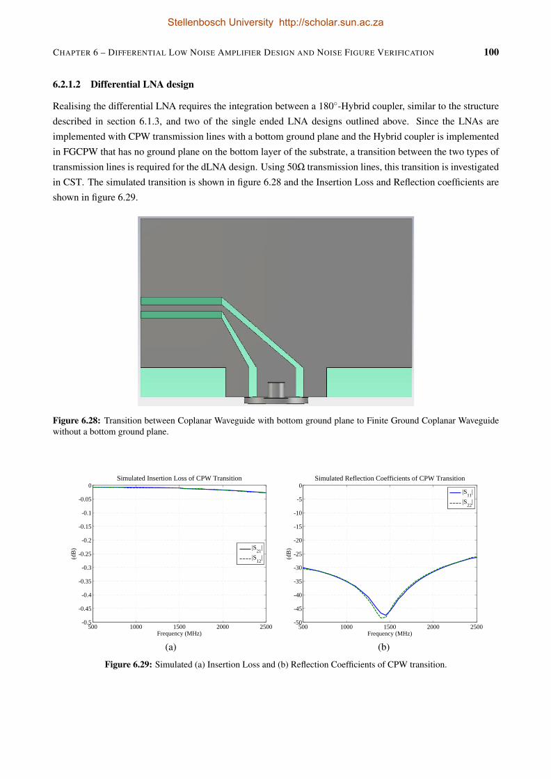
CHAPTER 6 – DIFFERENTIAL LOW NOISE AMPLIFIER DESIGN AND NOISE FIGURE VERIFICATION 100
6.2.1.2 Differential LNA design
Realising the differential LNA requires the integration between a 180-Hybrid coupler, similar to the structure
described in section 6.1.3, and two of the single ended LNA designs outlined above. Since the LNAs are
implemented with CPW transmission lines with a bottom ground plane and the Hybrid coupler is implemented
in FGCPW that has no ground plane on the bottom layer of the substrate, a transition between the two types of
transmission lines is required for the dLNA design. Using 50Ω transmission lines, this transition is investigated
in CST. The simulated transition is shown in figure 6.28 and the Insertion Loss and Reflection coefficients are
shown in figure 6.29.
CST MICROWAVE STUDIO *** Educational Version *** 09/16/2011 - 00:18
File: D:\MScIng_2011\CST\Thesis\cpw2fgcpw_coax.cst
Figure 6.28: Transition between Coplanar Waveguide with bottom ground plane to Finite Ground Coplanar Waveguidewithout a bottom ground plane.
500 1000 1500 2000 2500-0.5
-0.45
-0.4
-0.35
-0.3
-0.25
-0.2
-0.15
-0.1
-0.05
0Simulated Insertion Loss of CPW Transition
Frequency (MHz)
(dB
)
|S21
||S
12|
500 1000 1500 2000 2500-50
-45
-40
-35
-30
-25
-20
-15
-10
-5
0Simulated Reflection Coefficients of CPW Transition
Frequency (MHz)
(dB
)
|S11
||S
22|
(a) (b)
Figure 6.29: Simulated (a) Insertion Loss and (b) Reflection Coefficients of CPW transition.
Stellenbosch University http://scholar.sun.ac.za

CHAPTER 6 – DIFFERENTIAL LOW NOISE AMPLIFIER DESIGN AND NOISE FIGURE VERIFICATION 101
The dLNA design consisting of the two single ended LNAs connected to a 180-Hybrid coupler through a CPW
transition is shown in figure 6.30.
Figure 6.30: MAAL-010704 Differential LNA design layout.
6.2.1.3 Mixed-mode Signal Analysis
The theory on mixed mode S-parameters discussed in Chapter 4 can be applied to the three-port differential
LNA to analyse the response of the circuit for differential and common-mode excitation. It follows from the
relation in equation 4.3.32 that the mixed mode scattering matrix can be derived from the three-port scattering
matrix using the transformation matrix M. Where, analogous to equation 4.3.30, the three-port transformation
matrix equals
[M] =1√2
1 −1 0
1 1 0
0 0√
2
(6.2.1)
Then, from equation 4.3.32
Ss2d1 =1√2(S31−S32) (6.2.2)
Ss2c1 =1√2(S31 +S32) (6.2.3)
Sd1d1 =12(S22−S21−S12 +S11) (6.2.4)
Sc1c1 =12(S22 +S21 +S12 +S11) (6.2.5)
where the subscripts s, d, and c denote single ended, differential mode, and common-mode excitations. Equation
6.2.2 therefore equates the gain measured at the single ended output port due to a differential excitation applied
to the differential input port - comprising of single ended ports 1 and 2.
Stellenbosch University http://scholar.sun.ac.za
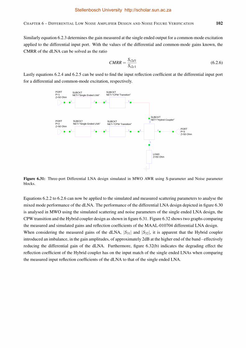
CHAPTER 6 – DIFFERENTIAL LOW NOISE AMPLIFIER DESIGN AND NOISE FIGURE VERIFICATION 102
Similarly equation 6.2.3 determines the gain measured at the single ended output for a common-mode excitation
applied to the differential input port. With the values of the differential and common-mode gains known, the
CMRR of the dLNA can be solved as the ratio
CMRR =Ss2d1
Ss2c1(6.2.6)
Lastly equations 6.2.4 and 6.2.5 can be used to find the input reflection coefficient at the differential input port
for a differential and common-mode excitation, respectively.
LOADZ=50 Ohm
12
SUBCKTNET="CPW Transition"
12
SUBCKTNET="CPW Transition"
1
2
3 4
SUBCKTNET="Hybrid Coupler"
1 2
SUBCKTNET="Single Ended LNA"
1 2
SUBCKTNET="Single Ended LNA"
PORTP=1Z=50 Ohm
PORTP=2Z=50 Ohm
PORTP=3Z=50 Ohm
Figure 6.31: Three-port Differential LNA design simulated in MWO AWR using S-parameter and Noise parameterblocks.
Equations 6.2.2 to 6.2.6 can now be applied to the simulated and measured scattering parameters to analyse the
mixed mode performance of the dLNA. The performance of the differential LNA design depicted in figure 6.30
is analysed in MWO using the simulated scattering and noise parameters of the single ended LNA design, the
CPW transition and the Hybrid coupler design as shown in figure 6.31. Figure 6.32 shows two graphs comparing
the measured and simulated gains and reflection coefficients of the MAAL-010704 differential LNA design.
When considering the measured gains of the dLNA, |S31| and |S32|, it is apparent that the Hybrid coupler
introduced an imbalance, in the gain amplitudes, of approximately 2dB at the higher end of the band - effectively
reducing the differential gain of the dLNA. Furthermore, figure 6.32(b) indicates the degrading effect the
reflection coefficient of the Hybrid coupler has on the input match of the single ended LNAs when comparing
the measured input reflection coefficients of the dLNA to that of the single ended LNA.
Stellenbosch University http://scholar.sun.ac.za

CHAPTER 6 – DIFFERENTIAL LOW NOISE AMPLIFIER DESIGN AND NOISE FIGURE VERIFICATION 103
1000 1100 1200 1300 1400 1500 1600 17000
5
10
15
20MAAL-010704 Differential LNA Gains
Frequency (MHz)
Gai
n (d
B)
Measured |S31|Simulated |S31|Measured |S32|Simulated |S32|Measured |Ss2d1|Simulated |Ss2d1|
1000 1100 1200 1300 1400 1500 1600 1700-15
-10
-5
0MAAL-010704 Differential LNA Input Reflection Coefficient
Frequency (MHz)
Ref
lect
ion
Coe
ffic
ient
(dB
)
Measured |S11|Simulated |S11|Measured |S22|Simulated |S22|Measured |Sd1d1|Single Ended LNA |S11|
(a) (b)
Figure 6.32: Simulated and measured (a) Gains and (b) Reflection Coefficients of the MAAL-010704 dLNA design.
1000 1100 1200 1300 1400 1500 1600 1700175
180
185MAAL-010704 Differential LNA Phase Difference
Frequency (MHz)
Phas
e Im
bala
nce
(Deg
rees
)
MeasuredSimulated
1000 1100 1200 1300 1400 1500 1600 17000
5
10
15
20
25
30
35
40MAAL-010704 Differential LNA Common Mode Rejection
Frequency (MHz)
CM
RR
(dB
)
MeasuredSimulated
(a) (b)
Figure 6.33: Simulated and measured (a) Phase imbalance and (b) CMRR of the MAAL-010704 dLNA design.
The phase imbalance and CMRR of the dLNA are shown in figure 6.33. The effect the deviation in insertion loss
of the coupler has on the performance of the dLNA can clearly be seen in the graph comparing the simulated
and measured CMRR, in figure 6.33(b). Even though the phase imbalance (figure 6.33(a)) varies by less than
three degrees across the band, the amplitude imbalance should ideally be centred around 0 dB to ensure a high
CMRR.
6.2.1.4 Mixed-mode Noise Analysis
Next consider the noise performance of the three-port dLNA. Chapter 3 discussed the derivation of the noise
correlation matrix for a multi-port network. The theory on mixed mode propagation, introduced in chapter 4,
can now be applied to the equivalent noisy three-port network shown in figure 6.34 to derive an expression for
the differential noise figure.
Stellenbosch University http://scholar.sun.ac.za
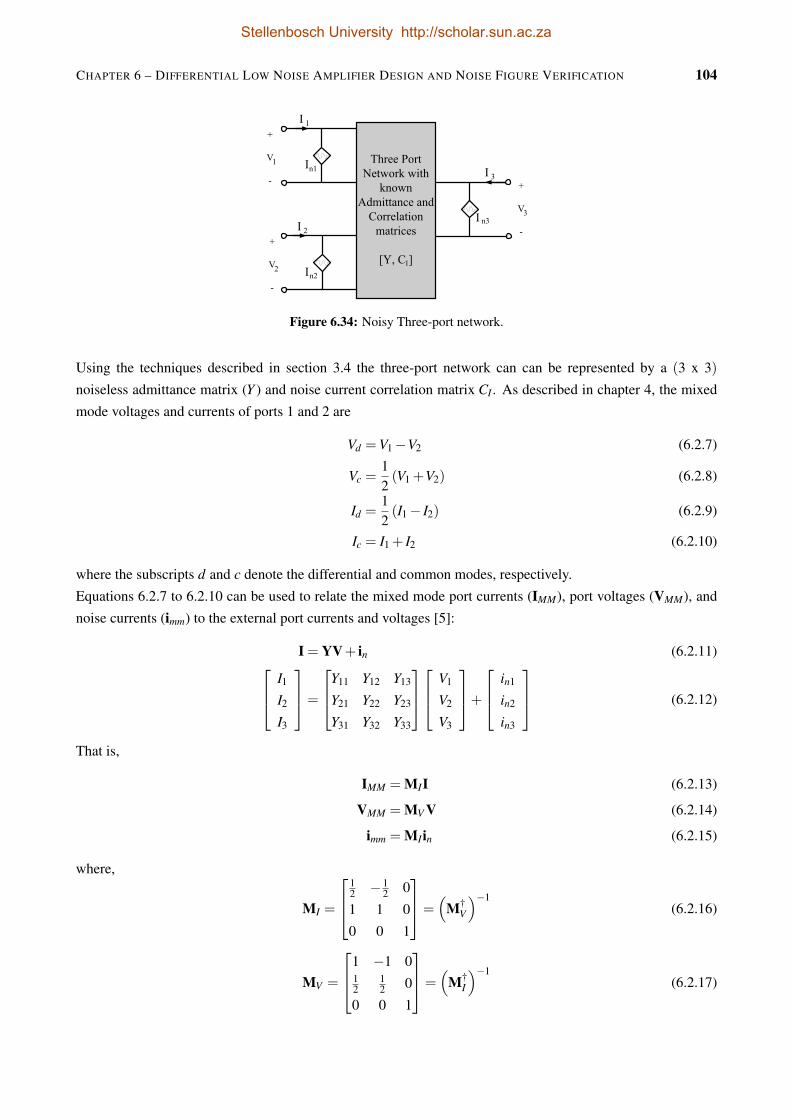
CHAPTER 6 – DIFFERENTIAL LOW NOISE AMPLIFIER DESIGN AND NOISE FIGURE VERIFICATION 104
I
Figure 6.34: Noisy Three-port network.
Using the techniques described in section 3.4 the three-port network can can be represented by a (3 x 3)
noiseless admittance matrix (Y ) and noise current correlation matrix CI . As described in chapter 4, the mixed
mode voltages and currents of ports 1 and 2 are
Vd =V1−V2 (6.2.7)
Vc =12(V1 +V2) (6.2.8)
Id =12(I1− I2) (6.2.9)
Ic = I1 + I2 (6.2.10)
where the subscripts d and c denote the differential and common modes, respectively.
Equations 6.2.7 to 6.2.10 can be used to relate the mixed mode port currents (IMM), port voltages (VMM), and
noise currents (imm) to the external port currents and voltages [5]:
I = YV+ in (6.2.11) I1
I2
I3
=
Y11 Y12 Y13
Y21 Y22 Y23
Y31 Y32 Y33
V1
V2
V3
+ in1
in2
in3
(6.2.12)
That is,
IMM = MII (6.2.13)
VMM = MV V (6.2.14)
imm = MIin (6.2.15)
where,
MI =
12 −1
2 0
1 1 0
0 0 1
=(
M†V
)−1(6.2.16)
MV =
1 −1 012
12 0
0 0 1
=(
M†I
)−1(6.2.17)
Stellenbosch University http://scholar.sun.ac.za
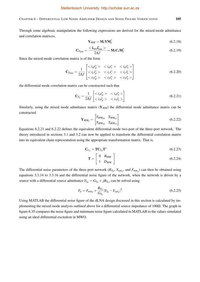
CHAPTER 6 – DIFFERENTIAL LOW NOISE AMPLIFIER DESIGN AND NOISE FIGURE VERIFICATION 105
Through some algebraic manipulation the following expressions are derived for the mixed-mode admittance
and correlation matrices,
YMM = MIYM†I (6.2.18)
CYMM =< immi∗mm >
2∆ f= MICIM†
I (6.2.19)
Since the mixed-mode correlation matrix is of the form
CYMM =1
2∆ f
< id i∗d > < id i∗c > < id i∗3 >
< ici∗d > < ici∗c > < ici∗3 >
< i3i∗d > < i3i∗c > < i3i∗3 >
(6.2.20)
the differential mode correlation matrix can be constructed such that
CYd =1
2∆ f
[< id i∗d > < id i∗3 >
< i3i∗d > < i3i∗3 >
](6.2.21)
Similarly, using the mixed mode admittance matrix (YMM) the differential mode admittance matrix can be
constructed
YMMd =
[YMMdd YMMd3
YMM3d YMM33
](6.2.22)
Equations 6.2.21 and 6.2.22 defines the equivalent differential-mode two-port of the three-port network. The
theory introduced in sections 3.1 and 3.2 can now be applied to transform the differential correlation matrix
into its equivalent chain representation using the appropriate transformation matrix. That is,
CCd = TCYd T† (6.2.23)
T =
[0 BMM
1 DMM
](6.2.24)
The differential noise parameters of the three-port network (RNd , Yoptd , and Fmind ) can then be obtained using
equations 3.3.14 to 3.3.16 and the differential noise figure of the network, when the network is driven by a
source with a differential source admittance YSd = GSd + jBSd , can be solved using
Fd = Fmind +RNd
GSd
|YSd −Yoptd |2 (6.2.25)
Using MATLAB the differential noise figure of the dLNA design discussed in this section is calculated by im-
plementing the mixed mode analysis outlined above for a differential source impedance of 100Ω. The graph in
figure 6.35 compares the noise figure and minimum noise figure calculated in MATLAB to the values simulated
using an ideal differential excitation in MWO.
Stellenbosch University http://scholar.sun.ac.za
CHAPTER 6 – DIFFERENTIAL LOW NOISE AMPLIFIER DESIGN AND NOISE FIGURE VERIFICATION 106
1 1.1 1.2 1.3 1.4 1.5 1.6 1.70
0.2
0.4
0.6
0.8
1
1.2
1.4
1.6
1.8
Frequency (GHz)
Noi
se F
igur
e (d
B)
Differential Noise Figure
Differential Noise Figure (MATLAB)Minimum Differential Noise Figure (MATLAB)Differential Noise Figure (MWO)Minimum Differential Noise Figure (MWO)
Figure 6.35: Differential noise figure and minimum differential noise figure calculated using mixed-mode analysis com-pared to simulated values.
Comparing the calculated differential noise figures to the simulated values indicates a discrepancy of approxi-
mately 0.1 dB between the values computed using the mixed-mode analysis and the simulated values. This
deviation can be ascribed to the accumulation of small rounding errors that occur throughout the implementa-
tion of the algorithm. Despite this deviation, the computed analysis still indicate - in agreement to the simulated
noise figure - that the dLNA design is well matched to a differential source impedance of 100Ω when conside-
ring the calculated and simulated differential noise figures individually compared to their respective minimum
noise figures.
Finally the noise performance of the dLNA design is investigated using the de-embedding technique described
in Chapter 5. The graph in figure 6.36(a) shows the single ended noise figure simulated when terminating each
of the input ports alternately. Then using equation 5.3.10 the simulated and measured differential noise figure
of the dLNA is de-embedded and compared to the noise figure of the constituent single ended LNA design in
figure 6.36(b). This dLNA design illustrates the importance of symmetry in the Hybrid coupler design. To
ensure that the signal performance of the differential LNA remains similar to that of the single ended LNAs it
comprises of, the amplitude imbalance of the coupler should ideally be near 0 dB within the band of interest.
Despite the deviation in the measured and simulated results, this design still verifies that the relation derived in
equation 5.3.10 can be used to de-embed the differential noise figure by taking the gain deviation into account.
Stellenbosch University http://scholar.sun.ac.za

CHAPTER 6 – DIFFERENTIAL LOW NOISE AMPLIFIER DESIGN AND NOISE FIGURE VERIFICATION 107
1000 1100 1200 1300 1400 1500 1600 17000
1
2
3
4
5MAAL-010704 Differential LNA Single ended Noise Figure
Frequency (MHz)
Noi
se F
igur
e (d
B)
Simulated F31:Port 2 TerminatedSimulated F32:Port 1 TerminatedMeasured F31Measured F32
1000 1100 1200 1300 1400 1500 1600 17000
0.5
1
1.5MAAL-010704 dLNA De-embedded Differential Noise Figure
Frequency (MHz)
Noi
se F
igur
e (d
B)
Simulated FdSimulated FsMeasured FdMeasured Fs
(a) (b)
Figure 6.36: Simulated and measured (a) single ended and (b) de-embedded differential noise figure of the MAAL-010704 dLNA design.
6.2.2 Design 2: MGA-16516
Given the results of the first differential LNA discussed in section 6.2.1, the inverter of the Hybrid coupler im-
plemented in the first dLNA has been altered to ensure improved amplitude imbalance. This involved reducing
the size of the the inverter gap and also making use of vias and conductor on the bottom layer of the substrate to
realise the inverter instead of lengthy bonding wires. The revised Hybrid coupler design is discussed in section
6.1.3 and is implemented in the second dLNA design discussed in this section. Implementing the dLNA using a
balanced topology has the advantage of considering the design of the constituent single ended LNAs separately.
Instead of using matched LNAs the transistors used for the single ended LNAs of this second dLNA design are
a pair of matched GaAs Enhancement-mode pseudomorphic High Electron Mobility Transistors (pHEMTs)
packaged in a 16-pin QFN package, manufactured by AVAGO Technologies: MGA-16516. During the design
of LNAs there are a number of fundamental constraints that the design must adhere to in order to ensure the
desired response, the first and most important of which is device stability.
6.2.3 Stability
A general two-port representation of an amplifier, defined by its S- and noise parameters, connected to a source
impedance ZS and terminated in a load impedance ZL is shown in figure 6.37.
[S]
ΓOUTΓL
Z L
ZS
ΓSΓIN
Figure 6.37: General representation of two-port amplifier network.
Stellenbosch University http://scholar.sun.ac.za

CHAPTER 6 – DIFFERENTIAL LOW NOISE AMPLIFIER DESIGN AND NOISE FIGURE VERIFICATION 108
The gain of the two-port network can be described by three different definitions: Power Gain (G), Available
Gain (GA), and Transducer Gain (GT ). The Power Gain relates the power dissipated in the load to the power
supplied to the input of the amplifier, and is therefore independent of the source impedance ZS. The Available
Gain is calculated as the ratio of the gain available at the output of the device to the power available from
the source. Available gain is therefore only dependent on the source impedance. Lastly, the Transducer Gain
is given by the ratio of the power dissipated in the load to the power available from the source. These gain
definitions aid in optimising the source and load matching conditions during amplifier design and it follows
that for conjugately matched two-port, G = GA = GT .
The input and output reflection coefficients can be solved in terms of the device S-parameters and the load and
source reflection coefficients, respectively. That is,
Γin = S11 +S12S21ΓL
1−S22ΓL(6.2.26)
Γout = S22 +S12S21ΓS
1−S11ΓS(6.2.27)
where the source and load reflection coefficients are solved by
ΓS =ZS−Z0
ZS +Z0(6.2.28)
ΓL =ZL−Z0
ZL +Z0(6.2.29)
The amplifier network is considered unconditionally stable if |Γin|< 1 and |Γout |< 1 for all passive source and
load impedances. If either |Γin|> 1 or |Γout |> 1 the network is considered conditionally stable and care should
be taken to present the device with a source or load impedance that will ensure stable operation.
For the device to be unconditionally stable the following condition, referred to as the µ−test, must be satisfied
µ =1−|S11|2
|S22−∆S∗11|+ |S12S21|> 1 (6.2.30)
This relation should hold over the full frequency range for which the device gain is greater than unity to ensure
that the amplifier does not oscillate at a frequency outside of its operating bandwidth. If it is found that µ < 1
over a range of frequencies, it is necessary to plot input and output stability circles in order to find the load
and source impedance values that will ensure stable operation. Note that these stability circles only apply to a
single frequency and therefore it may be necessary to plot a number of stability circles at intervals throughout
the potentially unstable region.
Consider the input stability circle plotted in the ΓS plane shown in figure 6.38.
The centre point and the radius of the stability circle are given by
CS =(S11−∆S∗22)
∗
|S11|2−|∆|2(6.2.31)
RS =
∣∣∣∣ S12S21
|S11|2−|∆|2
∣∣∣∣ (6.2.32)
where ∆ is defined as the determinant of the device scattering matrix
∆ = S11S22−S12S21 (6.2.33)
Stellenbosch University http://scholar.sun.ac.za

CHAPTER 6 – DIFFERENTIAL LOW NOISE AMPLIFIER DESIGN AND NOISE FIGURE VERIFICATION 109
0.33 1 30
-3j
-1j
-0.33j
0.33j
1j
3j
Figure 6.38: Input Stability circle plotted in ΓS Plane.
It follows from equation 6.2.26 that, if |S22|< 1 then |Γin|< 1 and hence that ΓS = 0 - the centre of the Smith
chart - indicates the stable region. Alternatively if |S22| > 1, then |Γin| > 1 indicating that the region in which
ΓS = 0 indicates the unstable region and therefore the stable impedances are found in the region of the input
stability circle that intersects the Smith chart.
Similarly the output stability circles can be plotted in the ΓL plane with centre and radius calculated by
CL =(S22−∆S∗11)
∗
|S22|2−|∆|2(6.2.34)
RL =
∣∣∣∣ S12S21
|S22|2−|∆|2
∣∣∣∣ (6.2.35)
with ∆ as in equation 6.2.33. Analogous to the input stability circles the centre of the Smith chart is in the
stable region for |S11| < 1 and the region where the output stability circle intersects the Smith chart indicates
the stable impedances for |S11| > 1. Knowing the restrictions for the source and load impedance, if any, the
amplifier can be designed to achieve the desired noise and power specifications.
6.2.4 Noise Performance
Unfortunately it is not possible to design an amplifier for both minimum noise and maximum gain, as there
exists an optimum source reflection coefficient ΓS = Γopt that ensures minimum noise, which usually does
not equal Γ∗in that ensures optimum power match. Using constant gain and noise figure circles a compromise
between noise performance and gain can be made. That is, using the device noise parameters Fmin, Γopt , and Rn
the center and radius of constant noise figure circles can be solved in the ΓS plane, giving
CF =Γopt
N +1(6.2.36)
RF =
√N(N +1−|Γopt |2)
N +1(6.2.37)
where N is referred to as the noise figure parameter
N =F−Fmin
4RnY0|1+Γopt |2 (6.2.38)
Stellenbosch University http://scholar.sun.ac.za
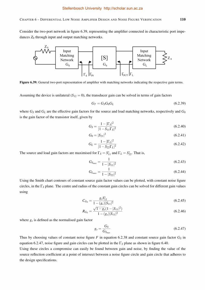
CHAPTER 6 – DIFFERENTIAL LOW NOISE AMPLIFIER DESIGN AND NOISE FIGURE VERIFICATION 110
Consider the two-port network in figure 6.39, representing the amplifier connected in characteristic port impe-
dances Z0 through input and output matching networks.
[S]
ΓOUT ΓL
Z 0
Z0
Input Matching Network
G
Input Matching Network
G
ΓINΓS
S G0 L
Figure 6.39: General two-port representation of amplifier with matching networks indicating the respective gain terms.
Assuming the device is unilateral (S12 = 0), the transducer gain can be solved in terms of gain factors
GT = GSG0GL (6.2.39)
where GS and GL are the effective gain factors for the source and load matching networks, respectively and G0
is the gain factor of the transistor itself, given by
GS =1−|ΓS|2
|1−S11ΓS|2(6.2.40)
G0 = |S21|2 (6.2.41)
GL =1−|ΓL|2
|1−S22ΓL|2(6.2.42)
The source and load gain factors are maximised for ΓS = S∗11 and ΓL = S∗22. That is,
GSmax =1
1−|S11|2(6.2.43)
GLmax =1
1−|S22|2(6.2.44)
Using the Smith chart contours of constant source gain factor values can be plotted, with constant noise figure
circles, in the ΓS plane. The centre and radius of the constant gain circles can be solved for different gain values
using
CGS =gsS∗11
1− (gs)|S11|2(6.2.45)
RGS =
√1−gs(1−|S11|2)1− (gs)|S11|2
(6.2.46)
where gs is defined as the normalised gain factor
gs =GS
GSmax
(6.2.47)
Thus by choosing values of constant noise figure F in equation 6.2.38 and constant source gain factor GS in
equation 6.2.47, noise figure and gain circles can be plotted in the ΓS plane as shown in figure 6.40.
Using these circles a compromise can easily be found between gain and noise, by finding the value of the
source reflection coefficient at a point of intersect between a noise figure circle and gain circle that adheres to
the design specifications.
Stellenbosch University http://scholar.sun.ac.za
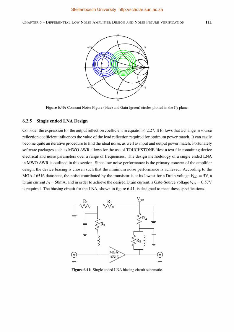
CHAPTER 6 – DIFFERENTIAL LOW NOISE AMPLIFIER DESIGN AND NOISE FIGURE VERIFICATION 111
0.33 1 30
-3j
-1j
-0.33j
0.33j
1j
3j
Figure 6.40: Constant Noise Figure (blue) and Gain (green) circles plotted in the ΓS plane.
6.2.5 Single ended LNA Design
Consider the expression for the output reflection coefficient in equation 6.2.27. It follows that a change in source
reflection coefficient influences the value of the load reflection required for optimum power match. It can easily
become quite an iterative procedure to find the ideal noise, as well as input and output power match. Fortunately
software packages such as MWO AWR allows for the use of TOUCHSTONE files: a text file containing device
electrical and noise parameters over a range of frequencies. The design methodology of a single ended LNA
in MWO AWR is outlined in this section. Since low noise performance is the primary concern of the amplifier
design, the device biasing is chosen such that the minimum noise performance is achieved. According to the
MGA-16516 datasheet, the noise contributed by the transistor is at its lowest for a Drain voltage VDD = 5V, a
Drain current ID = 50mA, and in order to achieve the desired Drain current, a Gate-Source voltage VGS = 0.57V
is required. The biasing circuit for the LNA, shown in figure 6.41, is designed to meet these specifications.
MGA 16516
VDD1R2R
3R4R
5R
Figure 6.41: Single ended LNA biasing circuit schematic.
Stellenbosch University http://scholar.sun.ac.za
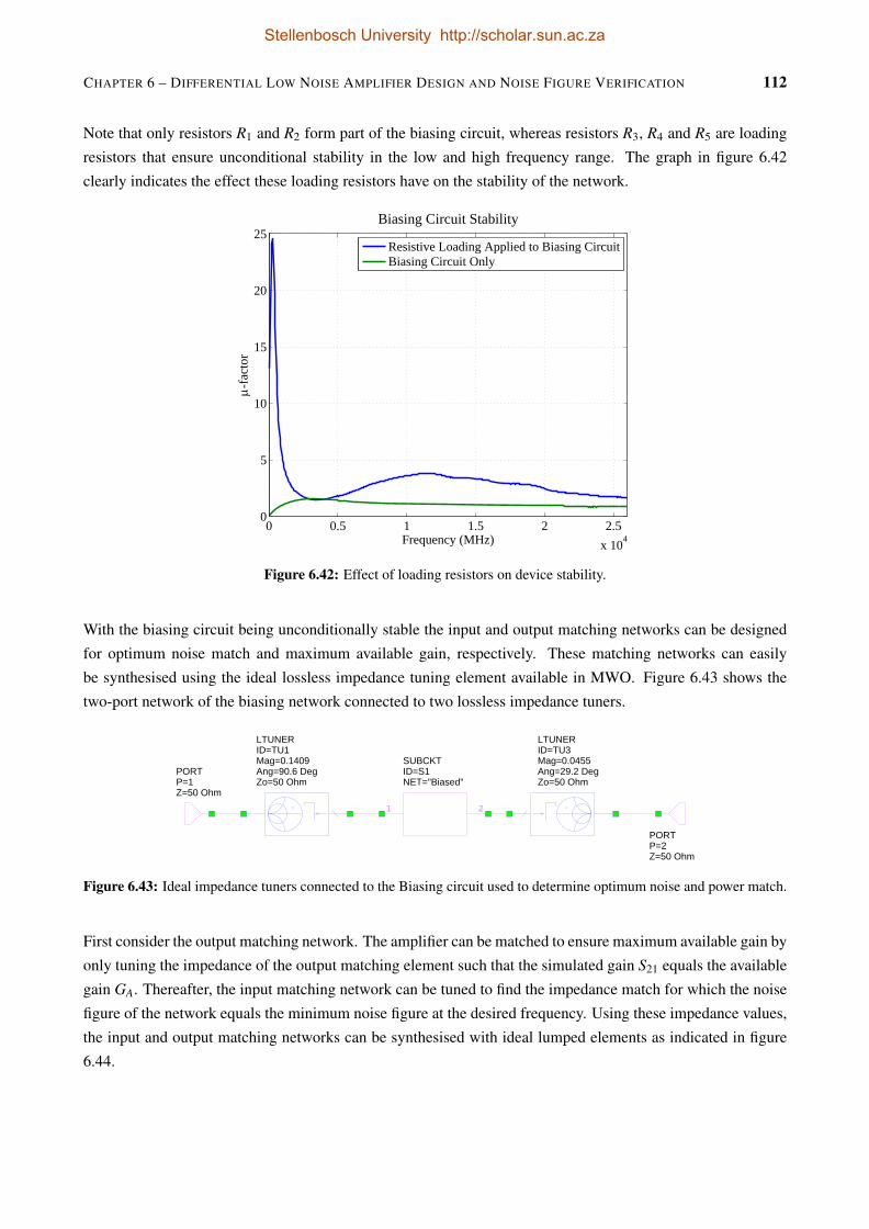
CHAPTER 6 – DIFFERENTIAL LOW NOISE AMPLIFIER DESIGN AND NOISE FIGURE VERIFICATION 112
Note that only resistors R1 and R2 form part of the biasing circuit, whereas resistors R3, R4 and R5 are loading
resistors that ensure unconditional stability in the low and high frequency range. The graph in figure 6.42
clearly indicates the effect these loading resistors have on the stability of the network.
0 0.5 1 1.5 2 2.5x 10⁴
0
5
10
15
20
25Biasing Circuit Stability
Frequency (MHz)
-fa
ctor
Resistive Loading Applied to Biasing CircuitBiasing Circuit Only
Figure 6.42: Effect of loading resistors on device stability.
With the biasing circuit being unconditionally stable the input and output matching networks can be designed
for optimum noise match and maximum available gain, respectively. These matching networks can easily
be synthesised using the ideal lossless impedance tuning element available in MWO. Figure 6.43 shows the
two-port network of the biasing network connected to two lossless impedance tuners.
LTUNERID=TU1Mag=0.1409Ang=90.6 DegZo=50 Ohm
LTUNERID=TU3Mag=0.0455Ang=29.2 DegZo=50 Ohm
Fo Fn. . .
ID=FSWP2Values= 1e9,1.
1 2
SUBCKTID=S1NET="Biased"
PORTP=1Z=50 Ohm
PORTP=2Z=50 Ohm
Figure 6.43: Ideal impedance tuners connected to the Biasing circuit used to determine optimum noise and power match.
First consider the output matching network. The amplifier can be matched to ensure maximum available gain by
only tuning the impedance of the output matching element such that the simulated gain S21 equals the available
gain GA. Thereafter, the input matching network can be tuned to find the impedance match for which the noise
figure of the network equals the minimum noise figure at the desired frequency. Using these impedance values,
the input and output matching networks can be synthesised with ideal lumped elements as indicated in figure
6.44.
Stellenbosch University http://scholar.sun.ac.za
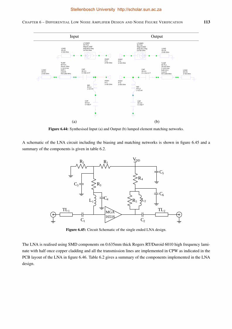
CHAPTER 6 – DIFFERENTIAL LOW NOISE AMPLIFIER DESIGN AND NOISE FIGURE VERIFICATION 113
Input Output
LOADID=Z1Z=50 Ohm
LTUNERID=TU1Mag=0.1409Ang=90.6 DegZo=50 Ohm
LOADID=Z2Z=50 Ohm
TLINPID=TL2Z0=61 OhmL=14.4 mmEeff=1Loss=0F0=1350 MHz
INDID=L1L=22 nH
CAPID=C1C=15e-12 F
CAPID=C2C=10p F
CAPID=C3C=1.2e-11 F
CAPID=C4C=10p F
INDID=L2L=22 nH
LOADID=Z3Z=50 Ohm
LOADID=Z4Z=50 Ohm
LTUNERID=TU2Mag=0.0455Ang=29.2 DegZo=50 Ohm
TLINPID=TL1Z0=50 OhmL=14.6 mmEeff=10.3Loss=0F0=1350 MHz
PORTP=1Z=50 Ohm
PORTP=2Z=50 Ohm
PORTP=3Z=50 Ohm
PORTP=4Z=50 Ohm
(a) (b)
Figure 6.44: Synthesised Input (a) and Output (b) lumped element matching networks.
A schematic of the LNA circuit including the biasing and matching networks is shown in figure 6.45 and a
summary of the components is given in table 6.2.
MGA 16516
VDD1R2R
3R4R
5R1L 2L
1C 2C
3C
4C
5C
6C
1TL 2TL
Figure 6.45: Circuit Schematic of the single ended LNA design.
The LNA is realised using SMD components on 0.635mm thick Rogers RT/Duroid 6010 high frequency lami-
nate with half once copper cladding and all the transmission lines are implemented in CPW as indicated in the
PCB layout of the LNA in figure 6.46. Table 6.2 gives a summary of the components implemented in the LNA
design.
Stellenbosch University http://scholar.sun.ac.za

CHAPTER 6 – DIFFERENTIAL LOW NOISE AMPLIFIER DESIGN AND NOISE FIGURE VERIFICATION 114
Figure 6.46: Layout of two matched single ended LNAs.
Table 6.2: Description of single ended LNA components
Designator Description Purpose
R1 10kΩ 0402 resistorVoltage divider for Gate biasing voltage
R2 1k3Ω 0402 resistor
R3, R4 10Ω 0402 resistor Loading resistor for Low frequency stability
R5 100Ω 0402 resistor Loading resistor for High frequency stability
L1, L2 22nH 0603 Inductor Input and Output Matching, RF Choke
C1 15pF 0402 Capacitor Input Matching, DC bolck
C2 12pF 0402 Capacitor Output Matching, DC block
C3 10nF 0402 CapacitorBypass CapacitorC4,6 10pF 0402 Capacitor
C5 1µF 0402 Capacitor
T L1 14.4mm 61Ω CPW Transmission line Input Matching, RF-input connection
T L2 14.6mm 50Ω CPW Transmission line RF-Output connection
To analyse the layout in figure 6.46 the circuit is simulated in MWO using coplanar EM-Quasi Static transmis-
sion line elements as well as measured S-parameter models for each of the lumped elements implemented in
the design. The simulated circuit schematic of the final LNA layout is shown in figure 6.49, and the graphs
in figures 6.47(a), 6.47(b) and 6.48 compare the measured Gain, Input and Output Reflection Coefficients as
well as the noise figure - measured using the setup depicted in figure 5.13 - of the LNA to that of the circuit
simulated in MWO.
Stellenbosch University http://scholar.sun.ac.za
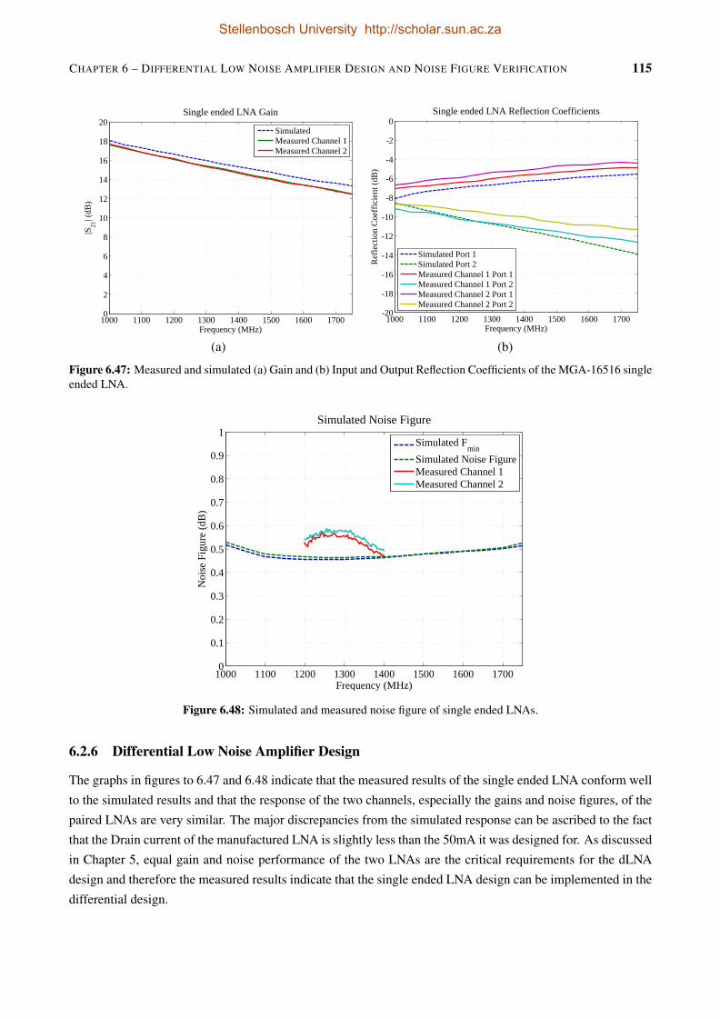
CHAPTER 6 – DIFFERENTIAL LOW NOISE AMPLIFIER DESIGN AND NOISE FIGURE VERIFICATION 115
1000 1100 1200 1300 1400 1500 1600 17000
2
4
6
8
10
12
14
16
18
20Single ended LNA Gain
Frequency (MHz)
|S21
| (dB
)
SimulatedMeasured Channel 1Measured Channel 2
1000 1100 1200 1300 1400 1500 1600 1700-20
-18
-16
-14
-12
-10
-8
-6
-4
-2
0Single ended LNA Reflection Coefficients
Frequency (MHz)
Ref
lect
ion
Coe
ffic
ient
(dB
)
Simulated Port 1Simulated Port 2Measured Channel 1 Port 1Measured Channel 1 Port 2Measured Channel 2 Port 1Measured Channel 2 Port 2
(a) (b)
Figure 6.47: Measured and simulated (a) Gain and (b) Input and Output Reflection Coefficients of the MGA-16516 singleended LNA.
1000 1100 1200 1300 1400 1500 1600 17000
0.1
0.2
0.3
0.4
0.5
0.6
0.7
0.8
0.9
1Simulated Noise Figure
Frequency (MHz)
Noi
se F
igur
e (d
B)
Simulated Fmin
Simulated Noise FigureMeasured Channel 1Measured Channel 2
Figure 6.48: Simulated and measured noise figure of single ended LNAs.
6.2.6 Differential Low Noise Amplifier Design
The graphs in figures to 6.47 and 6.48 indicate that the measured results of the single ended LNA conform well
to the simulated results and that the response of the two channels, especially the gains and noise figures, of the
paired LNAs are very similar. The major discrepancies from the simulated response can be ascribed to the fact
that the Drain current of the manufactured LNA is slightly less than the 50mA it was designed for. As discussed
in Chapter 5, equal gain and noise performance of the two LNAs are the critical requirements for the dLNA
design and therefore the measured results indicate that the single ended LNA design can be implemented in the
differential design.
Stellenbosch University http://scholar.sun.ac.za
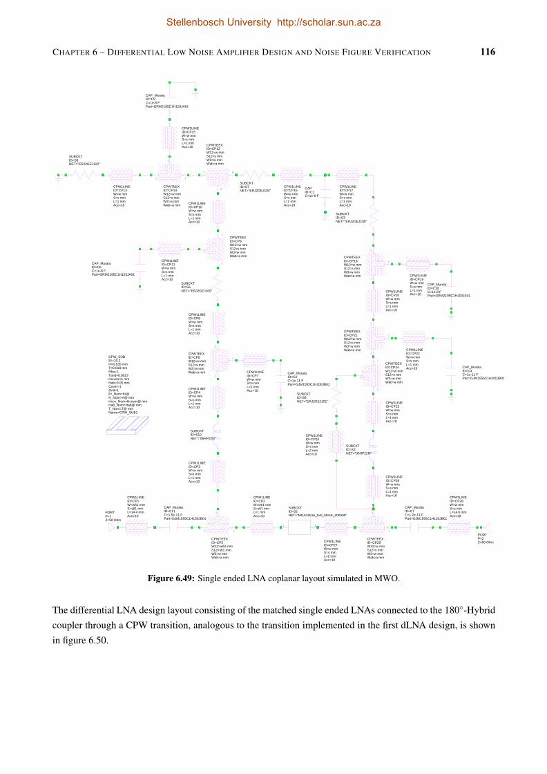
CHAPTER 6 – DIFFERENTIAL LOW NOISE AMPLIFIER DESIGN AND NOISE FIGURE VERIFICATION 116
CAP_MurataID=C6C=1e-8 FPart=GRM2195C1H103JA01
CAP_MurataID=C9C=1e-8 FPart=GRM2195C1H103JA01
CAP_MurataID=C10C=1e-8 FPart=GRM2195C1H103JA01
CAPID=C1C=1e-6 F
CPW_SUBEr=10.2H=0.635 mmT=0.018 mmRho=1Tand=0.0023Hcover=5 mmHab=0.05 mmCover=1Gnd=1Er_Nom=Er@H_Nom=H@ mmHcov_Nom=Hcover@ mmHab_Nom=Hab@ mmT_Nom=T@ mmName=CPW_SUB1
CPW1LINEID=CP1W=w61 mmS=s61 mmL=14.4 mmAcc=10
12
3
CPWTEEXID=CP5W12=w61 mmS12=s61 mmW3=w mmWab=a mm
CPW1LINEID=CP2W=w61 mmS=s61 mmL=1 mmAcc=10
CPW1LINEID=CP3W=w mmS=s mmL=1 mmAcc=10
CPW1LINEID=CP4W=w mmS=s mmL=1 mmAcc=10
1
2
3CPWTEEXID=CP6W12=w mmS12=s mmW3=w mmWab=a mm CPW1LINE
ID=CP7W=w mmS=s mmL=1 mmAcc=10
CPW1LINEID=CP8W=w mmS=s mmL=1 mmAcc=10
1
2
3
CPWTEEXID=CP9W12=w mmS12=s mmW3=w mmWab=a mm
CPW1LINEID=CP10W=w mmS=s mmL=1 mmAcc=10
CPW1LINEID=CP11W=w mmS=s mmL=1 mmAcc=10
1 2
3
CPWTEEXID=CP12W12=w mmS12=s mmW3=w mmWab=a mm
CPW1LINEID=CP13W=w mmS=s mmL=1 mmAcc=10
12
3
CPWTEEXID=CP14W12=w mmS12=s mmW3=w mmWab=a mm
CPW1LINEID=CP15W=w mmS=s mmL=1 mmAcc=10
CPW1LINEID=CP16W=w mmS=s mmL=1 mmAcc=10
CPW1LINEID=CP17W=w mmS=s mmL=1 mmAcc=10
1
2
3CPWTEEXID=CP18W12=w mmS12=s mmW3=w mmWab=a mm CPW1LINE
ID=CP19W=w mmS=s mmL=1 mmAcc=10
CPW1LINEID=CP20W=w mmS=s mmL=1 mmAcc=10
1
2
3CPWTEEXID=CP21W12=w mmS12=s mmW3=w mmWab=a mm CPW1LINE
ID=CP22W=w mmS=s mmL=1 mmAcc=10
CPW1LINEID=CP23W=w mmS=s mmL=1 mmAcc=10
1
2
3
CPWTEEXID=CP24W12=w mmS12=s mmW3=w mmWab=a mm
CPW1LINEID=CP25W=w mmS=s mmL=2 mmAcc=10
CPW1LINEID=CP26W=w mmS=s mmL=1 mmAcc=10
CPW1LINEID=CP27W=w mmS=s mmL=2 mmAcc=10
CPW1LINEID=CP28W=w mmS=s mmL=14.6 mmAcc=10
12
3
CPWTEEXID=CP29W12=w mmS12=s mmW3=w mmWab=a mm
CAP_MurataID=C7C=1.2e-11 FPart=GJM1555C1H120JB01
CAP_MurataID=C2C=1e-11 FPart=GJM1555C1H100JB01
CAP_MurataID=C3C=1e-11 FPart=GJM1555C1H100JB01
CAP_MurataID=C11C=1.5e-11 FPart=GJM1555C1H150JB01
Fo Fn. . .
SWPFRQID=FSWP2Values= 1e9,1.1e9,1.2e9,1.35e9,1.4e9,1.5e9,1.6e9,1.7e9,1.75e9
1 2
SUBCKTID=S1NET="MGA16516_5v0_50mA_200509"
SUBCKTID=S5NET="ERJ2GEJ100"
SUBCKTID=S3NET="ERJ2GEJ100"
SUBCKTID=S6NET="ERJ2GEJ101"
SUBCKTID=S7NET="ERJ2GEJ104"
SUBCKTID=S8NET="ERJ2GEJ122"
SUBCKTID=S2NET="06HP22N"
SUBCKTID=S10NET="06HP22N"
PORTP=1Z=50 Ohm
PORTP=2Z=50 Ohm
w10=0.508s=0.254a=0.4
w=0.39w61=0.3s61=0.4
Figure 6.49: Single ended LNA coplanar layout simulated in MWO.
The differential LNA design layout consisting of the matched single ended LNAs connected to the 180-Hybrid
coupler through a CPW transition, analogous to the transition implemented in the first dLNA design, is shown
in figure 6.50.
Stellenbosch University http://scholar.sun.ac.za

CHAPTER 6 – DIFFERENTIAL LOW NOISE AMPLIFIER DESIGN AND NOISE FIGURE VERIFICATION 117CST MICROWAVE STUDIO *** Educational Version *** 09/16/2011 - 02:35
File: C:\Users\David\Documents\CST 2010\TEMP\Temp\DE1\Untitled_0.cst
Figure 6.50: PCB layout of Differential Low Noise Amplifier.
Using the simulated S-parameters of the 180-Hybrid coupler and the CPW transition the response of the
differential LNA is analysed in MWO AWR. The simulated schematic network is similar to the schematic used
for the first dLNA design shown in figure 6.31, where the ’Single Ended LNA’ two-port network contains the
S- and noise parameters of the single ended LNA design depicted in figure 6.49. Note that the length of the
output transmission line segment has been extended to 50.4mm to correspond to the layout depicted in figure
6.50.
1000 1100 1200 1300 1400 1500 1600 17000
5
10
15
20Differential Gain Compared to Single Ended Gain
Frequency (MHz)
dB
MeasuredSimulatedSingle Ended LNA
1000 1100 1200 1300 1400 1500 1600 17000
10
20
30
40
50
Common Mode Rejection Ratio
Frequency (MHz)
CM
RR
(dB
)
Measured CMRRSimulated CMRRSimulated Coupler Isolation
(a) (b)
Figure 6.51: Measured and simulated (a) Gains and (b) CMRR of the MGA-16516 differential LNA.
Stellenbosch University http://scholar.sun.ac.za

CHAPTER 6 – DIFFERENTIAL LOW NOISE AMPLIFIER DESIGN AND NOISE FIGURE VERIFICATION 118
Applying equations 6.2.2 to 6.2.6 to the scattering parameters of the measured and simulated three-port diffe-
rential LNA, the mixed-mode performance of the dLNA can be investigated. Starting with the device gain, the
graph in figure 6.51(a) shows the simulated and measured differential gains as calculated using equation 6.2.2,
and compares these gain values to that of the single ended LNA design. The graph indicates that although there
is approximately a 3 dB loss in gain along each of the respective signal paths, when considering a differential
excitation the differential gain of the dLNA nearly equals that of its constituent single ended LNAs.
The simulated and measured CMRR of the dLNA is compared in the graph in figure 6.51(b). Included in the
graph is the isolation between the sum and difference ports of the 180-Hybrid coupler and comparing the
simulated isolation of the coupler to the CMRR clearly indicates that the isolation of the coupler determines the
CMRR of this dLNA design topology.
1000 1100 1200 1300 1400 1500 1600 1700-15
-10
-5
0Differential Input Reflection Coefficient
Frequency (MHz)
Ref
lect
ion
Coe
ffic
ient
(dB
)
Measured Differential LNASimulated Differential LNASingle Ended LNA
1000 1100 1200 1300 1400 1500 1600 1700-25
-20
-15
-10
-5
0Output Reflection Coefficient of dLNA
Frequency (MHz)
Ref
lect
ion
Coe
ffic
ient
(dB
)
Measured Differential LNASimulated Differential LNASingle Ended LNA
(a) (b)
Figure 6.52: Simulated (a) Input and (b) Output Reflection Coefficients of Differential LNA.
Figure 6.52 shows the simulated and measured differential input reflection coefficients as well as the reflection
coefficient simulated at the single ended output port. The graph shows that the input reflection for a differential
input port is similar to that of each of the constituent single ended input ports. Furthermore, it can be seen that
the cascaded connection of the 180-Hybrid coupler with the single ended LNA causes a slight degradation in
the output reflection of the dLNA when comparing it to that of the single ended LNA.
The amplitude and phase difference between the signals along the two respective signal paths is shown in the
graph in figure 6.53. As expected from the simulated response of the 180-Hybrid coupler, figures 6.20 and
6.21, the amplitude of the gains along the two signal paths of the dLNA differ by less than 1 dB, and the phase
difference deviates from 180 by less than 5 across the band.
Stellenbosch University http://scholar.sun.ac.za
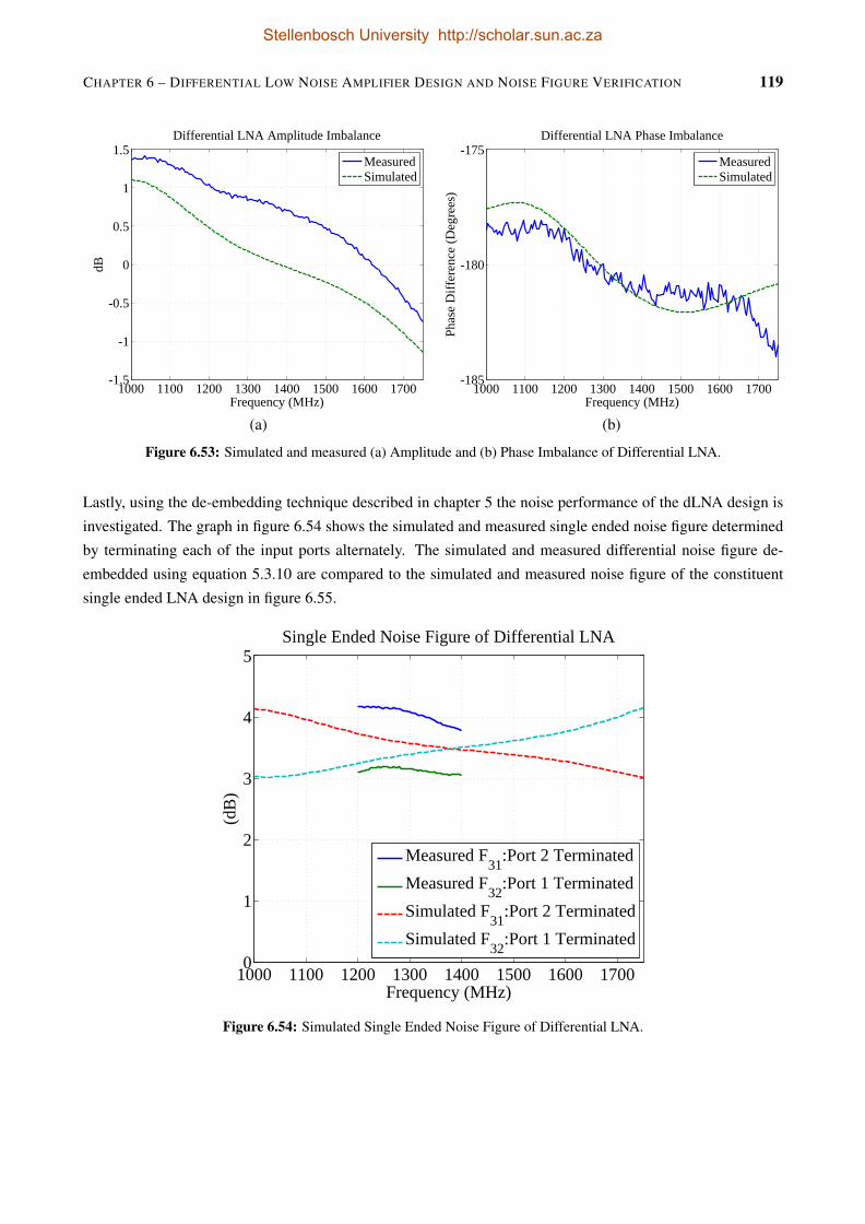
CHAPTER 6 – DIFFERENTIAL LOW NOISE AMPLIFIER DESIGN AND NOISE FIGURE VERIFICATION 119
1000 1100 1200 1300 1400 1500 1600 1700-1.5
-1
-0.5
0
0.5
1
1.5Differential LNA Amplitude Imbalance
Frequency (MHz)
dB
MeasuredSimulated
1000 1100 1200 1300 1400 1500 1600 1700-185
-180
-175Differential LNA Phase Imbalance
Frequency (MHz)
Phas
e D
iffer
ence
(Deg
rees
)
MeasuredSimulated
(a) (b)
Figure 6.53: Simulated and measured (a) Amplitude and (b) Phase Imbalance of Differential LNA.
Lastly, using the de-embedding technique described in chapter 5 the noise performance of the dLNA design is
investigated. The graph in figure 6.54 shows the simulated and measured single ended noise figure determined
by terminating each of the input ports alternately. The simulated and measured differential noise figure de-
embedded using equation 5.3.10 are compared to the simulated and measured noise figure of the constituent
single ended LNA design in figure 6.55.
1000 1100 1200 1300 1400 1500 1600 17000
1
2
3
4
5Single Ended Noise Figure of Differential LNA
Frequency (MHz)
(dB
)
Measured F31:Port 2 TerminatedMeasured F32:Port 1 TerminatedSimulated F31:Port 2 TerminatedSimulated F32:Port 1 Terminated
Figure 6.54: Simulated Single Ended Noise Figure of Differential LNA.
Stellenbosch University http://scholar.sun.ac.za
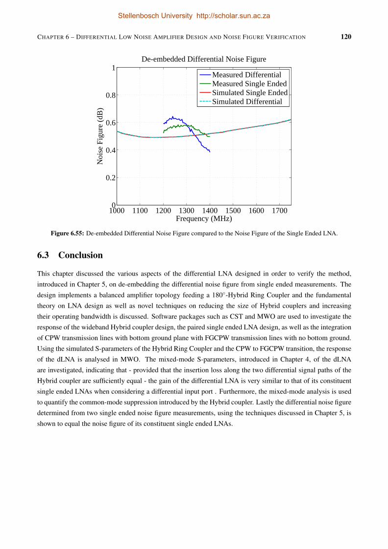
CHAPTER 6 – DIFFERENTIAL LOW NOISE AMPLIFIER DESIGN AND NOISE FIGURE VERIFICATION 120
1000 1100 1200 1300 1400 1500 1600 17000
0.2
0.4
0.6
0.8
1De-embedded Differential Noise Figure
Frequency (MHz)
Noi
se F
igur
e (d
B)
Measured DifferentialMeasured Single EndedSimulated Single EndedSimulated Differential
Figure 6.55: De-embedded Differential Noise Figure compared to the Noise Figure of the Single Ended LNA.
6.3 Conclusion
This chapter discussed the various aspects of the differential LNA designed in order to verify the method,
introduced in Chapter 5, on de-embedding the differential noise figure from single ended measurements. The
design implements a balanced amplifier topology feeding a 180-Hybrid Ring Coupler and the fundamental
theory on LNA design as well as novel techniques on reducing the size of Hybrid couplers and increasing
their operating bandwidth is discussed. Software packages such as CST and MWO are used to investigate the
response of the wideband Hybrid coupler design, the paired single ended LNA design, as well as the integration
of CPW transmission lines with bottom ground plane with FGCPW transmission lines with no bottom ground.
Using the simulated S-parameters of the Hybrid Ring Coupler and the CPW to FGCPW transition, the response
of the dLNA is analysed in MWO. The mixed-mode S-parameters, introduced in Chapter 4, of the dLNA
are investigated, indicating that - provided that the insertion loss along the two differential signal paths of the
Hybrid coupler are sufficiently equal - the gain of the differential LNA is very similar to that of its constituent
single ended LNAs when considering a differential input port . Furthermore, the mixed-mode analysis is used
to quantify the common-mode suppression introduced by the Hybrid coupler. Lastly the differential noise figure
determined from two single ended noise figure measurements, using the techniques discussed in Chapter 5, is
shown to equal the noise figure of its constituent single ended LNAs.
Stellenbosch University http://scholar.sun.ac.za
Chapter 7
Conclusion
As stated in the introduction, the characterisation of differential Low Noise Amplifiers (LNAs) is not a trivial
task. This thesis aimed to provide the reader with the necessary background regarding the noise performance
of microwave circuits. This entailed a brief history of the discovery of noise in electronic circuits and a detailed
description of the physical origin of the two predominant sources of noise namely Shot Noise and Thermal
Noise. Knowing the physical origin of these sources of noise, the familiar equivalent small signal models of
two widely used active devices - Bipolar Junction Transistors (BJTs) and FET - were adapted to include their
associated noise generators. Various authors have published work on the noise and signal performance of these
equivalent noise models, each ascribing unique noise generators to the existing small signal models. Chapter 2
introduced two noise models for BJTs, one considering correlated noise sources in section 2.3.2.2 and another
assuming uncorrelated noise generators in section 2.3.2.1. These models were compared to one another and
the effect of neglecting the correlation between sources was made clear. Noise models developed for Field
Effect Transistors (FETs) were introduced and the model proposed by Pospieszalski was validated in section
2.4.2. Including the noise generators in equivalent small signal models can quickly complicate the analysis of
even the simplest circuits. Therefore methods were introduced by which two-port devices can be represented
by a noiseless two-port network with two equivalent noise generators connected to the external ports. By re-
presenting a noisy two-port in this manner the noise and signal performance of the two-port network can be
described by an equivalent electrical matrix and its corresponding noise matrix, referred to as the correlation
matrix, introduced in chapter 3. Correlation matrices for three of the most common two-port electrical repre-
sentations were introduced, namely the Admittance, Impedance and Chain representations and the methods for
transforming between various representation were discussed - significantly simplifying two-port noise analy-
sis. The real importance of the correlation matrix was made clear by the elegant relationship derived between
the chain representation and the noise parameters of a linear two-port device. This relation together with the
transformation matrices provided the means by which the noise performance of multi-port networks could be
derived. Chapter 4 introduced the concept of differential and common-mode signals, referred to as mixed-mode
signals, that can propagate in multi-port networks. Using the analysis of coupled transmission lines a simple re-
lation between the mixed-mode and general scattering parameters was derived. It was later shown that the same
analysis applies to the noise within multi-port networks, when the mixed-mode correlation matrix was derived
in section 6.2.1 making it possible to completely characterise the noise and signal performance of differential
microwave networks.
121
Stellenbosch University http://scholar.sun.ac.za
CHAPTER 7 – CONCLUSION 122
Chapter 5 introduced a number of noise figure measurement techniques for both two-port and differential de-
vices and investigated the effect various proposed measurement improvement techniques have on the calibration
of an N8975A NFA when using a high ENR noise source. This investigation illustrated the uncertainty any mis-
match between the noise source and DUT, or the DUT and the NFA, can introduce when performing low noise
figure measurements and it was shown that circulators at the input and the output of the DUT provided the most
reliable measurements. Furthermore, based on the de-embedding technique proposed by Belostotski an expres-
sion was derived by which the differential noise figure of a three-port device can be de-embedded from two
single ended noise figure measurements and it was shown that the differential noise figure of a dLNA equals
that of its constituent single ended LNAs. To verify these expressions two differential LNAs were designed,
manufactured and measured. The LNA designs discussed in chapter 6 illustrated the viability of implementing
a differential LNA using a balanced amplifier topology feeding a 180-Hybrid coupler and showed that, provi-
ded that the insertion loss along the two differential signal paths of the coupler are near equal, the differential
gain of the dLNA equals the single ended gain of its constituent single ended LNAs. More importantly, the two
designs illustrate the validity of using equation 5.3.10 to de-embed the differential noise figure from two single
ended measurements.
It seems as though, despite the lack of definitive definitions and measurement procedures, the signal and noise
performance of an L-band differential LNA can be accurately characterised using the methods outlined in this
thesis. One thing is certain, the characterisation of differential LNAs at the higher frequency range of the
MeerKAT receivers - 8 to 14.5 GHz - will bring forth exciting challenges. The author hopes that the work
presented in this thesis would aid in the pursuit of finding alternative techniques by which the nuisance that is
noise can be better prevented, cured or endured.
Stellenbosch University http://scholar.sun.ac.za
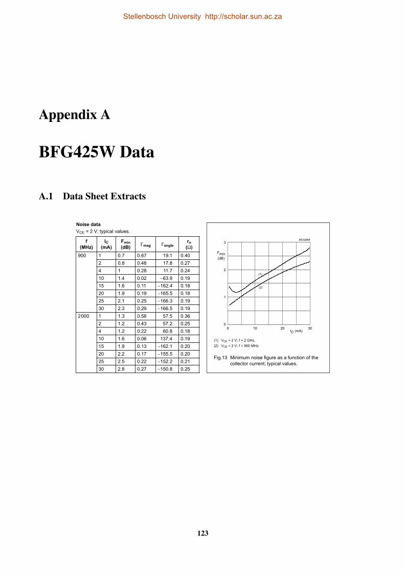
Appendix A
BFG425W Data
A.1 Data Sheet Extracts
⊃∫
π
⌠π
⌠π
⌠π
π
π
π
π
∧ ∧
⊃
⌠
⌠
⌠
⌠
⌠
⌠
⌠
⌠
⌠
123
Stellenbosch University http://scholar.sun.ac.za
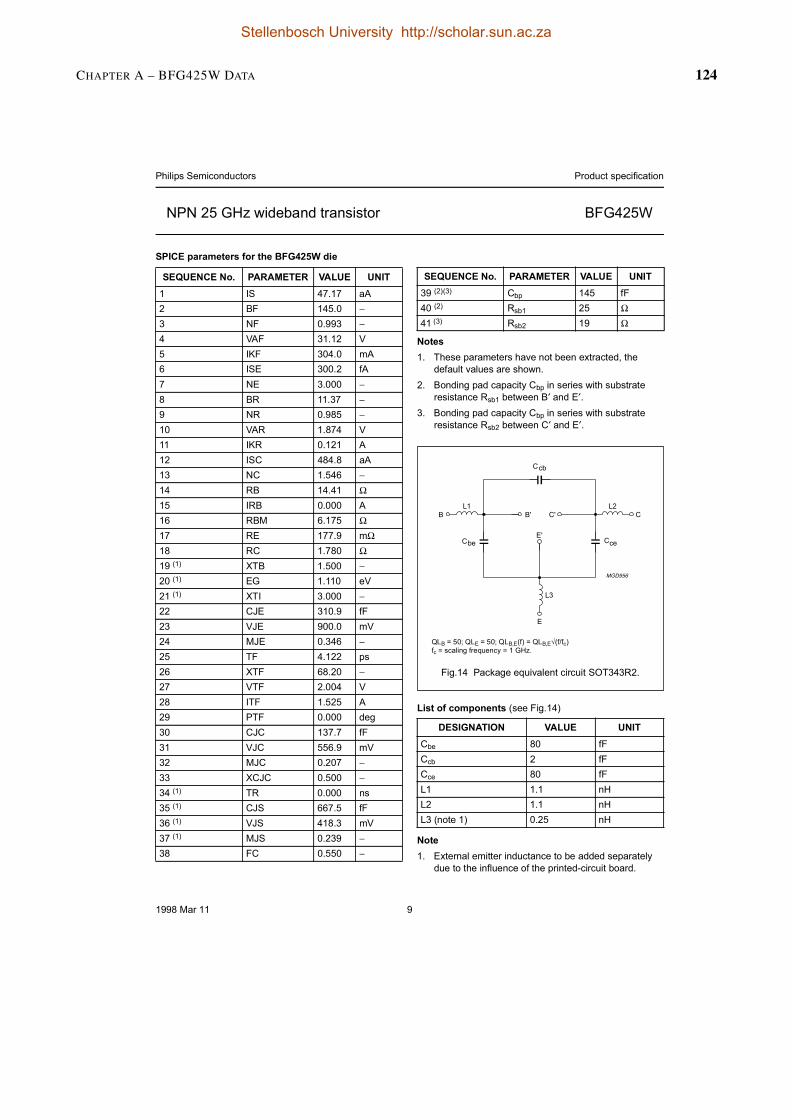
CHAPTER A – BFG425W DATA 124
!"#
! "# !
$ "%&% '
! "&(
) ! (&)
" *'! )& *
$+! )("&( '
, $- )((& .'
% - )&(((
/ &)%
/ (&
( *'/ &%" *
$+/ (& '
$0 ""& '
) 0 &",
" / "&"
$/ (&((( '
, / ,&%
% /- %%&
/0 &%(
12 34 &((
( 12 - &( *
12 34$ )&(((
05- )(& .!
) *5- ((&( *
" 5- (&)",
4! "&
, 34! ,&(
% *4! &((" *
$4! & '
4! (&((( 6
)( 050 )%&% .!
) *50 ,& *
) 50 (&(%
)) 3050 (&((
)" 12 4/ (&(((
) 12 05 ,,%& .!
), 12 *5 "&) *
)% 12 5 (&)
) !0 (&(
& 4 7 89
. 7 &
& 6 : 0
/ -&
)& 6 : 0
/ 0 -&
# $%% 1 !6&"2
& -8 :
. . ; &
) 121)2 0 " .!
"( 12 /
" 1)2 /
&!' "# !
0 ( .!
0 .!
0 ( .!
< &
< &
<) 1 2 (&
! "# !
=< > (? =<- > (? =< 9-1.2 > =< [email protected]. > 6 .A: > &
!6&" B6 A7 C4)")/&
Stellenbosch University http://scholar.sun.ac.za

CHAPTER A – BFG425W DATA 125
A.2 Touchstone Data
BFG425W! Filename: 25bfg425.001! BFG425W Field C1! V1=8.298E-001V,V2=2.000E+000V, I1=6.614E-005A, I2=5.000E-003A# GHz S MA R 50! S11 S21 S12 S22!Freq(GHz) Mag Ang Mag Ang Mag Ang Mag Ang 1.000 0.567 -81.910 10.277 113.589 0.044 47.988 0.720 -44.028 1.100 0.543 -88.354 9.760 108.883 0.047 45.593 0.691 -46.856 1.200 0.521 -94.563 9.272 104.380 0.049 43.540 0.663 -49.519 1.300 0.500 -100.541 8.816 100.164 0.051 41.682 0.637 -51.993 1.400 0.480 -106.351 8.397 96.144 0.053 40.039 0.612 -54.269 1.500 0.463 -112.066 7.999 92.308 0.054 38.567 0.590 -56.428 1.600 0.447 -117.771 7.635 88.594 0.056 37.199 0.569 -58.521 1.700 0.433 -123.099 7.289 85.040 0.057 35.994 0.549 -60.543 1.800 0.421 -128.336 6.969 81.649 0.059 34.871 0.530 -62.480! DEEMBEDDED NOISE DATA!FREQUENCY FMIN GAMMA OPT Rn! (GHz) (dB) Mag Ang (NORMALIZED)
1 0.9958 0.4683 10.638 0.34 1.1 1.0204 0.4579 11.795 0.34 1.2 1.0464 0.4471 12.979 0.34 1.3 1.0737 0.4359 14.194 0.34 1.4 1.1022 0.4245 15.444 0.34 1.5 1.1316 0.4128 16.731 0.34 1.6 1.1619 0.4011 18.059 0.34 1.7 1.193 0.3893 19.431 0.34 1.8 1.2247 0.3776 20.852 0.34
Page 1
Stellenbosch University http://scholar.sun.ac.za
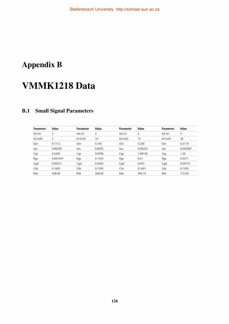
Appendix B
VMMK1218 Data
B.1 Small Signal Parameters
8
Small Signal Model Parameters
Parameter Value Parameter Value Parameter Value Parameter ValueVd (V) 1.5 Vd (V) 1.5 Vd (V) 1.5 Vd (V) 1.5
Id (mA) 5 Id (mA) 10 Id (mA) 15 Id (mA) 20
Gm 0.1162 Gm 0.2019 Gm 0.2374 Gm 0.3249
tau 0.00188 tau 0.002388 tau 0.002702 tau 0.00271
Cgs 0.5131 Cgs 0.6732 Cgs 0.8077 Cgs 0.929
Rgs 0.2126 Rgs 0.02638 Rgs 0.02069 Rgs 0.0304
Cgd 0.06932 Cgd 0.06226 Cgd 0.0777 Cgd 0.07133
Cds 0.1587 Cds 0.1574 Cds 0.1606 Cds 0.1597
Rds 334.70 Rds 187.10 Rds 154.10 Rds 123.80
Parameter Value Parameter Value Parameter Value Parameter ValueVd (V) 2 Vd (V) 2 Vd (V) 2 Vd (V) 2
Id (mA) 5 Id (mA) 10 Id (mA) 15 Id (mA) 20
Gm 0.1159 Gm 0.1992 Gm 0.1992 Gm 0.3199
tau 0.002146 tau 0.002394 tau 0.002394 tau 0.00257
Cgs 0.5661 Cgs 0.7445 Cgs 0.7445 Cgs 1.04381
Rgs 0.2293 Rgs 0.01936 Rgs 0.01936 Rgs 0.01756
Cgd 0.07976 Cgd 0.0726 Cgd 0.0726 Cgd 0.0606
Cds 0.1631 Cds 0.16078 Cds 0.16078 Cds 0.1607
Rds 357.50 Rds 222.00 Rds 222.00 Rds 141.70
Parameter Value Parameter Value Parameter Value Parameter ValueVd (V) 3 Vd (V) 3 Vd (V) 3 Vd (V) 3
Id (mA) 5 Id (mA) 10 Id (mA) 15 Id (mA) 20
Gm 0.1112 Gm 0.193 Gm 0.258 Gm 0.3119
tau 0.00249 tau 0.0025 tau 0.00252 tau 0.002487
Cgs 0.6365 Cgs 0.8786 Cgs 1.08192 Cgs 1.26
Rgs 0.007447 Rgs 0.1353 Rgs 0.01 Rgs 0.0271
Cgd 0.06521 Cgd 0.0582 Cgd 0.053 Cgd 0.04772
Cds 0.1603 Cds 0.1595 Cds 0.1601 Cds 0.1595
Rds 438.90 Rds 260.60 Rds 209.10 Rds 172.90
Parameter Value Parameter Value Parameter Value Parameter ValueVd (V) 4 Vd (V) 4 Vd (V) 4 Vd (V) 4
Id (mA) 5 Id (mA) 10 Id (mA) 15 Id (mA) 20
Gm 0.1088 Gm 0.1909 Gm 0.2509 Gm 0.3053
tau 0.00264 tau 0.002635 tau 0.002613 tau 0.00261
Cgs 0.6765 Cgs 0.9774 Cgs 1.203 Cgs 1.412
Rgs 0.00818 Rgs 0.1478 Rgs 0.01263 Rgs 0.02727
Cgd 0.05762 Cgd 0.05065 Cgd 0.04603 Cgd 0.04153
Cds 0.1565 Cds 0.1573 Cds 0.1574 Cds 0.1579
Rds 564.30 Rds 312.10 Rds 242.20 Rds 200.30
126
Stellenbosch University http://scholar.sun.ac.za

CHAPTER B – VMMK1218 DATA 127
B.2 Scattering and Noise Parameters
7
VMMK-1218 Typical Scattering Parameters and Noise Parameters, TA=25°C, Vds=3V, Ids=20mA [1]
Freq S11 S21 S12 S22 MSG/MAG
GHz Mag. Ang. dB Mag. Ang. Mag. Ang. Mag. Ang. dB
2 0.90 -78.41 20.88 11.07 129.30 0.05 44.78 0.59 -45.41 29.71
3 0.85 -106.62 19.27 9.19 111.50 0.06 29.68 0.50 -61.56 26.11
4 0.82 -129.23 17.67 7.65 96.89 0.07 17.84 0.43 -74.78 23.29
5 0.80 -146.90 16.21 6.47 84.82 0.07 8.51 0.38 -85.37 21.29
6 0.79 -161.57 14.90 5.56 74.28 0.07 0.60 0.35 -94.96 19.70
7 0.78 -173.94 13.71 4.85 64.67 0.07 -6.02 0.32 -103.77 18.32
8 0.78 175.49 12.63 4.28 55.85 0.07 -12.05 0.31 -112.18 17.17
9 0.78 166.35 11.62 3.81 47.60 0.07 -17.59 0.30 -120.67 16.14
10 0.78 158.10 10.70 3.43 39.76 0.07 -22.09 0.29 -128.21 15.23
11 0.79 150.68 9.87 3.11 32.39 0.07 -26.72 0.29 -135.58 14.44
12 0.79 143.93 9.09 2.85 25.16 0.07 -30.99 0.30 -142.88 13.76
13 0.79 137.47 8.38 2.62 18.21 0.07 -34.81 0.31 -149.97 13.11
14 0.80 131.33 7.71 2.43 11.48 0.06 -38.24 0.31 -156.46 12.54
15 0.80 125.54 7.11 2.27 4.87 0.06 -40.97 0.33 -162.44 12.02
16 0.80 119.64 6.53 2.12 -1.87 0.06 -44.55 0.34 -168.20 11.55
17 0.81 113.80 6.00 2.00 -8.47 0.06 -46.49 0.35 -174.07 11.14
18 0.81 108.24 5.48 1.88 -14.69 0.06 -49.45 0.36 -179.63 10.72
Typical Noise Parameters
Freq Fmin Г opt Г opt Rn/50 Ga
GHz dB Mag. Ang. dB
2 0.16 0.72 30.40 0.10 20.29
3 0.23 0.62 45.50 0.10 18.62
4 0.30 0.53 60.30 0.09 17.08
5 0.37 0.45 74.80 0.08 15.69
6 0.44 0.39 89.10 0.08 14.44
7 0.50 0.34 103.00 0.07 13.34
8 0.57 0.30 116.70 0.07 12.37
9 0.64 0.28 130.10 0.07 11.55
10 0.71 0.27 143.20 0.06 10.87
11 0.77 0.27 156.00 0.06 10.34
12 0.84 0.29 168.60 0.06 9.95
13 0.91 0.31 -179.20 0.06 9.70
14 0.98 0.36 -167.20 0.06 9.59
15 1.05 0.41 -155.50 0.06 9.63
16 1.11 0.48 -144.10 0.07 9.81
17 1.18 0.56 -132.90 0.08 10.13
Note: 1. S-parameters are measured in 50 Ohm test environment.
Figure 14. MSG/MAG and S21 vs. Frequency at 3V 20 mA
0.00
10.00
20.00
30.00
40.00
0 5 10 15 20FREQUENCY GHz
MSG/MAG
and S2
1 (dB
)
MSG/MAGS21
Stellenbosch University http://scholar.sun.ac.za
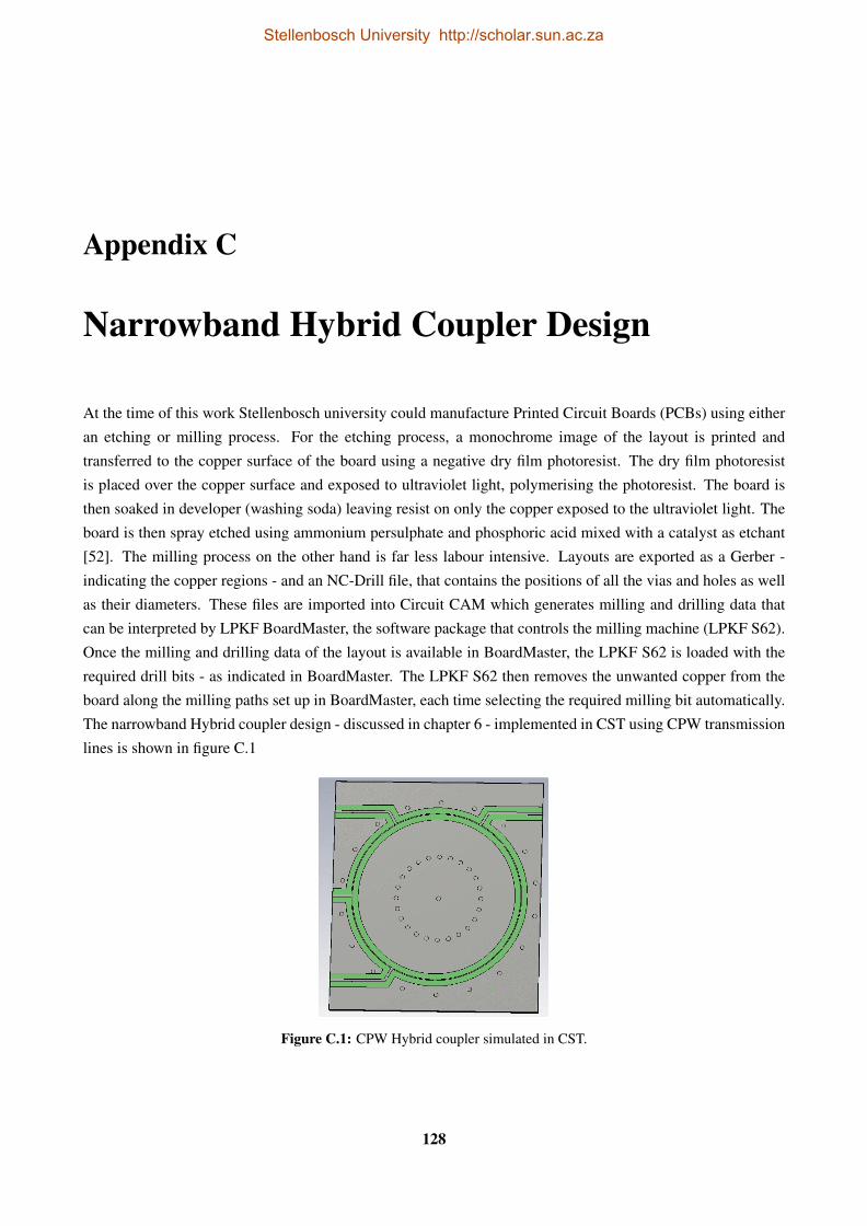
Appendix C
Narrowband Hybrid Coupler Design
At the time of this work Stellenbosch university could manufacture Printed Circuit Boards (PCBs) using either
an etching or milling process. For the etching process, a monochrome image of the layout is printed and
transferred to the copper surface of the board using a negative dry film photoresist. The dry film photoresist
is placed over the copper surface and exposed to ultraviolet light, polymerising the photoresist. The board is
then soaked in developer (washing soda) leaving resist on only the copper exposed to the ultraviolet light. The
board is then spray etched using ammonium persulphate and phosphoric acid mixed with a catalyst as etchant
[52]. The milling process on the other hand is far less labour intensive. Layouts are exported as a Gerber -
indicating the copper regions - and an NC-Drill file, that contains the positions of all the vias and holes as well
as their diameters. These files are imported into Circuit CAM which generates milling and drilling data that
can be interpreted by LPKF BoardMaster, the software package that controls the milling machine (LPKF S62).
Once the milling and drilling data of the layout is available in BoardMaster, the LPKF S62 is loaded with the
required drill bits - as indicated in BoardMaster. The LPKF S62 then removes the unwanted copper from the
board along the milling paths set up in BoardMaster, each time selecting the required milling bit automatically.
The narrowband Hybrid coupler design - discussed in chapter 6 - implemented in CST using CPW transmission
lines is shown in figure C.1
Figure C.1: CPW Hybrid coupler simulated in CST.
128
Stellenbosch University http://scholar.sun.ac.za
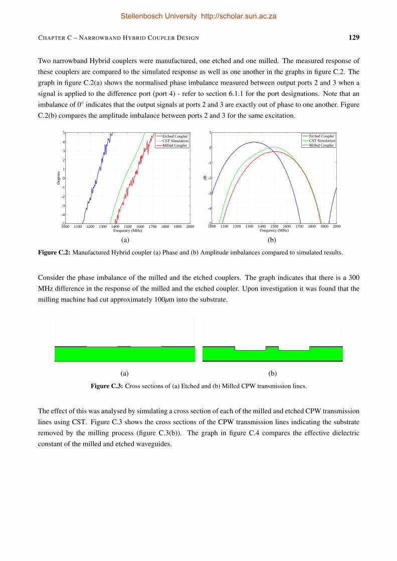
CHAPTER C – NARROWBAND HYBRID COUPLER DESIGN 129
Two narrowband Hybrid couplers were manufactured, one etched and one milled. The measured response of
these couplers are compared to the simulated response as well as one another in the graphs in figure C.2. The
graph in figure C.2(a) shows the normalised phase imbalance measured between output ports 2 and 3 when a
signal is applied to the difference port (port 4) - refer to section 6.1.1 for the port designations. Note that an
imbalance of 0 indicates that the output signals at ports 2 and 3 are exactly out of phase to one another. Figure
C.2(b) compares the amplitude imbalance between ports 2 and 3 for the same excitation.
1000 1100 1200 1300 1400 1500 1600 1700 1800 1900 2000-5
-4
-3
-2
-1
0
1
2
3
4
5
Frequency (MHz)
Deg
rees
Etched CouplerCST SimulationMilled Coupler
1000 1100 1200 1300 1400 1500 1600 1700 1800 1900 2000-5
-4
-3
-2
-1
0
1
Frequency (MHz)
dB
Etched CouplerCST SimulationMilled Coupler
(a) (b)
Figure C.2: Manufactured Hybrid coupler (a) Phase and (b) Amplitude imbalances compared to simulated results.
Consider the phase imbalance of the milled and the etched couplers. The graph indicates that there is a 300
MHz difference in the response of the milled and the etched coupler. Upon investigation it was found that the
milling machine had cut approximately 100µm into the substrate.
(a) (b)
Figure C.3: Cross sections of (a) Etched and (b) Milled CPW transmission lines.
The effect of this was analysed by simulating a cross section of each of the milled and etched CPW transmission
lines using CST. Figure C.3 shows the cross sections of the CPW transmission lines indicating the substrate
removed by the milling process (figure C.3(b)). The graph in figure C.4 compares the effective dielectric
constant of the milled and etched waveguides.
Stellenbosch University http://scholar.sun.ac.za
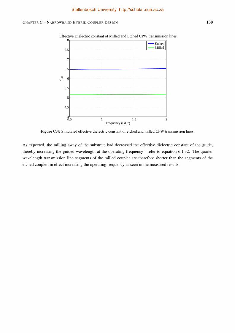
CHAPTER C – NARROWBAND HYBRID COUPLER DESIGN 130
0.5 1 1.5 24
4.5
5
5.5
6
6.5
7
7.5
8Effective Dielectric constant of Milled and Etched CPW transmission lines
Frequency (GHz)
eff
EtchedMilled
Figure C.4: Simulated effective dielectric constant of etched and milled CPW transmission lines.
As expected, the milling away of the substrate had decreased the effective dielectric constant of the guide,
thereby increasing the guided wavelength at the operating frequency - refer to equation 6.1.32. The quarter
wavelength transmission line segments of the milled coupler are therefore shorter than the segments of the
etched coupler, in effect increasing the operating frequency as seen in the measured results.
Stellenbosch University http://scholar.sun.ac.za
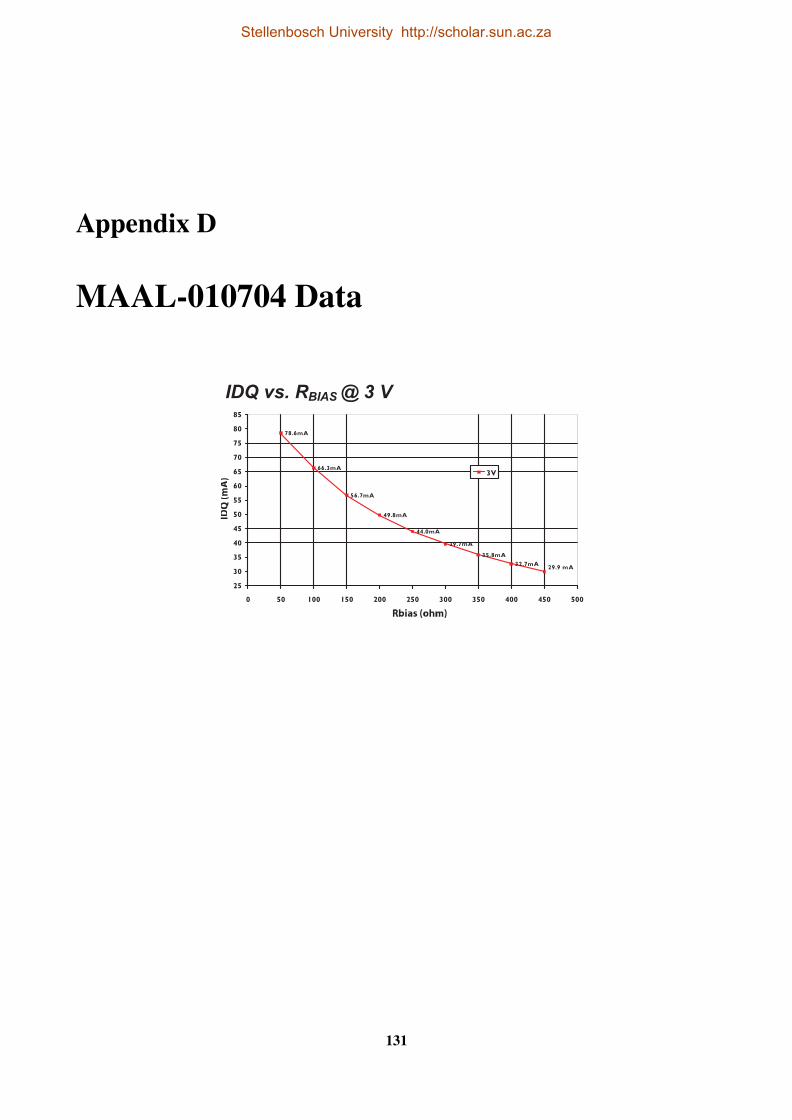
Appendix D
MAAL-010704 Data
• North America Tel: 800.366.2266 • Europe Tel: +353.21.244.6400
• India Tel: +91.80.43537383 • China Tel: +86.21.2407.1588
Visit www.macomtech.com for additional data sheets and product information.
M/A-COM Technology Solutions Inc. and its affiliates reserve the right to make changes to the product(s) or information contained herein without notice.
4
Low Noise Amplifier 0.1-3.5 GHz
MAAL-010704
ADVANCED: Data Sheets contain information regarding a product M/A-COM Technology Solutions is considering for development. Performance is based on target specifications, simulated results, and/or prototype measurements. Commitment to develop is not guaranteed. PRELIMINARY: Data Sheets contain information regarding a product M/A-COM Technology Solutions has under development. Performance is based on engineering tests. Specifications are typical. Mechanical outline has been fixed. Engineering samples and/or test data may be available. Commitment to produce in volume is not guaranteed.
Rev. V1
11. IDQ represents the total current of drain current (IDD) and bias current (IBIAS) combined. The resistor (RBIAS) is connected between pin 4 (VBIAS) and pin 6 (RF out / VDD).
Typical Performance12
: Total Current vs. Pout vs. Voltage
30
33
36
39
42
45
48
51
54
57
60
63
66
69
13.0 14.0 15.0 16.0 17.0 18.0 19.0 20.0 21.0 22.0 23.0
Id @ Vdd = 3V
Id @ Vdd = 4V
Id @ Vdd = 5V
Ibias = 4.2mA @ 3VIbias = 4.0mA @ 4VIbias = 3.6mA @ 5V
30333639424548515457606366697275788184
13.0 14.0 15.0 16.0 17.0 18.0 19.0 20.0 21.0 22.0 23.0 24.0
Id @ Vdd = 3V
Id @ Vdd = 4V
Id @ Vdd = 5V
Ibias = 8.1mA @ 3VIbias = 7.8mA @ 4VIbias = 7.3mA @ 5V
Typical Performance: RBIAS vs. Current11
IDQ vs. RBIAS @ 3 V IDQ vs. RBIAS @ 5 V
78.6mA
66.3mA
56.7mA
49.8mA
44.0mA
39.7mA
35.8mA
32.7mA29.9 mA
25
30
35
40
45
50
55
60
65
70
75
80
85
0 50 100 150 200 250 300 350 400 450 500
3V
83.3mA
70.8mA
61.6mA
54.5mA
48.9mA
30.0mA
25
30
35
40
45
50
55
60
65
70
75
80
85
200 300 400 500 600 700 800 900 1000 1100 1200
5V
IDQ = 30 mA IDQ = 60 mA
131
Stellenbosch University http://scholar.sun.ac.za

Appendix E
Photos of LNA Designs
E.1 MAAL-010704 Single Ended LNA
132
Stellenbosch University http://scholar.sun.ac.za
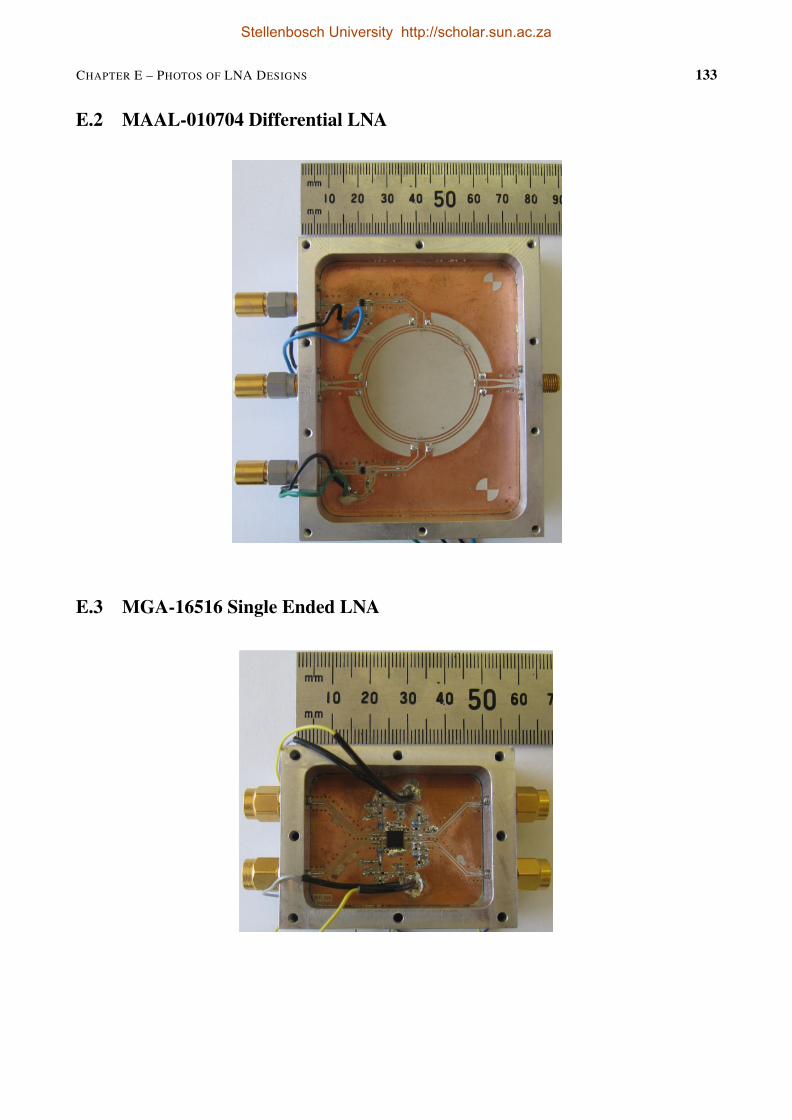
CHAPTER E – PHOTOS OF LNA DESIGNS 133
E.2 MAAL-010704 Differential LNA
E.3 MGA-16516 Single Ended LNA
Stellenbosch University http://scholar.sun.ac.za
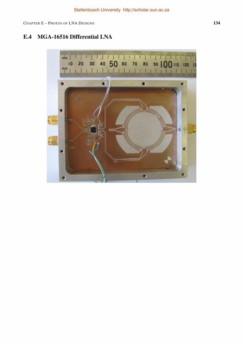
CHAPTER E – PHOTOS OF LNA DESIGNS 134
E.4 MGA-16516 Differential LNA
Stellenbosch University http://scholar.sun.ac.za

List of References
[1] SPDO. (2011, May) The square kilometer arry fact sheet for industry. [Online]. Available: http://www.
skatelescope.org/wp-content/uploads/2011/03/SKA_Factsheet-for-Industry_May2011_web.pdf ix, 2
[2] Agilent, “Fundamentals of rf and microwave noise figure measurement: Application note 57-1,” Agilent
Technologies, Tech. Rep., 2006. x, 55, 57
[3] L. Tiemeijer, R. Havens, R. de Kort, and A. Scholten, “Improved y-factor method for wide-band on-wafer
noise-parameter measurements,” Microwave Theory and Techniques, IEEE Transactions on, vol. 53, no. 9,
pp. 2917 – 2925, sept. 2005. x, 66, 67
[4] A. Abidi and J. Leete, “De-embedding the noise figure of differential amplifiers,” Solid-State Circuits,
IEEE Journal of, vol. 34, no. 6, pp. 882 –885, jun 1999. x, 68, 69
[5] L. Tiemeijer, R. Pijper, and E. van der Heijden, “Complete on-wafer noise-figure characterization of 60-
ghz differential amplifiers,” Microwave Theory and Techniques, IEEE Transactions on, vol. 58, no. 6, pp.
1599 –1608, 2010. x, 4, 71, 104
[6] (2011, January) Meerkat specifications and science. [Online]. Available: http://www.ska.ac.za/meerkat/
specsci.php 3
[7] (2011, January) Askap technologies. [Online]. Available: http://www.atnf.csiro.au/projects/askap/
technology.html 3, 4
[8] SKA. (2011) Precursors, pathfinders and design studies. [Online]. Available: http://www.skatelescope.
org/the-organisation/precursors-pathfinders-design-studies/ 3
[9] O. Garcia-Perez, L. Garcia-Munoz, J. Serna-Puente, V. Gonzalez-Posadas, J. Vazquez-Roy, and
D. Segovia-Vargas, “Differential active antennas for the ska project,” in Antennas and Propagation, 2009.
EuCAP 2009. 3rd European Conference on, march 2009, pp. 1316 –1319. 4
[10] J. de Vaate, L. Bakker, E. Woestenburg, R. Witvers, G. Kant, and W. van Cappellen, “Low cost low noise
phased-array feeding systems for ska pathfinders,” in Antenna Technology and Applied Electromagnetics
and the Canadian Radio Science Meeting, 2009. ANTEM/URSI 2009. 13th International Symposium on,
feb. 2009, pp. 1 –4. 4
[11] D. MacDonald, “The brownian movement and spontaneous fluctuations of electricity,” Res. Appl. in In-
dustry, vol. 1, pp. 194–203, 1948. 6, 8
135
Stellenbosch University http://scholar.sun.ac.za
LIST OF REFERENCES 136
[12] B. Oliver, “Thermal and quantum noise,” Proceedings of the IEEE, vol. 53, no. 5, pp. 436 – 454, may
1965. 6, 8
[13] J. B. Johnson, “Electronic noise: the first two decades,” Spectrum, IEEE, vol. 8, no. 2, pp. 42 –46, feb.
1971. 6, 8
[14] J. Ragazzini and S. Chang, “Noise and random processes,” Proceedings of the IRE, vol. 50, no. 5, pp.
1146 –1151, may 1962. 7
[15] D. Pozar, Microwave Engineering, 3rd ed. John Wiley & Sons, Inc., 2005. 8, 33, 45, 47, 57, 83, 86
[16] G. Vasilescu, Electronic Noise and Interfering Signals: Principles and Applications. Springer, 2005. 9,
10
[17] J. Motchenbacher, C.D. Connelly, Low-Noise Electronic System Design. John Wiley & Sons, Inc., 1993.
9, 10, 11, 20, 21
[18] W. Shockley, “The path to the conception of the junction transistor,” Electron Devices, IEEE Transactions
on, vol. 31, no. 11, pp. 1523 – 1546, nov 1984. 10
[19] A. van der Ziel, “Theory of shot noise in junction diodes and junction transistors,” Proceedings of the IRE,
vol. 43, no. 11, pp. 1639 –1646, nov. 1955. 10
[20] D. Peterson, “Noise performance of transistors,” Electron Devices, IRE Transactions on, vol. 9, no. 3, pp.
296 –303, may 1962. 10
[21] H. Fukui, “The noise performance of microwave transistors,” Electron Devices, IEEE Transactions on,
vol. 13, no. 3, pp. 329 – 341, mar 1966. 10, 21
[22] A. Van Der Ziel, “Thermal noise in field-effect transistors,” Proceedings of the IRE, vol. 50, no. 8, pp.
1808 –1812, aug. 1962. 14
[23] ——, “Gate noise in field effect transistors at moderately high frequencies,” Proceedings of the IEEE,
vol. 51, no. 3, pp. 461 – 467, march 1963. 14
[24] R. Pucel, D. Masse, and C. Krumm, “Noise performance of gallium arsenide field-effect transistors,”
Solid-State Circuits, IEEE Journal of, vol. 11, no. 2, pp. 243 – 255, apr 1976. 15, 24
[25] A. Cappy, “Noise modeling and measurement techniques [hemts],” Microwave Theory and Techniques,
IEEE Transactions on, vol. 36, no. 1, pp. 1 –10, jan 1988. 15
[26] H. Fukui, “Design of microwave gaas mesfet’s for broad-band low-noise amplifiers,” Microwave Theory
and Techniques, IEEE Transactions on, vol. 27, no. 7, pp. 643 – 650, jul 1979. 15
[27] M. Pospieszalski, “Modeling of noise parameters of mesfets and modfets and their frequency and tempe-
rature dependence,” Microwave Theory and Techniques, IEEE Transactions on, vol. 37, no. 9, pp. 1340
–1350, sep 1989. 15, 30
Stellenbosch University http://scholar.sun.ac.za
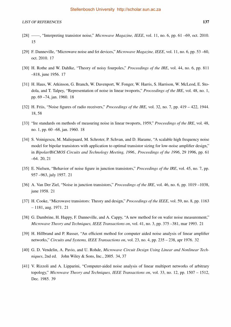
LIST OF REFERENCES 137
[28] ——, “Interpreting transistor noise,” Microwave Magazine, IEEE, vol. 11, no. 6, pp. 61 –69, oct. 2010.
15
[29] F. Danneville, “Microwave noise and fet devices,” Microwave Magazine, IEEE, vol. 11, no. 6, pp. 53 –60,
oct. 2010. 17
[30] H. Rothe and W. Dahlke, “Theory of noisy fourpoles,” Proceedings of the IRE, vol. 44, no. 6, pp. 811
–818, june 1956. 17
[31] H. Haus, W. Atkinson, G. Branch, W. Davenport, W. Fonger, W. Harris, S. Harrison, W. McLeod, E. Sto-
dola, and T. Talpey, “Representation of noise in linear twoports,” Proceedings of the IRE, vol. 48, no. 1,
pp. 69 –74, jan. 1960. 18
[32] H. Friis, “Noise figures of radio receivers,” Proceedings of the IRE, vol. 32, no. 7, pp. 419 – 422, 1944.
18, 58
[33] “Ire standards on methods of measuring noise in linear twoports, 1959,” Proceedings of the IRE, vol. 48,
no. 1, pp. 60 –68, jan. 1960. 18
[34] S. Voinigescu, M. Maliepaard, M. Schroter, P. Schvan, and D. Harame, “A scalable high frequency noise
model for bipolar transistors with application to optimal transistor sizing for low-noise amplifier design,”
in Bipolar/BiCMOS Circuits and Technology Meeting, 1996., Proceedings of the 1996, 29 1996, pp. 61
–64. 20, 21
[35] E. Nielsen, “Behavior of noise figure in junction transistors,” Proceedings of the IRE, vol. 45, no. 7, pp.
957 –963, july 1957. 21
[36] A. Van Der Ziel, “Noise in junction transistors,” Proceedings of the IRE, vol. 46, no. 6, pp. 1019 –1038,
june 1958. 21
[37] H. Cooke, “Microwave transistors: Theory and design,” Proceedings of the IEEE, vol. 59, no. 8, pp. 1163
– 1181, aug. 1971. 21
[38] G. Dambrine, H. Happy, F. Danneville, and A. Cappy, “A new method for on wafer noise measurement,”
Microwave Theory and Techniques, IEEE Transactions on, vol. 41, no. 3, pp. 375 –381, mar 1993. 21
[39] H. Hillbrand and P. Russer, “An efficient method for computer aided noise analysis of linear amplifier
networks,” Circuits and Systems, IEEE Transactions on, vol. 23, no. 4, pp. 235 – 238, apr 1976. 32
[40] G. D. Vendelin, A. Pavio, and U. Rohde, Microwave Circuit Design Using Linear and Nonlinear Tech-
niques, 2nd ed. John Wiley & Sons, Inc., 2005. 34, 37
[41] V. Rizzoli and A. Lipparini, “Computer-aided noise analysis of linear multiport networks of arbitrary
topology,” Microwave Theory and Techniques, IEEE Transactions on, vol. 33, no. 12, pp. 1507 – 1512,
Dec. 1985. 39
Stellenbosch University http://scholar.sun.ac.za
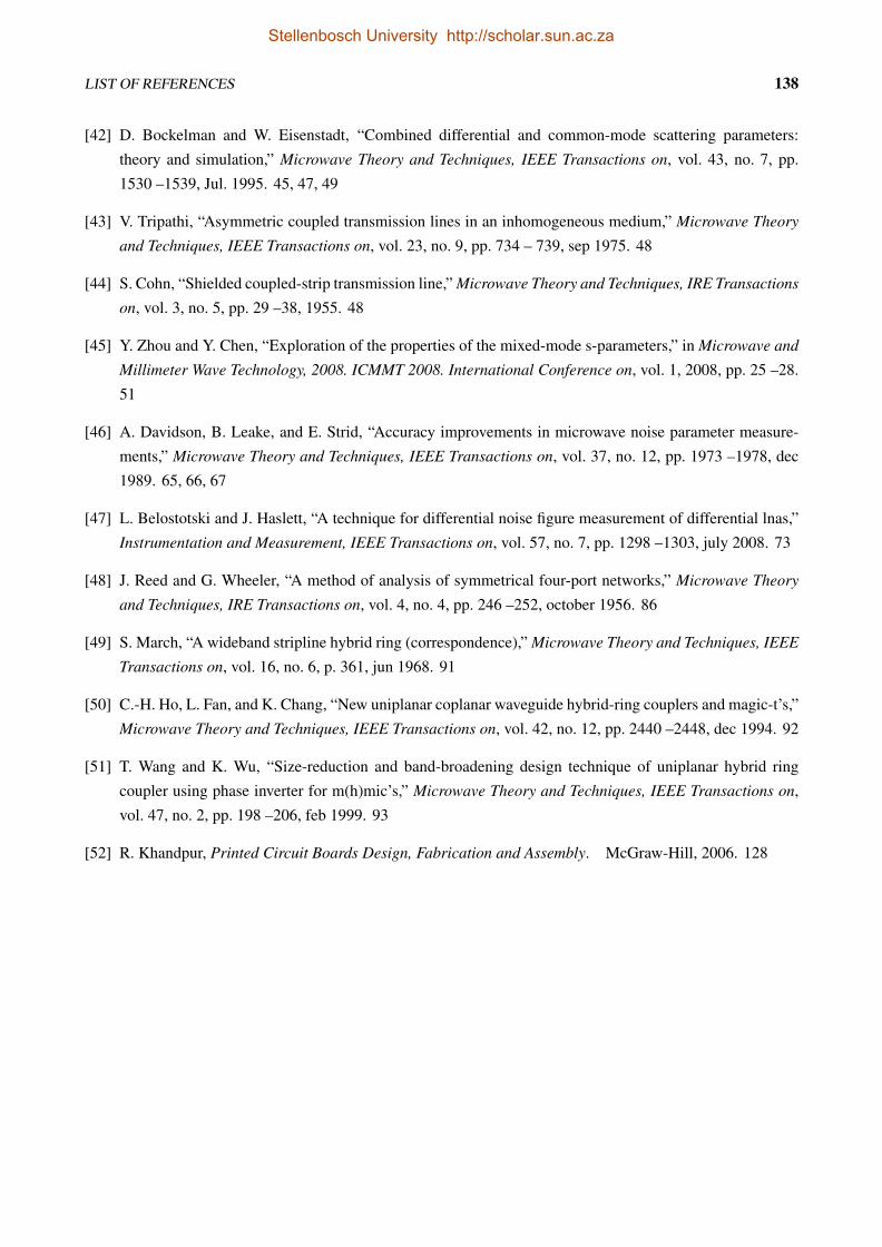
LIST OF REFERENCES 138
[42] D. Bockelman and W. Eisenstadt, “Combined differential and common-mode scattering parameters:
theory and simulation,” Microwave Theory and Techniques, IEEE Transactions on, vol. 43, no. 7, pp.
1530 –1539, Jul. 1995. 45, 47, 49
[43] V. Tripathi, “Asymmetric coupled transmission lines in an inhomogeneous medium,” Microwave Theory
and Techniques, IEEE Transactions on, vol. 23, no. 9, pp. 734 – 739, sep 1975. 48
[44] S. Cohn, “Shielded coupled-strip transmission line,” Microwave Theory and Techniques, IRE Transactions
on, vol. 3, no. 5, pp. 29 –38, 1955. 48
[45] Y. Zhou and Y. Chen, “Exploration of the properties of the mixed-mode s-parameters,” in Microwave and
Millimeter Wave Technology, 2008. ICMMT 2008. International Conference on, vol. 1, 2008, pp. 25 –28.
51
[46] A. Davidson, B. Leake, and E. Strid, “Accuracy improvements in microwave noise parameter measure-
ments,” Microwave Theory and Techniques, IEEE Transactions on, vol. 37, no. 12, pp. 1973 –1978, dec
1989. 65, 66, 67
[47] L. Belostotski and J. Haslett, “A technique for differential noise figure measurement of differential lnas,”
Instrumentation and Measurement, IEEE Transactions on, vol. 57, no. 7, pp. 1298 –1303, july 2008. 73
[48] J. Reed and G. Wheeler, “A method of analysis of symmetrical four-port networks,” Microwave Theory
and Techniques, IRE Transactions on, vol. 4, no. 4, pp. 246 –252, october 1956. 86
[49] S. March, “A wideband stripline hybrid ring (correspondence),” Microwave Theory and Techniques, IEEE
Transactions on, vol. 16, no. 6, p. 361, jun 1968. 91
[50] C.-H. Ho, L. Fan, and K. Chang, “New uniplanar coplanar waveguide hybrid-ring couplers and magic-t’s,”
Microwave Theory and Techniques, IEEE Transactions on, vol. 42, no. 12, pp. 2440 –2448, dec 1994. 92
[51] T. Wang and K. Wu, “Size-reduction and band-broadening design technique of uniplanar hybrid ring
coupler using phase inverter for m(h)mic’s,” Microwave Theory and Techniques, IEEE Transactions on,
vol. 47, no. 2, pp. 198 –206, feb 1999. 93
[52] R. Khandpur, Printed Circuit Boards Design, Fabrication and Assembly. McGraw-Hill, 2006. 128
Stellenbosch University http://scholar.sun.ac.za
Related Documents