Computer Organization and Architecture Chapter 1 : Introduction Compiled By: Er. Hari Aryal [[email protected]] Reference: W. Stallings | 1 Chapter – 1 Introduction 1.1 Computer Organization and Architecture Computer Architecture refers to those attributes of a system that have a direct impact on the logical execution of a program. Examples: o the instruction set o the number of bits used to represent various data types o I/O mechanisms o memory addressing techniques Computer Organization refers to the operational units and their interconnections that realize the architectural specifications. Examples are things that are transparent to the programmer: o control signals o interfaces between computer and peripherals o the memory technology being used So, for example, the fact that a multiply instruction is available is a computer architecture issue. How that multiply is implemented is a computer organization issue. • Architecture is those attributes visible to the programmer o Instruction set, number of bits used for data representation, I/O mechanisms, addressing techniques. o e.g. Is there a multiply instruction? • Organization is how features are implemented o Control signals, interfaces, memory technology. o e.g. Is there a hardware multiply unit or is it done by repeated addition? • All Intel x86 family share the same basic architecture • The IBM System/370 family share the same basic architecture • This gives code compatibility o At least backwards • Organization differs between different versions 1.2 Structure and Function • Structure is the way in which components relate to each other • Function is the operation of individual components as part of the structure • All computer functions are: o Data processing: Computer must be able to process data which may take a wide variety of forms and the range of processing. o Data storage: Computer stores data either temporarily or permanently. o Data movement: Computer must be able to move data between itself and the outside world. o Control: There must be a control of the above three functions.

Welcome message from author
This document is posted to help you gain knowledge. Please leave a comment to let me know what you think about it! Share it to your friends and learn new things together.
Transcript
Computer Organization and Architecture Chapter 1 : Introduction
Compiled By: Er. Hari Aryal [[email protected]] Reference: W. Stallings | 1
Chapter – 1
Introduction
1.1 Computer Organization and Architecture
Computer Architecture refers to those attributes of a system that have a direct impact on
the logical execution of a program. Examples:
o the instruction set
o the number of bits used to represent various data types
o I/O mechanisms
o memory addressing techniques
Computer Organization refers to the operational units and their interconnections that
realize the architectural specifications. Examples are things that are transparent to the
programmer:
o control signals
o interfaces between computer and peripherals
o the memory technology being used
So, for example, the fact that a multiply instruction is available is a computer architecture
issue. How that multiply is implemented is a computer organization issue.
• Architecture is those attributes visible to the programmer
o Instruction set, number of bits used for data representation, I/O mechanisms,
addressing techniques.
o e.g. Is there a multiply instruction?
• Organization is how features are implemented
o Control signals, interfaces, memory technology.
o e.g. Is there a hardware multiply unit or is it done by repeated addition?
• All Intel x86 family share the same basic architecture
• The IBM System/370 family share the same basic architecture
• This gives code compatibility
o At least backwards
• Organization differs between different versions
1.2 Structure and Function
• Structure is the way in which components relate to each other
• Function is the operation of individual components as part of the structure
• All computer functions are:
o Data processing: Computer must be able to process data which may take a wide
variety of forms and the range of processing.
o Data storage: Computer stores data either temporarily or permanently.
o Data movement: Computer must be able to move data between itself and the
outside world.
o Control: There must be a control of the above three functions.

Computer Organization and Architecture Chapter 1 : Introduction
Compiled By: Er. Hari Aryal [[email protected]] Reference: W. Stallings | 2
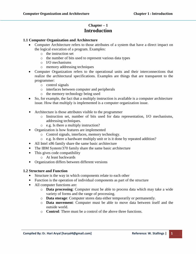
Fig: Functional view of a computer
Fig: Data movement operation Fig: Storage Operation
Computer Organization and Architecture Chapter 1 : Introduction
Compiled By: Er. Hari Aryal [[email protected]] Reference: W. Stallings | 3
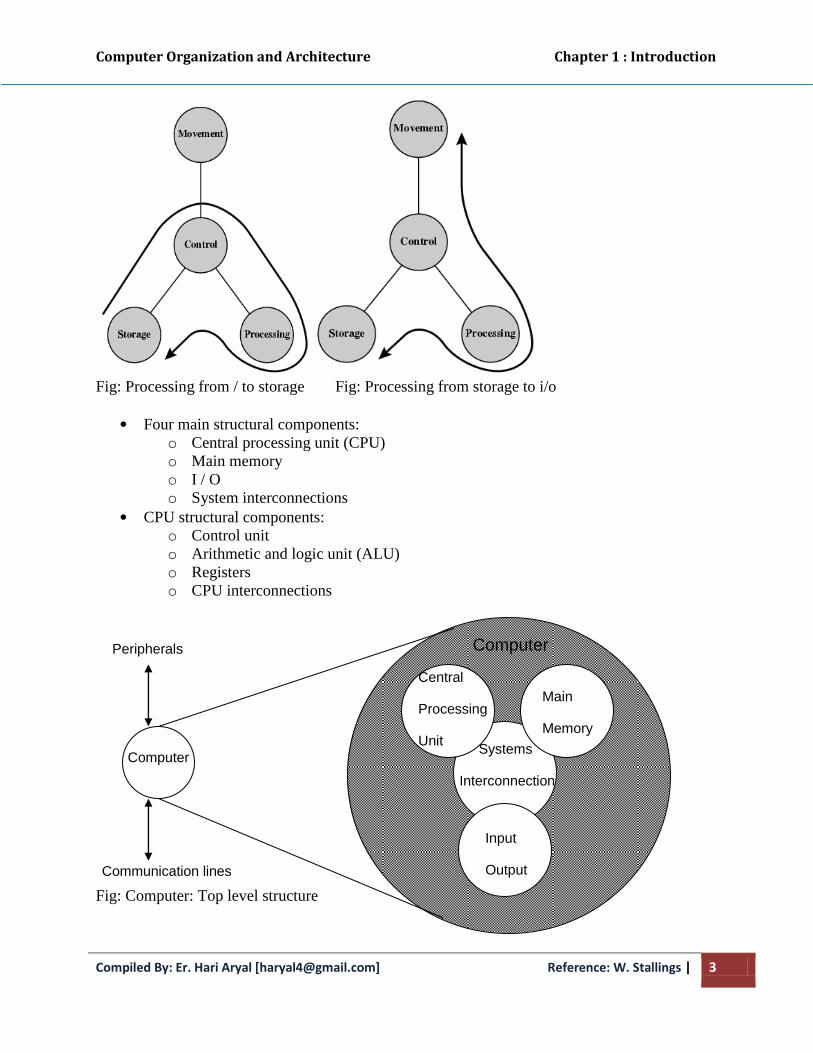
Fig: Processing from / to storage Fig: Processing from storage to i/o
• Four main structural components:
o Central processing unit (CPU)
o Main memory
o I / O
o System interconnections
• CPU structural components:
o Control unit
o Arithmetic and logic unit (ALU)
o Registers
o CPU interconnections
Fig: Computer: Top level structure
Computer
Main
Memory
Input
Output
Systems
Interconnection
Peripherals
Communication lines
Central
Processing
Unit
Computer

Computer Organization and Architecture Chapter 1 : Introduction
Compiled By: Er. Hari Aryal [[email protected]] Reference: W. Stallings | 4
Fig: The central processing unit
Fig: The control unit
1.3 Designing for performance
Some of the driving factors behind the need to design for performance:
• Microprocessor Speed
Pipelining
On board cache, on board L1 & L2 cache
Branch prediction: The processor looks ahead in the instruction code fetched from
memory and predicts which branches, or group of instructions are likely to be
processed next.
Data flow analysis: The processor analyzes which instructions are dependent on
each other’s results, or data, to create an optimized schedule of instructions to
prevent delay.
Computer Arithmetic
and
Login Unit
Control
Unit
Internal CPU
Interconnection
Registers
CPU
I/O
Memory
System
Bus
CPU
CPU
Control
Memory
Control Unit
Registers and
Decoders
Sequencing
Login Control
Unit
ALU
Registers
Internal
Bus
Interconn
ection
Bus
Control Unit
Computer Organization and Architecture Chapter 1 : Introduction
Compiled By: Er. Hari Aryal [[email protected]] Reference: W. Stallings | 5
Speculative execution: Using branch prediction and data flow analysis, some
processors speculatively execute instructions ahead of their actual appearance in
the program execution, holding the results in temporary locations.
• Performance Mismatch
Processor speed increased
Memory capacity increased
Memory speed lags behind processor speed
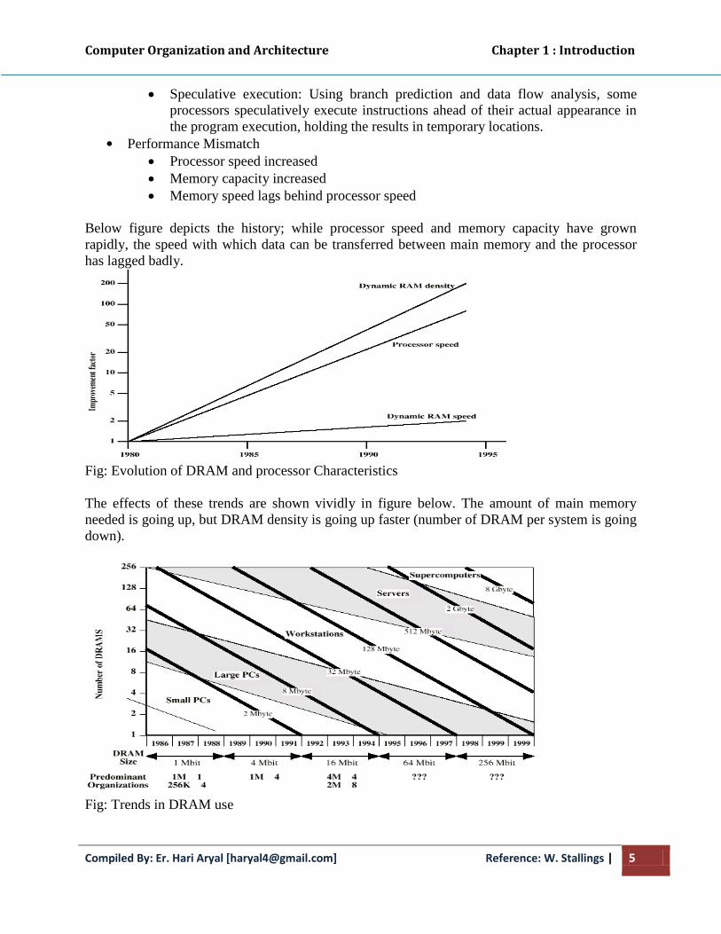
Below figure depicts the history; while processor speed and memory capacity have grown
rapidly, the speed with which data can be transferred between main memory and the processor
has lagged badly.
Fig: Evolution of DRAM and processor Characteristics
The effects of these trends are shown vividly in figure below. The amount of main memory
needed is going up, but DRAM density is going up faster (number of DRAM per system is going
down).
Fig: Trends in DRAM use

Computer Organization and Architecture Chapter 1 : Introduction
Compiled By: Er. Hari Aryal [[email protected]] Reference: W. Stallings | 6
Solutions
Increase number of bits retrieved at one time
o Make DRAM “wider” rather than “deeper” to use wide bus data paths.
Change DRAM interface
o Cache
Reduce frequency of memory access
o More complex cache and cache on chip
Increase interconnection bandwidth
o High speed buses
o Hierarchy of buses
1.4 Computer Components
• The Control Unit (CU) and the Arithmetic and Logic Unit (ALU) constitute the Central
Processing Unit (CPU)
• Data and instructions need to get into the system and results need to get out
o Input/output (I/O module)
• Temporary storage of code and results is needed
o Main memory (RAM)
• Program Concept
o Hardwired systems are inflexible
o General purpose hardware can do different tasks, given correct control signals
o Instead of re-wiring, supply a new set of control signals
Fig: Hardware and Software Approaches
Computer Organization and Architecture Chapter 1 : Introduction
Compiled By: Er. Hari Aryal [[email protected]] Reference: W. Stallings | 7
Fig: Computer Components; Top-Level View
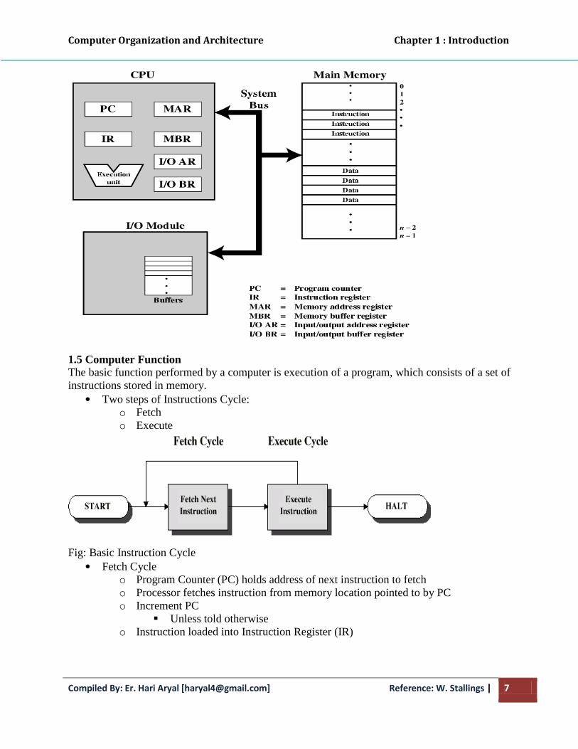
1.5 Computer Function
The basic function performed by a computer is execution of a program, which consists of a set of
instructions stored in memory.
• Two steps of Instructions Cycle:
o Fetch
o Execute
Fig: Basic Instruction Cycle
• Fetch Cycle
o Program Counter (PC) holds address of next instruction to fetch
o Processor fetches instruction from memory location pointed to by PC
o Increment PC
Unless told otherwise
o Instruction loaded into Instruction Register (IR)
Computer Organization and Architecture Chapter 1 : Introduction
Compiled By: Er. Hari Aryal [[email protected]] Reference: W. Stallings | 8
• Execute Cycle
o Processor interprets instruction and performs required actions, such as:
Processor - memory
o data transfer between CPU and main memory
Processor - I/O
o Data transfer between CPU and I/O module
Data processing
o Some arithmetic or logical operation on data
Control
o Alteration of sequence of operations
o e.g. jump
Combination of above
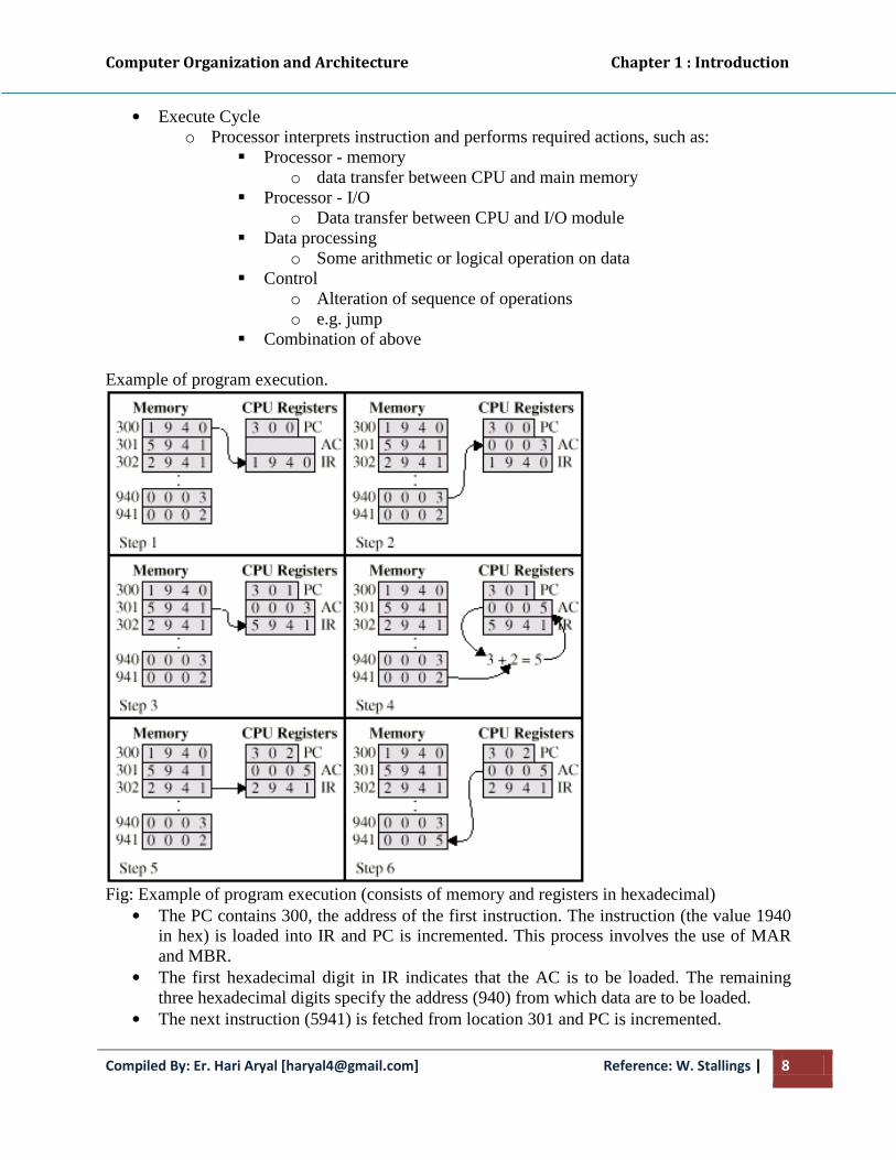
Example of program execution.
Fig: Example of program execution (consists of memory and registers in hexadecimal)
• The PC contains 300, the address of the first instruction. The instruction (the value 1940
in hex) is loaded into IR and PC is incremented. This process involves the use of MAR
and MBR.
• The first hexadecimal digit in IR indicates that the AC is to be loaded. The remaining
three hexadecimal digits specify the address (940) from which data are to be loaded.
• The next instruction (5941) is fetched from location 301 and PC is incremented.

Computer Organization and Architecture Chapter 1 : Introduction
Compiled By: Er. Hari Aryal [[email protected]] Reference: W. Stallings | 9
• The old contents of AC and the contents of location 941 are added and the result is stored
in the AC.
• The next instruction (2941) is fetched from location 302 and the PC is incremented.
• The contents of the AC are stored in location 941.
Fig: Instruction cycle state diagram
Interrupts:
• Mechanism by which other modules (e.g. I/O) may interrupt normal sequence of
processing
• Program
o e.g. overflow, division by zero
• Timer
o Generated by internal processor timer
o Used in pre-emptive multi-tasking
• I/O
o from I/O controller
• Hardware failure
o e.g. memory parity error

Computer Organization and Architecture Chapter 1 : Introduction
Compiled By: Er. Hari Aryal [[email protected]] Reference: W. Stallings | 10
Figure: Program flow of control without and with interrupts
• Instruction Cycle
o Added to instruction cycle
o Processor checks for interrupt
Indicated by an interrupt signal
o If no interrupt, fetch next instruction
o If interrupt pending:
Suspend execution of current program
Save context
Set PC to start address of interrupt handler routine
Process interrupt
Restore context and continue interrupted program
Fig: Transfer of control via interrupts

Computer Organization and Architecture Chapter 1 : Introduction
Compiled By: Er. Hari Aryal [[email protected]] Reference: W. Stallings | 11
Fig: Instruction Cycle with Interrupts
Fig: Instruction cycle state diagram, with interrupts
• Multiple Interrupts
o Disable interrupts (approach #1)
Processor will ignore further interrupts whilst processing one interrupt
Interrupts remain pending and are checked after first interrupt has been
processed
Interrupts handled in sequence as they occur
o Define priorities (approach #2)
Low priority interrupts can be interrupted by higher priority interrupts
When higher priority interrupt has been processed, processor returns to
previous interrupt
1.6 Interconnection structures
The collection of paths connecting the various modules is called the interconnecting structure.
• All the units must be connected
• Different type of connection for different type of unit
o Memory
o Input/Output
o CPU
Computer Organization and Architecture Chapter 1 : Introduction
Compiled By: Er. Hari Aryal [[email protected]] Reference: W. Stallings | 12
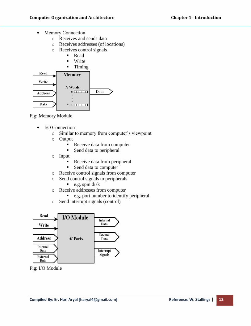
• Memory Connection
o Receives and sends data
o Receives addresses (of locations)
o Receives control signals
Read
Write
Timing
Fig: Memory Module
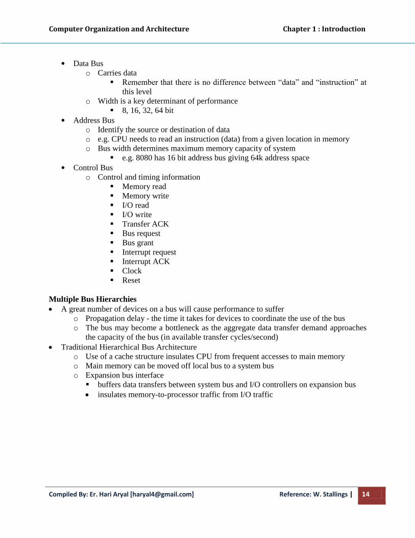
• I/O Connection
o Similar to memory from computer’s viewpoint
o Output
Receive data from computer
Send data to peripheral
o Input
Receive data from peripheral
Send data to computer
o Receive control signals from computer
o Send control signals to peripherals
e.g. spin disk
o Receive addresses from computer
e.g. port number to identify peripheral
o Send interrupt signals (control)
Fig: I/O Module

Computer Organization and Architecture Chapter 1 : Introduction
Compiled By: Er. Hari Aryal [[email protected]] Reference: W. Stallings | 13
• CPU Connection
o Reads instruction and data
o Writes out data (after processing)
o Sends control signals to other units
o Receives (& acts on) interrupts
Fig: CPU Module
1.7 Bus interconnection
• A bus is a communication pathway connecting two or more devices
• Usually broadcast (all components see signal)
• Often grouped
o A number of channels in one bus
o e.g. 32 bit data bus is 32 separate single bit channels
• Power lines may not be shown
• There are a number of possible interconnection systems
• Single and multiple BUS structures are most common
• e.g. Control/Address/Data bus (PC)
• e.g. Unibus (DEC-PDP)
• Lots of devices on one bus leads to:
o Propagation delays
o Long data paths mean that co-ordination of bus use can adversely affect
performance
o If aggregate data transfer approaches bus capacity
• Most systems use multiple buses to overcome these problems
Fig: Bus Interconnection Scheme
Computer Organization and Architecture Chapter 1 : Introduction
Compiled By: Er. Hari Aryal [[email protected]] Reference: W. Stallings | 14
• Data Bus
o Carries data
Remember that there is no difference between “data” and “instruction” at
this level
o Width is a key determinant of performance
8, 16, 32, 64 bit
• Address Bus
o Identify the source or destination of data
o e.g. CPU needs to read an instruction (data) from a given location in memory
o Bus width determines maximum memory capacity of system
e.g. 8080 has 16 bit address bus giving 64k address space
• Control Bus
o Control and timing information
Memory read
Memory write
I/O read
I/O write
Transfer ACK
Bus request
Bus grant
Interrupt request
Interrupt ACK
Clock
Reset
Multiple Bus Hierarchies
A great number of devices on a bus will cause performance to suffer
o Propagation delay - the time it takes for devices to coordinate the use of the bus
o The bus may become a bottleneck as the aggregate data transfer demand approaches
the capacity of the bus (in available transfer cycles/second)
Traditional Hierarchical Bus Architecture
o Use of a cache structure insulates CPU from frequent accesses to main memory
o Main memory can be moved off local bus to a system bus
o Expansion bus interface
buffers data transfers between system bus and I/O controllers on expansion bus
insulates memory-to-processor traffic from I/O traffic

Computer Organization and Architecture Chapter 1 : Introduction
Compiled By: Er. Hari Aryal [[email protected]] Reference: W. Stallings | 15
Traditional Hierarchical Bus Architecture Example
High-performance Hierarchical Bus Architecture
o Traditional hierarchical bus breaks down as higher and higher performance is
seen in the I/O devices
o Incorporates a high-speed bus
specifically designed to support high-capacity I/O devices
brings high-demand devices into closer integration with the processor and at
the same time is independent of the processor
Changes in processor architecture do not affect the high-speed bus, and vice
versa
o Sometimes known as a mezzanine architecture

Computer Organization and Architecture Chapter 1 : Introduction
Compiled By: Er. Hari Aryal [[email protected]] Reference: W. Stallings | 16
High-performance Hierarchical Bus Architecture Example
Elements of Bus Design
• Bus Types
o Dedicated
Separate data & address lines
o Multiplexed
Shared lines
Address valid or data valid control line
Advantage - fewer lines
Disadvantages
o More complex control
o Ultimate performance
• Bus Arbitration
o More than one module controlling the bus
e.g. CPU and DMA controller
o Only one module may control bus at one time
o Arbitration may be centralised or distributed
• Centralised Arbitration
o Single hardware device controlling bus access
Bus Controller
Arbiter
o May be part of CPU or separate
• Distributed Arbitration

Computer Organization and Architecture Chapter 1 : Introduction
Compiled By: Er. Hari Aryal [[email protected]] Reference: W. Stallings | 17
o Each module may claim the bus
o Control logic on all modules
• Timing
o Co-ordination of events on bus
o Synchronous
Events determined by clock signals
Control Bus includes clock line
A single 1-0 is a bus cycle
All devices can read clock line
Usually sync on leading edge
Usually a single cycle for an event
• Bus Width
o Address: Width of address bus has an impact on system capacity i.e. wider bus
means greater the range of locations that can be transferred.
o Data: width of data bus has an impact on system performance i.e. wider bus
means number of bits transferred at one time.
• Data Transfer Type
o Read
o Write
o Read-modify-write
o Read-after-write
o Block
1.8 PCI
PCI is a popular high bandwidth, processor independent bus that can function as mezzanine
or peripheral bus.
PCI delivers better system performance for high speed I/O subsystems (graphic display
adapters, network interface controllers, disk controllers etc.)
PCI is designed to support a variety of microprocessor based configurations including both
single and multiple processor system.
It makes use of synchronous timing and centralised arbitration scheme.
PCI may be configured as a 32 or 64-bit bus.
Current Standard
o up to 64 data lines at 33Mhz
o requires few chips to implement
o supports other buses attached to PCI bus
o public domain, initially developed by Intel to support Pentium-based systems
o supports a variety of microprocessor-based configurations, including multiple
processors
o uses synchronous timing and centralized arbitration

Computer Organization and Architecture Chapter 1 : Introduction
Compiled By: Er. Hari Aryal [[email protected]] Reference: W. Stallings | 18
Typical Desktop System
Note: Bridge acts as a data buffer so that the speed of the PCI bus may differ from that of the
processor’s I/O capability.
Typical Server System
Note: In a multiprocessor system, one or more PCI configurations may be connected by bridges
to the processor’s system bus.
PCI Bus Lines
• Systems lines
o Including clock and reset
• Address & Data
o 32 time mux lines for address/data
o Interrupt & validate lines
• Interface Control
• Arbitration
o Not shared
o Direct connection to PCI bus arbiter

Computer Organization and Architecture Chapter 1 : Introduction
Compiled By: Er. Hari Aryal [[email protected]] Reference: W. Stallings | 19
• Error lines
• Interrupt lines
o Not shared
• Cache support
• 64-bit Bus Extension
o Additional 32 lines
o Time multiplexed
o 2 lines to enable devices to agree to use 64-bit transfer
• JTAG/Boundary Scan
o For testing procedures
PCI Commands
• Transaction between initiator (master) and target
• Master claims bus
• Determine type of transaction
o e.g. I/O read/write
• Address phase
• One or more data phases
PCI Enhancements: AGP
AGP – Advanced Graphics Port
o Called a port, not a bus because it only connects 2 devices

Computer Organization and Architecture Chapter 2 : Central Processing Unit
Compiled By: Er. Hari Aryal [[email protected]] References: W. Stalling & M. Mano | 1
Chapter – 2
Central Processing Unit
The part of the computer that performs the bulk of data processing operations is called the
Central Processing Unit (CPU) and is the central component of a digital computer. Its purpose is
to interpret instruction cycles received from memory and perform arithmetic, logic and control
operations with data stored in internal register, memory words and I/O interface units. A CPU is
usually divided into two parts namely processor unit (Register Unit and Arithmetic Logic Unit)
and control unit.
Fig: Components of CPU
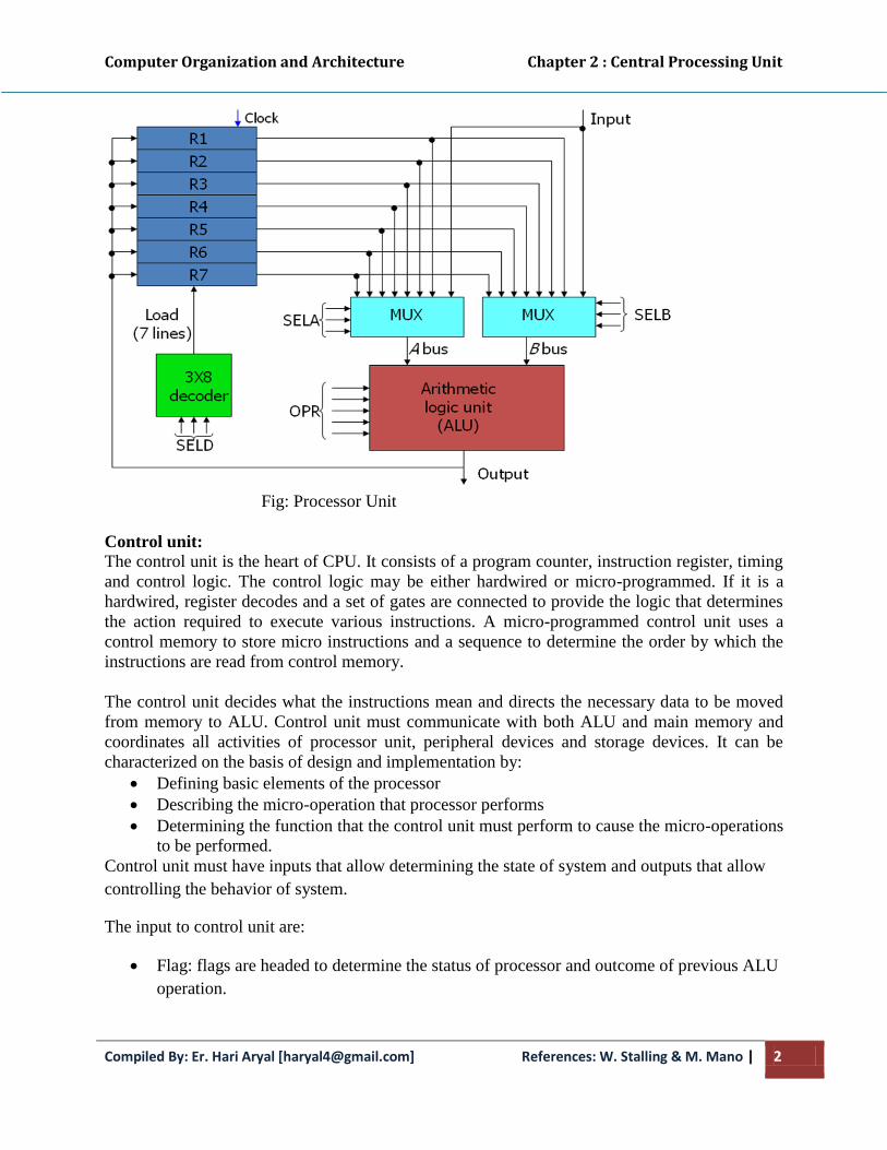
Processor Unit:
The processor unit consists of arithmetic unit, logic unit, a number of registers and internal buses
that provides data path for transfer of information between register and arithmetic logic unit. The
block diagram of processor unit is shown in figure below where all registers are connected
through common buses. The registers communicate each other not only for direct data transfer
but also while performing various micro-operations.
Here two sets of multiplexers select register which perform input data for ALU. A decoder
selects destination register by enabling its load input. The function select in ALU determines the
particular operation that to be performed.
For an example to perform the operation: R3 R1 + R2
1. MUX A selector (SELA): to place the content of R1 into bus A.
2. MUX B selector (SELB): to place the content of R2 into bus B.
3. ALU operation selector (OPR): to provide arithmetic addition A + B.
4. Decoder destination selector (SELD): to transfer the content of the output bus into R3.
Computer Organization and Architecture Chapter 2 : Central Processing Unit
Compiled By: Er. Hari Aryal [[email protected]] References: W. Stalling & M. Mano | 2
Fig: Processor Unit
Control unit:
The control unit is the heart of CPU. It consists of a program counter, instruction register, timing
and control logic. The control logic may be either hardwired or micro-programmed. If it is a
hardwired, register decodes and a set of gates are connected to provide the logic that determines
the action required to execute various instructions. A micro-programmed control unit uses a
control memory to store micro instructions and a sequence to determine the order by which the
instructions are read from control memory.
The control unit decides what the instructions mean and directs the necessary data to be moved
from memory to ALU. Control unit must communicate with both ALU and main memory and
coordinates all activities of processor unit, peripheral devices and storage devices. It can be
characterized on the basis of design and implementation by:
Defining basic elements of the processor
Describing the micro-operation that processor performs
Determining the function that the control unit must perform to cause the micro-operations
to be performed.
Control unit must have inputs that allow determining the state of system and outputs that allow
controlling the behavior of system.
The input to control unit are:
Flag: flags are headed to determine the status of processor and outcome of previous ALU
operation.

Computer Organization and Architecture Chapter 2 : Central Processing Unit
Compiled By: Er. Hari Aryal [[email protected]] References: W. Stalling & M. Mano | 3
Clock: All micro-operations are performed within each clock pulse. This clock pulse is
also called as processor cycle time or clock cycle time.
Instruction Register: The op-code of instruction determines which micro-operation to
perform during execution cycle.
Control signal from control bus: The control bus portion of system bus provides interrupt,
acknowledgement signals to control unit.
The outputs from control unit are:
Control signal within processor: These signals causes data transfer between registers,
activate ALU functions.
Control signal to control bus: These are signals to memory and I/O module. All these
control signals are applied directly as binary inputs to individual logic gate.
Fig: Control Unit
2.1 CPU Structure and Function
Processor Organization
Things a CPU must do:
- Fetch Instructions
- Interpret Instructions
- Fetch Data
- Process Data
- Write Data
Computer Organization and Architecture Chapter 2 : Central Processing Unit
Compiled By: Er. Hari Aryal [[email protected]] References: W. Stalling & M. Mano | 4
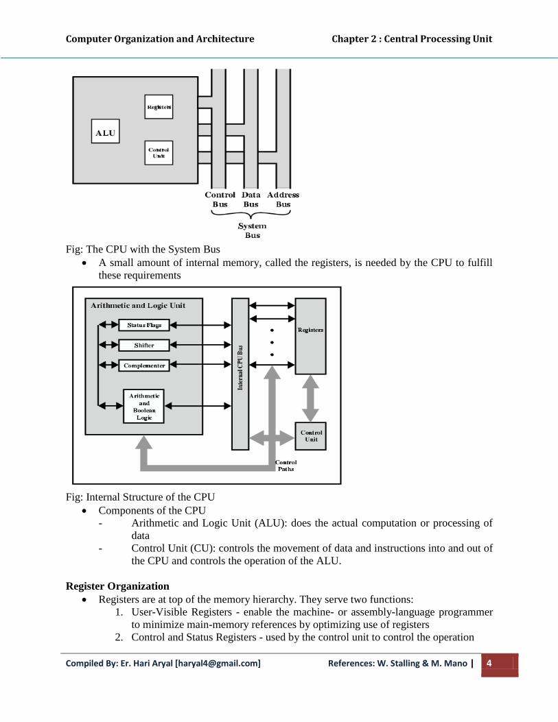
Fig: The CPU with the System Bus
A small amount of internal memory, called the registers, is needed by the CPU to fulfill
these requirements
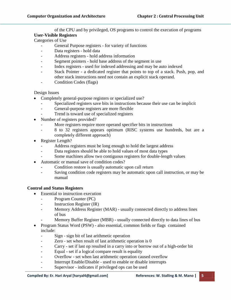
Fig: Internal Structure of the CPU
Components of the CPU
- Arithmetic and Logic Unit (ALU): does the actual computation or processing of
data
- Control Unit (CU): controls the movement of data and instructions into and out of
the CPU and controls the operation of the ALU.
Register Organization
Registers are at top of the memory hierarchy. They serve two functions:
1. User-Visible Registers - enable the machine- or assembly-language programmer
to minimize main-memory references by optimizing use of registers
2. Control and Status Registers - used by the control unit to control the operation
Computer Organization and Architecture Chapter 2 : Central Processing Unit
Compiled By: Er. Hari Aryal [[email protected]] References: W. Stalling & M. Mano | 5
of the CPU and by privileged, OS programs to control the execution of programs
User-Visible Registers
Categories of Use
- General Purpose registers - for variety of functions
- Data registers - hold data
- Address registers - hold address information
- Segment pointers - hold base address of the segment in use
- Index registers - used for indexed addressing and may be auto indexed
- Stack Pointer - a dedicated register that points to top of a stack. Push, pop, and
other stack instructions need not contain an explicit stack operand.
- Condition Codes (flags)
Design Issues
Completely general-purpose registers or specialized use?
- Specialized registers save bits in instructions because their use can be implicit
- General-purpose registers are more flexible
- Trend is toward use of specialized registers
Number of registers provided?
- More registers require more operand specifier bits in instructions
- 8 to 32 registers appears optimum (RISC systems use hundreds, but are a
completely different approach)
Register Length?
- Address registers must be long enough to hold the largest address
- Data registers should be able to hold values of most data types
- Some machines allow two contiguous registers for double-length values
Automatic or manual save of condition codes?
- Condition restore is usually automatic upon call return
- Saving condition code registers may be automatic upon call instruction, or may be
manual
Control and Status Registers
Essential to instruction execution
- Program Counter (PC)
- Instruction Register (IR)
- Memory Address Register (MAR) - usually connected directly to address lines
of bus
- Memory Buffer Register (MBR) - usually connected directly to data lines of bus
Program Status Word (PSW) - also essential, common fields or flags contained
include:
- Sign - sign bit of last arithmetic operation
- Zero - set when result of last arithmetic operation is 0
- Carry - set if last op resulted in a carry into or borrow out of a high-order bit
- Equal - set if a logical compare result is equality
- Overflow - set when last arithmetic operation caused overflow
- Interrupt Enable/Disable - used to enable or disable interrupts
- Supervisor - indicates if privileged ops can be used
Computer Organization and Architecture Chapter 2 : Central Processing Unit
Compiled By: Er. Hari Aryal [[email protected]] References: W. Stalling & M. Mano | 6
Other optional registers
- Pointer to a block of memory containing additional status info (like process
control blocks)
- An interrupt vector
- A system stack pointer
- A page table pointer
- I/O registers
Design issues
- Operating system support in CPU
- How to divide allocation of control information between CPU registers and first
part of main memory (usual tradeoffs apply)
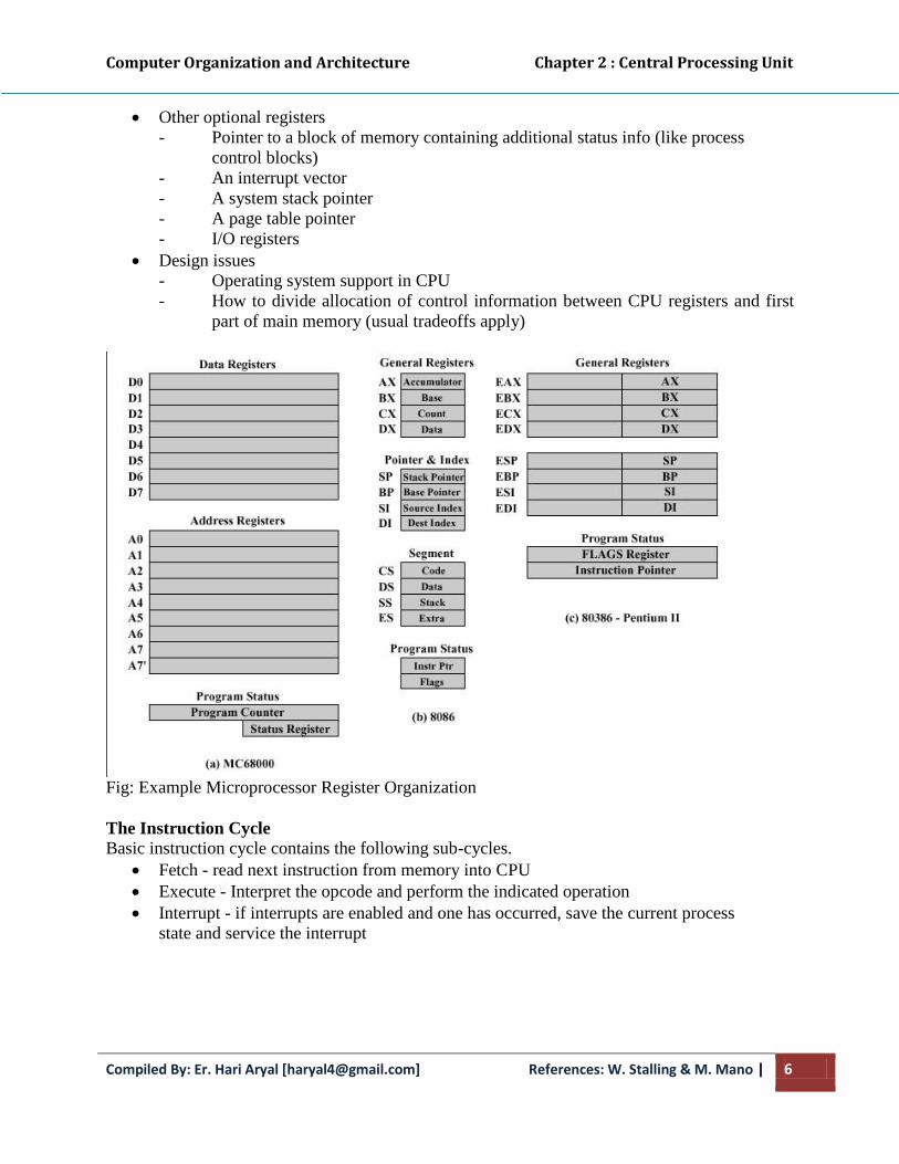
Fig: Example Microprocessor Register Organization
The Instruction Cycle
Basic instruction cycle contains the following sub-cycles.
Fetch - read next instruction from memory into CPU
Execute - Interpret the opcode and perform the indicated operation
Interrupt - if interrupts are enabled and one has occurred, save the current process
state and service the interrupt

Computer Organization and Architecture Chapter 2 : Central Processing Unit
Compiled By: Er. Hari Aryal [[email protected]] References: W. Stalling & M. Mano | 7
Fig: Instruction Cycles
Fig: Instruction Cycle State Diagram
The Indirect Cycle
- Think of as another instruction sub-cycle
- May require just another fetch (based upon last fetch)
- Might also require arithmetic, like indexing
Fig: Instruction Cycle with Indirect

Computer Organization and Architecture Chapter 2 : Central Processing Unit
Compiled By: Er. Hari Aryal [[email protected]] References: W. Stalling & M. Mano | 8
Data Flow
- Exact sequence depends on CPU design
- We can indicate sequence in general terms, assuming CPU employs:
a memory address register (MAR)
a memory buffer register (MBR)
a program counter (PC)
an instruction register (IR)
Fetch cycle data flow
- PC contains address of next instruction to be fetched
- This address is moved to MAR and placed on address bus
- Control unit requests a memory read
- Result is
placed on data bus
result copied to MBR
then moved to IR
- Meanwhile, PC is incremented
Fig: Data flow, Fetch Cycle
t1: MAR (PC)
t2: MBR Memory
PC PC + 1
t3: IR(Address) (MBR(Address))
Indirect cycle data flow - Decodes the instruction
- After fetch, control unit examines IR to see if indirect addressing is being used. If so:
- Rightmost n bits of MBR (the memory reference) are transferred to MAR
- Control unit requests a memory read, to get the desired operand address into the
MBR

Computer Organization and Architecture Chapter 2 : Central Processing Unit
Compiled By: Er. Hari Aryal [[email protected]] References: W. Stalling & M. Mano | 9
t1: MAR (IR(Address))
t2: MBR Memory
t3: IR(Address) (MBR(Address))
Fig: Data Flow, Indirect Cycle
Execute cycle data flow
- Not simple and predictable, like other cycles
- Takes many forms, since form depends on which of the various machine instructions
is in the IR
- May involve
transferring data among registers
read or write from memory or I/O
invocation of the ALU
For example: ADD R1, X
t1: MAR (IR(Address))
t2: MBR Memory
t3: R1 (R1) + (MBR)
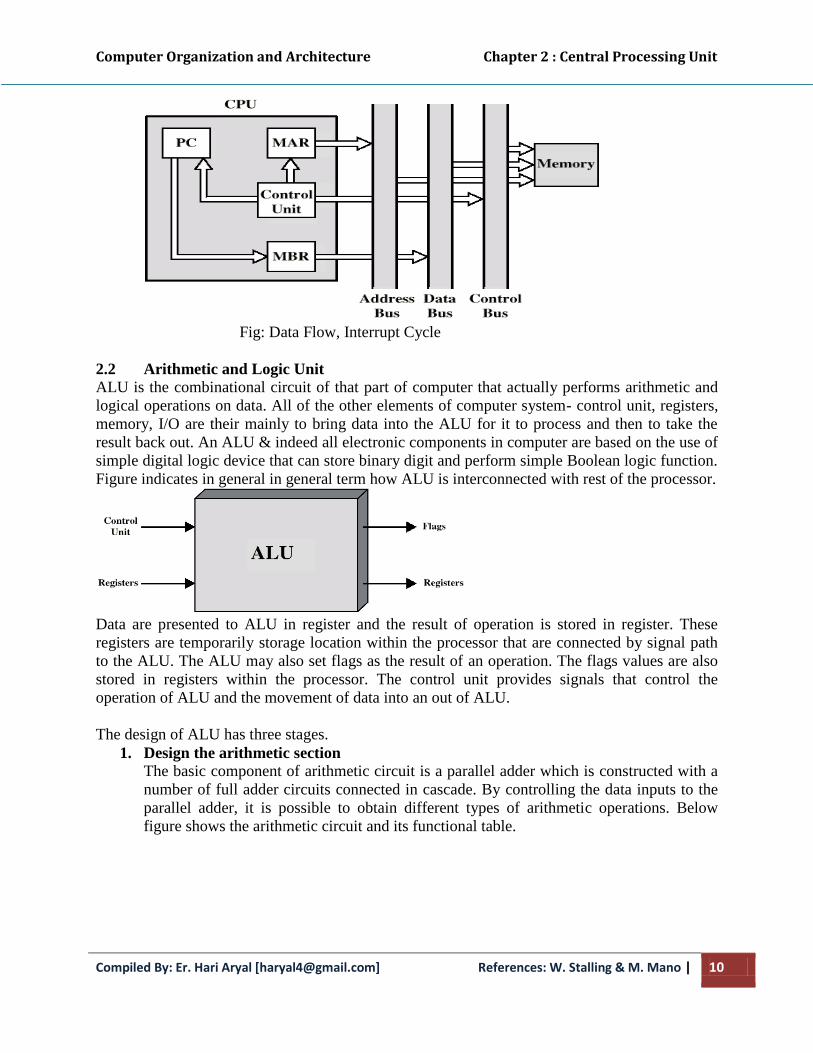
Interrupt cycle data flow
- Current contents of PC must be saved (for resume after interrupt), so PC is
transferred to MBR to be written to memory
- Save location’s address (such as a stack ptr) is loaded into MAR from the control unit
- PC is loaded with address of interrupt routine (so next instruction cycle will begin by
fetching appropriate instruction)
t1: MBR (PC)
t2: MAR save_address
PC Routine_address
t3: Memory (MBR)
Computer Organization and Architecture Chapter 2 : Central Processing Unit
Compiled By: Er. Hari Aryal [[email protected]] References: W. Stalling & M. Mano | 10
Fig: Data Flow, Interrupt Cycle
2.2 Arithmetic and Logic Unit
ALU is the combinational circuit of that part of computer that actually performs arithmetic and
logical operations on data. All of the other elements of computer system- control unit, registers,
memory, I/O are their mainly to bring data into the ALU for it to process and then to take the
result back out. An ALU & indeed all electronic components in computer are based on the use of
simple digital logic device that can store binary digit and perform simple Boolean logic function.
Figure indicates in general in general term how ALU is interconnected with rest of the processor.
Data are presented to ALU in register and the result of operation is stored in register. These
registers are temporarily storage location within the processor that are connected by signal path
to the ALU. The ALU may also set flags as the result of an operation. The flags values are also
stored in registers within the processor. The control unit provides signals that control the
operation of ALU and the movement of data into an out of ALU.
The design of ALU has three stages.
1. Design the arithmetic section
The basic component of arithmetic circuit is a parallel adder which is constructed with a
number of full adder circuits connected in cascade. By controlling the data inputs to the
parallel adder, it is possible to obtain different types of arithmetic operations. Below
figure shows the arithmetic circuit and its functional table.
Computer Organization and Architecture Chapter 2 : Central Processing Unit
Compiled By: Er. Hari Aryal [[email protected]] References: W. Stalling & M. Mano | 11
Fig: Block diagram of Arithmetic Unit
Functional table for arithmetic unit:
Select Input
Y
Output Microoperation
S1 S0 Cin = 0 Cin = 1 Cin = 0 Cin = 1
0 0 0 A A+1 Transfer A Increment A
0 1 B A+B A+B+1 Addition Addition with
carry
1 0 B’ A+B’ A+B’+1 Subtraction with
borrow
Subtraction
1 1 -1 A-1 A Decrement A Transfer A
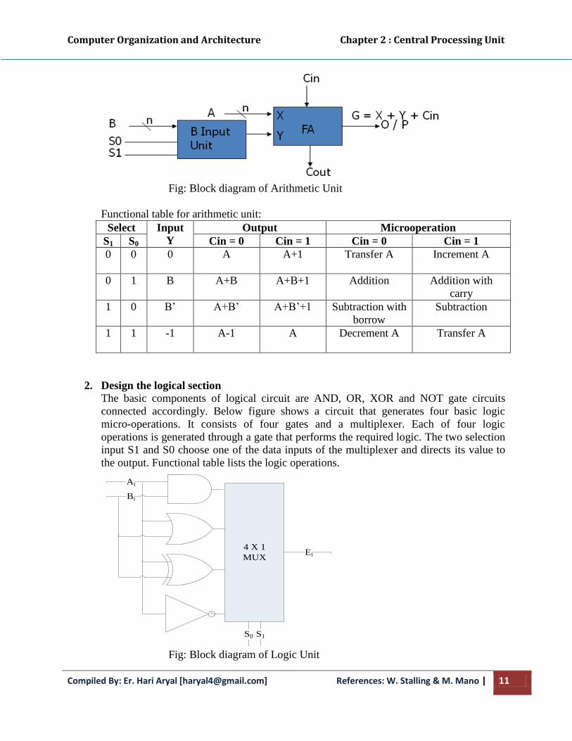
2. Design the logical section
The basic components of logical circuit are AND, OR, XOR and NOT gate circuits
connected accordingly. Below figure shows a circuit that generates four basic logic
micro-operations. It consists of four gates and a multiplexer. Each of four logic
operations is generated through a gate that performs the required logic. The two selection
input S1 and S0 choose one of the data inputs of the multiplexer and directs its value to
the output. Functional table lists the logic operations.
4 X 1
MUXEi
S1S0
Ai
Bi
Fig: Block diagram of Logic Unit

Computer Organization and Architecture Chapter 2 : Central Processing Unit
Compiled By: Er. Hari Aryal [[email protected]] References: W. Stalling & M. Mano | 12
Functional table for logic unit:
S1 S0 output Microoperation
0 0 Ai && Bi AND
0 1 Ai || Bi OR
1 0 Ai XOR Bi XOR
1 1 Ai’ NOT
3. Combine these 2 sections to form the ALU
Below figure shows a combined circuit of ALU where n data input from A are combined
with n data input from B to generate the result of an operation at the G output line. ALU
has a number of selection lines used to determine the operation to be performed. The
selection lines are decoded with the ALU so that selection lines can specify distinct
operations. The mode select S2 differentiate between arithmetic and logical operations.
The two functions select S1 and S0 specify the particular arithmetic and logic operations
to be performed. With three selection lines, it is possible to specify arithmetic operation
with S2 at 0 and logical operation with S2 at 1.
Fig: Block diagram of ALU

Computer Organization and Architecture Chapter 2 : Central Processing Unit
Compiled By: Er. Hari Aryal [[email protected]] References: W. Stalling & M. Mano | 13
Example: Design a 2-bit ALU that can perform addition, AND, OR, & XOR.
4 X 1
MUXResult0
4 X 1
MUXResult1
FA
A0
B0
A1
B1
Cin
S0S1
Cout
2.3 Instruction Formats
The computer can be used to perform a specific task, only by specifying the necessary steps to
complete the task. The collection of such ordered steps forms a ‘program’ of a computer. These
ordered steps are the instructions. Computer instructions are stored in central memory locations
and are executed sequentially one at a time. The control reads an instruction from a specific
address in memory and executes it. It then continues by reading the next instruction in sequence
and executes it until the completion of the program.
A computer usually has a variety of Instruction Code Formats. It is the function of the control
unit within the CPU to interpret each instruction code and provide the necessary control
functions needed to process the instruction. An n bit instruction that k bits in the address field
and m bits in the operation code field come addressed 2k location directly and specify 2
m
different operation.

Computer Organization and Architecture Chapter 2 : Central Processing Unit
Compiled By: Er. Hari Aryal [[email protected]] References: W. Stalling & M. Mano | 14
The bits of the instruction are divided into groups called fields.
The most common fields in instruction formats are:
o An Operation code field that specifies the operation to be performed.
o An Address field that designates a memory address or a processor
register.
o A Mode field that specifies the way the operand or the effective address is
determined.
n-1 m-1 k-1 0
Fig: Instruction format with mode field
The operation code field (Opcode) of an instruction is a group of bits that define various
processor operations such as add, subtract, complement, shift etcetera. The bits that define the
mode field of an instruction code specify a variety of alternatives for choosing the operands from
the given address. Operation specified by an instruction is executed on some data stored in the
processor register or in the memory location. Operands residing in memory are specified by their
memory address. Operands residing in processor register are specified with a register address.
Types of Instruction
Computers may have instructions of several different lengths containing varying
number of addresses.
The number of address fields in the instruction format of a computer depends on
the internal organization of its registers.
Most computers fall into one of 3 types of CPU organizations:
Single accumulator organization:- All the operations are performed with an
accumulator register. The instruction format in this type of computer uses one address
field. For example: ADD X, where X is the address of the operands .
General register organization:- The instruction format in this type of computer needs
three register address fields. For example: ADD R1,R2,R3
Stack organization:- The instruction in a stack computer consists of an operation code
with no address field. This operation has the effect of popping the 2 top numbers from the
stack, operating the numbers and pushing the sum into the stack. For example: ADD
Computers may have instructions of several different lengths containing varying number of
addresses. Following are the types of instructions.
1. Three address Instruction
With this type of instruction, each instruction specifies two operand location and a result
location. A temporary location T is used to store some intermediate result so as not to
alter any of the operand location. The three address instruction format requires a very
complex design to hold the three address references.
Format: Op X, Y, Z; X Y Op Z
Computer Organization and Architecture Chapter 2 : Central Processing Unit
Compiled By: Er. Hari Aryal [[email protected]] References: W. Stalling & M. Mano | 15
Example: ADD X, Y, Z; X Y + Z
ADVANTAGE: It results in short programs when evaluating arithmetic
expressions.
DISADVANTAGE: The instructions requires too many bits to specify 3
addresses.
2. Two address instruction
Two-address instructions are the most common in commercial computers. Here again
each address field can specify either a processor register, or a memory word. One address
must do double duty as both operand and result. The two address instruction format
reduces the space requirement. To avoid altering the value of an operand, a MOV
instruction is used to move one of the values to a result or temporary location T, before
performing the operation.
Format: Op X, Y; X X Op Y
Example: SUB X, Y; X X - Y
3. One address Instruction
It was generally used in earlier machine with the implied address been a CPU register
known as accumulator. The accumulator contains one of the operand and is used to store
the result. One-address instruction uses an implied accumulator (Ac) register for all data
manipulation. All operations are done between the AC register and a memory operand.
We use LOAD and STORE instruction for transfer to and from memory and Ac register.
Format: Op X; Ac Ac Op X
Example: MUL X; Ac Ac * X
4. Zero address Instruction
It does not use address field for the instruction like ADD, SUB, MUL, DIV etc. The
PUSH and POP instructions, however, need an address field to specify the operand that
communicates with the stack. The name “Zero” address is given because of the absence
of an address field in the computational instruction.
Format: Op; TOS TOS Op (TOS – 1)
Example: DIV; TOS TOS DIV (TOS – 1)
Example: To illustrate the influence of the number of address on computer programs, we will
evaluate the arithmetic statement X=(A+B)*(C+D) using Zero, one, two, or three address
instructions.
1. Three-Address Instructions:
ADD R1, A, B; R1 M[A] + M[B]
ADD R2, C, D; R2 M[C] + M[D]
MUL X, R1,R2; M[X] R1 * R2
It is assumed that the computer has two processor registers R1 and R2. The symbol M[A]
denotes the operand at memory address symbolized by A.
2. Two-Address Instructions:
MOV R1, A; R1 M[A]
ADD R1, B; R1 R1 + M[B]

Computer Organization and Architecture Chapter 2 : Central Processing Unit
Compiled By: Er. Hari Aryal [[email protected]] References: W. Stalling & M. Mano | 16
MOV R2, C; R2 M[C]
ADD R2, D; R2 R2 + M[D]
MUL R1, R2; R1 R1 * R2
MOV X, R1; M[X] R1
3. One-Address Instruction:
LOAD A; Ac M[A]
ADD B; Ac Ac + M[B]
STORE T; M[T] Ac
LOAD C; Ac M[C]
ADD D; Ac Ac + M[D]
MUL T; Ac Ac * M[T]
STORE X; M[X] Ac
Here, T is the temporary memory location required for storing the intermediate result.
4. Zero-Address Instructions:
PUSH A; TOS A
PUSH B; TOS B
ADD; TOS (A + B)
PUSH C; TOS C
PUSH D; TOS D
ADD; TOS (C + D)
MUL; TOS (C + D) * (A + B)
POP X ; M[X] TOS
2.4 Addressing Modes
Specifies a rule for interpreting or modifying the address field of the instruction before
the operand is actually referenced.
Computers use addressing mode techniques for the purpose of accommodating the
following purposes:-
o To give programming versatility to the user by providing such facilities as
pointers to memory, counters for loop control, indexing of data and various other
purposes.
o To reduce the number of bits in the addressing field of the instructions.
Other computers use a single binary for operation & Address mode.
The mode field is used to locate the operand.
Address field may designate a memory address or a processor register.
There are 2 modes that need no address field at all (Implied & immediate
modes).
Effective address (EA):
The effective address is defined to be the memory address obtained from the computation
dictated by the given addressing mode.
The effective address is the address of the operand in a computational-type instruction.

Computer Organization and Architecture Chapter 2 : Central Processing Unit
Compiled By: Er. Hari Aryal [[email protected]] References: W. Stalling & M. Mano | 17
The most well known addressing mode are:
Implied Addressing Mode.
Immediate Addressing Mode
Register Addressing Mode
Register Indirect Addressing Mode
Auto-increment or Auto-decrement Addressing Mode
Direct Addressing Mode
Indirect Addressing Mode
Displacement Address Addressing Mode
Relative Addressing Mode
Index Addressing Mode
Stack Addressing Mode
Implied Addressing Mode:
In this mode the operands are specified implicitly in the definition of the instruction.
For example:- CMA - “complement accumulator” is an implied-mode instruction because
the operand in the accumulator register is implied in the definition of the instruction. In
fact, all register reference instructions that use an accumulator are implied-mode
instructions.
OpcodeInstruction
Advantage: no memory reference. Disadvantage: limited operand
Immediate Addressing mode:
In this mode the operand is specified in the instruction itself. In other words, an
immediate-mode instruction has an operand field rather than an address field.
This instruction has an operand field rather than an address field. The operand field
contains the actual operand to be used in conjunction with the operation specified in the
instruction.
These instructions are useful for initializing register to a constant value;
For example MVI B, 50H
Opcode OperandInstruction
It was mentioned previously that the address field of an instruction may specify either a memory
word or a processor register. When the address field specifies a processor register, the instruction
is said to be in register-mode.
Advantage: no memory reference. Disadvantage: limited operand
Register direct addressing mode:
In this mode, the operands are in registers that reside within the CPU.
The particular register is selected from the register field in the instruction.
For example MOV A, B
Computer Organization and Architecture Chapter 2 : Central Processing Unit
Compiled By: Er. Hari Aryal [[email protected]] References: W. Stalling & M. Mano | 18
Opcode RegisterInstruction
Operand
Register
Effective Address (EA) = R
Advantage: no memory reference. Disadvantage: limited address space
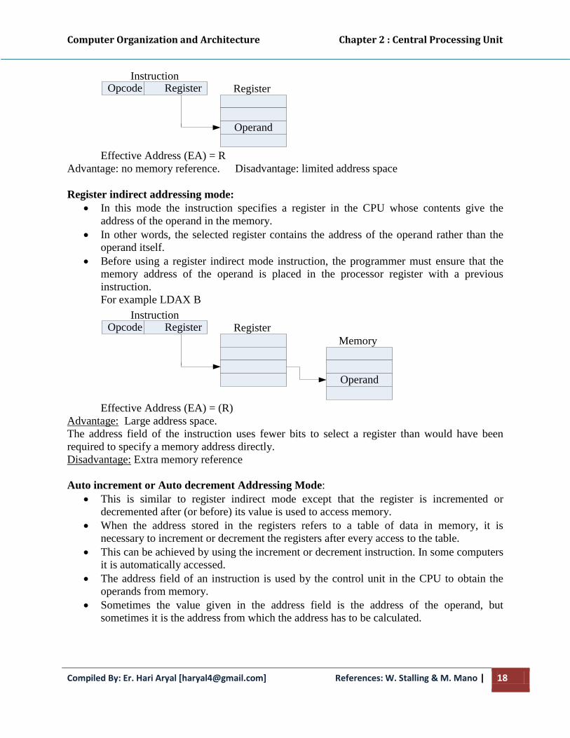
Register indirect addressing mode:
In this mode the instruction specifies a register in the CPU whose contents give the
address of the operand in the memory.
In other words, the selected register contains the address of the operand rather than the
operand itself.
Before using a register indirect mode instruction, the programmer must ensure that the
memory address of the operand is placed in the processor register with a previous
instruction.
For example LDAX B
Opcode RegisterInstruction
Register
Operand
Memory
Effective Address (EA) = (R)
Advantage: Large address space.
The address field of the instruction uses fewer bits to select a register than would have been
required to specify a memory address directly.
Disadvantage: Extra memory reference
Auto increment or Auto decrement Addressing Mode:
This is similar to register indirect mode except that the register is incremented or
decremented after (or before) its value is used to access memory.
When the address stored in the registers refers to a table of data in memory, it is
necessary to increment or decrement the registers after every access to the table.
This can be achieved by using the increment or decrement instruction. In some computers
it is automatically accessed.
The address field of an instruction is used by the control unit in the CPU to obtain the
operands from memory.
Sometimes the value given in the address field is the address of the operand, but
sometimes it is the address from which the address has to be calculated.
Computer Organization and Architecture Chapter 2 : Central Processing Unit
Compiled By: Er. Hari Aryal [[email protected]] References: W. Stalling & M. Mano | 19
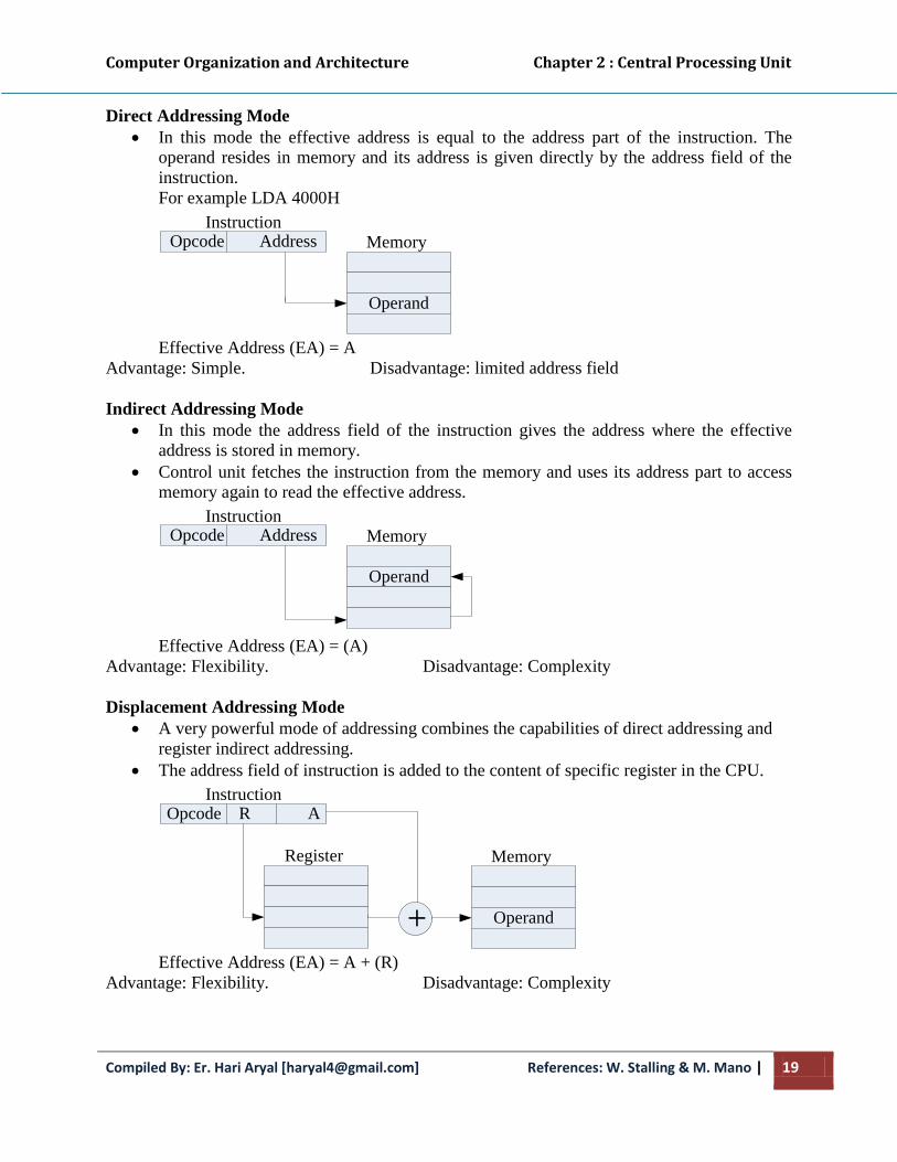
Direct Addressing Mode
In this mode the effective address is equal to the address part of the instruction. The
operand resides in memory and its address is given directly by the address field of the
instruction.
For example LDA 4000H
Opcode AddressInstruction
Operand
Memory
Effective Address (EA) = A
Advantage: Simple. Disadvantage: limited address field
Indirect Addressing Mode
In this mode the address field of the instruction gives the address where the effective
address is stored in memory.
Control unit fetches the instruction from the memory and uses its address part to access
memory again to read the effective address.
Opcode AddressInstruction
Operand
Memory
Effective Address (EA) = (A)
Advantage: Flexibility. Disadvantage: Complexity
Displacement Addressing Mode
A very powerful mode of addressing combines the capabilities of direct addressing and
register indirect addressing.
The address field of instruction is added to the content of specific register in the CPU.
Opcode R AInstruction
Operand
MemoryRegister
+
Effective Address (EA) = A + (R)
Advantage: Flexibility. Disadvantage: Complexity

Computer Organization and Architecture Chapter 2 : Central Processing Unit
Compiled By: Er. Hari Aryal [[email protected]] References: W. Stalling & M. Mano | 20
Relative Addressing Mode
In this mode the content of the program counter (PC) is added to the address part of the
instruction in order to obtain the effective address.
The address part of the instruction is usually a signed number (either a +ve or a –ve
number).
When the number is added to the content of the program counter, the result produces an
effective address whose position in memory is relative to the address of the next
instruction.
Effective Address (EA) = PC + A
Indexed Addressing Mode
In this mode the content of an index register (XR) is added to the address part of the
instruction to obtain the effective address.
The index register is a special CPU register that contains an index value.
Note: If an index-type instruction does not include an address field in its format, the
instruction is automatically converted to the register indirect mode of operation.
Effective Address (EA) = XR + A
Base Register Addressing Mode
In this mode the content of a base register (BR) is added to the address part of the
instruction to obtain the effective address.
This is similar to the indexed addressing mode except that the register is now called a
base register instead of the index register.
The base register addressing mode is used in computers to facilitate the relocation of
programs in memory i.e. when programs and data are moved from one segment of
memory to another.
Effective Address (EA) = BR + A
Stack Addressing Mode
The stack is the linear array of locations. It is some times referred to as push down list or
last in First out (LIFO) queue. The stack pointer is maintained in register.
Instruction
Top of StackImplicit
Effective Address (EA) = TOS

Computer Organization and Architecture Chapter 2 : Central Processing Unit
Compiled By: Er. Hari Aryal [[email protected]] References: W. Stalling & M. Mano | 21
Let us try to evaluate the addressing modes with as example.
Fig: Numerical Example for Addressing Modes
Fig: Tabular list of Numerical Example
Computer Organization and Architecture Chapter 2 : Central Processing Unit
Compiled By: Er. Hari Aryal [[email protected]] References: W. Stalling & M. Mano | 22
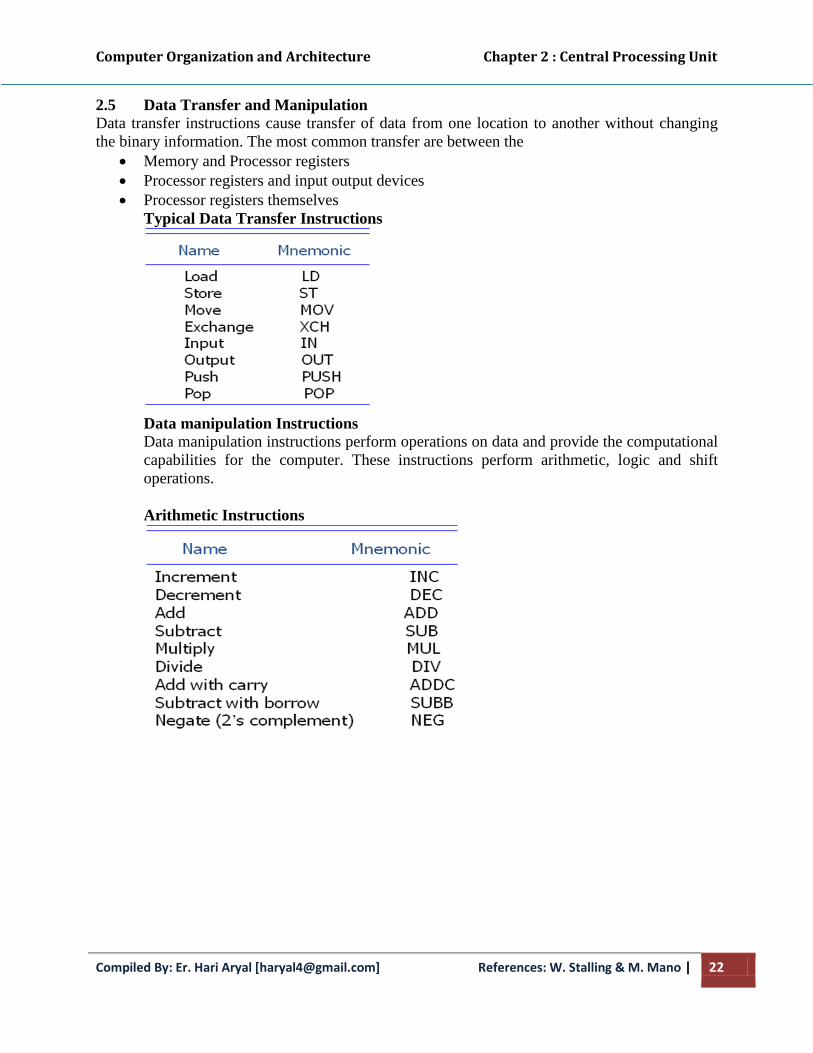
2.5 Data Transfer and Manipulation
Data transfer instructions cause transfer of data from one location to another without changing
the binary information. The most common transfer are between the
Memory and Processor registers
Processor registers and input output devices
Processor registers themselves
Typical Data Transfer Instructions
Data manipulation Instructions
Data manipulation instructions perform operations on data and provide the computational
capabilities for the computer. These instructions perform arithmetic, logic and shift
operations.
Arithmetic Instructions

Computer Organization and Architecture Chapter 2 : Central Processing Unit
Compiled By: Er. Hari Aryal [[email protected]] References: W. Stalling & M. Mano | 23
Logical and Bit Manipulation Instructions
Shift Instructions
Program Control Instructions
The program control instructions provide decision making capabilities and change the
path taken by the program when executed in computer. These instructions specify
conditions for altering the content of the program counter. The change in value of
program counter as a result of execution of program control instruction causes a break in
sequence of instruction execution. Some typical program control instructions are:

Computer Organization and Architecture Chapter 2 : Central Processing Unit
Compiled By: Er. Hari Aryal [[email protected]] References: W. Stalling & M. Mano | 24
Subroutine call and Return
A subroutine call instruction consists of an operation code together with an address that
specifies the beginning of the subroutine. The instruction is executed by performing two
tasks:
The address of the next instruction available in the program counter (the return
address) is stored in a temporary location (stack) so the subroutine knows where
to return.
Control is transferred to the beginning of the subroutine.
The last instruction of every subroutine, commonly called return from subroutine;
transfer the return address from the temporary location into the program counter. This
results in a transfer of program control to the instruction where address was originally
stored in the temporary location.
Interrupt
The interrupt procedure is, in principle, quite similar to a subroutine call except for three
variations:
The interrupt is usually initiated by an external or internal signal rather than from
execution of an instruction.
The address of the interrupt service program is determined by the hardware rather
than from the address field of an instruction.
An interrupt procedure usually stores all the information necessary to define the
state of the CPU rather than storing only the program counter.
2.6 RISC and CISC
Important aspect of computer – design of the instruction set for processor.
Instruction set – determines the way that machine language programs are
constructed.
Early computers – simple and small instruction set, need to minimize the
hardware used.
Advent of IC – cheaper digital software, instructions intended to increase both in
number of complexity.
Many computers – more than 100 or 200 instructions, variety of data types and
large number of addressing modes.
Complex Instruction Set Computers (CISC)
The trend into computer hardware complexity was influenced by various factors:
o Upgrading existing models to provide more customer applications
o Adding instructions that facilitate the translation from high-level language
into machine language programs
o Striving to develop machines that move functions from software
implementation into hardware implementation
A computer with a large number of instructions is classified as a complex
instruction set computer (CISC).
One reason for the trend to provide a complex instruction set is the desire to
simplify the compilation and improve the overall computer performance.
Computer Organization and Architecture Chapter 2 : Central Processing Unit
Compiled By: Er. Hari Aryal [[email protected]] References: W. Stalling & M. Mano | 25
The essential goal of CISC architecture is to attempt to provide a single machine
instruction for each statement that is written in a high-level language.
Examples of CISC architecture are the DEC VAX computer and the IBM 370
computer. Other are 8085, 8086, 80x86 etc.
The major characteristics of CISC architecture
A large number of instructions– typically from 100 to 250 instructions
Some instructions that perform specialized tasks and are used infrequently
A large variety of addressing modes—typically from 5 to 20 different modes
Variable-length instruction formats
Instructions that manipulate operands in memory
Reduced speed due to memory read/write operations
Use of microprogram – special program in control memory of a computer to
perform the timing and sequencing of the microoperations – fetch, decode,
execute etc.
Major complexity in the design of microprogram
No large number of registers – single register set of general purpose and low cost
Reduced Instruction Set Computers (RISC)
A computer uses fewer instructions with simple constructs so they can be executed much
faster within the CPU without having to use memory as often. It is classified as a reduced
instruction set computer (RISC).
RISC concept – an attempt to reduce the execution cycle by simplifying the
instruction set
Small set of instructions – mostly register to register operations and simple
load/store operations for memory access
Each operand – brought into register using load instruction, computations are
done among data in registers and results transferred to memory using store
instruction
Simplify instruction set and encourages the optimization of register
manipulation
May include immediate operands, relative mode etc.
The major characteristics of RISC architecture
Relatively few instructions
Relatively few addressing modes
Memory access limited to load and store instructions
All operations done within the registers of the CPU
Fixed-length, easily decoded instruction format
Single-cycle instruction execution
Hardwired rather than microprogrammed control

Computer Organization and Architecture Chapter 2 : Central Processing Unit
Compiled By: Er. Hari Aryal [[email protected]] References: W. Stalling & M. Mano | 26
Other characteristics attributed to RISC architecture
A relatively large number of registers in the processor unit
Use of overlapped register windows to speed-up procedure call and return
Efficient instruction pipeline – fetch, decode and execute overlap
Compiler support for efficient translation of high-level language programs into
machine language programs
Studies that show improved performance for RISC architecture do not
differentiate between the effects of the reduced instruction set and the effects of a
large register file.
A large number of registers in the processing unit are sometimes associated with
RISC processors.
RISC processors often achieve 2 to 4 times the performance of CISC processors.
RISC uses much less chip space; extra functions like memory management unit or
floating point arithmetic unit can also be placed on same chip. Smaller chips
allow a semiconductor mfg. to place more parts on a single silicon wafer, which
can lower the per chip cost dramatically.
RISC processors are simpler than corresponding CISC processors, they can be
designed more quickly.
Comparison between RISC and CISC Architectures
S.N. RISC CISC
1 Simple instructions taking one cycle Complex instructions taking multiple cycles
2 Only load and store memory references Any instructions may reference memory
3 Heavily pipelined Not/less pipelined
4 Multiple register sets Single register set
5 Complexity is in compiler Complexity is in micro-programming
6 Instructions executed by hardware Instructions interpreted by micro-
programming
7 Fixed format instructions Variable format instructions
8 Few instructions and modes Large instructions and modes

Computer Organization and Architecture Chapter 2 : Central Processing Unit
Compiled By: Er. Hari Aryal [[email protected]] References: W. Stalling & M. Mano | 27
Overlapped register windows
Some computers provide multiple-register banks, and each procedure is allocated its own
bank of registers. This eliminates the need for saving and restoring register values.
Some computers use the memory stack to store the parameters that are needed by the
procedure, but this required a memory access every time the stack is accessed.
A characteristic of some RISC processors is their use of overlapped register windows to
provide the passing of parameters and avoid the need for saving and restoring register
values.
The concept of overlapped register windows is illustrated in below figure.
In general, the organization of register windows will have the following relationships:
Number of global registers = G
Number of local registers in each window = L
Number of registers common to two windows = C
Number of windows = W
The number of registers available for each window is calculated as followed:
Window size = L + 2C + G
The total number of registers needed in the processor is
Register file = (L + C)W + G
Fig: Overlapped Register Window
A total of 74 registers
Global Registers = 10 common to all procedures
64 registers divided into 4 windows A, B, C & D
Each register window = 10 registers local
Two sets of 16 registers common to adjacent procedures

Computer Organization and Architecture Chapter 2 : Central Processing Unit
Compiled By: Er. Hari Aryal [[email protected]] References: W. Stalling & M. Mano | 28
Berkeley RISC I
The Berkeley RISC I is a 32-bit integrated circuit CPU.
o It supports 32-bit address and either 8-, 16-, or 32-bit data.
o It has a 32-bit instruction format and a total of 31 instructions.
o There are three basic addressing modes: Register addressing, immediate operand,
and relative to PC addressing for branch instructions.
o It has a register file of 138 registers; 10 global register and 8 windows of 32
registers in each
o The 32 registers in each window have an organization similar to overlapped
register window.
Fig: Instruction Format of Berkeley RISC I
Above figure shows the 32-bit instruction formats used for register-to-register
instructions and memory access instructions.
Seven of the bits in the operation code specify an operation, and the eighth bit indicates
whether to update the status bits after an ALU operation.
For register-to-register instructions :
o The 5-bit Rd field select one of the 32 registers as a destination for the result of
the operation
o The operation is performed with the data specified in fields Rs and S2.
o Thus the instruction has a three-address format, but the second source may be
either a register or an immediate operand.
For memory access instructions:
o Rs to specify a 32-bit address in a register
o S2 to specify an offset
o Register R0 contains all 0’s, so it can be used in any field to specify a zero
quantity
The third instruction format combines the last three fields to form a 19-bit relative
address Y and is used primarily with the jump and call instructions.
o The COND field replaces the Rd field for jump instructions and is used to specify
one of 16 possible branch conditions.
Computer Organization and Architecture Chapter 2 : Central Processing Unit
Compiled By: Er. Hari Aryal [[email protected]] References: W. Stalling & M. Mano | 29
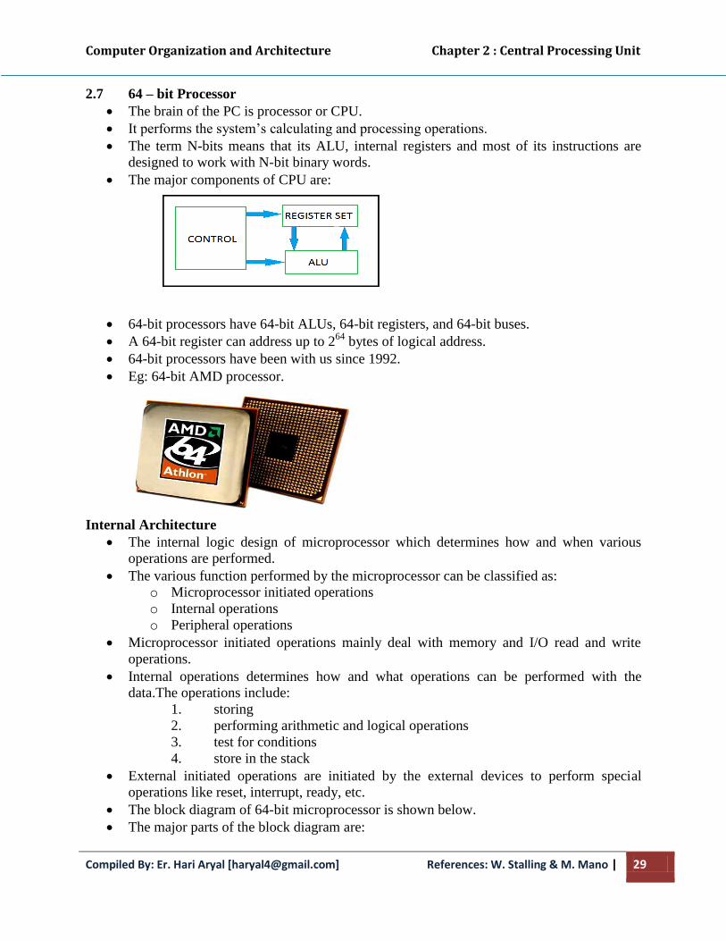
2.7 64 – bit Processor
The brain of the PC is processor or CPU.
It performs the system’s calculating and processing operations.
The term N-bits means that its ALU, internal registers and most of its instructions are
designed to work with N-bit binary words.
The major components of CPU are:
64-bit processors have 64-bit ALUs, 64-bit registers, and 64-bit buses.
A 64-bit register can address up to 264
bytes of logical address.
64-bit processors have been with us since 1992.
Eg: 64-bit AMD processor.
Internal Architecture
The internal logic design of microprocessor which determines how and when various
operations are performed.
The various function performed by the microprocessor can be classified as:
o Microprocessor initiated operations
o Internal operations
o Peripheral operations
Microprocessor initiated operations mainly deal with memory and I/O read and write
operations.
Internal operations determines how and what operations can be performed with the
data.The operations include:
1. storing
2. performing arithmetic and logical operations
3. test for conditions
4. store in the stack
External initiated operations are initiated by the external devices to perform special
operations like reset, interrupt, ready, etc.
The block diagram of 64-bit microprocessor is shown below.
The major parts of the block diagram are:

Computer Organization and Architecture Chapter 2 : Central Processing Unit
Compiled By: Er. Hari Aryal [[email protected]] References: W. Stalling & M. Mano | 30
o General register unit
o Control and decoding unit
o Bus unit
o Cache memory unit
o Floating point register unit
o Issue ports
Fig: Block diagram of 64-bit internal architecture
Architecture Elements
Addressing Modes
General Purpose Registers
Non-modal and modal Instructions
New Instructions in Support of 64-bit
New immediate Instructions
Addressing modes
This addressing mode determines the working environment. i.e 24,32 or 64 bit mode
PSW bits 31 and 32 designate addressing mode (out of 64 bit).
o Addressing modes bits:00=24 bit-mode
Computer Organization and Architecture Chapter 2 : Central Processing Unit
Compiled By: Er. Hari Aryal [[email protected]] References: W. Stalling & M. Mano | 31
01=32 bit-mode
11=64 bit-mode
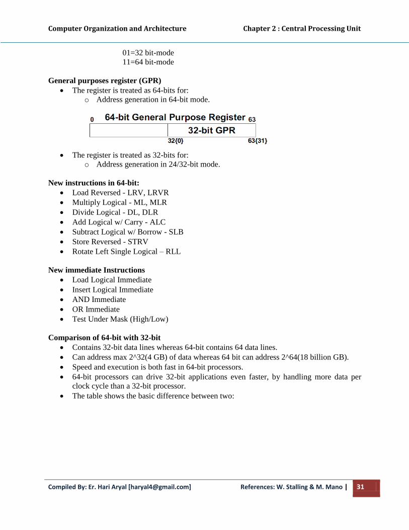
General purposes register (GPR)
The register is treated as 64-bits for:
o Address generation in 64-bit mode.
The register is treated as 32-bits for:
o Address generation in 24/32-bit mode.
New instructions in 64-bit:
Load Reversed - LRV, LRVR
Multiply Logical - ML, MLR
Divide Logical - DL, DLR
Add Logical w/ Carry - ALC
Subtract Logical w/ Borrow - SLB
Store Reversed - STRV
Rotate Left Single Logical – RLL
New immediate Instructions
Load Logical Immediate
Insert Logical Immediate
AND Immediate
OR Immediate
Test Under Mask (High/Low)
Comparison of 64-bit with 32-bit
Contains 32-bit data lines whereas 64-bit contains 64 data lines.
Can address max 2^32(4 GB) of data whereas 64 bit can address 2^64(18 billion GB).
Speed and execution is both fast in 64-bit processors.
64-bit processors can drive 32-bit applications even faster, by handling more data per
clock cycle than a 32-bit processor.
The table shows the basic difference between two:
Computer Organization and Architecture Chapter 2 : Central Processing Unit
Compiled By: Er. Hari Aryal [[email protected]] References: W. Stalling & M. Mano | 32
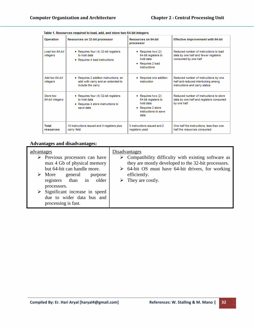
Advantages and disadvantages:
advantages
Previous processors can have
max 4 Gb of physical memory
but 64-bit can handle more.
More general purpose
registers than in older
processors.
Significant increase in speed
due to wider data bus and
processing is fast.
Disadvantages
Compatibility difficulty with existing software as
they are mostly developed to the 32-bit processors.
64-bit OS must have 64-bit drivers, for working
efficiently.
They are costly.
Computer Organization and Architecture Chapter 3 : Control Unit
Compiled By: Er. Hari Aryal [[email protected]] Reference: M. Mano & W. Stallings | 1
Chapter – 3
Control Unit 3.1 Control Memory
The function of the control unit in a digital computer is to initiate sequences of
microoperations.
When the control signals are generated by hardware using conventional logic design
techniques, the control unit is said to be hardwired.
Microprogramming is a second alternative for designing the control unit of a digital
computer.
o The principle of microprogramming is an elegant and systematic method for
controlling the microoperation sequences in a digital computer.
In a bus-organized systems, the control signals that specify microoperations are groups of
bits that select the paths in multiplexers, decoders, and arithmetic logic units.
A control unit whose binary control variables are stored in memory is called a
microprogrammed control unit.
A memory that is part of a control unit is referred to as a control memory.
o Each word in control memory contains within it a microinstruction.
o A sequence of microinstructions constitutes a microprogram.
o Can be either read-only memory(ROM) or writable control memory (dynamic
microprogramming)
A computer that employs a microprogrammed control unit will have two separate
memories:
o A main memory
o A control memory
The general configuration of a microprogrammed control unit is demonstrated in the
block diagram of Fig. 3.1.
o The control memory is assumed to be a ROM, within which all control
information is permanently stored.
o The control address register specifies the address of the microinstruction.
o The control data register holds the microinstruction read from memory.
Thus a microinstruction contains bits for initiating microoperations in the data processor
part and bits that determine the address sequence for the control memory.
Extra Stuff:
Microprogram
Program stored in memory that generates all the control signals required to execute the
instruction set correctly
Consists of microinstructions
Microinstruction
Contains a control word and a sequencing word
Control Word - All the control information required for one clock cycle
Sequencing Word - Information needed to decide the next microinstruction address
Vocabulary to write a microprogram

Computer Organization and Architecture Chapter 3 : Control Unit
Compiled By: Er. Hari Aryal [[email protected]] Reference: M. Mano & W. Stallings | 2
Control Memory (Control Storage: CS)
Storage in the microprogrammed control unit to store the microprogram
Writeable Control Memory(Writeable Control Storage:WCS)
CS whose contents can be modified
Allows the microprogram can be changed
Instruction set can be changed or modified
Dynamic Microprogramming
Computer system whose control unit is implemented with a microprogram in WCS
Microprogram can be changed by a systems programmer or a user
Microrogrammed Sequencer
The next address generator is sometimes called a microprogram sequencer, as it
determines the address sequence that is read from control memory.
Typical functions of a microprogram sequencer are:
o Incrementing the control address register by one
o Loading into the control address register an address from control memory
o Transferring an external address
o Loading an initial address to start the control operations
Pipeline Register
The data register is sometimes called a pipeline register.
o It allows the execution of the microoperations specified by the control word
simultaneously with the generation of the next microinstruction.
This configuration requires a two-phase clock
o The system can operate by applying a single-phase clock to the address register.
Without the control data register
Thus, the control word and next-address information are taken directly
from the control memory.
Advantages
The main advantage of the microprogrammed control is the fact that once the hardware
configuration is established; there should be no need for further hardware or wiring
change.
Most computers based on the reduced instruction set computer (RISC) architecture
concept use hardwired control rather than a control memory with a microprogram.
(Why?)
A Microprogram Control Unit that determines the Microinstruction Address to be executed
in the next clock cycle
In-line Sequencing
Branch
Conditional Branch
Subroutine
Loop
Instruction OP-code mapping

Computer Organization and Architecture Chapter 3 : Control Unit
Compiled By: Er. Hari Aryal [[email protected]] Reference: M. Mano & W. Stallings | 3
External Control
Input Word
Next address information
Fig 3-1: Microprogrammed Control Organization
3.2 Addressing sequencing
Microinstructions are stored in control memory in groups, with each group specifying
a routine.
Each computer instruction has its own microprogram routine in control memory to
generate the microoperations that execute the instruction.
To appreciate the address sequencing in a microprogram control unit:
o An initial address is loaded into the control address register when power is
turned on in the computer.
o This address is usually the address of the first microinstruction that activates
the instruction fetch routine.
o The control memory next must go through the routine that determines the
effective address of the operand.
o The next step is to generate the microoperations that execute the instruction
fetched from memory.
The transformation from the instruction code bits to an address in control memory
where the routine is located is referred to as a mapping process.
The address sequencing capabilities required in a control memory are:
o Incrementing of the control address register
o Unconditional branch or conditional branch, depending on status bit
conditions
o A mapping process from the bits of the instruction to an address for control
memory
o A facility for subroutine call and return
Fig. 3-2 shows a block diagram of a control memory and the associated hardware
needed for selecting the next microinstruction address.
The microinstruction in control memory contains
o a set of bits to initiate microoperations in computer registers
o Other bits to specify the method by which the next address is obtained
Sequencing Capabilities Required in Control Storage
Incrementing of the control address register
Unconditional and conditional branches
A mapping process from the bits of the machine instruction to an address for control
memory
A facility for subroutine call and return
Next
Address
generator
(Sequencer)
Control
Address
Register
Control
Memory
(ROM)
Control
Data
Register
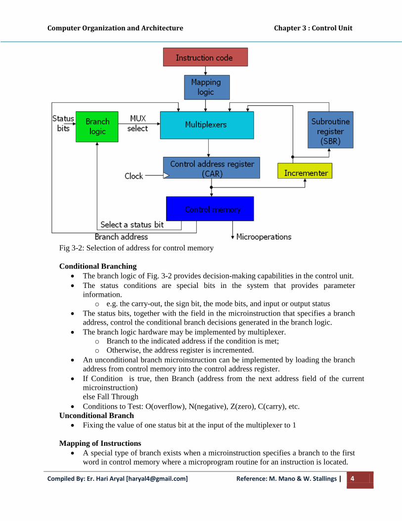
Computer Organization and Architecture Chapter 3 : Control Unit
Compiled By: Er. Hari Aryal [[email protected]] Reference: M. Mano & W. Stallings | 4
Fig 3-2: Selection of address for control memory
Conditional Branching
The branch logic of Fig. 3-2 provides decision-making capabilities in the control unit.
The status conditions are special bits in the system that provides parameter
information.
o e.g. the carry-out, the sign bit, the mode bits, and input or output status
The status bits, together with the field in the microinstruction that specifies a branch
address, control the conditional branch decisions generated in the branch logic.
The branch logic hardware may be implemented by multiplexer.
o Branch to the indicated address if the condition is met;
o Otherwise, the address register is incremented.
An unconditional branch microinstruction can be implemented by loading the branch
address from control memory into the control address register.
If Condition is true, then Branch (address from the next address field of the current
microinstruction)
else Fall Through
Conditions to Test: O(overflow), N(negative), Z(zero), C(carry), etc.
Unconditional Branch
Fixing the value of one status bit at the input of the multiplexer to 1
Mapping of Instructions
A special type of branch exists when a microinstruction specifies a branch to the first
word in control memory where a microprogram routine for an instruction is located.

Computer Organization and Architecture Chapter 3 : Control Unit
Compiled By: Er. Hari Aryal [[email protected]] Reference: M. Mano & W. Stallings | 5
The status bits for this type of branch are the bits in the operation code part of the
instruction.
One simple mapping process that converts the 4-bit operation code to a 7-bit address
for control memory is shown in Fig. 3-3.
o Placing a 0 in the most significant bit of the address
o Transferring the four operation code bits
o Clearing the two least significant bits of the control address register
This provides for each computer instruction a microprogram routine with a capacity
of four microinstructions.
o If the routine needs more than four microinstructions, it can use addresses
1000000 through 1111111.
o If it uses fewer than four microinstructions, the unused memory locations
would be available for other routines.
One can extend this concept to a more general mapping rule by using a ROM or
programmable logic device (PLD) to specify the mapping function.
Fig 3-3: Mapping from instruction code to microinstruction address
Fig 3-3 (a): Direct mapping
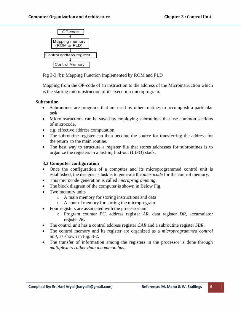
Computer Organization and Architecture Chapter 3 : Control Unit
Compiled By: Er. Hari Aryal [[email protected]] Reference: M. Mano & W. Stallings | 6
Fig 3-3 (b): Mapping Function Implemented by ROM and PLD
Mapping from the OP-code of an instruction to the address of the Microinstruction which
is the starting microinstruction of its execution microprogram.
Subroutine
Subroutines are programs that are used by other routines to accomplish a particular
task.
Microinstructions can be saved by employing subroutines that use common sections
of microcode.
e.g. effective address computation
The subroutine register can then become the source for transferring the address for
the return to the main routine.
The best way to structure a register file that stores addresses for subroutines is to
organize the registers in a last-in, first-out (LIFO) stack.
3.3 Computer configuration
Once the configuration of a computer and its microprogrammed control unit is
established, the designer’s task is to generate the microcode for the control memory.
This microcode generation is called microprogramming.
The block diagram of the computer is shown in Below Fig.
Two memory units
o A main memory for storing instructions and data
o A control memory for storing the microprogram
Four registers are associated with the processor unit
o Program counter PC, address register AR, data register DR, accumulator
register AC
The control unit has a control address register CAR and a subroutine register SBR.
The control memory and its register are organized as a microprogrammed control
unit, as shown in Fig. 3-2.
The transfer of information among the registers in the processor is done through
multiplexers rather than a common bus.
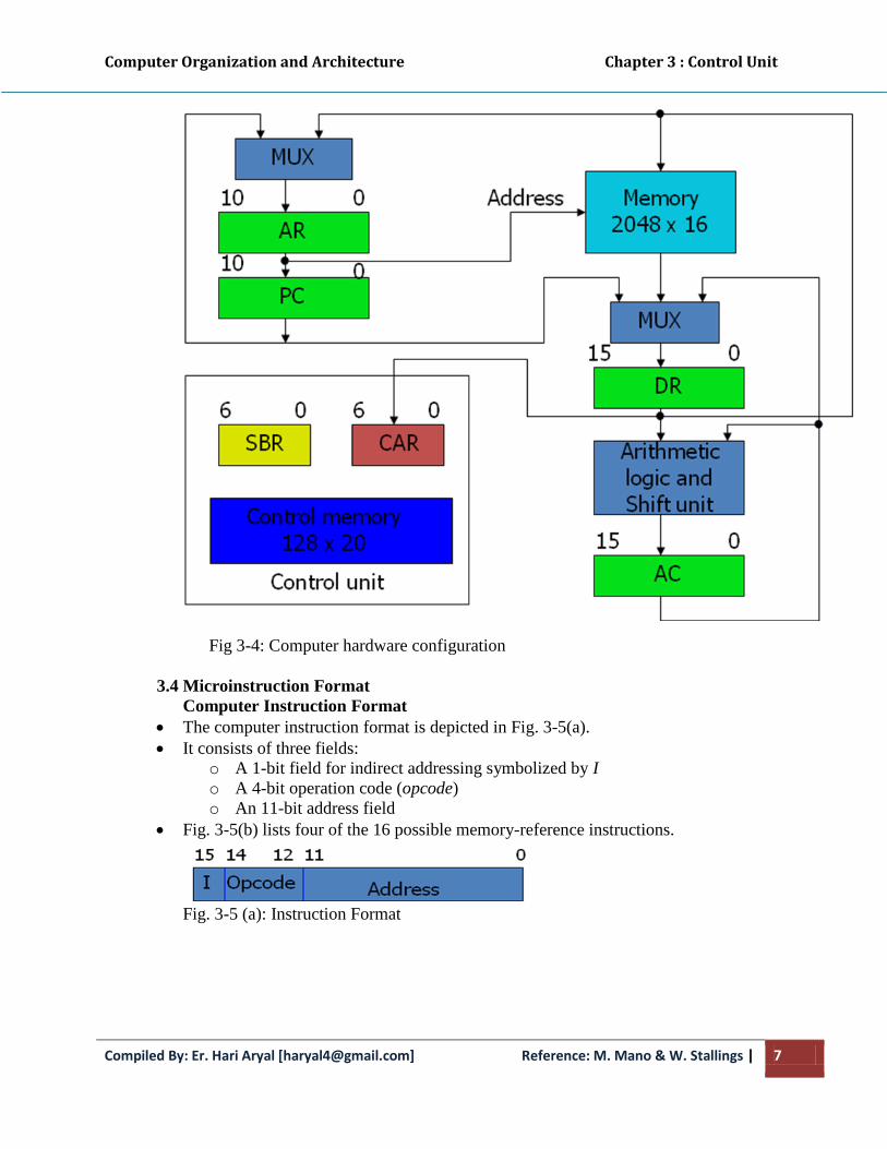
Computer Organization and Architecture Chapter 3 : Control Unit
Compiled By: Er. Hari Aryal [[email protected]] Reference: M. Mano & W. Stallings | 7
Fig 3-4: Computer hardware configuration
3.4 Microinstruction Format
Computer Instruction Format
The computer instruction format is depicted in Fig. 3-5(a).
It consists of three fields:
o A 1-bit field for indirect addressing symbolized by I
o A 4-bit operation code (opcode)
o An 11-bit address field
Fig. 3-5(b) lists four of the 16 possible memory-reference instructions.
Fig. 3-5 (a): Instruction Format
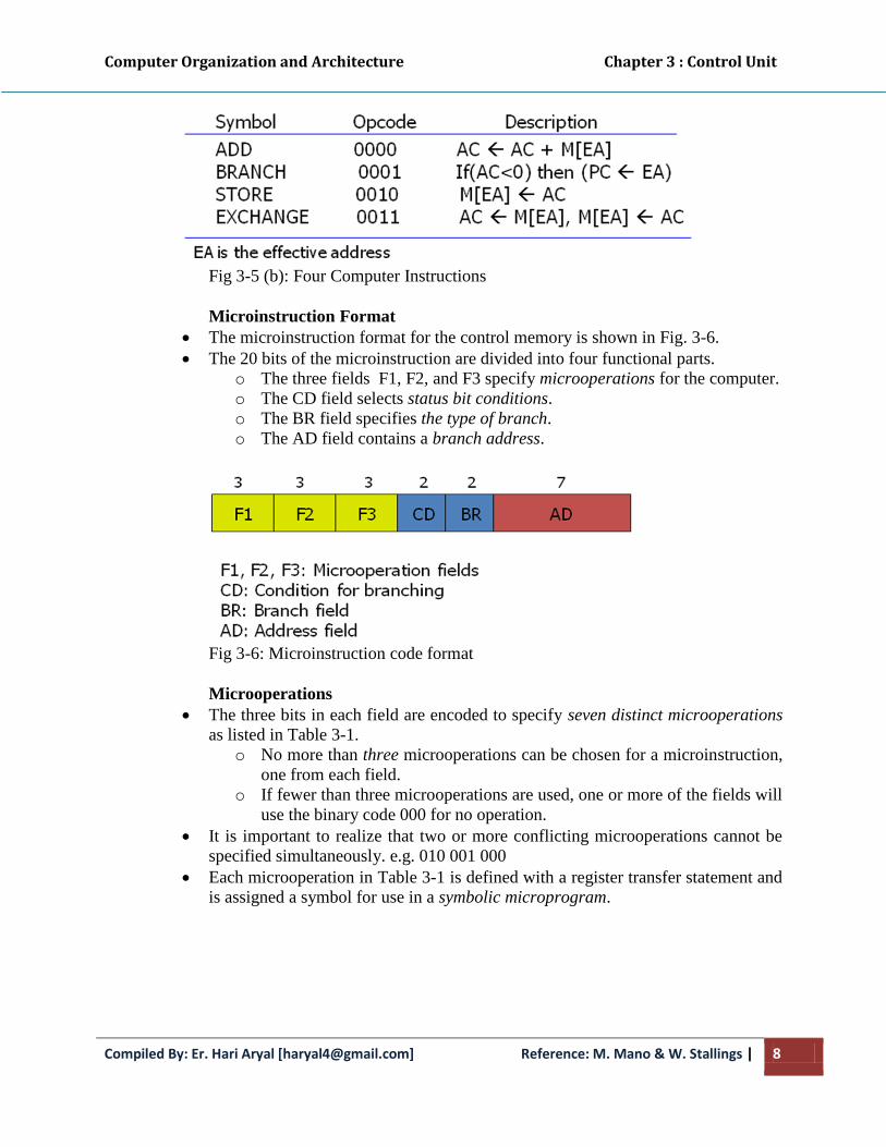
Computer Organization and Architecture Chapter 3 : Control Unit
Compiled By: Er. Hari Aryal [[email protected]] Reference: M. Mano & W. Stallings | 8
Fig 3-5 (b): Four Computer Instructions
Microinstruction Format
The microinstruction format for the control memory is shown in Fig. 3-6.
The 20 bits of the microinstruction are divided into four functional parts.
o The three fields F1, F2, and F3 specify microoperations for the computer.
o The CD field selects status bit conditions.
o The BR field specifies the type of branch.
o The AD field contains a branch address.
Fig 3-6: Microinstruction code format
Microoperations
The three bits in each field are encoded to specify seven distinct microoperations
as listed in Table 3-1.
o No more than three microoperations can be chosen for a microinstruction,
one from each field.
o If fewer than three microoperations are used, one or more of the fields will
use the binary code 000 for no operation.
It is important to realize that two or more conflicting microoperations cannot be
specified simultaneously. e.g. 010 001 000
Each microoperation in Table 3-1 is defined with a register transfer statement and
is assigned a symbol for use in a symbolic microprogram.

Computer Organization and Architecture Chapter 3 : Control Unit
Compiled By: Er. Hari Aryal [[email protected]] Reference: M. Mano & W. Stallings | 9

Computer Organization and Architecture Chapter 3 : Control Unit
Compiled By: Er. Hari Aryal [[email protected]] Reference: M. Mano & W. Stallings | 10
Table 3-1 : Symbols and Binary code for Microinstruction Fields
Condition and Branch Field
The CD field consists of two bits which are encoded to specify four status bit
conditions as listed in Table 3-1.
The BR field consists of two bits. It is used, in conjunction with the address
field AD, to choose the address of the next microinstruction.
o The jump and call operations depend on the value of the CD field.
o The two operations are identical except that a call microinstruction stores
the return address in the subroutine register SBR.
o Note that the last two conditions in the BR field are independent of the
values in the CD and AD fields.
3.5 Symbolic Microinstructions
The symbols defined in Table 3-1 cab be used to specify microinstructions in
symbolic form.
Symbols are used in microinstructions as in assembly language
The simplest and most straightforward way to formulate an assembly
language for a microprogram is to define symbols for each field of the
microinstruction and to give users the capability for defining their own
symbolic addresses.
A symbolic microprogram can be translated into its binary equivalent by a
microprogram assembler.

Computer Organization and Architecture Chapter 3 : Control Unit
Compiled By: Er. Hari Aryal [[email protected]] Reference: M. Mano & W. Stallings | 11
Sample Format
Five fields: label; micro-ops; CD; BR; AD
The label field: may be empty or it may specify a symbolic address
terminated with a colon
The microoperations field: of one, two, or three symbols separated by
commas , the NOP symbol is used when the microinstruction has no
microoperations
The CD field: one of the letters {U, I, S, Z} can be chosen where
U: Unconditional Branch
I: Indirect address bit
S: Sign of AC
Z: Zero value in AC
The BR field: contains one of the four symbols {JMP, CALL, RET,
MAP}
The AD field: specifies a value for the address field of the
microinstruction with one of {Symbolic address, NEXT, empty}
o When the BR field contains a RET or MAP symbol, the AD field
is left empty
Fetch Subroutine
During FETCH, Read an instruction from memory and decode the instruction and update PC.
The first 64 words are to be occupied by the routines for the 16 instructions.
The last 64 words may be used for any other purpose.
o A convenient starting location for the fetch routine is address 64.
The three microinstructions that constitute the fetch routine have been listed in three
different representations.
o The register transfer representation:
o The symbolic representation:
o The binary representation:
3.6 Symbolic Microprogram
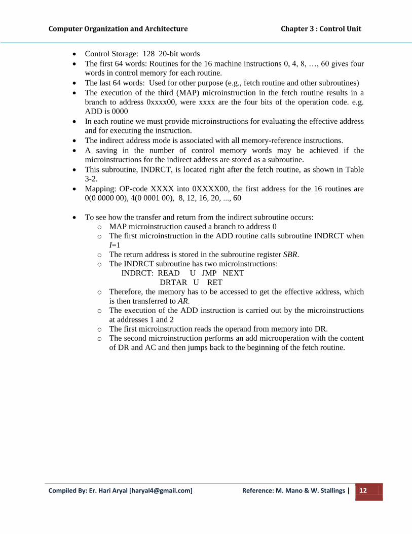
Computer Organization and Architecture Chapter 3 : Control Unit
Compiled By: Er. Hari Aryal [[email protected]] Reference: M. Mano & W. Stallings | 12
Control Storage: 128 20-bit words
The first 64 words: Routines for the 16 machine instructions 0, 4, 8, …, 60 gives four
words in control memory for each routine.
The last 64 words: Used for other purpose (e.g., fetch routine and other subroutines)
The execution of the third (MAP) microinstruction in the fetch routine results in a
branch to address 0xxxx00, were xxxx are the four bits of the operation code. e.g.
ADD is 0000
In each routine we must provide microinstructions for evaluating the effective address
and for executing the instruction.
The indirect address mode is associated with all memory-reference instructions.
A saving in the number of control memory words may be achieved if the
microinstructions for the indirect address are stored as a subroutine.
This subroutine, INDRCT, is located right after the fetch routine, as shown in Table
3-2.
Mapping: OP-code XXXX into 0XXXX00, the first address for the 16 routines are
0(0 0000 00), 4(0 0001 00), 8, 12, 16, 20, ..., 60
To see how the transfer and return from the indirect subroutine occurs:
o MAP microinstruction caused a branch to address 0
o The first microinstruction in the ADD routine calls subroutine INDRCT when
I=1
o The return address is stored in the subroutine register SBR.
o The INDRCT subroutine has two microinstructions:
INDRCT: READ U JMP NEXT
DRTAR U RET
o Therefore, the memory has to be accessed to get the effective address, which
is then transferred to AR.
o The execution of the ADD instruction is carried out by the microinstructions
at addresses 1 and 2
o The first microinstruction reads the operand from memory into DR.
o The second microinstruction performs an add microoperation with the content
of DR and AC and then jumps back to the beginning of the fetch routine.

Computer Organization and Architecture Chapter 3 : Control Unit
Compiled By: Er. Hari Aryal [[email protected]] Reference: M. Mano & W. Stallings | 13
Table 3-2: Symbolic Microprogram for Control Memory (Partial)
Binary Microprogram
The symbolic microprogram must be translated to binary either by means of an
assembler program or by the user if the microprogram is simple.
The equivalent binary form of the microprogram is listed in Table 7-3.
Even though address 3 is not used, some binary value, e.g. all 0’s, must be
specified for each word in control memory.
However, if some unforeseen error occurs, or if a noise signal sets CAR to the
value of 3, it will be wise to jump to address 64.

Computer Organization and Architecture Chapter 3 : Control Unit
Compiled By: Er. Hari Aryal [[email protected]] Reference: M. Mano & W. Stallings | 14
Table 3-3: Binary Microprogram for control memory (Partial)
Control Memory
When a ROM is used for the control memory,the microprogram binary list
provides the truth table for fabricating the unit.
o To modify the instruction set of the computer, it is necessary to generate a
new microprogram and mask a new ROM.
The advantage of employing a RAM for the control memory is that the
microprogram can be altered simply by writing a new pattern of 1’s and 0’s
without resorting to hardware procedure.
However, most microprogram systems use a ROM for the control memory
because it is cheaper and faster than a RAM.
3.7 Control Unit Operation
Microoperations
A computer executes a program consisting instructions. Each instruction is
made up of shorter sub-cycles as fetch, indirect, execute cycle, interrupt.
Performance of each cycle has a number of shorter operations called micro-
operations.
Called so because each step is very simple and does very little.
Thus micro-operations are functional atomic operation of CPU.

Computer Organization and Architecture Chapter 3 : Control Unit
Compiled By: Er. Hari Aryal [[email protected]] Reference: M. Mano & W. Stallings | 15
Hence events of any instruction cycle can be described as a sequence of
micro-operations
Fig 3-7: Constituent Elements of Program Execution
Steps leading to characterization of CU
Define basic elements of processor
Describe micro-operations processor performs
Determine functions control unit must perform
Types of Micro-operation
Transfer data between registers
Transfer data from register to external interface
Transfer data from external interface to register
Perform arithmetic/logical ops with register for i/p, o/p
Functions of Control Unit
Sequencing
Causing the CPU to step through a series of micro-operations
Execution
Causing the performance of each micro-op
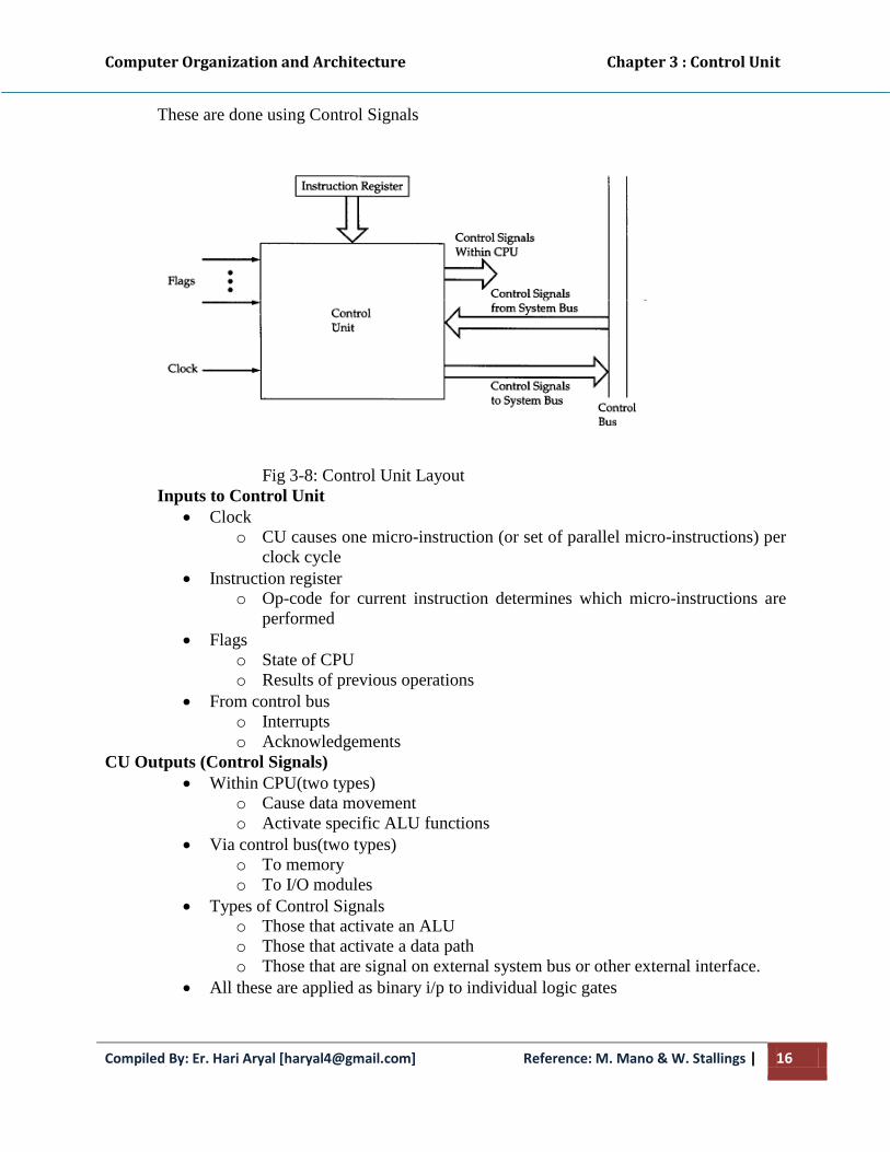
Computer Organization and Architecture Chapter 3 : Control Unit
Compiled By: Er. Hari Aryal [[email protected]] Reference: M. Mano & W. Stallings | 16
These are done using Control Signals
Fig 3-8: Control Unit Layout
Inputs to Control Unit
Clock
o CU causes one micro-instruction (or set of parallel micro-instructions) per
clock cycle
Instruction register
o Op-code for current instruction determines which micro-instructions are
performed
Flags
o State of CPU
o Results of previous operations
From control bus
o Interrupts
o Acknowledgements
CU Outputs (Control Signals)
Within CPU(two types)
o Cause data movement
o Activate specific ALU functions
Via control bus(two types)
o To memory
o To I/O modules
Types of Control Signals
o Those that activate an ALU
o Those that activate a data path
o Those that are signal on external system bus or other external interface.
All these are applied as binary i/p to individual logic gates

Computer Organization and Architecture Chapter 3 : Control Unit
Compiled By: Er. Hari Aryal [[email protected]] Reference: M. Mano & W. Stallings | 17
Hardwired Implementation
In this implementation, CU is essentially a combinational circuit. Its i/p signals
are transformed into set of o/p logic signal which are control signals.
Control unit inputs
Flags and control bus
o Each bit means something
Instruction register
o Op-code causes different control signals for each different instruction
o Unique logic for each op-code
o Decoder takes encoded input and produces single output
o Each decoder i/p will activate a single unique o/p
Clock
o Repetitive sequence of pulses
o Useful for measuring duration of micro-ops
o Must be long enough to allow signal propagation along data paths and
through processor circuitry
o Different control signals at different times within instruction cycle
o Need a counter as i/p to control unit with different control signals being
used for t1, t2 etc.
o At end of instruction cycle, counter is re-initialised
Fig 3-9: Control Unit With Decoded Input

Computer Organization and Architecture Chapter 3 : Control Unit
Compiled By: Er. Hari Aryal [[email protected]] Reference: M. Mano & W. Stallings | 18
Implementation
For each control signal, a Boolean expression of that signal as a function of the
inputs is derived
With that the combinatorial circuit is realized as control unit.
Problems With Hard Wired Designs
Complex sequencing & micro-operation logic
Difficult to design and test
Inflexible design
Difficult to add new instructions
Micro-programmed Implementation
An alternative to hardwired CU
Common in contemporary CISC processors
Use sequences of instructions to perform control operations performed by micro
operations called micro-programming or firmware
Fig 3-10: Microprogrammed Control Unit
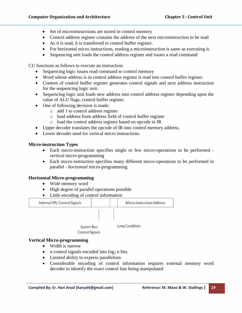
Computer Organization and Architecture Chapter 3 : Control Unit
Compiled By: Er. Hari Aryal [[email protected]] Reference: M. Mano & W. Stallings | 19
Set of microinsrurctions are stored in control memory
Control address register contains the address of the next microinstruction to be read
As it is read, it is transferred to control buffer register.
For horizontal micro instructions, reading a microinstruction is same as executing it.
Sequencing unit loads the control address register and issues a read command
CU functions as follows to execute an instruction:
Sequencing logic issues read command to control memory
Word whose address is in control address register is read into control buffer register.
Content of control buffer register generates control signals and next address instruction
for the sequencing logic unit.
Sequencing logic unit loads new address into control address register depending upon the
value of ALU flags, control buffer register.
One of following decision is made:
o add 1 to control address register
o load address from address field of control buffer register
o load the control address register based on opcode in IR
Upper decoder translates the opcode of IR into control memory address.
Lower decoder used for veritcal micro instructions.
Micro-instruction Types
Each micro-instruction specifies single or few micro-operations to be performed -
vertical micro-programming
Each micro-instruction specifies many different micro-operations to be performed in
parallel - horizontal micro-programming
Horizontal Micro-programming
Wide memory word
High degree of parallel operations possible
Little encoding of control information
Vertical Micro-programming
Width is narrow
n control signals encoded into log2 n bits
Limited ability to express parallelism
Considerable encoding of control information requires external memory word
decoder to identify the exact control line being manipulated
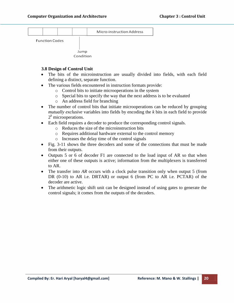
Computer Organization and Architecture Chapter 3 : Control Unit
Compiled By: Er. Hari Aryal [[email protected]] Reference: M. Mano & W. Stallings | 20
3.8 Design of Control Unit
The bits of the microinstruction are usually divided into fields, with each field
defining a distinct, separate function.
The various fields encountered in instruction formats provide:
o Control bits to initiate microoperations in the system
o Special bits to specify the way that the next address is to be evaluated
o An address field for branching
The number of control bits that initiate microoperations can be reduced by grouping
mutually exclusive variables into fields by encoding the k bits in each field to provide
2k microoperations.
Each field requires a decoder to produce the corresponding control signals.
o Reduces the size of the microinstruction bits
o Requires additional hardware external to the control memory
o Increases the delay time of the control signals
Fig. 3-11 shows the three decoders and some of the connections that must be made
from their outputs.
Outputs 5 or 6 of decoder F1 are connected to the load input of AR so that when
either one of these outputs is active; information from the multiplexers is transferred
to AR.
The transfer into AR occurs with a clock pulse transition only when output 5 (from
DR (0-10) to AR i.e. DRTAR) or output 6 (from PC to AR i.e. PCTAR) of the
decoder are active.
The arithmetic logic shift unit can be designed instead of using gates to generate the
control signals; it comes from the outputs of the decoders.

Computer Organization and Architecture Chapter 3 : Control Unit
Compiled By: Er. Hari Aryal [[email protected]] Reference: M. Mano & W. Stallings | 21
Fig 3-11: Decoding of Microoperation fields
Microprogram Sequencer
The basic components of a microprogrammed control unit are the control memory and
the circuits that select the next address.
The address selection part is called a microprogram sequencer.
A microprogram sequencer can be constructed with digital functions to suit a particular
application.
To guarantee a wide range of acceptability, an integrated circuit sequencer must provide
an internal organization that can be adapted to a wide range of application.
The purpose of a microprogram sequencer is to present an address to the control memory
so that a microinstruction may be read and executed.
The block diagram of the microprogram sequencer is shown in Fig. 3-12.
o The control memory is included to show the interaction between the sequencer
and the attached to it.
o There are two multiplexers in the circuit; first multiplexer selects an address from
one of the four sources and routes to CAR, second multiplexer tests the value of
the selected status bit and result is applied to an input logic circuit.
o The output from CAR provides the address for control memory, contents of CAR
incremented and applied to one of the multiplexers input and to the SBR.

Computer Organization and Architecture Chapter 3 : Control Unit
Compiled By: Er. Hari Aryal [[email protected]] Reference: M. Mano & W. Stallings | 22
o Although the diagram shows a single subroutine register, a typical sequencer will
have a register stack about four to eight levels deep. In this way, a push, pop
operation and stack pointer operates for subroutine call and return instructions.
o The CD (Condition) field of the microinstruction selects one of the status bits in
the second multiplexer.
o The Test variable (either 1 or 0) i.e. T value together with the two bits from the
BR (Branch) field go to an input logic circuit.
o The input logic circuit determines the type of the operation.
Fig 3-12: Microprom Sequencer for a Control Memory
Design of Input Logic
The input logic in a particular sequencer will determine the type of operations that are
available in the unit.
Typical sequencer operations are: increment, branch or jump, call and return from
subroutine, load an external address, push or pop the stack, and other address
sequencing operations.

Computer Organization and Architecture Chapter 3 : Control Unit
Compiled By: Er. Hari Aryal [[email protected]] Reference: M. Mano & W. Stallings | 23
Based on the function listed in each entry was defined in Table 3-1, the truth table for the input
logic circuit is shown in Table 3-4.
Therefore, the simplified Boolean functions for the input logic circuit can be given as:
TIIL
TIIIS
IS
01
1010
11
Table 3-4: Input logic truth table for microprogram sequencer
o The bit values for S1 and S0 are determined from the stated function and the path in the
multiplexer that establishes the required transfer.
o Note that the incrementer circuit in the sequencer of Fig. 7-12 is not a counter constructed
with flip-flops but rather a combinational circuit constructed with gates.
Computer Organization and Architecture Chapter 4 : Pipeline and Vector processing
Compiled By: Er. Hari Aryal [[email protected]] Reference: W. Stallings | 1
Chapter – 4
Pipeline and Vector Processing
4.1 Pipelining
Pipelining is a technique of decomposing a sequential process into
suboperations, with each subprocess being executed in a special dedicated
segment that operates concurrently with all other segments.
The overlapping of computation is made possible by associating a register
with each segment in the pipeline.
The registers provide isolation between each segment so that each can operate
on distinct data simultaneously.
Perhaps the simplest way of viewing the pipeline structure is to imagine that
each segment consists of an input register followed by a combinational
circuit.
o The register holds the data.
o The combinational circuit performs the suboperation in the particular
segment.
A clock is applied to all registers after enough time has elapsed to perform all
segment activity.
The pipeline organization will be demonstrated by means of a simple
example.
o To perform the combined multiply and add operations with a stream of
numbers
Ai * Bi + Ci for i = 1, 2, 3, …, 7
Each suboperation is to be implemented in a segment within a pipeline.
R1 Ai, R2 Bi Input Ai and Bi
R3 R1 * R2, R4 Ci Multiply and input Ci
R5 R3 + R4 Add Ci to product
Each segment has one or two registers and a combinational circuit as shown in
Fig. 9-2.
The five registers are loaded with new data every clock pulse. The effect of
each clock is shown in Table 4-1.

Computer Organization and Architecture Chapter 4 : Pipeline and Vector processing
Compiled By: Er. Hari Aryal [[email protected]] Reference: W. Stallings | 2
Fig 4-1: Example of pipeline processing
Table 4-1: Content of Registers in Pipeline Example
General Considerations
Any operation that can be decomposed into a sequence of suboperations of
about the same complexity can be implemented by a pipeline processor.
The general structure of a four-segment pipeline is illustrated in Fig. 4-2.
We define a task as the total operation performed going through all the
segments in the pipeline.
The behavior of a pipeline can be illustrated with a space-time diagram.
o It shows the segment utilization as a function of time.

Computer Organization and Architecture Chapter 4 : Pipeline and Vector processing
Compiled By: Er. Hari Aryal [[email protected]] Reference: W. Stallings | 3
Fig 4-2: Four Segment Pipeline
The space-time diagram of a four-segment pipeline is demonstrated in Fig. 4-3.
Where a k-segment pipeline with a clock cycle time tp is used to execute n tasks.
o The first task T1 requires a time equal to ktp to complete its operation.
o The remaining n-1 tasks will be completed after a time equal to (n-1)tp
o Therefore, to complete n tasks using a k-segment pipeline requires k+(n-1)
clock cycles.
Consider a nonpipeline unit that performs the same operation and takes a time
equal to tn to complete each task.
o The total time required for n tasks is ntn.
Fig 4-3: Space-time diagram for pipeline
The speedup of a pipeline processing over an equivalent non-pipeline processing
is defined by the ratio S = ntn/(k+n-1)tp .
If n becomes much larger than k-1, the speedup becomes S = tn/tp.
If we assume that the time it takes to process a task is the same in the pipeline and
non-pipeline circuits, i.e., tn = ktp, the speedup reduces to S=ktp/tp=k.
This shows that the theoretical maximum speed up that a pipeline can provide is
k, where k is the number of segments in the pipeline.
To duplicate the theoretical speed advantage of a pipeline process by means of
multiple functional units, it is necessary to construct k identical units that will be
operating in parallel.
This is illustrated in Fig. 4-4, where four identical circuits are connected in
parallel.
Instead of operating with the input data in sequence as in a pipeline, the parallel
circuits accept four input data items simultaneously and perform four tasks at the
same time.

Computer Organization and Architecture Chapter 4 : Pipeline and Vector processing
Compiled By: Er. Hari Aryal [[email protected]] Reference: W. Stallings | 4
Fig 4-4: Multiple functional units in parallel
There are various reasons why the pipeline cannot operate at its maximum
theoretical rate.
o Different segments may take different times to complete their sub
operation.
o It is not always correct to assume that a non pipe circuit has the same time
delay as that of an equivalent pipeline circuit.
There are two areas of computer design where the pipeline organization is
applicable.
o Arithmetic pipeline
o Instruction pipeline
4.2 Parallel Processing
Parallel processing is a term used to denote a large class of techniques that
are used to provide simultaneous data-processing tasks for the purpose of
increasing the computational speed of a computer system.
The purpose of parallel processing is to speed up the computer processing
capability and increase its throughput, that is, the amount of processing that
can be accomplished during a given interval of time.
The amount of hardware increases with parallel processing, and with it, the
cost of the system increases.
Parallel processing can be viewed from various levels of complexity.
o At the lowest level, we distinguish between parallel and serial
operations by the type of registers used. e.g. shift registers and
registers with parallel load
o At a higher level, it can be achieved by having a multiplicity of
functional units that perform identical or different operations
simultaneously.
Fig. 4-5 shows one possible way of separating the execution unit into eight
functional units operating in parallel.
o A multifunctional organization is usually associated with a complex
control unit to coordinate all the activities among the various
components.
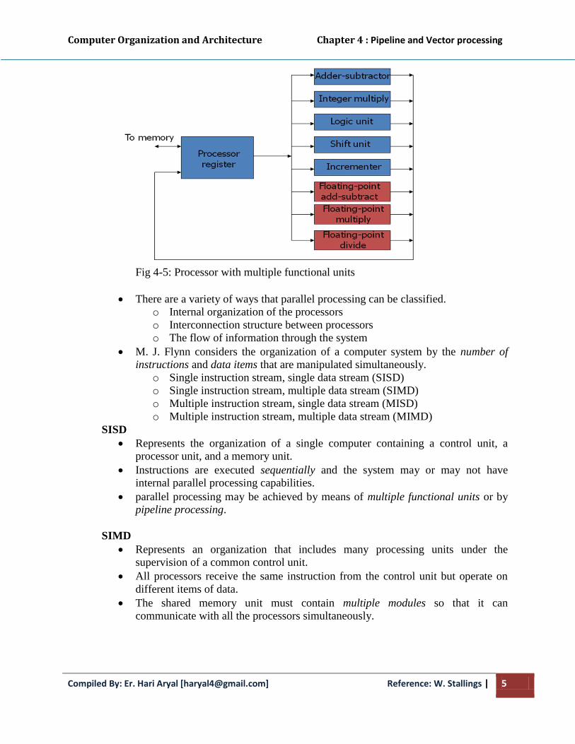
Computer Organization and Architecture Chapter 4 : Pipeline and Vector processing
Compiled By: Er. Hari Aryal [[email protected]] Reference: W. Stallings | 5
Fig 4-5: Processor with multiple functional units
There are a variety of ways that parallel processing can be classified.
o Internal organization of the processors
o Interconnection structure between processors
o The flow of information through the system
M. J. Flynn considers the organization of a computer system by the number of
instructions and data items that are manipulated simultaneously.
o Single instruction stream, single data stream (SISD)
o Single instruction stream, multiple data stream (SIMD)
o Multiple instruction stream, single data stream (MISD)
o Multiple instruction stream, multiple data stream (MIMD)
SISD
Represents the organization of a single computer containing a control unit, a
processor unit, and a memory unit.
Instructions are executed sequentially and the system may or may not have
internal parallel processing capabilities.
parallel processing may be achieved by means of multiple functional units or by
pipeline processing.
SIMD
Represents an organization that includes many processing units under the
supervision of a common control unit.
All processors receive the same instruction from the control unit but operate on
different items of data.
The shared memory unit must contain multiple modules so that it can
communicate with all the processors simultaneously.

Computer Organization and Architecture Chapter 4 : Pipeline and Vector processing
Compiled By: Er. Hari Aryal [[email protected]] Reference: W. Stallings | 6
MISD & MIMD
MISD structure is only of theoretical interest since no practical system has been
constructed using this organization.
MIMD organization refers to a computer system capable of processing several
programs at the same time. e.g. multiprocessor and multicomputer system
Flynn’s classification depends on the distinction between the performance of the
control unit and the data-processing unit.
It emphasizes the behavioral characteristics of the computer system rather than its
operational and structural interconnections.
One type of parallel processing that does not fit Flynn’s classification is
pipelining.
We consider parallel processing under the following main topics:
o Pipeline processsing
Is an implementation technique where arithmetic suboperations or
the phases of a computer instruction cycle overlap in execution.
o Vector processing
Deals with computations involving large vectors and matrices.
o Array processing
Perform computations on large arrays of data.
4.3 Arithmetic Pipeline
Pipeline arithmetic units are usually found in very high speed computers
o Floating–point operations, multiplication of fixed-point numbers, and
similar computations in scientific problem
Floating–point operations are easily decomposed into sub operations.
An example of a pipeline unit for floating-point addition and subtraction is
showed in the following:
o The inputs to the floating-point adder pipeline are two normalized
floating-point binary number
b
a
BY
AX
2
2
o A and B are two fractions that represent the mantissas
o a and b are the exponents
The floating-point addition and subtraction can be performed in four
segments, as shown in Fig. 4-6.
The suboperations that are performed in the four segments are:
o Compare the exponents
The larger exponent is chosen as the exponent of the result.
o Align the mantissas
The exponent difference determines how many times the
mantissa associated with the smaller exponent must be shifted
to the right.
o Add or subtract the mantissas
o Normalize the result
Computer Organization and Architecture Chapter 4 : Pipeline and Vector processing
Compiled By: Er. Hari Aryal [[email protected]] Reference: W. Stallings | 7
When an overflow occurs, the mantissa of the sum or
difference is shifted right and the exponent incremented by
one.
If an underflow occurs, the number of leading zeros in the
mantissa determines the number of left shifts in the mantissa
and the number that must be subtracted from the exponent.
The following numerical example may clarify the suboperations performed in
each segment.
The comparator, shift, adder, subtractor, incrementer, and decrementer in the
floating-point pipeline are implemented with combinational circuits.
Suppose that the time delays of the four segments are t1=60ns, t2=70ns,
t3=100ns, t4=80ns, and the interface registers have a delay of tr=10ns
o Pipeline floating-point arithmetic delay: tp=t3+tr=110ns
o Nonpipeline floating-point arithmetic delay: tn=t1+t2+t3+t4+tr=320ns
o Speedup: 320/110=2.9
Fig 4-6: Pipeline for floating point addition and subtraction
4.4 Instruction Pipeline
Pipeline processing can occur not only in the data stream but in the
instruction as well.
Consider a computer with an instruction fetch unit and an instruction
execution unit designed to provide a two-segment pipeline.
Computers with complex instructions require other phases in addition to
above phases to process an instruction completely.
In the most general case, the computer needs to process each instruction with
the following sequence of steps.
o Fetch the instruction from memory.
o Decode the instruction.
Computer Organization and Architecture Chapter 4 : Pipeline and Vector processing
Compiled By: Er. Hari Aryal [[email protected]] Reference: W. Stallings | 8
o Calculate the effective address.
o Fetch the operands from memory.
o Execute the instruction.
o Store the result in the proper place.
There are certain difficulties that will prevent the instruction pipeline from
operating at its maximum rate.
o Different segments may take different times to operate on the
incoming information.
o Some segments are skipped for certain operations.
o Two or more segments may require memory access at the same time,
causing one segment to wait until another is finished with the memory.
Example: Four-Segment Instruction Pipeline
Assume that:
o The decoding of the instruction can be combined with the calculation
of the effective address into one segment.
o The instruction execution and storing of the result can be combined
into one segment.
Fig 4-7 shows how the instruction cycle in the CPU can be processed with a
four-segment pipeline.
o Thus up to four suboperations in the instruction cycle can overlap and
up to four different instructions can be in progress of being processed
at the same time.
An instruction in the sequence may be causes a branch out of normal
sequence.
o In that case the pending operations in the last two segments are
completed and all information stored in the instruction buffer is
deleted.
o Similarly, an interrupt request will cause the pipeline to empty and
start again from a new address value.

Computer Organization and Architecture Chapter 4 : Pipeline and Vector processing
Compiled By: Er. Hari Aryal [[email protected]] Reference: W. Stallings | 9
Fig 4-7: Four-segment CPU pipeline
Fig. 9-8 shows the operation of the instruction pipeline.
Fig 4-8: Timing of Instruction Pipeline
o FI: the segment that fetches an instruction
o DA: the segment that decodes the instruction and calculate the
effective address
o FO: the segment that fetches the operand
o EX: the segment that executes the instruction
Pipeline Conflicts
In general, there are three major difficulties that cause the instruction pipeline
to deviate from its normal operation.
o Resource conflicts caused by access to memory by two segments at the
same time.

Computer Organization and Architecture Chapter 4 : Pipeline and Vector processing
Compiled By: Er. Hari Aryal [[email protected]] Reference: W. Stallings | 10
Can be resolved by using separate instruction and data
memories
o Data dependency conflicts arise when an instruction depends on the
result of a previous instruction, but this result is not yet available.
o Branch difficulties arise from branch and other instructions that change
the value of PC.
A difficulty that may cause a degradation of performance in an instruction
pipeline is due to possible collision of data or address.
o A data dependency occurs when an instruction needs data that are not
yet available.
o An address dependency may occur when an operand address cannot be
calculated because the information needed by the addressing mode is
not available.
Pipelined computers deal with such conflicts between data dependencies in a
variety of ways.
Data Dependency Solutions
Hardware interlocks: an interlock is a circuit that detects instructions whose
source operands are destinations of instructions farther up in the pipeline.
o This approach maintains the program sequence by using hardware to insert
the required delays.
Operand forwarding: uses special hardware to detect a conflict and then avoid it
by routing the data through special paths between pipeline segments.
o This method requires additional hardware paths through multiplexers as
well as the circuit that detects the conflict.
Delayed load: the compiler for such computers is designed to detect a data
conflict and reorder the instructions as necessary to delay the loading of the
conflicting data by inserting no-operation instructions.
Handling of Branch Instructions
One of the major problems in operating an instruction pipeline is the occurrence
of branch instructions.
o An unconditional branch always alters the sequential program flow by
loading the program counter with the target address.
o In a conditional branch, the control selects the target instruction if the
condition is satisfied or the next sequential instruction if the condition is
not satisfied.
Pipelined computers employ various hardware techniques to minimize the
performance degradation caused by instruction branching.
Prefetch target instruction: To prefetch the target instruction in addition to the
instruction following the branch. Both are saved until the branch is executed.
Branch target buffer(BTB): The BTB is an associative memory included in the
fetch segment of the pipeline.
o Each entry in the BTB consists of the address of a previously executed
branch instruction and the target instruction for that branch.
o It also stores the next few instructions after the branch target instruction.
Computer Organization and Architecture Chapter 4 : Pipeline and Vector processing
Compiled By: Er. Hari Aryal [[email protected]] Reference: W. Stallings | 11
Loop buffer: This is a small very high speed register file maintained by the
instruction fetch segment of the pipeline.
Branch prediction: A pipeline with branch prediction uses some additional logic
to guess the outcome of a conditional branch instruction before it is executed.
Delayed branch: in this procedure, the compiler detects the branch instructions
and rearranges the machine language code sequence by inserting useful
instructions that keep the pipeline operating without interruptions.
o A procedure employed in most RISC processors.
o e.g. no-operation instruction
4.5 RISC Pipeline
To use an efficient instruction pipeline
o To implement an instruction pipeline using a small number of
suboperations, with each being executed in one clock cycle.
o Because of the fixed-length instruction format, the decoding of the
operation can occur at the same time as the register selection.
o Therefore, the instruction pipeline can be implemented with two or
three segments.
One segment fetches the instruction from program memory
The other segment executes the instruction in the ALU
Third segment may be used to store the result of the ALU
operation in a destination register
The data transfer instructions in RISC are limited to load and store
instructions.
o These instructions use register indirect addressing. They usually need
three or four stages in the pipeline.
o To prevent conflicts between a memory access to fetch an instruction
and to load or store an operand, most RISC machines use two separate
buses with two memories.
o Cache memory: operate at the same speed as the CPU clock
One of the major advantages of RISC is its ability to execute instructions at
the rate of one per clock cycle.
o In effect, it is to start each instruction with each clock cycle and to
pipeline the processor to achieve the goal of single-cycle instruction
execution.
o RISC can achieve pipeline segments, requiring just one clock cycle.
Compiler supported that translates the high-level language program into
machine language program.
o Instead of designing hardware to handle the difficulties associated with
data conflicts and branch penalties.
o RISC processors rely on the efficiency of the compiler to detect and
minimize the delays encountered with these problems.
Example: Three-Segment Instruction Pipeline
Thee are three types of instructions:
o The data manipulation instructions: operate on data in processor registers
Computer Organization and Architecture Chapter 4 : Pipeline and Vector processing
Compiled By: Er. Hari Aryal [[email protected]] Reference: W. Stallings | 12
o The data transfer instructions:
o The program control instructions:
The control section fetches the instruction from program memory into an
instruction register.
o The instruction is decoded at the same time that the registers needed for
the execution of the instruction are selected.
The processor unit consists of a number of registers and an arithmetic logic unit
(ALU).
A data memory is used to load or store the data from a selected register in the
register file.
The instruction cycle can be divided into three suboperations and implemented in
three segments:
o I: Instruction fetch
Fetches the instruction from program memory
o A: ALU operation
The instruction is decoded and an ALU operation is performed.
It performs an operation for a data manipulation instruction.
It evaluates the effective address for a load or store instruction.
It calculates the branch address for a program control instruction.
o E: Execute instruction
Directs the output of the ALU to one of three destinations,
depending on the decoded instruction.
It transfers the result of the ALU operation into a destination
register in the register file.
It transfers the effective address to a data memory for loading or
storing.
It transfers the branch address to the program counter.
Delayed Load
Consider the operation of the following four instructions:
o LOAD: R1 M[address 1]
o LOAD: R2 M[address 2]
o ADD: R3 R1 +R2
o STORE: M[address 3] R3
There will be a data conflict in instruction 3 because the operand in R2 is not yet
available in the A segment.
This can be seen from the timing of the pipeline shown in Fig. 4-9(a).
o The E segment in clock cycle 4 is in a process of placing the memory data
into R2.
o The A segment in clock cycle 4 is using the data from R2.
It is up to the compiler to make sure that the instruction following the load
instruction uses the data fetched from memory.
This concept of delaying the use of the data loaded from memory is referred to as
delayed load.

Computer Organization and Architecture Chapter 4 : Pipeline and Vector processing
Compiled By: Er. Hari Aryal [[email protected]] Reference: W. Stallings | 13
Fig 4-9(a): Three segment pipeline timing - Pipeline timing with data conflict
Fig. 4-9(b) shows the same program with a no-op instruction inserted after the
load to R2 instruction.
Fig 4-9(b): Three segment pipeline timing - Pipeline timing with delayed load
Thus the no-op instruction is used to advance one clock cycle in order to
compensate for the data conflict in the pipeline.
The advantage of the delayed load approach is that the data dependency is taken
care of by the compiler rather than the hardware.
Delayed Branch
The method used in most RISC processors is to rely on the compiler to redefine
the branches so that they take effect at the proper time in the pipeline. This
method is referred to as delayed branch.
The compiler is designed to analyze the instructions before and after the branch
and rearrange the program sequence by inserting useful instructions in the delay
steps.
It is up to the compiler to find useful instructions to put after the branch
instruction. Failing that, the compiler can insert no-op instructions.
An Example of Delayed Branch
The program for this example consists of five instructions.
o Load from memory to R1
o Increment R2
o Add R3 to R4
o Subtract R5 from R6
o Branch to address X
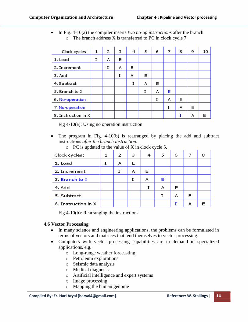
Computer Organization and Architecture Chapter 4 : Pipeline and Vector processing
Compiled By: Er. Hari Aryal [[email protected]] Reference: W. Stallings | 14
In Fig. 4-10(a) the compiler inserts two no-op instructions after the branch.
o The branch address X is transferred to PC in clock cycle 7.
Fig 4-10(a): Using no operation instruction
The program in Fig. 4-10(b) is rearranged by placing the add and subtract
instructions after the branch instruction.
o PC is updated to the value of X in clock cycle 5.
Fig 4-10(b): Rearranging the instructions
4.6 Vector Processing
In many science and engineering applications, the problems can be formulated in
terms of vectors and matrices that lend themselves to vector processing.
Computers with vector processing capabilities are in demand in specialized
applications. e.g.
o Long-range weather forecasting
o Petroleum explorations
o Seismic data analysis
o Medical diagnosis
o Artificial intelligence and expert systems
o Image processing
o Mapping the human genome
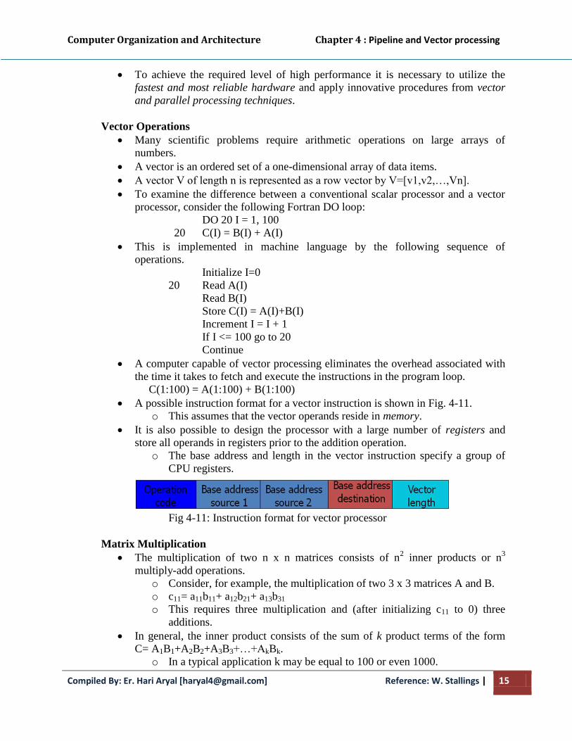
Computer Organization and Architecture Chapter 4 : Pipeline and Vector processing
Compiled By: Er. Hari Aryal [[email protected]] Reference: W. Stallings | 15
To achieve the required level of high performance it is necessary to utilize the
fastest and most reliable hardware and apply innovative procedures from vector
and parallel processing techniques.
Vector Operations
Many scientific problems require arithmetic operations on large arrays of
numbers.
A vector is an ordered set of a one-dimensional array of data items.
A vector V of length n is represented as a row vector by V=[v1,v2,…,Vn].
To examine the difference between a conventional scalar processor and a vector
processor, consider the following Fortran DO loop:
DO 20 I = 1, 100
20 C(I) = B(I) + A(I)
This is implemented in machine language by the following sequence of
operations.
Initialize I=0
20 Read A(I)
Read B(I)
Store C(I) = A(I)+B(I)
Increment I = I + 1
If I <= 100 go to 20
Continue
A computer capable of vector processing eliminates the overhead associated with
the time it takes to fetch and execute the instructions in the program loop.
C(1:100) = A(1:100) + B(1:100)
A possible instruction format for a vector instruction is shown in Fig. 4-11.
o This assumes that the vector operands reside in memory.
It is also possible to design the processor with a large number of registers and
store all operands in registers prior to the addition operation.
o The base address and length in the vector instruction specify a group of
CPU registers.
Fig 4-11: Instruction format for vector processor
Matrix Multiplication
The multiplication of two n x n matrices consists of n2 inner products or n
3
multiply-add operations.
o Consider, for example, the multiplication of two 3 x 3 matrices A and B.
o c11= a11b11+ a12b21+ a13b31
o This requires three multiplication and (after initializing c11 to 0) three
additions.
In general, the inner product consists of the sum of k product terms of the form
C= A1B1+A2B2+A3B3+…+AkBk.
o In a typical application k may be equal to 100 or even 1000.

Computer Organization and Architecture Chapter 4 : Pipeline and Vector processing
Compiled By: Er. Hari Aryal [[email protected]] Reference: W. Stallings | 16
The inner product calculation on a pipeline vector processor is shown in Fig. 4-
12.
161612128844
151511117733
141410106622
1313995511
BABABABA
BABABABA
BABABABA
BABABABAC
Fig 4-12: Pipeline for calculating an inner product
Memory Interleaving
Pipeline and vector processors often require simultaneous access to memory from
two or more sources.
o An instruction pipeline may require the fetching of an instruction and an
operand at the same time from two different segments.
o An arithmetic pipeline usually requires two or more operands to enter the
pipeline at the same time.
Instead of using two memory buses for simultaneous access, the memory can be
partitioned into a number of modules connected to a common memory address
and data buses.
o A memory module is a memory array together with its own address and
data registers.
Fig. 4-13 shows a memory unit with four modules.
Fig 4-13: Multiple module memory organization

Computer Organization and Architecture Chapter 4 : Pipeline and Vector processing
Compiled By: Er. Hari Aryal [[email protected]] Reference: W. Stallings | 17
The advantage of a modular memory is that it allows the use of a technique called
interleaving.
In an interleaved memory, different sets of addresses are assigned to different
memory modules.
By staggering the memory access, the effective memory cycle time can be
reduced by a factor close to the number of modules.
Supercomputers
A commercial computer with vector instructions and pipelined floating-point
arithmetic operations is referred to as a supercomputer.
o To speed up the operation, the components are packed tightly together to
minimize the distance that the electronic signals have to travel.
This is augmented by instructions that process vectors and combinations of
scalars and vectors.
A supercomputer is a computer system best known for its high computational
speed, fast and large memory systems, and the extensive use of parallel
processing.
o It is equipped with multiple functional units and each unit has its own
pipeline configuration.
It is specifically optimized for the type of numerical calculations involving
vectors and matrices of floating-point numbers.
They are limited in their use to a number of scientific applications, such as
numerical weather forecasting, seismic wave analysis, and space research.
A measure used to evaluate computers in their ability to perform a given number
of floating-point operations per second is referred to as flops.
A typical supercomputer has a basic cycle time of 4 to 20 ns.
The examples of supercomputer:
Cray-1: it uses vector processing with 12 distinct functional units in parallel; a
large number of registers (over 150); multiprocessor configuration (Cray X-MP
and Cray Y-MP)
o Fujitsu VP-200: 83 vector instructions and 195 scalar instructions; 300
megaflops
4.7 Array Processing
An array processor is a processor that performs computations on large arrays of
data.
The term is used to refer to two different types of processors.
o Attached array processor:
Is an auxiliary processor.
It is intended to improve the performance of the host computer in
specific numerical computation tasks.
o SIMD array processor:
Has a single-instruction multiple-data organization.
It manipulates vector instructions by means of multiple functional
units responding to a common instruction.
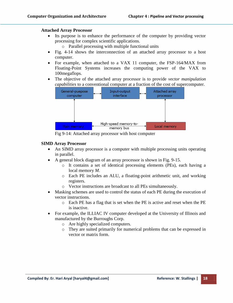
Computer Organization and Architecture Chapter 4 : Pipeline and Vector processing
Compiled By: Er. Hari Aryal [[email protected]] Reference: W. Stallings | 18
Attached Array Processor
Its purpose is to enhance the performance of the computer by providing vector
processing for complex scientific applications.
o Parallel processing with multiple functional units
Fig. 4-14 shows the interconnection of an attached array processor to a host
computer.
For example, when attached to a VAX 11 computer, the FSP-164/MAX from
Floating-Point Systems increases the computing power of the VAX to
100megaflops.
The objective of the attached array processor is to provide vector manipulation
capabilities to a conventional computer at a fraction of the cost of supercomputer.
Fig 9-14: Attached array processor with host computer
SIMD Array Processor
An SIMD array processor is a computer with multiple processing units operating
in parallel.
A general block diagram of an array processor is shown in Fig. 9-15.
o It contains a set of identical processing elements (PEs), each having a
local memory M.
o Each PE includes an ALU, a floating-point arithmetic unit, and working
registers.
o Vector instructions are broadcast to all PEs simultaneously.
Masking schemes are used to control the status of each PE during the execution of
vector instructions.
o Each PE has a flag that is set when the PE is active and reset when the PE
is inactive.
For example, the ILLIAC IV computer developed at the University of Illinois and
manufactured by the Burroughs Corp.
o Are highly specialized computers.
o They are suited primarily for numerical problems that can be expressed in
vector or matrix form.
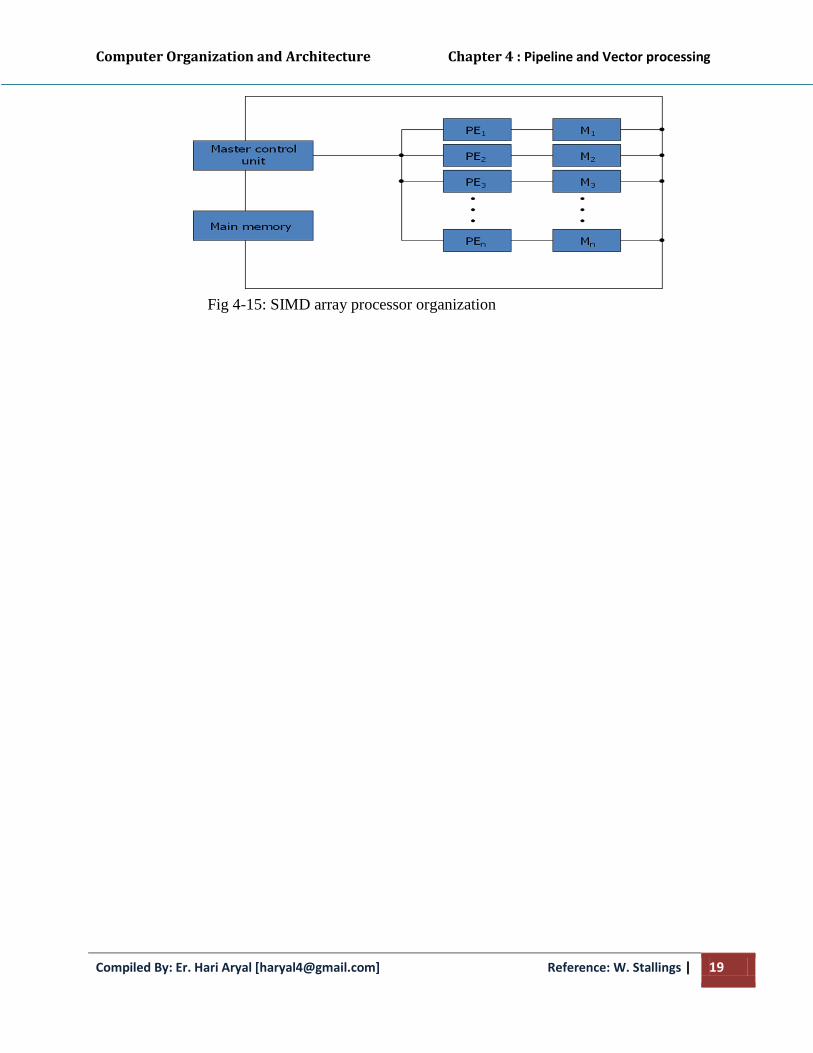
Computer Organization and Architecture Chapter 4 : Pipeline and Vector processing
Compiled By: Er. Hari Aryal [[email protected]] Reference: W. Stallings | 19
Fig 4-15: SIMD array processor organization

Computer Organization and Architecture Chapter 5 : Computer Arithmetic
Compiled By: Er. Hari Aryal [[email protected]] Reference: W. Stallings | 1
Chapter – 5
Computer Arithmetic
Integer Representation: (Fixed-point representation):
An eight bit word can be represented the numbers from zero to 255 including
00000000 = 0
00000001 = 1
- - - - - - -
11111111 = 255
In general if an n-bit sequence of binary digits an-1, an-2 …..a1, a0; is interpreted as unsigned
integer A.
A =
1
0
n
i
2iai
Sign magnitude representation:
There are several alternative convention used to represent negative as well as positive integers,
all of which involves treating the most significant (left most) bit in the word as sign bit. If the
sign bit is 0, the number is +ve and if the sign bit is 1, the number is –ve. In n bit word the right
most n-1 bit hold the magnitude of integer.
For an example,
+18 = 00010010
- 18 = 10010010 (sign magnitude)
The general case can be expressed as follows:
A =
2
0
n
i
2iai if an-1 = 0
= -
2
0
n
i
2iai if an-1 =1
A = -2n-1
an-1 +
2
0
n
i
2iai (Both for +ve and –ve)
There are several drawbacks to sign-magnitude representation. One is that addition or subtraction
requires consideration of both signs of number and their relative magnitude to carry out the
required operation. Another drawback is that there are two representation of zero. For an
example:
+010 = 00000000
-010 = 10000000 this is inconvenient.
2’s complement representation:
Like sign magnitude representation, 2’s complement representation uses the most significant bit
as sign bit making it easy to test whether the integer is negative or positive. It differs from the
use of sign magnitude representation in the way that the other bits are interpreted. For negation,
take the Boolean complement (1’s complement) of each bit of corresponding positive number,
and then add one to the resulting bit pattern viewed as unsigned integer. Consider n bit integer A
in 2’s complement representation. If A is +ve then the sign bit an-1 is zero. The remaining bits
represent the magnitude of the number.

Computer Organization and Architecture Chapter 5 : Computer Arithmetic
Compiled By: Er. Hari Aryal [[email protected]] Reference: W. Stallings | 2
A =
2
0
n
i
2iai for A ≥ 0
The number zero is identified as +ve and therefore has zero sign bit and magnitude of all 0’s. We
can see that the range of +ve integer that may be represented is from 0 (all the magnitude bits
are zero) through 2n-1
-1 (all of the magnitude bits are 1).
Now for –ve number integer A, the sign bit an-1 is 1. The range of –ve integer that can be
represented is from -1 to -2n-1
2’s complement, A = -2n-1
an-1 +
2
0
n
i
2iai
Defines the twos complement of representation of both positive and negative number.
For an example:
+18 = 00010010
1’s complement = 11101101
2’s complement = 11101110 = -18
5.1 Addition Algorithm
5.2 Subtraction Algorithm
1001 = -7 1100 = -4 0011 = 3
0101 = +5 0100 = +4 0100= 4
1110 =-2 10000 = 0 0111= 7 (a) (-7)+(+5) (b) (-4)+(4) (c) (+3)+(+4)
1100 = -4 0101 =5 1001 = -7
1111 = -1 0100 =4 1010 = -6
11011 = -5 1001=overflow 10011 = overflow (d) (-4)+(-1) (e) (+5)+(+4) (f) (-7)+(-6)
The first four examples illustrate successful operation if the result of the operation is +ve then we
get +ve number in ordinary binary notation. If the result of the operation is –ve we get negative
number in twos complement form. Note that in some instants there is carry bit beyond the end of
what which is ignored. On any addition the result may larger then can be held in word size being
use. This condition is called over flow. When overflow occur ALU must signal this fact so that
no attempt is made to use the result. To detect overflow the following rule observed. If two
numbers are added, and they are both +ve or both –ve; then overflow occurs if and only if the
result has the opposite sign.
The data path and hardware elements needed to accomplish addition and subtraction is shown in
figure below. The central element is binary adder, which is presented two numbers for addition
and produces a sum and an overflow indication. The binary adder treats the two numbers as
unsigned integers. For addition, the two numbers are presented to the adder from two registers A
and B. The result may be stored in one of these registers or in the third. The overflow indication
is stored in a 1-bit overflow flag V (where 1 = overflow and 0 = no overflow). For subtraction,
the subtrahend (B register) is passed through a 2’s complement unit so that its 2’s complement is
presented to the adder (a – b = a + (-b)).

Computer Organization and Architecture Chapter 5 : Computer Arithmetic
Compiled By: Er. Hari Aryal [[email protected]] Reference: W. Stallings | 3
B Register A Register
Complement
Switch
n bit Adder
V CSZ
Check for Zero
XORB7
B8
B7
n bit/
Fig: Block diagram of hardware for addition / subtraction
5.3 Multiplication Algorithm
The multiplier and multiplicand bits are loaded into two registers Q and M. A third register A is
initially set to zero. C is the 1-bit register which holds the carry bit resulting from addition. Now,
the control logic reads the bits of the multiplier one at a time. If Q0 is 1, the multiplicand is added
to the register A and is stored back in register A with C bit used for carry. Then all the bits of
CAQ are shifted to the right 1 bit so that C bit goes to An-1, A0 goes to Qn-1 and Q0 is lost. If Q0 is
0, no addition is performed just do the shift. The process is repeated for each bit of the original
multiplier. The resulting 2n bit product is contained in the QA register.
Fig: Block diagram of multiplication

Computer Organization and Architecture Chapter 5 : Computer Arithmetic
Compiled By: Er. Hari Aryal [[email protected]] Reference: W. Stallings | 4
There are three types of operation for multiplication.
It should be determined whether a multiplier bit is 1 or 0 so that it can designate the
partial product. If the multiplier bit is 0, the partial product is zero; if the multiplier bit is
1, the multiplicand is partial product.
It should shift partial product.
It should add partial product.
Unsigned Binary Multiplication
1011 Multiplicand 11
X 1101 Multiplier 13
1011
0000 Partial Product
1011
+ 1011
10001111 Product (143)
Start
M ß Multiplicand, Q ß Multiplier
C, A ß 0, Count ß No. of bits of Q
Is
Q0 = 1
?
A ß A + M
Right Shift C, A, Q
Count ß Count - 1
Is
Count = 0
?
Stop Result in AQ
Yes
Yes
No
No
Fig. : Flowchart of Unsigned Binary Multiplication
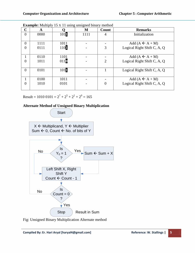
Computer Organization and Architecture Chapter 5 : Computer Arithmetic
Compiled By: Er. Hari Aryal [[email protected]] Reference: W. Stallings | 5
Example: Multiply 15 X 11 using unsigned binary method
C A Q M Count Remarks
0 0000 1011 1111 4 Initialization
0
0
1111
0111
1011
1101
-
-
-
3
Add (A ß A + M)
Logical Right Shift C, A, Q
1
0
0110
1011
1101
0110
-
-
-
2
Add (A ß A + M)
Logical Right Shift C, A, Q
0 0101 1011 - 1 Logical Right Shift C, A, Q
1
0
0100
1010
1011
0101
-
-
-
0
Add (A ß A + M)
Logical Right Shift C, A, Q
Result = 1010 0101 = 27 + 2
5 + 2
2 + 2
0 = 165
Alternate Method of Unsigned Binary Multiplication
Start
X ß Multiplicand, Y ß Multiplier
Sum ß 0, Count ß No. of bits of Y
Is
Y0 = 1
?
Sum ß Sum + X
Left Shift X, Right
Shift Y
Count ß Count - 1
Is
Count = 0
?
Stop Result in Sum
Yes
Yes
No
No
Fig: Unsigned Binary Multiplication Alternate method

Computer Organization and Architecture Chapter 5 : Computer Arithmetic
Compiled By: Er. Hari Aryal [[email protected]] Reference: W. Stallings | 6
Algorithm:
Step 1: Clear the sum (accumulator A). Place the multiplicand in X and multiplier in Y.
Step 2: Test Y0; if it is 1, add content of X to the accumulator A.
Step 3: Logical Shift the content of X left one position and content of Y right one position.
Step 4: Check for completion; if not completed, go to step 2.
Example: Multiply 7 X 6
Sum X Y Count Remarks
000000 000111 110 3
Initialization
000000 001110 011 2
Left shift X, Right Shift Y
001110 011100 001 1
Sum ß Sum + X,
Left shift X, Right Shift Y
101010 111000 000 0
Sum ß Sum + X,
Left shift X, Right Shift Y
Result = 101010 = 25 + 2
3 + 2
1 = 42
Signed Multiplication (Booth Algorithm) – 2’s Complement Multiplication
Multiplier and multiplicand are placed in Q and M register respectively. There is also one bit
register placed logically to the right of the least significant bit Q0 of the Q register and designated
as Q-1. The result of multiplication will appear in A and Q resister. A and Q-1 are initialized to
zero if two bits (Q0 and Q-1) are the same (11 or 00) then all the bits of A, Q and Q-1 registers are
shifted to the right 1 bit. If the two bits differ then the multiplicand is added to or subtracted from
the A register depending on weather the two bits are 01 or 10. Following the addition or
subtraction the arithmetic right shift occurs. When count reaches to zero, result resides into AQ
in the form of signed integer [-2n-1
*an-1 + 2n-2
*an-2 + …………… + 21*a1 + 2
0*a0].

Computer Organization and Architecture Chapter 5 : Computer Arithmetic
Compiled By: Er. Hari Aryal [[email protected]] Reference: W. Stallings | 7
Start
Initialize A ß 0, Q-1 ß 0,
M ß Multiplicand, Q ß Multiplier,
Count ß No. of bits of Q
Is
Q0Q-1
?
A ß A + M
Arithmetic Shift Right
A, Q, Q-1
Count ß Count - 1
Is
Count = 0
?
Stop Result in AQ
Yes
= 01
No
= 10
= 11
= 00
A ß A - M
Fig.: Flowchart of Signed Binary Numbers (using 2’s Complement, Booth Method)
Example: Multiply 9 X -3 = -27 using Booth Algorithm
+3 = 00011, -3 = 11101 (2’s complement of +3)
A Q Q-1 Add (M) Sub ( M +1) Count Remarks
00000 11101 0 01001 10111 5 Initialization
10111
11011
11101
11110
0
1
-
-
-
-
-
4
Sub (A ß A - M) as Q0Q-1 = 10
Arithmetic Shift Right A, Q, Q-1
00100
00010
11110
01111
1
0
-
-
-
-
-
3
Add (A ß A + M) as Q0Q-1 = 01
Arithmetic Shift Right A, Q, Q-1
11001
11100
01111
10111
0
1
-
-
-
-
-
2
Sub (A ß A - M) as Q0Q-1 = 10
Arithmetic Shift Right A, Q, Q-1
11110 01011 1 - - 1 Arithmetic Shift Right A, Q, Q-1
as Q0Q-1 = 11
11111 00101 1 - - 0 Arithmetic Shift Right A, Q, Q-1
as Q0Q-1 = 11
Result in AQ = 11111 00101 = -29+2
8+2
7+2
6+2
5+2
2+2
0 = -512+256+128+64+32+4+1 = -27
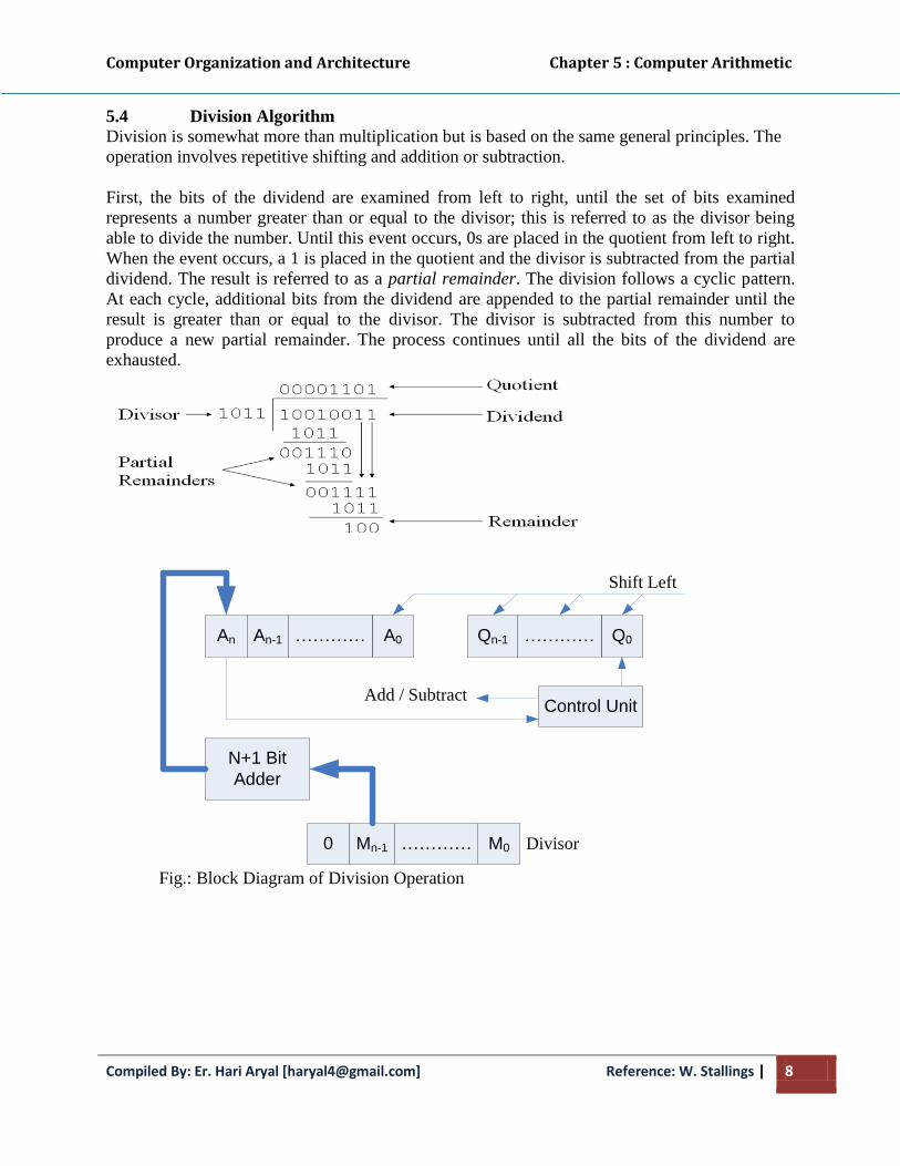
Computer Organization and Architecture Chapter 5 : Computer Arithmetic
Compiled By: Er. Hari Aryal [[email protected]] Reference: W. Stallings | 8
5.4 Division Algorithm
Division is somewhat more than multiplication but is based on the same general principles. The
operation involves repetitive shifting and addition or subtraction.
First, the bits of the dividend are examined from left to right, until the set of bits examined
represents a number greater than or equal to the divisor; this is referred to as the divisor being
able to divide the number. Until this event occurs, 0s are placed in the quotient from left to right.
When the event occurs, a 1 is placed in the quotient and the divisor is subtracted from the partial
dividend. The result is referred to as a partial remainder. The division follows a cyclic pattern.
At each cycle, additional bits from the dividend are appended to the partial remainder until the
result is greater than or equal to the divisor. The divisor is subtracted from this number to
produce a new partial remainder. The process continues until all the bits of the dividend are
exhausted.
An A0…………An-1 Q0…………Qn-1
N+1 Bit
Adder
0 M0…………Mn-1
Shift Left
Control UnitAdd / Subtract
Divisor
Fig.: Block Diagram of Division Operation

Computer Organization and Architecture Chapter 5 : Computer Arithmetic
Compiled By: Er. Hari Aryal [[email protected]] Reference: W. Stallings | 9
Restoring Division (Unsigned Binary Division)
Algorithm:
Step 1: Initialize A, Q and M registers to zero, dividend and divisor respectively and counter to n
where n is the number of bits in the dividend.
Step 2: Shift A, Q left one binary position.
Step 3: Subtract M from A placing answer back in A. If sign of A is 1, set Q0 to zero and add M
back to A (restore A). If sign of A is 0, set Q0 to 1.
Step 4: Decrease counter; if counter > 0, repeat process from step 2 else stop the process. The
final remainder will be in A and quotient will be in Q.

Computer Organization and Architecture Chapter 5 : Computer Arithmetic
Compiled By: Er. Hari Aryal [[email protected]] Reference: W. Stallings | 10
Example: Divide 15 (1111) by 4 (0100)
A Q M M +1 Count Remarks
00000 1111 00100 11100 4 Initialization
00001
11101
00001
111□ 111□
1110
-
-
-
-
-
-
-
-
3
Shift Left A, Q
Sub (A ß A – M)
Q0 ß 0, Add (Aß A + M)
00011
11111
00011
110□
110□
1100
-
-
-
-
-
-
-
-
2
Shift Left A, Q
Sub (A ß A – M)
Q0 ß 0, Add (Aß A + M)
00111
00011
00011
100□
100□
1001
-
-
-
-
-
-
-
-
1
Shift Left A, Q
Sub (A ß A – M)
Set Q0 ß 1
00111
00011
00011
001□
001□
0011
-
-
-
-
-
-
-
-
0
Shift Left A, Q
Sub (A ß A – M)
Set Q0 ß 1
Quotient in Q = 0011 = 3
Remainder in A = 00011 = 3
Non – Restoring Division (Signed Binary Division)
Algorithm
Step 1: Initialize A, Q and M registers to zero, dividend and divisor respectively and count to
number of bits in dividend.
Step 2: Check sign of A;
If A < 0 i.e. bn-1 is 1
a. Shift A, Q left one binary position.
b. Add content of M to A and store back in A.
If A ≥ 0 i.e. bn-1 is 0
a. Shift A, Q left one binary position.
b. Subtract content of M to A and store back in A.
Step 3: If sign of A is 0, set Q0 to 1 else set Q0 to 0.
Step 4: Decrease counter. If counter > 0, repeat process from step 2 else go to step 5.
Step 5: If A ≥ 0 i.e. positive, content of A is remainder else add content of M to A to get the
remainder. The quotient will be in Q.

Computer Organization and Architecture Chapter 5 : Computer Arithmetic
Compiled By: Er. Hari Aryal [[email protected]] Reference: W. Stallings | 11
Start
Initialize: A ß 0, M ß Divisor,
Q ß Dividend, Count ß No. of bits of Q
Is
A < 0
?
Left Shift AQ
Count ß Count - 1
Is
Count > 0
?
Stop
Quotient in Q
Remainder in A
Yes
Yes
Yes
NoLeft Shift AQ
A ß A + M A ß A - M
Is
A < 0
?
Q0 ß 0Q0 ß 1YesNo
Is
A > 0
?
A ß A + MNo
No

Computer Organization and Architecture Chapter 5 : Computer Arithmetic
Compiled By: Er. Hari Aryal [[email protected]] Reference: W. Stallings | 12
Example: Divide 1110 (14) by 0011 (3) using non-restoring division.
A Q M M +1 Count Remarks
00000 1110 00011 11101 4 Initialization
00001
11110
11110
110□ 110□
1100
-
-
-
-
-
-
-
-
3
Shift Left A, Q
Sub (A ß A – M)
Set Q0 to 0
11101
00000
00000
100□
100□
1001
-
-
-
-
-
-
-
-
2
Shift Left A, Q
Add (A ß A + M)
Set Q0 to 1
00001
11110
11110
001□
001□
0010
-
-
-
-
-
-
-
-
1
Shift Left A, Q
Sub (A ß A – M)
Set Q0 to 0
11100
11111
11111
010□
010□
0100
-
-
-
-
-
-
-
-
0
Shift Left A, Q
Add (A ß A + M)
Set Q0 to 0
00010 0100 - - - Add (A ß A + M)
Quotient in Q = 0011 = 3
Remainder in A = 00010 = 2

Computer Organization and Architecture Chapter 5 : Computer Arithmetic
Compiled By: Er. Hari Aryal [[email protected]] Reference: W. Stallings | 13
Floating Point Representation
The floating point representation of the number has two parts. The first part represents a signed
fixed point numbers called mantissa or significand. The second part designates the position of
the decimal (or binary) point and is called exponent. For example, the decimal no + 6132.789 is
represented in floating point with fraction and exponent as follows.
Fraction Exponent
+0.6132789 +04
This representation is equivalent to the scientific notation +0.6132789 × 10+4
The floating point is always interpreted to represent a number in the following form ±M × R±E
.
Only the mantissa M and the exponent E are physically represented in the register (including
their sign). The radix R and the radix point position of the mantissa are always assumed.
A floating point binary no is represented in similar manner except that it uses base 2 for the
exponent.
For example, the binary no +1001.11 is represented with 8 bit fraction and 0 bit exponent as
follows.
0.1001110 × 2100
Fraction Exponent
01001110 000100
The fraction has zero in the leftmost position to denote positive. The floating point number is
equivalent to M × 2E = +(0.1001110)2 × 2
+4
Floating Point Arithmetic
The basic operations for floating point arithmetic are
Floating point number Arithmetic Operations
X = Xs × BXE
X + Y = (Xs × BXE-YE
+ Ys) × BYE
Y = Ys × BYE
X - Y = (Xs × BXE-YE
- Ys) × BYE
X * Y = (Xs × Ys) × BXE+YE
X / Y = (Xs / Ys) × BXE-YE
There are four basic operations for floating point arithmetic. For addition and subtraction, it is
necessary to ensure that both operands have the same exponent values. This may require shifting
the radix point on one of the operands to achieve alignment. Multiplication and division are
straighter forward.
A floating point operation may produce one of these conditions:
Exponent Overflow: A positive exponent exceeds the maximum possible exponent value.
Exponent Underflow: A negative exponent which is less than the minimum possible
value.
Significand Overflow: The addition of two significands of the same sign may carry in a
carry out of the most significant bit.
Significand underflow: In the process of aligning significands, digits may flow off the
right end of the significand.

Computer Organization and Architecture Chapter 5 : Computer Arithmetic
Compiled By: Er. Hari Aryal [[email protected]] Reference: W. Stallings | 14
Floating Point Addition and Subtraction
In floating point arithmetic, addition and subtraction are more complex than multiplication and
division. This is because of the need for alignment. There are four phases for the algorithm for
floating point addition and subtraction.
1. Check for zeros:
Because addition and subtraction are identical except for a sign change, the process
begins by changing the sign of the subtrahend if it is a subtraction operation. Next; if one
is zero, second is result.
2. Align the Significands:
Alignment may be achieved by shifting either the smaller number to the right (increasing
exponent) or shifting the large number to the left (decreasing exponent).
3. Addition or subtraction of the significands:
The aligned significands are then operated as required.
4. Normalization of the result:
Normalization consists of shifting significand digits left until the most significant bit is
nonzero.
Example: Addition
X = 0.10001 * 2110
Y = 0.101 * 2100
Since EY < EX, Adjust Y
Y = 0.00101 * 2100
* 2010
= 0.00101 * 2110
So, EZ = EX = EY = 110
Now, MZ = MX + MY = 0.10001 + 0.00101 = 0.10110
Hence, Z = MZ * 2EZ
= 0.10110 * 2110
Example: Subtraction
X = 0.10001 * 2110
Y = 0.101 * 2100
Since EY < EX, Adjust Y
Y = 0.00101 * 2100
* 2010
= 0.00101 * 2110
So, EZ = EX = EY = 110
Now, MZ = MX - MY = 0.10001 - 0.00101 = 0.01100
Z = MZ * 2EZ
= 0.01100 * 2110
(Un-Normalized)
Hence, Z = 0.1100 * 2110
* 2-001
= 0.1100 * 2101
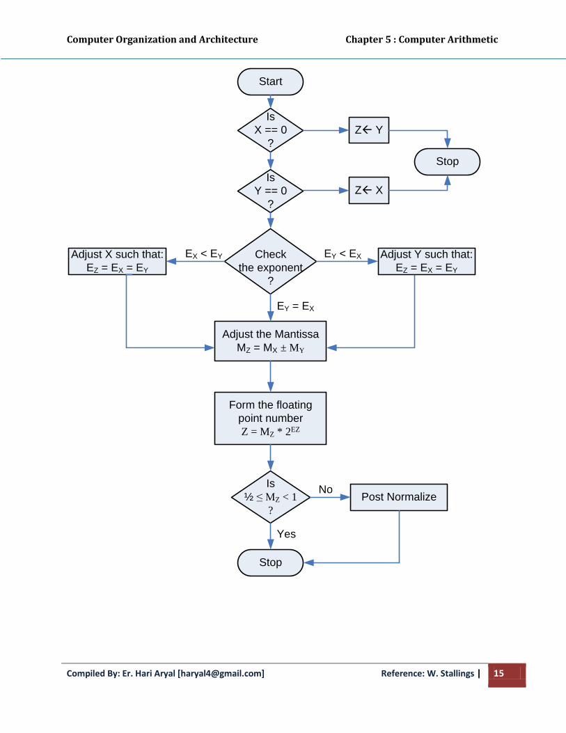
Computer Organization and Architecture Chapter 5 : Computer Arithmetic
Compiled By: Er. Hari Aryal [[email protected]] Reference: W. Stallings | 15
Start
Check
the exponent
?
Adjust the Mantissa
MZ = MX ± MY
Is
½ ≤ MZ < 1
?
Stop
Yes
No
Adjust X such that:
EZ = EX = EY
Is
X == 0
?
Zß Y
Is
Y == 0
?
Zß X
Stop
Adjust Y such that:
EZ = EX = EY
EY < EXEX < EY
EY = EX
Form the floating
point number
Z = MZ * 2EZ
Post Normalize

Computer Organization and Architecture Chapter 5 : Computer Arithmetic
Compiled By: Er. Hari Aryal [[email protected]] Reference: W. Stallings | 16
Floating Point Multiplication
The multiplication can be subdivided into 4 parts.
1. Check for zeroes.
2. Add the exponents.
3. Multiply mantissa.
4. Normalize the product.
Example: X = 0.101 * 2
110 0.1001
Y = 0.1001 * 2-010
* 0.101
As we know, Z = X * Y = (MX * MY) * 2(EX + EY)
1001
Z = (0.101 * 0.1001) * 2(110-010)
0000*
= 0.0101101 * 2100
+1001**
= 0.101101 * 2011
(Normalized) 101101 = 0.0101101

Computer Organization and Architecture Chapter 5 : Computer Arithmetic
Compiled By: Er. Hari Aryal [[email protected]] Reference: W. Stallings | 17
Floating Point Division
The division algorithm can be subdivided into 5 parts
1. Check for zeroes.
2. Initial registers and evaluates the sign.
3. Align the dividend.
4. Subtract the exponent.
5. Divide the mantissa.
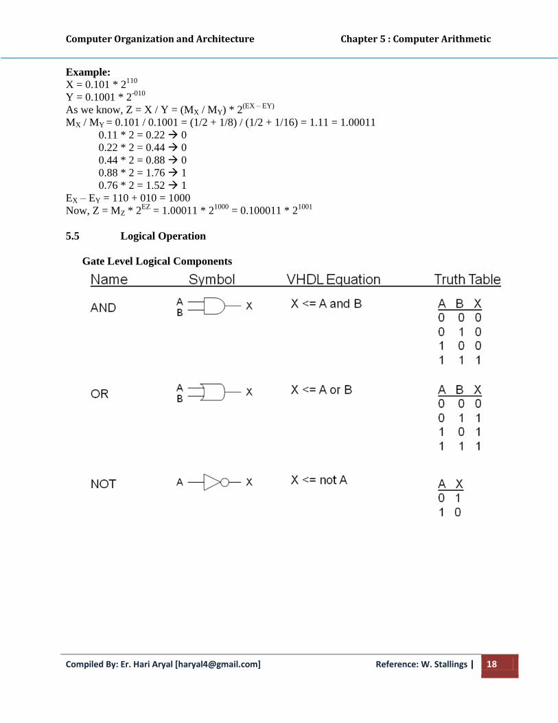
Computer Organization and Architecture Chapter 5 : Computer Arithmetic
Compiled By: Er. Hari Aryal [[email protected]] Reference: W. Stallings | 18
Example:
X = 0.101 * 2110
Y = 0.1001 * 2-010
As we know, Z = X / Y = (MX / MY) * 2(EX – EY)
MX / MY = 0.101 / 0.1001 = (1/2 + 1/8) / (1/2 + 1/16) = 1.11 = 1.00011
0.11 * 2 = 0.22 0
0.22 * 2 = 0.44 0
0.44 * 2 = 0.88 0
0.88 * 2 = 1.76 1
0.76 * 2 = 1.52 1
EX – EY = 110 + 010 = 1000
Now, Z = MZ * 2EZ
= 1.00011 * 21000
= 0.100011 * 21001
5.5 Logical Operation
Gate Level Logical Components
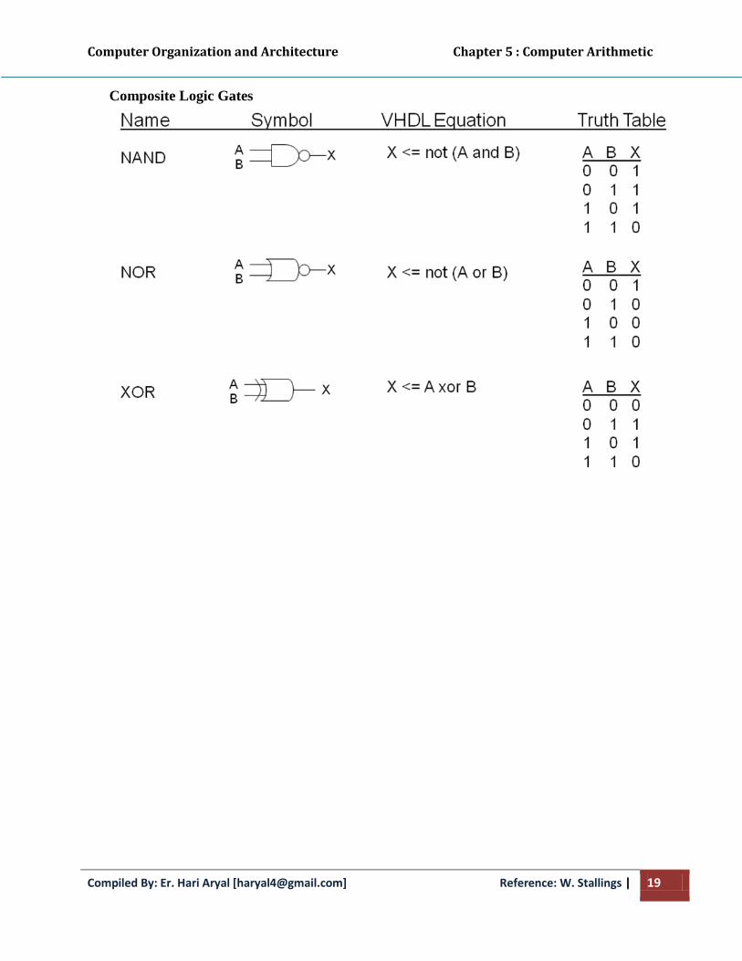
Computer Organization and Architecture Chapter 5 : Computer Arithmetic
Compiled By: Er. Hari Aryal [[email protected]] Reference: W. Stallings | 19
Composite Logic Gates

Computer Organization and Architecture Chapter 6 : Memory System
Compiled By: Er. Hari Aryal [[email protected]] Reference: W. Stallings & M. Mano | 1
Chapter – 6
Memory System
6.1 Microcomputer Memory
Memory is an essential component of the microcomputer system.
It stores binary instructions and datum for the microcomputer.
The memory is the place where the computer holds current programs and data that are in
use.
None technology is optimal in satisfying the memory requirements for a computer
system.
Computer memory exhibits perhaps the widest range of type, technology, organization,
performance and cost of any feature of a computer system.
The memory unit that communicates directly with the CPU is called main memory.
Devices that provide backup storage are called auxiliary memory or secondary memory.
6.2 Characteristics of memory systems
The memory system can be characterised with their Location, Capacity, Unit of transfer,
Access method, Performance, Physical type, Physical characteristics, Organisation.
Location
• Processor memory: The memory like registers is included within the processor and
termed as processor memory.
• Internal memory: It is often termed as main memory and resides within the CPU.
• External memory: It consists of peripheral storage devices such as disk and magnetic
tape that are accessible to processor via i/o controllers.
Capacity
• Word size: Capacity is expressed in terms of words or bytes.
— The natural unit of organisation
• Number of words: Common word lengths are 8, 16, 32 bits etc.
— or Bytes
Unit of Transfer
• Internal: For internal memory, the unit of transfer is equal to the number of data lines
into and out of the memory module.
• External: For external memory, they are transferred in block which is larger than a
word.
• Addressable unit
— Smallest location which can be uniquely addressed
— Word internally
— Cluster on Magnetic disks
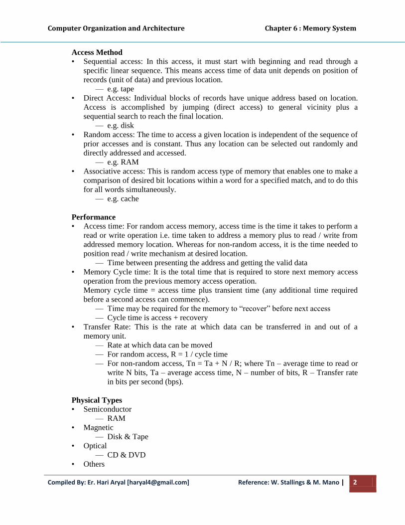
Computer Organization and Architecture Chapter 6 : Memory System
Compiled By: Er. Hari Aryal [[email protected]] Reference: W. Stallings & M. Mano | 2
Access Method
• Sequential access: In this access, it must start with beginning and read through a
specific linear sequence. This means access time of data unit depends on position of
records (unit of data) and previous location.
— e.g. tape
• Direct Access: Individual blocks of records have unique address based on location.
Access is accomplished by jumping (direct access) to general vicinity plus a
sequential search to reach the final location.
— e.g. disk
• Random access: The time to access a given location is independent of the sequence of
prior accesses and is constant. Thus any location can be selected out randomly and
directly addressed and accessed.
— e.g. RAM
• Associative access: This is random access type of memory that enables one to make a
comparison of desired bit locations within a word for a specified match, and to do this
for all words simultaneously.
— e.g. cache
Performance
• Access time: For random access memory, access time is the time it takes to perform a
read or write operation i.e. time taken to address a memory plus to read / write from
addressed memory location. Whereas for non-random access, it is the time needed to
position read / write mechanism at desired location.
— Time between presenting the address and getting the valid data
• Memory Cycle time: It is the total time that is required to store next memory access
operation from the previous memory access operation.
Memory cycle time = access time plus transient time (any additional time required
before a second access can commence).
— Time may be required for the memory to “recover” before next access
— Cycle time is access + recovery
• Transfer Rate: This is the rate at which data can be transferred in and out of a
memory unit.
— Rate at which data can be moved
— For random access, R = 1 / cycle time
— For non-random access, Tn = Ta + N / R; where Tn – average time to read or
write N bits, Ta – average access time, N – number of bits, R – Transfer rate
in bits per second (bps).
Physical Types
• Semiconductor
— RAM
• Magnetic
— Disk & Tape
• Optical
— CD & DVD
• Others
Computer Organization and Architecture Chapter 6 : Memory System
Compiled By: Er. Hari Aryal [[email protected]] Reference: W. Stallings & M. Mano | 3
— Bubble
— Hologram
Physical Characteristics
• Decay: Information decays mean data loss.
• Volatility: Information decays when electrical power is switched off.
• Erasable: Erasable means permission to erase.
• Power consumption: how much power consumes?
Organization
• Physical arrangement of bits into words
• Not always obvious
- e.g. interleaved
6.3 The Memory Hierarchy
Capacity, cost and speed of different types of memory play a vital role while designing a
memory system for computers.
If the memory has larger capacity, more application will get space to run smoothly.
It's better to have fastest memory as far as possible to achieve a greater performance.
Moreover for the practical system, the cost should be reasonable.
There is a tradeoff between these three characteristics cost, capacity and access time. One
cannot achieve all these quantities in same memory module because
If capacity increases, access time increases (slower) and due to which cost per bit
decreases.
If access time decreases (faster), capacity decreases and due to which cost per bit
increases.
The designer tries to increase capacity because cost per bit decreases and the more
application program can be accommodated. But at the same time, access time increases
and hence decreases the performance.
So the best idea will be to use memory hierarchy.
Memory Hierarchy is to obtain the highest possible access speed while minimizing the
total cost of the memory system.
Not all accumulated information is needed by the CPU at the same time.
Therefore, it is more economical to use low-cost storage devices to serve as a backup for
storing the information that is not currently used by CPU
The memory unit that directly communicate with CPU is called the main memory
Devices that provide backup storage are called auxiliary memory
The memory hierarchy system consists of all storage devices employed in a computer
system from the slow by high-capacity auxiliary memory to a relatively faster main
memory, to an even smaller and faster cache memory
The main memory occupies a central position by being able to communicate directly with
the CPU and with auxiliary memory devices through an I/O processor
A special very-high-speed memory called cache is used to increase the speed of
processing by making current programs and data available to the CPU at a rapid rate
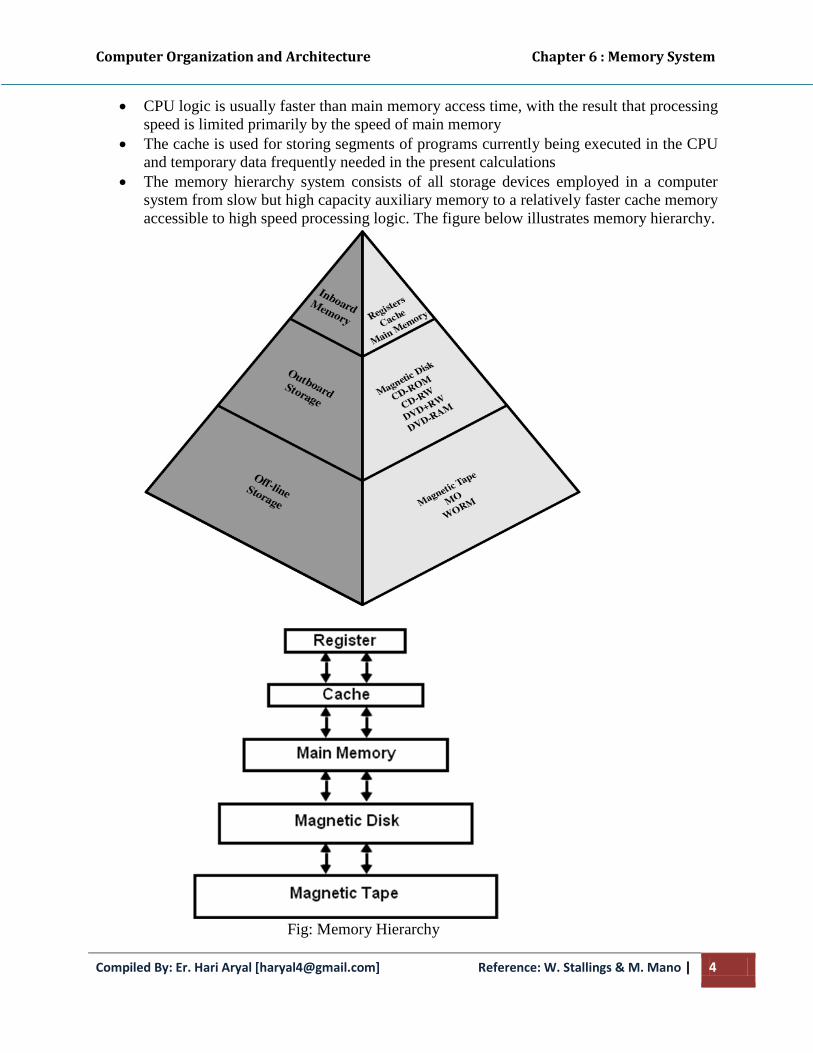
Computer Organization and Architecture Chapter 6 : Memory System
Compiled By: Er. Hari Aryal [[email protected]] Reference: W. Stallings & M. Mano | 4
CPU logic is usually faster than main memory access time, with the result that processing
speed is limited primarily by the speed of main memory
The cache is used for storing segments of programs currently being executed in the CPU
and temporary data frequently needed in the present calculations
The memory hierarchy system consists of all storage devices employed in a computer
system from slow but high capacity auxiliary memory to a relatively faster cache memory
accessible to high speed processing logic. The figure below illustrates memory hierarchy.
Fig: Memory Hierarchy
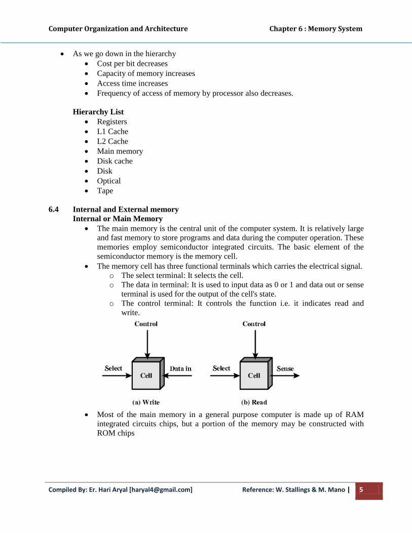
Computer Organization and Architecture Chapter 6 : Memory System
Compiled By: Er. Hari Aryal [[email protected]] Reference: W. Stallings & M. Mano | 5
As we go down in the hierarchy
Cost per bit decreases
Capacity of memory increases
Access time increases
Frequency of access of memory by processor also decreases.
Hierarchy List
Registers
L1 Cache
L2 Cache
Main memory
Disk cache
Disk
Optical
Tape
6.4 Internal and External memory
Internal or Main Memory
The main memory is the central unit of the computer system. It is relatively large
and fast memory to store programs and data during the computer operation. These
memories employ semiconductor integrated circuits. The basic element of the
semiconductor memory is the memory cell.
The memory cell has three functional terminals which carries the electrical signal.
o The select terminal: It selects the cell.
o The data in terminal: It is used to input data as 0 or 1 and data out or sense
terminal is used for the output of the cell's state.
o The control terminal: It controls the function i.e. it indicates read and
write.
Most of the main memory in a general purpose computer is made up of RAM
integrated circuits chips, but a portion of the memory may be constructed with
ROM chips

Computer Organization and Architecture Chapter 6 : Memory System
Compiled By: Er. Hari Aryal [[email protected]] Reference: W. Stallings & M. Mano | 6
RAM– Random Access memory
Memory cells can be accessed for information transfer from any desired random
location.
The process of locating a word in memory is the same and requires of locating a
word in memory is the same and requires an equal amount of time no matter
where the cells are located physically in memory thus named 'Random access'.
Integrated RAM are available in two possible operating modes, Static and
Dynamic
Static RAM (SRAM)
The static RAM consists of flip flop that stores binary information and this stored
information remains valid as long as power is applied to the unit.
Fig: SRAM structure
Four transistors T1, T2, T3 and t4 are cross connected in an arrangement that
produces a stable logical state.
In logic state 1, point C1 is high and point C2 is low. In this state, T1 & T4 are off
and T2 & T3 are on.
In logic state 0, point C1 is low and C2 is high. In this state, T1 & T4 are on and
T2 & T3 are off.
The address line controls the two transistors T5 & T6. When a signal is applied to
this line, the two transistors are switched on allowing for read and write operation.
For a write operation, the desired bit value is applied to line B while it's
complement is applied to line B complement. This forces the four transistors T1,
T2, T3 & T4 into a proper state.
For the read operation, the bit value is read from line B.
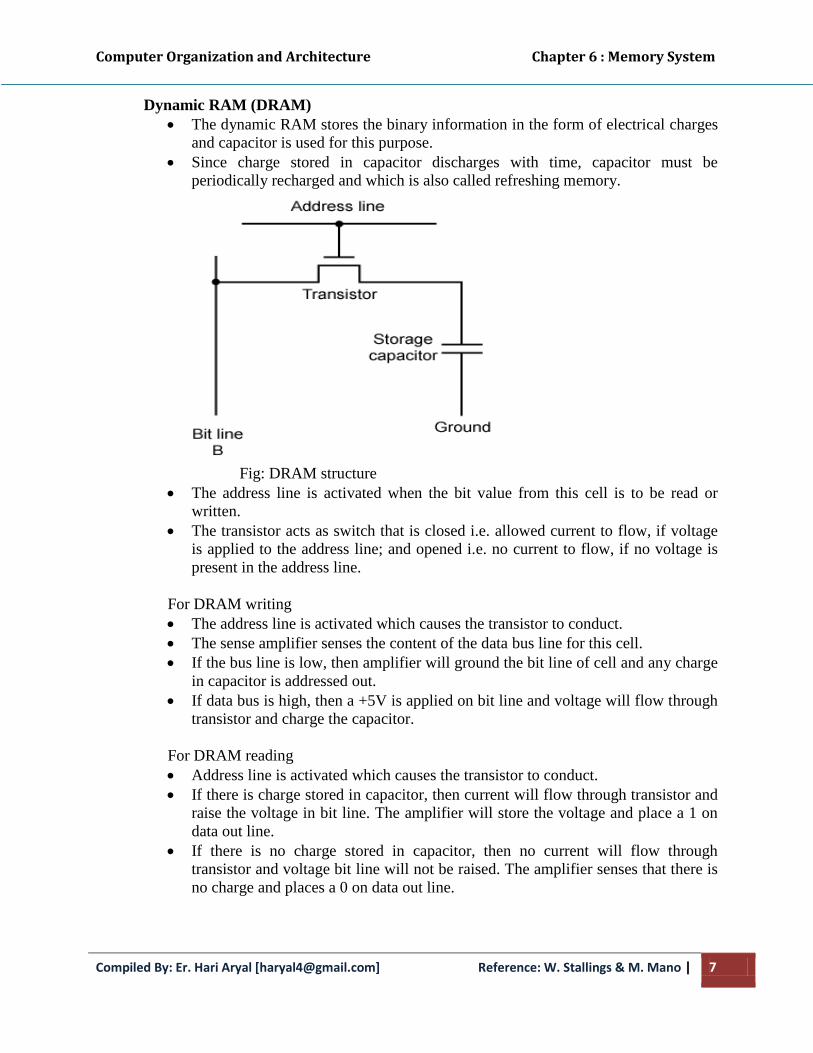
Computer Organization and Architecture Chapter 6 : Memory System
Compiled By: Er. Hari Aryal [[email protected]] Reference: W. Stallings & M. Mano | 7
Dynamic RAM (DRAM)
The dynamic RAM stores the binary information in the form of electrical charges
and capacitor is used for this purpose.
Since charge stored in capacitor discharges with time, capacitor must be
periodically recharged and which is also called refreshing memory.
Fig: DRAM structure
The address line is activated when the bit value from this cell is to be read or
written.
The transistor acts as switch that is closed i.e. allowed current to flow, if voltage
is applied to the address line; and opened i.e. no current to flow, if no voltage is
present in the address line.
For DRAM writing
The address line is activated which causes the transistor to conduct.
The sense amplifier senses the content of the data bus line for this cell.
If the bus line is low, then amplifier will ground the bit line of cell and any charge
in capacitor is addressed out.
If data bus is high, then a +5V is applied on bit line and voltage will flow through
transistor and charge the capacitor.
For DRAM reading
Address line is activated which causes the transistor to conduct.
If there is charge stored in capacitor, then current will flow through transistor and
raise the voltage in bit line. The amplifier will store the voltage and place a 1 on
data out line.
If there is no charge stored in capacitor, then no current will flow through
transistor and voltage bit line will not be raised. The amplifier senses that there is
no charge and places a 0 on data out line.

Computer Organization and Architecture Chapter 6 : Memory System
Compiled By: Er. Hari Aryal [[email protected]] Reference: W. Stallings & M. Mano | 8
SRAM versus DRAM
Both volatile
o Power needed to preserve data
Static RAM
o Uses flip flop to store information
o Needs more space
o Faster, digital device
o Expensive, big in size
o Don't require refreshing circuit
o Used in cache memory
Dynamic RAM
o Uses capacitor to store information
o More dense i.e. more cells can be accommodated per unit area
o Slower, analog device
o Less expensive, small in size
o Needs refreshing circuit
o Used in main memory, larger memory units
ROM– Read Only memory
Read only memory (ROM) contains a permanent pattern of data that cannot be
changed.
A ROM is non-volatile that is no power source is required to maintain the bit
values in memory.
While it is possible to read a ROM, it is not possible to write new data into it.
The data or program is permanently presented in main memory and never be
loaded from a secondary storage device with the advantage of ROM.
A ROM is created like any other integrated circuit chip, with the data actually
wired into the chip as part of the fabrication process.
It presents two problems
o The data insertion step includes a relatively large fixed cost, whether one
or thousands of copies of a particular ROM are fabricated.
o There is no room for error. If one bit is wrong, the whole batch of ROM
must be thrown out.
Types of ROM
Programmable ROM (PROM)
o It is non-volatile and may be written into only once. The writing process is
performed electrically and may be performed by a supplier or customer at
a time later than the original chip fabrication.
Erasable Programmable ROM (EPROM)
o It is read and written electrically. However, before a write operation, all
the storage cells must be erased to the same initial state by exposure of the
packaged chip to ultraviolet radiation (UV ray). Erasure is performed by
shining an intense ultraviolet light through a window that is designed into
the memory chip. EPROM is optically managed and more expensive than
PROM, but it has the advantage of the multiple update capability.
Computer Organization and Architecture Chapter 6 : Memory System
Compiled By: Er. Hari Aryal [[email protected]] Reference: W. Stallings & M. Mano | 9
Electrically Erasable programmable ROM (EEPROM)
o This is a read mostly memory that can be written into at any time without
erasing prior contents, only the byte or byte addresses are updated. The
write operation takes considerably longer than the read operation, on the
order of several hundred microseconds per byte. The EEPROM combines
the advantage of non-volatility with the flexibility of being updatable in
place, using ordinary bus control, addresses and data lines. EEPROM is
more expensive than EPROM and also is less dense, supporting fewer bits
per chip.
Flash Memory
o Flash memory is also the semiconductor memory and because of the speed
with which it can be reprogrammed, it is termed as flash. It is interpreted
between EPROM and EEPROM in both cost and functionality. Like
EEPROM, flash memory uses an electrical erasing technology. An entire
flash memory can be erased in one or a few seconds, which is much faster
than EPROM. In addition, it is possible to erase just blocks of memory
rather than an entire chip. However, flash memory doesn't provide byte
level erasure, a section of memory cells are erased in an action or 'flash'.
External Memory
The devices that provide backup storage are called external memory or auxiliary
memory. It includes serial access type such as magnetic tapes and random access
type such as magnetic disks.
Magnetic Tape
A magnetic tape is the strip of plastic coated with a magnetic recording medium.
Data can be recorded and read as a sequence of character through read / write
head. It can be stopped, started to move forward or in reverse or can be rewound.
Data on tapes are structured as number of parallel tracks running length wise.
Earlier tape system typically used nine tracks. This made it possible to store data
one byte at a time with additional parity bit as 9th track. The recording of data in
this form is referred to as parallel recording.
Magnetic Disk
A magnetic disk is a circular plate constructed with metal or plastic coated with
magnetic material often both side of disk are used and several disk stacked on one
spindle which Read/write head available on each surface. All disks rotate together
at high speed. Bits are stored in magnetize surface in spots along concentric
circles called tracks. The tracks are commonly divided into sections called
sectors. After the read/write head are positioned in specified track the system has
to wait until the rotating disk reaches the specified sector under read/write head.
Information transfer is very fast once the beginning of sector has been reached.
Disk that are permanently attached to the unit assembly and cannot be used by
occasional user are called hard disk drive with removal disk is called floppy disk.
Computer Organization and Architecture Chapter 6 : Memory System
Compiled By: Er. Hari Aryal [[email protected]] Reference: W. Stallings & M. Mano | 10
Optical Disk
The huge commercial success of CD enabled the development of low cost optical
disk storage technology that has revolutionized computer data storage. The disk is
form from resin such as polycarbonate. Digitally recorded information is
imprinted as series of microscopic pits on the surface of poly carbonate. This is
done with the finely focused high intensity leaser. The pitted surface is then
coated with reflecting surface usually aluminum or gold. The shiny surface is
protected against dust and scratches by the top coat of acrylic.
Information is retrieved from CD by low power laser. The intensity of reflected
light of laser changes as it encounters a pit. Specifically if the laser beam falls on
pit which has somewhat rough surface the light scatters and low intensity is
reflected back to the surface. The areas between pits are called lands. A land is a
smooth surface which reflects back at higher intensity. The change between pits
and land is detected by photo sensor and converted into digital signal. The sensor
tests the surface at regular interval.
DVD-Technology
Multi-layer
Very high capacity (4.7G per layer)
Full length movie on single disk
Using MPEG compression
Finally standardized (honest!)
Movies carry regional coding
Players only play correct region films
DVD-Writable
Loads of trouble with standards
First generation DVD drives may not read first generation DVD-W disks
First generation DVD drives may not read CD-RW disks
6.5 Cache memory principles
Principles
o Intended to give memory speed approaching that of fastest memories available but with
large size, at close to price of slower memories
o Cache is checked first for all memory references.
o If not found, the entire block in which that reference resides in main memory is stored in
a cache slot, called a line
o Each line includes a tag (usually a portion of the main memory address) which identifies
which particular block is being stored
o Locality of reference implies that future references will likely come from this block of
memory, so that cache line will probably be utilized repeatedly.
o The proportion of memory references, which are found already stored in cache, is called
the hit ratio.

Computer Organization and Architecture Chapter 6 : Memory System
Compiled By: Er. Hari Aryal [[email protected]] Reference: W. Stallings & M. Mano | 11
Cache memory is intended to give memory speed approaching that of the fastest
memories available, and at the same time provide a large memory size at the price of less
expensive types of semiconductor memories. There is a relatively large and slow main
memory together with a smaller, faster cache memory contains a copy of portions of
main memory.
When the processor attempts to read a word of memory, a check is made to determine if
the word is in the cache. If so, the word is delivered to the processor. If not, a block of
main memory, consisting of fixed number of words is read into the cache and then the
word is delivered to the processor.
The locality of reference property states that over a short interval of time, address
generated by a typical program refers to a few localized area of memory repeatedly. So if
programs and data which are accessed frequently are placed in a fast memory, the
average access time can be reduced. This type of small, fast memory is called cache
memory which is placed in between the CPU and the main memory.
When the CPU needs to access memory, cache is examined. If the word is found in
cache, it is read from the cache and if the word is not found in cache, main memory is
accessed to read word. A block of word containing the one just accessed is then
transferred from main memory to cache memory.
Fig: Typical Cache organization
Cache connects to the processor via data control and address line. The data and address
lines also attached to data and address buffer which attached to a system bus from which
main memory is reached.

Computer Organization and Architecture Chapter 6 : Memory System
Compiled By: Er. Hari Aryal [[email protected]] Reference: W. Stallings & M. Mano | 12
When a cache hit occurs, the data and address buffers are disabled and the
communication is only between processor and cache with no system bus traffic. When a
cache miss occurs, the desired word is first read into the cache and then transferred from
cache to processor. For later case, the cache is physically interposed between the
processor and main memory for all data, address and control lines.
Cache Operation Overview
Fig: Cache memory / Main memory structure
CPU generates the receive address (RA) of a word to be moved (read).
Check a block containing RA is in cache.
If present, get from cache (fast) and return.
If not present, access and read required block from main memory to cache.
Allocate cache line for this new found block.
Load bock for cache and deliver word to CPU
Cache includes tags to identify which block of main memory is in each cache slot

Computer Organization and Architecture Chapter 6 : Memory System
Compiled By: Er. Hari Aryal [[email protected]] Reference: W. Stallings & M. Mano | 13
Fig: Flowchart for cache read operation
Locality of Reference
The reference to memory at any given interval of time tends to be confined within
a few localized area of memory. This property is called locality of reference. This
is possible because the program loops and subroutine calls are encountered
frequently. When program loop is executed, the CPU will execute same portion of
program repeatedly. Similarly, when a subroutine is called, the CPU fetched
starting address of subroutine and executes the subroutine program. Thus loops
and subroutine localize reference to memory.
This principle states that memory references tend to cluster over a long period of
time, the clusters in use changes but over a short period of time, the processor is
primarily working with fixed clusters of memory references.
Spatial Locality
It refers to the tendency of execution to involve a number of memory locations
that are clustered.
It reflects tendency of a program to access data locations sequentially, such as
when processing a table of data.
Temporal Locality
It refers to the tendency for a processor to access memory locations that have been
used frequently. For e.g. Iteration loops executes same set of instructions
repeatedly.
Computer Organization and Architecture Chapter 6 : Memory System
Compiled By: Er. Hari Aryal [[email protected]] Reference: W. Stallings & M. Mano | 14
6.6 Elements of Cache design
6.6.1 Cache size
Size of the cache to be small enough so that the overall average cost per bit is
close to that of main memory alone and large enough so that the overall average
access time is close to that of the cache alone.
The larger the cache, the larger the number of gates involved in addressing the
cache.
Large caches tend to be slightly slower than small ones – even when built with the
same integrated circuit technology and put in the same place on chip and circuit
board.
The available chip and board also limits cache size.
6.6.2 Mapping function
The transformation of data from main memory to cache memory is referred to as
memory mapping process.
Because there are fewer cache lines than main memory blocks, an algorithm is
needed for mapping main memory blocks into cache lines.
There are three different types of mapping functions in common use and are direct,
associative and set associative. All the three include following elements in each
example.
o The cache can hold 64 Kbytes
o Data is transferred between main memory and the cache in blocks of 4
bytes each. This means that the cache is organized as 16Kbytes = 214
lines
of 4 bytes each.
o The main memory consists of 16 Mbytes with each byte directly
addressable by a 24 bit address (224
= 16Mbytes). Thus, for mapping
purposes, we can consider main memory to consist of 4Mbytes blocks of 4
bytes each.
Direct Mapping
It is the simplex technique, maps each block of main memory into only one possible
cache line i.e. a given main memory block can be placed in one and only one place on
cache.
i = j modulo m
Where I = cache line number; j = main memory block number; m = number of lines in
the cache
The mapping function is easily implemented using the address. For purposes of cache
access, each main memory address can be viewed as consisting of three fields.
The least significant w bits identify a unique word or byte within a block of main
memory. The remaining s bits specify one of the 2s blocks of main memory.
The cache logic interprets these s bits as a tag of (s-r) bits most significant position and a
line field of r bits. The latter field identifies one of the m = 2r lines of the cache.

Computer Organization and Architecture Chapter 6 : Memory System
Compiled By: Er. Hari Aryal [[email protected]] Reference: W. Stallings & M. Mano | 15
Address length = (s + w) bits
Number of addressable units = 2s+w
words or bytes
Block size = line size = 2w words or bytes
Number of blocks in main memory = 2s+ w
/2w = 2
s
Number of lines in cache = m = 2r
Size of tag = (s – r) bits
24 bit address
2 bit word identifier (4 byte block)
22 bit block identifier
8 bit tag (=22-14), 14 bit slot or line
No two blocks in the same line have the same Tag field
Check contents of cache by finding line and checking Tag
Cache line Main Memory blocks held
0 0, m, 2m, 3m…2s-m
1 1,m+1, 2m+1…2s-m+1
m-1 m-1, 2m-1,3m-1…2s-1
Cache Line 0 1 2 3 4
Main
Memory
Block
0 1 2 3 4
5 6 7 8 9
10 11 12 13 14
15 16 17 18 19
20 21 22 23 24
Note that
o all locations in a single block of memory have the same higher order bits (call them the
block number), so the lower order bits can be used to find a particular word in the block.
o within those higher-order bits, their lower-order bits obey the modulo mapping given
above (assuming that the number of cache lines is a power of 2), so they can be used to
get the cache line for that block
o the remaining bits of the block number become a tag, stored with each cache line, and
used to distinguish one block from another that could fit into that same cache

Computer Organization and Architecture Chapter 6 : Memory System
Compiled By: Er. Hari Aryal [[email protected]] Reference: W. Stallings & M. Mano | 16
line.
Fig: Direct mapping structure
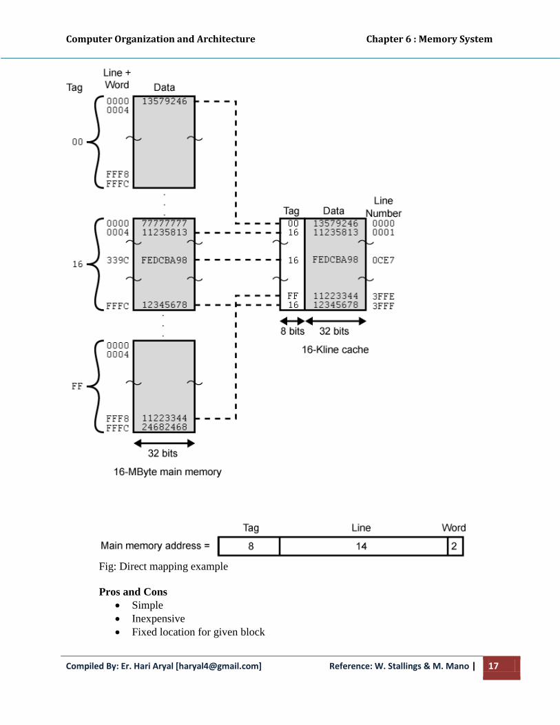
Computer Organization and Architecture Chapter 6 : Memory System
Compiled By: Er. Hari Aryal [[email protected]] Reference: W. Stallings & M. Mano | 17
Fig: Direct mapping example
Pros and Cons
Simple
Inexpensive
Fixed location for given block
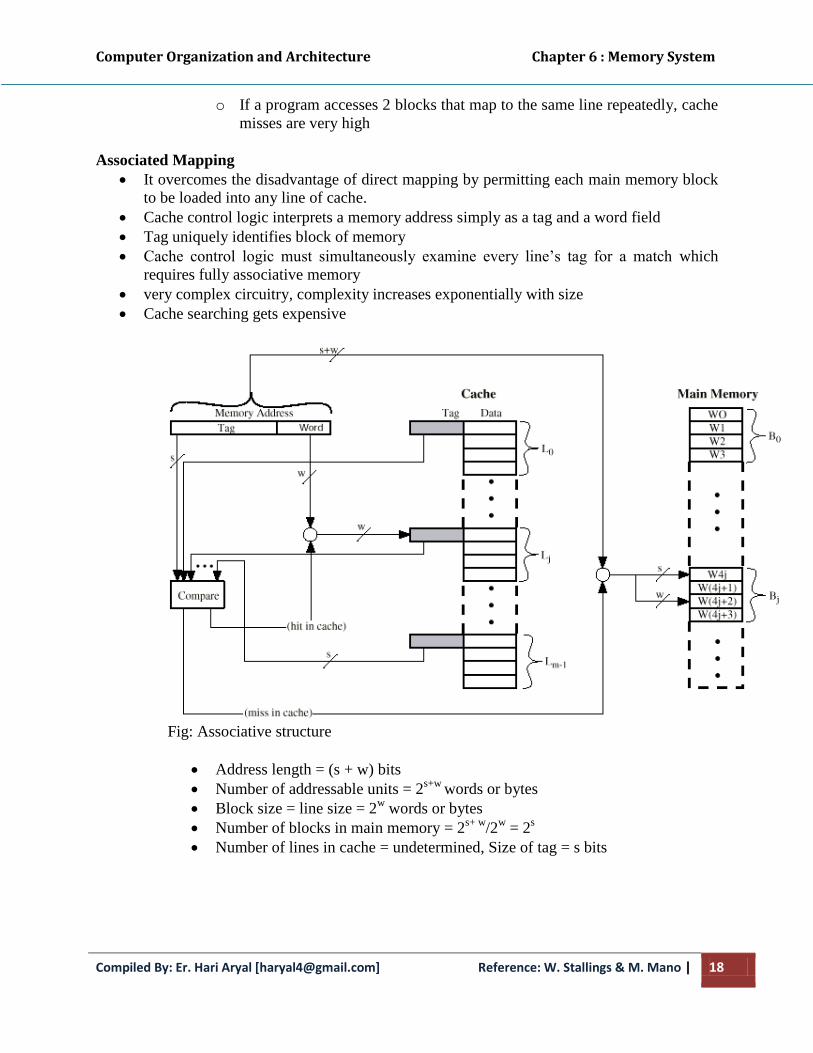
Computer Organization and Architecture Chapter 6 : Memory System
Compiled By: Er. Hari Aryal [[email protected]] Reference: W. Stallings & M. Mano | 18
o If a program accesses 2 blocks that map to the same line repeatedly, cache
misses are very high
Associated Mapping
It overcomes the disadvantage of direct mapping by permitting each main memory block
to be loaded into any line of cache.
Cache control logic interprets a memory address simply as a tag and a word field
Tag uniquely identifies block of memory
Cache control logic must simultaneously examine every line’s tag for a match which
requires fully associative memory
very complex circuitry, complexity increases exponentially with size
Cache searching gets expensive
Fig: Associative structure
Address length = (s + w) bits
Number of addressable units = 2s+w
words or bytes
Block size = line size = 2w words or bytes
Number of blocks in main memory = 2s+ w
/2w = 2
s
Number of lines in cache = undetermined, Size of tag = s bits
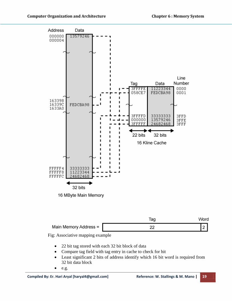
Computer Organization and Architecture Chapter 6 : Memory System
Compiled By: Er. Hari Aryal [[email protected]] Reference: W. Stallings & M. Mano | 19
Fig: Associative mapping example
22 bit tag stored with each 32 bit block of data
Compare tag field with tag entry in cache to check for hit
Least significant 2 bits of address identify which 16 bit word is required from
32 bit data block
e.g.
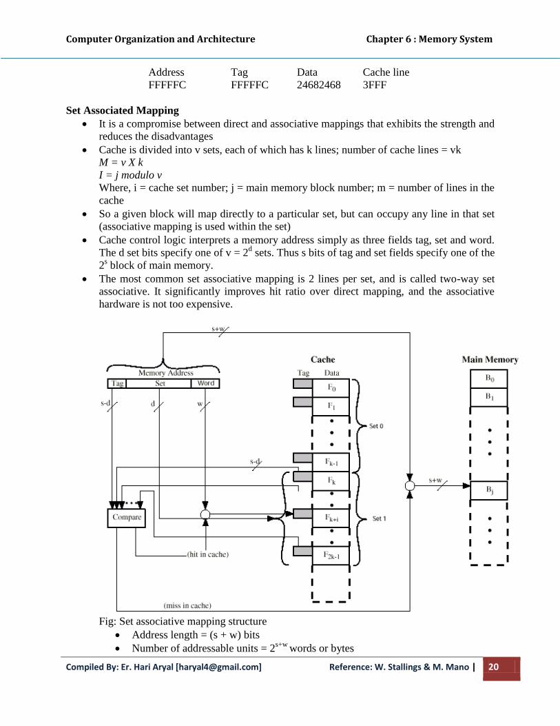
Computer Organization and Architecture Chapter 6 : Memory System
Compiled By: Er. Hari Aryal [[email protected]] Reference: W. Stallings & M. Mano | 20
Address Tag Data Cache line
FFFFFC FFFFFC 24682468 3FFF
Set Associated Mapping
It is a compromise between direct and associative mappings that exhibits the strength and
reduces the disadvantages
Cache is divided into v sets, each of which has k lines; number of cache lines = vk
M = v X k
I = j modulo v
Where, i = cache set number; j = main memory block number; m = number of lines in the
cache
So a given block will map directly to a particular set, but can occupy any line in that set
(associative mapping is used within the set)
Cache control logic interprets a memory address simply as three fields tag, set and word.
The d set bits specify one of v = 2d sets. Thus s bits of tag and set fields specify one of the
2s block of main memory.
The most common set associative mapping is 2 lines per set, and is called two-way set
associative. It significantly improves hit ratio over direct mapping, and the associative
hardware is not too expensive.
Fig: Set associative mapping structure
Address length = (s + w) bits
Number of addressable units = 2s+w
words or bytes
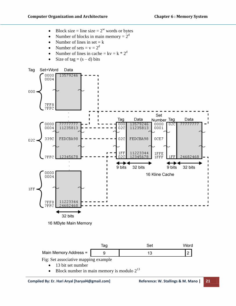
Computer Organization and Architecture Chapter 6 : Memory System
Compiled By: Er. Hari Aryal [[email protected]] Reference: W. Stallings & M. Mano | 21
Block size = line size = 2w words or bytes
Number of blocks in main memory = 2d
Number of lines in set = k
Number of sets = v = 2d
Number of lines in cache = kv = k * 2d
Size of tag = (s – d) bits
Fig: Set associative mapping example
13 bit set number
Block number in main memory is modulo 213

Computer Organization and Architecture Chapter 6 : Memory System
Compiled By: Er. Hari Aryal [[email protected]] Reference: W. Stallings & M. Mano | 22
000000, 00A000, 00B000, 00C000 … map to same set
Use set field to determine cache set to look in
Compare tag field to see if we have a hit
e.g
Address Tag Data Set number
1FF 7FFC 1FF 12345678 1FFF
001 7FFC 001 11223344 1FFF
6.6.3 Replacement algorithm
When all lines are occupied, bringing in a new block requires that an existing line be
overwritten.
Direct mapping
No choice possible with direct mapping
Each block only maps to one line
Replace that line
Associative and Set Associative mapping
Algorithms must be implemented in hardware for speed
Least Recently used (LRU)
o replace that block in the set which has been in cache longest with no
reference to it
o Implementation: with 2-way set associative, have a USE bit for each line
in a set. When a block is read into cache, use the line whose USE bit is set
to 0, then set its USE bit to one and the other line’s USE bit to 0.
o Probably the most effective method
First in first out (FIFO)
o replace that block in the set which has been in the cache longest
o Implementation: use a round-robin or circular buffer technique (keep up
with which slot’s “turn” is next
Least-frequently-used (LFU)
o replace that block in the set which has experienced the fewest references
or hits
o Implementation: associate a counter with each slot and increment when
used
Random
o replace a random block in the set
o Interesting because it is only slightly inferior to algorithms based on usage
Computer Organization and Architecture Chapter 6 : Memory System
Compiled By: Er. Hari Aryal [[email protected]] Reference: W. Stallings & M. Mano | 23
6.6.4 Write policy
When a line is to be replaced, must update the original copy of the line in main
memory if any addressable unit in the line has been changed
If a block has been altered in cache, it is necessary to write it back out to main
memory before replacing it with another block (writes are about 15% of memory
references)
Must not overwrite a cache block unless main memory is up to date
I/O modules may be able to read/write directly to memory
Multiple CPU’s may be attached to the same bus, each with their own cache
Write Through
All write operations are made to main memory as well as to cache, so main
memory is always valid
Other CPU’s monitor traffic to main memory to update their caches when needed
This generates substantial memory traffic and may create a bottleneck
Anytime a word in cache is changed, it is also changed in main memory
Both copies always agree
Generates lots of memory writes to main memory
Multiple CPUs can monitor main memory traffic to keep local (to CPU) cache up
to date
Lots of traffic
Slows down writes
Remember bogus write through caches!
Write back
When an update occurs, an UPDATE bit associated with that slot is set, so when
the block is replaced it is written back first
During a write, only change the contents of the cache
Update main memory only when the cache line is to be replaced
Causes “cache coherency” problems -- different values for the contents of an
address are in the cache and the main memory
Complex circuitry to avoid this problem
Accesses by I/O modules must occur through the cache
Multiple caches still can become invalidated, unless some cache coherency
system is used. Such systems include:
o Bus Watching with Write Through - other caches monitor memory writes
by other caches (using write through) and invalidates their own cache line
if a match
o Hardware Transparency - additional hardware links multiple caches so
that writes to one cache are made to the others
o Non-cacheable Memory - only a portion of main memory is shared by
more than one processor, and it is non-cacheable
Computer Organization and Architecture Chapter 6 : Memory System
Compiled By: Er. Hari Aryal [[email protected]] Reference: W. Stallings & M. Mano | 24
6.6.5 Number of caches
L1 and L2 Cache
On-chip cache (L1 Cache)
It is the cache memory on the same chip as the processor, the on-chip cache. It
reduces the processor's external bus activity and therefore speeds up execution
times and increases overall system performance.
Requires no bus operation for cache hits
Short data paths and same speed as other CPU transactions
Off-chip cache (L2 Cache)
It is the external cache which is beyond the processor. If there is no L2 cache and
processor makes an access request for memory location not in the L1 cache, then
processor must access DRAM or ROM memory across the bus. Due to this
typically slow bus speed and slow memory access time, this results in poor
performance. On the other hand, if an L2 SRAM cache is used, then frequently
the missing information can be quickly retrieved.
It can be much larger
It can be used with a local bus to buffer the CPU cache-misses from the system
bus
Unified and Split Cache
Unified Cache
o Single cache contains both instructions and data. Cache is flexible and can
balance “allocation” of space to instructions or data to best fit the
execution of the program.
o Has a higher hit rate than split cache, because it automatically balances
load between data and instructions (if an execution pattern involves more
instruction fetches than data fetches, the cache will fill up with more
instructions than data)
o Only one cache need be designed and implemented
Split Cache
o Cache splits into two parts first for instruction and second for data. Can
outperform unified cache in systems that support parallel execution and
pipelining (reduces cache contention)
o Trend is toward split cache because of superscalar CPU’s
o Better for pipelining, pre-fetching, and other parallel instruction execution
designs
o Eliminates cache contention between instruction processor and the
execution unit (which uses data)

Computer Organization and Architecture Chapter 7 : Input-Output Organization
Compiled By: Er. Hari Aryal [[email protected]] Reference: M. Mano & W. Stallings | 1
Chapter – 7
Input-Output organization
7.1 Peripheral devices
In addition to the processor and a set of memory modules, the third key element of a
computer system is a set of input-output subsystem referred to as I/O, provides an
efficient mode of communication between the central system and the outside
environment.
Programs and data must be entered into computer memory for processing and results
obtained from computations must be recorded or displayed for the user.
Devices that are under the direct control of the computer are said to be connected on-
line. These devices are designed to read information into or out of the memory unit
upon command from CPU.
Input or output devices attached to the computer are also called peripherals.
Among the most common peripherals are keyboards, display units, and printers.
Perhaps those provide auxiliary storage for the systems are magnetic disks and tapes.
Peripherals are electromechanical and electromagnetic devices of some complexity.
We can broadly classify peripheral devices into three categories:
o Human Readable: Communicating with the computer users, e.g. video
display terminal, printers etc.
o Machine Readable: Communicating with equipments, e.g. magnetic disk,
magnetic tape, sensor, actuators used in robotics etc.
o Communication: Communicating with remote devices means exchanging
data with that, e.g. modem, NIC (network interface Card) etc.
Fig: Block diagram of Peripheral device
Control signals determine the function that the device will perform such as send
data to I/O module, accept data from I/O module.
Status signals indicate the state of the device i.e. device is ready or not.
Data bits are actual data transformation.
Computer Organization and Architecture Chapter 7 : Input-Output Organization
Compiled By: Er. Hari Aryal [[email protected]] Reference: M. Mano & W. Stallings | 2
Control logic associated with the device controls the device's operation in
response to direction from the I/O module.
The transducer converts data from electrical to other forms of energy during
output and from other forms to electrical during input.
Buffer is associated with the transducer to temporarily hold data being transferred
between the I/O module and external devices i.e. peripheral environment.
Input Device
Keyboard
Optical input devices
o Card Reader
o Paper Tape Reader
o Optical Character Recognition (OCR)
o Optical Bar code reader (OBR)
o Digitizer
o Optical Mark Reader
Magnetic Input Devices
o Magnetic Stripe Reader
o Magnetic Ink Character Recognition (MICR)
Screen Input Devices
o Touch Screen
o Light Pen
o Mouse
Analog Input Devices
Output Device
Card Puncher, Paper Tape Puncher
Monitor (CRT, LCD, LED)
Printer (Impact, Ink Jet, Laser, Dot Matrix)
Plotter
Analog
Voice
7.2 I/O modules
I/O modules interface to the system bus or central switch (CPU and Memory), interfaces
and controls to one or more peripheral devices. I/O operations are accomplished through
a wide assortment of external devices that provide a means of exchanging data between
external environment and computer by a link to an I/O module. The link is used to
exchange control status and data between I/O module and the external devices.
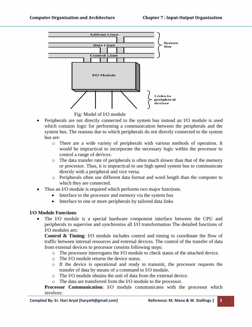
Computer Organization and Architecture Chapter 7 : Input-Output Organization
Compiled By: Er. Hari Aryal [[email protected]] Reference: M. Mano & W. Stallings | 3
Fig: Model of I/O module
Peripherals are not directly connected to the system bus instead an I/O module is used
which contains logic for performing a communication between the peripherals and the
system bus. The reasons due to which peripherals do not directly connected to the system
bus are:
o There are a wide variety of peripherals with various methods of operation. It
would be impractical to incorporate the necessary logic within the processor to
control a range of devices.
o The data transfer rate of peripherals is often much slower than that of the memory
or processor. Thus, it is impractical to use high speed system bus to communicate
directly with a peripheral and vice versa.
o Peripherals often use different data format and word length than the computer to
which they are connected.
Thus an I/O module is required which performs two major functions.
Interface to the processor and memory via the system bus
Interface to one or more peripherals by tailored data links
I/O Module Functions
The I/O module is a special hardware component interface between the CPU and
peripherals to supervise and synchronize all I/O transformation The detailed functions of
I/O modules are;
Control & Timing: I/O module includes control and timing to coordinate the flow of
traffic between internal resources and external devices. The control of the transfer of data
from external devices to processor consists following steps:
o The processor interrogates the I/O module to check status of the attached device.
o The I/O module returns the device status.
o If the device is operational and ready to transmit, the processor requests the
transfer of data by means of a command to I/O module.
o The I/O module obtains the unit of data from the external device.
o The data are transferred from the I/O module to the processor.
Processor Communication: I/O module communicates with the processor which
involves:

Computer Organization and Architecture Chapter 7 : Input-Output Organization
Compiled By: Er. Hari Aryal [[email protected]] Reference: M. Mano & W. Stallings | 4
o Command decoding: I/O module accepts commands from the processor.
o Data: Data are exchanged between the processor and I/O module over the bus.
o Status reporting: Peripherals are too slow and it is important to know the status of
I/O module.
o Address recognition: I/O module must recognize one unique address for each
peripheral it controls.
Device Communication: It involves commands, status information and data.
Data Buffering: I/O module must be able to operate at both device and memory speeds.
If the I/O device operates at a rate higher than the memory access rate, then the I/O
module performs data buffering. If I/O devices rate slower than memory, it buffers data
so as not to tie up the memory in slower transfer operation.
Error Detection: I/O module is responsible for error detection such as mechanical and
electrical malfunction reported by device e.g. paper jam, bad ink track & unintentional
changes to the bit pattern and transmission error.
I/O Module Structure
Fig: Block diagram of I/O Module
The I/O bus from the processor is attached to all peripheral interfaces
To communicate with the particular devices, the processor places a device address on the
address bus.
Each interface contains an address decoder that monitors the address line. When the
interface detects the particular device address, it activates the path between the data line
and devices that it controls.
At the same time that the address is made available in the address line, the processor
provides a function code in the control way includes control command, output data and
input data.
I/O Module Decisions
Hide or reveal device properties to CPU
Support multiple or single device

Computer Organization and Architecture Chapter 7 : Input-Output Organization
Compiled By: Er. Hari Aryal [[email protected]] Reference: M. Mano & W. Stallings | 5
Control device functions or leave for CPU
Also O/S decisions
o e.g. Unix treats everything it can as a file
7.3 Input-Output interface
Input-Output interface provides a method for transferring information between internal
storage (such as memory and CPU registers) and external I/O devices.
Peripherals connected to a computer need special communication links for interfacing
them with the central processing unit.
The communication link resolves the following differences between the computer and
peripheral devices.
o Devices and signals
Peripherals - Electromechanical Devices
CPU or Memory - Electronic Device
o Data Transfer Rate
Peripherals - Usually slower
CPU or Memory - Usually faster than peripherals
Some kinds of Synchronization mechanism may be needed
o Unit of Information
Peripherals - Byte
CPU or Memory - Word
o Operating Modes
Peripherals - Autonomous, Asynchronous
CPU or Memory – Synchronous
To resolve these differences, computer systems include special hardware components
(Interfaces) between the CPU and peripherals to supervise and synchronize all input and
output interfaces.
I/O Bus and Interface Modules
The I/O bus consists of data lines, address lines and control lines.
Fig: Connection of I/O bus to input-output devices
Interface performs the following:
o Decodes the device address (device code)
o Decodes the commands (operation)
o Provides signals for the peripheral controller

Computer Organization and Architecture Chapter 7 : Input-Output Organization
Compiled By: Er. Hari Aryal [[email protected]] Reference: M. Mano & W. Stallings | 6
o Synchronizes the data flow and supervises the transfer rate between peripheral
and CPU or Memory
I/O commands that the interface may receive:
o Control command: issued to activate the peripheral and to inform it what to do.
o Status command: used to test various status conditions in the interface and the
peripheral.
o Output data: causes the interface to respond by transferring data from the bus into
one of its registers.
o Input data: is the opposite of the data output.
I/O versus Memory Bus
Computer buses can be used to communicate with memory and I/O in three ways:
o Use two separate buses, one for memory and other for I/O. In this method, all
data, address and control lines would be separate for memory and I/O.
o Use one common bus for both memory and I/O but have separate control lines.
There is a separate read and write lines; I/O read and I/O write for I/O and
memory read and memory write for memory.
o Use a common bus for memory and I/O with common control line. This I/O
configuration is called memory mapped.
Isolated I/O versus Memory Mapped I/O
Isolated I/O
o Separate I/O read/write control lines in addition to memory read/write control lines
o Separate (isolated) memory and I/O address spaces
o Distinct input and output instructions
Memory-mapped I/O o A single set of read/write control lines (no distinction between memory and I/O
transfer)
o Memory and I/O addresses share the common address space which reduces memory
address range available
o No specific input or output instruction so the same memory reference instructions can
be used for I/O transfers
o Considerable flexibility in handling I/O operations
Example of I/O Interface
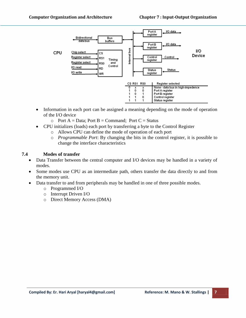
Computer Organization and Architecture Chapter 7 : Input-Output Organization
Compiled By: Er. Hari Aryal [[email protected]] Reference: M. Mano & W. Stallings | 7
Information in each port can be assigned a meaning depending on the mode of operation
of the I/O device
o Port A = Data; Port B = Command; Port C = Status
CPU initializes (loads) each port by transferring a byte to the Control Register
o Allows CPU can define the mode of operation of each port
o Programmable Port: By changing the bits in the control register, it is possible to
change the interface characteristics
7.4 Modes of transfer
Data Transfer between the central computer and I/O devices may be handled in a variety of
modes.
Some modes use CPU as an intermediate path, others transfer the data directly to and from
the memory unit.
Data transfer to and from peripherals may be handled in one of three possible modes.
o Programmed I/O
o Interrupt Driven I/O
o Direct Memory Access (DMA)
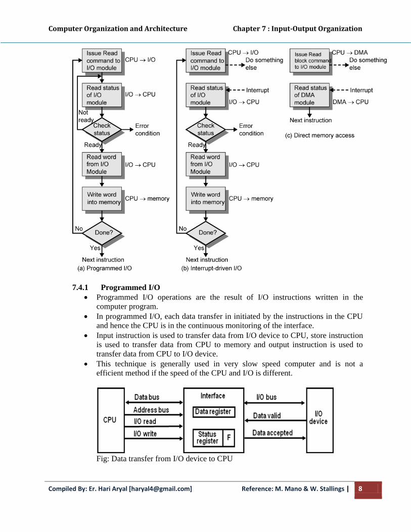
Computer Organization and Architecture Chapter 7 : Input-Output Organization
Compiled By: Er. Hari Aryal [[email protected]] Reference: M. Mano & W. Stallings | 8
7.4.1 Programmed I/O
Programmed I/O operations are the result of I/O instructions written in the
computer program.
In programmed I/O, each data transfer in initiated by the instructions in the CPU
and hence the CPU is in the continuous monitoring of the interface.
Input instruction is used to transfer data from I/O device to CPU, store instruction
is used to transfer data from CPU to memory and output instruction is used to
transfer data from CPU to I/O device.
This technique is generally used in very slow speed computer and is not a
efficient method if the speed of the CPU and I/O is different.
Fig: Data transfer from I/O device to CPU
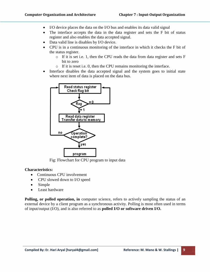
Computer Organization and Architecture Chapter 7 : Input-Output Organization
Compiled By: Er. Hari Aryal [[email protected]] Reference: M. Mano & W. Stallings | 9
I/O device places the data on the I/O bus and enables its data valid signal
The interface accepts the data in the data register and sets the F bit of status
register and also enables the data accepted signal.
Data valid line is disables by I/O device.
CPU is in a continuous monitoring of the interface in which it checks the F bit of
the status register.
o If it is set i.e. 1, then the CPU reads the data from data register and sets F
bit to zero
o If it is reset i.e. 0, then the CPU remains monitoring the interface.
Interface disables the data accepted signal and the system goes to initial state
where next item of data is placed on the data bus.
Fig: Flowchart for CPU program to input data
Characteristics:
Continuous CPU involvement
CPU slowed down to I/O speed
Simple
Least hardware
Polling, or polled operation, in computer science, refers to actively sampling the status of an
external device by a client program as a synchronous activity. Polling is most often used in terms
of input/output (I/O), and is also referred to as polled I/O or software driven I/O.

Computer Organization and Architecture Chapter 7 : Input-Output Organization
Compiled By: Er. Hari Aryal [[email protected]] Reference: M. Mano & W. Stallings | 10
7.4.2 Interrupt-driven I/O
Polling takes valuable CPU time
Open communication only when some data has to be passed -> Interrupt.
I/O interface, instead of the CPU, monitors the I/O device
When the interface determines that the I/O device is ready for data transfer, it
generates an Interrupt Request to the CPU
Upon detecting an interrupt, CPU stops momentarily the task it is doing, branches
to the service routine to process the data transfer, and then returns to the task it
was performing
The problem with programmed I/O is that the processor has to wait a long time for
the I/O module of concern to be ready for either reception or transmission of data.
The processor, while waiting, must repeatedly interrogate the status of the I/O
module. As a result, the level of the performance of the entire system is severely
degraded. An alternative is for the processor to issue an I/O command to a module
and then go on to do some other useful work. The I/O module will then interrupt the
processor to request service when it is ready to exchange data with processor. The
processor then executes the data transfer, and then resumes its former processing. The
interrupt can be initiated either by software or by hardware.
Interrupt Driven I/O basic operation
CPU issues read command
I/O module gets data from peripheral whilst CPU does other work
I/O module interrupts CPU
CPU requests data
I/O module transfers data
Interrupt Processing from CPU viewpoint
Issue read command
Do other work
Check for interrupt at end of each instruction cycle
If interrupted:-
o Save context (registers)
o Process interrupt
o Fetch data & store

Computer Organization and Architecture Chapter 7 : Input-Output Organization
Compiled By: Er. Hari Aryal [[email protected]] Reference: M. Mano & W. Stallings | 11
Fig: Simple Interrupt Processing
Priority Interrupt
Determines which interrupt is to be served first when two or more requests are
made simultaneously
Also determines which interrupts are permitted to interrupt the computer while
another is being serviced
Higher priority interrupts can make requests while servicing a lower priority
interrupt
Priority Interrupt by Software (Polling)
Priority is established by the order of polling the devices (interrupt sources), that
is identify the highest-priority source by software means
One common branch address is used for all interrupts
Program polls the interrupt sources in sequence
The highest-priority source is tested first
Flexible since it is established by software
Low cost since it needs a very little hardware
Very slow
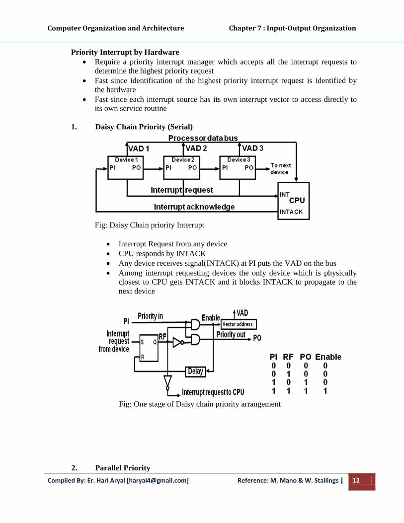
Computer Organization and Architecture Chapter 7 : Input-Output Organization
Compiled By: Er. Hari Aryal [[email protected]] Reference: M. Mano & W. Stallings | 12
Priority Interrupt by Hardware
Require a priority interrupt manager which accepts all the interrupt requests to
determine the highest priority request
Fast since identification of the highest priority interrupt request is identified by
the hardware
Fast since each interrupt source has its own interrupt vector to access directly to
its own service routine
1. Daisy Chain Priority (Serial)
Fig: Daisy Chain priority Interrupt
Interrupt Request from any device
CPU responds by INTACK
Any device receives signal(INTACK) at PI puts the VAD on the bus
Among interrupt requesting devices the only device which is physically
closest to CPU gets INTACK and it blocks INTACK to propagate to the
next device
Fig: One stage of Daisy chain priority arrangement
2. Parallel Priority

Computer Organization and Architecture Chapter 7 : Input-Output Organization
Compiled By: Er. Hari Aryal [[email protected]] Reference: M. Mano & W. Stallings | 13
Fig: Parallel priority interrupts hardware
IEN: Set or Clear by instructions ION or IOF
IST: Represents an unmasked interrupt has occurred. INTACK enables
tristate Bus Buffer to load VAD generated by the Priority Logic
Interrupt Register:
o Each bit is associated with an Interrupt Request from different
Interrupt Source - different priority level
o Each bit can be cleared by a program instruction
Mask Register:
o Mask Register is associated with Interrupt Register
o Each bit can be set or cleared by an Instruction
Priority Encoder
Determines the highest priority interrupt when more than one interrupts take place
Fig: Priority Encoder Truth Table
Interrupt Cycle
At the end of each Instruction cycle
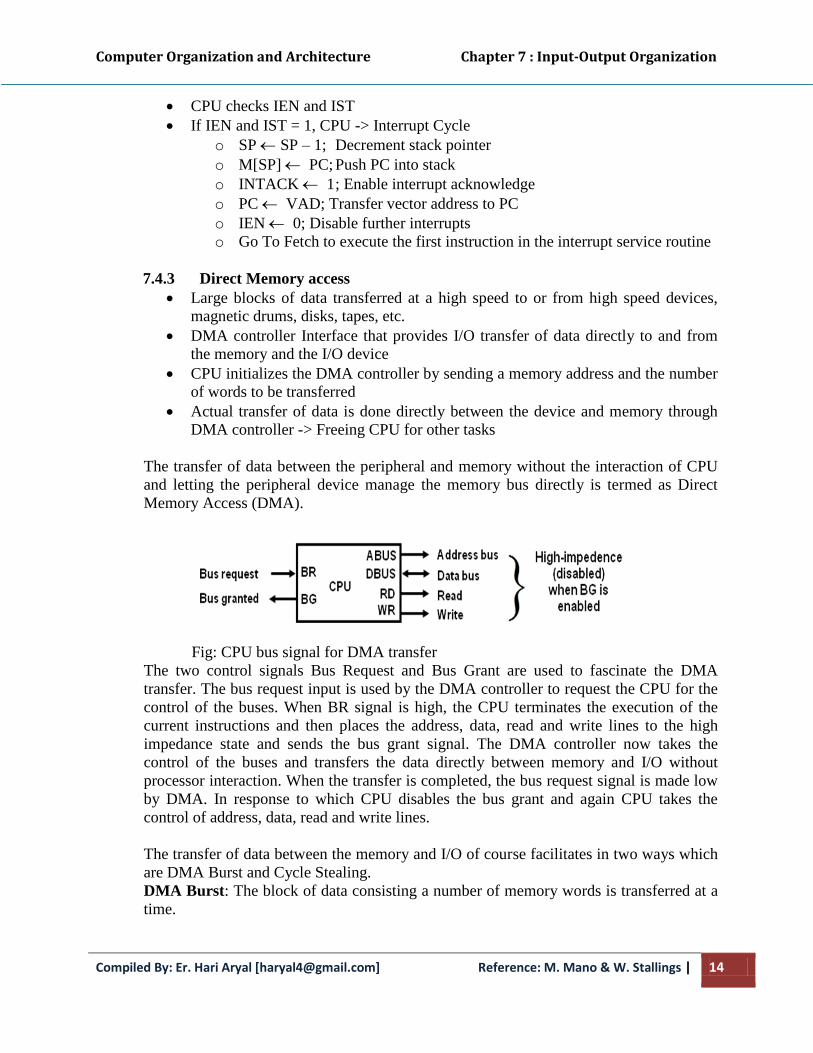
Computer Organization and Architecture Chapter 7 : Input-Output Organization
Compiled By: Er. Hari Aryal [[email protected]] Reference: M. Mano & W. Stallings | 14
CPU checks IEN and IST
If IEN and IST = 1, CPU -> Interrupt Cycle
o SP SP – 1; Decrement stack pointer
o M[SP] PC; Push PC into stack
o INTACK 1 ; Enable interrupt acknowledge
o PC VAD; Transfer vector address to PC
o IEN 0; Disable further interrupts
o Go To Fetch to execute the first instruction in the interrupt service routine
7.4.3 Direct Memory access
Large blocks of data transferred at a high speed to or from high speed devices,
magnetic drums, disks, tapes, etc.
DMA controller Interface that provides I/O transfer of data directly to and from
the memory and the I/O device
CPU initializes the DMA controller by sending a memory address and the number
of words to be transferred
Actual transfer of data is done directly between the device and memory through
DMA controller -> Freeing CPU for other tasks
The transfer of data between the peripheral and memory without the interaction of CPU
and letting the peripheral device manage the memory bus directly is termed as Direct
Memory Access (DMA).
Fig: CPU bus signal for DMA transfer
The two control signals Bus Request and Bus Grant are used to fascinate the DMA
transfer. The bus request input is used by the DMA controller to request the CPU for the
control of the buses. When BR signal is high, the CPU terminates the execution of the
current instructions and then places the address, data, read and write lines to the high
impedance state and sends the bus grant signal. The DMA controller now takes the
control of the buses and transfers the data directly between memory and I/O without
processor interaction. When the transfer is completed, the bus request signal is made low
by DMA. In response to which CPU disables the bus grant and again CPU takes the
control of address, data, read and write lines.
The transfer of data between the memory and I/O of course facilitates in two ways which
are DMA Burst and Cycle Stealing.
DMA Burst: The block of data consisting a number of memory words is transferred at a
time.
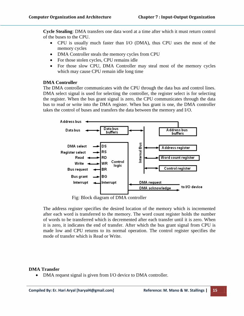
Computer Organization and Architecture Chapter 7 : Input-Output Organization
Compiled By: Er. Hari Aryal [[email protected]] Reference: M. Mano & W. Stallings | 15
Cycle Stealing: DMA transfers one data word at a time after which it must return control
of the buses to the CPU.
CPU is usually much faster than I/O (DMA), thus CPU uses the most of the
memory cycles
DMA Controller steals the memory cycles from CPU
For those stolen cycles, CPU remains idle
For those slow CPU, DMA Controller may steal most of the memory cycles
which may cause CPU remain idle long time
DMA Controller
The DMA controller communicates with the CPU through the data bus and control lines.
DMA select signal is used for selecting the controller, the register select is for selecting
the register. When the bus grant signal is zero, the CPU communicates through the data
bus to read or write into the DMA register. When bus grant is one, the DMA controller
takes the control of buses and transfers the data between the memory and I/O.
Fig: Block diagram of DMA controller
The address register specifies the desired location of the memory which is incremented
after each word is transferred to the memory. The word count register holds the number
of words to be transferred which is decremented after each transfer until it is zero. When
it is zero, it indicates the end of transfer. After which the bus grant signal from CPU is
made low and CPU returns to its normal operation. The control register specifies the
mode of transfer which is Read or Write.
DMA Transfer
DMA request signal is given from I/O device to DMA controller.

Computer Organization and Architecture Chapter 7 : Input-Output Organization
Compiled By: Er. Hari Aryal [[email protected]] Reference: M. Mano & W. Stallings | 16
DMA sends the bus request signal to CPU in response to which CPU disables its current
instructions and initialize the DMA by sending the following information.
o The starting address of the memory block where the data are available (for read)
and where data to be stored (for write)
o The word count which is the number of words in the memory block
o Control to specify the mode of transfer
o Sends a bust grant as 1 so that DMA controller can take the control of the buses
o DMA sends the DMA acknowledge signal in response to which peripheral device
puts the words in the data bus (for write) or receives a word from the data bus (for
read).
Fig: DMA transfer in a computer system
DMA Operation
CPU tells DMA controller:-
o Read/Write
o Device address
o Starting address of memory block for data
o Amount of data to be transferred
CPU carries on with other work
DMA controller deals with transfer
DMA controller sends interrupt when finished
7.5 I/O Processors
Processor with direct memory access capability that communicates with I/O devices
Channel accesses memory by cycle stealing
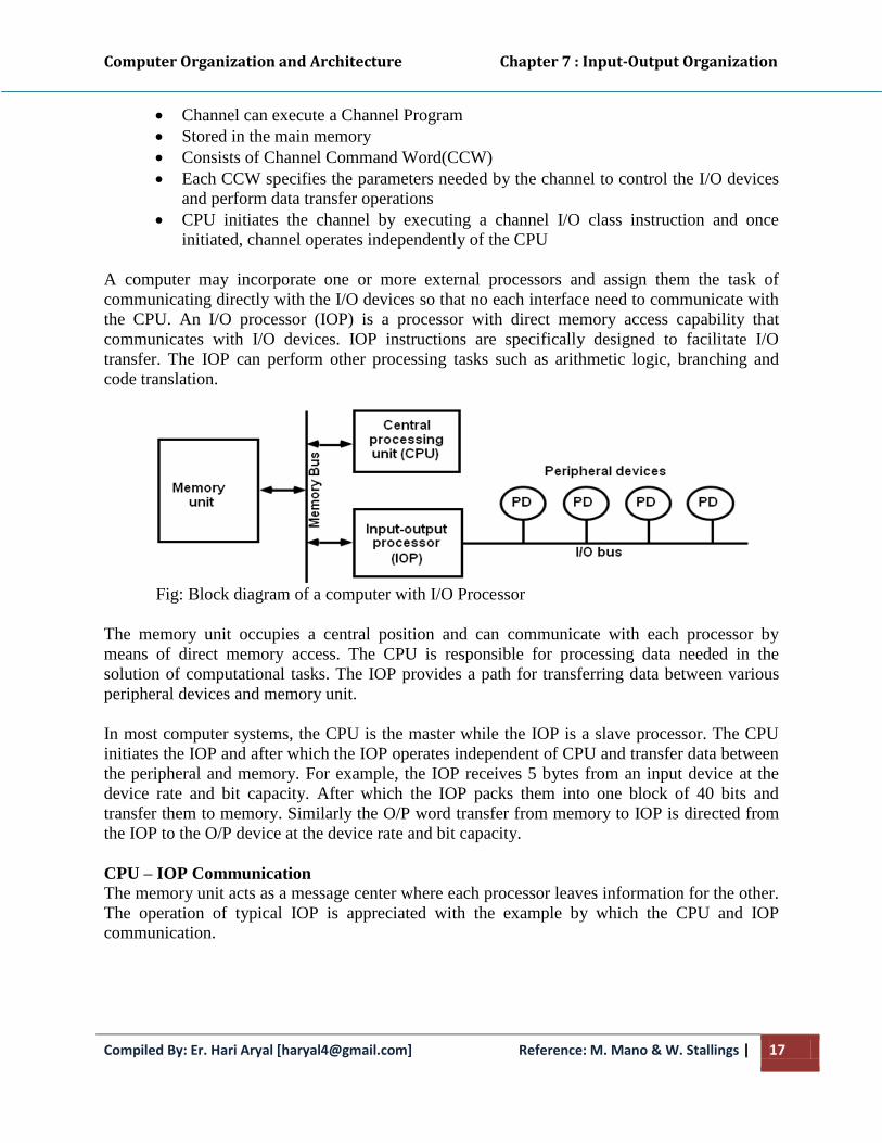
Computer Organization and Architecture Chapter 7 : Input-Output Organization
Compiled By: Er. Hari Aryal [[email protected]] Reference: M. Mano & W. Stallings | 17
Channel can execute a Channel Program
Stored in the main memory
Consists of Channel Command Word(CCW)
Each CCW specifies the parameters needed by the channel to control the I/O devices
and perform data transfer operations
CPU initiates the channel by executing a channel I/O class instruction and once
initiated, channel operates independently of the CPU
A computer may incorporate one or more external processors and assign them the task of
communicating directly with the I/O devices so that no each interface need to communicate with
the CPU. An I/O processor (IOP) is a processor with direct memory access capability that
communicates with I/O devices. IOP instructions are specifically designed to facilitate I/O
transfer. The IOP can perform other processing tasks such as arithmetic logic, branching and
code translation.
Fig: Block diagram of a computer with I/O Processor
The memory unit occupies a central position and can communicate with each processor by
means of direct memory access. The CPU is responsible for processing data needed in the
solution of computational tasks. The IOP provides a path for transferring data between various
peripheral devices and memory unit.
In most computer systems, the CPU is the master while the IOP is a slave processor. The CPU
initiates the IOP and after which the IOP operates independent of CPU and transfer data between
the peripheral and memory. For example, the IOP receives 5 bytes from an input device at the
device rate and bit capacity. After which the IOP packs them into one block of 40 bits and
transfer them to memory. Similarly the O/P word transfer from memory to IOP is directed from
the IOP to the O/P device at the device rate and bit capacity.
CPU – IOP Communication
The memory unit acts as a message center where each processor leaves information for the other.
The operation of typical IOP is appreciated with the example by which the CPU and IOP
communication.

Computer Organization and Architecture Chapter 7 : Input-Output Organization
Compiled By: Er. Hari Aryal [[email protected]] Reference: M. Mano & W. Stallings | 18
Fig: CPU – IOP communication
The CPU sends an instruction to test the IOP path.
The IOP responds by inserting a status word in memory for the CPU to check.
The bits of the status word indicate the condition of the IOP and I/O device, such as IOP
overload condition, device busy with another transfer or device ready for I/O transfer.
The CPU refers to the status word in in memory to decide what to do next.
If all right up to this, the CPU sends the instruction to start I/O transfer.
The CPU now continues with another program while IOP is busy with I/O program.
When IOP terminates the execution, it sends an interrupt request to CPU.
CPU responds by issuing an instruction to read the status from the IOP.
IOP responds by placing the contents to its status report into specified memory location.
Status word indicates whether the transfer has been completed or with error.
7.6 Data Communication Processor
Distributes and collects data from many remote terminals connected through
telephone and other communication lines.
Transmission:
o Synchronous
o Asynchronous
Transmission Error:
o Parity
o Checksum
o Cyclic Redundancy Check
Computer Organization and Architecture Chapter 7 : Input-Output Organization
Compiled By: Er. Hari Aryal [[email protected]] Reference: M. Mano & W. Stallings | 19
o Longitudinal Redundancy Check
Transmission Modes:
o Simples
o Half Duplex
o Full Duplex
Data Link & Protocol
A data communication (command) processor is an I/O processor that distributes and collects data
from remote terminals connected through telephone and other communication lines. In processor
communication, processor communicates with the I/O device through a common bus i.e. data
and control with sharing by each peripherals. In data communication, processor communicates
with each terminal through a single pair of wires.
The way that remote terminals are connected to a data communication processor is via telephone
lines or other public or private communication facilities. The data communication may be either
through synchronous transmission or through asynchronous transmission. One of the functions of
data communication processor is check for transmission errors. An error can be detected by
checking the parity in each character received. The other ways are checksum, longitudinal
redundancy check (LRC) and cyclic redundancy check (CRC).
Data can be transmitted between two points through three different modes. First is simplex
where data can be transmitted in only one direction such as TV broadcasting. Second is half
duplex where data can be transmitted in both directions at a time such as walkie-talkie. The third
is full duplex where data can be transmitted in both directions simultaneously such as telephone.
The communication lines, modems and other equipment used in the transmission of information
between two or more stations is called data link. The orderly transfer of information in a data
link is accomplished by means of a protocol.

Computer Organization and Architecture Chapter 8 : Multiprocessors
Compiled By: Er. Hari Aryal [[email protected]] Reference: M. Mano | 1
Chapter – 8
Multiprocessors
8.1 Characteristics of multiprocessors
A multiprocessor system is an interconnection of two or more CPUs with memory
and input-output equipment.
The term “processor” in multiprocessor can mean either a central processing unit
(CPU) or an input-output processor (IOP).
Multiprocessors are classified as multiple instruction stream, multiple data stream
(MIMD) systems
The similarity and distinction between multiprocessor and multicomputer are
o Similarity
Both support concurrent operations
o Distinction
The network consists of several autonomous computers that may
or may not communicate with each other.
A multiprocessor system is controlled by one operating system that
provides interaction between processors and all the components of
the system cooperate in the solution of a problem.
Multiprocessing improves the reliability of the system.
The benefit derived from a multiprocessor organization is an improved system
performance.
o Multiple independent jobs can be made to operate in parallel.
o A single job can be partitioned into multiple parallel tasks.
Multiprocessing can improve performance by decomposing a program into
parallel executable tasks.
o The user can explicitly declare that certain tasks of the program be
executed in parallel.
This must be done prior to loading the program by specifying the
parallel executable segments.
o The other is to provide a compiler with multiprocessor software that can
automatically detect parallelism in a user’s program.
Multiprocessor are classified by the way their memory is organized.
o A multiprocessor system with common shared memory is classified as a
shared-memory or tightly coupled multiprocessor.
Tolerate a higher degree of interaction between tasks.
o Each processor element with its own private local memory is classified as
a distributed-memory or loosely coupled system.
Are most efficient when the interaction between tasks is minimal

Computer Organization and Architecture Chapter 8 : Multiprocessors
Compiled By: Er. Hari Aryal [[email protected]] Reference: M. Mano | 2
8.2 Interconnection Structures
The components that form a multiprocessor system are CPUs, IOPs connected to input-
output devices, and a memory unit.
The interconnection between the components can have different physical configurations,
depending on the number of transfer paths that are available
o Between the processors and memory in a shared memory system
o Among the processing elements in a loosely coupled system
There are several physical forms available for establishing an interconnection network.
o Time-shared common bus
o Multiport memory
o Crossbar switch
o Multistage switching network
o Hypercube system
Time Shared Common Bus
A common-bus multiprocessor system consists of a number of processors connected
through a common path to a memory unit.
Disadv.:
o Only one processor can communicate with the memory or another processor at
any given time.
o As a consequence, the total overall transfer rate within the system is limited by
the speed of the single path
A more economical implementation of a dual bus structure is depicted in Fig. below.
Part of the local memory may be designed as a cache memory attached to the CPU.
Fig: Time shared common bus organization

Computer Organization and Architecture Chapter 8 : Multiprocessors
Compiled By: Er. Hari Aryal [[email protected]] Reference: M. Mano | 3
Fig: System bus structure for multiprocessorsa
Multiport Memory
A multiport memory system employs separate buses between each memory module and
each CPU.
The module must have internal control logic to determine which port will have access to
memory at any given time.
Memory access conflicts are resolved by assigning fixed priorities to each memory port.
Adv.:
o The high transfer rate can be achieved because of the multiple paths.
Disadv.:
o It requires expensive memory control logic and a large number of cables and
connections
Fig: Multiport memory organization

Computer Organization and Architecture Chapter 8 : Multiprocessors
Compiled By: Er. Hari Aryal [[email protected]] Reference: M. Mano | 4
Crossbar Switch
Consists of a number of crosspoints that are placed at intersections between processor
buses and memory module paths.
The small square in each crosspoint is a switch that determines the path from a processor
to a memory module.
Adv.:
o Supports simultaneous transfers from all memory modules
Disadv.:
o The hardware required to implement the switch can become quite large and
complex.
Below fig. shows the functional design of a crossbar switch connected to one memory
module.
Fig: Crossbar switch
Fig: Block diagram of crossbar switch

Computer Organization and Architecture Chapter 8 : Multiprocessors
Compiled By: Er. Hari Aryal [[email protected]] Reference: M. Mano | 5
Multistage Switching Network
The basic component of a multistage network is a two-input, two-output interchange
switch as shown in Fig. below.
Using the 2x2 switch as a building block, it is possible to build a multistage network to
control the communication between a number of sources and destinations.
o To see how this is done, consider the binary tree shown in Fig. below.
o Certain request patterns cannot be satisfied simultaneously. i.e., if P1 000~011,
then P2 100~111
One such topology is the omega switching network shown in Fig. below
.
Fig: 8 x 8 Omega Switching Network
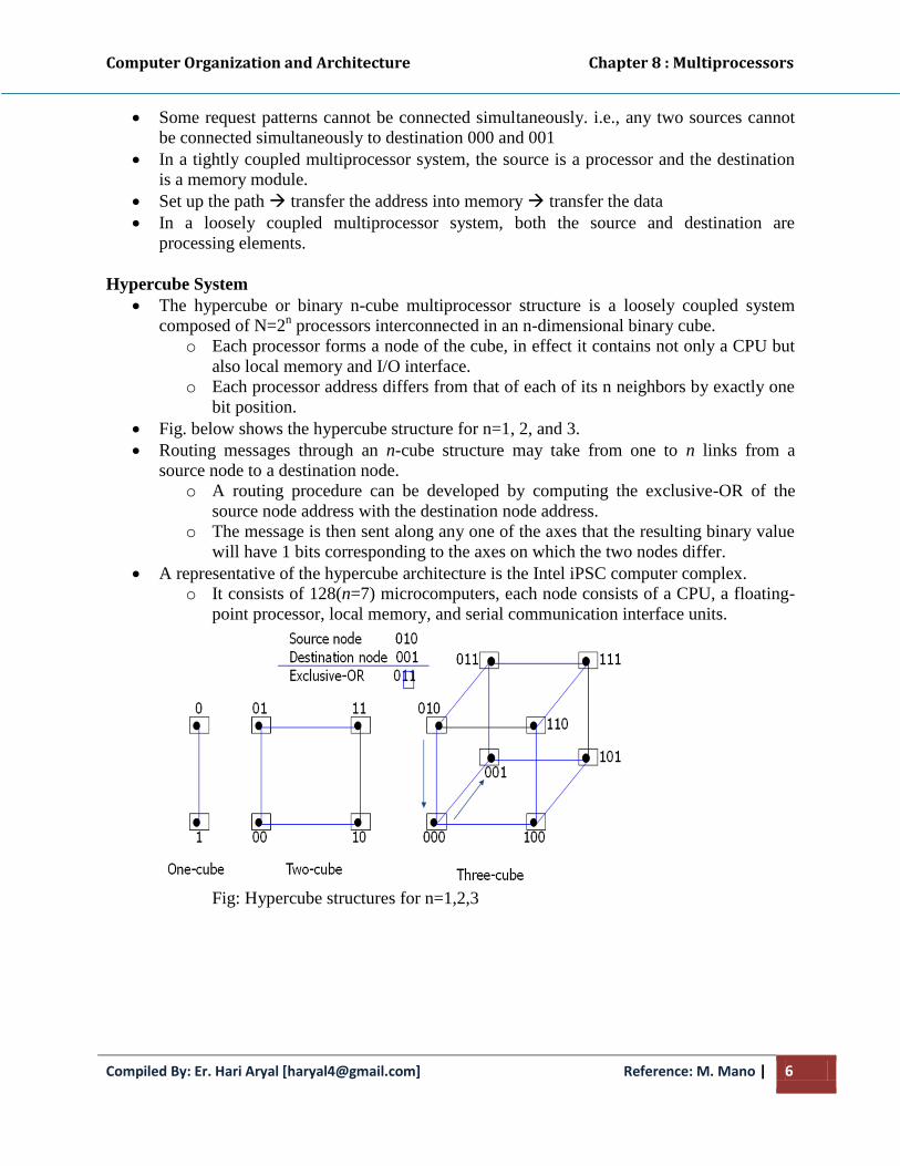
Computer Organization and Architecture Chapter 8 : Multiprocessors
Compiled By: Er. Hari Aryal [[email protected]] Reference: M. Mano | 6
Some request patterns cannot be connected simultaneously. i.e., any two sources cannot
be connected simultaneously to destination 000 and 001
In a tightly coupled multiprocessor system, the source is a processor and the destination
is a memory module.
Set up the path transfer the address into memory transfer the data
In a loosely coupled multiprocessor system, both the source and destination are
processing elements.
Hypercube System
The hypercube or binary n-cube multiprocessor structure is a loosely coupled system
composed of N=2n processors interconnected in an n-dimensional binary cube.
o Each processor forms a node of the cube, in effect it contains not only a CPU but
also local memory and I/O interface.
o Each processor address differs from that of each of its n neighbors by exactly one
bit position.
Fig. below shows the hypercube structure for n=1, 2, and 3.
Routing messages through an n-cube structure may take from one to n links from a
source node to a destination node.
o A routing procedure can be developed by computing the exclusive-OR of the
source node address with the destination node address.
o The message is then sent along any one of the axes that the resulting binary value
will have 1 bits corresponding to the axes on which the two nodes differ.
A representative of the hypercube architecture is the Intel iPSC computer complex.
o It consists of 128(n=7) microcomputers, each node consists of a CPU, a floating-
point processor, local memory, and serial communication interface units.
Fig: Hypercube structures for n=1,2,3

Computer Organization and Architecture Chapter 8 : Multiprocessors
Compiled By: Er. Hari Aryal [[email protected]] Reference: M. Mano | 7
8.3 Inter processor Communication and Synchronization
The various processors in a multiprocessor system must be provided with a facility for
communicating with each other.
o A communication path can be established through a portion of memory or a
common input-output channels.
The sending processor structures a request, a message, or a procedure, and places it in the
memory mailbox.
o Status bits residing in common memory
o The receiving processor can check the mailbox periodically.
o The response time of this procedure can be time consuming.
A more efficient procedure is for the sending processor to alert the receiving processor
directly by means of an interrupt signal.
In addition to shared memory, a multiprocessor system may have other shared resources.
e.g., a magnetic disk storage unit.
To prevent conflicting use of shared resources by several processors there must be a
provision for assigning resources to processors. i.e., operating system.
There are three organizations that have been used in the design of operating system for
multiprocessors: master-slave configuration, separate operating system, and distributed
operating system.
In a master-slave mode, one processor, master, always executes the operating system
functions.
In the separate operating system organization, each processor can execute the operating
system routines it needs. This organization is more suitable for loosely coupled systems.
In the distributed operating system organization, the operating system routines are
distributed among the available processors. However, each particular operating system
function is assigned to only one processor at a time. It is also referred to as a floating
operating system.
Loosely Coupled System
There is no shared memory for passing information.
The communication between processors is by means of message passing through I/O
channels.
The communication is initiated by one processor calling a procedure that resides in
the memory of the processor with which it wishes to communicate.
The communication efficiency of the interprocessor network depends on the
communication routing protocol, processor speed, data link speed, and the topology
of the network.
Interprocess Synchronization
The instruction set of a multiprocessor contains basic instructions that are used to
implement communication and synchronization between cooperating processes.
o Communication refers to the exchange of data between different processes.
o Synchronization refers to the special case where the data used to communicate
between processors is control information.
Computer Organization and Architecture Chapter 8 : Multiprocessors
Compiled By: Er. Hari Aryal [[email protected]] Reference: M. Mano | 8
Synchronization is needed to enforce the correct sequence of processes and to ensure
mutually exclusive access to shared writable data.
Multiprocessor systems usually include various mechanisms to deal with the
synchronization of resources.
o Low-level primitives are implemented directly by the hardware.
o These primitives are the basic mechanisms that enforce mutual exclusion for more
complex mechanisms implemented in software.
o A number of hardware mechanisms for mutual exclusion have been developed.
A binary semaphore
Mutual Exclusion with Semaphore
A properly functioning multiprocessor system must provide a mechanism that will
guarantee orderly access to shared memory and other shared resources.
o Mutual exclusion: This is necessary to protect data from being changed
simultaneously by two or more processors.
o Critical section: is a program sequence that must complete execution before
another processor accesses the same shared resource.
A binary variable called a semaphore is often used to indicate whether or not a processor
is executing a critical section.
Testing and setting the semaphore is itself a critical operation and must be performed as a
single indivisible operation.
A semaphore can be initialized by means of a test and set instruction in conjunction with
a hardware lock mechanism.
The instruction TSL SEM will be executed in two memory cycles (the first to read and
the second to write) as follows: R M[SEM], M[SEM] 1
Note that the lock signal must be active during the execution of the test-and-set
instruction.
Related Documents


