Chapter 9 8086/8088 Hardware specifications

Chapter 9 8086/8088 Hardware specifications. Ch.9 8086/8088 Hardware Specifications2 Introduction describe pin functions of both 8086 and 8088 provide.
Jan 13, 2016
Welcome message from author
This document is posted to help you gain knowledge. Please leave a comment to let me know what you think about it! Share it to your friends and learn new things together.
Transcript
Chapter 9
8086/8088 Hardware specifications
Ch.9 8086/8088 Hardware Specifications
2
Introduction
describe pin functions of both 8086 and 8088
provide details :clock generation, bus buffering, bus latching, timing,
wait states, minimum and maximum mode operation
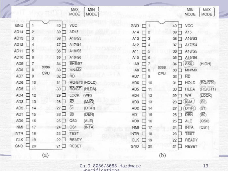
Fig. 9-1 : Pin-outs of 8086/808840-pin dual in-line packages(DIPs)
difference :data bus width → 8086 : 16 bit, 8088 : 8 bit
pin 28 → 8086 : M/IO’, 8088 : IO/M’
pin 34 → 8086 : BHE’/S7, 8088 : SS0

Ch.9 8086/8088 Hardware Specifications
3
Fig. 9-1Fig. 9-1
Ch.9 8086/8088 Hardware Specifications
4
9-1 Pin-outs and the pin functions
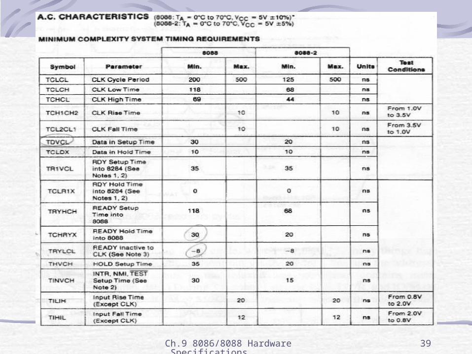
Power Supply Requirement : +5.0V 10%
maximum supply current : 360mA(8086), 340(8088)
operate in ambient temperature : 32ºF ~ 180ºF(0~82°C)
CMOS version : 80C86, 80C88(10mA, -40ºF ~ 225ºF(-40~ 107°C))
DC Characteristics :
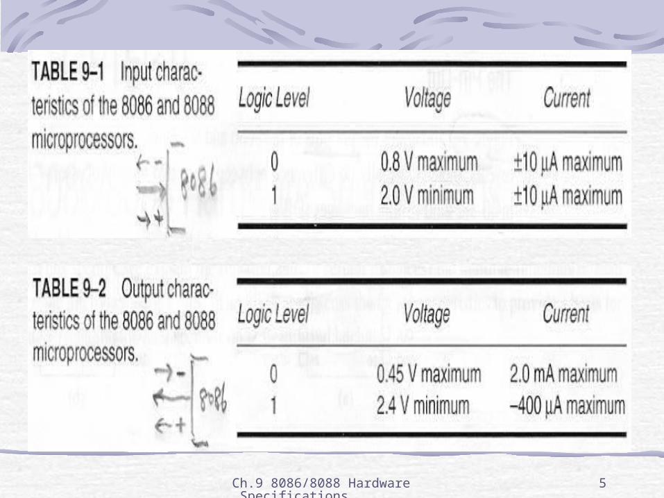
Input Characteristics : Table 9-1input current requirement for input pin
gates connections of MOSFETs and represent leakage current
Ch.9 8086/8088 Hardware Specifications
5
Table 9-1,2Table 9-1,2

Ch.9 8086/8088 Hardware Specifications
6
9-1 Pin-outs and the pin functionsOutput Characteristics : Table 9-2
output current drive capability for output pin
logic 1 voltage level : compatible most standard logic family
logic 0 voltage level : max. 0.45V(standard logic : max. 0.4V)
this difference : reduced noise immunity from standard level 0.4V(0.8-0.4) to 0.35V(0.8-0.45)
noise immunity : difference between logic 0 output voltage and logic 0 input voltage levels
reduced noise immunity may result in problems : long wire connection, too many load
recommended : no more than 10 loads without buffering
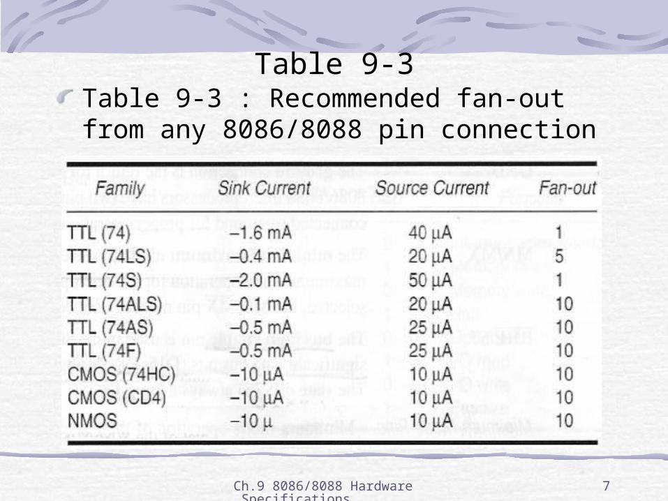
Table 9-3: best choice for connection to 8086→LS,ALS,HC
Ch.9 8086/8088 Hardware Specifications
7
Table 9-3Table 9-3 : Recommended fan-out from any 8086/8088 pin connection

Ch.9 8086/8088 Hardware Specifications
8
Pin Connections
AD7-AD0 : address/data bus(multiplexed)memory address or I/O port no : whenever ALE = 1
data : whenever ALE = 0
high-impedance state : during a hold acknowledge
A15-A8 : 8088 address bushigh-impedance state : during a hold acknowledge
AD15-AD8 : address/data bus(multiplexed)memory address bits A15-A8 : whenever ALE = 1
data bits D15-D8 : whenever ALE = 0
high-impedance state : during a hold acknowledge

Ch.9 8086/8088 Hardware Specifications
9
Pin ConnectionsA19/S6-A16/S3 : address/status bus(multiplexed)
memory address A19-A16, status bits S6-S3
high-impedance state : during a hold acknowledge
S6 : always remain a logic 0
S5 : indicate condition of IF flag bits
S4, S3 : show which segment is accessed during current bus cycle(Table 9-4)
S4, S3 : can used to address four separate 1M byte memory banks by decoding them as A21, A20
Ch.9 8086/8088 Hardware Specifications
10
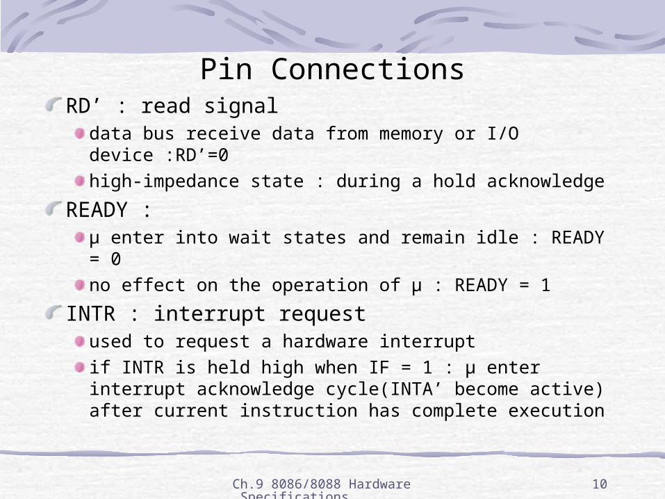
Pin ConnectionsRD’ : read signal
data bus receive data from memory or I/O device :RD’=0
high-impedance state : during a hold acknowledge
READY :µ enter into wait states and remain idle : READY = 0
no effect on the operation of µ : READY = 1
INTR : interrupt requestused to request a hardware interrupt
if INTR is held high when IF = 1 : µ enter interrupt acknowledge cycle(INTA’ become active) after current instruction has complete execution
Ch.9 8086/8088 Hardware Specifications
11
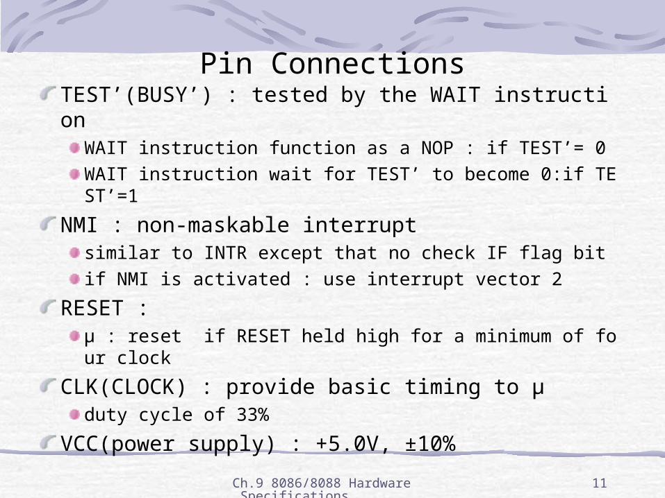
Pin ConnectionsTEST’(BUSY’) : tested by the WAIT instruction
WAIT instruction function as a NOP : if TEST’= 0
WAIT instruction wait for TEST’ to become 0:if TEST’=1
NMI : non-maskable interruptsimilar to INTR except that no check IF flag bit
if NMI is activated : use interrupt vector 2
RESET : µ : reset if RESET held high for a minimum of four clock
CLK(CLOCK) : provide basic timing to µduty cycle of 33%
VCC(power supply) : +5.0V, ±10%

Ch.9 8086/8088 Hardware Specifications
12
Pin ConnectionsGND(Ground) : two pins labeled GND
MN/MX’ : select either minimum or maximum mode
BHE’/S7 : bus high enable
enable the most significant data bus bits(D15-D8) during read or write operation
status of S7 : always a logic 1
Minimum Mode Pins: MN = 1(directly to +5.0V) next p
IO/M’(8088) or M/IO’(8086) : select memory or I/O
address bus : whether memory or I/O port address
WR’ : write signal(high impedance state during hold ack.)
strobe that indicate that output data to memory or I/O
during WR’=0 : data bus contains valid data for M or I/O
Ch.9 8086/8088 Hardware Specifications
13
Fig. 9-1Fig. 9-1

Ch.9 8086/8088 Hardware Specifications
14
Minimum Mode PinsINTA’(interrupt acknowledge) : response to INTR input pin
normally used to gate interrupt vector no onto data bus
ALE(address latch enable) : does not float during hold ack
address/data bus : contain address information
DT/R’(data transmit/receive) :
data bus : transmit(DT/R’=1) or receive(DT/R’=0) data
used to enable external data bus buffers
DEN(data bus enable) : activate external data bus buffers
HOLD : request a direct memory access(DMA)if HOLD=1 : µ stops executing software and places address, data, and control bus at high-impedance state
HOLD=0 : µ execute software normally
Ch.9 8086/8088 Hardware Specifications
15
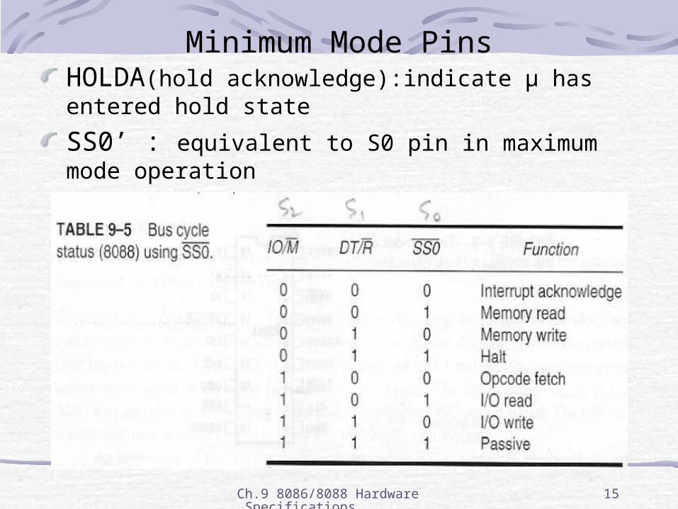
Minimum Mode PinsHOLDA(hold acknowledge):indicate µ has entered hold state
SS0’ : equivalent to S0 pin in maximum mode operation
combined with IO/M’, DT/R’ to decode function of current bus cycle(Table 9-5)

Ch.9 8086/8088 Hardware Specifications
16
Maximum Mode PinsMN/MX’ = 0(ground) next page
S2’,S1’,S0’:indicate function of current bus cycle(T 9-6)
these signal : normally decoded by 8288 bus controller

Ch.9 8086/8088 Hardware Specifications
17
Fig. 9-1Fig. 9-1
Ch.9 8086/8088 Hardware Specifications
18
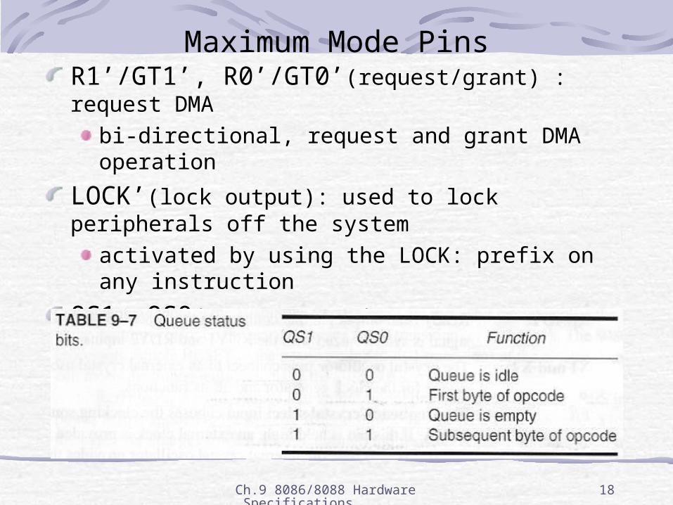
Maximum Mode PinsR1’/GT1’, R0’/GT0’(request/grant) : request DMA
bi-directional, request and grant DMA operation
LOCK’(lock output): used to lock peripherals off the system
activated by using the LOCK: prefix on any instruction
QS1, QS0(queue status) :
show status of internal instruction queue : Table 9-7
provided for access by the numeric coprocessor(8087)
Ch.9 8086/8088 Hardware Specifications
19
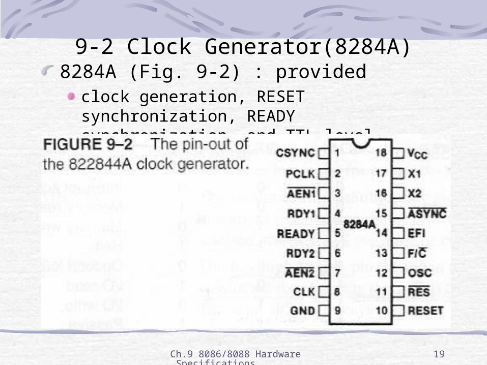
9-2 Clock Generator(8284A)8284A (Fig. 9-2) : provided
clock generation, RESET synchronization, READY synchronization, and TTL-level peripheral clock signal

Ch.9 8086/8088 Hardware Specifications
20
8284A Pin FunctionsAEN1’, AEN2’(address enable) : provided
to qualify bus ready signal RDY1, RDY2
RDY1, RDY2(bus ready) : provided, in conjunction with AEN1’,AEN2’ pins, to cause wait states
ASYNC’(ready synchronization) selection input: select either
one or two stages of synchronization for RDY1,RDY2
READY: output pin that connects to 8086/88 READY input
X1, X2(crystal oscillator) : connect to external crystal
used as timing source for clock generator
F/C’(frequency/crystal) input : choose clocking sourceF/C’=1 : provided external clock to EFI input pin, F/C’=0 : internal crystal oscillator

Ch.9 8086/8088 Hardware Specifications
21
8284A Pin FunctionsEFI(external frequency input) : supplied
the timing whenever F/C’ pin is pulled high
CLK(clock output) : provided CLK input to 8086/8088 and other components1/3 of crystal or EFI input frequency33% duty cycle which is required by 8086/8088
PCLK(peripheral clock) : provided peripheral
1/6 of crystal or EFI input frequency, 50% duty cycle
OSC(oscillator output) : TTL-level signal
same frequency as crystal or EFI input
RES’(reset input) : often connected
to RC network that provide power-on resetting
Ch.9 8086/8088 Hardware Specifications
22
8284A Pin FunctionsRESET output : connected to 8086/8088 RESET input
CSYNC(clock synchronization) : used whenever EFI provides synchronization in system with multiple processors
must be grounded, if internal crystal oscillator is used
GND(ground) : connected to ground
VCC(power supply) : +5.0V ±10%
Fig. 9-3 : internal block diagram of 8284Aclock section : middle part
reset section : top part
ready section : bottom part
Ch.9 8086/8088 Hardware Specifications
23
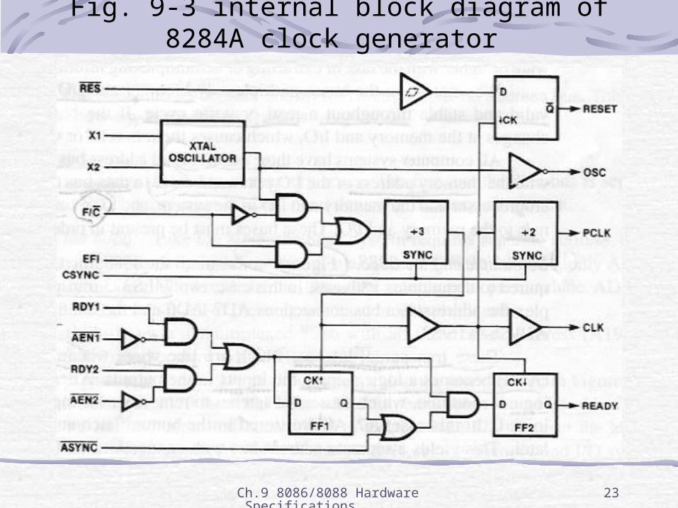
Fig. 9-3 internal block diagram of 8284A clock generator
Fig. 9-3
Ch.9 8086/8088 Hardware Specifications
24
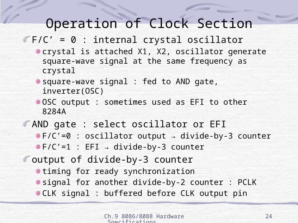
Operation of Clock SectionF/C’ = 0 : internal crystal oscillator
crystal is attached X1, X2, oscillator generate square-wave signal at the same frequency as crystal
square-wave signal : fed to AND gate, inverter(OSC)
OSC output : sometimes used as EFI to other 8284A
AND gate : select oscillator or EFIF/C’=0 : oscillator output → divide-by-3 counter
F/C’=1 : EFI → divide-by-3 counter
output of divide-by-3 countertiming for ready synchronization
signal for another divide-by-2 counter : PCLK
CLK signal : buffered before CLK output pin

Ch.9 8086/8088 Hardware Specifications
25
Operation of the Reset Section
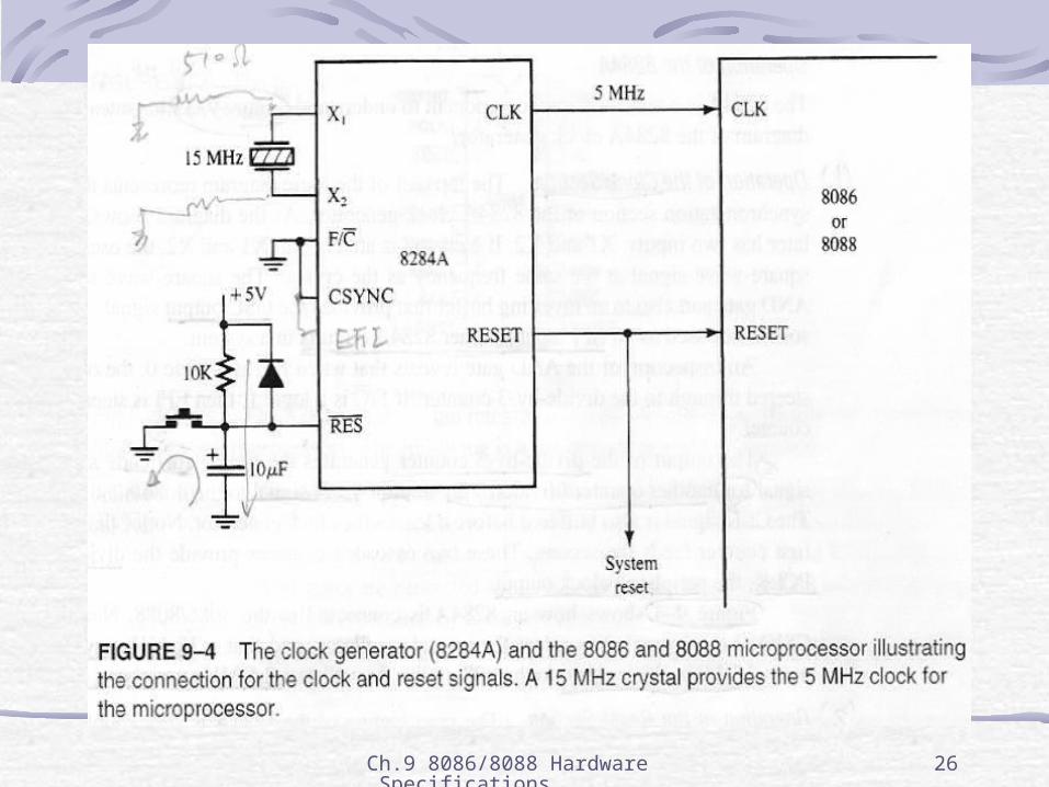
Fig. 9-4 : crystal oscillator(F/C’=CSYNC=0)15MHz crystal : 5MHz clock signal, 2.5MHz PCLK
Reset : a Schmitt trigger buffer, a D-type FFD FF : ensured timing requirements of 8086 RESET
applied RESET signal to µ on negative edge of each clock
8086 µ : sampled RESET at positive edge of clocks
1. power on reset, 2. reset button
µ RESET : to become logic 1 no later than 4 clocks after power is applied, (FF make certain that RESET goes high in4 clock)
and to be held high for at least 50 ㎲ (RC time constant)
Ch.9 8086/8088 Hardware Specifications
26
Fig. 9-4Fig. 9-4
Ch.9 8086/8088 Hardware Specifications
27
9-3 Bus Buffering and LatchingDemultiplexing the Buses
address/data bus:multiplexed(shared) to reduce no of pins
memory and I/O : require that address remains valid and stable throughout a read and write cycle
all computer systems : have three busesaddress bus : provided memory and I/O with memory address or I/O port number
data bus : transferred data between µ and memory or I/O
control bus : provided control signal to memory and I/O
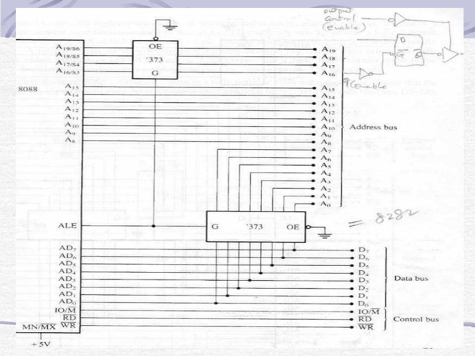
Demultiplexing the 8088 : Fig. 9-5two 74LS373 transparent latches :
pass inputs to outputs whenever ALE become 1
after ALE return 0, remember inputs at time of change to 0
28
Fig. 9-5Fig. 9-5
Ch.9 8086/8088 Hardware Specifications
29
9-3 Bus Buffering and Latching
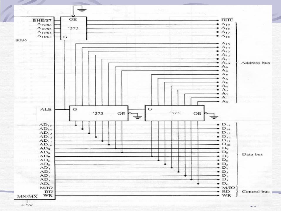
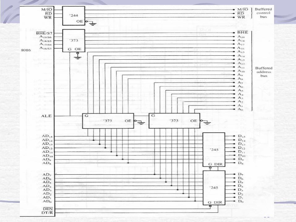
Demultiplexing the 8086 : Fig. 9-6demultiplexing: AD15-AD0, A19/S6-A16/S3, BHE’/S3
3 buses : address(A19-A0, BHE’), data(D15-D0), control(M/IO’, RD’,WR’)
three 74LS373 transparent latches
The Buffered Systemµ system must be buffered : if more than 10 unit load are attached to any bus pin
demultiplexed pins : already buffered by 74LS373 latch
buffer’s output currents increased : 32mA of sink current(0), 5.2mA of source current(1)
30
Fig. 9-6Fig. 9-6
Ch.9 8086/8088 Hardware Specifications
31
9-3 Bus Buffering and Latching
fully buffered signal : will introduce timing delay
cause no difficulty : unless memory and I/O devices are used, which function at near maximum speed of bus
The fully Buffered 8088 : Fig. 9-78 address A15-A8 : 74LS244 octal buffer
IO/M’, RD’, WR’ : 74LS244
8 data D7-D0 : 74LS245 octal bi-directional bus buffer
direction : controlled by DT/R’, enable : by DEN’
The fully Buffered 8086 : Fig. 9-8data bus : two 74LS245
IO/M’, RD’, WR’ : 74LS244

32
Fig. 9-7Fig. 9-7
33
Fig. 9-8Fig. 9-8
Ch.9 8086/8088 Hardware Specifications
34
9-4 Bus Timing
Basic Bus Operation
if data are written : Fig. 9-9(address, data, WR’ & M/IO’)
if data are read : Fig. 9-10(address, RD’ & M/IO’)
Timing in General
bus cycle : 8086/8088 µ use memory & I/O in periods called bus cycles
equal 4 (or as few as 2) system-clocking periods(T states)
800ns : 5MHz basic operating frequency
read or write at maximum rate of 1.25 million times a sec.
because internal queue, µ execute 2.5 MIPS in bursts

35
Fig. 9-9,10Fig. 9-9,10
Ch.9 8086/8088 Hardware Specifications
36
Timing in GeneralT1 : 1st clocking period
address of memory or I/O : sent out via address bus
control signal ALE, DT/R’, M/IO’(IO/M’) : output
T2 : issue RD’ or WR’, DEN’
in case of write : data to be written appear on data bus
READY : sampled at the end of T2(Fig. 9-11)if READY is low at end of T2 : T3 becomes a wait state(Tw)
if read bus cycle : data bus is sampled at end of T3
T4 :all bus signals : deactivated in preparation for next bus cycle
µ sampled data bus for data that read from M or I/O
trailing edge of WR’ : transfer data to memory or I/O

Ch.9 8086/8088 Hardware Specifications
37
Fig. 9-11Fig. 9-11

Ch.9 8086/8088 Hardware Specifications
38
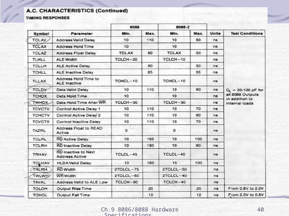
Read TimingFig. 9-11 : depict read timing for 8088/8086
fixed amount of time allowed memory or I/O to read dataat end of T3 : µ sample the data bus
address access time: TAVDV = 3TCLCL - TCLAV - TDVCL = 3200–110–30=460 ns
TCLAV : time that appeared address on address bus
TDVCL : data setup time
time delay(30-40ns) : address decoders and buffersmemory speed : no slower than about 420ns
read access time :TRLDV = 2TCLCL - TCLRL - TDVCL = 2200–165–30=205 ns
width of RD’ strobe :TRLRH = 2TCLCL – 75ns = 2 200 – 75 = 325 ns
Ch.9 8086/8088 Hardware Specifications
39
Fig. 9-12Fig. 9-12
Ch.9 8086/8088 Hardware Specifications
40
Fig. 9-12(continued)Fig. 9-12
Ch.9 8086/8088 Hardware Specifications
41
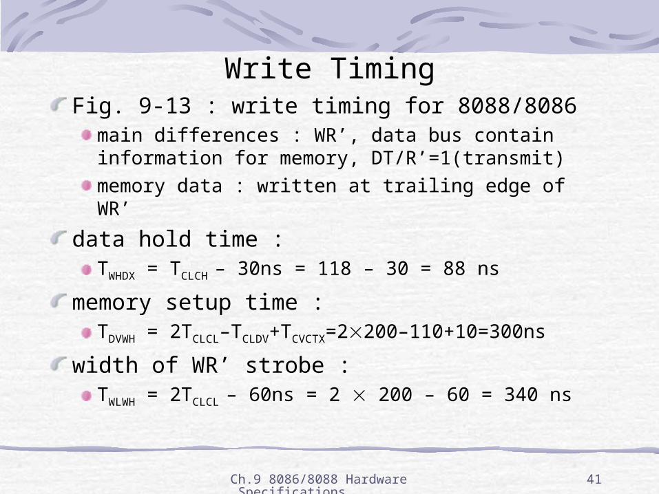
Write TimingFig. 9-13 : write timing for 8088/8086
main differences : WR’, data bus contain information for memory, DT/R’=1(transmit)
memory data : written at trailing edge of WR’
data hold time :TWHDX = TCLCH – 30ns = 118 – 30 = 88 ns
memory setup time : TDVWH = 2TCLCL–TCLDV+TCVCTX=2200–110+10=300ns
width of WR’ strobe :TWLWH = 2TCLCL – 60ns = 2 200 – 60 = 340 ns

42
Fig. 9-13Fig. 9-13

Ch.9 8086/8088 Hardware Specifications
43
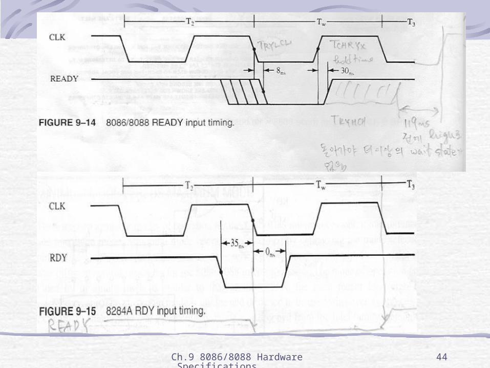
9-5 Ready and the Wait Statewait state(TW) :
an extra clocking period, inserted between T2 & T3
READY input : cause wait states for slower memory & I/O components
sampled at the end of T2, if applicable, in middle of TW
if READY = 0 at end of T2 : T3 is delayed and TW is inserted between T2 and T3
READY is next sampled at middle of TW : to determine whether the next state is TW or T3
timing diagram : Fig. 9-14(Fig. 9-11)required setup and hold time from system clock
met by internal READY synchronization circuit of 8284A
Ch.9 8086/8088 Hardware Specifications
44
Fig. 9-14, 15Fig. 9-14, 15
Ch.9 8086/8088 Hardware Specifications
45
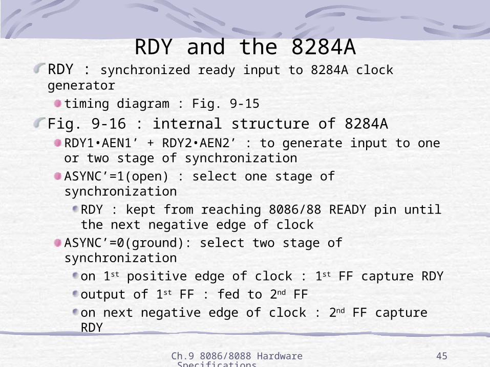
RDY and the 8284ARDY : synchronized ready input to 8284A clock generator
timing diagram : Fig. 9-15
Fig. 9-16 : internal structure of 8284ARDY1•AEN1’ + RDY2•AEN2’ : to generate input to one or two stage of synchronization
ASYNC’=1(open) : select one stage of synchronization
RDY : kept from reaching 8086/88 READY pin until the next negative edge of clock
ASYNC’=0(ground): select two stage of synchronization
on 1st positive edge of clock : 1st FF capture RDY
output of 1st FF : fed to 2nd FF
on next negative edge of clock : 2nd FF capture RDY

Ch.9 8086/8088 Hardware Specifications
46
Fig. 9-16Fig. 9-16

Ch.9 8086/8088 Hardware Specifications
47
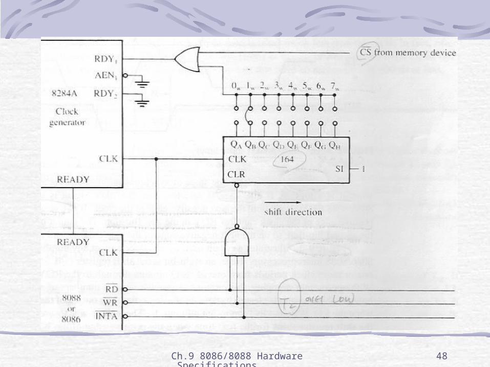
RDY and the 8284AFig. 9-17, 18 :
circuit that generated almost any no of wait states for µ
8-bit shift reg.(74LS164) : shift 0 for one or more clock periods from one of its Q outputs through to RDY1
cleared back to its starting point
RD’=WR’=INTA’=1 : until state T2 → Q = 0
positive edge of T2 : shift right, QA = 1(because SI=1)
RDY1 = 0 : CS’ = 0 or QB = 0
inserted wait cycle
positive edge of TW : shift right, QA = QB = 1
RDY1 = 1 : CS’ = 0 or QB = 1
no more inserted wait cycle
Ch.9 8086/8088 Hardware Specifications
48
Fig. 9-17Fig. 9-17
Ch.9 8086/8088 Hardware Specifications
49
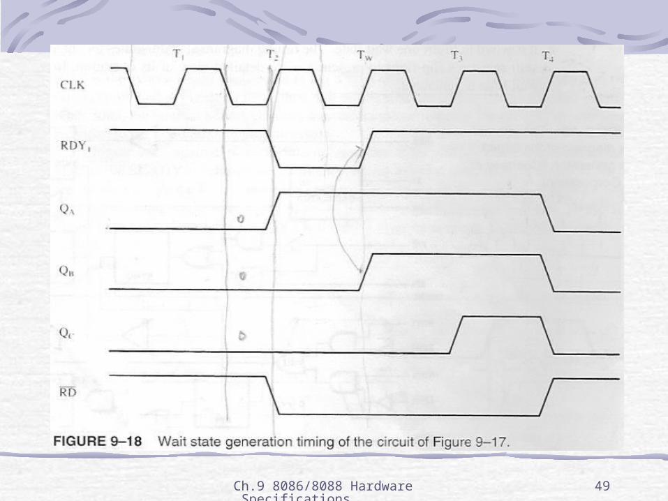
Fig. 9-18Fig. 9-18
Ch.9 8086/8088 Hardware Specifications
50
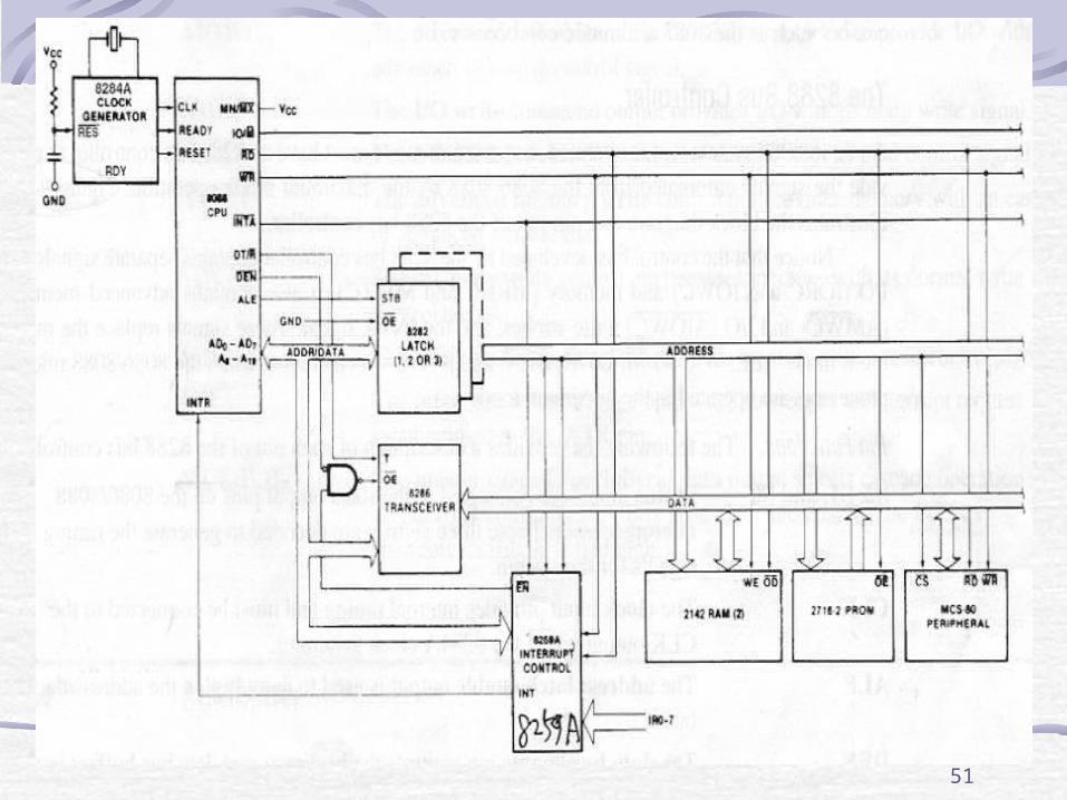
9-6 Minimum Mode versus Maximum Mode
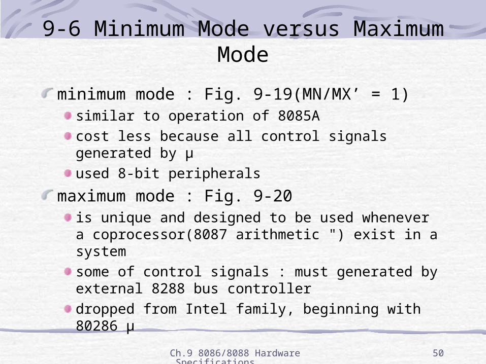
minimum mode : Fig. 9-19(MN/MX’ = 1)similar to operation of 8085A
cost less because all control signals generated by µ
used 8-bit peripherals
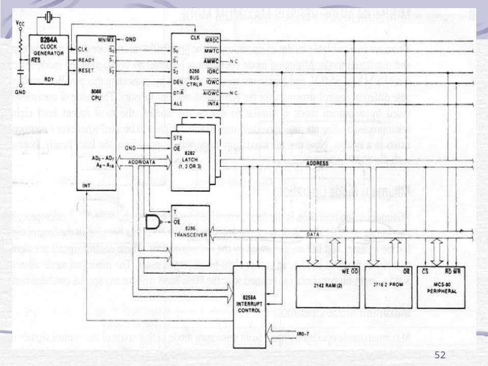
maximum mode : Fig. 9-20is unique and designed to be used whenever a coprocessor(8087 arithmetic ") exist in a system
some of control signals : must generated by external 8288 bus controller
dropped from Intel family, beginning with 80286 µ
51
Fig. 9-19Fig. 9-19
52
Fig. 9-20Fig. 9-20

Ch.9 8086/8088 Hardware Specifications
53
The 8288 Bus Controller8288 : Fig. 9-21
provided signals eliminated from 8086/88 by maximum mode operation
S2,S1,S0 (status) input : connected to status output on µ
devoted to generate the timing signals for the system
CLK input : connected CLK output of 8284A
provided internal timing
ALE(address latch enable) output : used to demultiplex the address/data bus
DEN(data bus enable) output : control bi-directional data bus buffers
DT/R’(data transmit/receive) output : "

54
Fig. 9-21Fig. 9-21
Ch.9 8086/8088 Hardware Specifications
55
The 8288 Bus ControllerAEN’(address enable) input : cause to enable memory control signals
CEN(control enable) input: enable the command output
IOB(I/O bus mode) input : select either system bus or I/O bus mode mode operation
AIOWC’(advanced I/O write command) output : provide I/O with its advanced I/O write control signal
IOWC’(I/O write) : provide I/O with its main write signal
IORC’, AMWC’, MWTC’, MRDC’
INTA’(interrupt acknowledge) output :
MCE/PDEN’(master cascade/peripheral data) output : select cascade operation for interrupt controller if IOB is 0, and enable the I/O bus transceivers if I/O is 1
Related Documents


![Week 8 The 8088 and 8086 Microprocessorsalkar/ELE336/w7-hacettepe[2016].pdf · 8086 and 8088 Microprocessors • 8086 announced in 1978; 8086 is a 16 bit ... –Widely used is the](https://static.cupdf.com/doc/110x72/5a7657cc7f8b9a1b688d2257/week-8-the-8088-and-8086-microprocessors-alkarele336w7-hacettepe2016pdf.jpg)