Chapter 7 – Registers and Chapter 7 Registers and Register Transfers Part 2 – Counters, Register Cells, Buses, & Serial Operations Logic and Computer Design Fundamentals Efth l CK i (PhD) A i P f Efthyvoulos C. Kyriacou (PhD) Assis. Prof. Computer Science and Engineering Department Frederick University Sources: Charles Kime & Thomas Kaminski © 2004 Pearson Education, Inc. Terms of Use (Hyperlinks are active in View Show mode)

Welcome message from author
This document is posted to help you gain knowledge. Please leave a comment to let me know what you think about it! Share it to your friends and learn new things together.
Transcript
Chapter 7 – Registers andChapter 7 Registers and Register Transfers
Part 2 – Counters, Register Cells, Buses, & Serial Operations
Logic and Computer Design FundamentalsEfth l C K i (PhD) A i P fEfthyvoulos C. Kyriacou (PhD) Assis. Prof.
Computer Science and Engineering Department
Frederick University
Sources: Charles Kime & Thomas Kaminski
© 2004 Pearson Education, Inc.,Terms of Use
(Hyperlinks are active in View Show mode)
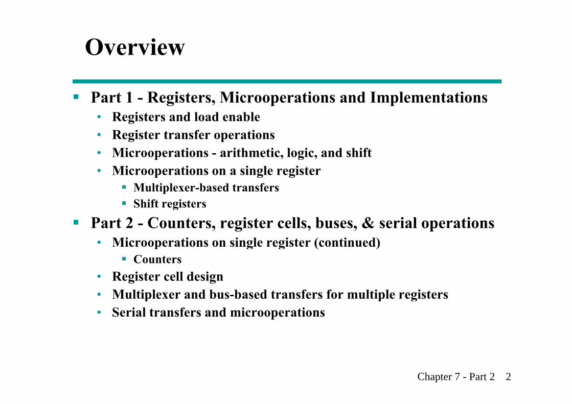
Overview
Part 1 - Registers, Microoperations and Implementations• Registers and load enable• Register transfer operations• Microoperations - arithmetic, logic, and shiftMicrooperations arithmetic, logic, and shift• Microoperations on a single register
Multiplexer-based transfersShift registersShift registers
Part 2 - Counters, register cells, buses, & serial operations• Microoperations on single register (continued)p g g ( )
Counters• Register cell design• Multiplexer and bus based transfers for multiple registers• Multiplexer and bus-based transfers for multiple registers• Serial transfers and microoperations
Chapter 7 - Part 2 2

Counters
Counters are sequential circuits which "count" through ifia specific state sequence. They can count up, count
down, or count through other fixed sequences. Two distinct types are in common usage:distinct types are in common usage:Ripple Counters
• Clock is connected to the flip-flop clock input on the LSB bitClock is connected to the flip flop clock input on the LSB bit flip-flop
• For all other bits, a flip-flop output is connected to the clock i t th i it i t t l hinput, thus circuit is not truly synchronous
• Output change is delayed more for each bit toward the MSB.• Resurgent because of low power consumptionResurgent because of low power consumption
Synchronous Counters• Clock is directly connected to the flip-flop clock inputs
Chapter 7 - Part 2 3
y p p p• Logic is used to implement the desired state sequencing

Ripple Counter
How does it work? D A• When there is a positive
edge on the clock inputClock
D
CR
A
of A, A complements• The clock input for flip-
fl B i th l t dD B
flop B is the complementedoutput of flip-flop A
• When flip A changes
ResetCR
• When flip A changesfrom 1 to 0, there is apositive edge on the
CP
positive edge on theclock input of Bcausing B to B
A
Chapter 7 - Part 2 4
complement0 1 2 3 0 1
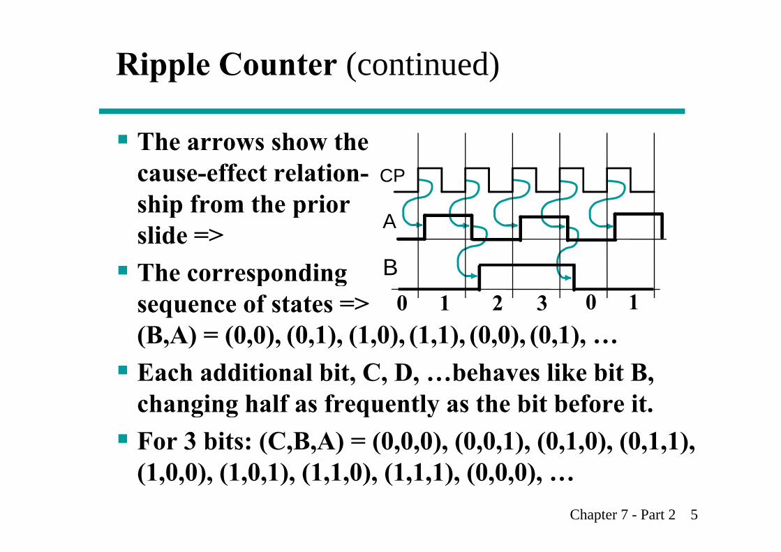
Ripple Counter (continued)
The arrows show thecause-effect relation-ship from the prior
CPp p
slide =>The corresponding B
A
The correspondingsequence of states =>(B A) = (0 0) (1 0)(0 1) (0 1)(0 0)(1 1)
0 1 2 3 0 1(B,A) (0,0),Each additional bit, C, D, …behaves like bit B, changing half as frequently as the bit before it
(1,0),(0,1), (0,1), …(0,0),(1,1),
changing half as frequently as the bit before it.For 3 bits: (C,B,A) = (0,0,0), (0,0,1), (0,1,0), (0,1,1),(1 0 0) (1 0 1) (1 1 0) (1 1 1) (0 0 0)
Chapter 7 - Part 2 5
(1,0,0), (1,0,1), (1,1,0), (1,1,1), (0,0,0), …
Ripple Counter (continued)
These circuits are called ripple counters because ppeach edge sensitive transition (positive in the example) causes a change in the next flip-flop’s p ) g p pstate.The changes “ripple” upward through theThe changes ripple upward through the chain of flip-flops, i. e., each transition occurs after a clock-to-output delay from the stageafter a clock to output delay from the stage before.To see this effect in detail look at the waveformsTo see this effect in detail look at the waveforms on the next slide.
Chapter 7 - Part 2 6
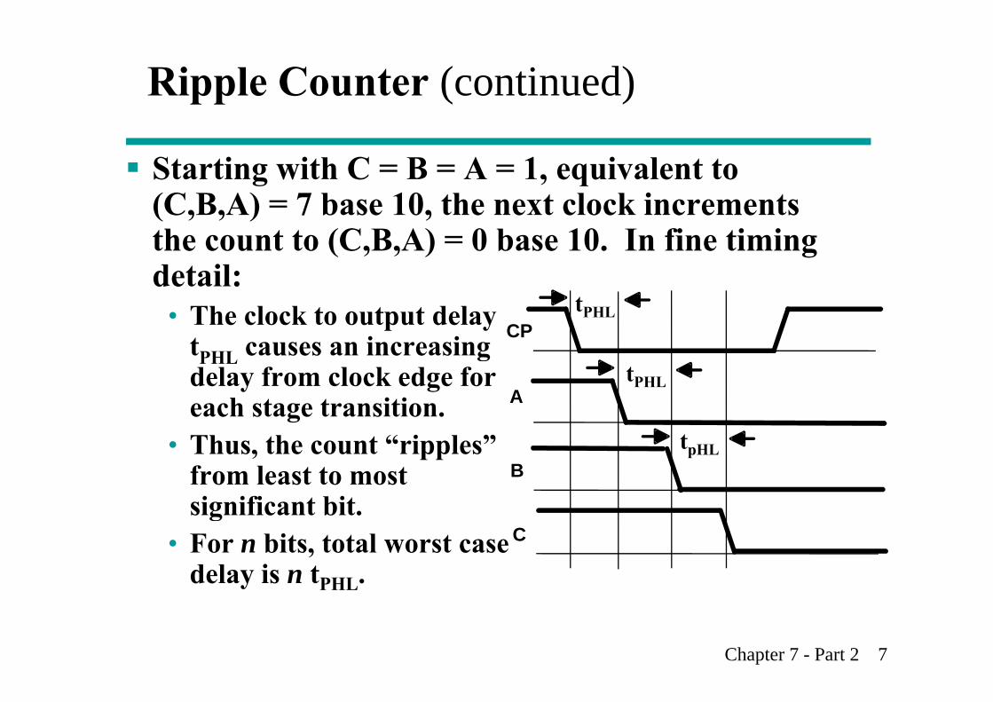
Ripple Counter (continued)
Starting with C = B = A = 1, equivalent to (C,B,A) = 7 base 10, the next clock increments the count to (C,B,A) = 0 base 10. In fine timing detail:detail:
• The clock to output delayt causes an increasing CP
tPHL
tPHL causes an increasingdelay from clock edge foreach stage transition. A
tPHL
• Thus, the count “ripples”from least to mostsignificant bit
BtpHL
significant bit.• For n bits, total worst case
delay is n tPHL.C
Chapter 7 - Part 2 7
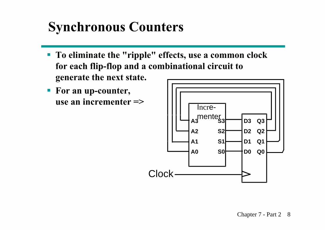
Synchronous Counters
To eliminate the "ripple" effects, use a common clock f f i f i i i ifor each flip-flop and a combinational circuit to generate the next state.F tFor an up-counter,use an incrementer => Incre-
menter D3 Q3
D2 Q2
D1 Q1
menterA3
A2
A1
S3
S2
S1 D1 Q1
D0 Q0
A1
A0
S1
S0
Clock
Chapter 7 - Part 2 8

Synchronous Counters (continued)
Internal details => IncrementerD Q0Internal Logic
• XOR complements each bitAND h i l t
DC
Count enable EN Q0
• AND chain causes complementof a bit if all bits toward LSBfrom it equal 1
D
CQ1
Count Enable• Forces all outputs of AND
h i t 0 t “h ld” th t tD
CQ2
chain to 0 to “hold” the state
Carry Out• Added as part of incrementer
C
D Q3• Added as part of incrementer• Connect to Count Enable of
additional 4-bit counters to
DC
Carryt t CO
Q3
.
Chapter 7 - Part 2 9
form larger counters(a) Logic Diagram-Serial Gating
Clockoutput CO
Synchronous Counters (continued)
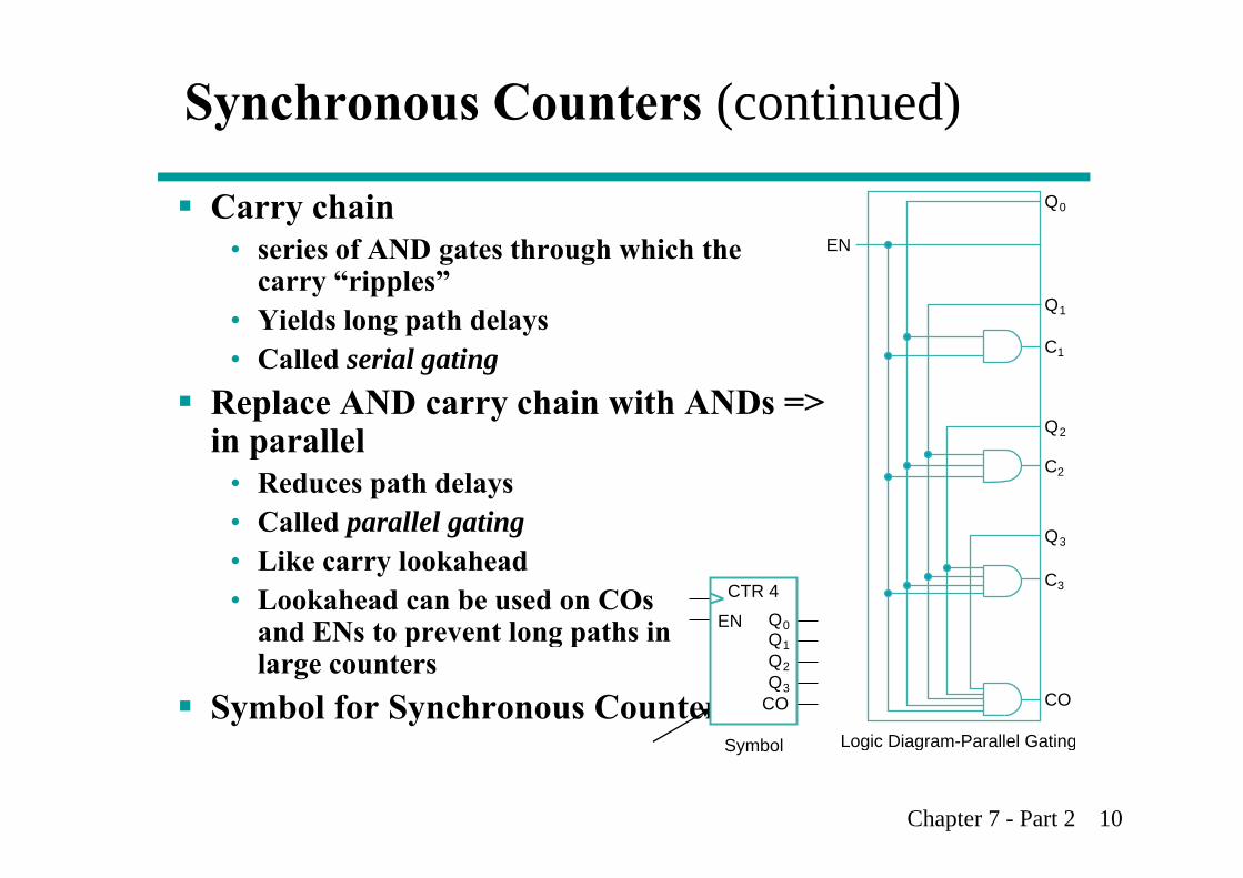
Carry chaini f AND h h hi h h EN
Q0
• series of AND gates through which thecarry “ripples”
• Yields long path delays
EN
Q1
• Called serial gatingReplace AND carry chain with ANDs =>in parallel
C1
Q2in parallel• Reduces path delays• Called parallel gating
C2
Q3
• Like carry lookahead• Lookahead can be used on COs
and ENs to prevent long paths inCTR 4
ENQQ0
C3
Q3
and ENs to prevent long paths inlarge counters
Symbol for Synchronous Counter
Q1Q2Q3
CO
Logic Diagram Parallel Gating
CO
Chapter 7 - Part 2 10
Symbol Logic Diagram-Parallel Gating
Other Counters
See text for:• Down Counter - counts downward instead of upward
• Up-Down Counter - counts up or down depending on valueUp Down Counter counts up or down depending on value a control input such as Up/Down
• Parallel Load Counter - Has parallel load of values available depending on control input such as Load
Divide-by-n (Modulo n) Counter• Count is remainder of division by n which n may not
be a power of 2 or• Count is arbitrary sequence of n states specifically
designed state-by-stateI l d d l 10 hi h i h BCD
Chapter 7 - Part 2 11
• Includes modulo 10 which is the BCD counter
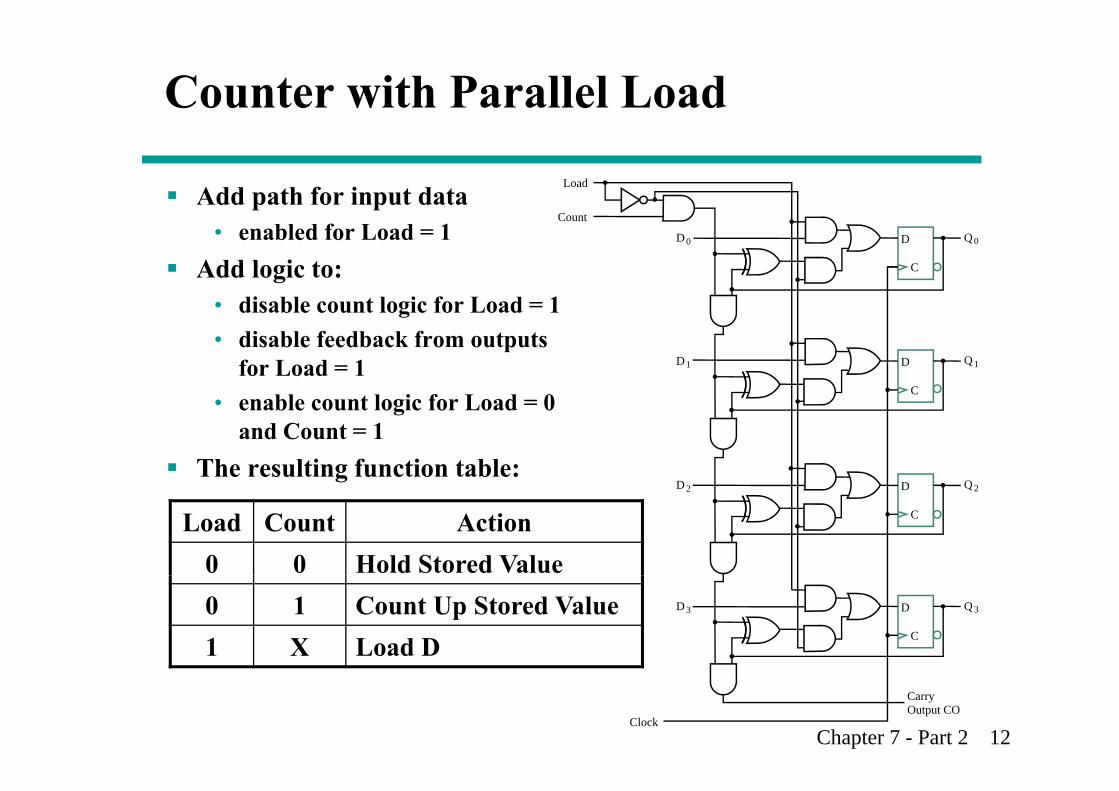
Counter with Parallel Load
Add path for input dataLoad
Count• enabled for Load = 1
Add logic to:• disable count logic for Load = 1
D 0 D
C
Q 0
Count
• disable count logic for Load = 1• disable feedback from outputs
for Load = 1bl t l i f L d 0
D 1 D
C
Q 1
• enable count logic for Load = 0and Count = 1
The resulting function table:D 2 D Q 2D 2 D
C
Q 2
Load Count Action0 0 Hold Stored Value
D 3 D
C
Q 30 1 Count Up Stored Value1 X Load D
Chapter 7 - Part 2 12Clock
CarryOutput CO
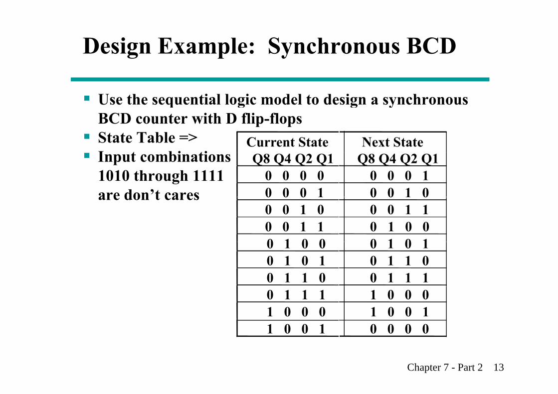
Design Example: Synchronous BCD
Use the sequential logic model to design a synchronous q g g yBCD counter with D flip-flopsState Table =>I t bi ti
Current State Next StateInput combinations1010 through 1111are don’t cares
Q8 Q4 Q2 Q1 Q8 Q4 Q2 Q10 0 0 0 0 0 0 10 0 0 1 0 0 1 0are don t cares 0 0 0 1 0 0 1 00 0 1 0 0 0 1 10 0 1 1 0 1 0 00 1 0 0 0 1 0 10 1 0 0 0 1 0 10 1 0 1 0 1 1 00 1 1 0 0 1 1 10 1 1 1 1 0 0 01 0 0 0 1 0 0 11 0 0 1 0 0 0 0
Chapter 7 - Part 2 13
1 0 0 1 0 0 0 0
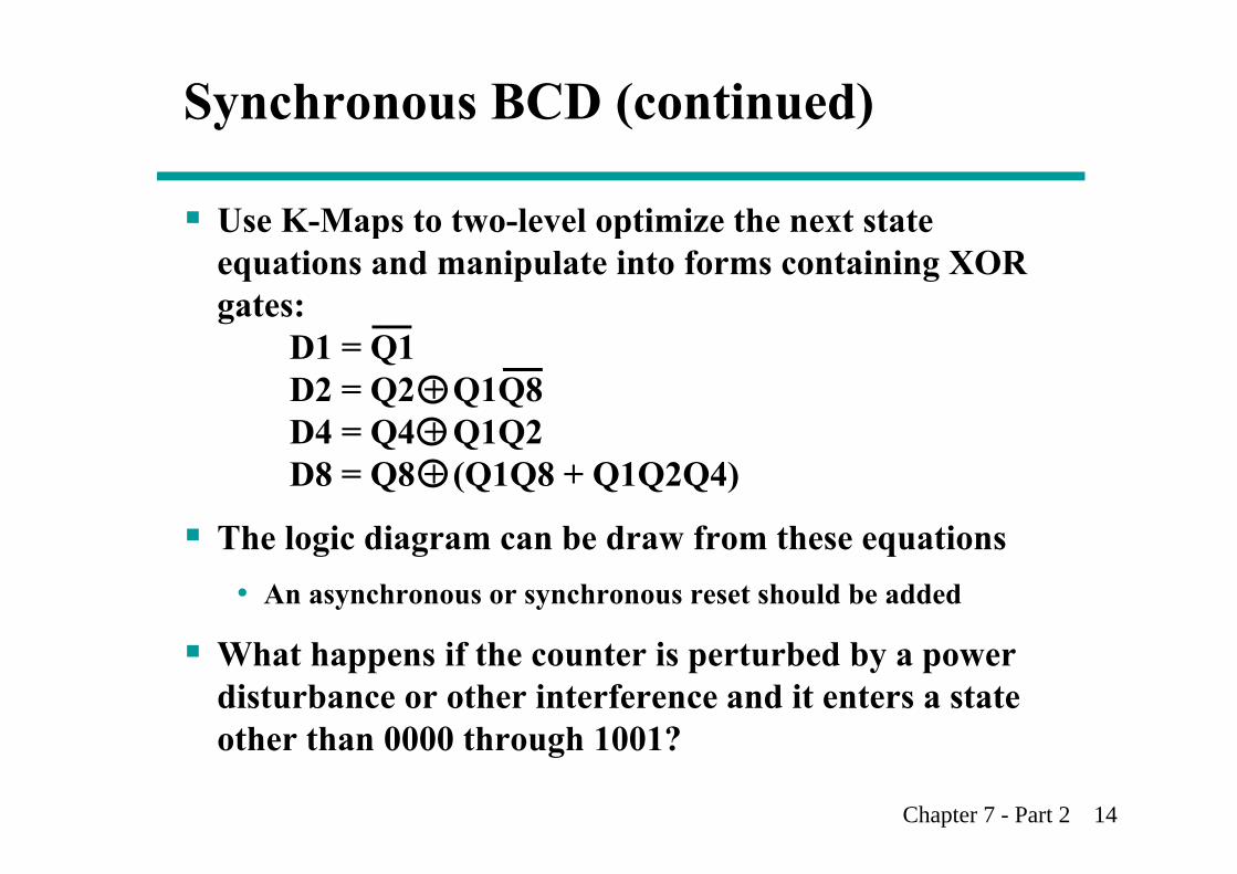
Synchronous BCD (continued)
Use K-Maps to two-level optimize the next state p pequations and manipulate into forms containing XOR gates:
D1 Q1D1 = Q1D2 = Q2 + Q1Q8D4 = Q4 + Q1Q2D4 Q4 + Q1Q2D8 = Q8 + (Q1Q8 + Q1Q2Q4)
The logic diagram can be draw from these equationsThe logic diagram can be draw from these equations• An asynchronous or synchronous reset should be added
What happens if the counter is perturbed by a power disturbance or other interference and it enters a state other than 0000 through 1001?
Chapter 7 - Part 2 14
other than 0000 through 1001?
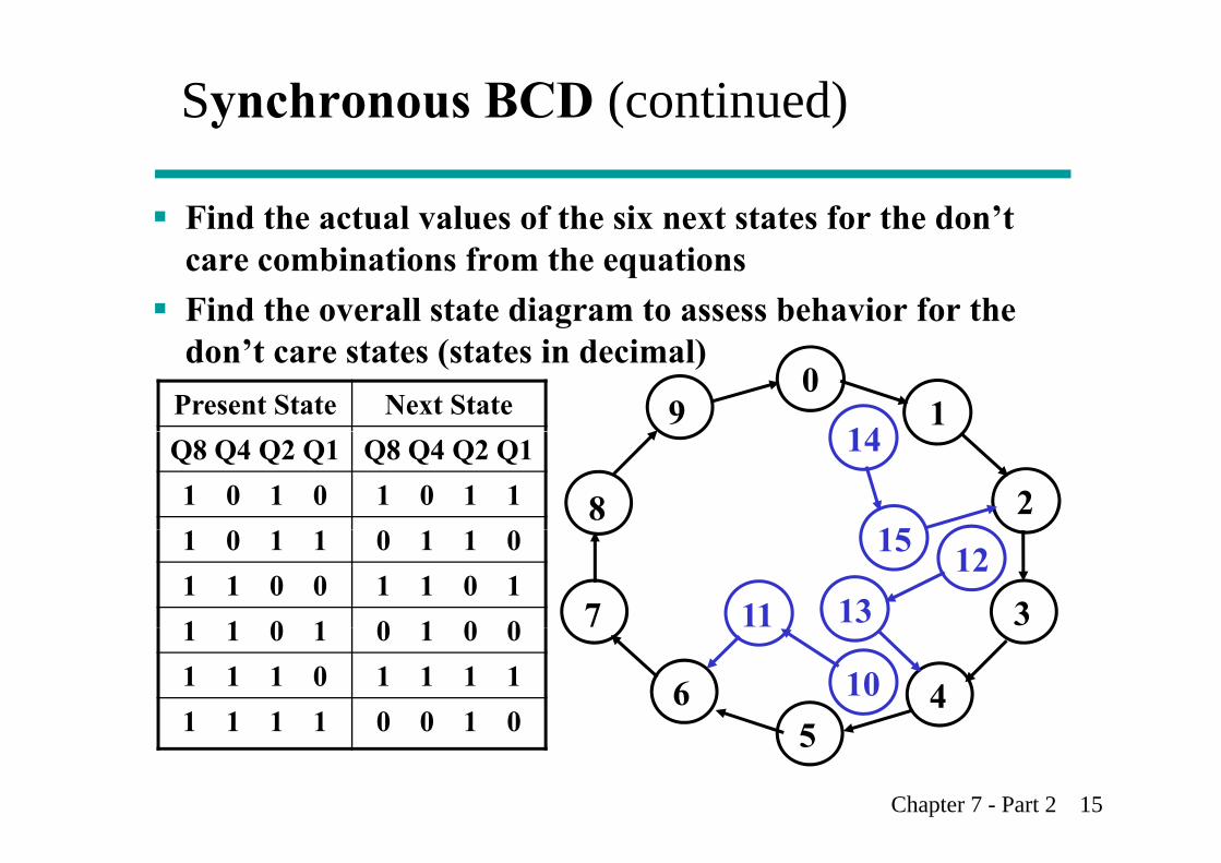
Synchronous BCD (continued)
Find the actual values of the six next states for the don’t care combinations from the equationsFind the overall state diagram to assess behavior for the don’t care states (states in decimal)
Present State Next State0
1914Q8 Q4 Q2 Q1 Q8 Q4 Q2 Q1
1 0 1 0 1 0 1 1 8 2
14
151 0 1 1 0 1 1 01 1 0 0 1 1 0 11 1 0 1 0 1 0 0 7 311
15 12131 1 0 1 0 1 0 0
1 1 1 0 1 1 1 11 1 1 1 0 0 1 0
65
410
Chapter 7 - Part 2 15
1 1 1 1 0 0 1 0 5

Synchronous BCD (continued)
For the BCD counter design, if an invalid state is entered, return to a valid state occurs within two clock cyclesI thi d t ? If tIs this adequate? If not:
• Is a signal needed that indicates that an invalid state has been entered? What is the equation for such a signal?entered? What is the equation for such a signal?
• Does the design need to be modified to return from an invalid state to a valid state in one clock cycle?
• Does the design need to be modified to return from a invalid state to a specific state (such as 0)?
The action to be taken depends on:The action to be taken depends on:• the application of the circuit• design group policy
Chapter 7 - Part 2 16
See pages 278 - 279 of the text.
Counting Modulo N
The following techniques use an n-bit binary counter with asynchronous or synchronous clear and/or parallel load:
• Detect a terminal count of N in a Modulo-N count sequence to asynchronously Clear the count to 0 or asynchronously Load inasynchronously Clear the count to 0 or asynchronously Load in value 0 (These lead to counts which are present for only a very short time and can fail to work for some timing conditions!)D i l f N 1 i M d l N• Detect a terminal count of N - 1 in a Modulo-N count sequence to Clear the count synchronously to 0
• Detect a terminal count of N - 1 in a Modulo-N count sequence to qsynchronously Load in value 0
• Detect a terminal count and use Load to preset a count of the terminal count value minus (N 1)terminal count value minus (N - 1)
Alternatively, custom design a modulo N counter as done for BCD
Chapter 7 - Part 2 17
BCD

Counting Modulo 7: Detect 7 and Asynchronously Clear
A synchronous 4-bit binary counter
Asynchronously Clear
y ywith an asynchronous Clear isused to make a Modulo7 t
D3 Q3
D2 Q27 counter. Use the Clear feature todetect the count 7 and
D1 Q1
D0 Q0detect the count 7 andclear the count to 0. Thisgives a count of 0, 1, 2, 3, 4,
Clock0
CLEAR
CPLOAD
gives a count of 0, 1, 2, 3, 4,5, 6, 7(short)0, 1, 2, 3, 4, 5,6, 7(short)0, etc.
CLEAR
DON’T DO THIS! Referred to as a “suicide” counter! (Count “7” is “killed,” but the designer’s job may be d d ll!)
Chapter 7 - Part 2 18
dead as well!)

Counting Modulo 7: Synchronously Load on Terminal Count of 6
A synchronous 4-bit binary
Terminal Count of 6
D3 Q30y ycounter with a synchronousload and an asynchronousl i d t k
D3 Q3
D2 Q2
D1 Q1
000
clear is used to make a Modulo 7 counter Use the Load feature to
Q
D0 Q0
CPClock
0
Use the Load feature todetect the count "6" andload in "zero". This gives
CLEARLOAD
Resetload in zero . This givesa count of 0, 1, 2, 3, 4, 5, 6,0, 1, 2, 3, 4, 5, 6, 0, ...Using don’t cares for statesabove 0110, detection of 6 can be done
ith L d Q4 Q2
Chapter 7 - Part 2 19
with Load = Q4 Q2
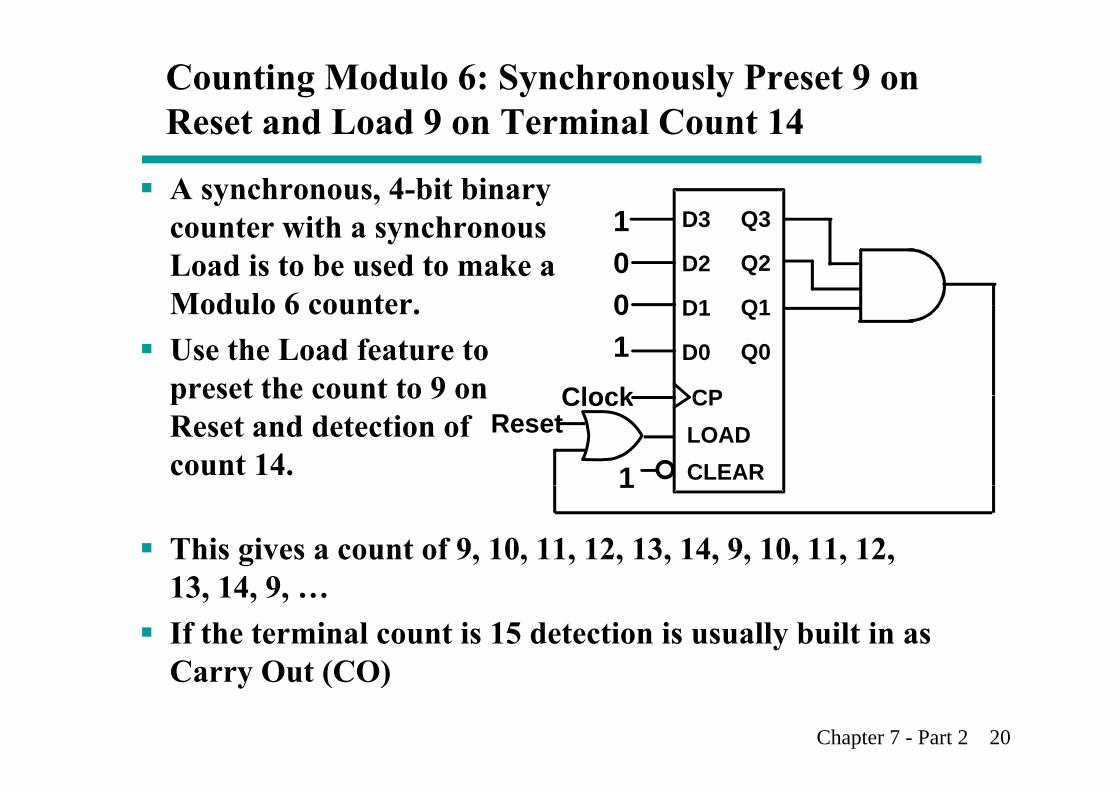
Counting Modulo 6: Synchronously Preset 9 on Reset and Load 9 on Terminal Count 14
A synchronous, 4-bit binaryi D3 Q31
Reset and Load 9 on Terminal Count 14
counter with a synchronousLoad is to be used to make aModulo 6 counter
D3 Q3
D2 Q2
D1 Q1
00
1
Modulo 6 counter. Use the Load feature topreset the count to 9 on Clock
D1 Q1
D0 Q0
CP
01
preset the count to 9 onReset and detection ofcount 14.
Clock
CLEAR
CPLOADReset
1
This gives a count of 9, 10, 11, 12, 13, 14, 9, 10, 11, 12,
1
13, 14, 9, …If the terminal count is 15 detection is usually built in as C O t (CO)
Chapter 7 - Part 2 20
Carry Out (CO)
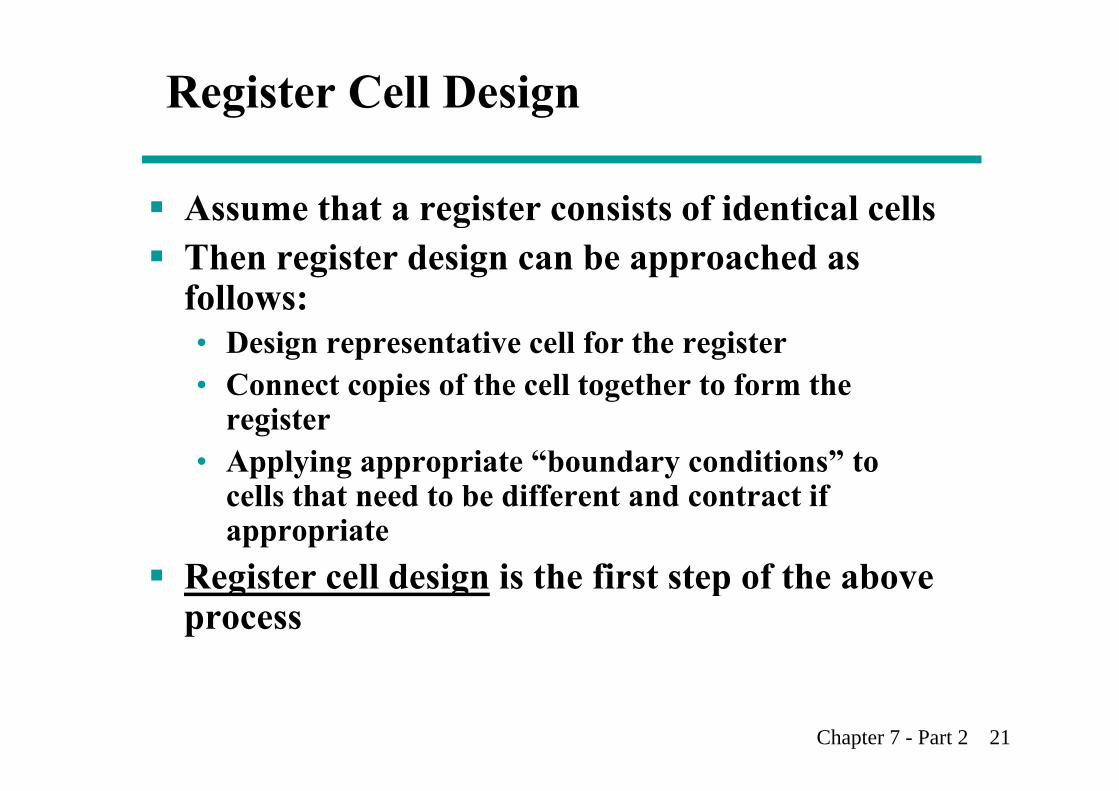
Register Cell Design
Assume that a register consists of identical cellsAssume that a register consists of identical cellsThen register design can be approached as follows:follows:• Design representative cell for the register • Connect copies of the cell together to form the p g
register• Applying appropriate “boundary conditions” to
ll h d b diff d ifcells that need to be different and contract if appropriate
Register cell design is the first step of the aboveRegister cell design is the first step of the above process
Chapter 7 - Part 2 21
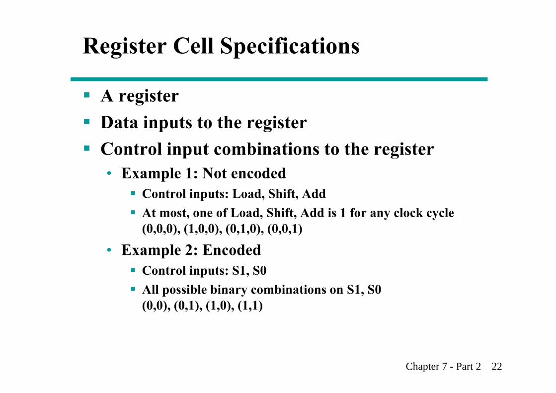
Register Cell Specifications
A registerData inputs to the registerControl input combinations to the registerControl input combinations to the register• Example 1: Not encoded
Control inputs: Load, Shift, AddControl inputs: Load, Shift, AddAt most, one of Load, Shift, Add is 1 for any clock cycle(0,0,0), (1,0,0), (0,1,0), (0,0,1)
• Example 2: EncodedControl inputs: S1, S0All ibl bi bi ti S1 S0All possible binary combinations on S1, S0(0,0), (0,1), (1,0), (1,1)
Chapter 7 - Part 2 22

Register Cell Specifications
A set of register functions (typically specified as register transfers)• Example:
Load: A ← BShift: A ← sr BAdd A A + BAdd: A ← A + B
A hold state specification• Example:
Control inputs: Load, Shift, AddIf ll t l i t 0 h ld th t i t t tIf all control inputs are 0, hold the current register state
Chapter 7 - Part 2 23
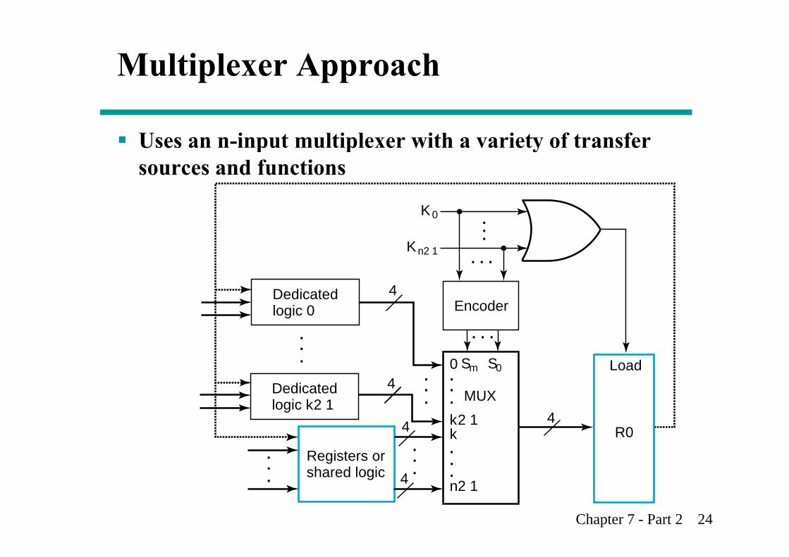
Multiplexer Approach
Uses an n-input multiplexer with a variety of transfer p p ysources and functions
K0 .... . .
0
Kn2 1
Dedicatedlogic 0 Encoder
. . . .
4
Dedicatedlogic k2 1
.
.
....
.
.
MUX
Sm S0 Load4
0
logic k2 1
.
...
.
.
k2 1k
Registers orh d l i
4 R04
Chapter 7 - Part 2 24
... .
n2 1shared logic 4

Multiplexer Approach
Load enable by OR of control signals K0, K1, … Kn-1f 00 0- assumes no load for 00…0
Use:E d M l i l ( h )• Encoder + Multiplexer (shown) or
• n x 2 AND-OR
to select sources and/or Kto select sources and/ortransfer functions
D di t d
.... . .
K0
Kn2 1
4Dedicatedlogic 0 Encoder
.
.
. Sm S0 Load
. . .
4
0
Dedicatedlogic k2 1
.
.
....
. .
MUXk2 1k
Registers or
4
4 R04
Chapter 7 - Part 2 25
.
....
.
.n2 1
Registers orshared logic 4
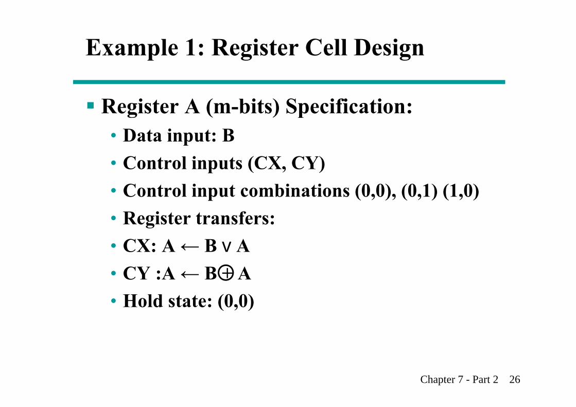
Example 1: Register Cell Design
Register A (m-bits) Specification:Register A (m bits) Specification:• Data input: B
C t l i t (CX CY)• Control inputs (CX, CY)• Control input combinations (0,0), (0,1) (1,0)• Register transfers:• CX: A ← B v ACX: A ← B v A• CY :A ← B + A
H ld t t (0 0)• Hold state: (0,0)
Chapter 7 - Part 2 26

Example 1: Register Cell Design (continued)
Load ControlLoad = CX + CY
Since all control combinations appear as if d d (0 0) (0 1) (1 0) l i lencoded (0,0), (0,1), (1,0) can use multiplexer
without encoder:S1 CXS1 = CXS0 = CYD0 = Ai Hold Ai D1 = Ai ← Bi + Ai CY = 1D2 = Ai ← Bi v Ai CX = 1
N t th t th d d t f th 3 i tNote that the decoder part of the 3-input multiplexer can be shared between bits if desired
Chapter 7 - Part 2 27
desired

Sequential Circuit Design Approach
Find a state diagram or state tableg• Note that there are only two states with the state
assignment equal to the register cell output valueassignment equal to the register cell output valueUse the design procedure in Chapter 6 to
l t th ll d icomplete the cell designFor optimization:p• Use K-maps for up to 4 to 6 variables• Otherwise use computer aided or manual• Otherwise, use computer-aided or manual
optimization
Chapter 7 - Part 2 28
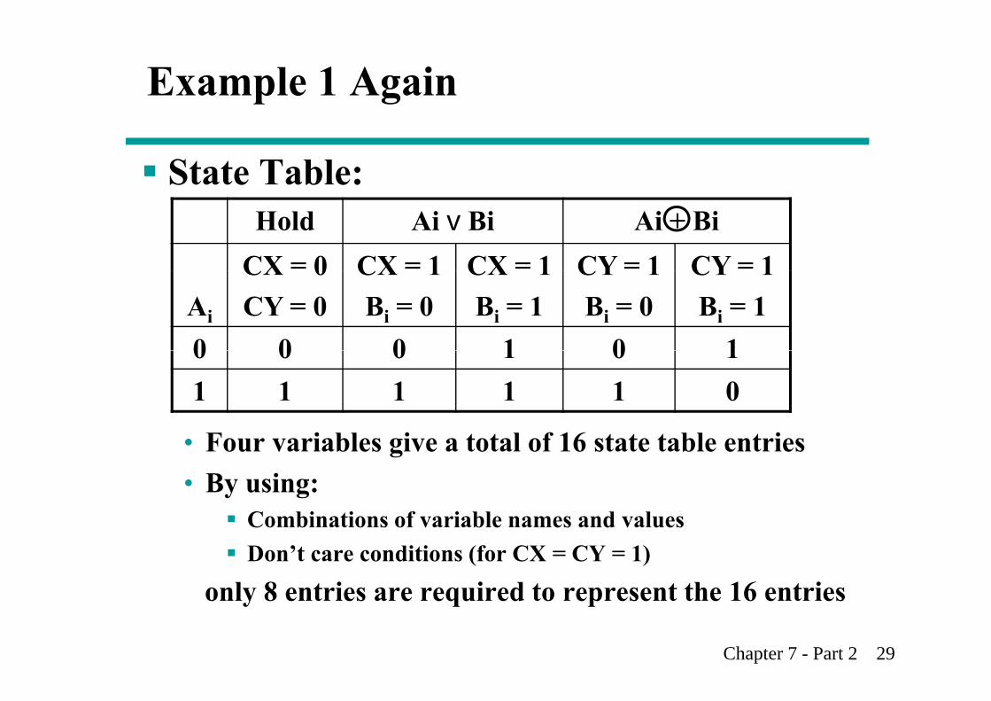
Example 1 Again
State Table:Hold Ai v Bi Ai + Bi
CX = 0 CX = 1 CX = 1 CY = 1 CY = 1Ai
CX 0CY = 0
CX 1Bi = 0
CX 1Bi = 1
CY 1Bi = 0
CY 1Bi = 1
0 0 0 1 0 10 0 0 1 0 11 1 1 1 1 0
• Four variables give a total of 16 state table entries• By using:
Combinations of variable names and valuesDon’t care conditions (for CX = CY = 1)
only 8 entries are required to represent the 16 entries
Chapter 7 - Part 2 29
only 8 entries are required to represent the 16 entries
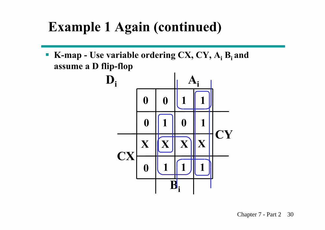
Example 1 Again (continued)
K-map - Use variable ordering CX, CY, Ai Bi and f i fassume a D flip-flop
AiDi
100 1
CYXX XX
0 11 0
CXX X XX
0 11 1
Bi
0 11 1
Chapter 7 - Part 2 30

Example 1 Again (continued)
The resulting SOP equation:D CX B CY A B A B CY ADi = CX Bi + CY Ai Bi + Ai Bi + CY Ai
Using factoring and DeMorgan’s law:D CX B A (CY B ) A (CY B )Di = CX Bi + Ai (CY Bi) + Ai(CY Bi )Di = CX Bi + Ai + (CY Bi)
The gate input cost per cell = 2 + 8 + 2 + 2 = 14The gate input cost per cell = 2 + 8 + 2 + 2 = 14The gate input cost per cell for the previous version is:version is:
Per cell: 19 Shared decoder logic: 8Shared decoder logic: 8
Cost gain by sequential design > 5 per cellAlso no Enable on the flip-flop makes it cost less
Chapter 7 - Part 2 31
Also, no Enable on the flip-flop makes it cost less
Multiplexer and Bus-Based Transfers for Multiple RegistersMultiple Registers
Multiplexer dedicated to each registerMultiplexer dedicated to each registerShared transfer paths for registers• A shared transfer object is a called a bus
(Plural: buses)Bus implementation using:• multiplexers• multiplexers • three-state nodes and drivers
In most cases, the number of bits is the length of the receiving register
Chapter 7 - Part 2 32
g g g

Dedicated MUX-Based Transfers
Multiplexer connected S0 L0
pto each register input produces a very
n
nMUXS0
1
n
R0
Load
p yflexible transfer structure => S1 L1
Characterize the simultaneous transfers
n
nMUXS0
1
n
R1
Load
simultaneous transfers possible with this structure S2 L2structure.
n
nMUXS0
1
n
R2
Load
Chapter 7 - Part 2 33
1 R2

Multiplexer Bus
A single bus driven byL0
A single bus driven by a multiplexer lowers cost, but limits the
nR0
Load
cost, but limits the available transfers =>Characterize the n S1 S0
0
S0S1L1
Characterize the simultaneous transfers possible with this
nMUX
01
n 2
nR1
Loadn
pstructure. Characterize the cost L2
savings compared to dedicated multiplexers
nR2
Load
Chapter 7 - Part 2 34

Three-State Bus
The 3-input MUX can be L0
replaced by a 3-state node (bus) and 3-state buffers.
n
R0
Load
nCost is further reduced, but transfers are limitedCh t i th
L1E0
Characterize the simultaneous transfers possible with this n
n
R1
Load
possible with this structure. Characterize the cost L2E1
savings and compareOther advantages?
n
R2
Load
n
Chapter 7 - Part 2 35E2
Serial Transfers and Microoperations
Serial Transfers• Used for “narrow” transfer paths• Example 1: Telephone or cable line
P ll l t S i l i tParallel-to-Serial conversion at sourceSerial-to-Parallel conversion at destination
• Example 2: Initialization and Capture of the contents ofExample 2: Initialization and Capture of the contents of many flip-flops for test purposes
Add shift function to all flip-flops and form large shift registerUse shifting for simultaneous Initialization and Capture operations
Serial microoperationsSerial microoperations• Example 1: Addition• Example 2: Error-Correction for CDs
Chapter 7 - Part 2 36
Example 2: Error Correction for CDs

Serial Microoperations
By using two shift registers for operands, a full adder, and a fli fl (f h ) dd b i llflip flop (for the carry), we can add two numbers serially, starting at the least significant bit.Serial addition is a low cost way to add large numbers ofSerial addition is a low cost way to add large numbers of operands, since a “tree” of full adder cells can be made to any depth, and each new level doubles the number ofany depth, and each new level doubles the number of operands.Other operations can be performed serially as well, such as p p y ,parity generation/checking or more complex error-check codes.Shifting a binary number left is equivalent to multiplying by 2.
Chapter 7 - Part 2 37
Shifting a binary number right is equivalent to dividing by 2.
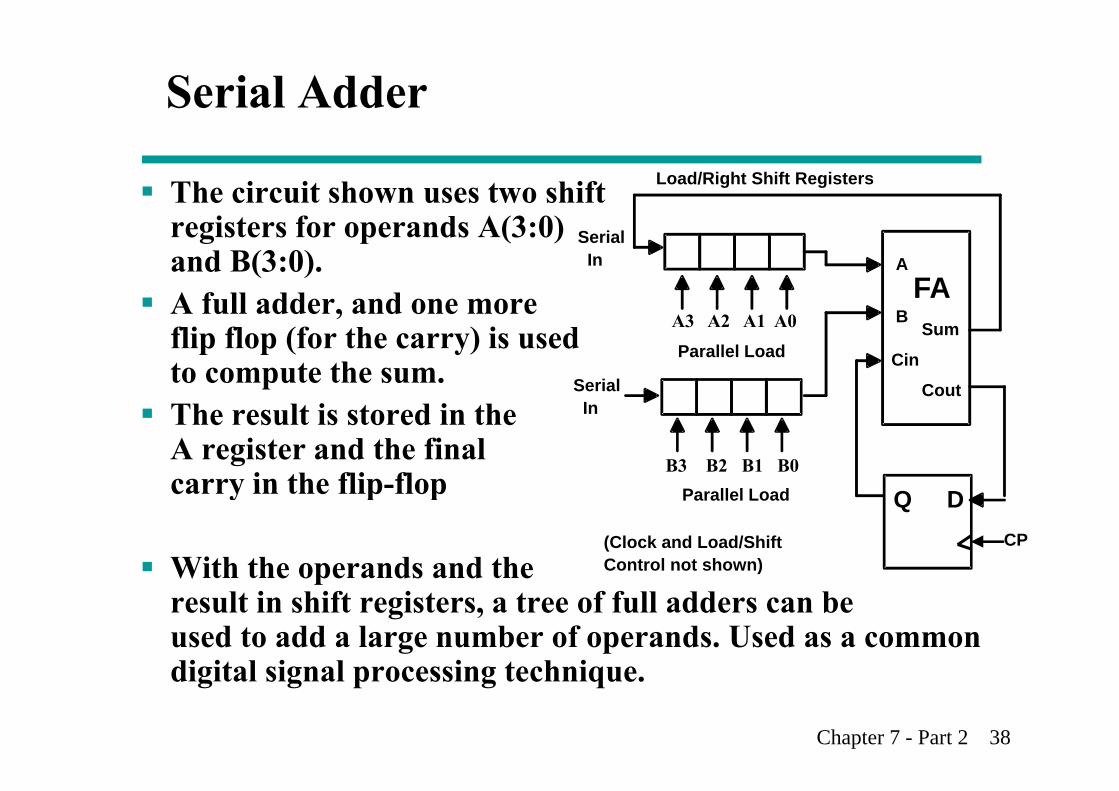
Serial Adder
The circuit shown uses two shifti f d A(3 0)
Load/Right Shift Registers
registers for operands A(3:0)and B(3:0).A full adder and one more
AFA
SerialIn
A full adder, and one moreflip flop (for the carry) is usedto compute the sum.
A3 A2 A1 A0 B
Cin
Sum
CoutSerial
Parallel Load
The result is stored in theA register and the finalcarry in the flip-flop
B3 B2 B1 B0
CoutIn
carry in the flip-flop
With the operands and the
DQCP
Parallel Load
(Clock and Load/ShiftControl not shown)With the operands and the
result in shift registers, a tree of full adders can beused to add a large number of operands. Used as a common di it l i l i t h i
Chapter 7 - Part 2 38
digital signal processing technique.

Terms of Use
© 2004 by Pearson Education,Inc. All rights reserved.The following terms of use apply in addition to the standard Pearson Education Legal Notice.Permission is given to incorporate these materials into classroomPermission is given to incorporate these materials into classroom presentations and handouts only to instructors adopting Logic and Computer Design Fundamentals as the course text. Permission is granted to the instructors adopting the book to post these materials on a protected website or protected ftp site in original or modified form. All other website or ftp postings, including those offering the materials for a fee, are prohibited. You may not remove or in any way alter this Terms of Use notice or any trademark copyright or other proprietary notice including theany trademark, copyright, or other proprietary notice, including the copyright watermark on each slide. Return to Title Page
Chapter 7 - Part 2 39
Related Documents