Chapter 4 Bipolar junction transistor 1

Welcome message from author
This document is posted to help you gain knowledge. Please leave a comment to let me know what you think about it! Share it to your friends and learn new things together.
Transcript

Chapter 4
Bipolar junction transistor
1

Objectives
• Describe the basic structure of the bipolar junction
transistor (BJT)
• Explain and analyze basic transistor bias and
operationoperation
• Discuss the parameters and characteristics of a
transistor and how they apply to transistor circuits
2

�What is transistor?� three-terminal device whose output current, voltage and/or
power are controlled by its input.
� 2 basic transistor types: BJT and FET
Transistor
3

Transistor Construction
There are two types of transistors:• pnp
• npn
The terminals are labeled:
• E – Emitter
• B - Base
• C - Collector
pnp
• C - Collector
npn
4

Transistor Operation
Biasing:
• two pn junction must be correctly biased with external dc voltages to operate the
transistor properly.
• The figure shown the proper bias arrangement for both npn and pnp transistor for
active operation as an amplifier.
5

Transistor Operation
Transistor Voltages:
• VCC – collector supply voltage. This is a power supply voltage applied directly to
collector of transistor.
• VBB – base supply voltage. this is dc voltage used to bias base of transistor.
• VEE – emitter supply voltage. dc biasing voltage and in many cases, VEE is simply a
ground connection.
6

Transistor Operation
Transistor Voltages:
• VC – dc voltage measured from collector terminal of component to ground
• VB – dc voltage measured from base terminal to ground.
• VE – dc voltage measured from emitter terminal to ground.
7

Transistor Operation
Transistor Voltages:
• VCE – dc voltage measured from collector to emitter terminal of transistor.
• VBE – dc voltage measured from base to emitter terminal of transistor.
• VCB – dc voltage measured from collector to base terminal of transistor.
8

Currents in a Transistor
Emitter current is the sum of the collector and base currents:
Current gain (β) � factor by which current increases from base of transistor to its
collector.
CBE III +=
II β=
9
BDCC II β=

Operating Regions
• Active – Operating range of the amplifier.
• Cutoff – The amplifier is basically off. There is voltage, but little current.
• Saturation – The amplifier is full on. There is current, but little voltage.
10

Operating Regions
Cutoff region
• Both transistor junctions are
reverse biased.
• With large depletion region
between C-B and E-B, reverse
current, I passes from emittercurrent, ICEO passes from emitter
to collector and can be neglected.
• So, VCE = VCC
11

Operating Regions
Saturation region
• Both transistor junctions are
forward-biased.
• IC reaches its maximum value as
determined by VCC and total
resistance in C-E circuit.resistance in C-E circuit.
• IC is independently from
relationship of β and IB.
• VBE is approximately 0.7V and
VCE < VBE.
EC
CC
CRR
VI
+=
12

Operating Regions
Active region
• BE junction is forward biased
and the BC junction is reverse
biased.
• All terminal currents have some
measurable value.measurable value.
• The magnitude of IC depends on
the values of β and IB.
• VCE is approximately near to 0.7V
and VCE falls in ranges
VBE<VCE<VCC.
13

Operating Regions
Transistor Operating Regions:
1.Cutoff region:
� Both transistor junctions are reverse biased
� All terminal current are approximately equal
to zero. Since ICEO neglected, VCE = VCC
2.Active region:
� The BE junction is forward biased and the BC junction is reverse biased� The BE junction is forward biased and the BC junction is reverse biased
� All terminal currents have some measurable value
� The magnitude of IC depends on the values of and IB
� VCE is approximately near to 0.7V and VCE falls in ranges VBE<VCE<VCC
3.Saturation:
� Both transistor junctions are forward biased
� IC reaches its maximum values- determine by
the component in the CE circuit, and independent
of the values of and IB
� VBE is approximately 0.7V and VCE < VBEβ
β
14

Approximations
Emitter and collector currents:
I ≅ I C E
Base-emitter voltage:
VBE = 0.7 V (for Silicon)
15

Alpha (αααα)
Alpha (α) is the ratio of IC to IE :
IE
α
I
= Cdc
Ideally: α = 1Ideally: α = 1
In reality: α is between 0.9 and 0.998
16

Beta (ββββ)
In DC mode:
β represents the amplification factor of a transistor. (β is sometimes referred
to as hfe, a term used in transistor modeling calculations)
β =IC
IB
dc
Relationship between amplification factors β and α
17
β
β + 1α =
α
α − 1β =
Relationship Between Currents
IC = βIB IE = (β + 1)IB

Current and Voltage Analysis:
� When the BE junction is forward-biased, like a forward biased
diode and the voltage drop is
� Since the emitter is at ground (0V), by Kirchhoff’s voltage law, the
voltage across is: …….(1)
VVBE 7.0≅
BR BEBBR VVVB
−=
BJT CHARACTERISTICS & PARAMETERS
voltage across is: …….(1)
� Also, by Ohm’s law: ……..(2)
� From (1) ->(2) :
� Therefore, the dc base current is:
BR BEBBR VVVB
−=
BBR RIVB
=
BBBEBB RIVV =−
B
BEBBB
R
VVI
−=
18

Current and Voltage Analysis:
• The voltage at the collector with respect to the grounded emitter is:
• Since the drop across is:
CRCCCE VVV −=
R CCRC RIV =
BJT CHARACTERISTICS & PARAMETERS
• Since the drop across is:
• The dc voltage at the collector with respect to the emitter is:
• where
• The dc voltage at the collector with respect to the base is:
CCCCCE RIVV −=
BECECB VVV −=
CR CCRC RIV =
BDCC II β=
19
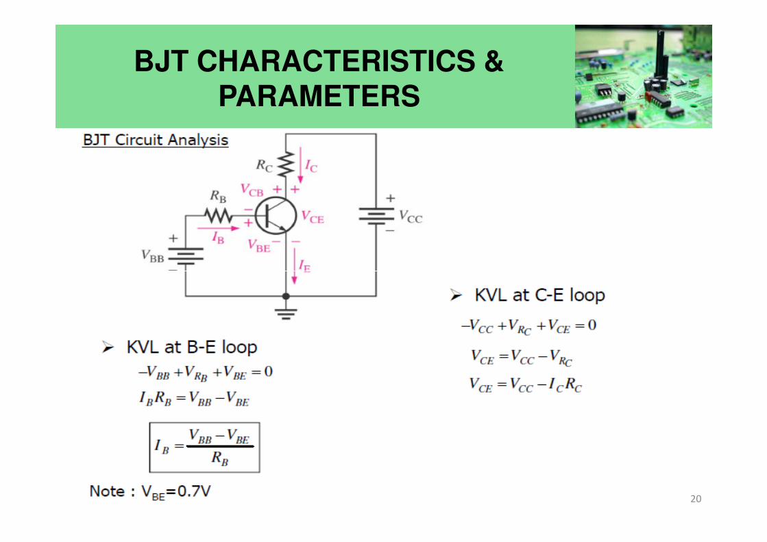
BJT CHARACTERISTICS & PARAMETERS
20

DC Load Line:
� Cutoff and saturation can be illustrated in relation to the collector characteristiccurves by the use of a load line.
� DC load line drawn on the connecting cutoff and saturation point.
� The bottom of load line is ideal cutoff where IC=0 & VCE=VCC.
� The top of load line is saturation
BJT CHARACTERISTICS & PARAMETERS
� The top of load line is saturation
where IC=IC(sat) & VCE =VCE(sat)
� In between cutoff and saturation
is the active region of transistor’s
operation.
21

BJT CHARACTERISTICS & PARAMETERS
Collector Characteristic Curve:
22

A transistor when used as a switch is simply being biased so that it is in:
1. cutoff (switched off)
2. saturation (switched on)
BJT AS A SWITCH
23

Conditions in Cutoff
CCcutoffCE VV =)(
Neglect leakage current and all currents
are zero. BE junction is reverse biased.
BJT AS A SWITCH
C
satCECCsatC
R
VVI
)()(
−=
DC
satCB
II
β
)((min) =
Conditions in Saturation
Since VCE(sat) is very small compared to
VCC, it can be neglected.
24
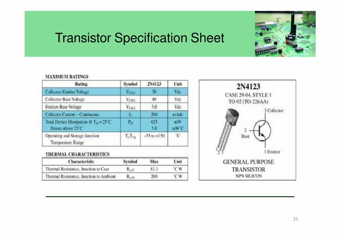
Transistor Specification Sheet
25

Transistor Specification Sheet
26

Transistor Testing
• Curve Tracer
Provides a graph of the characteristic
curves.
• DMM
Some DMMs measure βDC or hFE.
• Ohmmeter
27

Transistor Terminal Identification
28
Related Documents

![UNIVERSITI MALAYSIA PERLISportal.unimap.edu.my/portal/page/portal30/STD_ACA_BULL...Teori Litar Elektrik [Electric Circuit Theory] 9.00 pagi (am) 3 jam (hours) DKD 4 EKT112 Prinsip-prinsip](https://static.cupdf.com/doc/110x72/60d5df26c10ff54a770fff61/universiti-malaysia-teori-litar-elektrik-electric-circuit-theory-900-pagi.jpg)


![UNIVERSITI MALAYSIA PERLISportal.unimap.edu.my/portal/page/portal30/STD_ACA... · Prinsip -prinsip Pengurusan [Principles Of Management] 9.00 pagi (am) 3 jam (hours) DSKG DKG 3 DKG](https://static.cupdf.com/doc/110x72/5e48859838368360262be250/universiti-malaysia-prinsip-prinsip-pengurusan-principles-of-management-900.jpg)