CHAPTER 4 PWM SCHEMES IN THREE PHASE VOLTAGE SOURCE INVERTERS APPLIED TO CURRENT SOURCE INVERTERS 4.1 Introduction Due to the inability of VSI to regenerate the incoming AC supply in absence of complex rectifying converter, there are large d v /d t transitions on the phase leg output voltages. This results in conspicuous problems as increased motor losses, acoustic noise in load, insulation degradation due to voltage surges and electromagnetic interference effects (EMI). Three-phase Current Source Inverter as in figure 4.1 (CSI) has distinct advantage over Voltage Source Inverter (VSI) drives primarily due to following reasons: 1. The drive is current sensitive. Torque is directly related to stator current and rather nonlinearly with stator voltage. c S ap S an S bp S bn S cn Lf Co Vo[abc] Idc Cop[abc] Io[abc] Il[abc] PWM CSI Output Filter Load Induction Motor S cp Vdc b a Figure 4.1 Topology of a current source inverter in motor drive application

Welcome message from author
This document is posted to help you gain knowledge. Please leave a comment to let me know what you think about it! Share it to your friends and learn new things together.
Transcript

CHAPTER 4
PWM SCHEMES IN THREE PHASE VOLTAGE SOURCE INVERTERS
APPLIED TO CURRENT SOURCE INVERTERS
4.1 Introduction
Due to the inability of VSI to regenerate the incoming AC supply in absence of complex
rectifying converter, there are large dv/dt transitions on the phase leg output voltages. This
results in conspicuous problems as increased motor losses, acoustic noise in load,
insulation degradation due to voltage surges and electromagnetic interference effects
(EMI).
Three-phase Current Source Inverter as in figure 4.1 (CSI) has distinct advantage over
Voltage Source Inverter (VSI) drives primarily due to following reasons:
1. The drive is current sensitive. Torque is directly related to stator current and
rather nonlinearly with stator voltage.
c
Sap
San
Sbp
Sbn Scn
Lf
Co
Vo[abc]
Idc
Cop[abc]
Io[abc] Il[abc]
PWM CSI
OutputFilter
Load Induction Motor
Scp
Vdc
ba
Figure 4.1 Topology of a current source inverter in motor drive application

80
2. The drive is regenerative. Hence the control of current ensures the direct and
precise control of the electromagnetic torque. Pulse width modulation (PWM)
current source inverter (CSI) fed ac motor drives are often used in high power
(1,000–10 000 hp) applications. The CSI drive has the features of simple
structure:
1. Reliable short circuit protection
2. Four quadrant operation capability and nearly sinusoidal outputs.
3. Low output dv/dt resulting from filtering effect of output capacitors.
4. In addition, the switching device [symmetrical GTO or gate commutated thyristor
(GCT)] used in the CSI can be easily connected in series, which makes the CSI
drive particularly suitable for implementation at medium voltage (2300 V–7200
V) levels.
These advantages outweigh the other disadvantages of the CSI topology.
The Current Source PWM Rectifier can be used as the front end as a DC link source. The
rectifier can be operated at unity power factor. Figure 4.2 shows the schematic diagram of
a PWM CSR and CSI fed induction motor drive.
As compared with VSI there is intense need for developing modulation and control
strategies for CSI. The performance of CSI in very high power applications still holds
good essentially due to the ruggedness and ability to meet load demands easily.
The six-step or square wave inverters switching leads to large amount of harmonics in
load voltage and current, the widespread application of this inverter has been curbed [1].

81
The PWM CSI are feasible with the advent of GTO’s, but due to the restriction on
switching speed, this approach has limited application. Hence the PWM CSI are less
common in practice than VSI PWM inverters, in comparison with a square wave inverter.
PWM CSI topology has the output filter capacitors to remove the harmonics due to the
switching currents [4.1]. Topologies as shown in Figure 4.1 wherein the IGBT is in series
with the diode has distinct disadvantage of low efficiency because in every period of
conduction, the total loss is loss in series diode and IGBT which is twice much higher
than that in VSI counterpart in very high power applications.
In spite of these drawbacks, the performance of CSI with IGBT in series with diode is
being explored with high performance adaptive PWM algorithms. It should be possible to
stretch the performance of these topologies to obtain high quality AC waveforms along
with higher output power by utilizing various or adaptive PWM algorithms.
The following section will explore the utilization of the discontinuous PWM schemes as
applied in VSI into a CSI. This will also cover the gating requirements to avoid shorting
of adjacent legs, and the logic circuit development. The operation is studied with a
current source inverter with R-L load. The performance is examined through both
simulation and experimental results.

82
Lf
Idc
Load Induction Motor
Vr Vdc
PWM CSIPWM CSR
CoCi
3 Phase Supply
Controller3 Phase VSC to CSC mapping logic
Ia Ib Ic
Ia_refIb_refIc_ref
Controllersignals
Gatingpattern for
CSI
Gatingpattern for
CSR
Figure 4.2: Schematic of PWM CSR-CSI drive for induction machine
4.2 Previous PWM Schemes in three phase CSI
In VSI PWM schemes where in by adding zero sequence voltages to the existing
modulating signals in high modulation region, the switching loss, voltage linearity, and
over modulation performance of the inverter is optimized [4.16]. In a similar way if we
can adapt these modulation strategies into a CSI then the advantages of the modulation
schemes in VSI can be extended to a CSI.
The online carrier based PWM scheme [4.11-4.13] is the easiest to be
implemented. Using the state concepts developed for CSI and VSI it is clear that by any
CSI can be controlled by any VSI modulation strategy if the active states created by the
modulator are mapped to the stationary vectors and to the switching combinations

83
associated with these vectors. In developing this scheme, it is necessary to determine
how the CSI null state should be related to the modulator state outputs.
In case of VSI with every sine triangle comparison there is implicit transition
through the null states and thus is not a separate part of the modulation process. Whereas
in case of CSI there is no direct mapping of the sine triangle output for the corresponding
null states of a CSI. Hence the null states have to be defined explicitly. This chapter has
detailed explanation of this mapping scheme. The various issues confronted and its
solutions will be explicated.
As compared with VSI there is intense need for developing modulation and
control strategies for CSI. Previous work [4.1-4.4] shows that the CSI gating
requirements are more complex than those of the VSI. Most of the modulation schemes
are developed as dedicated schemes or offline programmed patterns to optimize
switching in contrast to mapping the required states from the VSI modulating schemes.
From the space vector perspective though the CSI and VSI are not exactly dual of each
other, one can actually map the VSI schemes in to CSI.
4.3 Development of the gating schemes for CSI.
In complying with Kirchoff’s voltage (KVL) and current (KCL) law, the VSI is
restricted in the sense that both the devices in a leg cannot be on at the same, else it
would result in shorting of the DC link capacitor. But it does allow the shorting of the
adjacent legs. Similarly for CSI it is mandatory that only one device in the top and only
one in the bottom is on at a time, else the output capacitors will be shorted but it does

84
allow the shorting of the same leg. Table 4.1 gives the switching states available in a
voltage source converter while Table 4.2 gives the switching states available in a current
source converter.
Table 4.1 : Switching States in a 3 phase VSI
State Sap Sbp Scp San Sbn Scn
Null, S0 0 0 0 1 1 1 San Sbn Scn
S1 0 0 1 1 1 0 Scp San Sbn
S2 0 1 0 1 0 1 Sbp San Scn
S3 0 1 1 1 0 0 Sbp Scp San
S4 1 0 0 0 1 1 Sap Sbn Scn
S5 1 0 1 0 1 0 Sap Scp Sbn
S6 1 1 0 0 0 1 Sap Sbp Scn
Null, S7 1 1 1 0 0 0 Sap Sbp Scp

85
Table 4.2 : Switching States in a 3 phase CSI
State h1 h2 h3 h4 h5 h6
h1h2 1 1 0 0 0 0
h2h3 0 1 1 0 0 0
h3h4 0 0 1 1 0 0
h4h5 0 0 0 1 1 0
h5h6 0 0 0 0 1 1
A
C
T
I
V
E
h6h1 1 0 0 0 0 1
h1h4 1 0 0 1 0 0
h2h5 0 1 0 0 1 0
N
U
L
L h3h6 0 0 1 0 0 1
The active states are used to produce the required output voltages while the null states are
used to remove the energy stored in the input inductor.
The objective here is to obtain Tables 4.2 and 4.1 subject to the following
conditions of KVL and KCL these can be laid out as:
1=++ cpbpap SSS ,
1=++ cnbnan SSS (4.1)
another necessary condition is that the product of any of the top 2 devices at any given
time should always be zero.
0. =bpap SS , , 0. =cpbp SS 0. =cpap SS (4.2)
0. =bnan SS , , 0. =cnbn SS 0. =cnan SS (4.3)

86
The KVL and KCL conditions pre-applied to voltage source inverter are:
, , 1=+ anap SS 1=+ bnbp SS 1=+ cncp SS (4.4)
and
0. =anap SS
0. =bnbp SS
0. =cncp SS (4.5) The 8 feasible switching modes of the three phase VSI are given in Table 4.1 . The
stationary reference frame qdo voltages of the switching modes are expressed in the
complex variable form as ( a = ejβ, β = 120°) :
Vqds =2/3(Van +aVbn+a2Vcn) , Vo = 1/3(Van +Vbn + Vcn). (4.6)
Using the phase to reference voltages Vao, Vbo, and Vco for each switching mode, the
components of the stationary reference frame Vqdos expressed in terms of the switching
functions are given as :
Vqs =1/6( 2Sap– Sbp – Scp - 2San + Sbn+ Scn)Vd ,
Vds = 1/2√3(Scp–Sbp – Scn + Sbn)Vd , (4.7)
Vo =1/6(Sap+ Sbp+ Scp - San - Sbn - Scn )Vd
Sip and Sin for i =a,b,c are the switching functions of top (p) and bottom (n) for the
phases. Based on the stationary reference frame q-d-o voltages and currents space vector
diagrams, one can observe the relevance between the VSI and CSI. It is notable that there
is one to one correspondence between the active states of VSI and CSI.

87
12
3
4 5
6
]3
[ ,d
dII
]3
2,0[ dI
]3
[ ,d
dI
I−
]3
[ ,d
dI
I −−
]3
2,0[ dI−
]3
[ ,d
dII −
][ , b na p SS
][ , b nc p SS
][ , a nc p SS
][ , a nb p SS
][ , c nb p SS
][ , c na p SS
q dI
(a)
*qdv
6V,
3V,
3V ddd
−
6V,0,
3V2 dd
U2 (++-)(-+-)U3
U4
(-++)
(--+)(+-+)
(+--)
U1
U5U6
jIm
I
II
III
IV
V
VI
−−
6V,
3V,
3V ddd
−
6V,0,
3V2 dd
−−
6V,
3V,V ddd
3−
−6V,
3V,
3V ddd
cnbnap SSS.
cnbpap SSS.cpbnan SSS.
cpbpan SSS.
cnbpan SSS.cpbnap SSS.
(b)
Figure 4.3 3-D Plot of Stationary qdo voltages and currents for the given states of
(a) CSI (b) VSI
88
Figure 4.3 (b) shows eight possible space vectors for VSI of which 6 are active
states and two are null states. As shown in Figure 4.3(a) CSI have nine possible space
vectors of which six are active and three are null vectors. It is conspicuous that the angles
between active space vectors are 60° for VSI and CSI and the CSI space vector lead the
VSI space vector by 30 in an absolute sense [13]. From [9], there is one to one
correspondence between the active states of VSI and CSI, hence the mapping is simple.
Table 4.3: Switching modes of the three-phase voltage source inverter and
corresponding stationary reference frame qdo voltages.
Mode Sap Sbp Scp Vqs Vds Vos 1 0 0 0 0 0 -Vd/2 2 0 0 1 -Vd/√3 Vd/√3 -Vd/6 3 0 1 0 -Vd/3 -Vd/√3 -Vd/6 4 0 1 1 -2Vd/3 0 Vd/6 5 1 0 0 2Vd/3 0 -Vd/6 6 1 0 1 Vd/3 -Vd/√3 Vd/6 7 1 1 0 Vd/3 Vd/√3 Vd/6 8 1 1 1 0 0 Vd/2

89
Table 4.4: Switching modes of the three-phase current source inverter and
corresponding stationary reference frame qdo currents.
ON Device
ON Device Ias Ibs Ics Iqq √3 Idd
bnS Id - Id 0 Id Id
apS cnS. Id 0 - Id Id - Id
bpS anS - Id Id 0 - Id - Id
bpS cnS 0 Id - Id 0 - 2Id
cpS anS - Id 0 Id - Id Id
cpS bnS 0 - Id Id 0 2Id
apS anS 0 0 0 0 0
bpS bnS 0 0 0 0 0
cpS cnS. 0 0 0 0 0
apS
4.4 Mapping technique
From Table 4.1 and 4.2 the mapping procedure is done as follows:
Consider the output state we desire from the available input states. If we combine the VSI
states in a particular way we can obtain the desired output states, thus:
311 SSh += (4.8)
taking the complement of both sides we have
311 SSh +=
ancpbpbnancp SSSSSSh +=1

90
)(1 bpbnancp SSSSh += (4.9)
now using the property of
BABA +=. and BABA .=+ we have,
bpbnapcnbpbnancpbpbnancp SSSSSSSSSSSSh +=+=++= .)(1
using the property BABA ... = we have
bpbnapcn SSSSh +=1 . (4.10)
Here the first term corresponds to the active state while the second term corresponds to a
null state in CSI. The remaining CSI states are listed as:
apanbpcn SSSSh +=2 (4.11)
cpcnanbp SSSSh +=3 (4.12)
bpbnancp SSSSh +=4 (4.13)
apanbncp SSSSh +=5 (4.14)
cpcnapbn SSSSh +=6 (4.15)
It is evident from these expressions that any VSI state combination results in a
combination of a CSI active state and a null state. The truth tables for the expressions are
summarized in Table 4.5.

91
Table 4.5 Derivation of the desired states from the available states
h1 h2 h3 h4 h5 h6 Sap Sbp Scp San Sbn Scn SapScn+
SbpSbn
SbpScn+
SapSan
SbpSan+
ScpScn
ScpSan+
SbpSbn
ScpSbn+
SapSan
SapSbn+
ScpScn
0 0 0 1 1 1 0 0 0 0 0 0
0 0 1 1 1 0 0 0 0 1 1 0
0 1 0 1 0 1 0 1 1 0 0 0
0 1 1 1 0 0 0 0 1 1 0 0
1 0 0 0 1 1 1 0 0 0 0 1
1 0 1 0 1 0 0 0 0 0 1 1
1 1 0 0 0 1 1 1 0 0 0 0
1 1 1 0 0 0 0 0 0 0 0 0
From the Table 4.5 it can be noted that only one device in the top and bottom is
ON at any given time. However according to condition given by Equation 4.4 it is
evident that this null state can never be mapped in CSI because the output of this product
term will always be zero. This scheme as on its own can be used for generating the gating
signals for a CSI but it won’t allow the utilization of the available three null states SapSan,
SbpSbn, and ScpScn of the CSI.
4.6 Shorting Pulses and its Distribution
There is a necessity to introduce the null states in conjunction with the active
states. Thus an additional condition for minimization of the number of switch transitions,
,maintain balanced switch utilization and reduction of losses can be imposed

92
[4.11],[4.12]. This should also ensure the symmetry in the output switched currents in
order to have minimum harmonic distortion. To satisfy the above requirement a logic
circuit is developed to detect the condition when the null state has to be applied. This
logic circuit detects a NULL state whenever all the devices in the top and/or bottom are
found to be zero. This condition corresponds to the highlighted section in Table 4.5. Once
the condition for null state is detected one of the three legs of the CSI has to be shorted.
This is done by gating the devices in the same leg by a common signal, which will be
termed as a shorting pulse.
From the VSI states the occurrence of the null states causes a train of shorting
pulses hence the main issue arising here is the distribution of these shorting pulses in the
given cycle. In order to have minimum harmonics on the output waveform, the
distribution has to be symmetric. Hence we refer back to Table 4.6 and Figure 4.5 to
study this aspect. It is known that in a three- phase system each phase voltage is
maximum/minimum for 120° in every cycle. If the line-line voltages are considered, then
the maximum/minimum is 120° but distributed 60° in a cycle. This 60° distribution is
essential for generation of symmetric output current waveforms. For example, Vap has its
maximum occurring in sector I for 60° and VI for 60°, thus the effective period for which
the amplitude of Vap is maximum is 120° but it is distributed by 60° in a cycle. It is also
known that this sequence can be achieved using the absolute maximum of the line-line
voltages of the reference signals.

93
S p a
S p b
S p c
V a b V b c V c a V a b V b c V c a
S h o r t -L e g A
S h o r t -L e g B
S h o r t -L e g C
S h o r t -L e g A
S h o r t -L e g B
S h o r t -L e g C
A b s o l u t e M a x i m u m o f l i n e - l i n e v o l t a g e s
Figure 4.4 Generation of the Distribution pulses for shorting a leg in CSI Table 4.6: Device Switching times expressed in terms of reference line-line voltages
Sector I II III IV V VI
Max Volt Vap Vbp Vbp Vcp Vcp Vap
Min Volt Vcp Vcp Vap Vap Vbp Vbp
Abs max (Vab, Vbc, Vca)
Vab, Vbc, Vca
Van, Vbn, and Vcn
Figure 4.5 Generation of distribution logic for the NULL states
94
One can get the same result as explained above by the use of absolute maximum
of line-line voltages. Using maximum of phase voltages Van, Vbn, and Vcn will give a
distribution of 120° in a cycle, but this results in asymmetric output currents. It will result
in half wave symmetry and eventually more harmonics on the output currents. Thus the
using absolute maximum of line-line voltages is a better option so that when line-line
voltage Vab is maximum we short leg ‘A’, Vbc is maximum we short leg B, Vca is
maximum we short leg C.
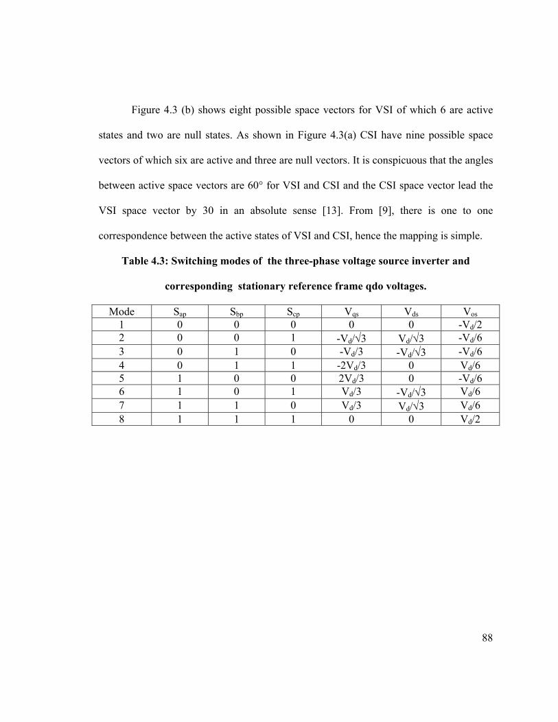
4.7 Practical scheme layout and gating pattern signals
Figure 4.6 shows the practical scheme for implementing the VSI to CSI mapping.
The PWM switching signals obtained from the output of the DSP are recombined to
generate Table 4.1. Thus S1 through S7 are the outputs of the logic gates corresponding to
the VSI states. These states are recombined using equations 4.8 through 4.13 to obtain the
states listed in Table 4.2.
The third condition is for the detection of null states and their distribution logic. The null
state logic detector activates Sd = 1 whenever sum of all the devices in the top and bottom
are found to be zero. This Sd in combination with the distribution logic generates shorting
pulses of the corresponding leg. The calculation of the absolute maximum of the
reference signals is done internally in the DSP to generate the distribution signals SpA,
SpB, and SpC.

95
S a p S b p S c p S a n S b n
S 1
3 P h a s e V S I S w itc h in gS ta te s fro m D S P +
S h o rtin g P u ls e W in d o wg e n e ra to r
S 2
S 3
S 4
S 5
S 6
h 2
h 3
h 4
h 5
h 6
h 1
S c 2
S c 3
S c 4
S c 5
S c 6
S c 1
S p AS p BS p C
S c n
S d
Figure 4.6 Implementation of the scheme as listed in Table 4.4

4.7.1 Gating pattern signals for developed scheme:
(a)
(b) (c )
Figure 4.7 Experimental results generation of gating signals
Figure 4.7 (a) and similarly Scope 3 shows the generation of VSI switching states for Sap.
Scope 1 is the distribution logic pulse SpA, which corresponds to maximum is AB
amongst Absolute max (Vab, Vbc, Vca). Scope 4 is the occurrence of the null states during
the VSI operation. These shorting pulses are supposed to be distributed through
distribution pulses. Scope 2 is the final gating signal generated for the top device in
phase‘a’ of the CSI. Figure (c) shows the gating pulse for the top and bottom device,
and the generated current waveform. I = Id( - ) 1csiS 4csiS
97

98
4.8 Modeling of CSI in a-b-c reference frame
c
Sa p
S a n
Sb p
S b n Sc n
L
V a n
Id c
IaIa b c L
P W M C S I
O u tp u tF ilte r
S c p
V d c
b
aV r
Ib
Ic
V b n
V c nn
rL L l
C o
Figure 4.8 Modeling structure of a CSI
Table 4.7: Terminology used in modeling of CSI
Parameters Description
Vabcn Output phase voltages
Iabcn Output line currents
Iabcl Output load currents
Idc Input DC link current
Vdc Input source voltage
Vr Voltage at the output of the input inductor
Sabcp , Sabcn Top and bottom switching devices
rl , Ll Output load resistance and inductance
Co Output Filter capacitor

99
From Figure 4.7 the input DC voltage to the CSI is given as:
)()( cncnbnbnanancncpbnbpanapr VSVSVSVSVSVSV ++−++=
hence,
cncncpbnbnbpananapr VSSVSSVSSV )()()( −+−+−= (4.16)
Thus the drop across the DC link inductor is given as:
rdcdc VVLpI −= or
cncncpbnbnbpananapdcdc VSSVSSVSSVLpI )()()( −+−+−−= (4.17)
Now the unfiltered currents are given by
dcanapa ISSI )( −=
(4.18) dccncpc ISSI )( −=
dcbnbpb ISSI )( −=
The currents flowing through the output filter capacitor are given by
alaano IIpVC −=
blbbno IIpVC −=
clccno IIpVC −= (4.19)
and the load can be expressed as:
alLalLan pILIrV +=
blLblLbn pILIrV +=
clLclLcn pILIrV += (4.20)
Thus equations 4.16 through 4.20 can be used for simulating the CSI.

100
4.9 Simulation and Experimental Results
The simulation and experimental results were performed on a current source
inverter with an R-L load of 30 ohm and 4mH respectively at modulation index m = 0.96
and m = 1.5 (Over modulation). It can be seen that the experimental and simulation
results have a very close correspondence. The difference is be due to the inconsideration
of nonlinearties in the switching devices.
The objective was to observe the performance of various modulating schemes on
the inverter output voltages and currents. Hence the FFT of the filtered output voltage
and current was done to see the difference in the various PWM schemes.
It is observed that for a given ‘m’ all these schemes give the same fundamental output
voltages irrespective of the modulating schemes. Thus the only difference would lie in
the amount of device switching and the output waveform quality.
By studying the amount of actual switching performed in a cycle in each
modulation shows that space vector PWM with β = 0.5 has more switching than its
discontinuous counterparts to generate the same output voltages.
Following charts Figure 4.8 through 4.11 shows the plot of 3rd and 5th harmonics for each
voltage and currents for all the modulating schemes at m= 0.96 and over modulation.
The percent distortion depends on the load power factor. In this particular case the α = 0
has least harmonics in both the cases.
101
(a)
(b)
(c)
(d)
I Simulation II. Experiment
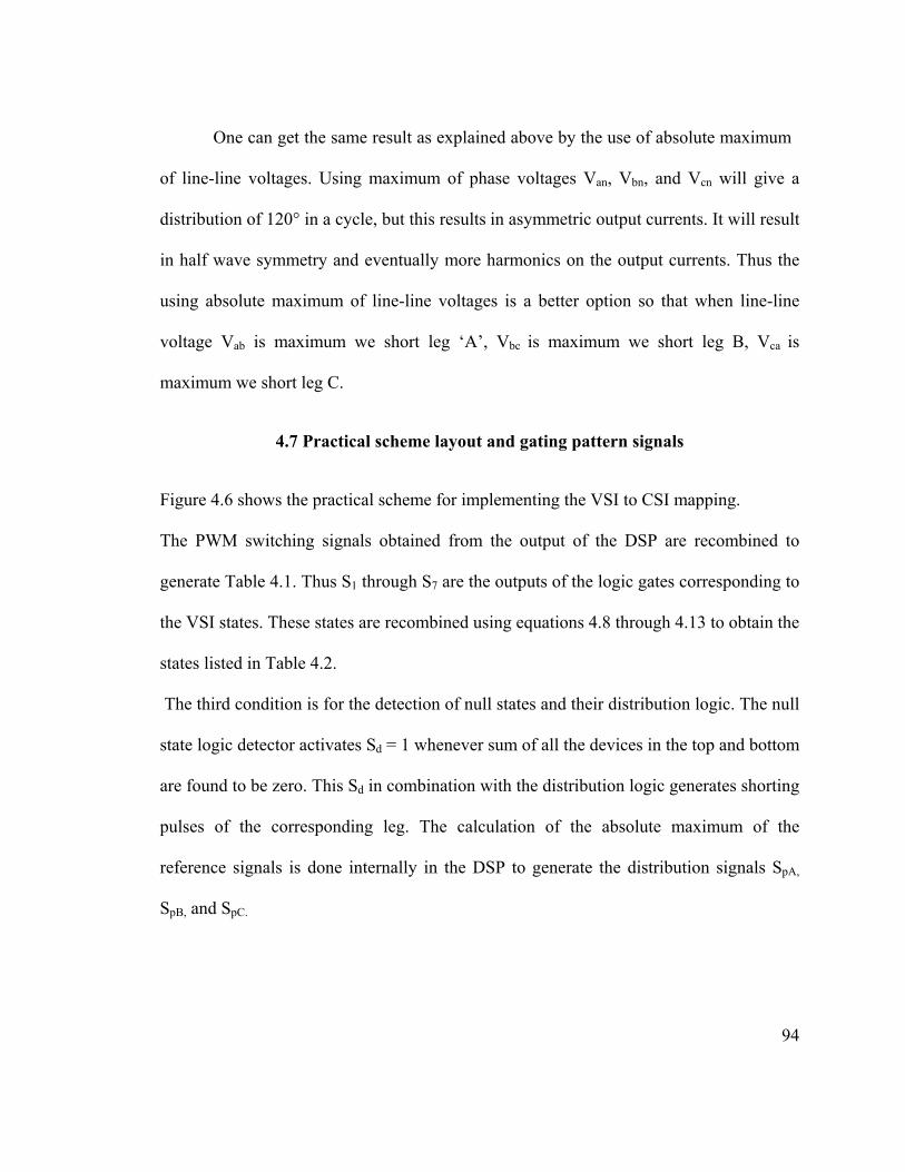
Figure 4.9 I & II Simulation and Experimental results respectively for three phase
CSI under GDPWM β = 0 modulation feeding an R-L load of ,RL = 30Ω,L = 4mH
at M = 0.96,Vdc = 40V, Idc = 1.8A (a)GDPWM modulating signal and corresponding
VSI switching (b)Unfiltered Phase ‘a’ Output Current, (c) device switching current
and (d) Input voltage

102
(a)
(b)
I Simulation II. Experiment
Figure 4.10 I & II Simulation and Experimental results respectively for three phase
CSI under GDPWM β = 0 modulation feeding an R-L load of ,RL = 30Ω,L = 4mH
at M = 0.96,Vdc = 40V, Idc = 1.8A . (a) Phase ‘a’ Filtered Out put Current and (b)
Voltage
Figure 4.11 FFT of the filtered output voltage and current for the above GDPWM
modulating signal β = 0 and M = 0.96

103
(a)
(b)
(c)
(d)
I Simulation II. Experiment
Figure 4.12 I & II Simulation and Experimental results respectively for three phase
CSI under GDPWM β = 0.5 modulation feeding an R-L load of ,RL = 30Ω,L = 4mH
at M = 0.96,Vdc = 40V, Idc = 1.8A (a)GDPWM modulating signal and corresponding
VSI switching (b)Unfiltered Phase ‘a’ Output Current, (c) device switching current
and (d) Input voltage

104
(a)
(b)
I Simulation II. Experiment
Figure 4.13 I & II Simulation and Experimental results respectively for three phase
CSI under GDPWM β = 0.5 modulation feeding an R-L load of ,RL = 30Ω,L = 4mH
at M = 0.96,Vdc = 40V, Idc = 1.8A (a) Phase ‘a’ Filtered Out put Current and (b)
Voltage
Figure 4.14 FFT of the filtered output voltage and current for the above GDPWM
modulating signal β = 0.5 and M = 0.96
105
(a)
(b)
(c)
(d)
I Simulation II. Experiment
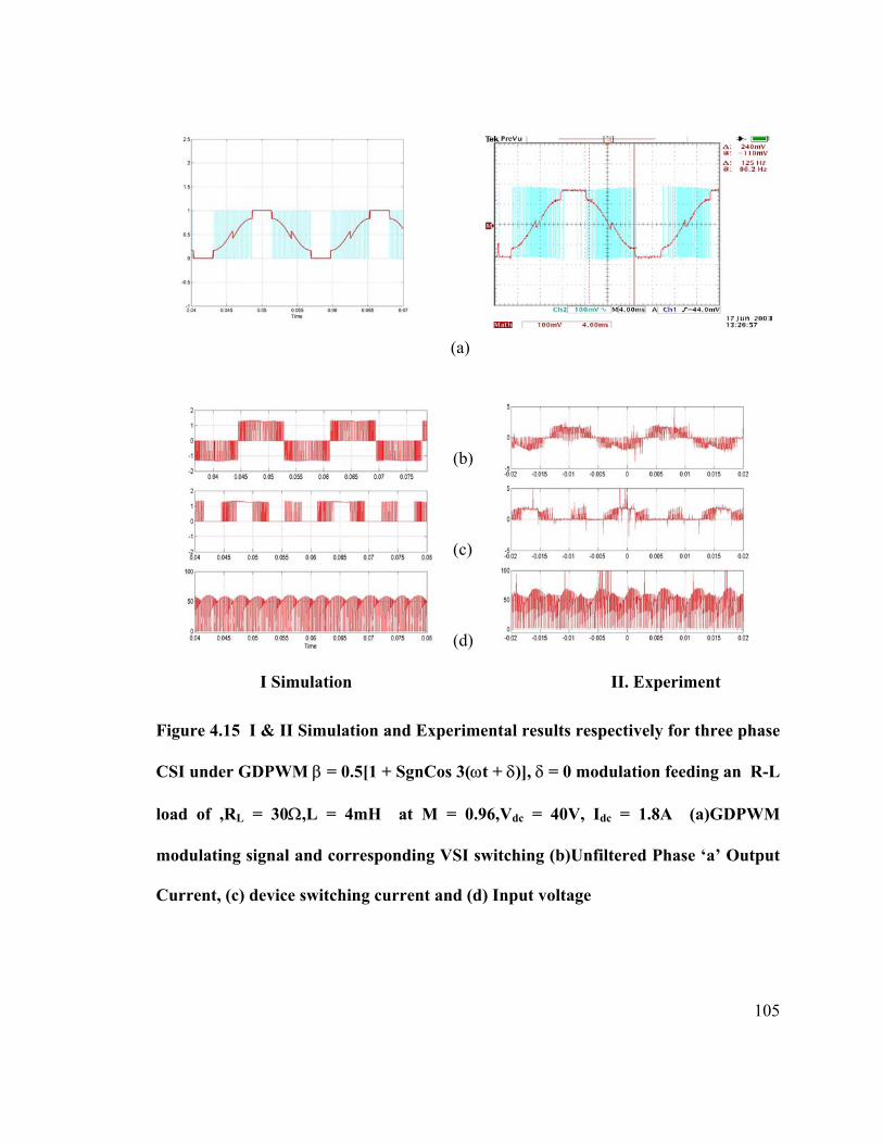
Figure 4.15 I & II Simulation and Experimental results respectively for three phase
CSI under GDPWM β = 0.5[1 + SgnCos 3(ωt + δ)], δ = 0 modulation feeding an R-L
load of ,RL = 30Ω,L = 4mH at M = 0.96,Vdc = 40V, Idc = 1.8A (a)GDPWM
modulating signal and corresponding VSI switching (b)Unfiltered Phase ‘a’ Output
Current, (c) device switching current and (d) Input voltage

106
(a)
(b)
I Simulation II. Experiment
Figure 4.16 I & II Simulation and Experimental results respectively for three phase
CSI under GDPWM β = 0.5[1 + SgnCos 3(ωt + δ)], δ = 0 modulation feeding an R-L
load of ,RL = 30Ω,L = 4mH at M = 0.96,Vdc = 40V, Idc = 1.8A (a) Phase ‘a’ Filtered
Out put Current and (b) Voltage e
Figure 4.17 FFT of the filtered output voltage and current for the above GDPWM
modulating signal β = 0.5[1 + SgnCos 3(ωt + δ)], δ=0 and M = 0.96

107
(a)
(b)
(c)
(d)
I Simulation II. Experiment
Figure 4.18 I&II Simulation and Experimental results respectively for three phase
CSI under GDPWM β = 0.5[1 + SgnCos 3(ωt + δ)], δ = -30 modulation feeding an
R-L load of ,RL = 30Ω,L = 4mH at M = 0.96,Vdc = 40V, Idc = 1.8A (a)GDPWM
modulating signal and corresponding VSI switching (b)Unfiltered Phase ‘a’ Output
Current, (c) device switching current and (d) Input voltage
108
(a)
(b)
I Simulation II. Experiment
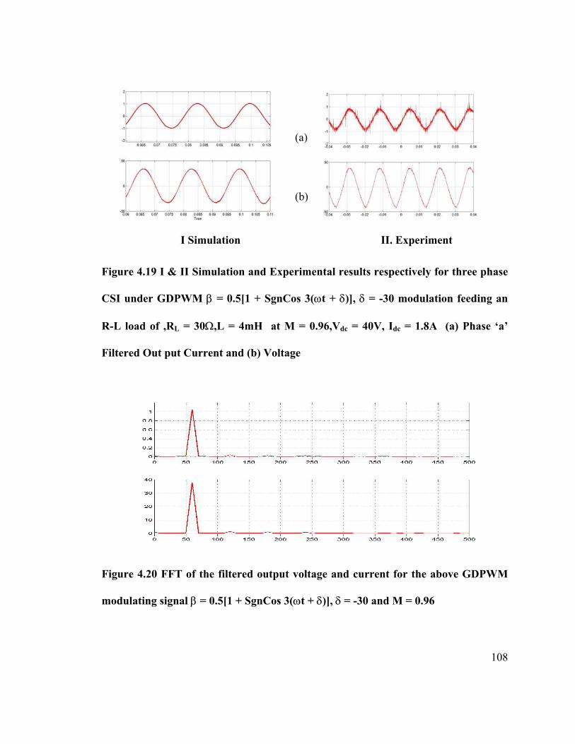
Figure 4.19 I & II Simulation and Experimental results respectively for three phase
CSI under GDPWM β = 0.5[1 + SgnCos 3(ωt + δ)], δ = -30 modulation feeding an
R-L load of ,RL = 30Ω,L = 4mH at M = 0.96,Vdc = 40V, Idc = 1.8A (a) Phase ‘a’
Filtered Out put Current and (b) Voltage
Figure 4.20 FFT of the filtered output voltage and current for the above GDPWM
modulating signal β = 0.5[1 + SgnCos 3(ωt + δ)], δ = -30 and M = 0.96
109
(a)
(b)
(c)
(d)
I Simulation II. Experiment
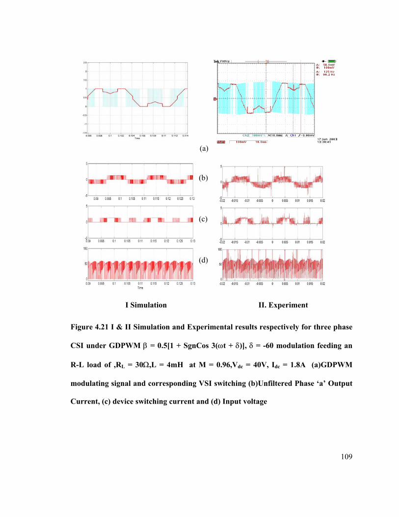
Figure 4.21 I & II Simulation and Experimental results respectively for three phase
CSI under GDPWM β = 0.5[1 + SgnCos 3(ωt + δ)], δ = -60 modulation feeding an
R-L load of ,RL = 30Ω,L = 4mH at M = 0.96,Vdc = 40V, Idc = 1.8A (a)GDPWM
modulating signal and corresponding VSI switching (b)Unfiltered Phase ‘a’ Output
Current, (c) device switching current and (d) Input voltage

110
(a)
(b)
I Simulation II. Experiment
Figure 4.22 I & II Simulation and Experimental results respectively for three phase
CSI under GDPWM β = 0.5[1 + SgnCos 3(ωt + δ)], δ=-60 modulation feeding an R-
L load of ,RL = 30Ω,L = 4mH at M = 0.96,Vdc = 40V, Idc = 1.8A (a)Phase ‘a’
Filtered Out put Current and (b) Voltage
Figure 4.23 FFT of the filtered output voltage and current for the above GDPWM
modulating signal β = 0.5[1 + SgnCos 3(ωt + δ)], δ = -60 and M = 0.96

111
(a)
(b)
(c)
(d)
I Simulation II. Experiment
Figure 4.24 I & II Simulation and Experimental results respectively for three phase
CSI under GDPWM β = 0 modulation feeding an R-L load of ,RL = 30Ω,L = 4mH
at M = 0.96,Vdc = 40V, Idc = 1.8A (a)GDPWM modulating signal and corresponding
VSI switching (b)Unfiltered Phase ‘a’ Output Current, (c) device switching current
and (d) Input voltage

112
(a)
(b)
I Simulation II. Experiment
Figure 4.25 I & II Simulation and Experimental results respectively for three phase
CSI under GDPWM β = 0 modulation feeding an R-L load of ,RL = 30Ω,L = 4mH
at M = 0.96,Vdc = 40V, Idc = 1.8A (a) Phase ‘a’ Filtered Out put Current and (b)
Voltage
Figure 4.26 FFT of the filtered output voltage and current for the above GDPWM
modulating signal β = 0 and M = 1.5

113
(a)
(b)
(c)
(d)
I Simulation II. Experiment
Figure 4.27 I & II Simulation and Experimental results respectively for three phase
CSI under GDPWM β = 0.5 modulation feeding an R-L load of ,RL = 30Ω,L = 4mH
at M = 0.96,Vdc = 40V, Idc = 1.8A (a)GDPWM modulating signal and corresponding
VSI switching (b)Unfiltered Phase ‘a’ Output Current, (c) device switching current
and (d) Input voltage

114
(a)
(b)
I Simulation II. Experiment
Figure 4.28 I & II Simulation and Experimental results respectively for three phase
CSI under GDPWM β = 0.5 modulation feeding an R-L load of ,RL = 30Ω,L = 4mH
at M = 0.96,Vdc = 40V, Idc = 1.8A (a)Phase ‘a’ Filtered Out put Current and (b)
Voltage
Figure 4.29 FFT of the filtered output voltage and current for the above GDPWM
modulating signal β = 0.5 and M = 1.5

115
(a)
(b)
(c)
(d)
I Simulation II. Experiment
Figure 4.30 I & II Simulation and Experimental results respectively for three phase
CSI under GDPWM β = 0.5[1 + SgnCos 3(ωt + δ)], δ = 0 modulation feeding an R-L
load of ,RL = 30Ω,L = 4mH at M = 0.96,Vdc = 40V, Idc = 1.8A (a)GDPWM
modulating signal and corresponding VSI switching (b)Unfiltered Phase ‘a’ Output
Current, (c) device switching current and (d) Input voltage

116
(a)
(b)
I Simulation II. Experiment
Figure 4.31 I & II Simulation and Experimental results respectively for three phase
CSI under GDPWM β = 0.5[1 + SgnCos 3(ωt + δ)], δ = 0 modulation feeding an R-L
load of ,RL = 30Ω,L = 4mH at M = 0.96,Vdc = 40V, Idc = 1.8A (a) Phase ‘a’ Filtered
Out put Current and (b) Voltage
Figure 4.32 FFT of the filtered output voltage and current for the above GDPWM
modulating signal β = 0.5 and M = 1.5

117
(a)
(b)
(c)
(d)
I Simulation II. Experiment
Figure 4.33 I & II Simulation and Experimental results respectively for three phase
CSI under GDPWM β = 0.5[1 + SgnCos 3(ωt + δ)], δ = -30 modulation feeding an
R-L load of ,RL = 30Ω,L = 4mH at M = 0.96,Vdc = 40V, Idc = 1.8A (a) GDPWM
modulating signal and corresponding VSI switching (b)Unfiltered Phase ‘a’ Output
Current, (c) device switching current and (d) Input voltage

118
I Simulation II. Experiment
Figure 4.34 I & II Simulation and Experimental results respectively for
three phase CSI under GDPWM β = 0.5[1 + SgnCos 3(ωt + δ)], δ=-30 modulation
feeding an R-L load of ,RL = 30Ω,L = 4mH at M = 0.96,Vdc = 40V, Idc = 1.8A (a)
Phase ‘a’ Filtered Out put Current and (b) Voltage
Figure 4.35 FFT of the filtered output voltage and current for the above GDPWM
modulating signal β = 0.5[1 + SgnCos 3(ωt + δ)], δ=-30 and M = 1.5
(b)
(a)

119
(a)
(b)
(c)
(d)
I Simulation II. Experiment
Figure 4.36 I & II Simulation and Experimental results respectively for three phase
CSI under GDPWM β = 0.5[1 + SgnCos 3(ωt + δ)], δ = -60 modulation feeding an
R-L load of ,RL = 30Ω,L = 4mH at M = 0.96,Vdc = 40V, Idc = 1.8A (a) GDPWM
modulating signal and corresponding VSI switching (b)Unfiltered Phase ‘a’ Output
Current, (c) device switching current and (d) Input voltage

120
(a)
(b)
I Simulation II. Experiment
Figure 4.37 I & II Simulation and Experimental results respectively for three phase
CSI under GDPWM β = 0.5[1 + SgnCos 3(ωt + δ)], δ=-60 modulation feeding an R-
L load of ,RL = 30Ω,L = 4mH at M = 0.96,Vdc = 40V, Idc = 1.8A (a) Phase ‘a’
Filtered Out put Current and (b) Voltage
Figure 4.38 FFT of the filtered output voltage and current for the above GDPWM
modulating signal β = 0.5[1 + SgnCos 3(ωt + δ)], δ=-60o and M = 1.5

121
1al=0 al=0.5 del=0 del=-30 del=-60
0
0.005
0.01
0.015
0.02
0.025
0.03
0.035
al=0al=0.5del=0del=-30del=-60
Figure 4.39 (a) Comparison of 3rd harmonic obtained from FFT of output currents
for various modulating schemes at ‘m’=0.96
1al=0 al=0.5 del=0 del=-30 del=-60
0
0.001
0.002
0.003
0.004
0.005
0.006
al=0
al=0.5
del=0
del=-30
del=-60
Figure 4.39 (b) Comparison of 5th harmonic obtained from FFT of output currents
for various modulating schemes at ‘m’=0.96

122
1al=0 al=0.5 del=0 del=-30 del=-60
0
0.002
0.004
0.006
0.008
0.01
0.012
0.014
al=0
al=0.5
del=0
del=-30
del=-60
Figure 4.40 (a) Comparison of 3rd harmonic obtained from FFT of output currents
for various modulating schemes at over modulation
1al=0 al=0.5 del=0 del=-30 del=-60
0
0.01
0.02
0.03
0.04
0.05
0.06
al=0
al=0.5
del=0
del=-30
del=-60
Figure 4.40 (b) Comparison of 5th harmonic obtained from FFT of output currents
for various modulating schemes at over modulation

123
1al=0 al=0.5 del=0 del=-30 del=-60
0
0.2
0.4
0.6
0.8
1
1.2
1.4
1.6
al=0
al=0.5
del=0
del=-30
del=-60
Figure 4.41 (a) Comparison of 3rd harmonic obtained from FFT of output voltages
for various modulating schemes at ‘m’ = 0.96
1al=0 al=0.5 del=0 del=-30 del=-60
0
0.2
0.4
0.6
0.8
1
1.2
1.4
al=0
al=0.5
del=0
del=-30
del=-60
Figure 4.41 (b) Comparison of 5th harmonic obtained from FFT of output voltages
for various modulating schemes at ‘m’ = 0.96

124
1al=0 al=0.5 del=0 del=-30 del=-60
0
0.1
0.2
0.3
0.4
0.5
0.6
al=0
al=0.5
del=0
del=-30
del=-60
Figure 4.42 (a) Comparison of 3rd harmonic obtained from FFT of output voltages
for various modulating schemes at over modulation
1al=0 al=0.5 del=0 del=-30 del=-60
0
0.5
1
1.5
2
2.5
al=0
al=0.5
del=0
del=-30
del=-60
Figure 4.42 (b) Comparison of 5th harmonic obtained from FFT of output voltages
for various modulating schemes at over modulation

125
Related Documents