Chapter 4 Algorithmic State Machines and Finite State Machines In this Chapter, we will introduce Algorithmic state machines and consider their use for description of the behavior of control units. Next, we will use algorithmic state machines to design Finite State Machines (FSM) with hardly any constraints on the number of inputs, outputs and states. 4.1 Flowcharts and Algorithmic state machines 4.1.1 Example of ASM. An Algorithmic state machine (ASM) is the directed connected graph containing an initial vertex (Begin), a final vertex (End) and a finite set of operator and conditional vertices (Fig. 1). The final, operator and conditional vertices have only one input, the initial vertex has no input. Initial and operator vertices have only one output, a conditional vertex has two outputs marked by "1" and "0". A final vertex has no outputs. Figure 1. Vertices of Algorithmic state machine As the first example, let us consider a very simple Traffic Light Controller (TLC) presented in the flowchart in Fig. 2. This controller is at the intersection of a main road and a secondary road. Immediately after vertex Begin we have a waiting vertex (one of the outputs of this vertex is connected to its input) with a logical condition Start. It means that the controller begins to work only when signal Start = 1. At this time, cars can move along the main road for two minutes. For that, the traffic light at the main road is green, the traffic light at the secondary road is red and the special timer that counts seconds is set to zero (main_grn := 1; sec_red := 1; t := 0). Although our TLC is very simple it is also a little smart – it can recognize an ambulance on the road. When an ambulance is on the road the signal amb is equal to one (amb = 1), when there is no ambulance on the road this signal is equal to zero (amb = 0). First we will discuss the case when there are no ambulances on the road. Thus, when amb = 0 and t = 120 sec TLC transits into some intermediate state to allow cars to finish driving along the main road: main_yel := 1; sec_red := 1; t := 0. TLC is in this state only for three seconds (t = 3 sec), after which cars can move along the secondary road for 30 seconds: main_red := 1; sec_grn := 1; t := 0. Thirty seconds later, if there are no ambulances on the road (amb = 0; t = 30 sec), there is one more intermediate state. Now cars must finish driving along the secondary road: main_red := 1; sec_yel := 1; t := 0. After three seconds, if, once again, there are no ambulances on the road, the process reaches vertex End, or, that is the same, it returns to the beginning vertex Begin. When there is ambulance on the road (amb = 1) outputs of conditional vertices with logical condition amb, marked by “1” bring us to the intermediate state to let cars to finish their driving: main_yel := 1; sec_yel := 1; t := 0. One more logical condition dmain tells us where the ambulance is – whether it is on the main road or on the secondary one. If it is on the main road (dmain = 1), after three seconds the traffic

Welcome message from author
This document is posted to help you gain knowledge. Please leave a comment to let me know what you think about it! Share it to your friends and learn new things together.
Transcript

Chapter 4 Algorithmic State Machines and Finite State Machines
In this Chapter, we will introduce Algorithmic state machines and consider their use for description of the behavior of control units. Next, we will use algorithmic state machines to design Finite State Machines (FSM) with hardly any constraints on the number of inputs, outputs and states.
4.1 Flowcharts and Algorithmic state machines 4.1.1 Example of ASM. An Algorithmic state machine (ASM) is the directed connected graph containing an initial vertex (Begin), a final vertex (End) and a finite set of operator and conditional vertices (Fig. 1). The final, operator and conditional vertices have only one input, the initial vertex has no input. Initial and operator vertices have only one output, a conditional vertex has two outputs marked by "1" and "0". A final vertex has no outputs.
Figure 1. Vertices of Algorithmic state machine
As the first example, let us consider a very simple Traffic Light Controller (TLC) presented in the flowchart in Fig. 2. This controller is at the intersection of a main road and a secondary road. Immediately after vertex Begin we have a waiting vertex (one of the outputs of this vertex is connected to its input) with a logical condition Start. It means that the controller begins to work only when signal Start = 1. At this time, cars can move along the main road for two minutes. For that, the traffic light at the main road is green, the traffic light at the secondary road is red and the special timer that counts seconds is set to zero (main_grn := 1; sec_red := 1; t := 0). Although our TLC is very simple it is also a little smart – it can recognize an ambulance on the road. When an ambulance is on the road the signal amb is equal to one (amb = 1), when there is no ambulance on the road this signal is equal to zero (amb = 0). First we will discuss the case when there are no ambulances on the road. Thus, when amb = 0 and t = 120 sec TLC transits into some intermediate state to allow cars to finish driving along the main road: main_yel := 1; sec_red := 1; t := 0. TLC is in this state only for three seconds (t = 3 sec), after which cars can move along the secondary road for 30 seconds: main_red := 1; sec_grn := 1; t := 0. Thirty seconds later, if there are no ambulances on the road (amb = 0; t = 30 sec), there is one more intermediate state. Now cars must finish driving along the secondary road: main_red := 1; sec_yel := 1; t := 0. After three seconds, if, once again, there are no ambulances on the road, the process reaches vertex End, or, that is the same, it returns to the beginning vertex Begin. When there is ambulance on the road (amb = 1) outputs of conditional vertices with logical condition amb, marked by “1” bring us to the intermediate state to let cars to finish their driving: main_yel := 1; sec_yel := 1; t := 0. One more logical condition dmain tells us where the ambulance is – whether it is on the main road or on the secondary one. If it is on the main road (dmain = 1), after three seconds the traffic

66 – Logic and System Design
light will be green on the main road, otherwise (dmain = 0) the traffic light will be green on the secondary road.
Figure 2. A simple Traffic Light Controller
In the flowchart, a logical condition is written in each conditional vertex. It is possible to write the same logical condition in different conditional vertices. A microinstruction (an operator), containing one, two, three or more microoperations, is written in each operator vertex of the flowchart. It is possible to write the same operator in different operator vertices.
If we replace logical conditions by x1, x2, … , xL, microoperations by y1, y2, … , yN and operators by Y1, Y2, … , YT we will get Algorithmic State Machine (ASM). ASM for the flowchart in Fig. 2 is shown in Fig. 3. ASM vertices are connected in such a way that:
1. Inputs and outputs of the vertices are connected by arcs directed from an output to an input, each output is connected with only one input;
2. Each input is connected with at least one output; 3. Each vertex is located on at least one of the paths from vertex “Begin” to
vertex “End”. Hereinafter we will not consider ASMs with subgraphs, containing an infinite cycle. An example of such a subgraph with an infinite

Chapter 4 Algorithmic state machines and finite state machines – 67
loop between vertices with Y1 and Y3 is shown in Fig. 4. The dots in this ASM between vertex “Begin” and the conditional vertex with x1 and between this vertex and vertex “End” mean that ASM has other vertices on the path from vertex “Begin” to vertex “End”. The vertices in the loop are not on the path from “Begin” to “End”.
4. One of the outputs of a conditional vertex can be connected with its input. We will call such conditional vertices the “waiting vertices”, since they simulate the waiting process in the system behavior description.
Figure 3. ASM for the flowchart in Fig. 2
Begin
Endx1
. .
.
1 . . .
Y1
0
x3 01
x2 Y21Y3 0 Figure 4. Subgraph with an infinite loop

68 – Logic and System Design
One more example of ASM G1 with logical conditions X = {x1, …, x7} and microoperations Y = {y1, …, y10} is shown in Fig. 5. This ASM has eight operators Y1, …, Y8, they are written near operator vertices. 4.1.2 Transition functions. Let us discuss the paths between the vertex “Begin”, the vertex “End” and operator vertices passing only through conditional vertices. We will write such paths as follows:
jiRii YxxY ~...~1 (1)
In such a path, irx~ is equal to irx if the path proceeds from the conditional vertex
with irx via output ‘1’, and irx~ is equal to 'irx if the path proceeds from the
conditional vertex with irx via output ‘0’. For example, we have the following paths from Yb (vertex Begin) in ASM G1:
Yb x'1 Y2; Yb x1x2x'3 Y6; Yb x1x'2 Y1; Yb x1x2x3 Y5.
Begin
1
x3
1
y1 y3
1
y1 y2 0
x4
x2
x1
y40
x5
y5 y6 y7
1
x6
x7
0
0
End
x1
10
y8 y91
1y3 y4
0
x6
y6 y7
10
y6 y70
0
Yb
Y6
Y1
Y5
Y7
Y4
y3 y6 y101 Y8
Y3
Y2
Ye
Y6
Figure 5. ASM G1
Let us match a product of variables in the path (1) from operator vertex Yi to operator vertex Yj
iRiij xx ~...~1=α
with this path from Yi to Yj. For example, for ASM G1 in Fig. 5
α17 = x4 x'1; α12 = x'4; α14 = x4 x1. If there exist H paths between Yi and Yj through the conditional vertices, then

Chapter 4 Algorithmic state machines and finite state machines – 69
αij = α1ij + α2ij + … + αHij where αhij (h = 1, …,H) is the product for the h-th path. Let us call αij a transition function from operator (microinstruction) Yi to operator (microinstruction) Yj. Note that for the path Y6Y7 (operator Y7 follows operator Y6 immediately without conditional vertices) α67 = 1, as the product of an empty set of variables is equal to one. 4.1.3 Value of ASM at the sequence of vectors. Denote all possible L-component vectors of the logical conditions x1, …,xL by ∆1, …,∆2L and define the execution of an ASM on any given sequence of vectors ∆1, …,∆mq beginning from the initial operator Yb. We will demonstrate this procedure by means of ASM G1 in Fig. 5 and the sequence (2) containing eight vectors ∆1, …,∆8:
ASM G1 in Fig. 5 contains logical variables x1,…,x7 and operators Yb ,Y1, …,Y8,Ye. Now let us find the sequence of operators which would be implemented, if we consecutively, beginning from Yb, give variables the values from these vectors. We suppose that the values of logical conditions can be changed only during an execution of operators. Step 1. Write the initial operator
Yb. Step 2. Let logical variables x1,…,x7 take their values from vector ∆1. From the set of the transition functions αb1,…, αb8, αbe we choose such a function αbt that αbt(∆1) = 1. In our example for the operator Yb, the following transition functions are not identically equal to zero:
αb5 = x1 x2 x3; αb6 = x1 x2 x'3; αb1 = x1 x'2; αb2 = x'1. We will call such functions non-trivial transition functions to distinguish them from the trivial functions, which are identically equal to zero. Function αij is trivial if there is no path from operator Yi to operator Yj. In the example at this step, we choose the function αb1, since only αb1 is equal to one on the first vector ∆1:
αb1 (∆1) = 1. Write Y1 to the right of Yb:
YbY1.
x1 x2 x3 x4 x5 x6 x7
∆1 = 1 0 1 0 1 1 1 ∆2 = 0 1 1 0 1 0 0 ∆3 = 1 0 1 0 0 1 0 ∆4 = 0 1 0 0 0 0 1 (2) ∆5 = 1 1 0 1 1 1 0 ∆6 = 1 1 0 0 1 0 1 ∆7 = 0 1 1 1 0 0 0 ∆8 = 0 1 0 1 0 0 1

70 – Logic and System Design
Step 3. Let x1,…,x7 take their values from vector ∆2. From the set of the transition functions α11,…, α18, α1e we choose non-trivial functions
α14 = x4 x1; α17 = x4 x'1; α12 = x'4 and among them – the only function α12 (∆2) = 1. Write Y2 to the right of YbY1:
YbY1Y2.
The computational process for the given sequence of vectors may reach its end in two cases:
1. The final vertex “End” is reached. In this case, the last operator is Ye. The number of operators in the operator row (without Yb and Ye) is less or equal (if we reached the final vertex with the last vector) to the number of vectors;
2. The vectors are exhausted but we have not yet reached the final vertex. In this case, the number of operators in the operator row is equal to the number of vectors.
In our example, we reached the final vertex “End” at the seventh vector
∆7 = 0 1 1 1 0 0 0
and we get the row Yb Y1 Y2 Y4 Y2 Y3 Y8 Ye. (3)
The operator row thus obtained is the value of the ASM G1 for the given sequence of vectors (2).
4.2 Synthesis of Mealy FSM
We will use Algorithmic state machines to describe the behavior of digital systems, mainly of their control units. But if we must construct a logic circuit of the control unit we should use a Finite state machine (FSM). We will consider methods of synthesis of FSM Mealy, Moore and their combined model implementing a given ASM, with hardly any constrains on the number of inputs, outputs and states. 4.2.1 Construction of a marked ASM. As an example we will use ASM G1 in Fig. 6. A Mealy FSM implementing given ASM may be constructed in two stages: Stage1. Construction of a marked ASM; Stage 2. Construction of a state diagram (state graph). At the first stage, the inputs of vertices following operator vertices are marked by symbols a1, a2, …, aM as follows:
1. Symbol a1 marks the input of the vertex following the initial vertex “Begin” and the input of the final vertex “End”;
2. Symbols a2, …, aM mark the inputs of all vertices following operator vertices; 3. Vertex inputs are marked only once; 4. Inputs of different vertices, except the final one, are marked by different
symbols.
Marked ASM G1 in Fig. 6 is a result of the first step. Symbols a1, …, a6 are used to mark this ASM. Note, that we mark the inputs not only of conditional vertices but of operator vertices as well (see mark a3 at the input of the vertex with operator Y7). It is important that each marked vertex follows an operator vertex.
Chapter 4 Algorithmic state machines and finite state machines – 71
Figure 6. ASM G1 marked for the Mealy FSM synthesis
4.2.2 Transition Paths. At the second stage, we will consider the following paths in the marked ASM: sgmmRmm aYxxa ~...~
1 (P1) 11
~...~ axxa mmRmm (P2) We call these paths transition paths. Thus, the path P1 proceeds from am to as (am = as
is also allowed) and contains only one operator vertex at the end of this path. The path P2 proceeds from am only to a1 without operator vertex. Here, mrmr xx =~ , if on
the transition path we leave the conditional vertex with mrx via output ‘1’ and
mrmr xx '~ = if we leave it via output ‘0’. If Rm = 0 on the path P1, two operator vertices follow one after another and this path turns into
sgm aYa . There are sixteen transition paths in the marked ASM G2 in Fig. 6: Note, that the path a2 x4x'1 a3 doesn’t correspond to the transition path P1 (the operator vertex is absent on the path) and to transition path P2 (it isn’t a path to a1). Thus, it isn’t a transition path and we should go on to get the path a2 x4x'1 Y7 a6. For the same reason, paths a4 x'5x'1 a3 and a6 x'6 a3 are not the transition paths either.
a1 x1x2x3 Y5 a2
a1 x1x2x'3 Y6 a3
a1 x1x'2 Y1 a2
a1 x'1 Y2 a4
a2 x4x1 Y4 a2
a2 x4x'1 Y7 a6
a2 x'4 Y2 a4
a3 Y7 a6
a4 x5 Y3 a5
a4 x'5x1 Y4 a2
a4 x'5x'1 Y7 a6
a5 x6 Y4 a2
a5 x'6x7 Y8 a1
a5 x'6x'7 a1
a6 x6 Y6 a1
a6 x'6 Y7 a6

72 – Logic and System Design
4.2.3 Graph of FSM. Next we construct a graph (state diagram) of FSM Mealy with states (marks) a1, …, aM, obtained at the first stage. We have six such states a1, …, a6 in our example. Thus, the FSM graph contains as many states as the number of marks we get at the previous stage. Now we should define transitions between these states. FSM has a transition from state am to state as with input X(am, as) and output Yg (see the upper subgraph in Fig. 7) if, in ASM, there is transition path P1
sgmRmm aYxxam
~...~1 .
Here X(am, as) is the product of logical conditions written in this path: X(am, as) = mmRm xx ~...~
1 .
In exactly the same way, for the path sgm aYa we have a transition from state am to state as with input X(am, as) = 1 and output Yg, as the product of an empty set of variables is equal to zero. If, for a certain r (r = 1, …, Rm), symbol xmr (or x'mr) occurs several times on the transition path, all symbols xmr (x'mr) but one are deleted; if for a certain r (r = 1, …, Rm), both symbols xmr and x'mr occur on the transition path, this path is removed. In such a case X(am, as) = 0. For the second transition path P2, FSM transits from state am to the initial state a1 with input X(am, a1) and output Y0 (see the lower subgraph in Fig. 7). Y0 is the operator containing an empty set of microoperations.
Figure 7. Subgraphs for transition paths P1 and P2
As a result, we obtain a Mealy FSM with as many states as the number of marks we used to mark the ASM in Fig. 6. The state diagram of the Mealy FSM is shown in Fig. 8.
Figure 8. The state diagram of the Mealy FSM
4.2.4 How not to loose transition paths. Sometimes, if ASM contains many conditional vertices, it is difficult not to loose one or several transition paths. Here

Chapter 4 Algorithmic state machines and finite state machines – 73
we give a very simple algorithm to resolve this problem. This algorithm has only two steps.
1. Find the first transition path leaving each conditional vertex through output
'1'. For subgraph of ASM in Fig. 9 we will get the following first path from state a2:
a2 x1 x2 x5 Y6 a3.
2. Invert the last non-inverted variable in the previous path, return to ASM and continue the path (if it is possible) leaving each conditional vertex through output '1'. To construct the second path, we should invert variable x5. We cannot continue because we reached an operator vertex:
a2 x1 x2 x'5 Y2 a3.
We should construct paths in the same manner until all variables in a transition path will be inverted. For our example, we will get the following paths:
Figure 9. Subgraph of ASM
4.2.5 Transition tables of Mealy FSM. The graph of Mealy FSM in Fig. 8 has only 6 states and 16 arcs. Practically, however, we must construct FSMs with tens of states and more than one-two hundreds of transitions. In such a case, it is difficult to use a graph, so we will present it as a table. Table 1 for the same Mealy FSM has five columns:
• am – a current state; • as – a next state; • X(am,as) – an input signal; • Y(am,as) – an output signal; • H – a number of line.
a2 x1 x'2 x5 x6 Y3 a4; a2 x1 x'2 x5 x'6 x7 x4 Y5 a5; a2 x1 x'2 x5 x'6 x7 x'4 Y7 a4; a2 x1 x'2 x5 x'6 x'7 Y5 a5;
a2 x1 x'2 x'5 Y2 a3; a2 x'1 x3 x7 x4 Y5 a5; a2 x'1 x3 x7 x'4 Y7 a4; a2 x'1 x3 x'7 Y5 a5;
a2 x'1 x'3 x6 Y3 a4; a2 x'1 x'3 x'6 x7 x4 Y5 a5; a2 x'1 x'3 x'6 x7 x'4 Y7 a4; a2 x'1 x'3 x'6 x'7 Y5 a5.

74 – Logic and System Design
Actually, immediately from ASM, we should write transition paths, one after another, into the transition table. In Table 1, ~xt is used instead of x't for the inversion of xt.
Now we will discuss what kind of FSM we have received. Our ASM G1 in Fig. 6 which we used to construct FSM S1 in Table 1, has seven logical conditions and ten microoperations. FSM S1 has seven binary inputs in the column X(am,as) and ten binary outputs in the column Y(am,as). The input signal of this FSM (Fig. 10) is the 7-component vector, the output signal of this FSM is the 10-component vector.
Table 1. Direct transition table of Mealy FSM S1
Figure 10. FSM as a black box
Let us take one of the rows from Table 1, for example row 3, and look at the behavior of FSM presented in this row. Our FSM transits from state a1 into state a2 when the product x1 x'2 = 1. It is clear that such a transition takes place for any input vector in which the first component is equal to 1, the second component is equal to 0. The values of other components are not important. Thus, we can say that the third row of Table 1 presents transitions from a1 with any vector which is covered by cube 10xxxxx. In other words, this row presents not one but 25 = 32 transitions. In exactly the same way, the first and the second row present 16 transitions, the fourth row – 64 transitions and the eighth row – 128 transitions.
Two microoperations y1, y2, written in the third row of the output column, mean that two components y1 and y2 are equal to 1 and others are equal to 0 (y1= y2 =1; y3 = y4 = … = y10 =0) in the output vector. I remind you that if the operator, written in the operator vertex of some ASM, contains microoperations ym, yn, only these microoperations are equal to 1 and other microoperations are equal to 0 during implementation of this operator.
Let us compare Table 1 with a classical FSM representation in Table 3.7 from Chapter 3. If we would like to present our FSM with six states a1, …, a6 and seven inputs x1, …, x7 in the classical table, this table will have about 6x27 rows, because each row of
am as X(am,as) Y(am,as) H a1 a2
a3
a2
a4
x1x2x3
x1x2~x3
x1~x2
~x1
y1y3
y6y7
y1y2
y4
1 2 3 4
a2 a2
a6
a4
x4x1
x4~x1
~x4
y8y9
y3y4
y4
5 6 7
a3 a6 1 y3y4 8 a4 a5
a2
a6
x5
~x5x1
~x5~x1
y5y6y7
y8y9
y3y4
9 10 11
a5 a2
a1
a1
x6
~x6x7
~x6~x7
y8y9
y3y6y10
-
12 13 14
a6 a1
a6 x6
~x6 y6y7
y3y4 15 16

Chapter 4 Algorithmic state machines and finite state machines – 75
this table describes only one FSM transition. In our Table 1 from this Chapter, we have only 16 rows because each row of such table presents lot of transitions. The specific feature of such FSM is the multiplicity of inputs in the column X(am,as), maybe several tens or even hundreds, but each product in one row contains only few variables from the whole set of input variables – as a rule, not more than 8 – 10 variables. It means that each time the values of the output variables depend only on the values of a small number of the input variables. Really, if, for example, FSM has 30 input variables, the total number of input vectors is equal to 230, and if each time the values of the output variables depended on the values of all the input variables, no designer could either describe or construct such an FSM. Let us briefly discuss the correspondence between FSM S1 (Table 1) and ASM G1 (Fig. 6) which we used to construct FSM S1. In Section 4.1.3 we got the value of ASM G1
Yb Y1 Y2 Y4 Y2 Y3 Y8 Ye for some random sequence of vectors (2) of logical conditions:
Now we will find the response of FSM S1 in the initial state a1 to the same sequence of input vectors: State sequence a1 a2 a4 a2 a4 a5 a1 Input sequence ∆1 ∆2 ∆3 ∆4 ∆5 ∆6 Response y1y2 y4 y8y9 y4 y5y6y7 y3y6y10 (4) Microinstructions Y1 Y2 Y4 Y2 Y3 Y8 Let FSM be in the initial state a1 with the first vector ∆1 = 1010111 at its input. To determine the next state and the output we should find such a row in the array of transitions from a1 (Table 1) that the product X(am,as), written in this row, be equal to one at input vector ∆1. Since x1x′2(∆1) = 1 (the third row), FSM S1 produces output signal y1y2 = Y1 and transits into state a2. Similarly, we find that x′4(∆2) is equal to one at one of transitions from state a2 and FSM transits to the state a4 with the output signal y4 = Y2 (see row 7 in Table 1) etc. As a result, we get the response of FSM S1 in the initial state a1 to the input sequence ∆1, …, ∆6 in the fourth row of sequence (4). As seen from this row, the FSM response is equal to the value of ASM G1 for the same input sequence. Note, that we consider here only the FSM response until its return to the initial state a1 and this response Y1 Y2 Y4 Y2 Y3 Y8 corresponds to the value of ASM G1 between the operator Yb (vertex "Begin") and the operator Ye (vertex "End"). Let us define FSM S as implementing ASM G if the response of this FSM in the state a1
to any input sequence (until its return to the state a1) is equal to the value of ASM G
x1 x2 x3 x4 x5 x6 x7
∆1 = 1 0 1 0 1 1 1 ∆2 = 0 1 1 0 1 0 0 ∆3 = 1 0 1 0 0 1 0 ∆4 = 0 1 0 0 0 0 1 ∆5 = 1 1 0 1 1 1 0
∆6 = 1 1 0 0 1 0 1 ∆7 = 0 1 1 1 0 0 0 ∆8 = 0 1 0 1 0 0 1
76 – Logic and System Design
for the same input sequence. From the considered method of synthesis of Mealy FSM S1 from ASM G1 it follows that this FSM S1 implements ASM G1.
4.2.6 Synthesis of Mealy FSM logic circuit. As in Chapter 3, we will construct a Mealy FSM logic circuit with the structure presented in Fig. 11. To design this circuit we will use an FSM structure table (Table 2). This table was constructed from the direct transition table (Table 1) by adding three additional columns:
• K(am) – a code of the current state; • K(as) – a code of the next state; • D(am,as) – an input memory function.
Figure 11. The structure for the Mealy FSM logic circuit
Table 2. Structure table of FSM S1
am K(am) as K(as) X(am,as) Y(am,as) D(am,as) H a1 001 a2
a3
a2
a4
000 101 000 010
x1x2x3
x1x2~x3
x1~x2
~x1
y1y3
y6y7
y1y2
y4
– d1d3
–
d2
1 2 3 4
a2 000 a2
a6
a4
000 100 010
x4x1
x4~x1
~x4
y8y9
y3y4
y4
– d1
d2
5 6 7
a3 101 a6 100 1 y3y4 d1 8 a4 010 a5
a2
a6
110 000 100
x5
~x5x1
~x5~x1
y5y6y7
y8y9
y3y4
d1d2 –
d1
9 10 11
a5 110 a2
a1
a1
000 001 001
x6
~x6x7
~x6~x7
y8y9
y3y6y10
-
– d3
d3
12 13 14
a6 100 a1
a6 001 100
x6
~x6 y6y7
y3y4 d3
d1 15 16
To encode FSM states we constructed Table 3 where p(as) is the number of appearances of each state in the next state column as in Table 2. The algorithm for state assignment is absolutely the same as in Chapter 3. First, we use the zero code for state a2 with max p(a2) = 5. Then codes with one '1' are used for states a6, a1, a4 with the next max appearances and, finally, two codes with two 'ones' are used for the left states a3 and a5. To fill column D(am,as) it is sufficient to write there column K(as) because the input of D flip-flop is equal to its next state. However, here we use the same notation as in column Y(am,as) and write dr in the column D(am,as) if dr is equal to 1 at the

Chapter 4 Algorithmic state machines and finite state machines – 77
corresponding transition (am,as) – equal to 1 in column K(as). After that, the shaded part of Table 2 is something like a truth table with input variables t1, t2, t3, x1, …, x7 in the columns K(am) and X(am,as) and output variables (functions) y1, …, y10, d1, d2, d3 in the columns Y(am,as) and D(am,as).
Table 3. State assignment
as p(as) t1 t2 t3
a1 3 0 0 1 a2 5 0 0 0 a3 1 1 0 1 a4 2 0 1 0 a5 1 1 1 0 a6 4 1 0 0
Let Am be a product, corresponding to the state code K(am), and Xh be the product of input variables, written in the column X(am,as) in the h row. For example, from the column K(am): K(a1) = 001, then A1 = t'1t'2t3; K(a2) = 000, then A2 = t'1t'2t'3; K(a3) = 101, then A3 = t1t'2t3 etc. Immediately from the column X(am,as) we get:
X1 = x1x2x3; X2 = x1x2x'3; X6 = x4x'1; X8 = 1; X16 = x'6. We call the term
eh = Am Xh
the product corresponding to the h row of the FSM structure table if am is the current state in this row. For example, from Table 2, we get:
e1 = t'1t'2t3 x1x2x3; e2 = t'1t'2t3 x1x2x'3; e6 = t'1t'2t'3 x4x'1; e8 = t1t'2t3; e16 = t1t'2t'3 x'6.
Let H(yn) is the set of rows with yn in the column Y(am,as). Then, as in the truth table:
.)(
∑∈
=nyHh
hn ey
For example, y6 is written in rows 2, 9, 13, 15 in the column Y(am,as). Then
y6 = e2 + e9 + e13 + e15 = t'1t'2t3x1x2x'3 + t'1t2t'3 x5 + t1t2t'3 x'6x7 + t1t'2t'3 x6. In exactly the same way, if H(dr) is the set of rows with dr in the column D(am,as), then
.)(
∑∈
=rdHh
hr ed
For example, d2 is written in rows 4, 7, 9 in the column D(am,as). Then
d2 = e4 + e7 + e9 = t'1t'2t3 x'1+ t'1t'2t'3 x'4 + t'1t2t'3 x5. Thus, immediately from Table 1 we can get expressions for outputs of circuit “Logic” in Fig. 11:
y1 = e1 + e3 = t'1t'2t3 x1x2x3 + t'1t'2t3 x1x'2;
78 – Logic and System Design
y2 = e3 = t'1t'2t3 x1x'2; y3 = e1 + e6 + e8 + e11 + e13 + e16 = t'1t'2t3 x1x2x3 + t'1t'2t'3 x4x'1 + t1t'2t3 + + t'1t2t'3 x'5x'1 + t1t2t'3 x'6x7 + t1t'2t'3 x'6; . . . y10 = e13 = t1t2t'3 x'6x7;
d1 = e2 + e6 + e8 + e9 + e11 + e16 = t'1t'2t3 x1x2x'3 + t'1t'2t'3 x4x'1 + t1t'2t3 + + t'1t2t'3 x5 + t'1t2t'3 x'5x'1 + t1t'2t'3 x'6; d2 = e4 + e7 + e9 = t'1t'2t3 x'1+ t'1t'2t'3 x'4 + t'1t2t'3 x5; d3 = e2 + e13 + e14 + e15 = t'1t'2t3 x1x2x'3 + t1t2t'3 x'6x7 + t1t2t'3 x'6x'7 + t1t'2t'3 x6.
How many different products are there in these expressions? The answer is very simple – only sixteen, because we have 16 rows in Table 2 and only one product corresponds to one row. Thus, we should not write any expressions but can design the logic circuit immediately from the structure table. For that, it is sufficient to construct H AND-gates, one for each row, and N+R OR-gates, one for each output variable yn (n = 1, …, 10 in our example) and one for each input memory function dr (r = 1, 2, 3 in our example). The logic circuit of Mealy FSM is shown in Fig. 12. We have constructed 16 AND-gates, as there are 16 rows in its structure table. The number of OR-gates in this circuit is less than the number of input memory functions and output functions. Really, if yn or dr (y2 and y10 in our example) are written only in one row of the structure table, it is not necessary to construct OR-gate for such yn or dr, we can get these signals from the corresponding AND-gates. Moreover, we have constructed one OR-gate for y8 and y9 since these outputs are always together in the structure table of Mealy FSM S1. 4.2.7 ASM with waiting vertices. In this section, we will show that the algorithm for FSM synthesis does not change if ASM contains waiting vertices. In a waiting vertex, one of its outputs is connected with its input (see the ASM subgraph in Fig. 13). Let us find all transition paths from the state a8. The first two are trivial – see the first two rows in Table 4. To find the next path we should invert the variable x7. The output '0' for x7 brings us to the input of this conditional vertex. So, the next paths will be:
a8 ~x7 x7 x12 (y11) a13; a8 ~x7 x7 ~x12 (y23, y29) a17.
The products of input variables for both of these paths are equal to zero (x'7 x7 = 0), so FSM cannot transit from the state a8 to any other state when x7 = 0. If FSM cannot transit into any other state, it remains in the same state a8 or, we can say, it transits from a8 to a8 with X(a8, a8) = x'7. No output variables are equal to '1' at this transition, so we have '–' in the column Y(am, as) in the third row. The next example (Fig.14) presents a general case. The only difference from the previous example – the waiting vertex is in the middle of the path. After the third path in Table 5 we should invert variable x11 and again return to the input of the conditional vertex with x11. We can construct the following transitions paths:
a10 ~x4 ~x11 x11 x27 (y33) a22; a10 ~x4 ~x11 x11 ~x27 (y7, y31) a17.

Chapter 4 Algorithmic state machines and finite state machines – 79
The products for both of these paths are equal to zero. So, when x4 = 0, we reached a waiting vertex with condition x11. If x11 = 0 (return to the input), FSM transits from state a10 to state a10 (remains in this state) with input x'4 x'11 and each output variable is equal to zero (the forth row in Table 5).
Figure 12. The logic circuit for Mealy FSM S1
1
x12
x7
a8
0
y111
y23 y29
0a13
a17
Figure 13. Subgraph G1 with waiting vertex
Table 4. Transitions for subgraph G1
am as X(am,as) Y(am,as) H . . .
a8 a13
a17
a8
x7x12
x7~x12 ~x7
y11
y23y29
–

80 – Logic and System Design
4.3 Synthesis of Moore FSM
As an example, we will use ASM G1 in Fig. 15. A Moore FSM, implementing given ASM, can be constructed in two stages: Stage 1. Construction of a marked ASM; Stage 2. Construction of an FSM transition table. At the first stage, the vertices "Begin", "End" and operator vertices are marked by symbols a1, a2, …, aM as follows:
1. Vertices "Begin" and "End" are marked by the same symbol a1;
2. Operator vertices are marked by different symbols a2, …, aM;
3. All operator vertices should be marked.
Thus, while synthesizing a Moore FSM, symbols of states do not mark inputs of vertices following the operator vertices (as in the Mealy FSM) but operator vertices themselves. The number of marks is T+1, where T is the number of operator vertices in the marked ASM. In our example (Fig. 15), we need marks a1, …, a10 for ASM G1.
We will find the following transition paths in the marked ASM:
smRmm axxam
~...~1 .
Thus, the transition path is the path between two operator vertices, containing Rm conditional vertices. Here, as above in the case of Mealy FSM, mrmr xx =~ , if in the
transition path, we leave the conditional vertex with mrx via output ‘1’ and mrmr xx '~ =
if we leave the vertex with mrx via output ‘0’. If Rm = 0 in such a path, there are no
conditional vertices between two operator vertices, and this path turns into smaa .
Figure 14. Subgraph G2 with a waiting vertex
Table 5. Transitions for subgraph G2
am as X(am,as) Y(am,as) H . . .
a10 a16
a22
a17
a10
x4
~x4x11x27
~x4x11~x27
~x4~x11
y15y27
y33
y7y31
–

Chapter 4 Algorithmic state machines and finite state machines – 81
Figure 15. ASM G1 marked for the Moore FSM synthesis
At the second stage we construct a transition table (or the state diagram) of the Moore FSM with states (marks) a1, …, aM, obtained at the first stage. We have ten such states a1, …, a10 in our example. Thus, the FSM contains as many states as the number of marks we get at the previous stage. Now we should define transitions between these states. Thus, a Moore FSM has a transition from state am to state as with input X(am, as) (see
the upper subgraph in Fig. 16) if, in ASM, there is a transition path smRmm axxam
~...~1 .
Here X(am, as) is a product of logical conditions written in this path: X(am, as) =
mmRm xx ~...~1 . In exactly the same way, for the path smaa (see the lower subgraph in Fig.
16) we have a transition from state am to state as with input X(am, as) = 1, because the product of an empty set of variables is equal to zero. If am marks the operator vertex with operator Yt, then λ(am) = Yt, i.e. we identify the operator Yt written in the operator vertex with this state am.
Figure 16. Subgraphs to illustrate transitions in the Moore FSM
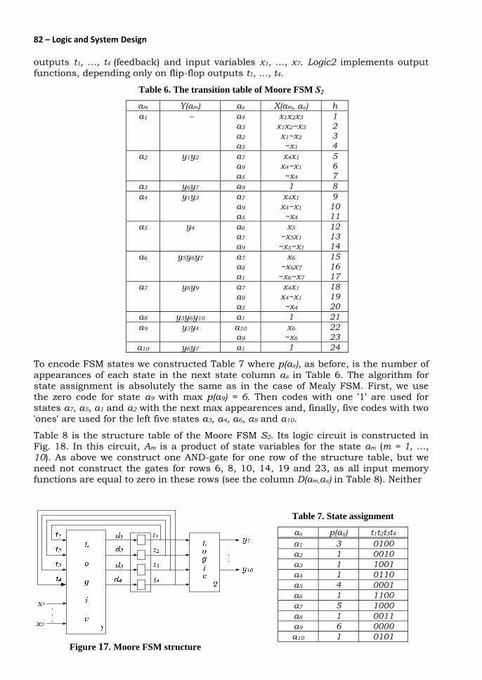
The transition table for Moore FSM S2, thus constructed, is presented in Table 6. The outputs are written in column Y(am) immediately after the column with the current states. To design the logic circuit for this FSM we will use the structure presented in Fig. 17. It consists of two logic blocks (Logic1 and Logic2) and memory block with four D flip-flops. Logic1 implements input memory functions, depending on flip-flop
82 – Logic and System Design
outputs t1, …, t4 (feedback) and input variables x1, …, x7. Logic2 implements output functions, depending only on flip-flop outputs t1, …, t4.
Table 6. The transition table of Moore FSM S2
am Y(am) as X(am, as) h a1 – a4
a3
a2
a5
x1x2x3
x1x2~x3
x1~x2
~x1
1 2 3 4
a2 y1y2 a7
a9
a5
x4x1
x4~x1
~x4
5 6 7
a3 y6y7 a9 1 8 a4 y1y3 a7
a9
a5
x4x1
x4~x1
~x4
9 10 11
a5 y4 a6
a7
a9
x5
~x5x1
~x5~x1
12 13 14
a6 y5y6y7 a7
a8
a1
x6
~x6x7
~x6~x7
15 16 17
a7 y8y9 a7
a9
a5
x4x1
x4~x1
~x4
18 19 20
a8 y3y6y10 a1 1 21 a9 y3y4 a10
a9 x6
~x6 22 23
a10 y6y7 a1 1 24
To encode FSM states we constructed Table 7 where p(as), as before, is the number of appearances of each state in the next state column as in Table 6. The algorithm for state assignment is absolutely the same as in the case of Mealy FSM. First, we use the zero code for state a9 with max p(a9) = 6. Then codes with one '1' are used for states a7, a5, a1 and a2 with the next max appearences and, finally, five codes with two 'ones' are used for the left five states a3, a4, a6, a8 and a10.
Table 8 is the structure table of the Moore FSM S2. Its logic circuit is constructed in Fig. 18. In this circuit, Am is a product of state variables for the state am (m = 1, …, 10). As above we construct one AND-gate for one row of the structure table, but we need not construct the gates for rows 6, 8, 10, 14, 19 and 23, as all input memory functions are equal to zero in these rows (see the column D(am,as) in Table 8). Neither
Figure 17. Moore FSM structure
Table 7. State assignment
as p(as) t1t2t3t4 a1 3 0100 a2 1 0010 a3 1 1001 a4 1 0110 a5 4 0001 a6 1 1100 a7 5 1000 a8 1 0011 a9 6 0000 a10 1 0101

Chapter 4 Algorithmic state machines and finite state machines – 83
Table 8. The structure table of the Moore FSM S2
am Y(am) K(am) as K(as) X(am,as) D(am,as) h a1 – 0100 a4
a3
a2
a5
0110 1001 0010 0001
x1x2x3
x1x2~x3
x1~x2
~x1
d2d3
d1d4
d3
d4
1 2 3 4
a2 y1y2 0010 a7
a9
a5
1000 0000 0001
x4x1
x4~x1
~x4
d1
–
d4
5 6 7
a3 y6y7 1001 a9 0000 1 – 8 a4 y1y3 0110 a7
a9
a5
1000 0000 0001
x4x1
x4~x1
~x4
d1
–
d4
9 10 11
a5 y4 0001 a6
a7
a9
1100 1000 0000
x5
~x5x1
~x5~x1
d1d2
d1
–
12 13 14
a6 y5y6y7 1100 a7
a8
a1
1000 0100 0011
x6
~x6x7
~x6~x7
d1
d2
d3d4
15 16 17
a7 y8y9 1000 a7
a9
a5
1000 0000 0001
x4x1
x4~x1
~x4
d1
–
d4
18 19 20
a8 y3y6y10 0011 a1 0100 1 d2 21 a9 y3y4 0000 a10
a9 0101 0000
x6
~x6 d2d4
– 22 23
a10 y6y7 0101 a1 0100 1 d2 24
x3x2x1A1
x3x2x1A1
x2x1A1
x1A1
x7x6A6
x4x1A7
x4A7
x6A9
A8
A10
A10
A9
A8
A3
A2
A1
1DC1
1DC1
1DC1
1DC1
d1
Clock
d2
d3
d4
t1
t2
t3
t4
y10
y2
A9A8A4 y3
A4A2 y1
A9A5 y4
A8A6A3
y6
A10
A10A6A3 y7
......
......
...
...
e7e11
e22
e13
e1
e2
e4
e3
e9e5
e17
e12
e18
e20
e12
e15
e16
&
&
&
&
&
&
&
&
1
1
1
1
&
&
&
&
&
&
1
1
1
1
1
Figure 18. The logical circuit for the Moore FSM S2
84 – Logic and System Design
do we construct the gates for rows 21 and 24, since there are no input variables in the corresponding terms e21 and e24: e21 = A8 and e24 = A10 and we use A8 and A10 directly as inputs in OR-gate for d2.
4.4. Synthesis of Combined FSM model In this book we will use two kinds of transition tables – direct and reverse. In a direct table (Table 9), transitions are ordered according to the current state (the first column in this table) – first we write all transitions from the state a1, then from the state a2 , etc. In a reverse table (Table 10), transitions are ordered according to the next state (the second column in this table) – first we write all transitions to the state a1, then to the state a2 , etc.
Table 9. Direct transition table of Mealy FSM S3
am as X(am,as) Y(am,as) h ----------------------------------- a1 a2 x6 y8y9 1 a1 a5 ~x6*x7 y6 2 a1 a5 ~x6*~x7 y3y6y10 3 a2 a2 x4*x1 y1y2 4 a2 a6 x4*~x1 y3y4 5 a2 a4 ~x4 y4 6 a3 a6 1 y3y5 7 a4 a1 x5 -- 8 a4 a2 ~x5*x1 y8y9 9 a4 a6 ~x5*~x1 y3y4 10 a5 a2 x1*x2*x3 y1y3 11 a5 a3 x1*x2*~x3 y1y4 12 a5 a2 x1*~x2 y1y2 13 a5 a4 ~x1 y4 14 a6 a5 x6 y6y7 15 a6 a6 ~x6 y3y5 16
Now we will discuss the transformation of Mealy FSM into Combined FSM and synthesis of its logic circuit. I remind here that Combined FSM has two kinds of output signals:
1. Signals depending on the current state and the current input (as in the Mealy model);
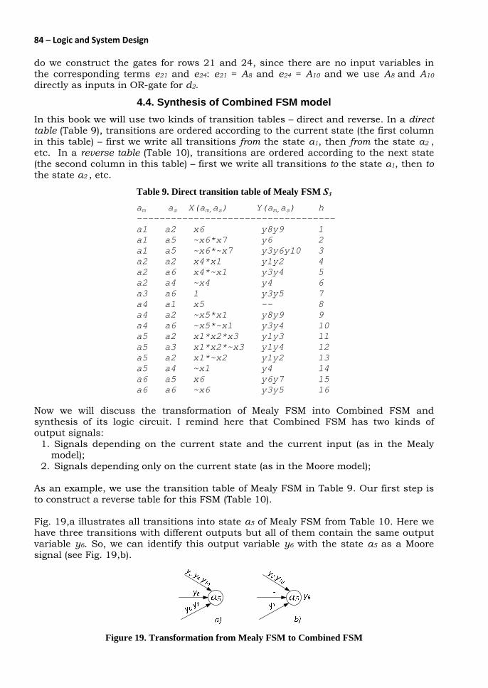
2. Signals depending only on the current state (as in the Moore model); As an example, we use the transition table of Mealy FSM in Table 9. Our first step is to construct a reverse table for this FSM (Table 10). Fig. 19,a illustrates all transitions into state a5 of Mealy FSM from Table 10. Here we have three transitions with different outputs but all of them contain the same output variable y6. So, we can identify this output variable y6 with the state a5 as a Moore signal (see Fig. 19,b).
Figure 19. Transformation from Mealy FSM to Combined FSM
Chapter 4 Algorithmic state machines and finite state machines – 85
Table 10. Reverse transition table of Mealy FSM S3
am as X(am,as) Y(am,as) H --------------------------------- a4 a1 x5 -- 1 a2 a2 x4*x1 y1y2 2 a1 a2 x6 y8y9 3 a4 a2 ~x5*x1 y8y9 4 a5 a2 x1*x2*x3 y1y3 5 a5 a2 x1*~x2 y1y2 6 a5 a3 x1*x2*~x3 y1y4 7 a2 a4 ~x4 y4 8 a5 a4 ~x1 y4 9 a1 a5 ~x6*x7 y6 10 a1 a5 ~x6*~x7 y3y6y10 11 a6 a5 x6 y6y7 12 a4 a6 ~x5*~x1 y3y4 13 a2 a6 x4*~x1 y3y4 14 a3 a6 1 y3y5 15 a6 a6 ~x6 y3y5 16
After this, the transformation of Mealy FSM into Combined model is trivial. Let us return to the reverse Table 10 and begin to construct the reverse transition table of Combined FSM S4 (Table 11 In Table10, we look at the transitions to each state, beginning from transitions to state a1. Let Ys be the set of output variables at the transitions into state as (Y5 = {y3, y6, y7, y10} in Fig19,a or in Table 10) and YsMoore be the subset of common output variables at all transitions into as (Y5Moore = {y6} in Fig19,a or in Table 10). Then, in Table 11, we delete YsMoore from the column Y(am,as) at each row with transition to as and write YsMoore next to as in the column Y(as). In our example:
Y1Moore = Y2Moore = Ø; Y3Moore = { y1, y4}; Y4Moore = { y4}; Y5Moore = { y6}; Y6Moore = { y3}.
Table 11. Reverse transition table of Combined FSM S4
am as Y(as) X(am,as) Y(am,as) H --------------------------------- a4 a1 -- x5 -- 1 a1 a2 -- x6 y8y9 2 a2 a2 -- x4*x1 y1y2 3 a4 a2 -- ~x5*x1 y8y9 4 a5 a2 -- x1*x2*x3 y1y3 5 a5 a2 -- x1*~x2 y1y2 6 a5 a3 y1y4 x1*x2*~x3 -- 7 a2 a4 y4 ~x4 -- 8 a5 a4 y4 ~x1 -- 9 a1 a5 y6 ~x6*~x7 y3y10 10 a1 a5 y6 ~x6*x7 -- 11 a6 a5 y6 x6 y7 12 a2 a6 y3 x4*~x1 y4 13 a3 a6 y3 1 y5 14 a4 a6 y3 ~x5*~x1 y4 15 a6 a6 y3 ~x6 y5 16
86 – Logic and System Design
Now we consider the design of the logic circuit of Combined FSM. For this, let us return to the Mealy FSM S1 with direct transition Table 1. Its reverse transition table is presented in Table 12. Immediately from this table we construct the direct transition table of Combined FSM S1 (Table 13). To construct the logic circuit for this FSM we should encode the states and construct FSM structure table. But before state assignment we will make one more step.
Table 12. Reverse transition table of Mealy FSM S1
Unlike the transition table of the Mealy FSM, Table 13 contains many empty entries in the column Y(am,as). It means that all output variables are equal to zero in these rows. If, after state assignment, we get an empty entry in column D(am,as) for such a row, we shouldn’t construct a product for this row, because all output variables and input memory functions are equal to zero in this row. Now we will try to maximize the number of such rows in the structure table of S5.
Table 13. Direct transition table of Combined FSM S5
Table 13 contains one row with empty entry in the column Y(am,as) for the next states a1 (row 14) and a3 (row 2), two rows for a4 (rows 4 and 7), one row for a5 (row 9) and
am as X(am,as) Y(am,as) H a5
a5
a6
a1
~x6x7
~x6~x7
x6
y3y6y10
- y6y7
1 2 3
a1
a1
a2
a4
a5
a2
x1x2x3
x1~x2
x4x1
~x5x1
x6
y1y3
y1y2
y8y9
y8y9
y8y9
4 5 6 7 8
a1 a3 x1x2~x3 y6y7 9 a1
a2 a4 ~x1
~x4 y4
y4 10 11
a4 a5 x5 y5y6y7 12 a2
a3
a4
a6
a6
x4~x1
1 ~x5~x1
~x6
y3y4
y3y4
y3y4
y3y4
13 14 15 16
am Y( am) as X(am,as) Y(am,as) H a1 --
-- -- --
a2
a3
a2
a4
x1x2x3
x1x2~x3
x1~x2
~x1
y1y3
- y1y2
-
1 2 3 4
a2 -- -- --
a2
a6
a4
x4x1
x4~x1
~x4
y8y9
- -
5 6 7
a3 y6y7 a6 1 - 8 a4 y4 a5
a2
a6
x5
~x5x1
~x5~x1
- y8y9
--
9 10 11
a5 y5y6y7
a2
a1
a1
x6
~x6x7
~x6~x7
y8y9
y3y6y10
-
12 13 14
a6 y3y4 a1
a6 x6
~x6 y6y7
- 15 16
Chapter 4 Algorithmic state machines and finite state machines – 87
four rows for a6 (rows 6, 8, 11 and 16). This information is presented in the first two columns of Table 14, z(as) is the number of empty entries in column Y(am,as) for the next state as in Table 13. So, if we use zero code for states a1 or a3 or a5, we shouldn’t construct a product for one row (z(a1) = z(a3) = z(a5) = 1), if we use zero code for state a4 – for two rows (z(a4) = 2); but if we use zero code for state a6, we will construct four product less (z(a6) = 4). Thus, we use code 000 for state a6 with max z(as). State assignment for other states is presented in Table 15. We have used here the same algorithm as we have used previously for Mealy and Moore models.
Table 16. Structure table of Combined FSM S5
am Y(am) K(am) as K(as) X(am,as) Y(am,as) D(am,as) H a1 --
-- -- --
010 a2
a3
a2
a4
001 101 001 100
x1x2x3
x1x2~x3
x1~x2
~x1
y1y3
- y1y2
-
d3
d1d3
d3
d1
1 2 3 4
a2 -- -- --
001 a2
a6
a4
001 000 100
x4x1
x4~x1
~x4
y8y9
- -
d3
- d1
5 6 7
a3 y6y7 101 a6 000 1 - - 8 a4 y4 100 a5
a2
a6
110 001 000
x5
~x5x1
~x5~x1
- y8y9
-
d1d2 d3
-
9 10 11
a5 y5y6y7
110 a2
a1
a1
001 010 010
x6
~x6x7
~x6~x7
y8y9
y3y6y10
-
d3
d2
d2
12 13 14
a6 y3y4 000 a1
a6 010 000
x6
~x6 y6y7
- d2
- 15 16
Table 16 is the structure table of Combined FSM S5. We have three kinds of output variables here:
1. Only Mealy signals: y1, y2, y8, y9, y10. They are written in column Y(am,as) and are not written in column Y(am) in Table 16;
2. Only Moore signals: y4, y5. They are written in the column Y(am) and are not written in column Y(am,as) in Table 16;
3. Combined signals: (both Mealy and Moore type) y3, y6, y7. They are written in both columns Y(am,as) and Y(am) in Table 16.
The logic circuit of FSM S5 is constructed in Fig. 20. In this circuit, Am is a product of state variables for the state am (m = 1, …, 6). The left part of this circuit, exactly as in the synthesis of the Mealy FSM logic circuit, implements input memory functions d1, d2, d3 and Mealy signals y1, y2, y8, y9, y10. As above, we construct one AND-gate for one row of the structure table, but we need not construct the gates for rows 6, 8, 11,
Table 14. Next states with zero outputs
as z(as) t1 t2 t3
a1 1 a3 1 a4 2 a5 1 a6 4 0 0 0
Table 15. State assignment
as p(as) t1 t2 t3
a1 3 0 1 0 a2 5 0 0 1 a3 1 1 0 1 a4 2 10 0 a5 1 1 1 0 a6 4 0 0 0

88 – Logic and System Design
16 because all output variables and input memory functions are equal to zero in these rows in the columns Y(am,as) and D(am,as) in Table 16. As in the Mealy case, we do not construct OR gates for y2 and y10 since they appear only once in the column Y(am,as). Moore signals y4, y5 are constructed as in the synthesis of Moore FSM logic circuit. Signal y4 appears twice near the states a4 and a6 in the column Y(am), so y4 = A4 + A6
and we construct OR gate for this signal. Output signal y5 appears only once in the column Y(am) for the state a5, so we get it straight from A5: y5 = A5.
Combined signal y6 is written in rows 13 and 15 in the column Y(am,as) and near the states a3 and a5 in the column Y(am), so
y6 = e13 + e15 + A3 + A5.
Exactly in the same way
y3 = e1 + e13 + A6; y7 = e15 + A3 + A5.
Figure 20. Logic circuit of Combined FSM S5
4.5. FSM decomposition
In this section, we will discuss a very simple model for FSM decomposition. As an example, we use Mealy FSM S6 (Table 17) and a partition π on the set of its states:
π = {A1, A2, A3}; A1 = {a2, a3, a9}; A2 = {a4, a7, a8}; A3 = {a1, a5, a6}.

Chapter 4 Algorithmic state machines and finite state machines – 89
The number of component FSMs in the FSM network is equal to the number of blocks in partition π. Thus, in our example, we have three component FSMs S1, S2, S3. Let Bm is the set of states in the component FSM Sm. Bm contains the corresponding block of the partition π plus one additional state bm. So, in our example:
S1 has the set of states B1 = {a2, a3, a9, b1}; S2 has the set of states B2 = { a4, a7, a8, b2}; S3 has the set of states B3 = { a1, a5, a6, b3}.
Table 17. Mealy FSM S6
am as X(am,as) Y(am,as) H ------------------------------------------------------- a1 a3 x1*x2*x3 y1y2 1 a1 a6 x1*x2*~x3 y2y12 2 a1 a1 x1*~x2 y1y2 3 a1 a5 ~x1 y1y2y12 4 a2 a2 x6 -- 5 a2 a3 ~x6 y3y5 6 a3 a3 x10 y3y5 7 a3 a9 ~x10*x4 y10y15 8 a3 a8 ~x10*~x4 y5y8y9 9 a4 a6 x7 y13 10 a4 a4 ~x7*x9 y13y18 11 a4 a8 ~x7*~x9 y13y14 12 a5 a6 x1 y16y17 13 a5 a5 ~x1 y7y11 14 a6 a1 x5 y1y2 15 a6 a1 ~x5 y16y17 16 a7 a2 x8 y14y18 17 a7 a4 ~x8 y13y18 18 a8 a7 x9 y4y6 19 a8 a4 ~x9 y6 20 a9 a9 x11*x6 y10y15 21 a9 a2 x11*~x6 y5y8y9 22 a9 a3 ~x11 y3y8y9 23
To construct a transition table for each component FSM we should define the transitions between the states of these FSMs. For this, each transition between two states ai and aj of Mealy FSM S6 from Table 17 should be implemented one after another as one or two transitions in component FSMs. There are two possible cases:
1. In Mealy FSM S6, there is a transition between ai and aj (Fig. 21, left) and both of these states are in the same component FSM Sm. In such a case, we will have the same transition in this component FSM Sm (Fig. 21, right). It means that we must rewrite the corresponding row from the table of FSM S6 into the table of component FSM Sm.
Figure 21. Two states ai and aj are in the same component FSM
90 – Logic and System Design
2. Two states ai and aj are in different component FSMs (Fig. 22). Let ai be in the component FSM Sm (ai ∈ Bm) and aj be in the component FSM Sp (aj ∈ Bp). In such a case, one transition of FSM S6 should be presented as two transitions – one in the component FSM Sm and one in the component FSM Sp:
• FSM Sm transits from ai into its additional state bm with the same input Xh. At its output, we have the same output variables from set Yt plus one additional output variable zj, where index j is the index of state aj
in the component FSM Sp. • FSM Sp is in its additional state bp. It transits from this state into state
aj with input signal zj, that is an additional output variable in the component FSM Sm. The output at this transition is Y0 – the signal with all output variables being equal to zero.
Figure 22. Two states ai and aj are in the different component FSMs
Thus, the procedure for FSM decomposition is reduced to: a) Copying the row
ai aj X(ai ,aj) Y(ai ,aj)
from the table of the decomposed FSM S to the table of the component FSM Sm if both states ai and aj are the states of Sm;
b) Replacing the row
ai aj X(ai ,aj) Y(ai ,aj) in the table of the decomposed FSM S by the row
ai bm X(ai ,aj) Y(ai ,aj) zj
in the table of the component FSM Sm, and by the row
bp aj zj -- in the table of the component FSM Sp, if ai is the state of Sm and aj is the state of Sp.
As a result of decomposition of FSM S6, we obtain the network with three component FSMs in Fig. 23. Their transition tables are presented in Tables 18 – 20. Now we will illustrate some examples of transitions for cases (a) and (b):
• In FSM S6, there is a transition from state a2 to state a3 with input ~x6 and
output y3y5 (row 6 in Table 17). As both these states a2 and a3 are in the same component FSM S1, in this FSM there is a transition from a2 to a3 with the same input ~x6 and the same output y3y5 (row 2 in Table 18). Exactly in the same way, we rewrite row 12 of Table 17 into row 3 of Table 19 and row 2
Chapter 4 Algorithmic state machines and finite state machines – 91
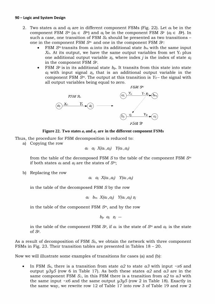
of Table 17 into row 2 of Table 20 because the current states and the next states are in the same component FSMs.
• In FSM S6, there is a transition from state a3 to state a8 with input ~x10*~x4 and the output y5y8y9 (row 9 in Table 17). Since a3 is the state of component FSM S1 and a8 is the state of another component FSM S2, in FSM S1 there is a transition from a3 to b1 with the same input ~x10*~x4 and output y5y8y9z8 (row 5 in Table 18). The last output z8 is the input of FSM S2 that wakes this FSM up and transits it from state b2 to state a8 (row 8 in Table 19). Similarly, we convert row 1 of Table 17 into two rows – the first in Table 20 and the tenth in Table 18 etc. Note that we add the last row in each FSM table to remain component FSMs in the state bm when each zj is equal to zero.
Figure 23. Network with three component FSMs
Table 18. Component FSM S1
am as X(am,as) Y(am,as) H --------------------------------------------------------------------- a2 a2 x6 -- 1 a2 a3 ~x6 y3y5 2 a3 a3 x10 y3y5 3 a3 a9 ~x10*x4 y10y15 4 a3 b1 ~x10*~x4 y5y8y9z8 5 a9 a9 x11*x6 y10y15 6 a9 a2 x11*~x6 y5y8y9 7 a9 a3 ~x11 y3y8y9 8 b1 a2 z2 -- 9 b1 a3 z3 -- 10 b1 b1 ~z2*~z3 -- 11
Table 19. Component FSM S2
am as X(am,as) Y(am,as) H --------------------------------------------------------------------- a4 b2 x7 y13z6 1 a4 a4 ~x7*x9 y13y18 2 a4 a8 ~x7*~x9 y13y14 3 a7 b2 x8 y14y18z2 4 a7 a4 ~x8 y13y18 5 a8 a7 x9 y4y6 6 a8 a4 ~x9 y6 7 b2 a8 z8 -- 8 b2 b2 ~z8 -- 9

92 – Logic and System Design
Let us discuss how this network works. Let a1 be an initial state in FSM S6. After decomposition, state a1 is in FSM S3, so, at the beginning, just FSM S3 is in state a1. Other FSMs are in states b1 and b2 correspondingly. It is possible to say that they “are sleeping” in these states. FSM S3 transits from the state to the state until x1*x2*x3 = 1 in state a1 (see row 1 in Table 20). Only at this transition FSM S3 produces output signal z3 and transits into state b3 (sleeping state). This signal z3 is the input signal of FSM S1. It wakes FSM S1 up and transits it from the sleeping state b1 to state a3 (see row 10 in Table 18). Now FSM S1 transits from the state to the state until, in state a3, it transits into state b1 with input signal ~x10*~x4 = 1 and wakes FSM S2 up by signal z8 (see row 5 in Table 18 and row 8 in Table 19).
Table 20. Component FSM S3
am as X(am,as) Y(am,as) H --------------------------------------------------------------------- a1 b3 x1*x2*x3 y1y2z3 1 a1 a6 x1*x2*~x3 y2y12 2 a1 a1 x1*~x2 y1y2 3 a1 a5 ~x1 y1y2y12 4 a5 a6 x1 y16y17 5 a5 a5 ~x1 y7y11 6 a6 a1 x5 y1y2 7 a6 a1 ~x5 y16y17 8 b3 a6 z6 -- 9 b3 b3 ~z6 -- 10
Unlike FSMs S1 and S3, the component FSM S2 has two possibilities to wake other component FSMs up – in state a4 with input signal x7 = 1 (row 1 of Table 19) and in state a7 with input signal x8 = 1 (row 4 in the same Table), etc. Thus, each time all component FSMs, except one, are in the states of type bm and only one of them is in the state of type ai.

Chapter 5 Multilevel and Multioutput Synthesis
In this Chapter, we will concentrate on the multilevel minimization of logic circuits. Several simple and straightforward methods for obtaining circuit structure with more than two levels will be considered. In these methods, we will present four procedures – factoring, term decomposition, full inclusion and equal gates removal. At the end of the Chapter we will show how to construct optimized multilevel and multioutput circuits of Finite State Machines using only these four procedures.
5.1 Factoring 5.1.1 Two factoring structures. The first example of factoring is presented in Fig. 1. The left part of this figure implements the function
f1 = x1x2x'3x4 + x1x2x'5 + x1x2x3x'4. (1)
Figure 1. Factoring from all terms
All AND-gates of this circuit have the common input x1x2, so we can factor this common term (we call it a factor) in function (1):
f1 = x1x2 (x'3x4 + x'5 + x3x'4) (2)
The corresponding logic circuit is constructed in Fig. 1,b. In this circuit, e"1, e"2 and e"3 contain inputs remained after deleting factor x1x2 from e1, e2 and e3, and if there remains only one letter (x'5 in our example), it will be an exact input into OR-gate. Let us suppose again that the cost of a gate is equal to the number of its inputs, and that the cost of logic circuit is the sum of the costs of gates – the total number of inputs into all gates. If C1 and C2 are the costs of circuits before and after factoring then C1 – C2 is a minimization or a gain of factoring. We can evaluate the gain of factoring for the common term z by the formula
w(z) = m(n - 1) - 1 + r. (3) Here m is the number of letters in factor z, n is the number of gates in factoring and r is the number of gates in which only one letter is left after factoring. In our example w(z) = 2(3 - 1) - 1 + 1 = 4. Really, if we count C1 and C2 in Fig.1, C1 – C2 = 4. One more example of factoring is presented in Fig. 2. Unlike the previous example, here we can factor the common term x1x3x'4 only from two AND-gates, not from all of them:

94 – Logic and System Design
f2 = x1x2x3x'4x5 + x4x6x'7 + x1x'2x3x'4x'5 + x'1x'2; f2 = x1x3x'4 (x2x5 + x'2x'5) + x4x6x'7 + x'1x'2.
The result of factoring is shown in Fig. 2,b. On the right, we have OR-gate with three inputs – two of them from all AND-gates that do not take part in factoring (e2, e4) and the third one – from the output of the factoring structure for e1, e3 similar to Fig. 1,b.
Figure 2. Factoring not from all terms
Again, we can evaluate the gain of factoring for the common term z by the formula
w(z) = m(n - 1) - 2 + r. (4)
Here m, n, and r are the same as in expression (3). See if you can understand why “-2” is used in this formula instead of “-1”. We discussed here two structures for factoring – structure one in Fig. 1,b (factoring from all AND-gates) and structure two in Fig. 2,b (factoring from some of AND-gates). The duality of Boolean functions permits us to use factoring not only for the sum-of-products, but for the product-of-sum as well (see Fig.3 and Fig. 4).
Figure 3. The first factoring structure for the product-of-sums
5.1.2 More than one factor. In the previous examples we have only one possible factor for factoring. Now we will discuss a case with several probable factors. As an
Chapter 5 Multilevel and Multioutput Synthesis – 95
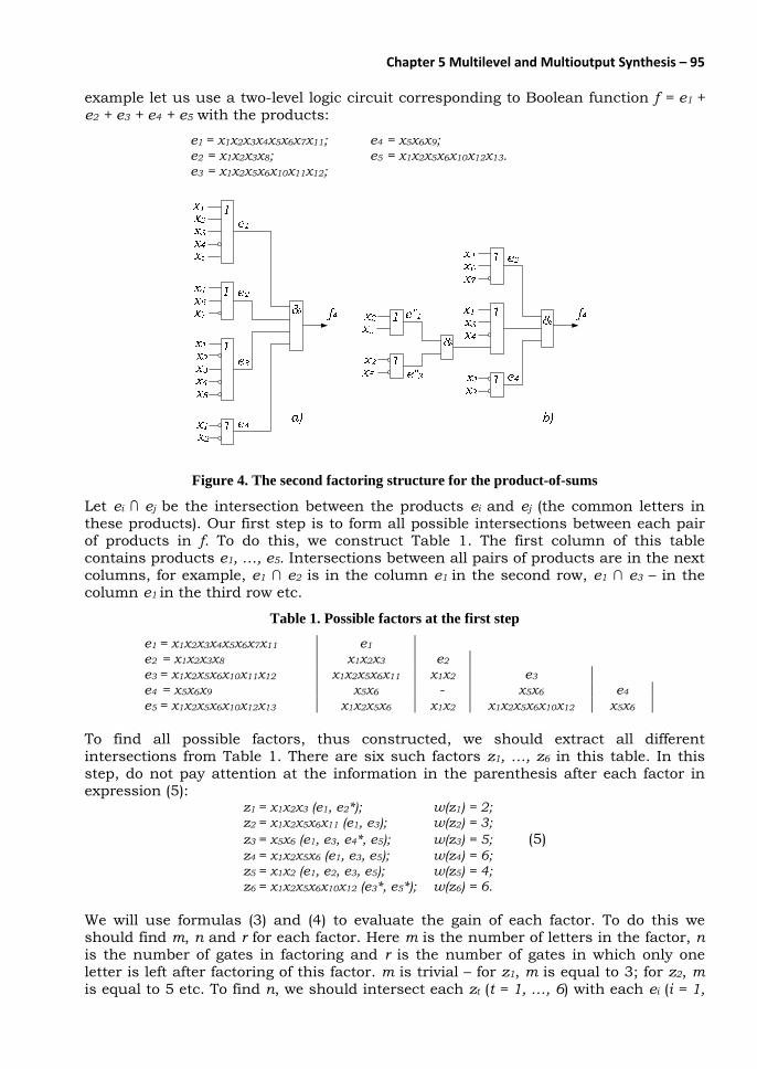
example let us use a two-level logic circuit corresponding to Boolean function f = e1 + e2 + e3 + e4 + e5 with the products:
e1 = x1x2x3x4x5x6x7x11; e4 = x5x6x9; e2 = x1x2x3x8; e5 = x1x2x5x6x10x12x13. e3 = x1x2x5x6x10x11x12;
Figure 4. The second factoring structure for the product-of-sums
Let ei ∩ ej be the intersection between the products ei and ej (the common letters in these products). Our first step is to form all possible intersections between each pair of products in f. To do this, we construct Table 1. The first column of this table contains products e1, …, e5. Intersections between all pairs of products are in the next columns, for example, e1 ∩ e2 is in the column e1 in the second row, e1 ∩ e3 – in the column e1 in the third row etc.
Table 1. Possible factors at the first step
e1 = x1x2x3x4x5x6x7x11 e1
e2 = x1x2x3x8 x1x2x3 e2 e3 = x1x2x5x6x10x11x12 x1x2x5x6x11 x1x2 e3 e4 = x5x6x9 x5x6 - x5x6 e4 e5 = x1x2x5x6x10x12x13 x1x2x5x6 x1x2 x1x2x5x6x10x12 x5x6
To find all possible factors, thus constructed, we should extract all different intersections from Table 1. There are six such factors z1, …, z6 in this table. In this step, do not pay attention at the information in the parenthesis after each factor in expression (5):
z1 = x1x2x3 (e1, e2*); w(z1) = 2; z2 = x1x2x5x6x11 (e1, e3); w(z2) = 3; z3 = x5x6 (e1, e3, e4*, e5); w(z3) = 5; (5) z4 = x1x2x5x6 (e1, e3, e5); w(z4) = 6; z5 = x1x2 (e1, e2, e3, e5); w(z5) = 4; z6 = x1x2x5x6x10x12 (e3*, e5*); w(z6) = 6.
We will use formulas (3) and (4) to evaluate the gain of each factor. To do this we should find m, n and r for each factor. Here m is the number of letters in the factor, n is the number of gates in factoring and r is the number of gates in which only one letter is left after factoring of this factor. m is trivial – for z1, m is equal to 3; for z2, m is equal to 5 etc. To find n, we should intersect each zt (t = 1, …, 6) with each ei (i = 1,

96 – Logic and System Design
…, 5). If zt is contained in ei, then zt is the factor of ei and we write ei in the parenthesis after zt. Thus, for z1, z2 and z6, n is equal to 2, for z3 and z5, n is equal to 4 etc. While performing such intersections, it is possible to find r as well. For example, when we intersect z1 with e2 we see that z1 є e2 and only one letter is left after factoring z1 from e2, because z1 has three letters but e2 has four. The symbol * next to e2 in the line for z1 means that only one letter is left. We have the same for z3 (e4*) and z6 (e3*, e5*). When we have m, n and r for each factor, the evaluation is trivial. w(zt) for each zt is presented in the second column of (5). In the first step of factoring, we use a factor with a maximal gain. If we have several such factors (two in our example – z4 and z6) it is possible to implement one of the following strategies:
1. Take the first of such factors (the simplest strategy); 2. Take the factor with maximal length from these factors; 3. Take the factor contained in the maximum number of gates; 4. Move one step forward for each such factor and select factor after the
second evaluation step etc. We will use the first trivial strategy and select z4 with
w(z4) = 6 = max.
Figure 5. The circuit after the first step of factoring
The circuit after factoring of z4 is shown in Fig. 5. It implements two functions presented as sum-of-product:
1. Function f is the sum-of-products with three AND-gates, one of them contains the factor z4, and two others – the products that do not take part in factoring;
2. Function t1 is the sum-of-products with three AND-gates, each of them corresponds to one of the products that took part in factoring. These ANDs have inputs remaining after factoring of z4.
Fig. 6 presents the factoring process. The first box in this figure contains the set of products e1, …, e5, the second one – the partitioning of this set into two subsets after the first step. Thus, we must continue the factoring separately for two functions presented as sum-of-products – function f containing products e2, e4, e6 and function t1 containing products e''1, e''3, e''5. A similar partition will be at each next step so the process of factoring converges very fast.
Chapter 5 Multilevel and Multioutput Synthesis – 97
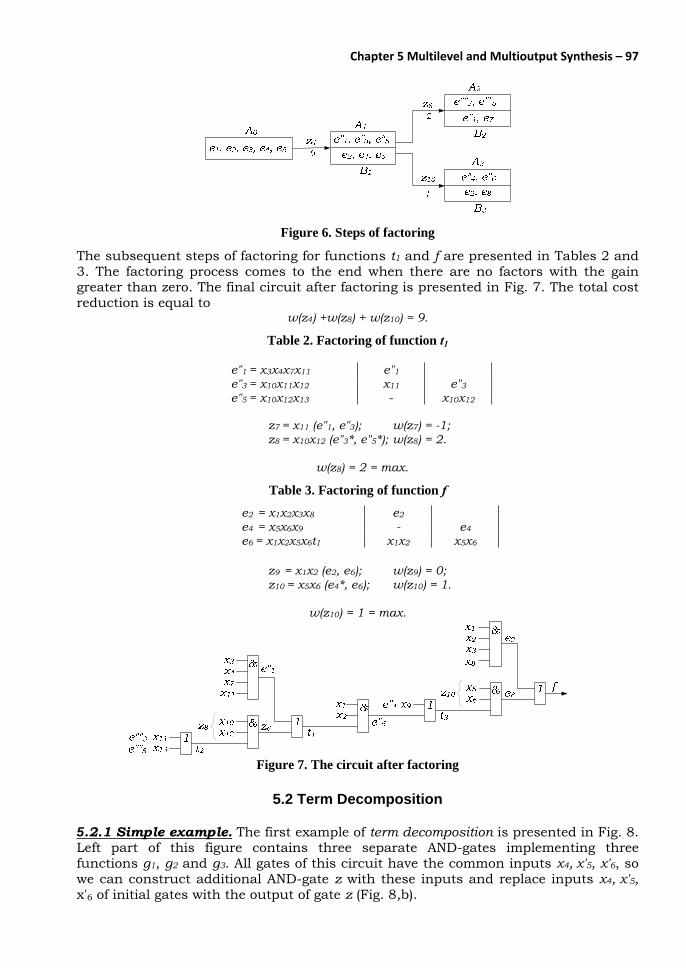
Figure 6. Steps of factoring
The subsequent steps of factoring for functions t1 and f are presented in Tables 2 and 3. The factoring process comes to the end when there are no factors with the gain greater than zero. The final circuit after factoring is presented in Fig. 7. The total cost reduction is equal to
w(z4) +w(z8) + w(z10) = 9.
Table 2. Factoring of function t1
z7 = x11 (e"1, e"3); w(z7) = -1; z8 = x10x12 (e"3*, e"5*); w(z8) = 2.
w(z8) = 2 = max.
Table 3. Factoring of function f
e2 = x1x2x3x8 e2 e4 = x5x6x9 - e4 e6 = x1x2x5x6t1 x1x2 x5x6
z9 = x1x2 (e2, e6); w(z9) = 0; z10 = x5x6 (e4*, e6); w(z10) = 1.
w(z10) = 1 = max.
Figure 7. The circuit after factoring
5.2 Term Decomposition
5.2.1 Simple example. The first example of term decomposition is presented in Fig. 8. Left part of this figure contains three separate AND-gates implementing three functions g1, g2 and g3. All gates of this circuit have the common inputs x4, x'5, x'6, so we can construct additional AND-gate z with these inputs and replace inputs x4, x'5, x'6 of initial gates with the output of gate z (Fig. 8,b).
e"1 = x3x4x7x11 e"1 e"3 = x10x11x12 x11 e"3 e"5 = x10x12x13 - x10x12

98 – Logic and System Design
Figure 8. Simple term decomposition
If C1 and C2 are the costs of circuits before and after term decomposition then C1 – C2
is a minimization or a gain of term decomposition. We can evaluate the gain of term decomposition for the common term z by the formula
w(z) = m(n - 1) - n + r. (6) Here m is the number of letters in the common term z, n is the number of gates in term decomposition and r is the number of functions (initial AND-gates) equal to the common term. In our example w(z) = 3(3 - 1) - 3 + 1 = 4. Really, if we count C1 and C2
in Fig. 8, C1 – C2 = 4. 5.2.2 More than one common term. In the previous example, we had only one possible term for term decomposition. Now we will discuss the case with several probable common terms. As an example let us use a circuit in Fig. 9 that corresponds to the following products:
Figure 9. Logic circuit before term decomposition
As in factoring, the algorithm of term decomposition consists of several steps. The first step is to form intersections between each pair of products to find all possible common terms containing two or more variables (see Table 4). We will use formula (6) to evaluate the gain of each common term. To do this we should find m, n and r for each term: m is trivial – it is the number of letters in the common term. For z1, m is
g1 = x1x2x3x4x5x6x7x11; g2 = x1x2x3x8; g3 = x1x2x5x6x10x11x12;
g4 = x5x6x9; g5 = x1x2x5x6x10x12.

Chapter 5 Multilevel and Multioutput Synthesis – 99
equal to 3; for z2, m is equal to 5 etc. It is clear that the common term with one variable makes no sense in term decomposition.
Table 4. Possible common terms at the first step
g1 = x1x2x3x4x5x6x7x11 g1
g2 = x1x2x3x8 x1x2x3 g2 g3 = x1x2x5x6x10x11x12 x1x2x5x6x11 x1x2 g3 g4 = x5x6x9 x5x6 - x5x6 g4 g5 = x1x2x5x6x10x12 x1x2x5x6 x1x2 x1x2x5x6x10x12 x5x6
z1 = x1x2x3 (g1, g2); w(z1) = 1; z2 = x1x2x5x6x11 (g1, g3); w(z2) = 3; z3 = x5x6 (g1 g2, g4, g5); w(z3) = 2; (7) z4 = x1x2x5x6 (g1, g3, g5); w(z4) = 5; z5 = x1x2 (g1,g2, g3, g5); w(z5) = 2; z6 = x1x2x5x6x10x12 (g3, g5*); w(z6) = 5.
To find n, we should intersect each zt (t = 1, …, 6) with each gi (i = 1, …, 5). If zt є gi, then zt is the common term for gi and we write gi in the parenthesis after zt. While performing such an intersection it is possible to find r as well. For example, when we intersect z6 with g5 we see that z6 = g5. The symbol * near g5 in the line for z6 means that the product g5 is equal to the common term z6. When we have m, n and r for each common term, the evaluation is trivial – w(zt) for each zt is presented in the second column of (7). In the first step of term decomposition, we use a common term with the maximal gain. If we have several such terms (two in our example – z4 and z6), as in factoring, it is possible to implement the following several strategies:
1. Take the first of such common terms (the simplest strategy); 2. Take the common term with maximal length from these common terms; 3. Take the common term contained in the maximum number of gates; 4. Move one step forward for each such common term and select common term
after the second step evaluation etc. We will use the first strategy and select z4 with
w(z4) = 5 = max.
The circuit after decomposition of z4 is shown in Fig. 10.
Figure 10. Logic circuit after the first step of term decomposition

100 – Logic and System Design
Unlike factoring, where we had a partition of products into two subsets after each step, there is no partition of initial products is here. Moreover, the common term taking part in term decomposition should be added to the set of products and will be used at the next step together with other products. Only the product equal to the common term should be excluded from the list of products in the next step of term decomposition. The next step of term decomposition is presented in Table 5. The process comes to the end when there are no factors with the gain greater than zero. The final circuit after term decomposition is shown in Fig. 11, the whole process is illustrated by Fig. 12.
Table 5. The second (final) step of term decomposition
g"1 = x3x4x7x11z4 g"1
g2 = x1x2x3x8 - g2 g"3 = x10x11x12z4 x11z4 - g"3 g4 = x5x6x9 - - - g4 g"5 = x10x12z4 - - x10x12z4 - g"5 z4 = x1x2x5x6 x1x2 - x5x6 - z7 = x11z4 (g"1, g"3); w(z1) = 0; z8 = x1x2 (g2, z4); w(z2) = 0; z9 = x10x12z4 (g"3, g"5*); w(z9) = 2; z10 = x5x6 (g4, z4); w(z10) = 0.
w(z9) = 2 = max. The total cost reduction is equal to
w(z4) + w(z9) = 7.
Figure 11. The circuit after t-decomposition
Figure 12. Steps of t-decomposition
5.2.3 Term decomposition for OR gates. Term decomposition can be applied to OR gates as well. We will give the next example without any comments and you can fulfill each step on your own (Fig. 13).

Chapter 5 Multilevel and Multioutput Synthesis – 101
Figure 13. Term decomposition for OR gates
5.3 Gate inclusion
Let us define gate m as included in gate n, or gate n as covering gate m, if they have the same type (both AND or both OR) and the set of inputs of gate m is a subset of the set of inputs of gate n. The simplest case of gate inclusion is presented in Fig 14,a. In this case, we can replace inputs of gate n, equal to the inputs of gate m (x1 and x2 in our example), with the output of gate m (Fig. 14,b).
Figure 14. Gate inclusion
5.4 Removal of equal gates
Let us define as gates m and n equal, if they have the same type (both AND or both OR) and the set of inputs of gate m is equal to the set of inputs of gate n. The circuit in Fig. 15,a contains four equal two-input AND-gates. In this case, we should
1. Remove all equal gates, except one (gates l, m and n in our example); 2. Connect inputs of gates (t, p and q) formerly connected to the outputs of
removed gates, with the output of the remained gate (gate k in our example).

102 – Logic and System Design
The last two procedures – gate inclusion and removal equal gates are covered by term decomposition. Really, in the first step of term decomposition – pair intersection, we can find equal gates and gates included into other gates. However, term decomposition has two problems: (1) the large number of gates taking part in this procedure; (2) multiple comparisons demand a lot of intersections between sets of inputs. It is more simple and faster to check gate inclusion and remove equal gates before term decomposition. Moreover, after these two procedures, only gates with three and more inputs remain for term decomposition (see if you can understand why it is so).
Figure 15. Removal three equal AND-gates
5.5 Multilevel and multioutput circuits for Finite State Machines
In Section 4.2.6 of Chapter 4, we considered a very simple method for synthesis of the two level FSM logic circuit from its structure table. Recall that we have used the term
eh = Am Xh
in accordance with the h row of such a table (h = 1, …, H). Here Am is a product of state variables corresponding to the current state am written in the h row, Xh is a product of input variables written in the same row, and H is the number of rows in the structure table. Then we constructed H AND-gates corresponding to terms e1, …, eH. If the output variable yn appears only once, for example, in row i of the structure table, we obtain the output yn at the output of AND-gate number i. If the output variable yn is written in several rows, for example, in rows p1, …, pT of the structure table, we construct OR-gate with T inputs and connect these inputs with the outputs of AND-gates p1, …, pT. The output yn is obtained at the output of this OR-gate. In exactly the same way, we construct OR-gate for each input memory function which occurs more than once in the column D(am,as) of the structure table. The logic circuit of FSM thus constructed contains not more than H AND-gates and not more than (N + R) OR-gates where N and R are the numbers of output variables and input memory functions in the FSM structure table.
In this section, we will use the reverse structure table. Recall that in such a table all transitions are ordered according the next state – first we write all transitions to state a1, then to state a2 , etc. As an example we will consider the logic synthesis of FSM S,
Chapter 5 Multilevel and Multioutput Synthesis – 103
Table 6 is its reverse structure table. As in four previous sections, we assume that the circuit cost is equal to the sum of inputs of its gates.
Table 6. The reverse structure table of FSM S a1 001 a1 001 x8*x7 y7y9y14y15 d3 1 a1 001 a1 001 x8*~x7*x1*x9*x5 y13 d3 2 a1 001 a1 001 ~x8*x1*x9*x5 y13 d3 3 a3 011 a1 001 x9*x5 y13 d3 4 a4 000 a1 001 x4*~x9*x3 y2y10y12 d3 5 a5 010 a1 001 x4 -- d3 6 a1 001 a2 100 x8*~x7*~x1 y1y2y3 d1 7 a1 001 a2 100 ~x8*~x1 y1y2y3 d1 8 a2 100 a2 100 ~x2 -- d1 9 a2 100 a3 011 x2 y4 d2d3 10 a4 000 a3 011 x4*~x9*~x3 y5y6 d2d3 11 a4 000 a3 011 x4*x9 y5y6 d2d3 12 a1 001 a4 000 x8*~x7*x1*~x9*x3*~x6 y7y8y9 -- 13 a1 001 a4 000 ~x8*x1*x9*~x5 y7y8y9 -- 14 a3 011 a4 000 x9*~x5 y7y8y9 -- 15 a3 011 a4 000 ~x9*x3*~x6 y7y8y9 -- 16 a3 011 a4 000 ~x9*~x3 y7y8y9 -- 17 a1 001 a4 000 ~x8*x1*~x9*x3*~x6 y7y8y9 -- 18 a1 001 a4 000 ~x8*x1*~x9*~x3 y7y8y9 -- 19 a1 001 a4 000 x8*~x7*x1*~x9*~x3 y7y8y9 -- 20 a4 000 a4 000 ~x4 -- -- 21 a1 001 a4 000 x8*~x7*x1*x9*~x5 y7y8y9 -- 22 a1 001 a5 010 x8*~x7*x1*~x9*x3*x6 y10y11y12 d2 23 a3 011 a5 010 ~x9*x3*x6 y10y11y12 d2 24 a1 001 a5 010 ~x8*x1*~x9*x3*x6 y10y11y12 d2 25 a5 010 a5 010 ~x4 -- d2 26 The structure table is divided into M arrays, each of which corresponds to the set of transitions into one state. For FSM in Table 6, M is equal to five. In several initial steps, we will separately design logic circuits for transitions into each state. Moreover, even then we will construct circuits separately for each subset of output signals. A design of the logic circuit consists of the following steps: Step 1. Divide each array of transitions to the state as (s = 1, …, M) into as many subarrays, as the number of different microinstructions (the subsets of output variables) in the column Y(am, as) within this array. For example, in Table 6, transitions into state a1 have four microinstructions:
y7, y9, y14, y15; y13; (8) y2, y10, y12; ∅ .
We should include the empty microinstruction, corresponding to row 6, in this list because not all of input memory functions are equal to zero at this transition (d3 = 1) and we must construct AND-gate for this row.
Thus, in our example we have four such subarrays containing
1. Row 1 with outputs y7, y9, y14, y15; 2. Rows 2, 3, 4 with output y13; 3. Row 5 with outputs y2, y10, y12; 4. Row 6 without output signals.
104 – Logic and System Design
Step 2. For each subarray corresponding to one of microinstruction in (8), construct as many AND-gates as the number of rows in this subarray of the structure table. These gates implement products AmX(am,as), corresponding to each row. In our example for the transitions into a1 we have six such AND-gates (see Fig.16,a).
Figure 16. Logic circuit for transitions into state a1
Step 3. If some subarray contains more than one row, connect the outputs of corresponding AND-gates, constructed at step 2 for the subarray, with OR-gate to form the signals of microoperations (output variables) and input memory functions written in the rows of this subarray (rows 2, 3, 4 for y13 – Fig. 16,a). Step 4. Factor the logic circuits constructed in point 3 using the algorithm described in Section 5.1 ‘Factoring’. Let us do this for functions y13, d3. Table 7 contains the first step of this factoring. We made all pair intersections between products corresponding to rows with y13, d3 and found two possible factors z1 and z2. We factor z2 with max gain (see Fig. 16,b). It is possible to make one more simplification in the circuit in Fig. 16,b. OR-gate has input t2 and AND-gates connected with this OR-gate have inputs t′2. According Boolean algebra A + A'B = A + B, so we can delete inputs t′2 from AND-gates. To make such minimization we do not have to write any formulas. If some OR-gate has some

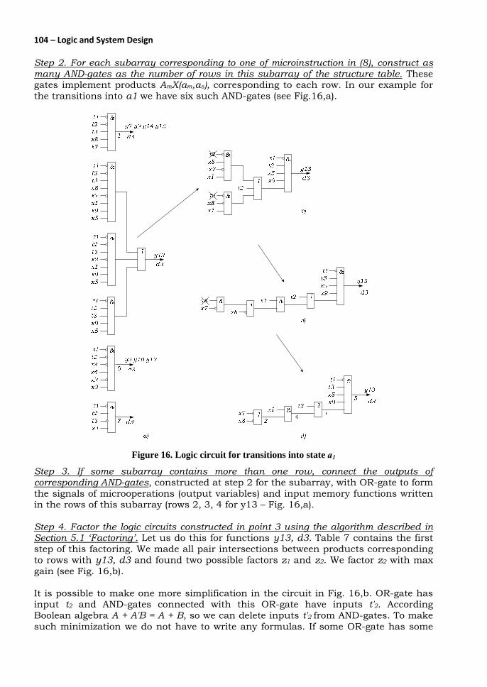
Chapter 5 Multilevel and Multioutput Synthesis – 105
input p (p') we should check all AND-gates connected with this OR-gate and remove inputs p' (p) from these AND-gates.
Table 7. The first step of factoring for y13 and d3
e1 = t'1t'2t3x8x'7x1x9x5 e1
e2 = t'1t'2t3x'8x1x9x5 t'1t'2t3x1x9x5 e2 e3 = t'1t2t3x9x5 t'1t3x9x5 t'1t3x9x5
z1 = t'1t'2t3x1x9x5 (e1, e2*); w(z1) = 6(2 - 1) - 2 + 1 = 5; z2 = t'1t3x9x5 (e1, e2, e3*); w(z2) = 4(3 - 1) - 1 + 1 = 8;
w(z2) = 8 = max.
The last step of factoring is shown in Table 8 and Fig. 16,c. After removing input x8 from AND-gate with two inputs we must remove this AND-gate as well, and transfer input x′7 into the OR-gate. The final step of factoring is presented in Fig. 16,d.
Table 8. The second steps of factoring for y13, d3
e′′1 = x8x′7x1 e′′1 e′′2 = x’8x1 x1
z3 = x1 (e′′1, e′′2*); w(z3) = 1(2 – 1) – 1 + 1 = 1;
w(z3) = 1 = max.
Logic circuit after factoring for transitions into state a1 contains seven gates – we numbered gates after the last step. Each step of circuit factoring for transitions into states a2 and a3 is presented in Fig.17 and Fig. 18. Logic circuits for transitions into states a4 and a5 without intermediate steps are shown in Fig. 19 and Fig. 20. We have left the design of these last circuits to our readers as exercise to be done on their own. At last, we bring all these circuits together in Fig. 21.
Figure 17. Logic circuit for transitions into state a2
Step 5. Delete equal gates in the logic circuit thus constructed. If we look at the circuit after factoring in Fig. 21 we will find that it contains some equal gates. For example, six two-input OR-gates OR2, OR9, OR14, OR16, OR18 and OR27 are equal because they have the same type and the same inputs. However, AND-gates AND3(x1,2) and AND28(x1,27) are not equal because they have inputs from different gates. Тo find that they are also equal we must determine that OR2 and OR27 are equal and change the
106 – Logic and System Design
input 27 by input 2 in the description of AND28. Therefore, to find that two gates are equal in a multilevel circuit we should find that their preceding gates are equal etc. For this reason we should rank the gates in the circuit.
Figure 18. Logic circuit for transitions into state a3
Figure 19. Logic circuit for transitions into state a4
Figure 20. Logic circuit for transitions into state a5
Gates containing only inputs t1, …, tR (the outputs of the memory elements, in our example R = 3) and input variables x1, …,xL (in our example L = 9) are referred to as gates of the first rank. The gates with inputs t1, …,tR, input variables and the output of at least one gate of the first rank are referred to as gates of the second rank etc. Thus, the i-rank gate can have inputs t1, …,tR, input variables and the inputs from outputs of gates with the rank less than (i – 1) and at least one input from the gate

Chapter 5 Multilevel and Multioutput Synthesis – 107
with rank (i – 1). The results of ranking for the circuit in Fig. 21 are presented in Table 9 and Fig.22. In this figure, the rank of gate is written above the gate.
Figure 21. Logic circuit after factoring
Table 9. Ranks of gates
It is evident that equal gates can only be of the same rank. The following steps should be used to find and delete equal gates:
1. Find equal gates with rank i (i = 1, 2, 3, ...) beginning from rank 1, separately for AND-gates and OR-gates. In our example, we have the following set of equal first-rank gates:
Rank AND-gates OR-gates 1 1, 6, 7, 8, 11, 24, 31 2 , 9, 12, 14, 16, 18, 22, 27 2 3, 10, 13, 15, 17, 19, 23, 28 3 4, 20, 29 4 5, 21, 30 5 25 6 26

108 – Logic and System Design
OR2 = OR9 = OR14 = OR16 = OR18 = OR27. 2. Remove all gates except the first one from each such set. Thus, after the first
step we removed five gates OR9, OR14, OR16, OR18, OR27. Replace the inputs from the gates thus removed with the number of the first (not removed) gate from the corresponding sets.
3. Repeat steps (1) – (3) for the elements of the (i+1)-th rank. We get equal AND-gates AND3 and AND28 of the second rank and equal OR-gates OR4 and OR29 of the third one.
The circuit after removal equal gates is shown in Fig. 23.
Figure 22. Ranking after factoring
Step 6. Repeat factoring and removing equal gates until the circuit cannot be change any longer. Look at the circuit implementing the transitions into a4 in Fig. 23. We drew the part of this circuit containing gates AND15, AND17, AND19 and OR20 in Fig. 24,a. After the removal of the equal gates, logic elements AND15, AND17, and AND19 got the same inputs from OR2 instead of different inputs from OR14, OR16, and OR18. Thereby, we got new possibilities for repeated factoring – see sequential steps of factoring in Fig. 24,b,c. The circuit after the second factoring is shown in Fig. 25. Once again, after factoring we find the equal gates: OR22 = OR32 and we remove the last one (Fig. 26). Thus, we

Chapter 5 Multilevel and Multioutput Synthesis – 109
should repeat factoring and removing equal gates as long as we get these procedures are impossible for the circuit.
Figure 23. Logic circuit after removal equal gates
Figure 24. Repeated factoring
Step 7. Find the inclusion of gates into other gates. Unfortunately, we do not have such cases in our rather simple example.
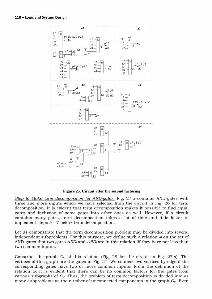
110 – Logic and System Design
a2
a5
a1
t1t2t3x8x7
y7 y9 y14 y15d3
&
1t1t3x5
&
x91t2x1 &1
x8x7
y13
d3
2 3 4
5
t1t2t3x4x9
y2 y10 y12d3
&
x3
6
t1t2t3
&
x4d37
t2t1
t3
&
x2d18
t3t2
&t1
x1
y1 y2 y3d110
2
a3t2t1
t3
&
x2d2 d3
y411
&
1x312
13
t1t2t3x4
x9
y5 y6
d2 d3
t1t2
x4
&
d231t3
t1t3
x3
&
x6
y10 y11 y12
d24
30
x9
a4
t2x1
&
&x9x3
x61
t2
1
&x5t2
x9
t1t3
& y7 y8 y9
20
22
24
21
23
2526&
x5x9
117
2
33x6&
x9
x3
2
132
Figure 25. Circuit after the second factoring
Step 8. Make term decomposition for AND-gates. Fig. 27,a contains AND-gates with three and more inputs which we have selected from the circuit in Fig. 26 for term decomposition. It is evident that term decomposition makes it possible to find equal gates and inclusion of some gates into other ones as well. However, if a circuit contains many gates, term decomposition takes a lot of time and it is faster to implement steps 5 – 7 before term decomposition. Let us demonstrate that the term decomposition problem may be divided into several independent subproblems. For this purpose, we define such a relation ω on the set of AND-gates that two gates ANDi and ANDj are in this relation iff they have not less than two common inputs. Construct the graph Gω of this relation (Fig. 28 for the circuit in Fig. 27,a). The vertices of this graph are the gates in Fig. 27. We connect two vertices by edge if the corresponding gates have two or more common inputs. From the definition of the relation ω, it is evident that there can be no common factors for the gates from various subgraphs of Gω. Thus, the problem of term decomposition is divided into as many subproblems as the number of unconnected components in the graph Gω. Even

Chapter 5 Multilevel and Multioutput Synthesis – 111
in our simple example, Gω contains five components and there are only 11 vertices (gates) in the largest component. For a complex FSM, the graph Gω contains a large number of components, since:
1. There is a large number of input variables in a complex FSM and there are not so many input variables in each row of its structure table (in each term corresponding to each row);
2. xi and x′i are different inputs of gates; 3. The number of gates and the number of inputs in each gate are decreased, as
a result of steps 4 – 7 (factoring, removal equal gates and inclusion of gates into other ones).
Figure 26. Circuit after the second removal equal gates
The result of term decomposition in our example is shown in Fig. 27,b. Fig. 29 contains the total circuit after this step.
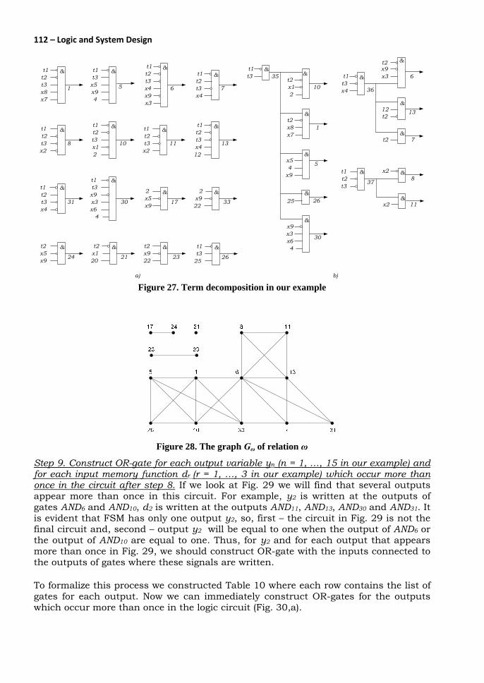
112 – Logic and System Design
t1t2t3x8x7
&
1
t1t3
x5
&
x94
5
t1t2t3x4x9
&
x3
6
t1t2t3
&
x47
t3t2
&t1
x12
10t2t1
t3
&
x28
&
12
13
t1t2t3x4
t1t2
x4
&
31t3
t2t1
t3
&
x211
t1t3
x3
&
x630
x9 &x5x9 17
4
2
33
&x9
2
22
t2x1
& &x9t2&
x5t2
x9
t1t3
&
20 2224 21 23 2625
t1t3
t2
x4
x9& x3
36
6
&12 13
t2t1
t3
&x28
&
37
&x2 11
&
x8x7
&
1
t2&
x12
10
t1t3
x5&
x94
5
35&
&26
x3
&
x6 30
x9
4
25
t2
a) b)
t2
&t2 7
Figure 27. Term decomposition in our example
Figure 28. The graph Gω of relation ω
Step 9. Construct OR-gate for each output variable yn (n = 1, …, 15 in our example) and for each input memory function dr (r = 1, …, 3 in our example) which occur more than once in the circuit after step 8. If we look at Fig. 29 we will find that several outputs appear more than once in this circuit. For example, y2 is written at the outputs of gates AND6 and AND10, d2 is written at the outputs AND11, AND13, AND30 and AND31. It is evident that FSM has only one output y2, so, first – the circuit in Fig. 29 is not the final circuit and, second – output y2 will be equal to one when the output of AND6 or the output of AND10 are equal to one. Thus, for y2 and for each output that appears more than once in Fig. 29, we should construct OR-gate with the inputs connected to the outputs of gates where these signals are written. To formalize this process we constructed Table 10 where each row contains the list of gates for each output. Now we can immediately construct OR-gates for the outputs which occur more than once in the logic circuit (Fig. 30,a).

Chapter 5 Multilevel and Multioutput Synthesis – 113
Figure 29. Logic circuit after term decomposition
Table 10. Gates for outputs
Step 10. Find equal OR-gates among the gates constructed at step 9. Leave only one gate in each set of equal gates. The logic circuit after removal of equal gates is shown in Fig. 30,b. Step 11. Find the inclusion of OR-gates into other gates among the gates constructed at steps 10. Unfortunately, we do not have any such cases in our rather simple example. Step 12. Make term decomposition for all OR-gates. Just as at Step 8 for AND-gates, we consider here only the gates with not less than three inputs since the minimal number of inputs in a common term in term decomposition is equal to two (after removal equal gates and full inclusion). Similar to step 8, we should construct the
Outputs Gates Outputs Gates Outputs Gates y1 e10 y7 e1 e26 y13 e5 y2 e6 e10 y8 e26 y14 e1 y3 e10 y9 e1 e26 y15 e1 y4 e11 y10 e6 e30 d1 e8 e10 y5 e13 y11 e30 d2 e11 e13 e30 e31 y6 e13 y12 e6 e30 d3 e1 e5 e6 e7 e11 e13

114 – Logic and System Design
graph of the relation ω for OR-gates. The problem of term decomposition for OR-gates is divided into as many subproblems as the number unconnected components in the graph of ω. In our rather simple example, we have only two OR-gates with more than two inputs (see d2 and d3 in Fig. 30,b).
Figure 30. OR-gates before (a) and after (b) removal equal gates
The final logic circuit is shown in Fig. 31. We have placed the circuit from Fig. 30,b at the bottom of Fig. 31. Of course, we should remove appearances of the outputs y2, y7, y9, y10, y12 and input memory functions d1, d2, d3 from other parts of the logic circuit. Thus, only the outputs that have one entry in the column “Gates” of Table 10 will be in the part of the circuit that is above the “OR for outputs and input memory functions” in Fig. 31. Step 13. Relax and drink your coffee. Really, the reason, that we cannot demonstrate gate inclusion and term decomposition for OR-gates, can be explained not only by the simplicity of our example, but also a very effective optimization at the previous steps that allows to decrease the number of inputs in the most gates of our circuit. To overcome some dissatisfaction of our last steps, let us discuss one more example, from the synthesis another FSM, presented in Table 11 and Fig. 32 with OR-gates for output variables and input memory functions which occur more than once in the circuit after Step 9.
Table 11. Gates for outputs in one more example
Step 10a. From Table 11 or Fig. 32 we immediately get that OR75 = OR68 and OR76 = OR67. We remove OR75 and OR76 and get y9 together with y6 from OR68 and y10 together with y5 from OR67 (Fig. 33).
Outputs Gates Outputs Gates y1 e5 e31 e36 e39 y8 e4 e44 y2 e3 e5 e36 y9 e16 e30 y3 e39 e56 e60 y10 e3 e16 e43 y4 e4 e31 e36 e42 d1 e56 e60 y5 e3 e16 e43 d2 e3 e4 e31 e36 e39 e44 y6 e16 e30 d3 e3 e4 e31 e42 e43 y7 e16 e44 e56 d4 e3 e4 e5 e42 e43 e44 e56
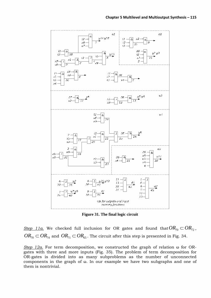
Chapter 5 Multilevel and Multioutput Synthesis – 115
Figure 31. The final logic circuit
Step 11a. We checked full inclusion for OR gates and found that 7270 OROR ⊂ ,
7470 OROR ⊂ and 6571 OROR ⊂ . The circuit after this step is presented in Fig. 34. Step 12a. For term decomposition, we constructed the graph of relation ω for OR-gates with three and more inputs (Fig. 35). The problem of term decomposition for OR-gates is divided into as many subproblems as the number of unconnected components in the graph of ω. In our example we have two subgraphs and one of them is nontrivial.

116 – Logic and System Design
Figure 32. OR-gates for yn and dr in one more example
Figure 33. OR-gate transformation after removal of equal gates
Figure 34. OR-gates after full inclusion
Figure 35. The graph of relation ω for OR-gates

Chapter 5 Multilevel and Multioutput Synthesis – 117
Figure 36. Logic circuit after term decomposition
The logic circuit after term decomposition is presented in Fig. 36. Its cost is 10 inputs lower than in the initial circuit in Fig. 32.

118 – Logic and System Design

Chapter 6 Transformation of Algorithmic State Machines
In this Chapter, we consider two more representations of Algorithmic State Machine – System of transition formulae and Matrix scheme of algorithms. After this, we will discuss transformation of Algorithmic State Machine – minimization of conditional and operator vertices and combining of Algorithmic State Machines. We will use these transformations in the next chapter dedicated to the high level synthesis of digital systems.
6.1 Various representations of Algorithmic State Machine 6.1.1 System of transition formulae. As an example, we use ASM Γ in Fig. 1. Let us look at operators following operator Yb. The facts that operator Y3 is implemented after Yb when x1x4x3 = 1, operator Y1 is implemented after Yb when x1x'4 = 1 and operator Y5 is implemented after Yb when x1x4x'3 = 1 or x'1 = 1, can be represented as the formula
Yb → x1x4x3Y3 + x1x4x'3Y5 + x1x'4Y1 + x'1Y5. (1)
Figure 1. ASM Γ
In general, the transition formula for the operator Yi is
∑+
=
→1
1
T
ttiti YY α , i = b, 1, …, T.
Here YT+1 = Ye is the operator, corresponding to the final vertex "End" and αit is the transition function from Yi to Yt (see Section 4.1.2 in Chapter 4). The term αitYt is equal to Yt if αit = 1, and is equal to 0 if αit = 0. The transition formulae can be transformed according to the rules of Boolean algebra and the following additional rules:
1. (α + β)Yi = αYi + βYi; 2. αβYi + αγYj = α(βYi + γYj); 3. If α = β then αYi = βYi.

120 – Logic and System Design
Here α, β and γ are Boolean functions and Yi and Yj are operators. The set of transition formulae for all i = b, 1, 2, . . ., T is called the system of transition formulae. This system contains seven formulae for ASM Γ in Fig. 1:
Yb → x1x4x3Y3 + x1x4x'3Y5 + x1x'4Y1 + x'1Y5; Y1 → x3Y2 + x'3Y4; Y2 → x6Ye; Y3 → x5x1Y6 + x5x'1Y2 + x'5Y2; (2) Y4 → x2Y1 + x'2Y3; Y5 → x4x3Y3 + x4x'3Y5 + x'4Y1; Y6 → Ye.
The following representation of the transition formula
Yi → xmA + x'mB (3) is called the expansion of transition formula Yi by variable xm. Here xm is one of the logical conditions and transition subformulae A and B do not depend on xm. For example, let us expand formula (1) by variable x1:
Yb → x1(x4x3Y3 + x4x'3Y5 + x'4Y1) + x'1Y5 . (4) If some terms of the transition formula do not depend on xm, then these terms must be multiplied by expression (xm + x'm) before the expansion of the transition formula by xm. Thus, any transition formula may be expanded by any variable. For example, expanding the transition formula (1) by the variable x4 we obtain
Yb → x1x4x3Y3 + x1x4x'3Y5 + x1x'4Y1 + x'1(x4 + x'4)Y5 = = x4(x1x3Y3 + x1x'3Y5 + x'1Y5) + x'4(x1Y1+ x'1Y5). (5)
In expression (3), we can continue expanding subformulae A and B by other variables until the terms in the internal brackets are as follows:
(xpYm+ x'pYn) (6) where Ym,Yn є { Y1, …, YT, YT+1}. This expression corresponds to subgraph G1 in Fig. 2. The resulting transition formula and the system of such formulae are called the bracket transition formula and the system of transition formulae in the bracket form correspondingly.
Figure 2. Subgraph G1 corresponding to expression (6)
Let us continue to expand the transition formula for Yb in expression (4):
Yb → x1(x4(x3Y3 + x'3Y5) + x'4Y1) + x'1Y5. (7) Expression (7) presents the transition formula for Yb in a bracket form. It is easy to show that there is a one-to-one correspondence between the bracket transition formula and the ASM subgraph obtained from this formula. To illustrate this,

Chapter 6 Transformation of Algorithmic State machines – 121
consider the construction of ASM subgraph G2 (Fig. 3,a) for transition formula Yb in (7).
Figure 3. Subgraphs G2 and G3 corresponding to expansions (7) and (8)
First, draw operator vertex Yb. Then construct conditional vertex with x1 and link its input with the output of operator Yb, since first we expanded transition formula Yb with this variable x1. Next, construct conditional vertex x4 and link its input with the output "1" of the preceding conditional vertex x1, since the expansion by the variable x4 is implemented in brackets just after x1. Further, construct operator vertex Y5 and link its input with the output ‘0’ of conditional vertex x1, as there are no expansions by any variables after x'1. In exactly the same way construct conditional vertex x3, link its input with the output "1" of vertex x4, and link the zero output of vertex x4 with operator vertex Y1 etc. Thus, at each step we have no alternative and can construct only one subgraph for a given bracket transition formula. The ASM subgraph G3 in Fig. 3,b is constructed in a similar way for another expansion (8) of the same unexpanded transition formula Yb in (1). We changed the order of variables in this expansion:
Yb → x4(x1x3Y3 + x1x'3Y5+ x'1Y5) + x'4(x1Y1+ x'1Y5) = = x4(x1(x3Y3 + x'3Y5) + x'1Y5) + x'4(x1Y1+ x'1Y5). (8)
Thus, to obtain a ASM subgraph from a bracket transition formula it is sufficient to construct chains of conditional vertices in accordance with a sequence of the transition formula expansion. As seen from Fig. 3,a and Fig. 3,b, the number of conditional vertices in the subgraph for some transition formula depends on the order of the expansion of this transition formula. Now it is evident that to transit from a system of transition formulae to ASM it is necessary to expand this system to the bracket form and to construct the ASM subgraph for each bracket transition formula. We will show now that the number of conditional vertices in the ASM, thus constructed, depends not only on the separate expansion of each transition formula but also on their joint expansion. Let us rewrite here expression (7) and expand transition formula for Y5 beginning from variable x4:
;))(( 5'11
'45
'33341 YxYxYxYxxxYb +++→ (7)
;)( 1'45
'33345 YxYxYxxY ++→ (9)

122 – Logic and System Design
For example, let us construct ASM subgraph G4 for bracket transition formulae Yb and Y5 in (7) and (9). The identical subformulae are underlined in these expressions. Obviously, one subgraph corresponds to the same subformulae so only one subgraph is constructed for these subformulae (Fig. 4,a).
Figure 4. Subgraphs G4 (a) and G5 (b) corresponding to expansions (7, 9) and (7, 10) Now we construct the ASM subgraph for the same bracket transition formula for Yb (7) and the new bracket transition formula Y5, obtained by its expansion beginning with variable x3:
Y5 → x3(x4Y3 + x'4Y1) + x'3(x4Y5+ x'4Y1). (10) Since there are no identical subformulae in bracket transition formulae (7) and (10) we derive subgraph G5 (Fig. 4,b) with three additional conditional vertices, compared to subgraph G4 in Fig. 4,a. At the end of this section, we expand the system of transition formulae, presented in (2):
;))(( 5'11
'45
'33341 YxYxYxYxxxYb +++→
;4'3231 YxYxY +→
Y x Y2 6→ e ; ;)( 2
'52
'16153 YxYxYxxY ++→ (11)
;3'2124 YxYxY +→
;)( 1'45
'33345 YxYxYxxY ++→
Y Y6 → e . 6.1.2. Matrix schemes of algorithms. The matrix scheme of algorithm (MSA) is a square matrix with rows Yb, Y1,. . ., YT, and columns Y1,Y2,. . ., YT, Ye. We write the transition function from operator Yi to operator Yj at the intersection of row Yi and column Yj in this matrix. The MSA M for ASM Г from Fig. 1 is presented in Table 1. For simplicity, we do not write the transition functions that are equal to zero in the matrix scheme of algorithm.

Chapter 6 Transformation of Algorithmic State machines – 123
The transition from ASM to MSA is obvious. We find all transition functions in ASM and place them into the corresponding entries of MSA. To transit from MSA to ASM we should obtain a system of transition formulae, a system of bracket transition formulae and then ASM. Just as for ASM (Section 4.1.3), it is possible to define an execution of MSA and a value of MSA for any sequence of vectors of logical conditions.
Table 1. MSA M
6.2 Minimization of conditional vertices in Algorithmic state machines
In this section, we will discuss minimization of conditional vertices in ASMs. The minimization algorithm consists of three steps. In the first step, the initial ASM is divided into such subgraphs G GQ1, ..., , that for obtaining the minimal ASM it is sufficient to minimize the number of conditional vertices in each subgraph independently of one another. In the second step, for each subgraph G q Qq( ,..., )=1
we will find a set of equivalent ones that contains the minimized subgraph Gqmin . In the
third step, the subgraph Gqmin will be obtained by solving the covering problem on the
set of subgraphs found in the second step. 6.2.1 ASM partitioning into subgraps. As an example for ASM minimization, we will use ASM Γnonmin in Fig. 5. To partition ASM, choose any operator, except the final oneYe , from the set of operators },,...,,{ 1 eTb YYYY and find the set of operators towards which there is a path
Y x x Yi i i iR j~ ... ~
1 (12)
from operator vertex Yi (i = b,1,2, …,T) passing only through conditional vertices with the logical conditions x xi iR1 , ... , . Here, as before, ~x xir ir= if the path proceeds
through the conditional vertex with xir via output ‘1’ ( , ... , )r R= 1 and irir xx '~ = if the path proceeds through the conditional vertex via output ‘0’. Since we can start from any operator, let us begin with the initial operator Yb. For ASM Γnonmin in Fig. 5, there are paths to Y1, Y4, Y5 from Yb. The arrows from operator Yb (Fig. 6,a) designate these paths. Next, go to the right side of this subgraph and find the operators, excludingYb , from which there are paths (12) leading to operatorsY Y Y1 4 5, , . We place these
operators ( , )Y Y2 3 under bY on the left side. For all operators on the left, continue finding such operators to which there are paths (12), etc., until the set on the left ( )A1 and that on the right ( )B1 are no longer increasing. Next, choose a new operator
Y1 Y2 Y3 Y4 Y5 Y6 Ye
Yb x1x'4 x1x4x3 x1x4x'3
x'1
Y1 x3 x'3 Y2 x6 Y3 x5x'1
x'5 x5x1
Y4 x2 x'2 Y5 x'4 x4x3 x4x'3 Y6 1
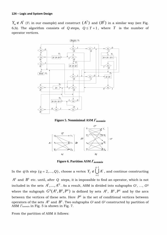
124 – Logic and System Design
Y Am ∉1 (Y1 in our example) and construct ( )A2 and ( )B2 in a similar way (see Fig.
6,b). The algorithm consists of Q steps, Q T≤ + 1 , where T is the number of operator vertices.
Begin
x3
0
x1
0
y1 y2 y3
x7
0
x2
0
x8
x2
1y4
x21
x11
x3
1 x6
y10 y11 y12
1
1
y2 y10 y121
0
0
y5 y60
x6 1
0
1
1
x3
1
y7 y8 y9 1x4
x5
x5
End
0
0
1
10
0
x81x2
0
0
0
1
1
0
0
Yb
Y1
Y2
Y3
Y4 Y5
Y6
Ye
Figure 5. Nonminimal ASM Γnonmin
Figure 6. Partition ASM Γnonmin
In the q th step ( , ... , )q Q= 2 , choose a vertex Y Afi
i
q
∉=
−
1
1
U , and continue constructing
Aq and Bq etc. until, after Q steps, it is impossible to find an operator, which is not
included in the sets A AQ1, ..., . As a result, ASM is divided into subgraphs G1, …, GQ
where the subgraph G A B Pq q q q( , , ) is defined by sets Aq , Bq , Pq and by the arcs
between the vertices of these sets. Here Pq is the set of conditional vertices between operators of the sets Aq and Bq . Two subgraphs G1 and G2 constructed by partition of ASM Γnonmin in Fig. 5 is shown in Fig. 7. From the partition of ASM it follows:

Chapter 6 Transformation of Algorithmic State machines – 125
1. For any two subgraphs G1 and G2: ∅=∩ ji AA ; ∅=∩ ji BB ; P Pi j∩ =∅.
2. The partition is independent of the choice of the first operator at every step. Since the partition is unique and the sets of conditional vertices in different subgraphs do not intersect ( P Pi j∩ =∅ ), the following statement results immediately:
R Rq
q
Q
==∑
1.
Here R is the number of conditional vertices in ASM and Rq is the number of conditional vertices in the subgraph Gq (q = 1, …, Q). In one of my previous works I
have proved that if ASM is partitioned into subgraphs G1, …, Gq and the number qRminof conditional vertices is minimal in each subgraph Gq (q = 1, …, Q), then the number of conditional vertices in ASM is also minimal and equal to
R Rq
q
Q
min min .==∑
1
Yb
x3 x11
x1
0
1
x6
1
Y5
1
Y4Y1
0
0 x3
Y2
1x6
0
x3
1
1
0
Y3
00
x7
Y1
0
x2
1
Y2
1
x2
x8
Y6
1
Ye
Y5
0
Y3
1
Y4
x4
x5
x5
1
0
Y6
x8
x2
0x2
1
11
0
00
0
1
0
1
0
a)
b)
Figure 7. Two subgraphs G1 and G2 as a result of partition of ASM Γnonmin
From the last statement, it follows that the problem of expansion for the system of transition formulae can be also divided into Q independent subproblems in accordance with the introduced partition of ASM. In our example for ASM Γnonmin, we have two such subsystems:
1. ;''''' 11341311346135613 YxxYxxYxxYxxxYxxxYb ++++→
;'' 434635632 YxYxxYxxY ++→ (13)
464365363 '' YxYxxYxxY ++→ .

126 – Logic and System Design
2. ;''''''' 82768272273272271 eYxxxYxxxYxxYxxYxxY ++++→
;'''''' 548546854543544 eee YxxYxxxYxxxYxxYxxY ++++→ (14)
;' 32225 YxYxY +→
.'''' 282286282286 eYxxYxxYxxYxxY +++→
6.2.2 Constructing a set of equivalent subgraphs. At this stage, we expand each subsystem of transition formulae, obtained at the previous stage, into the bracket form. To minimize a subgraph of ASM corresponding to the subsystem of transition formulae, M versions of expansion for each transition formula Yt should be constructed:
.'mimmimt BxAxY +→ (15)
Here x xi iM1 , ... , are the first M variables contained maximal times inYt . Then, we
again find M variables xnm and xpm which occur maximal times in Am and Bm . After
that, we continue expansion of Am and Bm with xnm and xpm :
).()( '''pmpmpmpmimnmnmnmnmimt FxExxDxCxxY +++→
Continuing expansion we get not more than MK2 1− version of expansion, here K is
the number of expansion levels. In our experiments with very complicated ASMs, we have seen that it is sufficient to take M K= = 3 so as not to lose the minimal subgraph of ASM. Now we return to our example and begin with transition formula Yb from the first subsystem (13). Let us find how many times each variable occurs in the transition formula forYb :
x1 – 5 times; x3 – 5 times; x6 – 2 times.
In our simple example we use M = 2 , that is we make four expansions for Yb – two starting from x1 and two starting from x3 (two variables with the maximal number of appearances in transition formula Yb). Let us begin with x1:
11434635631 ')''( YxYxYxxYxxxYb +++→ . Since the expansion after x'1 is impossible, find how many times each variable occurs in the transition formula after x1:
x3 – 3 times; x 6 - 2 times.
In our example, we choose x3, x6 and get two expansion versions with 1x in the first step. First of them is
1143465631 ')')'(( YxYxYxYxxxYb +++→ . (16)
The result of the second expansion with 6x after x1 is:
1146435361 ')')'(( YxYxYxYxxxYb +++→ . (17) Now let us return to Fig. 2. In this figure, we marked the input of the conditional vertex with xp by operatorYq . The following transition formula
Chapter 6 Transformation of Algorithmic State machines – 127
npmpq YxYxY '+→
corresponds to operator Yq in Fig. 2. We call Yq a derivative operator and denote it by
a circle to distinguish it from primary rectangular operatorsY Y Y Yb T e, , ... , ,1 in the graph of ASM. For expansion (16) we can write the following derivative operators beginning with the internal brackets:
465610 ' YxYxY +→ ;
4310311 ' YxYxY +→ ;
1111112 ' YxYxY +→ . Derivative operator Y12 coincides with operatorYb . We write the numbers of derivative operators over the corresponding opening brackets in (16):
11434656
10
3
11
1
12')')'(( YxYxYxYxxxYb +++→ (18)
and list these operators in the special Table 2. Operators 121110 ,, YYY are the first three operators in this table (we use number t instead of Yt in Table 2).
Table 2. The derivative operators for Yb, Y2, Y3
10 x6 5 4 16 x1 4 1 11 x3 10 4 17 x1 10 1 12 x1 11 1 18 x3 17 16 13 x3 5 4 19 x1 5 1 14 x6 13 4 20 x6 19 16 15 x1 14 1 21 x3 20 16
It is obvious that there is a one-to-one correspondence between the bracket transition formula and the ASM subgraph obtained from this formula. To illustrate this, consider the construction of ASM subgraph (Fig. 8) for transition formula Yb in (18). We see at once that such a construction is reduced to the successive exposure of derivative operators Y Y Y12 11 10, , from Table 2. It is possible to present expansion (18) or the subgraph in Fig. 8 as the first column in Table 3 (v1 means version1). The number of derivative operators in this column is equal to the number of conditional vertices in Fig. 8. For now, disregard the parenthesis in the columns of this table.
Figure 8. Subgraph for expression (18)

128 – Logic and System Design
Table 3. The table of versions for Yb, Y2, Y3
Yb Y2 Y3
v1 v2 v3 v4 v5 v6 v7 v8 12 15 18 21 (11) (14) (14) (11) (11) (14) 17 20 (10) (13) (13) (10) (10) (13) 16 19
(10) 16 Exactly in the same way, we implement expansion for each version of Yb, Y2,Y3:
11464353
13
6
14
1
15')')'(( YxYxYxYxxxYb +++→ ;
);'(')')'(( 1141
16
3114656
10
1
17
3
18YxYxxYxYxYxxxYb ++++→
)'('))'(')'(( 1141
16
31141
16
61151
19
6
20
3
21YxYxxYxYxxYxYxxxYb +++++→ ;
;')'( 434656
10
3
11
2 YxYxYxxY ++→
;')'( 464353
13
6
14
2 YxYxYxxY ++→
;')'( 464353
13
6
14
3 YxYxYxxY ++→
.')'( 434656
10
3
11
3 YxYxYxxY ++→ Having these expressions, we can complete the table for derivative operators (Table 2) and the table of versions (Table 3). The last table contains four versions for implementation of transition formulaYb , two versions for transition formula Y2 and
two versions for transition formulaY3 . In Table 3, the derivative operator for Yj is
enclosed in brackets if it appears at least in one version Y f jf ( )≠ . Obviously, having
chosen one version for each Y Yb , ,2 Y3 we obtain the subgraph of ASM for the first subsystem of transition formulae. The number of conditional vertices in such a subgraph is equal to the number of derivative operators (excluding similar ones) in the chosen versions. For example, having chosen versions 52 ,vv and v7 , we will obtain the subgraph with five conditional vertices (Fig. 9). To obtain the subgraph with a minimal number of conditional vertices in the case of m operators Y Ym1 , ... , , we have
to choose one version for each Yj so, that the total number of derivative operators should be minimal. We call this problem the problem of finding a minimal cover for the table of versions. The total number of possible subgraphs that can be constructed from such a table is equal to R Rm1× ×... . Here Rj is the number of versions for operatorYj . In our simple
example (Table 3), this number is equal to 4 2 2 16× × = . Without detailed explanations, we give expansions for the second subsystem (14) of transition formulae, the list of derivative operators (Table 4) and the table of versions (Table 5):
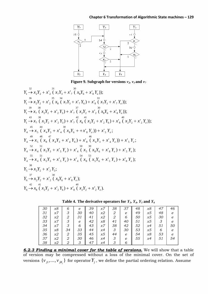
Chapter 6 Transformation of Algorithmic State machines – 129
Figure 9. Subgraph for versions v2, v5 and v7
));'('(' 868
30
737
31
222
32
1 eYxYxxYxxYxY +++→
));'(')'((' 737
33
86737
34
8
35
222
36
1 eYxYxxYxYxxxYxY ++++→
));'('(')'( 868
30
222
37
73222
38
7
39
1 eYxYxxYxxYxYxxY ++++→
));'(')'((')'( 222
40
86222
41
8
42
73222
38
7
43
1 eYxYxxYxYxxxYxYxxY +++++→
;'))'('( 5868
30
434
44
5
45
4 ee YxYxYxxYxxY ++++→
;'))'(')'(( 5434
46
86434
47
8
48
5
49
4 ee YxYxYxxYxYxxxY ++++→
);')'((')'( 5868
30
5
50
4535
51
4
52
4 eee YxYxYxxxYxYxxY ++++→
);')'((')'( 8565
53
8
54
4535
51
4
55
4 eee YxYxYxxxYxYxxY ++++→
;' 3222
38
5 YxYxY +→
);'(' 868
30
222
37
6 eYxYxxYxY ++→
).'(')'( 222
40
86222
41
8
42
6 eYxYxxYxYxxY +++→
Table 4. The derivative operators for Y1, Y4, Y5 and Y6
30 x8 6 e 39 x7 38 37 48 x8 47 46 31 x7 3 30 40 x2 2 e 49 x5 48 e 32 x2 2 31 41 x2 2 6 50 x5 30 e 33 x7 3 e 42 x8 41 40 51 x5 3 e 34 x7 3 6 43 x7 38 42 52 x4 51 50 35 x8 34 33 44 x4 3 30 53 x5 6 e 36 x2 2 35 45 x5 44 e 54 x8 53 e 37 x2 2 30 46 x4 3 e 55 x4 51 54 38 x2 2 3 47 x4 3 6
6.2.3 Finding a minimal cover for the table of versions. We will show that a table of version may be compressed without a loss of the minimal cover. On the set of versions { ,..., }v vj jRj1 for operatorYj , we define the partial ordering relation. Assume

130 – Logic and System Design
Table 5. The table of versions for Y1, Y4, Y5 and Y6
Y1 Y4 Y5 Y6 v1 v2 v3 v4 v5 v6 v7 v5 v6 v7 v8 32 36 39 43 45 49 52 55 (38) (37) (42) 31 35 (38) (38) 44 48 51 51 (30) (41) (30) 34 (37) (42) (30) 47 50 54 (40)
33 (30) (41) 46 (30) 53 (40)
that vs ≤ vt if the use of vs instead of vt does not increase the number of derivative operators in any cover of the table of versions. It is clear that if vs ≤ vt, version vt may be eliminated from the table of versions. It is easy to show that vs ≤ vt if two following conditions are true:
Ls ≤ Lt; (Lt - Ls) - |Bt \ Bs| ≥ 0.
Here, Lt and Ls are the lengths of versions vt and vs (the number of derivative operators in these versions); Bt and Bs are the sets of operators in brackets in versions vt and vs; |Bt \ Bs| is the number of elements in the difference between set Bt and Bs. Let us compare some versions from Table 3.
(a) v1 and v3: L1 = 3; L3 = 4; L1 < L3; (L3 – L1) - |B3 \ B1| = (4 – 3) - |{10} \ {11,10}| = 1 – 0 = 1 > 0;
v1 ≤ v3.
(b) v1 and v4: L1 = 3; L4 = 4; L1 < L4;
(L4 – L1) - |B4 \ B1| = (4 – 3) - |∅\ {11,10}| = 1 – 0 = 1 > 0;
v1 ≤ v4.
(c) v1 and v2: L1 = 3; L2 = 3; L1 = L2; (L2 – L1) - |B2 \ B1| = (3 – 3) - |{14,13} \ {11,10}| = 0 – 2 = -2 < 0; v1 not ≤ v2.
(d) Check the inverse: v2 and v1: L1 = 3; L2 = 3; L1 = L3;
(L1 – L2) - |B1 \ B2| = (3 – 3) - |{11,10} \ {14,13}| = 0 – 2 = -2 < 0;
v2 not ≤ v1; these two versions are incomparable.
(e) Versions (v5, v6) for Y2 and (v7, v8) for Y3 are incomparable as well (check it yourself).
The algorithm for compressing a table of versions is obvious. Comparing the versions within the columns for each Yj ( , ... , )j m= 1 , we leave only those versions that are not worse than the others. Thus, after such a compression, only incomparable versions will remain in the table of versions. Table 6, which is the result of the first compression, contains only two versions for Yb, Y2 and Y3.
Chapter 6 Transformation of Algorithmic State machines – 131
Table 6. The result of the first compression
Yb Y2 Y3 v1 v2 v5 v6 v7 v8 12 15 (11) (14) (14) (11) (11) (14) (10) (13) (13) (10) (10) (13)
If there is at least one common version for two operators, we can combine their versions and consider these two operators as one operator (see Table 7).
Table 7. Y2 and Y3 as one operator
Yb Y2,Y3 v1 v2 v5 v6 12 15 (11) (14) (11) (14) (10) (13) (10) (13)
The compression procedure should be repeated several times. If after the final compression more than one version is available for one or several operators Yj (j = 1, …, T) we can apply any well-known method to obtain a minimal cover for the prime implicant chart, because the complexity of the problem is essentially reduced. In our example, we can present the table of version in the sum-of-products form. For Table 7, we present each version as a product of its derivative operators and the set of version for each operator – as the sum-of-products:
(12*11*10 + 15*14*13) * (11*10 + 14*13) = = 12*11*10 + 15*14*13*11*10 + 12*11*10*11*10 + 15*14*13 = 12*11*10 + 15*14*13.
After absorption, we get two products with the same length equal to three. It means that after minimization, the number of derivative operators or, which is the same, the number of conditional vertices in the first subgraph is equal to three. We use the first product in the final Table 8. The minimal subgraph is presented in Fig. 10,a. The corresponding derivative operators are taken from Table 8.
Table 8. The minimal cover of the table of versions
Yb Y2,Y3 v1 v3 12 (11) (11) (10) (10)
Without detailed explanations, we will present the process of minimization for subgraph G2. Table 9 contains the results of the first compressing of the table of versions. The next compressing is not possible, so we use sum-of-products to find a minimal subgraph: (32*31*30 + 39*38*37*30 + 43*38*42*41*40) * (45*44*30) * (38) * (37*30 + 42*41*40) = = (32*31*30 + 39*38*37*30 + 43*38*42*41*40) * (45*44*30*38*37 + 45*44*30*38*42*41*40)= = 32*31*30*45*44*38*37 + 32*31*30*45*44*38*42*41*40 + 39*38*37*30*45*44 + + 39*38*37*30*45*44*42*41*40 + 43*38*42*41*40*45*44*30*37 + 43*38*42*41*40*45*44*30 = 45*44*38*37*32*31*30 + 45*44*42*41*40*38*32*31*30 +
+ 45*44*39*38*37*30 + 45*44*43*42*41*40*38*30.
132 – Logic and System Design
Figure 10. Subgraphs G1 and G2 after minimization
After absorption we get four products, the third of them contains the minimal number (six) of derivative operators. The final cover of the table of versions for the second subgraph G2 is shown in Table 10. The minimal subgraph G2 is shown in Fig. 10,b. The minimized ASM Γmin is presented in Fig. 11. It contains only 9 conditional vertices whereas ASM Γnonmin in Fig. 5 has 17 conditional vertices.
Table 9. The result of the first compression
Y1 Y4 Y5 Y6
v1 v3 v4 v5 v6 v7 v8 32 39 43 45 (38) (37) (42) 31 (38) (38) 44 (30) (41) (30) (37) (42) (30) (40)
(30) (41) (40)
Table 10. The minimal cover of the table of versions
Y1 Y4 Y5 Y6 v3 v5 v6 v7 39 45 (38) (37) (38) 44 (30) (37) (30) (30)

Chapter 6 Transformation of Algorithmic State machines – 133
Figure 11. Mimimized ASM minΓ 6.3. Minimization of operator vertices
We will show that to minimize the number of operator vertices in ASM it is necessary to construct a Moore FSM implementing the given ASM, minimize this FSM and return from the minimal FSM to the minimal ASM. Thus, the minimization of operator vertices in ASM is reduced to the minimization of the corresponding Moore FSM. We will illustrate this technique by means of example of nonminimal ASM in Fig. 12. As was shown in Chapter 4 (Section 4.3), Moore FSM can be synthesized in two steps:
1. The construction of a marked ASM. At this step, the vertices Begin and End are marked by the same symbol a1 and all operator vertices are marked by symbols a2, …, aM. These marks are written in Fig. 12 near the corresponding vertices. Unlike to the marking in Chapter 4, we use symbol ae to mark vertex End to distinguish the beginning and final vertices while returning from the minimal FSM to the minimal ASM.
2. To define the transitions in FSM Moore with the states a1, …, aM, ae we find the following transition paths between operator vertices in the marked ASM:
smRmm axxa ~...~1 .
Here mrmr xx =~ if in the transition path, we leave the conditional vertex with
mrx via output ‘1’ and mrmr xx '~ = if we leave the vertex with mrx via output ‘0’.
The transition from state am to state as with input X(am, as) = mRm xx ~...~
1 corresponds to such a path. If am marks the operator vertex with operator Yt, then the output function λ(am) = Yt, i.e. we identify operator Yt, written in the operator vertex with this state am.
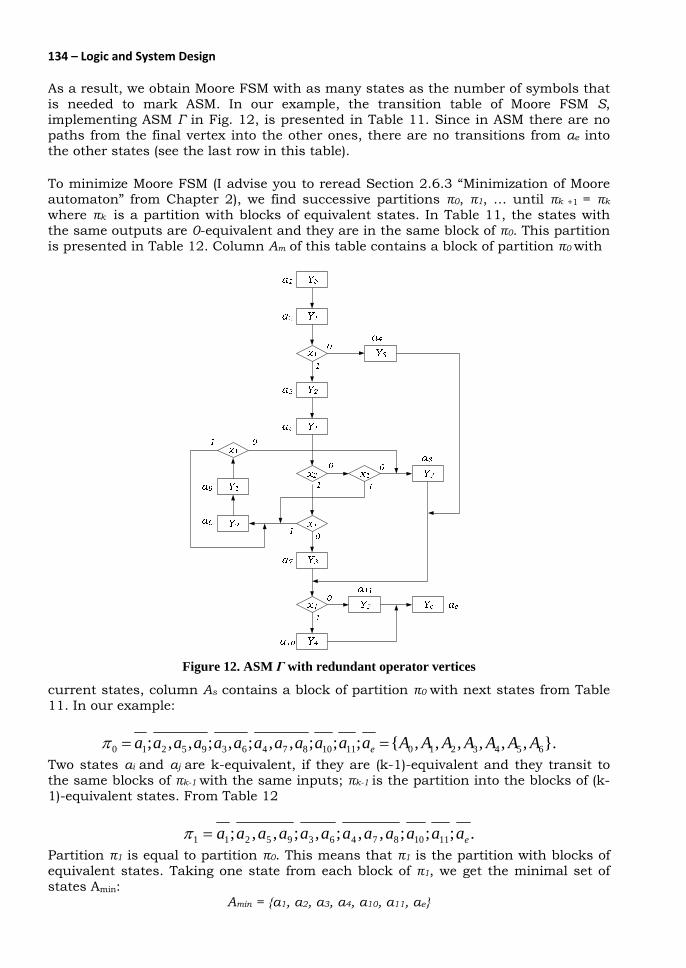
134 – Logic and System Design
As a result, we obtain Moore FSM with as many states as the number of symbols that is needed to mark ASM. In our example, the transition table of Moore FSM S, implementing ASM Γ in Fig. 12, is presented in Table 11. Since in ASM there are no paths from the final vertex into the other ones, there are no transitions from ae into the other states (see the last row in this table). To minimize Moore FSM (I advise you to reread Section 2.6.3 “Minimization of Moore automaton” from Chapter 2), we find successive partitions π0, π1, … until πk +1 = πk where πk is a partition with blocks of equivalent states. In Table 11, the states with the same outputs are 0-equivalent and they are in the same block of π0. This partition is presented in Table 12. Column Am of this table contains a block of partition π0 with
Figure 12. ASM Γ with redundant operator vertices
current states, column As contains a block of partition π0 with next states from Table 11. In our example:
}.,,,,,,{;;;,,;,;,,; 654321011108746395210 AAAAAAAaaaaaaaaaaaa e ==π Two states ai and aj are k-equivalent, if they are (k-1)-equivalent and they transit to the same blocks of πk-1 with the same inputs; πk-1 is the partition into the blocks of (k-1)-equivalent states. From Table 12
.;;;,,;,;,,; 11108746395211 eaaaaaaaaaaaa=π Partition π1 is equal to partition π0. This means that π1 is the partition with blocks of equivalent states. Taking one state from each block of π1, we get the minimal set of states Amin:
Amin = {a1, a2, a3, a4, a10, a11, ae}

Chapter 6 Transformation of Algorithmic State machines – 135
and the minimal Moore FSM (Table 13). It is clear that minimal ASM Γmin contains one beginning vertex (state a1), one final vertex (state ae) and five operator vertices (states a2, a3, a4, a10 and a11). To construct this minimal ASM we should divide the system of transition formulae into subsystems – we have four such subsystems in our example (Fig. 13) – and transform each subsystem into the bracket form:
1. 1YY b → ; ;12 YY →
2. ;' 31211 YxYxY +→
3. ;' 54443 YxYxY +→
4. eYY →4 ; .5 eYY →
ASM Γmin with the minimal number of operator vertices (Fig. 14) was constructed by means of this system of bracket transition formulae.
Table 13. The minimal Moore FSM
am Y(am) as X(am, as) h a1 Yb a2 1 1 a2 Y1 a3 x1 2 a4 x'1 3
a3 Y2 a2 1 4 a4 Y3 a10 x4 5 a11 x'4 6
a10 Y4 ae 1 7 a11 Y5 ae 1 8 ae Ye ae 1 9
Table 12. Partition π0
Am am Y(am) As X(am, as) A0 a1 Yb A1 1 a2 Y1 A2 x1 A3 x'1
A1 a5 Y1 A2 x2x1 A3 x2x'1 A2 x'2x1 A3 x'2x'1 a9 Y1 A2 x1 A3 x'1
A2 a3 Y2 A1 1 a6 Y2 A1 1 a4 Y3 A4 x4 A5 x'4
A3 a7 Y3 A4 x4 A5 x'4 a8 Y3 A4 x4 A5 x'4
A4 a10 Y4 A6 1 A5 a11 Y5 A6 1 A6 ae Ye A6 1
Table 11. FSM Moore for ASM Γ
am Y(am) as X(am, as) h a1 Yb a2 1 1 a2 Y1 a3 x1 2 a4 x'1 3
a3 Y2 a5 1 4 a4 Y3 a10 x4 5 a11 x'4 6
a5 Y1 a6 x2x1 7 a7 x2x'1 8 a6 x'2x1 9 a8 x'2x'1 10
a6 Y2 a9 1 11 a7 Y3 a10 x4 12 a11 x'4 13
a8 Y3 a10 x4 14 a11 x'4 15
a9 Y1 a6 x1 16 a8 x'1 17
a10 Y4 ae 1 18 a11 Y5 ae 1 19 ae Ye ae 1 20
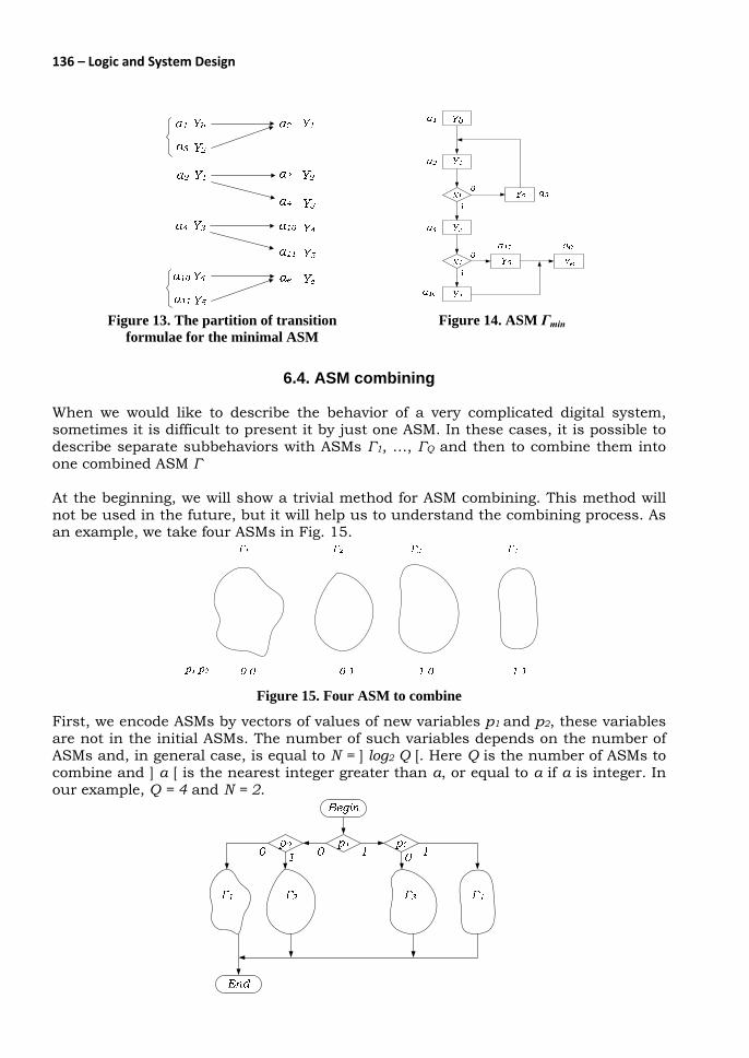
136 – Logic and System Design
6.4. ASM combining
When we would like to describe the behavior of a very complicated digital system, sometimes it is difficult to present it by just one ASM. In these cases, it is possible to describe separate subbehaviors with ASMs Γ1, …, ΓQ and then to combine them into one combined ASM Γ At the beginning, we will show a trivial method for ASM combining. This method will not be used in the future, but it will help us to understand the combining process. As an example, we take four ASMs in Fig. 15.
Figure 15. Four ASM to combine
First, we encode ASMs by vectors of values of new variables p1 and p2, these variables are not in the initial ASMs. The number of such variables depends on the number of ASMs and, in general case, is equal to N = ] log2 Q [. Here Q is the number of ASMs to combine and ] a [ is the nearest integer greater than a, or equal to a if a is integer. In our example, Q = 4 and N = 2.
Figure 14. ASM Γmin
Figure 13. The partition of transition
formulae for the minimal ASM
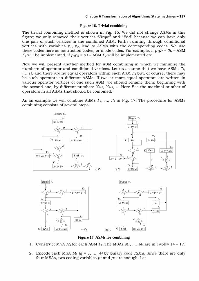
Chapter 6 Transformation of Algorithmic State machines – 137
Figure 16. Trivial combining
The trivial combining method is shown in Fig. 16. We did not change ASMs in this figure; we only removed their vertices “Begin” and “End” because we can have only one pair of such vertices in the combined ASM. Paths running through conditional vertices with variables p1, p2, lead to ASMs with the corresponding codes. We use these codes here as instruction codes, or mode codes. For example, if p1p2 = 00 – ASM Γ1 will be implemented, if p1p2 = 01 – ASM Γ2 will be implemented etc. Now we will present another method for ASM combining in which we minimize the numbers of operator and conditional vertices. Let us assume that we have ASMs Γ1, …, ΓQ and there are no equal operators within each ASM Γq but, of course, there may be such operators in different ASMs. If two or more equal operators are written in various operator vertices of one such ASM, we should rename them, beginning with the second one, by different numbers YF+1, YF+2, … Here F is the maximal number of operators in all ASMs that should be combined. As an example we will combine ASMs Γ1, …, Γ4 in Fig. 17. The procedure for ASMs combining consists of several steps.
Begin
0
1x7
0x1
Y1
y1 y2 y3
1
y5 y6Y3
10x6
01 x3
Y4
y7 y8 y9
Y5
y10 y11 y12
Y6
y2 y10 y12
1
0x2
10x5
End Ye
Yb
Begin
0
1x60
1x3
Y4
y7 y8 y9
Y5
y10 y11 y12
Y6
y2 y10 y12
1
0x2
1
0x5
EndYe
Yb
y5 y6
Y3
10 x1
Begin
0
1x60
1x3
Y4
y7 y8 y9
Y5
y10 y11 y12
Y6
y2 y10 y12
1
0x2
1
0x5
EndYe
Yb
y5 y6
Y3
10 x1
y4
Y2
BeginY1
y1 y2 y3
y4Y2
10x6
01 x3
Y4
y7 y8 y9
y10 y11 y12
Y6
y2 y10 y12
10x2
10x5
EndYe
Y5
y5 y6
Y3
10 x1
Yb
b) Γ2 a) Γ1
d) Γ4 c) Γ3 Figure 17. ASMs for combining
1. Construct MSA Mq for each ASM Γq. The MSAs M1, …, M4 are in Tables 14 – 17.
2. Encode each MSA Mq (q = 1, …, 4) by binary code K(Mq). Since there are only four MSAs, two coding variables p1 and p2 are enough. Let
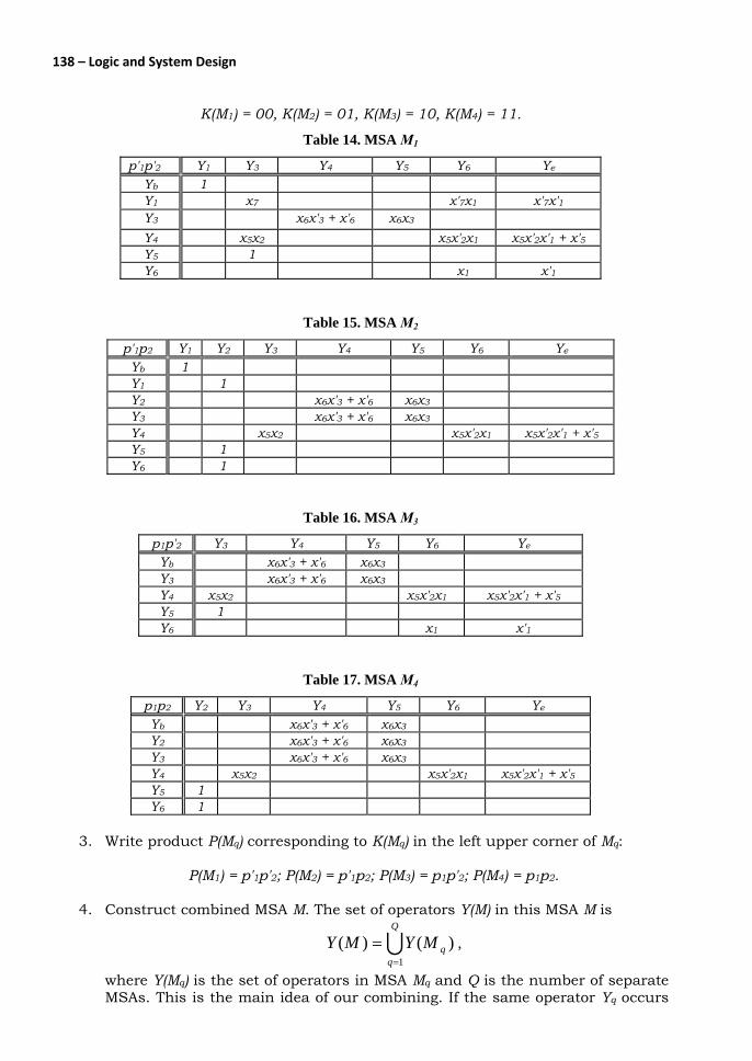
138 – Logic and System Design
K(M1) = 00, K(M2) = 01, K(M3) = 10, K(M4) = 11.
Table 14. MSA M1
Table 15. MSA M2
Table 16. MSA M3
Table 17. MSA M4
3. Write product P(Mq) corresponding to K(Mq) in the left upper corner of Mq:
P(M1) = p'1p'2; P(M2) = p'1p2; P(M3) = p1p'2; P(M4) = p1p2.
4. Construct combined MSA M. The set of operators Y(M) in this MSA M is
UQ
qqMYMY
1
)()(=
= ,
where Y(Mq) is the set of operators in MSA Mq and Q is the number of separate MSAs. This is the main idea of our combining. If the same operator Yq occurs
p′1p′2 Y1 Y3 Y4 Y5 Y6 Ye
Yb 1 Y1 x7 x′7x1 x′7x′1 Y3 x6x′3 + x′6 x6x3 Y4 x5x2 x5x′2x1 x5x′2x′1 + x′5 Y5 1 Y6 x1 x′1
p′1p2 Y1 Y2 Y3 Y4 Y5 Y6 Ye
Yb 1 Y1 1 Y2 x6x′3 + x′6 x6x3 Y3 x6x′3 + x′6 x6x3 Y4 x5x2 x5x′2x1 x5x′2x′1 + x′5 Y5 1 Y6 1
p1p′2 Y3 Y4 Y5 Y6 Ye
Yb x6x′3 + x′6 x6x3 Y3 x6x′3 + x′6 x6x3 Y4 x5x2 x5x′2x1 x5x′2x′1 + x′5 Y5 1 Y6 x1 x′1
p1p2 Y2 Y3 Y4 Y5 Y6 Ye
Yb x6x′3 + x′6 x6x3 Y2 x6x′3 + x′6 x6x3 Y3 x6x′3 + x′6 x6x3 Y4 x5x2 x5x′2x1 x5x′2x′1 + x′5 Y5 1 Y6 1

Chapter 6 Transformation of Algorithmic State machines – 139
in the several ASMs, there will be only one copy of this operator in the combined ASM. In our example: Y(M1) = {Yb, Y1, Y3, Y4, Y5, Y6, Ye}; Y(M2) = {Yb, Y1, Y2, Y3, Y4, Y5, Y6, Ye}; Y(M3) = {Yb, Y3, Y4, Y5, Y6, Ye}; Y(M4) = {Yb, Y2, Y3, Y4, Y5, Y6, Ye}. Thus, in our example we have only eight operators in the combined ASM, including operators Yb and Ye:
Y(M) = Y(M1) U Y(M2) U Y(M3) U Y(M4) = { Yb,Y1, …, Y6,Ye}.
This combined ASM has seven rows and seven columns (Table 18).
To construct entries in the combined MSA M, we multiply each entry of each MSA Mq by its product P(Mq) written in the left upper corner of this MSA Mq and insert it in the corresponding entry of MSA M – at the intersection of the same row and the same column. In other words, we multiply each MSA Mq by its product P(Mq) and insert it in the combined MSA M.
To check that combined MSA M, thus constructed, implements MSA Mq when P(Mq) = 1, it is sufficient to substitute code K(Mq) in each entry of MSA M. For example, if you substitute K(M1) = 00 in MSA M in Table 18, you will get MSA M1 in Table 14.
Table 18. Combined MSA M
Y1 Y2 Y3 Y4 Y5 Y6 Ye
Yb p′1p′2 p1p′2x6x′3 + p1p′2x′6 p1p′2x6x3 p′1p2 p1p2x6x′3 + p1p2x′6 p1p2x6x3
Y1 p′1p2 p′1p′2x7 p′1p′2x′7x1 p′1p′2x′7x′1
Y2 p′1p2x6x′3 + p′1p2x′6 p′1p2x6x3 p1p2x6x′3 + p1p2x′6 p1p2x6x3 p′1p′2x6x′3 + p′1p′2x′6 p′1p′2x6x3
Y3 p′1p2x6x′3 + p′1p2x′6 p′1p2x6x3 p1p′2x6x′3 + p1p′2x′6 p1p′2x6x3 p1p2x6x′3 + p1p2x′6 p1p2x6x3 p′1p′2x5x2 p′1p′2x5x′2x1 p′1p′2x5x′2x′1 + p′1p′2x′5
Y4 p′1p2x5x2 p′1p2x5x′2x1 p′1p2x5x′2x′1 + p′1p2x′5 p1p′2x5x2 p1p′2x5x′2x1 p1p′2x5x′2x′1 + p1p′2x′5 p1p2x5x2 p1p2x5x′2x1 p1p2x5x′2x′1 + p1p2x′5
Y5 p′1p2 p′1p′2 p1p2 p1p′2
Y6 p′1p2 p′1p′2x1 p′1p′2x′1
p1p2 p1p′2x1 p1p′2x′1
5. Construct combined ASM Γ.
5.1. Partition the system of transition formulae into independent subsystems. Here we should implement techniques similar to ASM partitioning into subgraphs (Secion 6.2.1). We begin with any operator, for example, from Yb and find the set of operators towards which there are paths (12) in MSA M (the columns with entries distinct from zero in row Yb). For row Yb, they are operators Y1, Y4, Y5 (see arrows from Yb in Fig. 18,a). Next, we go to the right side of this subgraph and find operators, other than Yb, from which there are paths (12) leading to operators Y1, Y4, Y5. We place these operators (Y2, Y3) on the left side under Yb. For all operators on the left, we continue picking such

140 – Logic and System Design
operators to which there are paths in MSA M, etc., until the set on the left (А1) and that on the right (B1) are no longer increasing. Next we will choose a new operator Y Am ∉ 1 (Y1 in our example) and construct (A2) and (B2) in a similar way (see Fig. 18,b). Thus, in our example we have two independent subsystems of transition formulae derived immediately from MSA M:
Figure 18. Partition of operators in MSA M
Subsystem 1 Yb → p'1p'2Y1 + p'1p2Y1 + p1p'2x6x'3Y4 + p1p'2x'6Y4 + p1p2x6x'3Y4 + p1p2x'6Y4 + p1p'2x6x3Y5 + p1p2x6x3Y5; Y2 → p'1p2x6x'3Y4 + p'1p2x'6Y4 + p1p2x6x'3Y4 + p1p2x'6Y4 + p'1p2x6x3Y5 + p1p2x6x3Y5; Y3 → p'1p'2x6x'3Y4 + p'1p'2x'6Y4 + p'1p2x6x'3Y4 + p'1p2x'6Y4 + p1p'2x6x'3Y4 + p1p'2x'6Y4 + p1p2x6x'3Y4 + p1p2x'6Y4 + p'1p'2x6x3Y5 + p'1p2x6x3Y5 + p1p'2x6x3Y5 + p1p2 x6x3Y5. Subsystem 2 Y1 → p'1p2Y2 + p'1p'2x7Y1 + p'1p'2x'7x1Y6 + p'1p'2x'7x'1Ye; Y4 → p'1p'2x5x2Y3 + p'1p2x5x2Y3 + p1p'2x5x2Y3 + p1p2x5x2Y3 + p'1p'2x5x'2x1Y6 + p'1p2x5x'2x1Y6 + p1p'2x5x'2x1Y6 + p1p2x5x'2x1Y6 + p'1p'2x5x'2x'1Ye + p'1p'2x'5Ye + p'1p2x5x'2x'1Ye + p'1p2x'5Ye + p1p'2x5x'2x'1Ye + p1p'2x'5Ye + p1p2x5x'2x'1Ye + p1p2x'5Ye; Y5 → p'1p2Y2 + p1p2Y2 + p'1p'2Y3 + p1p'2Y3;
Y6 → p'1p2Y2 + p1p2Y2 + p'1p'2x1Y6 + p1p'2x1Y6 + p'1p'2x'1Ye + p1p'2x'1Ye.
5.2. Construct minimal subgraphs. Here we should implement techniques presented above in Section 6.2.2 “Constructing a set of equivalent subgraphs” and Section 6.2.3 “Finding a minimal cover for the table of versions”. Without detailed explanation (we advice you to make ASM expansion by yourself) we give the tables of derivative operators for the first subsystem (Table 19) and the tables of versions during two compressions (Tables 20 and 21). The minimal subgraph with operators Yb, Y2 and Y3 is presented in Table 22.
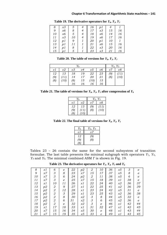
Chapter 6 Transformation of Algorithmic State machines – 141
Table 19. The derivative operators for Yb, Y2, Y3
8 x3 5 4 16 p1 4 1 9 x6 8 4 17 x3 15 16
10 x6 5 4 18 x6 14 16 11 x3 10 4 19 x6 17 16 12 p1 9 1 20 p1 10 1 13 p1 11 1 21 x6 15 16 14 p1 8 1 22 x3 20 16 15 p1 5 1 23 x3 21 16
Table 20. The table of versions for Yb, Y2, Y3
Yb Y2, Y3
v1 v2 v3 v4 v5 v6 v7 v8 12 13 18 19 22 23 (9) (11) (9) (11) 14 17 20 21 (8) (10) (8) (10) (8) 15 (10) 15 16 16 16 16
Table 21. The table of versions for Yb, Y2, Y3 after compression of Yb
Yb Y2, Y3
v1 v2 v7 v8 12 13 (9) (11) (9) (11) (8) (10) (8) (10)
Table 22. The final table of versions for Yb, Y2, Y3
Yb Y2, Y3 v1 v7 12 (9) (9) (8) (8)
Tables 23 – 26 contain the same for the second subsystem of transition formulae. The last table presents the minimal subgraph with operators Y1, Y4, Y5 and Y6. The minimal combined ASM Γ is shown in Fig. 19.
Table 23. The derivative operators for Y1, Y4, Y5 and Y6
8 x1 6 е 22 p2 2 10 36 x5 3 е 9 x7 3 8 23 x7 15 17 37 x5 8 е
10 x7 3 6 24 p2 2 11 38 x5 6 е 11 x7 3 е 25 x7 15 18 39 x1 38 е 12 x1 10 11 26 x1 22 24 40 x2 36 37 13 p2 2 9 27 x1 22 25 41 x2 36 39 14 p2 2 12 28 x1 23 24 42 x5 31 е 15 p2 2 3 29 x1 23 25 43 x2 36 38 16 p2 2 8 30 x2 3 8 44 x5 32 е 17 p2 2 6 31 x2 3 6 45 x2 36 е 18 p2 2 е 32 x2 3 е 46 x1 42 44 19 x1 17 18 33 x1 31 32 47 x1 42 45 20 x7 15 16 34 x5 30 е 48 x1 43 44 21 x7 15 19 35 x5 33 е 49 x1 43 45

142 – Logic and System Design
Table 24. The table of versions for Y1, Y4, Y5 and Y6
Y1 Y4 Y5 Y6 v1 v2 v3 v4 v5 v6 v7 v8 v9 v10 v11 v12 v13 v14 v15 13 14 20 21 26 34 35 40 41 46 47 49 (15) (16) (19) 9 12 (15) (15) 22 30 33 36 36 42 42 43 (8) (17) (8) 10 (16) (19) 10 (8) 31 37 39 31 31 36 (18) 11 (8) (17) 24 32 (8) 38 44 45 38 (18) 11 32 36 45
Table 25. The compressed table of versions for Y1, Y4, Y5 and Y6
Y1 Y4 Y5 Y6 v1 v3 v4 v6 v13 v14 v15 13 20 21 34 (15) (16) (19) 9 (15) (15) 30 (8) (17) (8) (16) (19) (8) (18) (8) (17) (18)
Table 26. The final table of versions for Y1, Y4, Y5 and Y6
Y1 Y4 Y5 Y6 v3 v6 v13 v14 20 34 (15) (16) (15) 30 (8) (16) (8) (8)
Note, that during expansion of transition formulae we can come across two don't care cases:
• If the number of ASMs Q is smaller than 2N, i.e. not all possible vectors of coding variables p1, …, pN are used for encoding of MSAs M1, …, MQ, all transition formulae are not specified on such vectors of variables p1, …, pN,x1, …,xL, in which first N components correspond to unused combination. We do not have such a case in our example.
• If operator Yt is absent in some MSA Mq, then transition formula for Yt is not specified on vectors of variables p1, …, pN, x1, …, xL, in which first N components correspond to the code K(Mq) of this MSA Mq. The operator Y2 is not in MSAs M1 and M3 in our example, therefore the transition formula for Y2 is not specified for vectors, in which p1 = p2 = 0 and p1 = 1, p2 = 0, since K(M1) = 00 and K(M3) = 10.
Y2 → p'1p2x6x'3Y4 + p'1p2x'6Y4 + p1p2x6x'3Y4 + p1p2x'6Y4 + p'1p2x6x3Y5 + p1p2x6x3Y5 = = x6(p'1p2x'3Y4 + p1p2x'3Y4 + p'1p2x3Y5 + p1p2x3Y5) + x'6(p'1p2Y4 + p1p2Y4) = = x6(x3(p'1p2Y5 + p1p2Y5) + x'3(p'1p2Y4 + p1p2Y4)) + x'6(p'1p2Y4 + p1p2Y4). In the internal brackets, we couldn’t continue expanding with variable p2, because this expression does not contain products with p′1p′2 and p1p′2 corresponding to the unused codes 00 and 10. Using don’t care we have
p′1p2 + p′1p′2 = p′1; p1p2 + p1p′2 = p1

Chapter 6 Transformation of Algorithmic State machines – 143
and finally we get:
Y2 → x6(x3(p'1Y5 + p1Y5) + x'3(p'1Y4 + p1Y4)) + x'6(p'1Y4 + p1Y4) =
= x6(x3Y5 + x'3Y4) + x'6Y4.
Begin
p1 x61 0x2 Y4
Y1
0
x7 p21
p2
0
Y3
1
x5
x3
Y5
1
x1 0
Y6
End
0
1
0
1
1
0
1
Y2
1
0
0
Figure 19. Combined ASM Γ

144 – Logic and System Design
Related Documents