24 CHAPTER 3 QCA INTRODUCTION Quantum dot cellular automata provide a novel electronics paradigm for information processing and communication. It has been recognized as one of the revolutionary nanoscale computing devices. A major advantage of QCA over other nanoelectronic architectural styles is that the same cells that are used for making logic gates can be used to build wires carrying logic signals. The QCA allows operating frequencies in range of THz and device integration densities about 900 times more than the current end of CMOS scaling limits, which is not possible in current CMOS technologies. It has been predicted as one of the future nanotechnologies in Semiconductor Industries Association’s International Roadmap for Semiconductors (ITRS).Logical operations and data movement are accomplished via Coulombic interaction between neighbouring QCA cells rather than current flow. The QCA design involves diverse new paradigms such as memory- in-motion and processing-by-wire. Memory-in-motion is an instance of the more general paradigm of processing-by-wire. Processing-by-wire (PBW) is the QCA capability by which information manipulation can be accomplished, while transmission and communication of signals take place. PBW capabilities can be observed in the so-called inverter chain as well as in the arrangement of the cells in an MV.

Welcome message from author
This document is posted to help you gain knowledge. Please leave a comment to let me know what you think about it! Share it to your friends and learn new things together.
Transcript

� 24
CHAPTER 3
QCA INTRODUCTION
Quantum dot cellular automata provide a novel electronics
paradigm for information processing and communication. It has been
recognized as one of the revolutionary nanoscale computing devices. A major
advantage of QCA over other nanoelectronic architectural styles is that the
same cells that are used for making logic gates can be used to build wires
carrying logic signals. The QCA allows operating frequencies in range of THz
and device integration densities about 900 times more than the current end of
CMOS scaling limits, which is not possible in current CMOS technologies. It
has been predicted as one of the future nanotechnologies in Semiconductor
Industries Association’s International Roadmap for Semiconductors
(ITRS).Logical operations and data movement are accomplished via
Coulombic interaction between neighbouring QCA cells rather than current
flow.
The QCA design involves diverse new paradigms such as memory-
in-motion and processing-by-wire. Memory-in-motion is an instance of the
more general paradigm of processing-by-wire. Processing-by-wire (PBW) is
the QCA capability by which information manipulation can be accomplished,
while transmission and communication of signals take place. PBW
capabilities can be observed in the so-called inverter chain as well as in the
arrangement of the cells in an MV.

� 25
Quantum dots are nanostructures created from standard semi
conductive materials such as InAs/GaAs. These structures can be modeled as
3-dimensional quantum wells. As a result, they exhibit energy quantization
effects even at distances several hundred times larger than the material system
lattice constant.
A quantum dot can indeed be visualized as a well. Electrons, once
trapped inside the dot, do not alone possess the energy required to escape. We
can use quantum physics to our advantage because the smaller a quantum dot
is physically, the higher the potential energy necessary for an electron to
escape. The Figure 3.1 below shows an example of a quantum dot given by
Konard walus et al (2004).
Figure 3.1 Example quantum dot pyramid created with InAs/GaAs
3.1 QCA CELL
The fundamental unit in QCA circuits is a QCA cell which consists
of four quantum dots which are arranged in a square pattern as shown in
Figure 3.2. Zhang et al (2004) have stated the cell is charged with two excess
electrons which can be allowed to tunnel between the different quantum dots
by a clocking mechanism. These electrons tend to occupy the antipodal sites
as a result of their mutual electrostatic repulsion. The columbic repulsion is

� 26
responsible for the transfer of information from one cell to an adjacent cell.
Thus, there exist two equivalent energetically minimal arrangements of the
two electrons in the QCA cell as shown in Figure 3.2. These two
arrangements are denoted as cell polarization P= +1and P= -1.By using cell
polarization P =+1 to represent logic “1” and P =-1 to represent logic “0,”
binary information is encoded in the charge configuration of the QCA cell.
Also there are special purpose rotated cells. The regular cell and the rotated
cell don't interact with each other when they are aligned, so rotated cells can
be used for coplanar wire crossings.
Figure 3.2 Basic QCA cell and two possible polarizations
In QCA design, the cells are arranged systematically to implement
the desired gate and interconnect structures. The QCA designs are typically
analyzed using detailed cell to cell interactions.
The bounding box shown around the cell is used only to identify
one cell from another; they do not represent any physical system. Because the
electrons are quantum mechanical particles they are able to tunnel between
the dots in a cell. The electrons in cells placed adjacent to each other will
interact. As a result, the polarization of one cell will be directly affected by
the polarization of its neighbouring cells. This interaction is shown in Figure
3.3 with the corresponding non-linear cell-to-cell response function.

� 27
Figure 3.3 Non-linear response functions of one cell onto its neighbour
The first cell acts as a driver and its polarization is varied from -1 to
1. The graph shows the resulting polarization of its neighbour. Konard walus
(2004) stated that the driver cell will force an almost complete polarization in
its neighbour, even if its own polarization is not saturated. This interaction
forces neighbouring cells to synchronize their polarization. Therefore, an
array of QCA cells acts as a wire and is able to transmit information from one
end to another; i.e. all the cells in the wire will switch their polarizations to
follow that of the input or driver cell.
The electrostatic energy of two cells (cell a and cell b, with
respective polarizations Pa and Pb), are given by the Equation (3.1). The total
energy of the two cells is calculated by the sum of the electrostatic energy
between each of the four quantum-dots of cell a, (with charge qia
and location
ria ) and each of the four quantum-dots of cell b, (with charge qj
b and location
rja ); both i and j range from 1 to 4, as there are 4 quantum-dots in each cell.
a b4 4i ja ,b
a bi 1 j 1 i j
q q1E
4 r r= =
−
πε −
∑∑ (3.1)
a b a b
a,b a,b
kink p p p pE E E≠ =
= − (3.2)

� 28
3.2 QCA LOGIC DEVICES
Walus et al (2004) have given the details of QCA logic devices.
The QCA logic primitives include a QCA wire, QCA inverter, and QCA
majority gate as described below.
3.2.1 QCA Wire
The wire is a horizontal row of QCA cells and a binary signal
propagates from input to output because of the electrostatic interactions
between adjacent cells. If the cell is charged with two extra electrons, the
electrons will be located diagonally. This kind of location is due to columbic
repulsion forces which do not allow them to locate in other arrangements.
When the electron in one cell is located in a special diagonal (logic 1), this
polarization induces the electrons in the neighbour QCA to be located with
the same polarization.
The wires constructed using the two types of cells such as regular
cells and rotated cells as shown in Figure 3.4 and Figure 3.5. In 45˚ wire, the
propagation of the binary signal alternates between the two polarizations.
Figure 3.4 QCA wire (90˚)
Figure 3.5 QCA wire (45˚)
� 29
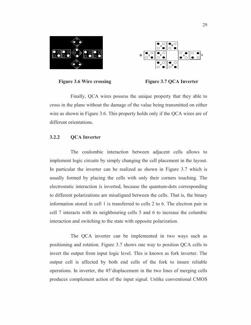
Figure 3.6 Wire crossing Figure 3.7 QCA Inverter
Finally, QCA wires possess the unique property that they able to
cross in the plane without the damage of the value being transmitted on either
wire as shown in Figure 3.6. This property holds only if the QCA wires are of
different orientations.
3.2.2 QCA Inverter
The coulombic interaction between adjacent cells allows to
implement logic circuits by simply changing the cell placement in the layout.
In particular the inverter can be realized as shown in Figure 3.7 which is
usually formed by placing the cells with only their corners touching. The
electrostatic interaction is inverted, because the quantum-dots corresponding
to different polarizations are misaligned between the cells. That is, the binary
information stored in cell 1 is transferred to cells 2 to 6. The electron pair in
cell 7 interacts with its neighbouring cells 5 and 6 to increase the columbic
interaction and switching to the state with opposite polarization.
The QCA inverter can be implemented in two ways such as
positioning and rotation. Figure 3.7 shows one way to position QCA cells to
invert the output from input logic level. This is known as fork inverter. The
output cell is affected by both end cells of the fork to insure reliable
operations. In inverter, the 45˚displacement in the two lines of merging cells
produces complement action of the input signal. Unlike conventional CMOS

� 30
in which it is the simplest block, the inverter consumes a substantial area in
QCA.
3.2.3 QCA Majority Gate
The fundamental QCA logic device is a three input majority gate. It
consists of five cells: a central logic cell, three input cells labelled A, B and C
and an output cell. The QCA majority gate performs a three-input logic
function. The logic function of the majority gate is
M (A, B, C) = AB+BC+CA. (3.3)
Figure 3.8 QCA majority gate layout and symbol
A layout of a QCA majority gate is shown in Figure 3.8. The
tendency of the majority device cell (central cell) to move to a ground state
ensures that it takes on the polarization of the majority of its neighbours. The
device cell will tend to follow the majority polarization because it represents
the lowest energy state. By fixing the polarization of one input to the QCA
majority gate as logic “1” or logic “0,” an AND gate or OR gate will be
obtained, respectively, as follows:
M(A,B,0) = AB (3.4)
M(A,B,1) = A+B (3.5)
Thus, we can base all QCA logic circuits on three-input majority gates. In
order to achieve efficient QCA design, majority gate-based design techniques
�

� 31
are required. The truth table of majority gate is shown below. The majority
gate output M (A, B, C) reflects the majority of inputs.
Table 3.1 Truth table of Majority gate
A B C M (A,B,C)
0 0 0 0
0 0 1 0
0 1 0 0
0 1 1 1
1 0 0 0
1 0 1 1
1 1 0 1
1 1 1 1
3.2.4 Nand-Nor-Inverter (NNI)
Pijush Kanti Bhattacharjee (2010) has done research on NNI gate.
The NNI gate is a universal gate. It can be employed for realizing logical
functions and requires less overhead, for setting the variables while realizing
the basic logic gates. NNI gate ensures very less space comparing to that of
the other gates like MV, AOI and inverter (NOT) gate.
The conventional AND and OR gates can be realized with the
majority gate by fixing an input as ‘0’ and ‘1’ respectively. The MG cannot
realize the logical NOT operation. The functionality complete set is {MG,
NOT}. Therefore, the designers have to use separate QCA cell arrangement
for realization of the logical NOT. Thus to implement MG with NOT function
the resulting gate is called Nand-Nor-Inverter gate as shown in Figure 3.11.

� 32
Figure 3.9 QCA NNI gate and Symbol
The truth table of NNI gate is shown below. The output of NNI
gate depends on the input B expect that all the inputs are equal. If all the
inputs are equal then the output is complement of inputs. The gate computes
the logic function as,
NNI (A, B, C) = M (A', B, C') = A'B+BC'+C'A'. (3.6)
Table 3.2 Truth table of NNI gate
A B C NNI(A,B,C)
0 0 0 1
0 0 1 0
0 1 0 1
0 1 1 1
1 0 0 0
1 0 1 0
1 1 0 1
1 1 1 0
3.2.5 AND-OR-Inverter (AOI)
Mariam Momenzadeh et al (2005) have proposed a complex QCA
gate. It is a 7 cell gate with 5 input cells, one device cell and one output cell.
The gate can be built from the original 5-cell MV by adding two extra inputs
(cells A and C); these two inputs have an inverting effect on the centre cell as

� 33
it can be seen from the layout of the inverter in Figure 3.7 that cells in a
diagonal orientation tend to exhibit an inverting function. It is an universal
QCA gate with embedded AND, OR and INV functions, and with better
usability for synthesis. The logic function realized by the AOI gate is:
F = DE + (D + E) (A' C' + A'B + BC'), (3.7)
= Maj (D, E, Maj (A', B, C')).
where Maj is the 3-input majority function.
Figure 3.10 AOI gate lay out and Symbol
Figure 3.11 AOI gate in terms of MV
The AOI gate is logically equivalent to a concatenation of two
majority voters (MV) with 2 complemented inputs (A and C) as shown in
Figure 3.11. The layout of AOI gate consists of two nested MVs. MV1
performs the function MV1= (A', B, C'). The horizontal input B has the
strongest influence on the center cell in a MV. Hence, in the AOI gate, the
cell B is placed further away than A and C. The second majority voter is MV2
= Maj (D, E, MV1).
In the AOI gate, the distances d1, d2 and d3 as shown in Figure
3.10 to be considered for proper operation of input and output binary wires.

� 34
The stable configuration of AOI the distances are fixed with d1= d3=
d4=25nm and d2=35nm.
3.2.6 Fanout
In a fanout, one signal comes in and several copies of input go out.
Each output reflects the input. The FANOUT is just the opposite of a majority
gate. In standard electronic, circuits a FANOUT is just a connection of several
metal wires.
Figure 3.12 QCA Fanout
3.2.7 Crossover Design
Walus et al (2004) have given two crossover options. There are
coplanar crossings and multilayer crossovers.
Crossing of two wires in one plane is achieved by placing a binary
wire (90˚) and inverter chain (45˚) as shown in Figure 3.6. The two signals are
able to cross each other without interference since the wires of different
orientation do not have any switch effect on each other .This is known as
coplanar crossings.
The Coplanar crossings use only one layer, but require two cell
types (regular and rotated). The regular cell and the rotated cell do not interact
with each other when they are properly aligned, so rotated cells can be used
for coplanar wire crossings. This feature allows the coplanar crossover to
transmit information independently along the two different cell wires. One

� 35
wire comprised of regular cells and other comprised of rotated cells as shown
in Figure 3.13. In the coplanar crossing, rotated cells are used when two wires
cross. By choosing the connection point from rotated cells, either an original
or an inverse of the input is available. If the effect of the vertical wire
consisting of the rotated cells could be ignored, then the information in
horizontal wire progress across the gap.
Figure 3.13 Coplanar crossover Figure 3.14 Multi layer crossover
Multilayer crossovers are used for wire crossings. They use
more than one layer of cells like bridge. The signals are transferred from one
layer to another layer using these multilayer QCA cells. To do this, it requires
a vertical interconnect. By stacking cells one on top of another, the signal can
be transmitted to another layer where the signal is again transmitted
horizontally.
The vertical separation between cells can be tuned to match the
Ekink of the horizontal cells. Unlike present CMOS integrated circuits, where
metal layers are used to connect discontinuous sections of a circuit and cannot
perform any intelligent functions, the extra layers of QCA can be used as
active components of the circuit. Hence the multilayer circuits can potentially
consume much less area as compared to coplanar circuits. On the other hand,
a multilayer crossover is quite straightforward from the design perspective
and the signal connection is steadier. The multilayer crossovers use more than
one layer of cells like multiple metal layers in a conventional IC.

� 36
3.2.8 QCA Clocking
In VLSI systems, timing is controlled through a reference signal
(i.e., a clock) and is mostly required for sequential circuits. Timing in QCA is
accomplished by clocking in four distinct and periodic phases and is needed
for both combinational and sequential circuits. Clocking provides control of
information flow and true power gain in QCA. Signal energy lost to the
environment is restored by the clock.
For QCA, the clock signals are generated through an electric
field, which is applied to the cells to either raise or lower the tunneling barrier
between dots within a QCA cell. When the barrier is low, the cells are in a
non-polarized state; when the barrier is high, the cells are not allowed to
change state. Adiabatic switching is achieved by lowering the barrier,
removing the previous input, applying the current input and then raising the
barrier. If transitions are gradual, the QCA system will remain close to the
ground state.
Clocking of QCA circuits has been explained by Heumpil Cho et al
(2007). It requires a completely different approach than CMOS. The cells are
not powered from any other external source apart from the clock. In order to
pump information down a circuit in a controllable manner four clocking zones
are available as shown in Figure 3.15. Each of clocking signal is phase shifted
by 90degrees with respect to one before.
Figure 3.15 QCA clocking zones Figure 3.16 The four phases of clock

� 37
The QCA clocks control the potential barrier between the dots. The
change in potential barrier allows to control the rate at which the electrons
quantum mechanically tunnel between the dots in the QCA cell and therefore,
the switching of its polarization.
When the clock signal is high the potential barriers between the
dots are low and electrons effectively spread out in the cell and no net
polarization exists (P = 0).As the clock signal is switched low, the potential
barriers between the dots are raised high and the electrons are localized such
that a polarization is developed based on the interaction of their neighbours.
When clock is high cell is unlatched and when clock is low cell is latched.
Cells can be grouped into zones so that the field influencing all the
cells in the zones will be the same. A zone cycles through 4 phases. Kyosun
Kim et al (2007) have explained about the 4 phases. In the Switch phase, the
tunneling barriers in a zone are raised. While this occurs, the electrons within
the cell can be influenced by the Columbic charges of neighbouring zones.
Zones in the Hold phase have a high tunneling barrier and will not change
state, but influence other adjacent zones. The Release and Relax phases
decrease the tunneling barrier so that the zone will not influence other zones.
The clock signals act to pump information in the circuit as a result
of the successive latching and unlatching in cells connected to different clock
phases. For example, a wire, which is clocked from left to right with
increasing clocking zones, will carry information in the same direction; i.e.,
from left to right.
Walus et al (2003) stated that the different part of the wire is
connected to the different clock signals. Figure 3.17 shows a wire connected
to different clock zones. Each group of cells connected to a particular
clocking zone can be described schematically as a D-latch. The decreasing

� 38
shades of gray represent increasing clocking zones. Since the cells in one
clock zone get latched and stay latched until the next groups of cells get
latched, they can be considered a D-latch. This is not a regular D-latch
because a group of cells connected to C1 will only transmit information to
cells connected to C2, never C0 nor C3. Figure 3.18 shows the D-latches with
the appropriate clock zone to obtain a schematic representation of the QCA
wire.
Figure 3.17 Clocked QCA wire
A low value of the clock means that the cells are latched. When the
clock signal is high, the cells are relaxed, and have no polarization. In
between, the cells are either latching or relaxing when the clock is decreasing
/increasing respectively. The minimum size of the clocking zone is
determined by the minimum feature size of the technology used to support
clocking. Large clocking zones can be problematic because signals travelling
down long QCA wires have increased probability of error from outside
influences. These include thermal effects, which can potentially flip the state
of a cell. Small clocking zones allow the designer the ability to create more
complicated and dense circuits.
3.3 QCADESIGNER
QCA logic and circuit designers require a rapid and accurate
simulation and design layout tool to determine the functionality of QCA
circuits. QCADesigner gives the designer the ability to quickly layout a QCA

� 39
design by providing an extensive set of Computer Aided Design (CAD) tools.
As well, several simulation engines facilitate rapid and accurate simulation. It
is the first publicly available design and simulation tool for QCA, developed
at the ATIPS Laboratory, at the University of Calgary. QCADesigner is
capable of simulating complex QCA circuits on most standard platforms. One
of the most important design specifications is that other developers should be
able to easily integrate their own utilities into QCADesigner. This is
accomplished by providing a standardized method of representing information
within the software. As well, simulation engines can easily be integrated into
QCADesigner using a standardized calling scheme and data types.
The QCADesigner has three distinct simulation engines. Each of
the three engines has a different and important set of benefits and drawbacks.
Additionally, each simulation engine can perform an exhaustive verification
of the system or a set of user-selected vectors.
3.3.1 Digital Simulation Engine
The digital simulation engine is a binary logic simulator within
QCADesigner. This engine considers each cell to be in one of three states:
null, logical one, or logical zero. With these three states and the appropriate
clocking zone information for each cell, a design can be quickly simulated to
ensure that for a given set of inputs, the correct set of outputs will be
produced. This allows the logic designer to determine if the structure that has
been laid out in QCADesigner corresponds to the desired logic function.
The simulator functions by first assigning values to the inputs of
the design. Then, for each change in the clock, only cells about to switch are
considered. Cells in the release and relax states are given a null value. Any
cells about to switch are processed by assigning them values based on the
QCA interaction rules and the polarization of cells in their neighbourhood.

� 40
After all switching cells have been processed, their values are examined to
ensure that none are null which ensures that the system will operate on all
cells. Upon completing this check, the clock cycle is finished and the next
cycle begins. This simulation will continue until all input combinations are
exhausted and the last input vector has traversed the system. Since each cell
can only receive input/output from its immediate neighbours in this engine,
most QCA structures are able to be handled.
The advantage of this simulator is that a designer can quickly see if
the logic functionality of a system corresponds to what is desired. Since no
physical information outside of cell locations and orientation is needed by the
simulator, it should remain an integral part of QCADesigner throughout its
lifetime.
3.3.2 Nonlinear Approximation Simulation Engine
The nonlinear approximation simulation engine is built on a
nonlinear approximation to the cell-to-cell response function. It has been
shown that two cells have a nonlinear cell-to-cell response function shown in
Figure 3.3. This approximation excludes the quantum mechanical correlations
between cells. The system is assumed to switch adiabatically, always
remaining very close to the ground state. The polarization state of each of the
cells is computed using
k
i , j
j
j
ik
i , j
j
j
EP
2P
E1 P
2
γ=
+ γ
∑
∑
(3.8)
where Pi is the polarization state of the cell, and Pj is the polarization state of
the neighbouring cells. Eki, j is the kink energy between cells, i and j represents
the energy cost of oppositely polarized cells, γ is the tunnelling potential and

� 41
is used to clock the circuit, as described by Walus (2004). Since
experimentally determined switching times are not available, the simulation
does not include any timing information. Using this response function the
simulation engine calculates the state of each cell with respect to other cells
within a predetermined effective radius. This calculation is iterated until the
entire system converges within a predetermined tolerance. Once the circuit
has converged, the output is recorded and new input values are set.
It is believed that although this approximation is sufficient to verify
the logical functionality of a design, it cannot be extended to include valid
dynamic simulation; but, as a result of its simplicity this simulation engine is
able to simulate a large number of cells very rapidly and, therefore, provides a
good, in process, check of a design. For a more accurate simulation the two-
state simulation engine is required.
3.3.3 Two-State Simulation Engine (Bistable simulation Engine)
To facilitate more accurate simulations we require a more advanced
simulation engine. The two-state model assumes that the cell is a simple two-
state system and it was proposed by Walus (2004). For this two-state system,
it has been shown that the following Hamiltonian (Hi) can be constructed.
k
j i , j i
i
kj
i j i, j
1P E
2H
1P E
2
− −γ =
−γ
∑ (3.9)
where Eki, j is the kink energy between cell i and j . This kink energy is
associated with the energy cost of two cells having opposite polarization. Pj is
the polarization of cell. γ is the tunneling energy of electrons within the cell.
The summation is over all cells within an effective radius of cell i, and can be
set prior to the simulation. Using the time-independent Schrödinger equation

� 42
we are able to find the stationary states of the cell in the environment
described by this Hamiltonian. QCADesigner uses the Jacobi algorithm to
find the eigenvalues and eigenvectors of the Hamiltonian with
Hi Ψi = Ei Ψi (3.10)
where Hi is the Hamiltonian given in Equation (3.9). Ψi is the state vector of
the cell. Ei is the energy associated with the state. The algorithm sorts each of
the states, Ψi, according to their respective energy, in ascending order. The
first state in the sorted list is that which has the lowest energy. Our
assumption is that the system remains very close to the ground state during
computation. As a result, the state with the lowest energy is chosen and the
cell polarization is set accordingly.
� The two state simulation engine computes the polarization of each
cell in the design until the entire system has converged to a preset tolerance.
Once the system has converged, the output values are recorded, new input
values are set and the simulation is reiterated.
This method is less efficient in comparison to the nonlinear
approximation, and as a result leads to longer simulation times. The
advantage of this method is that the model on which it is based is far more
accurate.
Before the simulation starts, the simulation parameters need to be
defined. All the simulations presented in this thesis use the bistable simulation
engine. All parameters use the default values provided by QCADesigner. The
following parameters are used for a bistable approximation:

� 43
Table 3.3 Truth table of simulation parameters
Parameters Values
Cell Size 20 nm
Number Of Samples 12800
Convergence Tolerance 0.001000
Radius of Effect 65nm
Relative Permittivity 12.9
Clock High 9.8e-22J
Clock Low 3.8e-23J
Clock Amplitude Factor 2
Layer Separation 11.5nm
Maximum Iteration Per Sample 10000
The definition of simulation parameters are given below:
Convergence Tolerance
During each sample, each cell is converged by the simulation
engine. The sample will complete when the polarization of each cell has
changed by less than this number; i.e. loop while any design cell has (old
polarization - new polarization) > convergence tolerance.
Radius of Effect
Because the interaction effect of one cell onto another decays
inversely with the fifth power of the distance between cells, need not to
consider each cell as affecting every other cell. This number determines how
far each cell will look to find its neighbours. The next-to-nearest neighbours
are included in this radius.

� 44
Figure 3.18 Radius effect of the cell. Figure 3.19 Clock signal
Note that with multilayer capability the radius of effect is extended
into the third dimension. Therefore in order to include cells in adjacent layers,
make sure that the layer separation is less than the radius of effect.
Relative Permittivity
The relative permittivity of the material is essential for simulation.
For GaAs/AlGaAs it is roughly 12.9 which is the default value. This is only
used in calculating the kink energy.
Clock Signal
The clock signal in QCADesigner is calculated as a hard-saturating
cosine as shown below. The clock signal is tied directly to the tunneling
energy in the Hamiltonian.
Clock High/Clock Low
Clock low and high values are the saturation energies for the clock
signal. When the clock is high the cell is unlatched. When it is low the cell is
latched.

� 45
Clock Shift
The clock shift is used to add a positive or negative offset to the
clock as shown in the Figure 3.19.
Clock Amplitude Factor
Clock amplitude factor is multiplied by (Clock High - Clock Low)
and reflects the amplitude of the underlying cosine.
Layer Separation
When simulating multilayer QCA circuits, this determines the
physical separation between the different cell layers in (nm).
Maximum Iterations per Sample
If the design does not converge in this number of iterations, then
the simulation will move on to the next sample point.
3.4 QCADESIGNER WINDOW
QCADesigner is the QCA layout editor and simulator. The main
layout design window of QCADesigner is presented in Figure 3.20.
Figure 3.20 QCADesigner layout editor window
� 46
The physical layout editing facilities include:
• Drawing QCA cells individually or in arrays, optionally aligned
to a grid with a default spacing (20 nm) equal to the default cell
size (18 nm) plus the default inter cell spacing (2 nm).
• Setting clock signal for each QCA cell, this is required to have
synchronous circuits working properly.
• Multi-layer QCA layout design, which is required to have multi
layer signal crossing.
• Drawing QCA cells with 90 degrees rotation, which is required
to have in plane signal crossing.
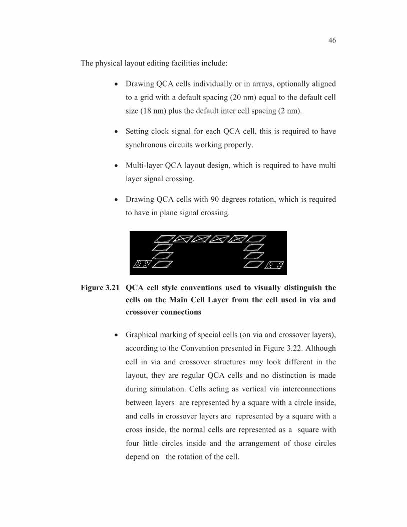
Figure 3.21 QCA cell style conventions used to visually distinguish the
cells on the Main Cell Layer from the cell used in via and
crossover connections
• Graphical marking of special cells (on via and crossover layers),
according to the Convention presented in Figure 3.22. Although
cell in via and crossover structures may look different in the
layout, they are regular QCA cells and no distinction is made
during simulation. Cells acting as vertical via interconnections
between layers are represented by a square with a circle inside,
and cells in crossover layers are represented by a square with a
cross inside, the normal cells are represented as a square with
four little circles inside and the arrangement of those circles
depend on the rotation of the cell.
� 47
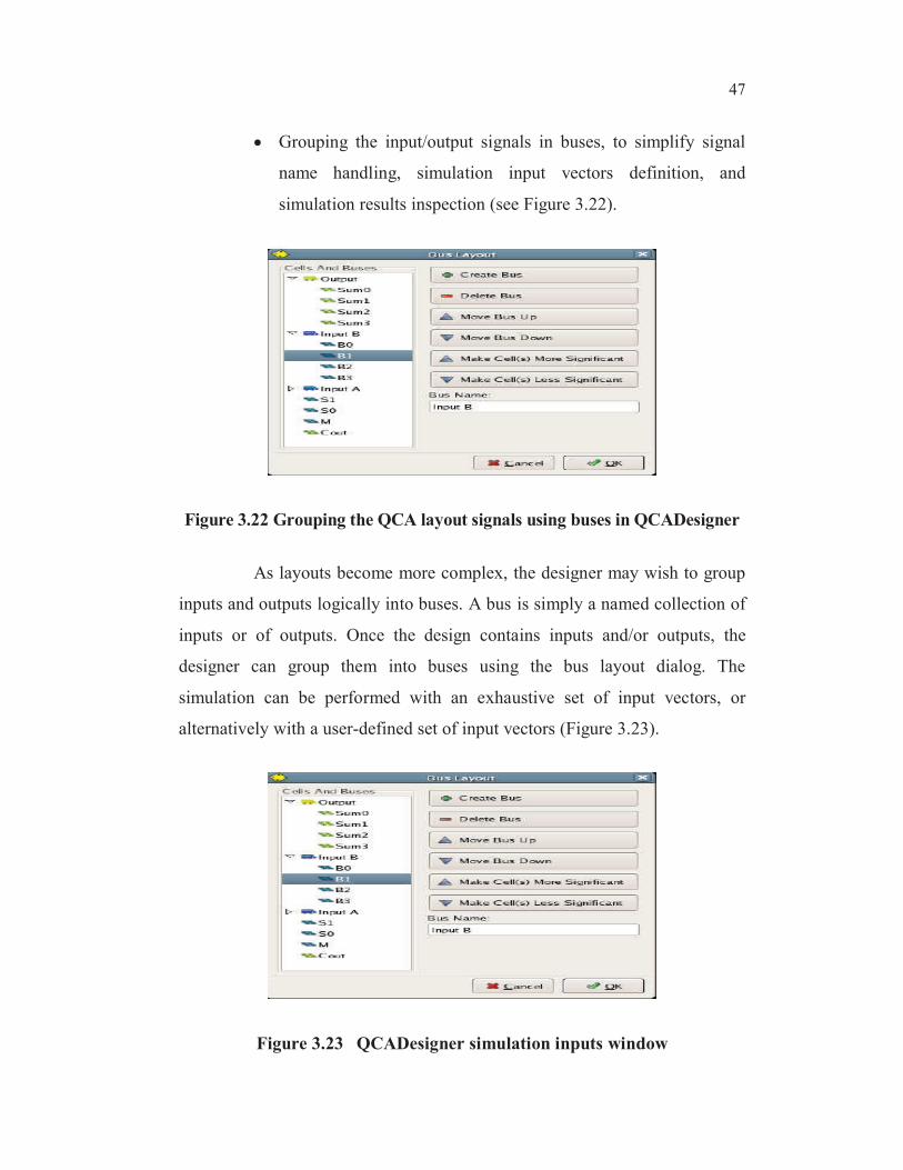
• Grouping the input/output signals in buses, to simplify signal
name handling, simulation input vectors definition, and
simulation results inspection (see Figure 3.22).
Figure 3.22 Grouping the QCA layout signals using buses in QCADesigner
As layouts become more complex, the designer may wish to group
inputs and outputs logically into buses. A bus is simply a named collection of
inputs or of outputs. Once the design contains inputs and/or outputs, the
designer can group them into buses using the bus layout dialog. The
simulation can be performed with an exhaustive set of input vectors, or
alternatively with a user-defined set of input vectors (Figure 3.23).
�
Figure 3.23 QCADesigner simulation inputs window

� 48
Figure 3.24 QCADesigner simulation results window
There are two integrated simulation engines available with
QCADesigner: the Coherence Vector Simulation Engine, which is slower, but
provides more accurate results, than the Bistable Simulation Engine.
Simulation results are presented as waveforms, optionally grouped in buses as
shown in Figure 3.24.
3.5 CONCLUSION
The relevant QCA background for this research is presented in this
Chapter 3, where the theoretical basis of Quantum Cellular Automata is
discussed. The basic logic elements of this technology and its operation are
explained here. A detailed explanation of the software tool QCADesigner is
presented in this Chapter. The different types of simulation engines and the
corresponding simulation parameters are defined here.
Related Documents