Chapter 2 Modern CMOS technology 1. Introduction. 2. CMOS process flow (continued). 1 rofabrication and thin film technology Bo Cui, ECE, University of Waterloo; http://ece.uwaterloo.ca/~bcui/ ilicon VLSI Technology by Plummer, Deal and Griffin

Chapter 2 Modern CMOS technology 1.Introduction. 2.CMOS process flow (continued). 1 NE 343: Microfabrication and thin film technology Instructor: Bo Cui,
Dec 16, 2015
Welcome message from author
This document is posted to help you gain knowledge. Please leave a comment to let me know what you think about it! Share it to your friends and learn new things together.
Transcript

1
Chapter 2 Modern CMOS technology
1. Introduction.
2. CMOS process flow (continued).
NE 343: Microfabrication and thin film technologyInstructor: Bo Cui, ECE, University of Waterloo; http://ece.uwaterloo.ca/~bcui/Textbook: Silicon VLSI Technology by Plummer, Deal and Griffin

2
Gate oxide growth
Remove resist, etch oxide, re-grow thermal oxide
The thin oxide over the active regions is stripped and a new gate oxide grown, typically 3 - 5nm, which could be grown in 0.5 - 1 hrs @ 800˚C in O2.
The ‘old’ oxide (to compensate stress of Si3N4) is too thick, and may be damaged during the several implantation steps.
Figure 2-24
3
Poly-crystalline silicon deposition
Poly-silicon is deposited by LPCVD ( ≈ 0.5 µm).
An unmasked P+ or As+ implant dopes the poly (typically 5 x 1015 cm-2, high doping to reduce gate resistance).
Both P and As have high solubility in Si, good for heavy doping.
When heated, they will diffuse quickly through grain boundary (now that poly) to achieve uniform doping.
MOSFET: metal oxide semiconductor field effect transistorBut actually metal is no longer used, instead, low resistance heavily doped poly-Si is used.
LPCVD poly-Si: SiH4 Si + 2H2.
4
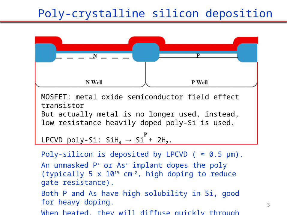
Gate formation
Mask #6 is used to protect the MOS gates.
The poly-Si is plasma etched using an anisotropic etch.
Spin resist, photolithography, selective anisotropic etch of poly-Si.
The photolithography in this step is the most demanding since it requires the finestresolution to create the narrow MOS channels.
Poly: poly-crystalline(not single crystal)
Poly-Si can also be used for local wiring. But not for long wiring as it is resistance is still much higher than metal.
5
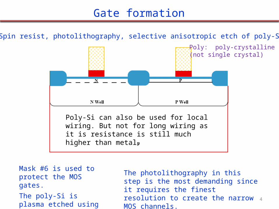
Tip or extension/LDD (lightly doped drain) formation
Mask #7 protects the PMOS devices.
A P+ implant forms the LDD regions in the NMOS devices.
Typically 5 x 1013cm-2 @ 50 KeV.
Strip resist, spin resist, photolithography, ion implantation
The polysilicon gate acts like a barrier for this implant to protect the channel region.This is thus a self-aligned process.
When channel length shrinks more than drive voltage, electric field in the channel may become very high, creating “hot electrons” that may create additional hole-electron pair or inject into gate oxide.
LDD (graded doping) allows drain voltage to be dropped over larger distance, thus reducing peak electric field/hot electron effect.Figure 2-27

6
Tip or extension/LDD (lightly doped drain) formation
Remove resist, spin resist, photolithography, B+ ion implantation
Mask #8 protects the NMOS devices.
A B+ implant forms the LDD regions in the PMOS devices.
Typically 5 x 1013cm-2 @ 50 KeV.
As LDD is shallower than N+ and P+ source/drain doping, it also reduces “short channel effect” due to the shallower channel.
7
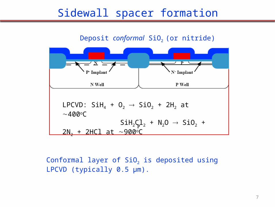
Sidewall spacer formation
Deposit conformal SiO2 (or nitride)
Conformal layer of SiO2 is deposited using LPCVD (typically 0.5 µm).
LPCVD: SiH4 + O2 SiO2 + 2H2 at 400oC SiH2Cl2 + N2O SiO2 + 2N2 + 2HCl at 900oC
8
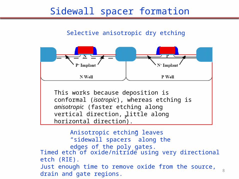
Sidewall spacer formation
Anisotropic etching leaves “sidewall spacers” along the edges of the poly gates.
Selective anisotropic dry etching
Timed etch of oxide/nitride using very directional etch (RIE).Just enough time to remove oxide from the source, drain and gate regions.
This works because deposition is conformal (isotropic), whereas etching is anisotropic (faster etching along vertical direction, little along horizontal direction).
9
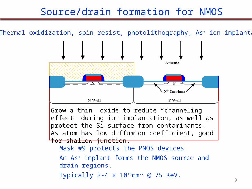
Source/drain formation for NMOS
Mask #9 protects the PMOS devices.
An As+ implant forms the NMOS source and drain regions.
Typically 2-4 x 1015cm-2 @ 75 KeV.
Thermal oxidization, spin resist, photolithography, As+ ion implantation
Grow a thin oxide to reduce “channeling effect” during ion implantation, as well as protect the Si surface from contaminants.As atom has low diffusion coefficient, good for shallow junction.

10
Source/drain formation for PMOS
Strip resist, spin resist, photolithography, B+ ion implantation
Mask #10 protects the NMOS devices.
A B+ implant forms the PMOS source and drain regions.
Typically 1-3 x 1015cm-2 @ 50 KeV.
Again, high dose implant to reduce parasitic resistance in the source/drain region.
Figure 2-32
11
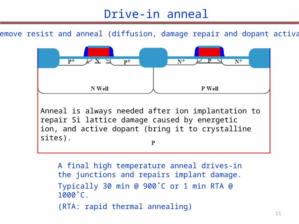
Drive-in anneal
Remove resist and anneal (diffusion, damage repair and dopant activation)
A final high temperature anneal drives-in the junctions and repairs implant damage.
Typically 30 min @ 900˚C or 1 min RTA @ 1000˚C.
(RTA: rapid thermal annealing)
Anneal is always needed after ion implantation to repair Si lattice damage caused by energetic ion, and active dopant (bring it to crystalline sites).
12
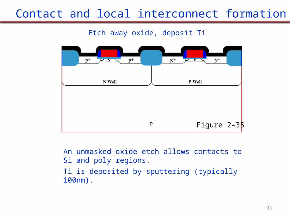
Contact and local interconnect formation
Etch away oxide, deposit Ti
An unmasked oxide etch allows contacts to Si and poly regions.
Ti is deposited by sputtering (typically 100nm).
Figure 2-35
13
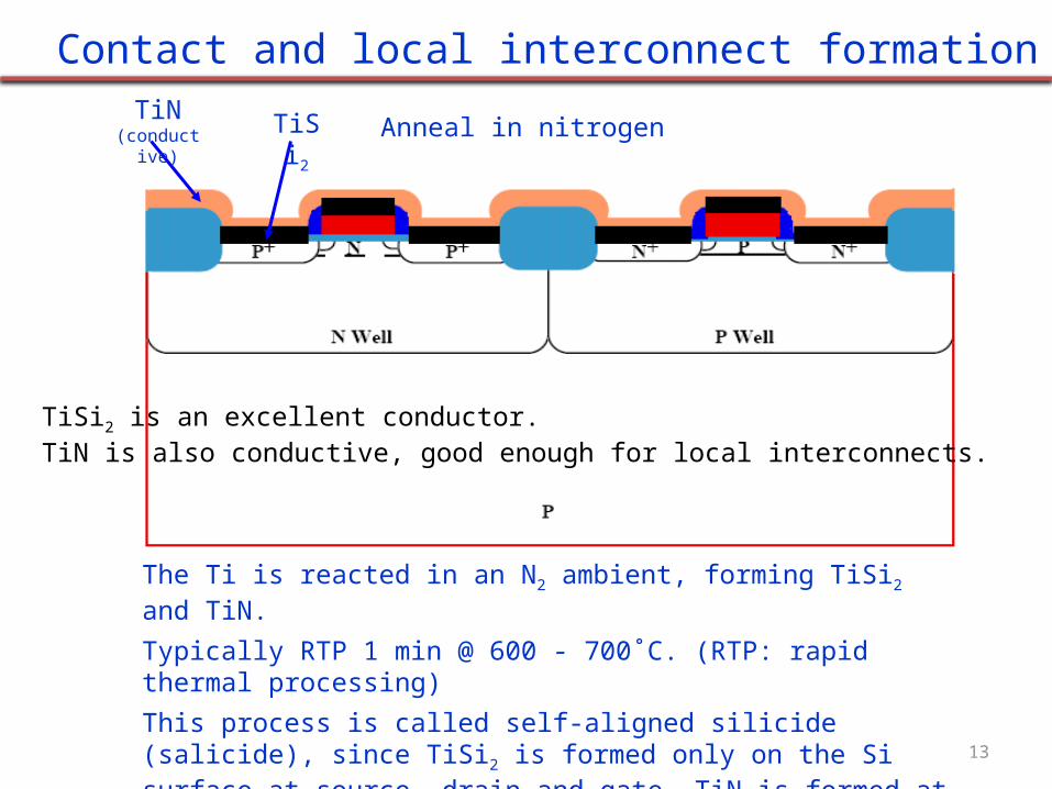
TiN(conductive
)
TiSi2 Anneal in nitrogen
Contact and local interconnect formation
The Ti is reacted in an N2 ambient, forming TiSi2 and TiN.
Typically RTP 1 min @ 600 - 700˚C. (RTP: rapid thermal processing)
This process is called self-aligned silicide (salicide), since TiSi2 is formed only on the Si surface at source, drain and gate. TiN is formed at SiO2 surface.
Salicide reduces gate resistance, source/drain contact resistance.
TiSi2 is an excellent conductor.TiN is also conductive, good enough for local interconnects.
14
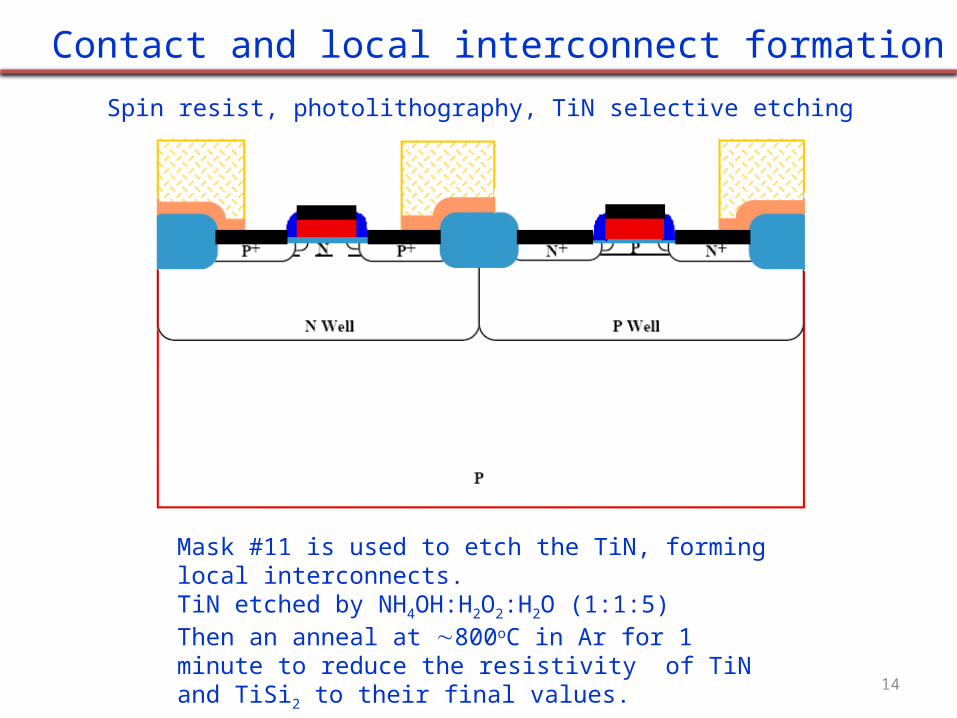
Contact and local interconnect formation
Spin resist, photolithography, TiN selective etching
Mask #11 is used to etch the TiN, forming local interconnects.TiN etched by NH4OH:H2O2:H2O (1:1:5)Then an anneal at 800oC in Ar for 1 minute to reduce the resistivity of TiN and TiSi2 to their final values.

15
Multi-level metal formation
Remove resist, deposit SiO2
A conformal layer of SiO2 is deposited by LPCVD (typically 1 µm).
The SiO2 layer is often doped with P (PSG – phosphosilicate glass) that protects the device against mobile ions like Na+.B may also be added (BPSG – borophosphosilicate glass) to reduce the flowing temperature of the glass (flow to smooth out the surface, good for planarization).

16
Surface planarization
Chemical mechanical polishing (CMP)
Besides CMP, planarization can also be done by spinning resist and etching back, using a recipe where etching rates for resist and glass are the same.
In CMP, besides mechanical polishing (by nanoparticles in the slurry), chemical reaction (e.g. by adjusting pH) is also important.The total polishing rate is much higher than mechanical polishing rate and chemical reaction rate alone.
17
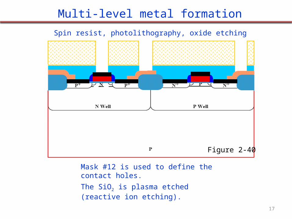
Multi-level metal formation
Spin resist, photolithography, oxide etching
Mask #12 is used to define the contact holes.
The SiO2 is plasma etched (reactive ion etching).
Figure 2-40
18
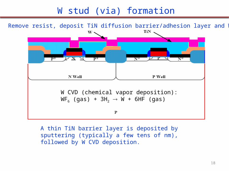
W stud (via) formation
Remove resist, deposit TiN diffusion barrier/adhesion layer and W
A thin TiN barrier layer is deposited by sputtering (typically a few tens of nm), followed by W CVD deposition.
W CVD (chemical vapor deposition):WF6 (gas) + 3H2 W + 6HF (gas)
19
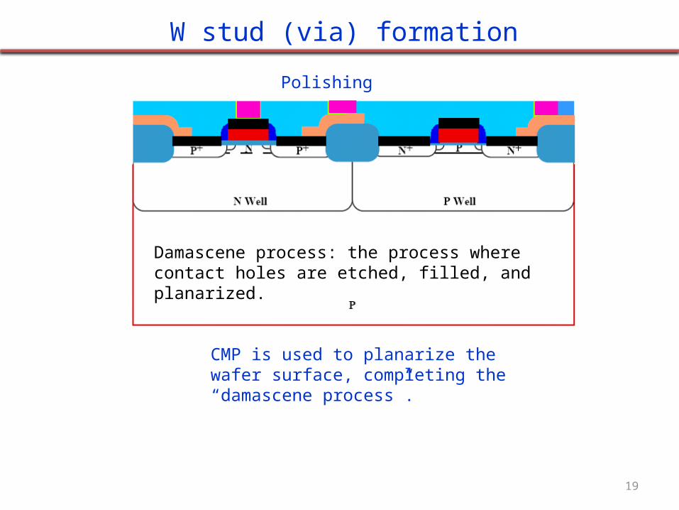
W stud (via) formation
Polishing
CMP is used to planarize the wafer surface, completing the “damascene process”.
Damascene process: the process where contact holes are etched, filled, and planarized.
20
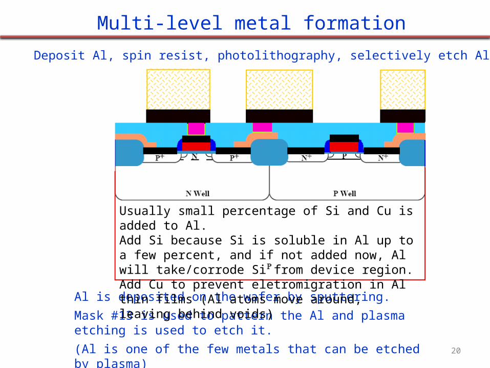
Deposit Al, spin resist, photolithography, selectively etch Al
Multi-level metal formation
Al is deposited on the wafer by sputtering.
Mask #13 is used to pattern the Al and plasma etching is used to etch it.
(Al is one of the few metals that can be etched by plasma)
Usually small percentage of Si and Cu is added to Al.Add Si because Si is soluble in Al up to a few percent, and if not added now, Al will take/corrode Si from device region.Add Cu to prevent eletromigration in Al thin films (Al atoms move around, leaving behind voids)

21
P
Multi-level metal formation
Strip resist, deposit insulator layer, W stud and Al wire formation,Si3N4 passivation layer deposition.
Inter-metal dielectric and second level metal are deposited and defined in the same way as level #1.Mask #14 is used to define contact via-holes.Mask #15 is used to define metal 2.Passivation/protection layer of Si3N4 is deposited by PECVD and patterned with Mask #16.
Final anneal (400-500oC, 30min, in forming gas – 10% H2 in N2) to alloy the metal contacts and reduce electrical charges in the Si/SiO2 interfaces.

22
Wire bonding and packaging
Finish the device
P
(source gate drain)
23
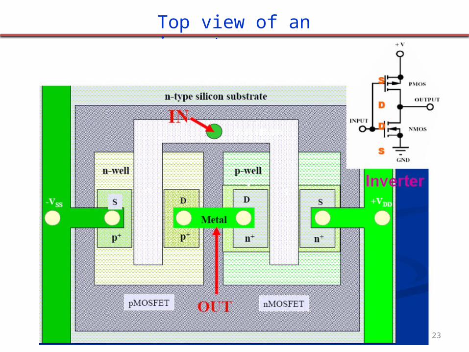
Top view of an inverter

24
90 nm generation
transistor and interconnect Carrier
moves faster in strained Si
Ni silicide (not Ti silicide).
Only 1.2nm gate oxide.
Strained silicon.
Low-k dielectric (lower , than SiO2,) to reduce capacitance and RC delay for faster circuit.
Copper interconnect (not Al) by electroplating and chemical mechanical polishing (see next slide).

25
Advanced metallization: Cu based
Dual damascene IC process
26
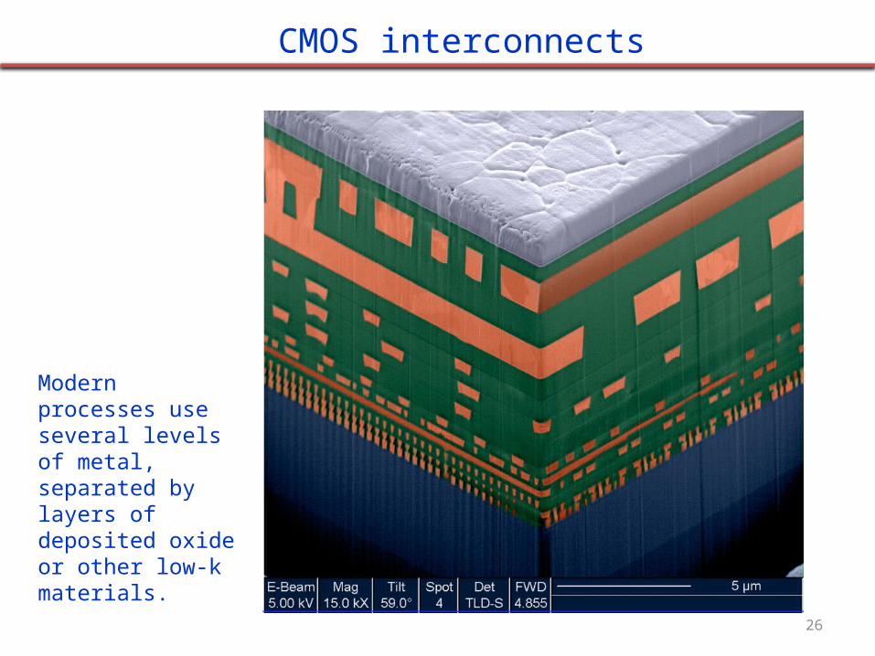
Modern processes use several levels of metal, separated by layers of deposited oxide or other low-k materials.
CMOS interconnects
Related Documents